WO2024127989A1 - 多層基板及び多層基板の製造方法 - Google Patents
多層基板及び多層基板の製造方法 Download PDFInfo
- Publication number
- WO2024127989A1 WO2024127989A1 PCT/JP2023/042681 JP2023042681W WO2024127989A1 WO 2024127989 A1 WO2024127989 A1 WO 2024127989A1 JP 2023042681 W JP2023042681 W JP 2023042681W WO 2024127989 A1 WO2024127989 A1 WO 2024127989A1
- Authority
- WO
- WIPO (PCT)
- Prior art keywords
- conductor
- columnar
- layer
- axis
- conductor layer
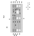
- Prior art date
- Legal status (The legal status is an assumption and is not a legal conclusion. Google has not performed a legal analysis and makes no representation as to the accuracy of the status listed.)
- Ceased
Links
Images









Classifications
-
- H—ELECTRICITY
- H05—ELECTRIC TECHNIQUES NOT OTHERWISE PROVIDED FOR
- H05K—PRINTED CIRCUITS; CASINGS OR CONSTRUCTIONAL DETAILS OF ELECTRIC APPARATUS; MANUFACTURE OF ASSEMBLAGES OF ELECTRICAL COMPONENTS
- H05K1/00—Printed circuits
- H05K1/02—Details
- H05K1/11—Printed elements for providing electric connections to or between printed circuits
- H05K1/115—Via connections; Lands around holes or via connections
-
- H—ELECTRICITY
- H01—ELECTRIC ELEMENTS
- H01P—WAVEGUIDES; RESONATORS, LINES, OR OTHER DEVICES OF THE WAVEGUIDE TYPE
- H01P3/00—Waveguides; Transmission lines of the waveguide type
- H01P3/02—Waveguides; Transmission lines of the waveguide type with two longitudinal conductors
- H01P3/08—Microstrips; Strip lines
-
- H—ELECTRICITY
- H05—ELECTRIC TECHNIQUES NOT OTHERWISE PROVIDED FOR
- H05K—PRINTED CIRCUITS; CASINGS OR CONSTRUCTIONAL DETAILS OF ELECTRIC APPARATUS; MANUFACTURE OF ASSEMBLAGES OF ELECTRICAL COMPONENTS
- H05K1/00—Printed circuits
- H05K1/02—Details
-
- H—ELECTRICITY
- H05—ELECTRIC TECHNIQUES NOT OTHERWISE PROVIDED FOR
- H05K—PRINTED CIRCUITS; CASINGS OR CONSTRUCTIONAL DETAILS OF ELECTRIC APPARATUS; MANUFACTURE OF ASSEMBLAGES OF ELECTRICAL COMPONENTS
- H05K1/00—Printed circuits
- H05K1/02—Details
- H05K1/0213—Electrical arrangements not otherwise provided for
- H05K1/0237—High frequency adaptations
-
- H—ELECTRICITY
- H05—ELECTRIC TECHNIQUES NOT OTHERWISE PROVIDED FOR
- H05K—PRINTED CIRCUITS; CASINGS OR CONSTRUCTIONAL DETAILS OF ELECTRIC APPARATUS; MANUFACTURE OF ASSEMBLAGES OF ELECTRICAL COMPONENTS
- H05K1/00—Printed circuits
- H05K1/02—Details
- H05K1/0213—Electrical arrangements not otherwise provided for
- H05K1/0237—High frequency adaptations
- H05K1/025—Impedance arrangements, e.g. impedance matching, reduction of parasitic impedance
- H05K1/0251—Impedance arrangements, e.g. impedance matching, reduction of parasitic impedance related to vias or transitions between vias and transmission lines
-
- H—ELECTRICITY
- H05—ELECTRIC TECHNIQUES NOT OTHERWISE PROVIDED FOR
- H05K—PRINTED CIRCUITS; CASINGS OR CONSTRUCTIONAL DETAILS OF ELECTRIC APPARATUS; MANUFACTURE OF ASSEMBLAGES OF ELECTRICAL COMPONENTS
- H05K3/00—Apparatus or processes for manufacturing printed circuits
- H05K3/46—Manufacturing multilayer circuits
-
- H—ELECTRICITY
- H05—ELECTRIC TECHNIQUES NOT OTHERWISE PROVIDED FOR
- H05K—PRINTED CIRCUITS; CASINGS OR CONSTRUCTIONAL DETAILS OF ELECTRIC APPARATUS; MANUFACTURE OF ASSEMBLAGES OF ELECTRICAL COMPONENTS
- H05K3/00—Apparatus or processes for manufacturing printed circuits
- H05K3/46—Manufacturing multilayer circuits
- H05K3/4644—Manufacturing multilayer circuits by building the multilayer layer by layer, i.e. build-up multilayer circuits
-
- H—ELECTRICITY
- H05—ELECTRIC TECHNIQUES NOT OTHERWISE PROVIDED FOR
- H05K—PRINTED CIRCUITS; CASINGS OR CONSTRUCTIONAL DETAILS OF ELECTRIC APPARATUS; MANUFACTURE OF ASSEMBLAGES OF ELECTRICAL COMPONENTS
- H05K2201/00—Indexing scheme relating to printed circuits covered by H05K1/00
- H05K2201/10—Details of components or other objects attached to or integrated in a printed circuit board
- H05K2201/10227—Other objects, e.g. metallic pieces
- H05K2201/10242—Metallic cylinders
Definitions
- the present invention relates to a multilayer substrate having a structure in which multiple insulating layers are stacked.
- a known example of a conventional invention related to a multilayer board is the method for manufacturing a wired circuit board described in Patent Document 1.
- a seed film and wiring are layered on top of a base insulating layer.
- the seed film and wiring are made of conductors. This reduces the resistance of the current path including the seed film and wiring.
- the object of the present invention is to provide a multilayer board and a method for manufacturing a multilayer board that can reduce the resistance of the current path.
- a multilayer substrate comprises:
- the semiconductor device includes at least a laminate, a first conductor layer, a second conductor layer, a first columnar conductor, a second columnar conductor, and a connecting conductor
- the laminate has a structure in which a plurality of insulator layers including a first insulator layer are laminated along a Z axis, the first insulator layer has a positive principal surface and a negative principal surface located on the negative side of the Z axis from the positive principal surface, the first conductor layer and the second conductor layer are located on the positive principal surface of the first insulator layer;
- the first columnar conductor and the second columnar conductor are provided inside through holes that penetrate the first insulating layer along the Z-axis, an end portion of the first columnar conductor on the positive side in the Z-axis direction is in contact with the first conductor layer;
- the connecting conductor is a conductor that electrically connects the conductors in the stacking direction, an end portion of the first columnar conduct
- a method for manufacturing a multilayer substrate includes the steps of: A method for manufacturing a multilayer substrate, comprising a first preparation step, a through hole forming step, a conductor layer forming step, a columnar conductor forming step, a second preparation step, and a pressure bonding step,
- a first preparation step a first insulator layer is prepared, the first insulator layer having a positive main surface and a negative main surface located on the negative side of the positive main surface along the Z axis, the first insulator layer being provided with a metal foil covering the positive main surface;
- the through hole forming step a first through hole and a second through hole penetrating along the Z axis are formed in the first insulator layer,
- a first conductor layer and a second conductor layer are formed by processing the metal foil;
- a first columnar conductor forming step a first columnar conductor and a second columnar conductor are formed in the first through hole and the second
- the multilayer board and the method for manufacturing the multilayer board according to the present invention can reduce the resistance of the current path.
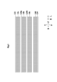
- FIG. 1 is an exploded perspective view of a multilayer substrate 10.
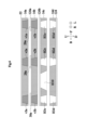
- FIG. FIG. 2 is a cross-sectional view of the multilayer substrate 10.
- FIG. 3 is a cross-sectional view of the multilayer substrate 10 during its manufacture.
- FIG. 4 is a cross-sectional view of the multilayer substrate 10 during its manufacture.
- FIG. 5 is a cross-sectional view of the multilayer substrate 10 during its manufacture.
- FIG. 6 is a cross-sectional view of the multilayer substrate 10 during its manufacture.
- FIG. 7 is a cross-sectional view of the multilayer substrate 10 during its manufacture.
- FIG. 8 is a cross-sectional view of the multilayer substrate 10 during its manufacture.
- FIG. 9 is a cross-sectional view of the multilayer substrate 10 during its manufacture.
- FIG. 1 is an exploded perspective view of a multilayer substrate 10.
- FIG. 2 is a cross-sectional view of the multilayer substrate 10.
- FIG. 3 is a cross-sectional view of the multilayer substrate 10
- FIG. 10 is a cross-sectional view of the multilayer substrate 10 during its manufacture.
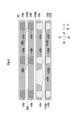
- FIG. 11 is a cross-sectional view of the multilayer substrate 10a.
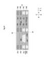
- FIG. 12 is a cross-sectional view of the multilayer substrate 10b.
- FIG. 13 is a top view of an insulator layer 16c of a multi-layer substrate 10c.
- FIG. 14 is a top view of an insulator layer 16c of a multi-layer substrate 10d.
- FIG. 15 is a rear view of the multilayer board 10d when in use.
- FIG. 16 is a top view of an insulator layer 16c of a multi-layer substrate 10e.
- FIG. 1 is an exploded perspective view of the multilayer substrate 10.
- Fig. 2 is a cross-sectional view of the multilayer substrate 10.
- Fig. 2 shows a cross-section taken along line A-A in Fig. 1. Note that in Fig. 1, reference symbols are given only to representative columnar conductors v1a-v1d, v2a-v2d, and v3a-v3d among the multiple columnar conductors v1a-v1d, v2a-v2d, and v3a-v3d.
- the stacking direction of the laminate 12 of the multilayer substrate 10 is defined as the up-down direction.
- the up-down direction coincides with the Z-axis direction.
- the up-down direction is the positive direction of the Z-axis.
- the down-down direction is the negative direction of the Z-axis.
- the extension direction of the signal conductor layer 20a and the power conductor layer 20b of the multilayer substrate 10 is defined as the left-right direction.
- the line width direction of the signal conductor layer 20a and the power conductor layer 20b when viewed in the up-down direction is defined as the front-rear direction.
- the up-down direction, front-rear direction, and left-right direction are mutually orthogonal.
- the up-down direction and the down direction may be interchanged, the left direction and the right direction may be interchanged, and the front direction and the rear direction may be interchanged.
- X is a part or member of the multilayer substrate 10.
- each part of X is defined as follows:
- the front part of X means the front half of X.
- the rear part of X means the rear half of X.
- the left part of X means the left half of X.
- the right part of X means the right half of X.
- the upper part of X means the upper half of X.
- the lower part of X means the lower half of X.
- the front end of X means the front end of X.
- the rear end of X means the rear end of X.
- the left end of X means the left end of X.
- the right end of X means the right end of X.
- the upper end of X means the upper end of X.
- the lower end of X means the lower end of X.
- the front end of X means the front end of X and its vicinity.
- the rear end of X means the rear end of X and its vicinity.
- the left end of X means the left end of X and its vicinity.
- the right end of X means the right end of X and its vicinity.
- the upper end of X means the upper end of X and its vicinity.
- the lower end of X means the lower end of X and its vicinity.
- the multilayer board 10 transmits high-frequency signals.
- the multilayer board 10 is used to electrically connect two circuits in electronic devices such as smartphones.
- the multilayer board 10 includes a laminate 12, protective layers 18a and 18b, a signal conductor layer 20a, a power conductor layer 20b, a first ground conductor layer 22, a second ground conductor layer 24, ground conductor layers 26a, 26b, 28a, 28b, 30a, and 30b, a plurality of columnar conductors v1a to v1d, a plurality of columnar conductors v2a to v2d, a plurality of columnar conductors v3a to v3d, a columnar conductor v10, and connecting conductors v11d, v12d, and v13d.
- the connecting conductors v11d, v12d, and v13d are made of different materials from the columnar conductor
- the laminate 12 has a plate shape. Therefore, the laminate 12 has an upper main surface (positive main surface) and a lower main surface (negative main surface) located below the upper main surface (positive main surface) (negative side of the Z axis).
- the upper and lower main surfaces of the laminate 12 have a rectangular shape with long sides extending along the left-right axis. Therefore, the left-right length of the laminate 12 is longer than the front-rear length of the laminate 12.
- the laminate 12 is flexible.
- the laminate 12 has a structure in which the insulator layers 16a to 16d, including the insulator layer 16c (first insulator layer), are stacked along the vertical axis (Z axis).
- the insulator layers 16a to 16d are arranged in this order from top to bottom.
- the insulator layers 16a to 16d have an upper main surface (positive main surface) and a lower main surface (negative main surface) located below the upper main surface (positive main surface) (on the negative side of the Z axis).
- the material of the insulator layers 16a to 16d is, for example, a thermoplastic resin.
- the thermoplastic resin is, for example, a liquid crystal polymer.
- the insulator layers 16a to 16d are fused together with adjacent ones vertically.
- a high-frequency signal is transmitted to the signal conductor layer 20a.
- the signal conductor layer 20a (third conductor layer) is located on the upper main surface (front main surface) of the insulator layer 16c (first insulator layer).
- the signal conductor layer 20a When viewed in the downward direction, the signal conductor layer 20a has a linear shape extending along the left-right axis.
- the signal conductor layer 20a has an upper main surface and a lower main surface located below the upper main surface. The surface roughness of the lower main surface of the signal conductor layer 20a is greater than the surface roughness of the upper main surface of the signal conductor layer 20a.
- a power supply potential is connected to the power supply conductor layer 20b.
- the power supply conductor layer 20b (second conductor layer) is located on the upper main surface (positive main surface) of the insulator layer 16c (first insulator layer).
- the power supply conductor layer 20b When viewed downward (negative direction of the Z axis), the power supply conductor layer 20b has a linear shape extending along the left-right axis. Therefore, the power supply conductor layer 20b is parallel to the signal conductor layer 20a.
- the power supply conductor layer 20b is located behind the signal conductor layer 20a.
- the line width Wb of the power supply conductor layer 20b is larger than the line width Wa of the signal conductor layer 20a.
- the power supply conductor layer 20b (second conductor layer) has an upper main surface (positive main surface) and a lower main surface (negative main surface) located below the upper main surface (positive main surface) (negative side of the Z axis).
- the surface roughness of the lower main surface (negative main surface) of the power conductor layer 20b is greater than the surface roughness of the upper main surface (positive main surface) of the power conductor layer 20b.
- the first ground conductor layer 22 is provided in the laminate 12 as shown in FIG. 1.
- the first ground conductor layer 22 is located above the signal conductor layer 20a and the power conductor layer 20b, and overlaps with the signal conductor layer 20a and the power conductor layer 20b when viewed downward.
- the first ground conductor layer 22 is located on the upper main surface of the insulator layer 16a.
- the first ground conductor layer 22 covers substantially the entire upper main surface of the insulator layer 16a.
- the first ground conductor layer 22 has an upper main surface and a lower main surface located below the upper main surface. The surface roughness of the lower main surface of the first ground conductor layer 22 is greater than the surface roughness of the upper main surface of the first ground conductor layer 22.
- a ground potential is connected to the first ground conductor layer 22.
- the second ground conductor layer 24 is provided in the laminate 12 as shown in FIG. 1.
- the second ground conductor layer 24 is located below the signal conductor layer 20a and the power conductor layer 20b, and overlaps the signal conductor layer 20a and the power conductor layer 20b when viewed in the downward direction.
- the second ground conductor layer 24 is located on the lower main surface of the insulator layer 16d.
- the second ground conductor layer 24 covers substantially the entire lower main surface of the insulator layer 16d.
- the second ground conductor layer 24 has an upper main surface and a lower main surface located below the upper main surface.
- the surface roughness of the upper main surface of the second ground conductor layer 24 is greater than the surface roughness of the lower main surface of the second ground conductor layer 24.
- a ground potential is connected to the second ground conductor layer 24.
- the signal conductor layer 20a, the first ground conductor layer 22, and the second ground conductor layer 24 as described above have a stripline structure.
- the ground conductor layers 26a, 28a, and 30a are provided in the laminate 12 as shown in FIG. 1.
- the ground conductor layers 26a, 28a, and 30a do not overlap the signal conductor layer 20a and the power conductor layer 20b when viewed downward.
- the ground conductor layers 26a, 28a, and 30a are located on the upper main surface of the insulator layer 16b.
- the ground conductor layers 26a, 28a, and 30a have a linear shape extending in the left-right direction.
- the ground conductor layer 26a is located in front of the signal conductor layer 20a.
- the ground conductor layer 28a is located behind the signal conductor layer 20a and in front of the power conductor layer 20b.
- the ground conductor layer 30a When viewed downward, the ground conductor layer 30a is located behind the power conductor layer 20b.
- the ground conductor layers 26a, 28a, and 30a have an upper main surface and a lower main surface located below the upper main surface.
- the surface roughness of the lower principal surfaces of the ground conductor layers 26a, 28a, and 30a is greater than the surface roughness of the upper principal surfaces of the ground conductor layers 26a, 28a, and 30a.
- the ground conductor layers 26b, 28b, and 30b are provided in the laminate 12 as shown in FIG. 1.
- the ground conductor layers 26b, 28b, and 30b do not overlap the signal conductor layer 20a and the power conductor layer 20b when viewed from below.
- the ground conductor layers 26b, 28b, and 30b (first conductor layers) are located on the upper main surface of the insulator layer 16c.
- the ground conductor layers 26b, 28b, and 30b have a linear shape extending in the left-right direction when viewed from below.
- the ground conductor layer 26b is located in front of the signal conductor layer 20a when viewed from below.
- the ground conductor layer 28b is located behind the signal conductor layer 20a and in front of the power conductor layer 20b when viewed from below.
- the ground conductor layer 30b is located behind the power conductor layer 20b when viewed from below.
- the ground conductor layers 26b, 28b, and 30b have an upper main surface and a lower main surface that is located below the upper main surface.
- the surface roughness of the lower principal surfaces of the ground conductor layers 26b, 28b, and 30b is greater than the surface roughness of the upper principal surfaces of the ground conductor layers 26b, 28b, and 30b.
- the columnar conductors v1a, v2a, and v3a penetrate the insulator layer 16a along the vertical axis.
- the columnar conductors v1a, v2a, and v3a have a section in which the thickness of the columnar conductors v1a, v2a, and v3a decreases toward the top.
- the upper ends of the columnar conductors v1a contact the first ground conductor layer 22.
- the lower ends of the columnar conductors v1a contact the ground conductor layer 26a.
- the columnar conductors v1a are aligned in a line along the horizontal axis.
- the upper ends of the columnar conductors v2a contact the first ground conductor layer 22.
- the lower ends of the columnar conductors v2a contact the ground conductor layer 28a.
- the columnar conductors v2a are aligned in a line along the horizontal axis.
- the upper ends of the columnar conductors v3a contact the first ground conductor layer 22.
- the lower ends of the multiple columnar conductors v3a are in contact with the ground conductor layer 30a.
- the multiple columnar conductors v3a are aligned in a row along the left-right axis.
- the columnar conductors v1b, v2b, and v3b penetrate the insulator layer 16b along the vertical axis.
- the columnar conductors v1b, v2b, and v3b have a section in which the thickness of the columnar conductors v1b, v2b, and v3b decreases toward the top.
- the upper ends of the columnar conductors v1b are in contact with the ground conductor layer 26a.
- the lower ends of the columnar conductors v1b are in contact with the ground conductor layer 26b.
- the columnar conductors v1b are aligned in a line along the horizontal axis.
- the upper ends of the columnar conductors v2b are in contact with the ground conductor layer 28a.
- the lower ends of the columnar conductors v2b are in contact with the ground conductor layer 28b.
- the columnar conductors v2b are aligned in a line along the horizontal axis.
- the upper ends of the columnar conductors v3b are in contact with the ground conductor layer 30a.
- the lower ends of the columnar conductors v3b are in contact with the ground conductor layer 30b.
- the multiple columnar conductors v3b are aligned in a row along the left-right axis.
- the multiple columnar conductors v1c, v2c, v3c are provided in through holes that penetrate the insulator layer 16c (first insulator layer) along the vertical axis.
- the multiple columnar conductors v1c, v2c, v3c penetrate the insulator layer 16c (first insulator layer) along the vertical axis.
- the multiple columnar conductors v1c, v2c, v3c (first columnar conductors) have a section in which the thickness of the multiple columnar conductors v1c, v2c, v3c decreases as they move upward (positive direction of the Z axis).
- the upper ends of the multiple columnar conductors v1c are in contact with the ground conductor layer 26b.
- the multiple columnar conductors v1c are aligned in a line along the horizontal axis.
- the upper ends (first columnar conductors) of the multiple columnar conductors v2c are in contact with the ground conductor layer 28b.
- the multiple columnar conductors v2c are aligned in a line along the horizontal axis.
- the upper ends of the multiple columnar conductors v3c are in contact with the ground conductor layer 30b.
- the multiple columnar conductors v3c are aligned in a row along the left-right axis.
- the columnar conductors v1d, v2d, and v3d are provided in through holes that penetrate the insulator layer 16d along the vertical axis. However, the upper ends of the columnar conductors v1d, the upper ends of the columnar conductors v2d, and the upper ends of the columnar conductors v3d are located below the upper main surface of the insulator layer 16d.
- the columnar conductors v1d, v2d, and v3d have sections in which the thickness of the columnar conductors v1d, v2d, and v3d decreases toward the bottom.
- the lower ends of the columnar conductors v1d are in contact with the second ground conductor layer 24.
- the columnar conductors v1d are aligned in a line along the horizontal axis.
- the lower ends of the columnar conductors v2d are in contact with the second ground conductor layer 24.
- the columnar conductors v2d are aligned in a line along the horizontal axis.
- the lower ends of the columnar conductors v3d are in contact with the second ground conductor layer 24.
- the multiple columnar conductors v3d are aligned in a row along the left-right axis.
- the multiple connection conductors v11d, v12d, and v13d are provided in through holes that penetrate the insulator layer 16d along the vertical axis.
- each of the multiple connection conductors v11d, v12d, and v13d is located above the multiple columnar conductors v1d, v2d, and v3d.
- each of the lower ends of the multiple columnar conductors v1c is in contact with the multiple connection conductors v11d.
- Each of the upper ends of the multiple columnar conductors v1d is in contact with the multiple connection conductors v11d.
- each of the lower ends of the multiple columnar conductors v1c is connected to the multiple columnar conductors v1d located below the multiple connection conductors 11c via the multiple connection conductors v11d.
- Each of the lower ends of the multiple columnar conductors v2c is in contact with the multiple connection conductors v12d.
- Each of the upper ends of the multiple columnar conductors v2d is in contact with the multiple connection conductors v12d.
- the lower ends (first columnar conductors) of the multiple columnar conductors v2c are connected to the multiple columnar conductors v2d located below the multiple columnar conductors v2c (first columnar conductors) (negative side of the Z axis) via the multiple connection conductors v12d.
- the lower ends of the multiple columnar conductors v3c are in contact with the multiple connection conductors v13d.
- the upper ends of the multiple columnar conductors v3d are in contact with the multiple connection conductors v13d.
- the lower ends of the multiple columnar conductors v3c are connected to the multiple columnar conductors v3d located below the multiple columnar conductors v3c via the multiple connection conductors v13d.
- the columnar conductor v10 (second columnar conductor) penetrates the insulator layer 16c (first insulator layer) along the vertical axis.
- the columnar conductor v10 (second columnar conductor) has a section in which the thickness of the columnar conductor v10 (second columnar conductor) becomes thinner as it goes upward (positive direction of the Z axis).
- the upper end (end on the positive side of the Z axis) of the columnar conductor v10 (second columnar conductor) is in contact with the power conductor layer 20b (second conductor layer).
- the lower end (end on the negative side of the Z axis) of the columnar conductor v10 (second columnar conductor) is not in contact with any conductor.
- the end face of the lower side (negative side of the Z axis) of the columnar conductor v10 (second columnar conductor) has a shape that protrudes downward (negative direction of the Z axis). When viewed downward, the columnar conductor v10 has a linear shape extending along the horizontal axis. The columnar conductor v10 extends along the power conductor layer 20b.
- the upper end (the end on the positive side of the Z axis) of a columnar conductor (fourth columnar conductor) having the following structure is not connected to the signal conductor layer 20a (third conductor layer).
- the columnar conductor (fourth columnar conductor) penetrates the insulator layer 16c (first insulator layer) along the up-down axis (Z axis).
- the lower end (the end on the negative side of the Z axis) of the columnar conductor (fourth columnar conductor) is not in contact with any conductor.
- an interlayer connection conductor electrically connected to an external electrode may be connected to the signal conductor layer 20a.
- the protective layer 18a covers the upper main surface of the laminate 12. In this way, the protective layer 18a protects the first ground conductor layer 22.
- the protective layer 18b covers the lower main surface of the laminate 12. In this way, the protective layer 18b protects the second ground conductor layer 24.
- the material of the protective layers 18a and 18b is different from the material of the insulator layers 16a to 16d.
- the protective layers 18a and 18b are, for example, solder resist.
- the material of the solder resist is a composition containing an alkali-soluble resin, a photopolymerization initiator, an epoxy resin to enhance heat resistance, and inorganic powder.
- the signal conductor layer 20a, power conductor layer 20b, first ground conductor layer 22, second ground conductor layer 24, and ground conductor layers 26a, 26b, 28a, 28b, 30a, 30b described above are formed, for example, by etching metal foil provided on the upper or lower main surfaces of the insulator layers 16a to 16d.
- the metal foil is, for example, copper foil.
- the material of the signal conductor layer 20a, the material of the power conductor layer 20b, the material of the first ground conductor layer 22, the material of the second ground conductor layer 24, and the materials of the ground conductor layers 26a, 26b, 28a, 28b, 30a, 30b are metals that do not contain resin.
- the columnar conductors v1a, v1b, v2a, v2b, and v3a, v3b are, for example, via hole conductors.
- the via hole conductors are produced by forming through holes in the insulator layers 16a, 16b, filling the through holes with conductive paste, and sintering the conductive paste.
- the material of the columnar conductors v1a, v1b, v2a, v2b, and v3a, v3b is a mixture of resin and metal.
- the columnar conductors v1c, v1d, the columnar conductors v2c, v2d, the columnar conductors v3c, v3d, and the columnar conductor v10 are, for example, through-hole conductors.
- the through-hole conductors are fabricated by forming through-holes in the insulating layers 16c, 16d and subjecting the through-holes to metal plating.
- the material of the columnar conductors v1c, v1d, the material of the columnar conductors v2c, v2d, the material of the columnar conductors v3c, v3d, and the material of the columnar conductor v10 are metals.
- the metal is, for example, copper.
- the material of the columnar conductors v1c, v1d, the material of the columnar conductors v2c, v2d, the material of the columnar conductors v3c, v3d (the material of the first columnar conductor), and the material of the columnar conductor v10 (the material of the second columnar conductor) are metals that do not contain resin.
- the multiple connection conductors v11d, v12d, and v13d are fabricated by filling the through holes in which the multiple columnar conductors v1d, v2d, and v3d are formed with a conductive paste and sintering the conductive paste.
- connection conductors v11d, v12d, and v13d are a mixture of resin and metal. These connection conductors v11d, v12d, and v13d may also be alloyed metals, such as solder.
- insulator layers 16a to 16c are prepared with metal foils 122, 126a, and 126b covering the upper main surfaces (positive main surfaces) of insulator layers 16a to 16c (first insulator layers) (first preparation step).
- Insulator layer 16d is prepared with metal foil 124 covering the lower main surface of insulator layer 16d.
- a beam is irradiated from below the insulator layer 16a to form through holes H1a, H2a, and H3a penetrating along the vertical axis (Z axis) in the insulator layer 16a. Furthermore, a beam is irradiated from below the insulator layer 16b to form through holes H1b, H2b, and H3b penetrating along the vertical axis (Z axis) in the insulator layer 16b.
- a beam is irradiated from below the insulator layer 16c to form through holes H1c, H2c, and H3c (first through holes) and a second through hole H10 penetrating along the vertical axis (Z axis) in the insulator layer 16c (first insulator layer) (through hole forming process). Furthermore, a beam is irradiated from above the insulator layer 16d to form through holes H1d, H2d, and H3d penetrating along the vertical axis (Z axis) in the insulator layer 16d.
- the through-holes H1a, H2a, H3a, H1b, H2b, H3b, H1c, H2c, H3c, H1d, H2d, and H3d (first through-holes) and the second through-hole H10 may be formed by wet etching instead of beam irradiation.
- the metal foils 122 and 126a are processed to form the first ground conductor layer 22 and the ground conductor layers 26a, 28a, and 30a (conductor layer formation process).
- the metal foils 122 and 126a are etched using a mask to form the first ground conductor layer 22 and the ground conductor layers 26a, 28a, and 30a.
- conductive paste is filled into the through holes H1a, H2a, H3a, H1b, H2b, and H3b.
- columnar conductors v1c, v2c, v3c, v1d, v2d, v3d and columnar conductor v10 are formed in through holes H1c, H2c, H3c, H1d, H2d, H3d (first through holes) and second through hole H10 using the same material as metal foils 126b, 124 (columnar conductor formation process).
- insulator layer 16d second insulator layer provided with columnar conductor v2d (first conductor) is prepared (second preparation process).
- the metal foils 126b and 124 are processed to form the second ground conductor layer 24 and the ground conductor layers 26b, 28b, and 30b (conductor layer formation process).
- the metal foils 126b and 124 are etched using a mask to form the second ground conductor layer 24 and the ground conductor layers 26b, 28b, and 30b.
- the insulator layers 16a to 16d including the insulator layer 16c (first insulator layer) and the insulator layer 16d (second insulator layer) are stacked and compressed so that the insulator layer 16c (first insulator layer) is located above the insulator layer 16d (second insulator layer) (positive side of the Z axis) (compression bonding process).
- compression bonding process heat treatment and pressure treatment are performed.
- protective layers 18a and 18b are formed on the laminated body 12 that has been pressed. Through the above steps, the multilayer board 10 is completed.
- the upper end of the columnar conductor v10 is in contact with the power conductor layer 20b. This increases the cross-sectional area of the current path. As a result, the resistance of the current path including the power conductor layer 20b and the columnar conductor v10 can be reduced. In particular, a large current flows through the power conductor layer 20b. Therefore, the resistance value of the power conductor layer 20b is reduced, and the power loss in the multilayer substrate 10 is effectively reduced.
- the columnar conductors v1c, v2c, v3c and the columnar conductor v10 are provided in through holes that penetrate the insulator layer 16c along the up-down axis. This allows the columnar conductor v10 to be formed in the process step of forming the columnar conductors v1c, v2c, v3c. Therefore, with the multilayer substrate 10, there is no need to add a new process step to form the columnar conductor v10.
- the surface roughness of the lower principal surface of the power conductor layer 20b is greater than the surface roughness of the upper principal surface of the power conductor layer 20b.
- the columnar conductor v10 is in contact with the lower principal surface of the power conductor layer 20b. This reduces the area of the surface with high surface roughness in the power conductor layer 20b. As a result, the resistance of the current path including the power conductor layer 20b and the columnar conductor v10 is reduced.
- the material of the columnar conductor v10 (the material of the second columnar conductor) is a metal that does not contain resin. This reduces the resistance of the columnar conductor v10. This makes it possible to reduce the resistance of the current path including the power supply conductor layer 20b and the columnar conductor v10.
- the columnar conductor v10 (second columnar conductor) has a section in which the thickness of the columnar conductor v10 (second columnar conductor) becomes thinner as it goes upward (positive direction of the Z axis). That is, the columnar conductor v10 has a tapered shape. As a result, it is possible to reduce the resistance of the current path including the power conductor layer 20b and the columnar conductor v10 for the following reasons. More specifically, the width of the upper end of the columnar conductor v10 in the direction along the left-right axis is smaller than the width of the power conductor layer 20b in the direction along the left-right axis.
- the width of the lower end of the columnar conductor v10 in the direction along the left-right axis is not limited by the width of the power conductor layer 20b in the direction along the left-right axis. Therefore, the width of the lower end of the columnar conductor v10 in the direction along the left-right axis may be larger than the width of the upper end of the columnar conductor v10 in the direction along the left-right axis. This makes the volume of the columnar conductor v10 larger than the volume of a columnar conductor with a uniform thickness. As a result, it is possible to reduce the resistance of the current path including the power supply conductor layer 20b and the columnar conductor v10.
- the lower end face of the columnar conductor v10 has a shape that protrudes downward. This increases the volume of the columnar conductor v10, thereby reducing the resistance of the current path including the power supply conductor layer 20b and the columnar conductor v10.
- FIG. 11 is a cross-sectional view of the multilayer substrate 10a.
- the multilayer substrate 10a differs from the multilayer substrate 10 in that it further includes a columnar conductor v11 (third columnar conductor).
- the upper end (the end on the positive side of the Z axis) of the columnar conductor v11 (third columnar conductor) is in contact with the power supply conductor layer 20b (second conductor layer).
- the lower end (the end on the negative side of the Z axis) of the columnar conductor v11 (third columnar conductor) is not in contact with any conductor.
- the columnar conductor v10 (second columnar conductor) and the columnar conductor v11 (third columnar conductor) are aligned in the line width direction of the power supply conductor layer 20b (second conductor layer) when viewed downward (negative direction of the Z axis).
- the material of the columnar conductor v11 is the same as the material of the columnar conductor v10.
- the other structure of the multilayer substrate 10a is the same as that of the multilayer substrate 10, so a description will be omitted.
- the multilayer substrate 10a can achieve the same effects as the multilayer substrate 10.
- the multilayer substrate 10a further includes a columnar conductor v11, so the surface area of the conductor connected to the power conductor layer 20b is large. As a result, the multilayer substrate 10a has high heat dissipation properties.
- Fig. 12 is a cross-sectional view of the multilayer substrate 10b.
- Multilayer board 10b differs from multilayer board 10 in that signal conductor layer 20a is the second conductor layer. Therefore, the upper end of columnar conductor v10 is in contact with signal conductor layer 20a. High-frequency signals having a frequency of 20 GHz or more are transmitted to signal conductor layer 20a (second conductor layer). The rest of the structure of multilayer board 10b is the same as that of multilayer board 10, so a description is omitted. Multilayer board 10b can achieve the same effects as multilayer board 10.
- the multilayer board 10b reduces the transmission loss of the signal conductor layer 20a. More specifically, high-frequency signals flow near the surface of the signal conductor layer 20a due to the skin effect. Therefore, it is preferable that the surface roughness of the signal conductor layer 20a is small. Therefore, the surface roughness of the lower main surface of the signal conductor layer 20a is greater than the surface roughness of the upper main surface of the signal conductor layer 20a.
- the columnar conductor v10 is in contact with the lower main surface of the signal conductor layer 20a. This reduces the surface area of the signal conductor layer 20a with high surface roughness. As a result, the transmission loss of the signal conductor layer 20a is reduced.
- Fig. 13 is a top view of an insulating layer 16c of the multilayer substrate 10c.
- the multilayer substrate 10c differs from the multilayer substrate 10 in the shape of the power conductor layer 20b and the shape of the columnar conductor v10. More specifically, the multilayer substrate 10c has first sections A1a, A1b in which the power conductor layer 20b (second conductor layer) has a first line width w1a, w1b, and second sections A2a, A2b in which the power conductor layer 20b (second conductor layer) has a second line width w2 larger than the first line width w1.
- the first line width w1a is larger than the first line width w1b.
- the second line width w2 is the maximum line width of the power conductor layer 20b (second conductor layer).
- the columnar conductor v10 is provided in the first sections A1a, A1b.
- the columnar conductor v10 (second columnar conductor) is not provided in the second sections A2a, A2b.
- the other structures of the multilayer substrate 10c are the same as those of the multilayer substrate 10, so a description thereof will be omitted.
- Multilayer board 10c can achieve the same effects as multilayer board 10.
- the resistance value of the power supply conductor layer 20b tends to be high in the first sections A1a and A1b. Therefore, the columnar conductor v10 is provided in the first sections A1a and A1b. This makes it possible to reduce the resistance of the current path including the power supply conductor layer 20b and the columnar conductor v10 in the multilayer substrate 10c.
- FIG. 14 is a top view of an insulator layer 16c of the multilayer substrate 10d.
- Fig. 15 is a rear view of the multilayer substrate 10d when in use.
- Multilayer substrate 10d differs from multilayer substrate 10 in that columnar conductor v10 is not provided in some sections. More specifically, multilayer substrate 10d has a third section A3 and a fourth section A4. Third section A3 is bent when viewed in the forward direction (positive direction of the Y-axis perpendicular to the Z-axis). Columnar conductor v10 (second columnar conductor) is not provided in third section A3. The rest of the structure of multilayer substrate 10d is the same as that of multilayer substrate 10, so a description is omitted. Multilayer substrate 10d can achieve the same effects as multilayer substrate 10.
- the third section A3 does not have a columnar conductor v10, so the third section A3 can be easily bent.
- Fig. 16 is a top view of an insulator layer 16c of the multilayer substrate 10e.
- Fig. 15 is used as a back view of the multilayer substrate 10e when in use.
- Multilayer substrate 10e differs from multilayer substrate 10 in that columnar conductor v10 is not provided in some sections. More specifically, multilayer substrate 10e has a third section A3 and a fourth section A4. Third section A3 is bent when viewed in the forward direction (positive direction of Y-axis perpendicular to Z-axis). Columnar conductor v10 (second columnar conductor) is provided in third section A3. The rest of the structure of multilayer substrate 10e is the same as that of multilayer substrate 10, so description is omitted. Multilayer substrate 10e can achieve the same effects as multilayer substrate 10.
- a columnar conductor v10 is provided in the third section A3.
- the columnar conductor v10 undergoes plastic deformation. As a result, the bent state of the third section A3 is easily maintained.
- the multilayer board according to the present invention is not limited to the multilayer boards 10, 10a to 10e, and may be modified within the scope of the present invention.
- the structures of the multilayer boards 10, 10a to 10e may be combined in any desired manner.
- protective layers 18a and 18b are not essential components.
- the first conductor may be a conductor layer.
- multiple small columnar conductors v10 may be arranged along the power conductor layer 20b.
- the material of the insulator layers 16a to 16d may be ceramic.
- the columnar conductor v10 may have a section in which the thickness of the columnar conductor v10 decreases in the upward direction, or the columnar conductor v10 as a whole may have a thickness that decreases in the upward direction.
- the material of the plurality of columnar conductors v1c, the material of the plurality of columnar conductors v2c, and the material of the plurality of columnar conductors v3c may be the same material.
- the material of the plurality of columnar conductors v1c, the material of the plurality of columnar conductors v2c, and the material of the plurality of columnar conductors v3c may be different from the material of the signal conductor layer 20a, the material of the power conductor layer 20b, the material of the first ground conductor layer 22, the material of the second ground conductor layer 24, the material of the ground conductor layers 26a, 26b, 28a, 28b, 30a, 30b, the material of the plurality of columnar conductors v1d, the material of the plurality of columnar conductors v2d, and the material of the plurality of columnar conductors v3d.
- the width of the laminate 12 in the first section A1b in the direction along the front-rear axis may be smaller than the width of the laminate 12 in the first section A1a in the direction along the front-rear axis.
- the lower end of the columnar conductor v1c may be in contact with the columnar conductor v1d located below the columnar conductor v1c. In other words, contact is a lower concept than connection.
- connection conductors v11d to v13d are located in through holes provided in the insulator layer 16d, but the connection conductors v11d to v13d may also be located in through holes provided in the insulator layer 16c. In other words, the connection conductors may be located either at the connection destination or the connection source.
- the columnar conductors v1c, v2c, v3c and the columnar conductors v1d, v2d, v3d are electrically connected via the connecting conductors v11d, v12d, v13d, respectively, but the present invention is not limited to the connecting conductors connecting the columnar conductors to each other.
- the connecting conductors v1c, v2c, v3c may be structured to be electrically connected to a conductor layer made of a metal foil such as copper foil.
- the columnar conductors v1c, v2c, v3c are structured to be electrically connected to the conductor layer via the connecting conductors v11d, v12d, v13d.
- the multilayer substrate according to the present invention has the following structure:
- the semiconductor device includes at least a laminate, a first conductor layer, a second conductor layer, a first columnar conductor, a second columnar conductor, and a connecting conductor
- the laminate has a structure in which a plurality of insulator layers including a first insulator layer are laminated along a Z axis, the first insulator layer has a positive principal surface and a negative principal surface located on the negative side of the Z axis from the positive principal surface, the first conductor layer and the second conductor layer are located on the positive principal surface of the first insulator layer; the first columnar conductor and the second columnar conductor are provided inside through holes that penetrate the first insulating layer along the Z-axis, an end portion of the first columnar conductor on the positive side in the Z-axis direction is in contact with the first conductor layer; the connecting conductor is a conductor that electrically connects the conductors in the stacking direction, an end portion of the first columnar conductor on the negative side in the Z-axis direction
- the first columnar conductor and the second columnar conductor are made of a metal that does not contain resin;
- the first columnar conductor has a section in which the thickness of the first columnar conductor decreases in the positive direction of the Z axis
- the second columnar conductor has a section in which the thickness of the second columnar conductor decreases in the positive direction of the Z axis
- an end surface of the second columnar conductor on the negative side of the Z axis has a shape that protrudes in the negative direction of the Z axis;
- the second conductor layer has a linear shape when viewed in the negative direction of the Z axis.
- a multilayer substrate according to any one of (1) to (4).
- the multilayer substrate further includes a third columnar conductor, an end portion of the third columnar conductor on the positive side in the Z-axis direction is in contact with the second conductor layer; an end portion of the third columnar conductor on the negative side in the Z-axis direction is not in contact with any conductor; the second columnar conductor and the third columnar conductor are aligned in a line width direction of the second conductor layer when viewed in the negative direction of the Z axis, the material of the second columnar conductor is the same as the material of the first columnar conductor;
- a multilayer substrate according to (5) A multilayer substrate according to (5).
- the multilayer substrate has a first section in which the second conductor layer has a first line width, and a second section in which the second conductor layer has a second line width larger than the first line width; the second line width is a maximum line width of the second conductor layer, the second columnar conductor is provided in the first section, The second columnar conductor is not provided in the second section.
- the multilayer substrate has a third section and a fourth section, the third section is bent when viewed in a positive direction of a Y-axis perpendicular to the Z-axis, The second columnar conductor is not provided in the third section.
- the multilayer substrate has a third section and a fourth section, the third section is bent when viewed in a positive direction of a Y-axis perpendicular to the Z-axis, the second columnar conductor is provided in the third section;
- the multilayer substrate further includes a third conductor layer, the third conductor layer is located on the positive principal surface of the first insulator layer; an end portion of a fourth columnar conductor on the positive side in the Z-axis direction is not connected to the third conductor layer; the fourth columnar conductor penetrates the first insulating layer along the Z-axis, an end portion of the fourth columnar conductor on the negative side of the Z axis is not in contact with any conductor;
- a multilayer substrate according to any one of (1) to (9).
- the second conductor layer has a positive principal surface and a negative principal surface located on the negative side of the Z axis relative to the positive principal surface of the second conductor layer;
- the surface roughness of the negative principal surface of the second conductor layer is greater than the surface roughness of the positive principal surface of the second conductor layer.
- a material of the first conductor layer, a material of the second conductor layer, a material of the first columnar conductor, and a material of the second columnar conductor are the same material;
- the manufacturing method of the multilayer board is as follows: A method for manufacturing a multilayer substrate, comprising a first preparation step, a through hole forming step, a conductor layer forming step, a columnar conductor forming step, a second preparation step, and a pressure bonding step,
- a first preparation step a first insulator layer is prepared, the first insulator layer having a positive main surface and a negative main surface located on the negative side of the positive main surface along the Z axis, the first insulator layer being provided with a metal foil covering the positive main surface;
- the through hole forming step a first through hole and a second through hole penetrating along the Z axis are formed in the first insulator layer,
- a first conductor layer and a second conductor layer are formed by processing the metal foil;
- a first columnar conductor forming step a first columnar conductor and a second columnar conductor are formed in the first through hole and the second through hole, respectively;
- the second preparation step a
- the through hole forming step forms the first through hole and the second through hole by beam irradiation or wet etching.
- Multilayer board 12 Laminated bodies 16a to 16d: Insulator layer 16c: First insulator layer 16d: Second insulator layer 18a, 18b: Protective layer 20a: Signal conductor layer 20b: Power conductor layer (second conductor layer) 22: first ground conductor layer 24: second ground conductor layer 26a, 26b, 28a, 28b, 30a, 30b: ground conductor layers 26b, 28b, 30b: ground conductor layers (first conductor layer) A1a, A1b: first section A2a: second section A3: third section A4: fourth section H10: second through hole H1a to H1d: through hole v1a to v1d, v2a to v2d, v3a to v3d, v10, v11: columnar conductors v1c, v2c, v3c, v1d, v2d, v3d: columnar conductors (first columnar conductor) v10
Landscapes
- Engineering & Computer Science (AREA)
- Microelectronics & Electronic Packaging (AREA)
- Manufacturing & Machinery (AREA)
- Production Of Multi-Layered Print Wiring Board (AREA)
Priority Applications (3)
| Application Number | Priority Date | Filing Date | Title |
|---|---|---|---|
| JP2024564263A JPWO2024127989A1 (https=) | 2022-12-14 | 2023-11-29 | |
| CN202390000611.9U CN223978799U (zh) | 2022-12-14 | 2023-11-29 | 多层基板 |
| US19/175,240 US20250240874A1 (en) | 2022-12-14 | 2025-04-10 | Multilayer substrate and method for manufacturing multilayer substrate |
Applications Claiming Priority (2)
| Application Number | Priority Date | Filing Date | Title |
|---|---|---|---|
| JP2022-199648 | 2022-12-14 | ||
| JP2022199648 | 2022-12-14 |
Related Child Applications (1)
| Application Number | Title | Priority Date | Filing Date |
|---|---|---|---|
| US19/175,240 Continuation US20250240874A1 (en) | 2022-12-14 | 2025-04-10 | Multilayer substrate and method for manufacturing multilayer substrate |
Publications (1)
| Publication Number | Publication Date |
|---|---|
| WO2024127989A1 true WO2024127989A1 (ja) | 2024-06-20 |
Family
ID=91485738
Family Applications (1)
| Application Number | Title | Priority Date | Filing Date |
|---|---|---|---|
| PCT/JP2023/042681 Ceased WO2024127989A1 (ja) | 2022-12-14 | 2023-11-29 | 多層基板及び多層基板の製造方法 |
Country Status (4)
| Country | Link |
|---|---|
| US (1) | US20250240874A1 (https=) |
| JP (1) | JPWO2024127989A1 (https=) |
| CN (1) | CN223978799U (https=) |
| WO (1) | WO2024127989A1 (https=) |
Citations (3)
| Publication number | Priority date | Publication date | Assignee | Title |
|---|---|---|---|---|
| JP2000196205A (ja) * | 1998-12-28 | 2000-07-14 | Fujitsu Ltd | フレキシブルプリント基板 |
| JP2003347748A (ja) * | 2002-05-30 | 2003-12-05 | Denso Corp | 多層配線基板及びその製造方法。 |
| WO2016163436A1 (ja) * | 2015-04-09 | 2016-10-13 | 株式会社村田製作所 | 複合伝送線路および電子機器 |
-
2023
- 2023-11-29 CN CN202390000611.9U patent/CN223978799U/zh active Active
- 2023-11-29 WO PCT/JP2023/042681 patent/WO2024127989A1/ja not_active Ceased
- 2023-11-29 JP JP2024564263A patent/JPWO2024127989A1/ja active Pending
-
2025
- 2025-04-10 US US19/175,240 patent/US20250240874A1/en active Pending
Patent Citations (3)
| Publication number | Priority date | Publication date | Assignee | Title |
|---|---|---|---|---|
| JP2000196205A (ja) * | 1998-12-28 | 2000-07-14 | Fujitsu Ltd | フレキシブルプリント基板 |
| JP2003347748A (ja) * | 2002-05-30 | 2003-12-05 | Denso Corp | 多層配線基板及びその製造方法。 |
| WO2016163436A1 (ja) * | 2015-04-09 | 2016-10-13 | 株式会社村田製作所 | 複合伝送線路および電子機器 |
Also Published As
| Publication number | Publication date |
|---|---|
| CN223978799U (zh) | 2026-03-06 |
| JPWO2024127989A1 (https=) | 2024-06-20 |
| US20250240874A1 (en) | 2025-07-24 |
Similar Documents
| Publication | Publication Date | Title |
|---|---|---|
| US6930256B1 (en) | Integrated circuit substrate having laser-embedded conductive patterns and method therefor | |
| US9698089B2 (en) | Substrate device and electric circuit arrangement having first substrate section perpendicular to second substrate section | |
| KR101613388B1 (ko) | 다층 배선판 | |
| US10187971B2 (en) | Wiring board and method of manufacturing wiring board | |
| JP6841342B2 (ja) | 樹脂多層基板、電子部品およびその実装構造 | |
| US20250227857A1 (en) | Manufacturing method of circuit carrier | |
| JP6950747B2 (ja) | 樹脂多層基板、電子部品およびその実装構造 | |
| US7358591B2 (en) | Capacitor device and semiconductor device having the same, and capacitor device manufacturing method | |
| JP5323435B2 (ja) | 差動伝送用多層配線基板 | |
| US6632734B2 (en) | Parallel plane substrate | |
| US20250194009A1 (en) | Multilayer substrate, method for manufacturing multilayer substrate, and electronic device | |
| WO2024127989A1 (ja) | 多層基板及び多層基板の製造方法 | |
| US10448510B2 (en) | Multilayer substrate and electronic device | |
| JP2003243783A (ja) | 配線基板およびその製造方法 | |
| JP2005011883A (ja) | 配線基板、半導体装置および配線基板の製造方法 | |
| TW202249125A (zh) | 半導體封裝襯底、其製造方法、半導體封裝及其製造方法 | |
| JP2003243831A (ja) | 配線基板およびその製造方法 | |
| JP2003229661A (ja) | 配線基板およびその製造方法 | |
| JP7568086B2 (ja) | 多層基板、多層基板の製造方法及び電子機器 | |
| JP7234651B2 (ja) | 多層基板の製造方法 | |
| JP2005072064A (ja) | 配線基板およびその製造方法 | |
| JP2001291817A (ja) | 電子回路装置および多層プリント配線板 | |
| CN115050717B (zh) | 半导体封装衬底、其制造方法、半导体封装及其制造方法 | |
| JP4491338B2 (ja) | 半導体装置用基板および半導体装置 | |
| CN102150481A (zh) | 多层柔性印刷电路布线基板及电子装置 |
Legal Events
| Date | Code | Title | Description |
|---|---|---|---|
| 121 | Ep: the epo has been informed by wipo that ep was designated in this application |
Ref document number: 23903280 Country of ref document: EP Kind code of ref document: A1 |
|
| WWE | Wipo information: entry into national phase |
Ref document number: 2024564263 Country of ref document: JP |
|
| NENP | Non-entry into the national phase |
Ref country code: DE |
|
| 122 | Ep: pct application non-entry in european phase |
Ref document number: 23903280 Country of ref document: EP Kind code of ref document: A1 |