WO2024116938A1 - プラズマ処理装置、電源システム、及び周波数制御方法 - Google Patents
プラズマ処理装置、電源システム、及び周波数制御方法 Download PDFInfo
- Publication number
- WO2024116938A1 WO2024116938A1 PCT/JP2023/041648 JP2023041648W WO2024116938A1 WO 2024116938 A1 WO2024116938 A1 WO 2024116938A1 JP 2023041648 W JP2023041648 W JP 2023041648W WO 2024116938 A1 WO2024116938 A1 WO 2024116938A1
- Authority
- WO
- WIPO (PCT)
- Prior art keywords
- source
- time
- frequency power
- high frequency
- change pattern
- Prior art date
- Legal status (The legal status is an assumption and is not a legal conclusion. Google has not performed a legal analysis and makes no representation as to the accuracy of the status listed.)
- Ceased
Links
Images





Classifications
-
- H—ELECTRICITY
- H05—ELECTRIC TECHNIQUES NOT OTHERWISE PROVIDED FOR
- H05H—PLASMA TECHNIQUE; PRODUCTION OF ACCELERATED ELECTRICALLY-CHARGED PARTICLES OR OF NEUTRONS; PRODUCTION OR ACCELERATION OF NEUTRAL MOLECULAR OR ATOMIC BEAMS
- H05H1/00—Generating plasma; Handling plasma
- H05H1/24—Generating plasma
- H05H1/46—Generating plasma using applied electromagnetic fields, e.g. high frequency or microwave energy
- H05H1/4645—Radiofrequency discharges
- H05H1/466—Radiofrequency discharges using capacitive coupling means, e.g. electrodes
-
- H—ELECTRICITY
- H01—ELECTRIC ELEMENTS
- H01J—ELECTRIC DISCHARGE TUBES OR DISCHARGE LAMPS
- H01J37/00—Discharge tubes with provision for introducing objects or material to be exposed to the discharge, e.g. for the purpose of examination or processing thereof
- H01J37/32—Gas-filled discharge tubes
- H01J37/32009—Arrangements for generation of plasma specially adapted for examination or treatment of objects, e.g. plasma sources
- H01J37/32082—Radio frequency generated discharge
- H01J37/32174—Circuits specially adapted for controlling the RF discharge
-
- H—ELECTRICITY
- H01—ELECTRIC ELEMENTS
- H01J—ELECTRIC DISCHARGE TUBES OR DISCHARGE LAMPS
- H01J37/00—Discharge tubes with provision for introducing objects or material to be exposed to the discharge, e.g. for the purpose of examination or processing thereof
- H01J37/32—Gas-filled discharge tubes
- H01J37/32009—Arrangements for generation of plasma specially adapted for examination or treatment of objects, e.g. plasma sources
- H01J37/32082—Radio frequency generated discharge
- H01J37/32091—Radio frequency generated discharge the radio frequency energy being capacitively coupled to the plasma
-
- H—ELECTRICITY
- H01—ELECTRIC ELEMENTS
- H01J—ELECTRIC DISCHARGE TUBES OR DISCHARGE LAMPS
- H01J37/00—Discharge tubes with provision for introducing objects or material to be exposed to the discharge, e.g. for the purpose of examination or processing thereof
- H01J37/32—Gas-filled discharge tubes
- H01J37/32009—Arrangements for generation of plasma specially adapted for examination or treatment of objects, e.g. plasma sources
- H01J37/32082—Radio frequency generated discharge
- H01J37/32128—Radio frequency generated discharge using particular waveforms, e.g. polarised waves
-
- H—ELECTRICITY
- H01—ELECTRIC ELEMENTS
- H01J—ELECTRIC DISCHARGE TUBES OR DISCHARGE LAMPS
- H01J37/00—Discharge tubes with provision for introducing objects or material to be exposed to the discharge, e.g. for the purpose of examination or processing thereof
- H01J37/32—Gas-filled discharge tubes
- H01J37/32009—Arrangements for generation of plasma specially adapted for examination or treatment of objects, e.g. plasma sources
- H01J37/32082—Radio frequency generated discharge
- H01J37/32137—Radio frequency generated discharge controlling of the discharge by modulation of energy
- H01J37/32146—Amplitude modulation, includes pulsing
-
- H—ELECTRICITY
- H01—ELECTRIC ELEMENTS
- H01J—ELECTRIC DISCHARGE TUBES OR DISCHARGE LAMPS
- H01J37/00—Discharge tubes with provision for introducing objects or material to be exposed to the discharge, e.g. for the purpose of examination or processing thereof
- H01J37/32—Gas-filled discharge tubes
- H01J37/32009—Arrangements for generation of plasma specially adapted for examination or treatment of objects, e.g. plasma sources
- H01J37/32082—Radio frequency generated discharge
- H01J37/32137—Radio frequency generated discharge controlling of the discharge by modulation of energy
- H01J37/32155—Frequency modulation
-
- H—ELECTRICITY
- H01—ELECTRIC ELEMENTS
- H01J—ELECTRIC DISCHARGE TUBES OR DISCHARGE LAMPS
- H01J37/00—Discharge tubes with provision for introducing objects or material to be exposed to the discharge, e.g. for the purpose of examination or processing thereof
- H01J37/32—Gas-filled discharge tubes
- H01J37/32009—Arrangements for generation of plasma specially adapted for examination or treatment of objects, e.g. plasma sources
- H01J37/32082—Radio frequency generated discharge
- H01J37/32137—Radio frequency generated discharge controlling of the discharge by modulation of energy
- H01J37/32155—Frequency modulation
- H01J37/32165—Plural frequencies
-
- H—ELECTRICITY
- H01—ELECTRIC ELEMENTS
- H01J—ELECTRIC DISCHARGE TUBES OR DISCHARGE LAMPS
- H01J37/00—Discharge tubes with provision for introducing objects or material to be exposed to the discharge, e.g. for the purpose of examination or processing thereof
- H01J37/32—Gas-filled discharge tubes
- H01J37/32009—Arrangements for generation of plasma specially adapted for examination or treatment of objects, e.g. plasma sources
- H01J37/32082—Radio frequency generated discharge
- H01J37/32174—Circuits specially adapted for controlling the RF discharge
- H01J37/32183—Matching circuits
-
- H—ELECTRICITY
- H05—ELECTRIC TECHNIQUES NOT OTHERWISE PROVIDED FOR
- H05H—PLASMA TECHNIQUE; PRODUCTION OF ACCELERATED ELECTRICALLY-CHARGED PARTICLES OR OF NEUTRONS; PRODUCTION OR ACCELERATION OF NEUTRAL MOLECULAR OR ATOMIC BEAMS
- H05H1/00—Generating plasma; Handling plasma
- H05H1/24—Generating plasma
-
- H—ELECTRICITY
- H05—ELECTRIC TECHNIQUES NOT OTHERWISE PROVIDED FOR
- H05H—PLASMA TECHNIQUE; PRODUCTION OF ACCELERATED ELECTRICALLY-CHARGED PARTICLES OR OF NEUTRONS; PRODUCTION OR ACCELERATION OF NEUTRAL MOLECULAR OR ATOMIC BEAMS
- H05H2242/00—Auxiliary systems
- H05H2242/20—Power circuits
-
- H—ELECTRICITY
- H05—ELECTRIC TECHNIQUES NOT OTHERWISE PROVIDED FOR
- H05H—PLASMA TECHNIQUE; PRODUCTION OF ACCELERATED ELECTRICALLY-CHARGED PARTICLES OR OF NEUTRONS; PRODUCTION OR ACCELERATION OF NEUTRAL MOLECULAR OR ATOMIC BEAMS
- H05H2245/00—Applications of plasma devices
- H05H2245/40—Surface treatments
Definitions
- Exemplary embodiments of the present disclosure relate to a plasma processing apparatus, a power supply system, and a frequency control method.
- Plasma processing apparatuses are used in plasma processing of substrates.
- the plasma processing apparatus generates plasma from a gas in a chamber by supplying source radio frequency power.
- the plasma processing apparatus uses bias radio frequency power to attract ions from the plasma generated in the chamber to the substrate.
- Patent Document 1 discloses a plasma processing apparatus that modulates the power level and frequency of the bias radio frequency power.
- the present disclosure provides techniques to reduce the degree of reflection of source RF power.
- a plasma processing apparatus in one exemplary embodiment, includes a chamber, a substrate support, a radio frequency power source, and a bias power source.
- the substrate support is provided in the chamber.
- the radio frequency power source is configured to supply a source radio frequency power to generate plasma from a gas in the chamber.
- the bias power source is configured to supply an electrical bias having a waveform period to the substrate support.
- the radio frequency power source is configured to identify a first time change pattern of the source frequency in the waveform period that best suppresses the degree of reflection of the source radio frequency power.
- the radio frequency power source changes the source frequency of the source radio frequency power at each of the multiple first time points in the waveform period, and identifies the first time change pattern using the source frequency at each of the multiple first time points and the interpolated source frequency in each of the multiple first division periods.
- the multiple first division periods are divided by the multiple first time points.
- the radio frequency power source is configured to identify a second time change pattern of the source frequency in the waveform period that best suppresses the degree of reflection of the source radio frequency power.
- the high frequency power source changes the source frequency of the source high frequency power at each of the second time points in the waveform period from the first time change pattern or a time change pattern of the source frequency created from the first time change pattern, and determines the second time change pattern using the source frequency at each of the second time points and the interpolated source frequency within each of the second divided periods.
- the second divided periods are divided by the second time points. The number of the second divided periods is greater than the number of the first divided periods.
- FIG. 1 is a diagram for explaining a configuration example of a plasma processing system.
- FIG. 1 is a diagram for explaining a configuration example of a capacitively coupled plasma processing apparatus.
- FIG. 1 is a diagram showing an example of the configuration of a power supply system in a plasma processing apparatus according to an exemplary embodiment.
- Each of FIG. 4(a) and FIG. 4(b) is a diagram showing an example of the waveform of the electrical bias.
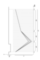
- 11A and 11B are diagrams for explaining an example of an optimization process for a time change pattern of a source frequency.
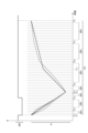
- 11A and 11B are diagrams for explaining an example of an optimization process for a time change pattern of a source frequency.
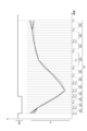
- 11A and 11B are diagrams for explaining an example of an optimization process for a time change pattern of a source frequency.
- FIGS. 11A and 11B are diagrams for explaining an example of an optimization process for a time change pattern of a source frequency.
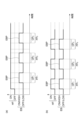
- Each of (a) and (b) of FIG. 9 is a timing chart of an example of the source RF power and the electrical bias.
- Each of (a) and (b) of FIG. 10 is a timing chart of an example of the source high frequency power and the electrical bias.
- Each of (a) to (c) of FIG. 11 is a timing chart of an example of the electrical bias.
- 4 is a flow diagram of a frequency control method according to an exemplary embodiment.
- 1 is a flow diagram illustrating an example of a step STA of a frequency control method according to an exemplary embodiment.
- 1 is a flow diagram illustrating an example of a step STA of a frequency control method according to an exemplary embodiment.
- FIG. 1 is a diagram for explaining an example of the configuration of a plasma processing system.
- the plasma processing system includes a plasma processing device 1 and a control unit 2.
- the plasma processing system is an example of a substrate processing system
- the plasma processing device 1 is an example of a substrate processing device.
- the plasma processing device 1 includes a plasma processing chamber 10, a substrate support unit 11, and a plasma generation unit 12.
- the plasma processing chamber 10 has a plasma processing space.
- the plasma processing chamber 10 also has at least one gas supply port for supplying at least one processing gas to the plasma processing space, and at least one gas exhaust port for exhausting gas from the plasma processing space.
- the gas supply port is connected to a gas supply unit 20 described later, and the gas exhaust port is connected to an exhaust system 40 described later.
- the substrate support unit 11 is disposed in the plasma processing space, and has a substrate support surface for supporting a substrate.
- the plasma generating unit 12 is configured to generate plasma from at least one processing gas supplied into the plasma processing space.
- the plasma formed in the plasma processing space may be capacitively coupled plasma (CCP), inductively coupled plasma (ICP), ECR plasma (Electron-Cyclotron-Resonance Plasma), Helicon Wave Plasma (HWP), or Surface Wave Plasma (SWP), etc.
- the control unit 2 processes computer-executable instructions that cause the plasma processing apparatus 1 to perform the various steps described in this disclosure.
- the control unit 2 may be configured to control each element of the plasma processing apparatus 1 to perform the various steps described herein. In one embodiment, a part or all of the control unit 2 may be included in the plasma processing apparatus 1.
- the control unit 2 may include a processing unit 2a1, a storage unit 2a2, and a communication interface 2a3.
- the control unit 2 is realized, for example, by a computer 2a.
- the processing unit 2a1 may be configured to perform various control operations by reading a program from the storage unit 2a2 and executing the read program. This program may be stored in the storage unit 2a2 in advance, or may be acquired via a medium when necessary.
- the acquired program is stored in the storage unit 2a2, and is read from the storage unit 2a2 by the processing unit 2a1 and executed.
- the medium may be various storage media readable by the computer 2a, or may be a communication line connected to the communication interface 2a3.
- the processing unit 2a1 may be a programmable logic device such as a CPU (Central Processing Unit) or an FPGA (Field-Programmable Gate Array).
- the storage unit 2a2 may include a RAM (Random Access Memory), a ROM (Read Only Memory), a HDD (Hard Disk Drive), an SSD (Solid State Drive), or a combination thereof.
- the communication interface 2a3 may communicate with the plasma processing device 1 via a communication line such as a LAN (Local Area Network).
- FIG. 1 is a diagram for explaining an example of the configuration of a capacitively coupled plasma processing device.
- the capacitively coupled plasma processing apparatus 1 includes a plasma processing chamber 10, a gas supply unit 20, a power supply system 30, and an exhaust system 40.
- the plasma processing apparatus 1 also includes a substrate support unit 11 and a gas inlet unit.
- the gas inlet unit is configured to introduce at least one processing gas into the plasma processing chamber 10.
- the gas inlet unit includes a shower head 13.
- the substrate support unit 11 is disposed in the plasma processing chamber 10.
- the shower head 13 is disposed above the substrate support unit 11. In one embodiment, the shower head 13 constitutes at least a part of the ceiling of the plasma processing chamber 10.
- the plasma processing chamber 10 has a plasma processing space 10s defined by the shower head 13, the sidewall 10a of the plasma processing chamber 10, and the substrate support unit 11.
- the plasma processing chamber 10 is grounded.
- the substrate support unit 11 is electrically insulated from the housing of the plasma processing chamber 10.
- the substrate support 11 includes a main body 111 and a ring assembly 112.
- the main body 111 has a central region 111a for supporting the substrate W and an annular region 111b for supporting the ring assembly 112.
- a wafer is an example of a substrate W.
- the annular region 111b of the main body 111 surrounds the central region 111a of the main body 111 in a plan view.
- the substrate W is disposed on the central region 111a of the main body 111
- the ring assembly 112 is disposed on the annular region 111b of the main body 111 so as to surround the substrate W on the central region 111a of the main body 111. Therefore, the central region 111a is also called a substrate support surface for supporting the substrate W, and the annular region 111b is also called a ring support surface for supporting the ring assembly 112.
- the main body 111 includes a base 1110 and an electrostatic chuck 1111.
- the base 1110 includes a conductive member.
- the electrostatic chuck 1111 is disposed on the base 1110.
- the electrostatic chuck 1111 includes a ceramic member 1111a and an electrostatic electrode 1111b disposed within the ceramic member 1111a.
- the ceramic member 1111a has a central region 111a.
- the ceramic member 1111a also has an annular region 111b.
- other members surrounding the electrostatic chuck 1111 such as an annular electrostatic chuck or an annular insulating member, may have the annular region 111b.
- the ring assembly 112 may be disposed on the annular electrostatic chuck or the annular insulating member, or may be disposed on both the electrostatic chuck 1111 and the annular insulating member.
- the ring assembly 112 includes one or more annular members.
- the one or more annular members include one or more edge rings and at least one cover ring.
- the edge rings are formed of a conductive or insulating material, and the cover rings are formed of an insulating material.
- the substrate support 11 may also include a temperature adjustment module configured to adjust at least one of the electrostatic chuck 1111, the ring assembly 112, and the substrate to a target temperature.
- the temperature adjustment module may include a heater, a heat transfer medium, a flow passage 1110a, or a combination thereof.
- a heat transfer fluid such as brine or a gas flows through the flow passage 1110a.
- the flow passage 1110a is formed in the base 1110, and one or more heaters are disposed in the ceramic member 1111a of the electrostatic chuck 1111.
- the substrate support 11 may also include a heat transfer gas supply configured to supply a heat transfer gas to a gap between the back surface of the substrate W and the central region 111a.
- the shower head 13 is configured to introduce at least one processing gas from the gas supply unit 20 into the plasma processing space 10s.
- the shower head 13 has at least one gas supply port 13a, at least one gas diffusion chamber 13b, and multiple gas inlets 13c.
- the processing gas supplied to the gas supply port 13a passes through the gas diffusion chamber 13b and is introduced into the plasma processing space 10s from the multiple gas inlets 13c.
- the shower head 13 also includes at least one upper electrode.
- the gas introduction unit may include, in addition to the shower head 13, one or more side gas injectors (SGI) attached to one or more openings formed in the side wall 10a.
- SGI side gas injectors
- the gas supply unit 20 may include at least one gas source 21 and at least one flow controller 22.
- the gas supply unit 20 is configured to supply at least one process gas from a respective gas source 21 to the showerhead 13 via a respective flow controller 22.
- Each flow controller 22 may include, for example, a mass flow controller or a pressure-controlled flow controller.
- the gas supply unit 20 may include at least one flow modulation device that modulates or pulses the flow rate of the at least one process gas.
- the exhaust system 40 may be connected to, for example, a gas exhaust port 10e provided at the bottom of the plasma processing chamber 10.
- the exhaust system 40 may include a pressure regulating valve and a vacuum pump. The pressure in the plasma processing space 10s is adjusted by the pressure regulating valve.
- the vacuum pump may include a turbomolecular pump, a dry pump, or a combination thereof.
- FIG. 3 is a diagram showing an example of the configuration of a power supply system in a plasma processing apparatus according to an exemplary embodiment.
- the power supply system 30 includes a high frequency power supply 31 and a bias power supply 32.
- the high frequency power supply 31 constitutes the plasma generating unit 12 of the embodiment.
- the high frequency power supply 31 is configured to generate a source high frequency power HF.
- the source high frequency power HF has a source frequency f S. That is, the source high frequency power HF has a sinusoidal waveform whose frequency is the source frequency f S.
- the source frequency f S may be a frequency within a range of 10 MHz to 150 MHz.
- the high frequency power supply 31 is electrically connected to the high frequency electrode via the matching box 33 and is configured to supply source high frequency power HF to the high frequency electrode.
- the high frequency electrode may be provided in the substrate support 11.
- the high frequency electrode may be at least one electrode provided in the conductive member or ceramic member 1111a of the base 1110. Alternatively, the high frequency electrode may be an upper electrode.
- the source high frequency power HF is supplied to the high frequency electrode, plasma is generated from the gas in the chamber 10.
- the matching circuit 33 has a variable impedance.
- the variable impedance of the matching circuit 33 is set to reduce reflection of the source high frequency power HF from the load.
- the matching circuit 33 can be controlled by, for example, the control unit 2.
- the high frequency power supply 31 may include a signal generator 31g, a D/A converter 31c, and an amplifier 31a.
- the signal generator 31g generates a high frequency signal having a source frequency fS .
- the signal generator 31g may be composed of a programmable logic device such as a programmable processor or a field-programmable gate array (FPGA).
- the signal generator 31g may be composed of a single programmable device 30p together with a signal generator 32g described later, or may be composed of a programmable device separate from the signal generator 32g.
- the output of the signal generator 31g is connected to the input of the D/A converter 31c.
- the D/A converter 31c converts the high frequency signal from the signal generator 31g into an analog signal.
- the output of the D/A converter 31c is connected to the input of the amplifier 31a.
- the amplifier 31a amplifies the analog signal from the D/A converter 31c to generate the source high frequency power HF.
- the gain of the amplifier 31a is specified by the control unit 2 to the high frequency power source 31. Note that the high frequency power source 31 does not need to include the D/A converter 31c.
- the output of the signal generator 31g is connected to the input of the amplifier 31a, and the amplifier 31a amplifies the high frequency signal from the signal generator 31g to generate the source high frequency power HF.
- the bias power supply 32 is electrically coupled to the substrate support 11.
- the bias power supply 32 is electrically connected to a bias electrode in the substrate support 11 and is configured to supply an electric bias EB to the bias electrode.
- the bias electrode may be at least one electrode provided in the conductive member or ceramic member 1111a of the base 1110.
- the bias electrode may be common to the radio frequency electrode.
- FIG. 4(a) and 4(b) are diagram showing an example of an electric bias waveform.
- the bias power supply 32 is configured to periodically apply an electric bias EB having a waveform period CY to the bias electrode. That is, the electric bias EB is applied to the bias electrode in each of a plurality of waveform periods CY, which are repetitions of the waveform period CY.
- the waveform period CY is determined by the bias frequency.
- the bias frequency is, for example, a frequency not less than 50 kHz and not more than 27 MHz.
- the time length of the waveform period CY is the reciprocal of the bias frequency.
- the electric bias EB may be bias high frequency power LF having a bias frequency. That is, the electric bias EB may have a sinusoidal waveform whose frequency is the bias frequency.
- the bias power supply 32 is electrically connected to the bias electrode via a matching device 34.
- the variable impedance of the matching device 34 is set to reduce the reflection of the bias high frequency power LF from the load.
- the electric bias EB may include a voltage pulse VP.
- the voltage pulse VP is applied to the bias electrode within a waveform period CY.
- the voltage pulse VP is applied to the bias electrode periodically at a time interval the same as the time length of the waveform period CY.
- the waveform of the voltage pulse VP may be a square wave, a triangular wave, or any other waveform.
- the polarity of the voltage of the voltage pulse VP is set so that a potential difference is generated between the substrate W and the plasma to attract ions from the plasma to the substrate W.
- the voltage pulse VP is applied to the bias electrode so that the waveform period CY includes a period during which the potential of the substrate W is negative.
- the voltage pulse VP applied to the bias electrode may have a negative potential, a positive potential, or a potential that changes between a positive potential and a negative potential.
- the voltage pulse VP may be a negative voltage pulse or a negative DC voltage pulse.
- the plasma processing apparatus 1 does not need to include a matching unit 34.
- the bias power supply 32 may include a signal generator 32g, a D/A converter 32c, and an amplifier 32a, as shown in FIG. 3.
- the signal generator 32g periodically generates a bias signal having a specified waveform and waveform period CY.
- the signal generator 32g may be comprised of a programmable processor or a programmable logic device such as an FPGA.
- the output of the signal generator 32g is connected to the input of the D/A converter 32c.
- the D/A converter 32c converts the bias signal from the signal generator 32g into an analog signal.
- the output of the D/A converter 32c is connected to the input of the amplifier 32a.
- the amplifier 32a amplifies the analog signal from the D/A converter 32c to generate the electric bias EB.
- the gain of the amplifier 32a is specified by the control unit 2 to the bias power supply 32.
- the bias power supply 32 does not need to include the D/A converter 32c.
- the output of the signal generator 32g is connected to the input of the amplifier 32a, and the amplifier 32a amplifies the bias signal from the signal generator 32g to generate the electric bias EB.
- the bias power supply 32 may periodically generate the voltage pulse VP by periodically switching its output voltage between the output voltage of the high voltage power supply and the ground potential or another potential.
- the high frequency power supply 31 is configured to specify an optimal time-varying pattern of the source frequency fS in the waveform period CY that most suppresses the degree of reflection of the source high frequency power HF by changing the source frequency fS in the time series of the multiple waveform periods CY.
- the process of specifying the optimal time-varying pattern of the source frequency fS is referred to as an "optimization process".
- the high frequency power supply 31 may set the source frequency fS at multiple discrete time points (phases) in each waveform period CY in the time series.
- the high frequency power supply 31 may set the source frequency fS continuously in time in each waveform period CY in the time series of the multiple waveform periods CY.
- the calculation of the optimization process may be performed in the signal generator 31g of the high frequency power supply 31.
- the calculation of the optimization process may be performed by the control unit 2.
- the plasma processing apparatus 1 may further include a sensor 35 and/or a sensor 36 (see FIG. 2) to determine the degree of reflection of the source high frequency power HF in the optimization process.
- the sensor 35 is configured to measure the power level Pr of the reflected wave of the source high frequency power HF from the load.
- the sensor 35 includes, for example, a directional coupler.
- the directional coupler may be provided between the high frequency power supply 31 and the matching device 33.
- the sensor 35 may further be configured to measure the power level Pf of the traveling wave of the source high frequency power HF.
- the power level Pr of the reflected wave measured by the sensor 35 is notified to the high frequency power supply 31.
- the power level Pf of the traveling wave may be notified from the sensor 35 to the high frequency power supply 31.
- the sensor 36 includes a voltage sensor and a current sensor.
- the sensor 36 is configured to measure a voltage V S and a current I S in a power supply path that connects the high frequency power supply 31 and the high frequency electrode to each other.
- the source high frequency power HF is supplied to the high frequency electrode via this power supply path.
- the sensor 36 may be provided between the high frequency power supply 31 and the matching unit 33. The voltage V S and the current I S are notified to the high frequency power supply 31.
- the high frequency power supply 31 generates a representative value from the notified measured value.
- the measured value may be the power level Pr of the reflected wave acquired by the sensor 35.
- the measured value may be the ratio value of the power level Pr of the reflected wave to the output power level of the source high frequency power HF (i.e., the reflectance).
- the measured value may be the phase difference ⁇ between the voltage V S and the current I S acquired by the sensor 36.
- the measured value may be the impedance Z L of the load side of the high frequency power supply 31 in each of the multiple phase periods SP.
- the impedance Z L is determined from the voltage V S and the current I S acquired by the sensor 36.
- the measured value may be a reflection coefficient calculated from the impedance Z L and the output impedance of the high frequency power supply 31.
- the representative value represents the degree of reflection of the source high frequency power HF in each waveform period CY.
- the representative value may be the average value or maximum value of the measured value in each waveform period CY.
- the representative value may be the average value or maximum value of the measured value in a part of the period in which the source frequency f S is changed in each waveform period CY.
- FIG. 5 to 8 is a diagram for explaining an example of optimization process of the time change pattern of the source frequency.
- the optimization processes include, in order, a first optimization process, ..., a Jth optimization process.
- J may be any integer equal to or greater than 2. In the example illustrated in Figures 5 to 7, J is 3.
- the high frequency power source 31 searches for an optimal time change pattern in a time series of a plurality of waveform periods CY.
- the high frequency power source 31 uses an initial time pattern of the source frequency fS prepared in advance as the time pattern of the source frequency fS of the initial waveform period CY in the time series.
- the high frequency power supply 31 performs a first optimization process.
- the high frequency power supply 31 identifies a first time change pattern of the source frequency fS in the waveform period CY that most effectively suppresses the degree of reflection of the source high frequency power HF.
- the high frequency power supply 31 uses a time change pattern of the source frequency fS that includes the source frequency fS at each of the multiple first time points (phases) within each waveform period CY in the time series and the interpolated source frequency fS in each of the multiple first divided periods DP1 .
- the number of the multiple first time points in each waveform period CY is two or more.
- the multiple first time points include time points T11 to T13 .
- the waveform period CY is divided into multiple first divided periods DP1 by the multiple first time points.
- the multiple first divided periods DP1 include the period between time points T11 and T12 , the period between time points T12 and T13 , and the period between time points T13 and the final time point T E in the waveform period CY.
- the source frequency fS at the initial first time point T11 and the source frequency fS at the final time point T E in the waveform period CY are the same.
- the first points in time (phases) in each waveform period CY may be determined in advance.
- the first points in time may be set such that each of the first divided periods DP1 has a first change amount as a change amount of the load impedance of the high frequency power supply 31 with respect to the above-mentioned initial time pattern.
- the first points in time may be set such that each of the first divided periods DP1 has a first change amount as a change amount of the source frequency with respect to the above-mentioned initial time pattern.
- the first points in time may be set such that the section in the waveform period CY in which the load impedance of the high frequency power supply 31 or the degree of reflection of the source high frequency power HF is larger is divided into a larger number of divided periods.
- the electric bias EB includes a voltage pulse VP
- the first points in time may be set such that the section in the waveform period CY in which the change amount of the voltage at the substrate support 11 in response to the voltage pulse VP is larger is divided into a larger number of divided periods.
- one of the plurality of first divided periods DP1 may include a period during which the voltage pulse VP is supplied to the substrate support portion 11.
- the high frequency power supply 31 changes the time change pattern of the source frequency fS of the waveform period CYm in the time series from the time change pattern of the source frequency fS in the preceding waveform period CYm -M1 . Specifically, the high frequency power supply 31 sequentially changes the source frequency fS of each of the multiple first time points in the time series of the multiple waveform periods CY.
- the high frequency power supply 31 sets the source frequency fS [m, T1n ] of the first time point T1n in the waveform period CYm in the time series to a frequency having one change with respect to the source frequency fS [m-M1, T1n ] of the first time point T1n in the preceding waveform period CYm -M1 .
- the one change is a decrease or increase in frequency.
- "m” is a natural number representing the order of the waveform period CY in the time series.
- n is a natural number representing the order of each of the multiple first time points in the waveform period CY.
- M1 is an integer equal to or greater than 1, for example, 1.
- f S [m, T 1n ] represents the source frequency f S at the first time point T 1n within the waveform period CY m .
- the high frequency power supply 31 interpolates the source frequency fS in each of the multiple first divided periods DP1 from the source frequency fS at the immediately preceding time point among the multiple first time points and time points T1E and the source frequency fS at the immediately succeeding time point.
- the high frequency power supply 31 may use linear interpolation in the interpolation of the source frequency fS .
- the high frequency power supply 31 may use interpolation by a higher order equation in the interpolation of the source frequency fS . Note that the example shown in FIG. 5 shows a situation in which the source frequency fS at the first time point T12 is changed.
- the high frequency power source 31 sets the source frequency fs [m+M1, T1n ] in the subsequent waveform period CYm +M1 in the time series to a frequency having one change with respect to the source frequency fs [m, T1n ].
- the high frequency power source 31 sets the frequency fs [m+M1, T1n ] in the subsequent waveform period CYm +M1 in the time series to a frequency having the other change with respect to the source frequency fs [m, T1n ].
- the other change is a decrease or increase in frequency, which is the opposite change to the one change.
- the high frequency power supply 31 may sequentially optimize the source frequency f S at each of the multiple first time points so as to suppress the degree of reflection of the source high frequency power HF.
- the high frequency power supply 31 may specify the first time change pattern by repeatedly adjusting (or changing) the source frequency f S at each of the multiple first time points in sequence.
- the order of the time points at which the source frequency f S is optimized or adjusted among the multiple first time points may be predetermined or may be any order.
- the source frequency f S may be optimized or adjusted in order from the time point at which it is empirically known that the change in the source frequency f S at that time point has a large effect on the degree of reflection among the multiple first time points.
- the high frequency power supply 31 specifies, as a first time change pattern, a time change pattern of the source frequency fS of the waveform period CY when the degree of reflection of the source high frequency power HF satisfies a first condition.
- the first condition is predetermined as a condition indicating that the degree of reflection of the source high frequency power HF is sufficiently suppressed.
- the first condition may be satisfied when the degree of reflection of the source high frequency power HF is included in a first allowable range.
- the initial time pattern is indicated by a solid line
- the time change pattern used in the first optimization process is indicated by a dashed line.
- the high frequency power source 31 performs a second optimization process after the first optimization process.
- the high frequency power source 31 specifies a second time change pattern of the source frequency fS in the waveform period CY that most suppresses the degree of reflection of the source high frequency power HF based on the first reference pattern.
- the first reference pattern is the first time change pattern or a first derived time pattern of the source frequency fS generated from the first time change pattern.
- the high frequency power supply 31 uses a time change pattern of the source frequency fS that includes the source frequency fS at each of the multiple second time points (phases) within each waveform period CY in the time series and the interpolated source frequency fS in each of the multiple second divided periods DP2 .
- the number of the second time points in each waveform period CY is greater than the number of the first time points in each waveform period CY in the first optimization process.
- the second time points include time points T21 to T27 .
- the waveform period CY is divided into a plurality of second divided periods DP2 by the second time points.
- the number of the second divided periods DP2 in each waveform period CY is greater than the number of the first divided periods DP1 in the waveform period CY in the first optimization process.
- the multiple second division periods DP2 include a period between time T21 and time T22 , a period between time T22 and time T23 , a period between time T23 and time T24 , a period between time T24 and time T25 , a period between time T25 and time T26 , a period between time T26 and time T27 , and a period between time T27 and a final time T E in the waveform period CY.
- the source frequency fS at the first second time T21 and the source frequency fS at the final time T E in the waveform period CY are the same.
- the second time points (phases) in each waveform period CY may be determined in advance.
- the second time points may be set such that each of the second divided periods DP2 has a second change amount as the change amount of the load impedance of the high frequency power supply 31 with respect to the above-mentioned first reference pattern. In this case, the second change amount is smaller than the first change amount.
- the second time points may be set such that each of the second divided periods DP2 has a second change amount as the change amount of the source frequency with respect to the first reference pattern. In this case, the second change amount is also smaller than the first change amount.
- the second time points may be set such that the section in the waveform period CY has a larger load impedance of the high frequency power supply 31 or a larger degree of reflection of the source high frequency power HF, so that the second time points are divided into a larger number of divided periods.
- the electric bias EB includes a voltage pulse VP
- the second time points may be set such that the section in the waveform period CY has a larger change amount of the voltage at the substrate support 11 in response to the voltage pulse VP, so that the second time points are divided into a larger number of divided periods.
- the second points in time may include points in time that are the same as the first points in time within the waveform period CY.
- the high frequency power supply 31 changes the time change pattern of the source frequency fS of the waveform period CYm in the time series from the time change pattern of the source frequency fS in the preceding waveform period CYm -M2 .
- the time change pattern of the source frequency fS of the waveform period CY is obtained by changing the first reference pattern.
- the high frequency power supply 31 sequentially changes the source frequency fS at each of the multiple second time points in the time series of the multiple waveform periods CY. More specifically, in the second optimization process, the high frequency power supply 31 sets the source frequency fS [m, T2n ] at the second time point T2n in the waveform period CYm in the time series to a frequency having one change with respect to the source frequency fS [m-M2, T2n ] at the second time point T2n in the preceding waveform periphery CYm-M2 .
- the one change is a decrease or increase in frequency.
- "m" is a natural number representing the order of the waveform period CY in the time series.
- n is a natural number representing the order of each of the multiple second time points in the waveform period CY.
- M2 is an integer equal to or greater than 1, for example, 1.
- fS [m, T2n ] represents the source frequency fS at the second time point T2n in the waveform period CYm .
- the high frequency power supply 31 interpolates the source frequency fS in each of the second divided periods DP2 from the source frequency fS at the immediately preceding time point and the source frequency fS at the immediately succeeding time point among the second time points and the time point TE .
- the high frequency power supply 31 may use linear interpolation in the interpolation of the source frequency fS .
- the high frequency power supply 31 may use interpolation using a higher order equation in the interpolation of the source frequency fS .
- the high frequency power source 31 sets the source frequency fs [m+M2, T2n ] in the subsequent waveform period CYm +M2 in the time series to a frequency having one change with respect to the source frequency fs [m, T2n ].
- the high frequency power source 31 sets the frequency fs [m+M2, T2n ] in the subsequent waveform period CYm +M2 in the time series to a frequency having the other change with respect to the source frequency fs [m, T2n ].
- the other change is a decrease or increase in frequency, which is the opposite change to the one change.
- the high frequency power supply 31 may sequentially optimize the source frequency f S at each of the plurality of second time points so as to suppress the degree of reflection of the source high frequency power HF.
- the high frequency power supply 31 may specify the second time-varying pattern by repeatedly adjusting (or changing) the source frequency f S at each of the plurality of second time points in sequence.
- the order of the time points at which the source frequency f S is optimized or adjusted among the plurality of second time points may be predetermined or may be any order.
- the source frequency f S may be optimized or adjusted in order from the time point at which it is empirically known that the change in the source frequency f S at that time point has a large effect on the degree of reflection among the plurality of second time points.
- the high frequency power supply 31 specifies, as the second time change pattern, the time change pattern of the source frequency fS of the waveform period CY when the degree of reflection of the source high frequency power HF satisfies the second condition.
- the second condition is predetermined as a condition indicating that the degree of reflection of the source high frequency power HF is sufficiently suppressed.
- the second condition may be satisfied when the degree of reflection of the source high frequency power HF is included in a second allowable range.
- the first reference pattern is indicated by a solid line
- the time change pattern used in the second optimization process is indicated by a dashed line.
- the high frequency power supply 31 may further perform a third optimization process after the second optimization process. Furthermore, the high frequency power supply 31 may further perform a fourth optimization process after the third optimization process.
- "j" is used as the symbol indicating the order of each optimization process, and the jth optimization process representing each of the second optimization process to the Jth optimization process will be described.
- the high frequency power supply 31 specifies the jth time change pattern of the source frequency fS in the waveform period CY that most suppresses the degree of reflection of the source high frequency power HF, based on the (j-1)th reference pattern.
- the (j-1)th reference pattern is the (j-1)th time change pattern or the (j-1)th derived time pattern of the source frequency fS generated from the (j-1)th time change pattern.
- the high-frequency power supply 31 uses a time change pattern of the source frequency fS that includes the source frequency fS at each of the multiple jth time points (phases) in each waveform period CY in the time series and the interpolated source frequency fS in each of the multiple jth divided periods DPj .
- the number of the jth time points in each waveform period CY is greater than the number of the jth time points in each waveform period CY in the (j-1)th optimization process.
- the waveform period CY is divided into jth divided periods DPj by the jth time points.
- the number of the jth divided periods DPj in each waveform period CY is greater than the number of the (j-1)th divided periods DP (j-1) in the waveform period CY in the (j-1 )th optimization process.
- the source frequency fS at the first jth time point Tj1 and the source frequency fS at the final time point T E in the waveform period CY are the same.
- the third time points include time points T31 to T3b .
- the third division periods DP3 include a period between time points T31 and T32 , a period between time points T32 and T33 , a period between time points T33 and T34 , a period between time points T34 and T35 , a period between time points T35 and T36 , a period between time points T36 and T37 , a period between time points T37 and T38 , a period between time points T37 and T38 , a period between time points T38 and T39 , a period between time points T39 and T3a , a period between time points T3a and T3b , and a period between time points T3b and the final time point T3E in the waveform period CY.
- the source frequency fS at the first third time point T31 and the source frequency fS at the final time point T3E in the waveform period CY are the same.
- the jth time points (phases) in each waveform cycle CY may be determined in advance.
- the jth time points may be set such that each of the jth divided periods DPj has the jth change amount as the change amount of the load impedance of the high frequency power supply 31 with respect to the (j-1)th reference pattern described above. In this case, the jth change amount is smaller than the (j-1) change amount.
- the jth time points may be set such that each of the jth divided periods DPj has the jth change amount as the change amount of the source frequency with respect to the (j-1)th reference pattern. In this case, the jth change amount is also smaller than the (j-1) change amount.
- the jth time points may be set such that the section in the waveform cycle CY in which the load impedance of the high frequency power supply 31 or the degree of reflection of the source high frequency power HF is larger is divided into a larger number of divided periods.
- the electric bias EB includes a voltage pulse VP
- the jth time points may be set so that the section within the waveform period CY is divided into a greater number of divided periods in which the voltage change amount at the substrate support portion 11 in response to the voltage pulse VP is greater.
- the jth time points may include a plurality of time points within the waveform period CY that are the same as the (j-1)th time points, respectively.
- the high frequency power supply 31 changes the time change pattern of the source frequency fS of the waveform period CYm in the time series from the time change pattern of the source frequency fS in the preceding waveform period CYm-Mj .
- the time change pattern of the source frequency fS of the waveform period CY is obtained by changing the (j-1)th reference pattern.
- the high frequency power supply 31 sequentially changes the source frequency fS at each of the multiple j-th time points in the time series of the multiple waveform periods CY. More specifically, in the j-th optimization process, the high frequency power supply 31 sets the source frequency fS [m, Tjn ] at the j-th time point Tjn in the waveform period CYm in the time series to a frequency having one change with respect to the source frequency fS [m-Mj, Tjn ] at the j-th time point Tjn in the preceding waveform periphery CYm -Mj . The one change is a decrease or increase in frequency. "m" is a natural number representing the order of the waveform period CY in the time series.
- n is a natural number representing the order of each of the multiple j-th time points in the waveform period CY.
- Mj is an integer equal to or greater than 1, for example, 1.
- fS [m, Tjn ] represents the source frequency fS at the j-th time point Tjn in the waveform period CYm .
- the high frequency power supply 31 interpolates the source frequency f S in each of the multiple j-th divided periods DP j from the source frequency f S at the immediately preceding time point and the source frequency f S at the immediately succeeding time point among the multiple j-th time points and the time point T E.
- the high frequency power supply 31 may use linear interpolation in the interpolation of the source frequency f S.
- the high frequency power supply 31 may use interpolation using a higher order equation in the interpolation of the source frequency f S.
- the high frequency power source 31 sets the source frequency fS [m+Mj, Tjn ] in the subsequent waveform period CYm +Mj in the time series to a frequency having one of the changes with respect to the source frequency fS [m, Tjn ].
- the high frequency power source 31 sets the frequency fS [m+Mj, Tjn ] in the subsequent waveform period CYm +Mj in the time series to a frequency having the other change with respect to the source frequency fS [m, Tjn ].
- the other change is a decrease or increase in frequency, which is the opposite change to the one change.
- the high frequency power supply 31 may sequentially optimize the source frequency fS at each of the jth time points so as to suppress the degree of reflection of the source high frequency power HF.
- the high frequency power supply 31 may specify the jth time-varying pattern by repeatedly adjusting (or changing) the source frequency fS at each of the jth time points in sequence.
- the order of the time points at which the source frequency fS is optimized or adjusted among the jth time points may be predetermined or may be any order.
- the source frequency fS may be optimized or adjusted in order from the time points at which it is empirically known that the change in the source frequency fS at that time point has a large effect on the degree of reflection among the jth time points.
- the high frequency power supply 31 specifies the time change pattern of the source frequency fS of the waveform period CY when the degree of reflection of the source high frequency power HF satisfies the jth condition as the jth time change pattern.
- the jth condition is predetermined as a condition indicating that the degree of reflection of the source high frequency power HF is sufficiently suppressed.
- the jth condition may be satisfied when the degree of reflection of the source high frequency power HF is included in the jth allowable range.
- the third reference pattern is indicated by a solid line
- the time change pattern used in the third optimization process is indicated by a dashed line.
- the high frequency power supply 31 uses the time change pattern obtained by the final optimization process that most suppresses the degree of reflection within the waveform period CY as the optimal time change pattern, and can use this pattern in the subsequent waveform period CY in the time series.
- the high frequency power supply 31 may perform the first optimization process again if the degree of reflection of the source high frequency power HF becomes so large that it does not satisfy the predetermined condition while performing the jth optimization process (j is an integer equal to or greater than 2). Thereafter, the high frequency power supply 31 may further perform the second to Jth optimization processes. According to this embodiment, if an abnormal plasma discharge occurs during the jth optimization process, it becomes possible to search again for a time change pattern of the source frequency HF that suppresses the degree of reflection of the source high frequency power HF within the waveform period CY.
- the high frequency power supply 31 may obtain the (j-1)th derived time pattern of the source frequency fS from the (j-1)th time change pattern after the (j-1)th optimization process and before the jth optimization process.
- the high frequency power supply 31 shifts the (j-1)th time change pattern in the time direction in multiple waveform periods CY in the time series.
- the minimum amount of shift in the time direction may be smaller than the time pitch of multiple discrete time points at which the source frequency is set in the waveform period CY.
- the high frequency power supply 31 may identify, as the (j-1)th derived time pattern, the time change pattern that most suppresses the degree of reflection of the source high frequency power HF in the waveform period CY, among the multiple time change patterns obtained by shifting the (j-1)th time change pattern in the time direction.
- the (j-1)th derived time pattern may be used as the (j-1)th reference pattern in the jth optimization process.
- the high frequency power supply 31 obtains a derived time pattern of the source frequency fS from the first time change pattern after the first optimization process and before the second optimization process.
- the high frequency power supply 31 shifts the first time change pattern in the time direction in a plurality of waveform periods CY in the time series.
- the high frequency power supply 31 may specify, as the first derived time pattern, a time change pattern that most suppresses the degree of reflection of the source high frequency power HF among a plurality of time change patterns obtained by shifting the first time change pattern in the time direction.
- the first derived time pattern may be used as a first reference pattern in the second optimization process.
- the solid line indicates the first time change pattern
- the dashed line indicates a plurality of time change patterns obtained by shifting the first time change pattern in the time direction.
- the above-described process of identifying a time change pattern that suppresses reflections by shifting the time change pattern of the source frequency f S in the waveform period CY in the time direction may be used at any timing in each of the first to Jth optimization processes.
- the source high frequency power HF and the electric bias EB are supplied simultaneously and continuously. That is, in one embodiment, a continuous wave of the source high frequency power HF and a continuous wave of the electric bias EB are supplied simultaneously.
- a first process which is one type of the optimization process described above, is applied. In the first process, the optimization process described above is applied to multiple consecutive waveform periods CY as multiple waveform periods CY in the time series described above.
- the bias power supply 32 periodically supplies a pulse EBP of an electric bias EB to the bias electrode.
- the pulse EBP is supplied to the bias electrode in each of a plurality of pulse periods PP.
- Each of the plurality of pulse periods PP includes a repetition of a waveform period CY. That is, in each of the plurality of pulse periods PP, the electric bias EB is periodically supplied to the bias electrode.
- FIG. 9(a), FIG. 9(b), FIG. 10(a), and FIG. 10(b) is a timing chart of an example of source high frequency power HF and electric bias EB.
- “ON” of source high frequency power HF indicates that source high frequency power HF is being supplied
- “OFF” of source high frequency power HF indicates that the supply of source high frequency power HF is stopped.
- “ON” of electric bias EB indicates that electric bias EB is being applied to the bias electrode
- “OFF” of electric bias EB indicates that electric bias EB is not being applied to the bias electrode.
- “HIGH” of electric bias EB indicates that electric bias EB having a level higher than the level of electric bias EB indicated by "LOW” is being applied to the bias electrode.
- the multiple pulse periods PP appear in sequence in time.
- the multiple pulse periods PP appear in sequence at time intervals (periods) that are the inverse of the pulse frequency.
- a pulse period PP k represents the kth pulse period among the multiple pulse periods PP.
- the pulse frequency is lower than the bias frequency, and is, for example, a frequency of 1 kHz or more and 100 kHz or less.
- the electric bias EB is periodically applied to the bias electrode in each of the multiple pulse periods PP. In periods other than the multiple pulse periods PP, the electric bias EB may not be applied to the bias electrode. Alternatively, an electric bias EB having a level lower than the level of the electric bias EB in the multiple pulse periods PP may be applied to the bias electrode in periods other than the multiple pulse periods PP.
- the source radio frequency power HF may be supplied as a continuous wave.
- a pulse of the source high frequency power HF may be supplied.
- a pulse of the source high frequency power HF may be supplied in each of a plurality of periods that respectively coincide with a plurality of pulse periods PP.
- a pulse of the source high frequency power HF may be supplied in each of a plurality of periods that respectively partially overlap with a plurality of pulse periods PP.
- each of a plurality of overlap periods OP in which the source high frequency power HF and the electric bias EB are supplied simultaneously is a part of a corresponding pulse period PP among the plurality of pulse periods PP.
- an overlap period OP k represents a k-th overlap period among the plurality of overlap periods OP.
- a waveform period CY m represents the m-th waveform period among the multiple waveform periods CY in each of the multiple overlap periods OP.
- Figs. 11(a) to 11(c) are timing chart of an example of the electric bias.
- the high frequency power supply 31 uses a previously prepared initial time pattern as the time pattern of the source frequency fS of each of the waveform periods CY1 to CYMa in each of the overlap periods OP1 to OPKa , where Ka is an integer equal to or greater than 1, for example, 5. Ma is also an integer equal to or greater than 1.
- the high frequency power supply 31 performs a first process on the waveform periods CY Ma+1 to CY M in each of the overlap periods OP 1 to OP Ka as a time series of a plurality of consecutive waveform periods CY.
- each of the multiple time series includes waveform periods CY m in the same order among waveform periods CY 1 to CY Mb in each of the overlapping periods OP Ka+1 to the final overlapping period. That is, the multiple time series include the first to Mb-th time series. Mb is an integer of 1 or more.
- Each of the multiple time series includes multiple waveform periods CY. Specifically, the first time series includes waveform period CY 1 in each of the overlapping periods OP Ka+1 to the final overlapping period. The second time series includes waveform period CY 2 in each of the overlapping periods OP Ka+1 to the final overlapping period.
- the Mb-th time series includes waveform period CY Mb in each of the overlapping periods OP Ka+1 to the final overlapping period.
- each of the multiple time series is a time series of multiple waveform periods CY to which the above-mentioned optimization processes (ie, the first optimization process to the Jth optimization process) are applied.
- the high frequency power supply 31 applies the above-described first process to the waveform period CY Mb +1 to the waveform period CY M in each of the overlap period OP Ka+1 to the final overlap period as a time series of a plurality of consecutive waveform periods CY.
- the plasma processing apparatus 1 described above it is possible to reduce the degree of reflection of the source high frequency power HF in the waveform period CY. Also, according to the plasma processing apparatus 1, it is possible to smoothly change the source frequency fS in each waveform period CY so as to suppress the degree of reflection of the source high frequency power HF.
- FIG. 12 is a flow chart of a frequency control method according to one exemplary embodiment.
- FIG. 13 and 14 is a flow chart showing an example of step STA of a frequency control method according to one exemplary embodiment.
- the frequency control method shown in Figure 12 (hereinafter referred to as "method MT") can be performed using a plasma processing apparatus 1.
- method MT each part of the plasma processing apparatus 1 can be controlled by a control unit 2.
- the method MT begins with step STA, in which a source high frequency power HF is supplied from the high frequency power supply 31 to generate plasma from the gas in the chamber 10.
- step STB an electrical bias EB is supplied to the bias electrode of the substrate support 11. Step STA is performed when step STB is being performed.
- step STa of process STA in one or several initial waveform periods CY in the time series of multiple waveform periods CY, the above-mentioned initial time pattern is used as the time pattern of the source frequency fS .
- a first optimization process is performed. As described above, in the first optimization process, the source frequency f S at each of the first time points in the time series of the waveform periods CY is changed, and the source frequency f S at each of the first time points and the interpolated source frequency in each of the first divided periods DP1 are used.
- step STb as described above for the first optimization process, the time change pattern of the source frequency fS of the waveform period CYm in the time series is changed from the time change pattern of the source frequency fS in the preceding waveform period CYm -M1 .
- step STJa it is determined whether the degree of reflection of the source high frequency power HF satisfies the first condition described above. If the first condition is not satisfied, step STb is performed again. If the first condition is satisfied, the time change pattern finally obtained in the first optimization process is identified as the above-mentioned first time change pattern in step STc.
- the method MT may include a step STd that is performed after the first optimization process and before the second optimization process.
- step STd as described above, a time change pattern that most effectively suppresses the degree of reflection of the source high frequency power HF is identified as a first derived time pattern from a plurality of time change patterns obtained by shifting the first time change pattern in the time direction.
- the second optimization process is performed. As described above, in the second optimization process, the source frequency f S at each of the second time points in the time series of the waveform periods CY is changed, and the source frequency f S at each of the second time points and the interpolated source frequency in each of the second divided periods DP2 are used.
- step STe as described above for the second optimization process, the time change pattern of the source frequency fS of the waveform period CYm in the time series is changed from the time change pattern of the source frequency fS in the preceding waveform period CYm-M2 .
- the time change pattern of the source frequency fS of the waveform period CY is obtained by changing the first reference pattern.
- a step STJb may be performed.
- the step STJb it is determined whether the degree of reflection of the source high frequency power HF becomes so large that it does not satisfy a predetermined condition by using the time change pattern of the changed source frequency fS in the waveform period CYm . If it is determined that the degree of reflection of the source high frequency power HF becomes so large that it does not satisfy a predetermined condition by using the time change pattern of the changed source frequency fS in the waveform period CYm as a result of the determination in STJb, the process returns to the step STa.
- the process proceeds to the step STJc.
- step STJc it is determined whether the degree of reflection of the source high frequency power HF satisfies the second condition described above. If the second condition is not satisfied, step STe is performed again. If the second condition is satisfied, the time change pattern finally obtained in the second optimization process is identified as the second time change pattern described above in step STf.
- the method MT may further include steps STg to STh.
- steps STg to STh a third optimization process is performed. As described above, in the third optimization process, the source frequency f S at each of the third time points in the time series is changed, and the source frequency f S at each of the third time points and the interpolated source frequency in each of the third divided periods DP3 are used.
- step STg as described above for the third optimization process, the time change pattern of the source frequency fS of the waveform period CYm in the time series is changed from the time change pattern of the source frequency fS in the preceding waveform period CYm-M3 .
- the time change pattern of the source frequency fS of the waveform period CY is obtained by changing the second reference pattern.
- a step STJd may be performed.
- the step STJd it is determined whether the degree of reflection of the source high frequency power HF becomes so large that it does not satisfy a predetermined condition by using the time change pattern of the changed source frequency fS in the waveform period CYm . If it is determined that the degree of reflection of the source high frequency power HF becomes so large that it does not satisfy a predetermined condition by using the time change pattern of the changed source frequency fS in the waveform period CYm as a result of the determination in STJd, the process returns to the step STa.
- the process proceeds to the step STJe.
- step STJe it is determined whether the degree of reflection of the source high frequency power HF satisfies the third condition described above. If the third condition is not satisfied, step STg is performed again. If the third condition is satisfied, the time change pattern finally obtained in the third optimization process is identified as the third time change pattern described above in step STh.
- Method MT may end after step STh.
- method MT may further include fourth through Jth optimization processes as described above.
- fourth through Jth optimization processes please refer to the explanation of the jth optimization process described above.
- the plasma processing apparatus may be an inductively coupled plasma processing apparatus, an ECR plasma processing apparatus, a helicon wave excited plasma processing apparatus, or a surface wave plasma processing apparatus.
- a source high frequency power HF is used to generate the plasma.
- a chamber a substrate support disposed within the chamber; a radio frequency power source configured to provide a source radio frequency power to generate a plasma from a gas in the chamber; a bias power supply configured to supply an electrical bias having a waveform period to the substrate support; Equipped with The high frequency power source is While changing a source frequency of the source high frequency power at each of a plurality of first time points within the waveform period, a first time change pattern of the source frequency in the waveform period that most suppresses a degree of reflection of the source high frequency power is identified using the source frequency at each of the plurality of first time points and an interpolated source frequency within each of a plurality of first divided periods of the waveform period divided by the plurality of first time points; changing a source frequency of the source high frequency power at each of a plurality of second time points in the waveform period relative to the first time change pattern or a time change pattern of the source frequency created from the first time change pattern, and using the source frequency at each of the plurality of second time points and an inter
- the high frequency power source is optimizing the source frequency at each of the first points in time in sequence to reduce a degree of reflection of the source radio frequency power in order to identify the first time-varying pattern; optimizing the source frequency for each of the second points in time in sequence to reduce a degree of reflection of the source high frequency power in order to identify the second time-varying pattern; It is configured as follows: The plasma processing apparatus according to E1.
- the high frequency power source is repeatedly adjusting the source frequency at each of the first points in time in sequence to identify the first time-varying pattern; repeating the step of sequentially adjusting the source frequency for each of the plurality of second time points to identify the second time-varying pattern. It is configured as follows: The plasma processing apparatus according to E1.
- the plurality of first time points are set such that each of the plurality of first divided periods has a first amount of change as an amount of change in load impedance of the high frequency power source with respect to a time change pattern of the source frequency in the waveform period initially used for identifying the first time change pattern, the plurality of second time points are set such that each of the plurality of second divided periods has a second change amount as a change amount of the load impedance of the high frequency power supply with respect to the first time change pattern or a time change pattern of the source frequency created from the first time change pattern;
- the plasma processing apparatus according to any one of E1 to E3.
- the plurality of first time points are set such that each of the plurality of first divided periods has a first amount of change as an amount of change in the source frequency with respect to a time change pattern of the source frequency in the waveform period initially used to identify the first time change pattern;
- the plurality of second time points are set such that each of the plurality of second divided periods has a second change amount as a change amount of the source frequency with respect to the first time change pattern or the time change pattern created from the first time change pattern.
- the plurality of first time points and the plurality of second time points are set so that a section within the waveform period is divided into a greater number of divided periods as the load impedance of the high frequency power source or the degree of reflection of the source high frequency power increases.
- the plasma processing apparatus according to any one of E1 to E3.
- the electrical bias is a bias high frequency power having the waveform period, or includes a voltage pulse generated at a time interval equal to the time length of the waveform period.
- the plasma processing apparatus according to any one of E1 to E9.
- the electrical bias includes voltage pulses generated at time intervals equal to the time length of the waveform period; the plurality of first time points and the plurality of second time points are set such that a section within the waveform period is divided into a greater number of divided periods as the section has a greater amount of change in voltage at the substrate support part in response to the voltage pulse.
- the plasma processing apparatus according to any one of E1 to E3.
- the electrical bias includes voltage pulses generated at time intervals equal to the time length of the waveform period; one of the plurality of first divided periods includes a period during which the voltage pulse is supplied to the substrate support;
- the plasma processing apparatus according to any one of E1 to E4.
- a radio frequency power supply configured to generate a source radio frequency power used to generate the plasma; a bias power supply configured to generate an electrical bias used to attract ions from the plasma, the electrical bias having a waveform period; Equipped with The high frequency power source is While changing a source frequency of the source high frequency power at each of a plurality of first time points within the waveform period, a first time change pattern of the source frequency in the waveform period that most suppresses a degree of reflection of the source high frequency power is identified using the source frequency at each of the plurality of first time points and an interpolated source frequency within each of a plurality of first divided periods of the waveform period divided by the plurality of first time points; changing a source frequency of the source high frequency power at each of a plurality of second time points in the waveform period relative to the first time change pattern or a time change pattern of the source frequency created from the first time change pattern, and using the source frequency at each of the plurality of second time points and an interpolated source frequency within each of a plurality of
- the step of providing source radio frequency power includes: While changing a source frequency of the source high frequency power at each of a plurality of first time points within the waveform period, a first time change pattern of the source frequency in the waveform period that most suppresses the degree of reflection of the source high frequency power is identified using the source frequency at each of the plurality of first time points and an interpolated source frequency within each of a plurality of first divided periods of the waveform period divided by the plurality of first time points; a step of changing a source frequency of the source high frequency power at each of a plurality of second time points in the waveform period relative to the first time change pattern or a time change pattern of the source frequency created from the first time change pattern, and using the source frequency at each of the plurality of second time points and an interpol
- Plasma processing device 10: Chamber
- 11 Substrate support
- 31 High frequency power supply
- 32 Bias power supply.
Landscapes
- Physics & Mathematics (AREA)
- Engineering & Computer Science (AREA)
- Plasma & Fusion (AREA)
- Chemical & Material Sciences (AREA)
- Analytical Chemistry (AREA)
- Spectroscopy & Molecular Physics (AREA)
- Electromagnetism (AREA)
- Plasma Technology (AREA)
- Drying Of Semiconductors (AREA)
Priority Applications (7)
| Application Number | Priority Date | Filing Date | Title |
|---|---|---|---|
| CN202511624044.6A CN121547930A (zh) | 2022-11-30 | 2023-11-20 | 等离子体处理装置、电源系统和频率控制方法 |
| EP23897586.6A EP4622397A1 (en) | 2022-11-30 | 2023-11-20 | Plasma processing device, power supply system, and frequency control method |
| KR1020257020017A KR102960037B1 (ko) | 2022-11-30 | 2023-11-20 | 플라즈마 처리 장치, 전원 시스템, 및 주파수 제어 방법 |
| CN202380080885.8A CN120345350B (zh) | 2022-11-30 | 2023-11-20 | 等离子体处理装置、电源系统和频率控制方法 |
| JP2024561394A JP7727860B2 (ja) | 2022-11-30 | 2023-11-20 | プラズマ処理装置、電源システム、及び周波数制御方法 |
| US19/215,659 US20250285837A1 (en) | 2022-11-30 | 2025-05-22 | Frequency control of radio frequency power in plasma processing |
| JP2025133229A JP2025159091A (ja) | 2022-11-30 | 2025-08-08 | プラズマ処理装置、電源システム、及び周波数制御方法 |
Applications Claiming Priority (2)
| Application Number | Priority Date | Filing Date | Title |
|---|---|---|---|
| JP2022191299 | 2022-11-30 | ||
| JP2022-191299 | 2022-11-30 |
Related Child Applications (1)
| Application Number | Title | Priority Date | Filing Date |
|---|---|---|---|
| US19/215,659 Continuation US20250285837A1 (en) | 2022-11-30 | 2025-05-22 | Frequency control of radio frequency power in plasma processing |
Publications (1)
| Publication Number | Publication Date |
|---|---|
| WO2024116938A1 true WO2024116938A1 (ja) | 2024-06-06 |
Family
ID=91323724
Family Applications (1)
| Application Number | Title | Priority Date | Filing Date |
|---|---|---|---|
| PCT/JP2023/041648 Ceased WO2024116938A1 (ja) | 2022-11-30 | 2023-11-20 | プラズマ処理装置、電源システム、及び周波数制御方法 |
Country Status (6)
| Country | Link |
|---|---|
| US (1) | US20250285837A1 (https=) |
| EP (1) | EP4622397A1 (https=) |
| JP (2) | JP7727860B2 (https=) |
| CN (2) | CN121547930A (https=) |
| TW (1) | TW202442033A (https=) |
| WO (1) | WO2024116938A1 (https=) |
Citations (11)
| Publication number | Priority date | Publication date | Assignee | Title |
|---|---|---|---|---|
| JP2009246091A (ja) | 2008-03-31 | 2009-10-22 | Tokyo Electron Ltd | プラズマ処理装置及びプラズマ処理方法及びコンピュータ読み取り可能な記憶媒体 |
| JP2018536295A (ja) * | 2015-09-01 | 2018-12-06 | エムケーエス インストゥルメンツ,インコーポレイテッド | プラズマrfバイアス消去システム |
| WO2019244734A1 (ja) * | 2018-06-22 | 2019-12-26 | 東京エレクトロン株式会社 | 制御方法及びプラズマ処理装置 |
| JP2020515001A (ja) * | 2017-03-13 | 2020-05-21 | アプライド マテリアルズ インコーポレイテッドApplied Materials,Incorporated | 可変周波数発生器を用いるスマート高周波パルス調整 |
| JP2021086659A (ja) * | 2019-11-25 | 2021-06-03 | 株式会社ダイヘン | 高周波電源システム |
| JP2021106354A (ja) * | 2019-12-27 | 2021-07-26 | 株式会社ダイヘン | 高周波電源システム |
| JP2021535574A (ja) * | 2018-09-28 | 2021-12-16 | ラム リサーチ コーポレーションLam Research Corporation | プラズマチャンバの電極への電力送出を最適化するシステムおよび方法 |
| WO2021262827A1 (en) * | 2020-06-26 | 2021-12-30 | Lam Research Corporation | Systems and methods for use of low frequency harmonics in bias radiofrequency supply to control uniformity of plasma process results across substrate |
| WO2022010686A1 (en) * | 2020-07-08 | 2022-01-13 | Lam Research Corporation | Systems and methods for extracting process control information from radiofrequency supply system of plasma processing system |
| WO2022163530A1 (ja) * | 2021-01-29 | 2022-08-04 | 東京エレクトロン株式会社 | プラズマ処理装置及びソース高周波電力のソース周波数を制御する方法 |
| WO2023127655A1 (ja) * | 2021-12-27 | 2023-07-06 | 東京エレクトロン株式会社 | プラズマ処理装置、電源システム、制御方法、プログラム、及び記憶媒体 |
Family Cites Families (8)
| Publication number | Priority date | Publication date | Assignee | Title |
|---|---|---|---|---|
| JP6643212B2 (ja) * | 2016-09-16 | 2020-02-12 | 株式会社日立ハイテクノロジーズ | プラズマ処理装置及びプラズマ処理方法 |
| CN109994360B (zh) * | 2017-12-29 | 2021-06-01 | 中微半导体设备(上海)股份有限公司 | 一种等离子体射频调节方法及等离子处理装置 |
| CN110299279B (zh) * | 2019-08-22 | 2019-11-12 | 中微半导体设备(上海)股份有限公司 | 一种射频电源系统、等离子体处理器及其调频匹配方法 |
| CN110310878B (zh) * | 2019-08-28 | 2019-11-12 | 中微半导体设备(上海)股份有限公司 | 一种等离子体处理器及其处理方法 |
| JP7511423B2 (ja) * | 2019-12-17 | 2024-07-05 | 東京エレクトロン株式会社 | プラズマ処理装置、プラズマ処理方法、及び電源システム |
| JP7493428B2 (ja) * | 2020-10-21 | 2024-05-31 | 東京エレクトロン株式会社 | プラズマ処理装置及びプラズマ処理方法 |
| JP7544594B2 (ja) * | 2020-12-25 | 2024-09-03 | 株式会社ダイヘン | 高周波電源システム |
| JP7692783B2 (ja) * | 2021-05-06 | 2025-06-16 | 東京エレクトロン株式会社 | プラズマ処理装置及び終点検出方法 |
-
2023
- 2023-11-16 TW TW112144230A patent/TW202442033A/zh unknown
- 2023-11-20 EP EP23897586.6A patent/EP4622397A1/en active Pending
- 2023-11-20 CN CN202511624044.6A patent/CN121547930A/zh active Pending
- 2023-11-20 CN CN202380080885.8A patent/CN120345350B/zh active Active
- 2023-11-20 JP JP2024561394A patent/JP7727860B2/ja active Active
- 2023-11-20 WO PCT/JP2023/041648 patent/WO2024116938A1/ja not_active Ceased
-
2025
- 2025-05-22 US US19/215,659 patent/US20250285837A1/en active Pending
- 2025-08-08 JP JP2025133229A patent/JP2025159091A/ja active Pending
Patent Citations (11)
| Publication number | Priority date | Publication date | Assignee | Title |
|---|---|---|---|---|
| JP2009246091A (ja) | 2008-03-31 | 2009-10-22 | Tokyo Electron Ltd | プラズマ処理装置及びプラズマ処理方法及びコンピュータ読み取り可能な記憶媒体 |
| JP2018536295A (ja) * | 2015-09-01 | 2018-12-06 | エムケーエス インストゥルメンツ,インコーポレイテッド | プラズマrfバイアス消去システム |
| JP2020515001A (ja) * | 2017-03-13 | 2020-05-21 | アプライド マテリアルズ インコーポレイテッドApplied Materials,Incorporated | 可変周波数発生器を用いるスマート高周波パルス調整 |
| WO2019244734A1 (ja) * | 2018-06-22 | 2019-12-26 | 東京エレクトロン株式会社 | 制御方法及びプラズマ処理装置 |
| JP2021535574A (ja) * | 2018-09-28 | 2021-12-16 | ラム リサーチ コーポレーションLam Research Corporation | プラズマチャンバの電極への電力送出を最適化するシステムおよび方法 |
| JP2021086659A (ja) * | 2019-11-25 | 2021-06-03 | 株式会社ダイヘン | 高周波電源システム |
| JP2021106354A (ja) * | 2019-12-27 | 2021-07-26 | 株式会社ダイヘン | 高周波電源システム |
| WO2021262827A1 (en) * | 2020-06-26 | 2021-12-30 | Lam Research Corporation | Systems and methods for use of low frequency harmonics in bias radiofrequency supply to control uniformity of plasma process results across substrate |
| WO2022010686A1 (en) * | 2020-07-08 | 2022-01-13 | Lam Research Corporation | Systems and methods for extracting process control information from radiofrequency supply system of plasma processing system |
| WO2022163530A1 (ja) * | 2021-01-29 | 2022-08-04 | 東京エレクトロン株式会社 | プラズマ処理装置及びソース高周波電力のソース周波数を制御する方法 |
| WO2023127655A1 (ja) * | 2021-12-27 | 2023-07-06 | 東京エレクトロン株式会社 | プラズマ処理装置、電源システム、制御方法、プログラム、及び記憶媒体 |
Non-Patent Citations (1)
| Title |
|---|
| See also references of EP4622397A1 |
Also Published As
| Publication number | Publication date |
|---|---|
| JPWO2024116938A1 (https=) | 2024-06-06 |
| US20250285837A1 (en) | 2025-09-11 |
| JP2025159091A (ja) | 2025-10-17 |
| CN120345350B (zh) | 2025-11-28 |
| CN121547930A (zh) | 2026-02-17 |
| JP7727860B2 (ja) | 2025-08-21 |
| KR20250099261A (ko) | 2025-07-01 |
| CN120345350A (zh) | 2025-07-18 |
| TW202442033A (zh) | 2024-10-16 |
| EP4622397A1 (en) | 2025-09-24 |
Similar Documents
| Publication | Publication Date | Title |
|---|---|---|
| JP7713035B2 (ja) | プラズマ処理装置、電源システム、制御方法、プログラム、及び記憶媒体 | |
| JP7753427B2 (ja) | プラズマ処理装置 | |
| JP7474913B2 (ja) | 電源システム | |
| US20250149296A1 (en) | Plasma processing apparatus and plasma processing method | |
| KR20240119145A (ko) | 플라즈마 처리 장치, 전원 시스템, 제어 방법, 프로그램, 및 기억 매체 | |
| JP7622252B2 (ja) | プラズマ処理装置、電源システム、制御方法、プログラム、及び記憶媒体 | |
| WO2024014398A1 (ja) | プラズマ処理装置及びプラズマ処理方法 | |
| JP7678233B2 (ja) | プラズマ処理装置、ソース高周波電力のソース周波数を制御する方法、及び記憶媒体 | |
| JP7727860B2 (ja) | プラズマ処理装置、電源システム、及び周波数制御方法 | |
| JP2023129234A (ja) | プラズマ処理装置 | |
| KR102960037B1 (ko) | 플라즈마 처리 장치, 전원 시스템, 및 주파수 제어 방법 | |
| JP7721820B2 (ja) | プラズマ処理装置、電源システム、及びソース周波数を制御する方法 | |
| US20250266248A1 (en) | Electric bias control in plasma processing | |
| TW202335028A (zh) | 電漿處理裝置、供電系統、控制方法、程式及記憶媒體 | |
| WO2024106257A1 (ja) | プラズマ処理装置及びプラズマ処理方法 | |
| WO2025105243A1 (ja) | 電源システム、プラズマ処理装置、及び制御方法 | |
| CN120584550A (zh) | 等离子体处理装置、电源系统以及控制方法 |
Legal Events
| Date | Code | Title | Description |
|---|---|---|---|
| 121 | Ep: the epo has been informed by wipo that ep was designated in this application |
Ref document number: 23897586 Country of ref document: EP Kind code of ref document: A1 |
|
| WWE | Wipo information: entry into national phase |
Ref document number: 2024561394 Country of ref document: JP |
|
| WWE | Wipo information: entry into national phase |
Ref document number: 202380080885.8 Country of ref document: CN |
|
| ENP | Entry into the national phase |
Ref document number: 20257020017 Country of ref document: KR Kind code of ref document: A |
|
| WWE | Wipo information: entry into national phase |
Ref document number: 1020257020017 Country of ref document: KR |
|
| WWE | Wipo information: entry into national phase |
Ref document number: 2023897586 Country of ref document: EP |
|
| WWE | Wipo information: entry into national phase |
Ref document number: 11202503475V Country of ref document: SG |
|
| WWP | Wipo information: published in national office |
Ref document number: 11202503475V Country of ref document: SG |
|
| ENP | Entry into the national phase |
Ref document number: 2023897586 Country of ref document: EP Effective date: 20250618 |
|
| NENP | Non-entry into the national phase |
Ref country code: DE |
|
| WWP | Wipo information: published in national office |
Ref document number: 1020257020017 Country of ref document: KR |
|
| WWP | Wipo information: published in national office |
Ref document number: 202380080885.8 Country of ref document: CN |
|
| WWP | Wipo information: published in national office |
Ref document number: 2023897586 Country of ref document: EP |