WO2019244734A1 - 制御方法及びプラズマ処理装置 - Google Patents
制御方法及びプラズマ処理装置 Download PDFInfo
- Publication number
- WO2019244734A1 WO2019244734A1 PCT/JP2019/023238 JP2019023238W WO2019244734A1 WO 2019244734 A1 WO2019244734 A1 WO 2019244734A1 JP 2019023238 W JP2019023238 W JP 2019023238W WO 2019244734 A1 WO2019244734 A1 WO 2019244734A1
- Authority
- WO
- WIPO (PCT)
- Prior art keywords
- power
- state
- frequency
- electrode
- power supply
- Prior art date
Links
- 238000000034 method Methods 0.000 title claims abstract description 131
- 238000009832 plasma treatment Methods 0.000 title abstract 3
- 230000005672 electromagnetic field Effects 0.000 claims abstract description 16
- 238000012545 processing Methods 0.000 claims description 104
- 230000008859 change Effects 0.000 claims description 45
- 230000001360 synchronised effect Effects 0.000 claims description 22
- 239000003990 capacitor Substances 0.000 claims description 11
- 230000008569 process Effects 0.000 abstract description 15
- 238000012986 modification Methods 0.000 description 95
- 230000004048 modification Effects 0.000 description 95
- 239000007789 gas Substances 0.000 description 52
- 150000002500 ions Chemical class 0.000 description 38
- 238000005530 etching Methods 0.000 description 24
- 238000010586 diagram Methods 0.000 description 22
- 230000007423 decrease Effects 0.000 description 12
- 230000006870 function Effects 0.000 description 11
- 230000007274 generation of a signal involved in cell-cell signaling Effects 0.000 description 10
- 239000000523 sample Substances 0.000 description 6
- 239000002826 coolant Substances 0.000 description 5
- 238000009792 diffusion process Methods 0.000 description 5
- 238000010494 dissociation reaction Methods 0.000 description 5
- 230000005593 dissociations Effects 0.000 description 5
- 230000000694 effects Effects 0.000 description 5
- XKRFYHLGVUSROY-UHFFFAOYSA-N Argon Chemical compound [Ar] XKRFYHLGVUSROY-UHFFFAOYSA-N 0.000 description 4
- XAGFODPZIPBFFR-UHFFFAOYSA-N aluminium Chemical compound [Al] XAGFODPZIPBFFR-UHFFFAOYSA-N 0.000 description 4
- 229910052782 aluminium Inorganic materials 0.000 description 4
- 230000008021 deposition Effects 0.000 description 4
- 239000000758 substrate Substances 0.000 description 4
- JQMFQLVAJGZSQS-UHFFFAOYSA-N 2-[4-[2-(2,3-dihydro-1H-inden-2-ylamino)pyrimidin-5-yl]piperazin-1-yl]-N-(2-oxo-3H-1,3-benzoxazol-6-yl)acetamide Chemical class C1C(CC2=CC=CC=C12)NC1=NC=C(C=N1)N1CCN(CC1)CC(=O)NC1=CC2=C(NC(O2)=O)C=C1 JQMFQLVAJGZSQS-UHFFFAOYSA-N 0.000 description 3
- CONKBQPVFMXDOV-QHCPKHFHSA-N 6-[(5S)-5-[[4-[2-(2,3-dihydro-1H-inden-2-ylamino)pyrimidin-5-yl]piperazin-1-yl]methyl]-2-oxo-1,3-oxazolidin-3-yl]-3H-1,3-benzoxazol-2-one Chemical class C1C(CC2=CC=CC=C12)NC1=NC=C(C=N1)N1CCN(CC1)C[C@H]1CN(C(O1)=O)C1=CC2=C(NC(O2)=O)C=C1 CONKBQPVFMXDOV-QHCPKHFHSA-N 0.000 description 3
- 238000005259 measurement Methods 0.000 description 3
- 230000000630 rising effect Effects 0.000 description 3
- SXAMGRAIZSSWIH-UHFFFAOYSA-N 2-[3-[2-(2,3-dihydro-1H-inden-2-ylamino)pyrimidin-5-yl]-1,2,4-oxadiazol-5-yl]-1-(2,4,6,7-tetrahydrotriazolo[4,5-c]pyridin-5-yl)ethanone Chemical class C1C(CC2=CC=CC=C12)NC1=NC=C(C=N1)C1=NOC(=N1)CC(=O)N1CC2=C(CC1)NN=N2 SXAMGRAIZSSWIH-UHFFFAOYSA-N 0.000 description 2
- DFGKGUXTPFWHIX-UHFFFAOYSA-N 6-[2-[4-[2-(2,3-dihydro-1H-inden-2-ylamino)pyrimidin-5-yl]piperazin-1-yl]acetyl]-3H-1,3-benzoxazol-2-one Chemical class C1C(CC2=CC=CC=C12)NC1=NC=C(C=N1)N1CCN(CC1)CC(=O)C1=CC2=C(NC(O2)=O)C=C1 DFGKGUXTPFWHIX-UHFFFAOYSA-N 0.000 description 2
- XUIMIQQOPSSXEZ-UHFFFAOYSA-N Silicon Chemical compound [Si] XUIMIQQOPSSXEZ-UHFFFAOYSA-N 0.000 description 2
- 229910052786 argon Inorganic materials 0.000 description 2
- 239000006227 byproduct Substances 0.000 description 2
- 239000000919 ceramic Substances 0.000 description 2
- 239000002131 composite material Substances 0.000 description 2
- 230000007246 mechanism Effects 0.000 description 2
- 229910021420 polycrystalline silicon Inorganic materials 0.000 description 2
- 230000035484 reaction time Effects 0.000 description 2
- 229910052710 silicon Inorganic materials 0.000 description 2
- 239000010703 silicon Substances 0.000 description 2
- 238000012546 transfer Methods 0.000 description 2
- WTFUTSCZYYCBAY-SXBRIOAWSA-N 6-[(E)-C-[[4-[2-(2,3-dihydro-1H-inden-2-ylamino)pyrimidin-5-yl]piperazin-1-yl]methyl]-N-hydroxycarbonimidoyl]-3H-1,3-benzoxazol-2-one Chemical class C1C(CC2=CC=CC=C12)NC1=NC=C(C=N1)N1CCN(CC1)C/C(=N/O)/C1=CC2=C(NC(O2)=O)C=C1 WTFUTSCZYYCBAY-SXBRIOAWSA-N 0.000 description 1
- BSYNRYMUTXBXSQ-UHFFFAOYSA-N Aspirin Chemical compound CC(=O)OC1=CC=CC=C1C(O)=O BSYNRYMUTXBXSQ-UHFFFAOYSA-N 0.000 description 1
- 238000013459 approach Methods 0.000 description 1
- 230000000903 blocking effect Effects 0.000 description 1
- 239000000470 constituent Substances 0.000 description 1
- 239000000498 cooling water Substances 0.000 description 1
- 230000003247 decreasing effect Effects 0.000 description 1
- 238000001514 detection method Methods 0.000 description 1
- 230000005684 electric field Effects 0.000 description 1
- 239000000284 extract Substances 0.000 description 1
- 229910052736 halogen Inorganic materials 0.000 description 1
- 150000002367 halogens Chemical class 0.000 description 1
- 230000006698 induction Effects 0.000 description 1
- 238000009616 inductively coupled plasma Methods 0.000 description 1
- 239000004973 liquid crystal related substance Substances 0.000 description 1
- 239000000463 material Substances 0.000 description 1
- 238000002156 mixing Methods 0.000 description 1
- 238000012544 monitoring process Methods 0.000 description 1
- 230000005405 multipole Effects 0.000 description 1
- 230000001737 promoting effect Effects 0.000 description 1
- 239000010453 quartz Substances 0.000 description 1
- 239000003507 refrigerant Substances 0.000 description 1
- 230000004044 response Effects 0.000 description 1
- 239000004065 semiconductor Substances 0.000 description 1
- VYPSYNLAJGMNEJ-UHFFFAOYSA-N silicon dioxide Inorganic materials O=[Si]=O VYPSYNLAJGMNEJ-UHFFFAOYSA-N 0.000 description 1
- 238000001228 spectrum Methods 0.000 description 1
- 238000011144 upstream manufacturing Methods 0.000 description 1
Images


Classifications
-
- H—ELECTRICITY
- H01—ELECTRIC ELEMENTS
- H01J—ELECTRIC DISCHARGE TUBES OR DISCHARGE LAMPS
- H01J37/00—Discharge tubes with provision for introducing objects or material to be exposed to the discharge, e.g. for the purpose of examination or processing thereof
- H01J37/32—Gas-filled discharge tubes
- H01J37/32009—Arrangements for generation of plasma specially adapted for examination or treatment of objects, e.g. plasma sources
- H01J37/32082—Radio frequency generated discharge
- H01J37/32091—Radio frequency generated discharge the radio frequency energy being capacitively coupled to the plasma
-
- H—ELECTRICITY
- H01—ELECTRIC ELEMENTS
- H01J—ELECTRIC DISCHARGE TUBES OR DISCHARGE LAMPS
- H01J37/00—Discharge tubes with provision for introducing objects or material to be exposed to the discharge, e.g. for the purpose of examination or processing thereof
- H01J37/32—Gas-filled discharge tubes
- H01J37/32009—Arrangements for generation of plasma specially adapted for examination or treatment of objects, e.g. plasma sources
- H01J37/32082—Radio frequency generated discharge
- H01J37/32137—Radio frequency generated discharge controlling of the discharge by modulation of energy
- H01J37/32155—Frequency modulation
- H01J37/32165—Plural frequencies
-
- H—ELECTRICITY
- H01—ELECTRIC ELEMENTS
- H01J—ELECTRIC DISCHARGE TUBES OR DISCHARGE LAMPS
- H01J37/00—Discharge tubes with provision for introducing objects or material to be exposed to the discharge, e.g. for the purpose of examination or processing thereof
- H01J37/32—Gas-filled discharge tubes
- H01J37/32009—Arrangements for generation of plasma specially adapted for examination or treatment of objects, e.g. plasma sources
- H01J37/32082—Radio frequency generated discharge
- H01J37/32128—Radio frequency generated discharge using particular waveforms, e.g. polarised waves
-
- H—ELECTRICITY
- H01—ELECTRIC ELEMENTS
- H01J—ELECTRIC DISCHARGE TUBES OR DISCHARGE LAMPS
- H01J37/00—Discharge tubes with provision for introducing objects or material to be exposed to the discharge, e.g. for the purpose of examination or processing thereof
- H01J37/32—Gas-filled discharge tubes
- H01J37/32009—Arrangements for generation of plasma specially adapted for examination or treatment of objects, e.g. plasma sources
- H01J37/32082—Radio frequency generated discharge
- H01J37/32137—Radio frequency generated discharge controlling of the discharge by modulation of energy
- H01J37/32146—Amplitude modulation, includes pulsing
-
- H—ELECTRICITY
- H01—ELECTRIC ELEMENTS
- H01J—ELECTRIC DISCHARGE TUBES OR DISCHARGE LAMPS
- H01J37/00—Discharge tubes with provision for introducing objects or material to be exposed to the discharge, e.g. for the purpose of examination or processing thereof
- H01J37/32—Gas-filled discharge tubes
- H01J37/32009—Arrangements for generation of plasma specially adapted for examination or treatment of objects, e.g. plasma sources
- H01J37/32082—Radio frequency generated discharge
- H01J37/32137—Radio frequency generated discharge controlling of the discharge by modulation of energy
- H01J37/32155—Frequency modulation
-
- H—ELECTRICITY
- H01—ELECTRIC ELEMENTS
- H01J—ELECTRIC DISCHARGE TUBES OR DISCHARGE LAMPS
- H01J37/00—Discharge tubes with provision for introducing objects or material to be exposed to the discharge, e.g. for the purpose of examination or processing thereof
- H01J37/32—Gas-filled discharge tubes
- H01J37/32009—Arrangements for generation of plasma specially adapted for examination or treatment of objects, e.g. plasma sources
- H01J37/32082—Radio frequency generated discharge
- H01J37/32174—Circuits specially adapted for controlling the RF discharge
- H01J37/32183—Matching circuits
-
- H—ELECTRICITY
- H01—ELECTRIC ELEMENTS
- H01J—ELECTRIC DISCHARGE TUBES OR DISCHARGE LAMPS
- H01J37/00—Discharge tubes with provision for introducing objects or material to be exposed to the discharge, e.g. for the purpose of examination or processing thereof
- H01J37/32—Gas-filled discharge tubes
- H01J37/32431—Constructional details of the reactor
- H01J37/32532—Electrodes
-
- H—ELECTRICITY
- H01—ELECTRIC ELEMENTS
- H01L—SEMICONDUCTOR DEVICES NOT COVERED BY CLASS H10
- H01L21/00—Processes or apparatus adapted for the manufacture or treatment of semiconductor or solid state devices or of parts thereof
- H01L21/02—Manufacture or treatment of semiconductor devices or of parts thereof
- H01L21/04—Manufacture or treatment of semiconductor devices or of parts thereof the devices having at least one potential-jump barrier or surface barrier, e.g. PN junction, depletion layer or carrier concentration layer
- H01L21/18—Manufacture or treatment of semiconductor devices or of parts thereof the devices having at least one potential-jump barrier or surface barrier, e.g. PN junction, depletion layer or carrier concentration layer the devices having semiconductor bodies comprising elements of Group IV of the Periodic System or AIIIBV compounds with or without impurities, e.g. doping materials
- H01L21/30—Treatment of semiconductor bodies using processes or apparatus not provided for in groups H01L21/20 - H01L21/26
- H01L21/302—Treatment of semiconductor bodies using processes or apparatus not provided for in groups H01L21/20 - H01L21/26 to change their surface-physical characteristics or shape, e.g. etching, polishing, cutting
- H01L21/306—Chemical or electrical treatment, e.g. electrolytic etching
- H01L21/3065—Plasma etching; Reactive-ion etching
-
- H—ELECTRICITY
- H01—ELECTRIC ELEMENTS
- H01L—SEMICONDUCTOR DEVICES NOT COVERED BY CLASS H10
- H01L21/00—Processes or apparatus adapted for the manufacture or treatment of semiconductor or solid state devices or of parts thereof
- H01L21/67—Apparatus specially adapted for handling semiconductor or electric solid state devices during manufacture or treatment thereof; Apparatus specially adapted for handling wafers during manufacture or treatment of semiconductor or electric solid state devices or components ; Apparatus not specifically provided for elsewhere
- H01L21/67005—Apparatus not specifically provided for elsewhere
- H01L21/67011—Apparatus for manufacture or treatment
- H01L21/67017—Apparatus for fluid treatment
- H01L21/67063—Apparatus for fluid treatment for etching
- H01L21/67069—Apparatus for fluid treatment for etching for drying etching
-
- H—ELECTRICITY
- H05—ELECTRIC TECHNIQUES NOT OTHERWISE PROVIDED FOR
- H05H—PLASMA TECHNIQUE; PRODUCTION OF ACCELERATED ELECTRICALLY-CHARGED PARTICLES OR OF NEUTRONS; PRODUCTION OR ACCELERATION OF NEUTRAL MOLECULAR OR ATOMIC BEAMS
- H05H1/00—Generating plasma; Handling plasma
- H05H1/24—Generating plasma
- H05H1/46—Generating plasma using applied electromagnetic fields, e.g. high frequency or microwave energy
-
- H—ELECTRICITY
- H01—ELECTRIC ELEMENTS
- H01J—ELECTRIC DISCHARGE TUBES OR DISCHARGE LAMPS
- H01J2237/00—Discharge tubes exposing object to beam, e.g. for analysis treatment, etching, imaging
- H01J2237/32—Processing objects by plasma generation
- H01J2237/33—Processing objects by plasma generation characterised by the type of processing
- H01J2237/334—Etching
Definitions
- the present disclosure relates to a control method and a plasma processing apparatus.
- the applied high-frequency power for ion attraction is synchronized with the on / off of the high-frequency power for plasma generation so that ions reach the polycrystalline silicon layer and the etching rate of the polycrystalline silicon layer is made uniform.
- Techniques are known (for example, see Patent Document 1).
- high-frequency power having two different frequencies that is, a source power which is a high-frequency power for generating plasma and a bias power which is a high-frequency power for attracting ions, is applied to the inside of the processing container to control the etching rate.
- This disclosure provides a technique for controlling the quantity and quality of radicals and ions.
- a method for controlling a plasma processing apparatus including a first electrode on which a target object is placed, the method comprising: supplying a bias power to the first electrode; Supplying a source power having a higher frequency to the plasma processing space, wherein the source power has a first state and a second state, and the first state and the second state And the signal synchronized with the high frequency cycle of the bias power, or the voltage measured in the power supply system of the bias power, the phase within one cycle of the reference electrical state indicating any of the current or the electromagnetic field. And a control method including a first control step of alternately applying the control signals.
- the quantity and quality of radicals and ions can be controlled.
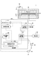
- FIG. 1 is a diagram illustrating an example of a plasma processing apparatus according to one embodiment.
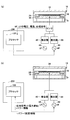
- FIG. 2 is a diagram illustrating an example of a configuration of a control unit according to one embodiment. The figure which shows the case where it controls by the phase signal of the sensor attached to the electric power feeding system which concerns on one Embodiment, or the case where it controls by the signal synchronized with the high frequency period of bias power.
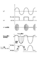
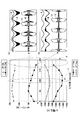
- FIG. 4 is a diagram illustrating an example of HF supply timing according to a phase within one cycle of LF according to an embodiment.
- FIG. 4 is a diagram illustrating an example of HF supply timing according to a phase within one cycle of LF according to an embodiment.
- FIG. 1 is a diagram illustrating an example of a plasma processing apparatus according to one embodiment.
- FIG. 2 is a diagram illustrating an example of a configuration of a control unit according to one embodiment. The figure which shows the case where it controls by the phase signal of the sensor attached to the electric power feeding system which concerns on one Embodiment, or
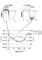
- FIG. 4 is a diagram illustrating an example of a relationship between a phase within one cycle of an LF, a plasma density Ne, and a self-bias Vdc according to an embodiment.
- FIG. 4 is a diagram showing an example of reflected wave power according to one embodiment.
- FIG. 4 is a diagram showing an example of reflected wave power according to one embodiment.
- FIG. 7 is a diagram for explaining a control method according to a first modification of the embodiment. The figure for explaining the control method concerning modification 2 of one embodiment. The figure for explaining the control method concerning modification 3 of one embodiment. The figure for explaining the control method concerning modification 4 of one embodiment.
- FIG. 2 is a diagram illustrating an example of an IMD (intermodulation distortion) according to an embodiment.
- IMD intermodulation distortion
- FIG. 9 is a timing chart showing a control method according to a modified example 5-1 of the embodiment.
- 13 is a timing chart showing a control method according to a modified example 5-2 of the embodiment.
- 13 is a timing chart showing a control method according to a modified example 5-3 of the embodiment.
- 13 is a timing chart showing a control method according to a modified example 5-4 of the embodiment.
- 13 is a timing chart illustrating a control method according to a modification 6 of the embodiment.
- 9 is a timing chart showing a control method according to a modified example 7-1 of the embodiment.
- 13 is a timing chart showing a control method according to a modified example 7-2 of the embodiment.
- 13 is a timing chart showing a control method according to a modified example 7-3 of the embodiment.
- FIG. 14 is a timing chart showing a control method according to a modified example 7-4 of the embodiment.
- FIG. 4 is a diagram illustrating an example of reflected wave power of source power according to one embodiment.
- 13 is a timing chart for explaining a control method according to Modification 8 of one embodiment.
- 21 is a timing chart for explaining a control method according to Modification 9 of the embodiment.
- 13 is a timing chart for explaining a control method according to Modification Example 10 of the embodiment.
- 13 is a timing chart for explaining a control method according to a modification 11 of the embodiment.
- 13 is a timing chart showing a control method according to Modification Example 12 of the embodiment.
- 14 is a timing chart showing a control method according to Modification 13 of one embodiment.
- the frequency (high frequency) of the source power is also referred to as “HF” (High Frequency), and the source power is also referred to as “HF power”.
- the frequency (high frequency) of the bias power having a frequency lower than the frequency of the source power is also referred to as “LF” (Low (Frequency), and the bias power is also referred to as “LF power”.
- IMD intermodulation distortion
- the IMD requires a high-frequency power source having a capacity capable of supplying a power larger than the originally required high-frequency power for not only causing a mismatch but also for the reflection resistance and maintaining the plasma. For this reason, conventionally, in order to reduce the occurrence of IMD, the cable length of a coaxial cable used for a power supply line of a high-frequency power supply has been optimized.
- the IMD occurs at the sum or difference frequency between the fundamental and / or harmonic of the HF power and the fundamental and / or harmonic of the LF power. For this reason, in the method of optimizing the cable length of the coaxial cable, although the reflected wave power of the high frequency power of a specific frequency can be reduced, the fundamental wave and / or harmonics of the HF power and the LF power included in the IMD can be reduced. It is not possible to eliminate reflected wave power at other frequencies resulting from the sum or difference with the wave.
- the IMD is generated at a frequency closer to the fundamental wave of the HF power. Therefore, the frequency of the LF power is increased as much as possible, and the occurrence of the IMD at a frequency closer to the fundamental wave of the HF power is suppressed. It is possible.
- the process result is better when the frequency of the LF power is lowered. That is, since the etching rate decreases as the hole with a high aspect ratio is etched deeper, the frequency of the LF power is made lower and the power is increased. This makes it possible to increase the etching rate in etching with a high aspect ratio.
- the reflected wave power of the high-frequency power has increased due to the recent increase in LF power and frequency.
- the reflected wave power of the high-frequency power increases.
- FIG. 12 shows an example of the reflected wave power generated when HF power of a predetermined frequency is applied to the electrode to which LF power is applied.
- the intensity of the IMD changes periodically in synchronization with the phase of Vpp (Peak to Peak) of the LF.
- Vpp Peak to Peak
- the IMD when the potential of the LF is near the positive maximum value, the IMD is almost 0 W, that is, there is no reflection. Further, the IMD is relatively low when the potential of LF is in the negative range. When the potential of the LF exceeds the positive maximum value and then multiplies by a negative value, the maximum reflected wave power is generated, and the IMD is maximized.
- the inventors propose a control method for suppressing the generation of the IMD according to the phase of the LF in consideration of the timing at which the IMD is generated, and a plasma processing apparatus that executes the control method. Furthermore, the present inventors propose a control method for controlling the amount and quality of radicals and ions by controlling high-frequency power of two different frequencies LF and HF.
- FIG. 1 is a diagram illustrating an example of a plasma processing apparatus according to one embodiment.
- the plasma processing apparatus 1 is a capacitively-coupled parallel plate plasma processing apparatus, and includes, for example, a cylindrical processing container 10 made of aluminum whose surface is anodized. The processing container 10 is grounded.
- a columnar support 14 is disposed on the bottom of the processing vessel 10 via an insulating plate 12 made of ceramics or the like, and a mounting table 16 made of, for example, aluminum is provided on the support 14.
- the mounting table 16 forms a lower electrode, on which a wafer W, which is an example of an object to be processed, is mounted via an electrostatic chuck 18.
- an electrostatic chuck 18 that suction-holds the wafer W with electrostatic force is provided.
- the electrostatic chuck 18 has a structure in which an electrode 20 made of a conductive film is sandwiched between a pair of insulating layers or insulating sheets.
- a DC power supply 22 is connected to the electrode 20.
- the DC voltage output from the DC power supply 22 is applied to the electrode 20.
- the wafer W is attracted and held on the electrostatic chuck 18 by electrostatic force such as Coulomb force generated thereby.
- a conductive edge ring 24 made of, for example, silicon is arranged on the mounting table 16 and around the wafer W.
- the edge ring 24 is also called a focus ring.
- a cylindrical inner wall member 26 made of, for example, quartz is provided on side surfaces of the mounting table 16 and the support table 14.
- a coolant chamber 28 is provided in the support base 14, for example, in an annular shape.
- a coolant at a predetermined temperature for example, cooling water is circulated and supplied from the chiller unit provided outside to the coolant chamber 28 through the pipes 30a and 30b, and the processing temperature of the wafer W on the mounting table 16 is controlled by the temperature of the coolant. Is done.
- the coolant is an example of a medium for temperature adjustment circulated and supplied to the pipes 30a and 30b, and the medium for temperature adjustment may not only cool the mounting table 16 and the wafer W but also heat it. .
- a heat transfer gas, for example, He gas, from the heat transfer gas supply mechanism is supplied between the upper surface of the electrostatic chuck 18 and the back surface of the wafer W via the gas supply line 32.
- an upper electrode 34 is provided in parallel so as to face the mounting table 16.
- a space between the upper electrode 34 and the lower electrode is a plasma processing space.
- the upper electrode 34 forms a surface that faces the wafer W on the mounting table 16 and is in contact with the plasma processing space, that is, forms an opposite surface.
- the upper electrode 34 is supported on the upper part of the processing container 10 via the insulating shielding member 42.
- the upper electrode 34 constitutes a surface facing the mounting table 16 and has an electrode plate 36 having a large number of gas discharge holes 37, and supports the electrode plate 36 in a detachable manner. And an electrode support 38 made of aluminum.
- the electrode plate 36 may be formed of, for example, silicon or SiC.
- a gas diffusion chamber 40 is provided inside the electrode support 38, and a large number of gas flow holes 41 communicating with the gas discharge holes 37 extend downward from the gas diffusion chamber 40.
- the electrode support 38 is provided with a gas inlet 62 for introducing a processing gas to the gas diffusion chamber 40, and a gas supply pipe 64 is connected to the gas inlet 62, and a processing gas supply source is connected to the gas supply pipe 64. 66 are connected.
- the gas supply pipe 64 is provided with a mass flow controller (MFC) 68 and an opening / closing valve 70 in order from the upstream side. Then, a processing gas for etching is supplied from the processing gas supply source 66.
- the processing gas reaches the gas diffusion chamber 40 from the gas supply pipe 64 and is discharged into the plasma processing space from the gas discharge hole 37 through the gas flow hole 41 in a shower shape. In this way, the upper electrode 34 functions as a shower head for supplying the processing gas.
- a variable DC power supply 50 is connected to the upper electrode 34, and a DC voltage from the variable DC power supply 50 is applied to the upper electrode 34.
- the control of the polarity and current / voltage of the variable DC power supply 50 and the electronic switch for turning on / off the current and voltage are controlled by the control unit 200.
- a first high frequency power supply 48 is connected to the mounting table 16 via a power supply rod 47 and a matching unit 46.
- the first high frequency power supply 48 applies LF power to the mounting table 16. Thereby, ions are drawn into the wafer W on the mounting table 16.
- the first high frequency power supply 48 outputs LF power having a frequency in the range of 200 kHz to 13.56 MHz.
- the matching unit 46 matches the internal impedance of the first high-frequency power supply 48 with the load impedance.
- a second high frequency power supply 90 is connected to the mounting table 16 via a power supply rod 89 and a matching unit 88.
- the second high frequency power supply 90 applies HF power to the mounting table 16.
- the frequency of the HF is higher than the frequency of the LF, and HF power of a frequency of 13.56 MHz or more is output from the second high frequency power supply 90.
- HF power for example, for LF power of 400 kHz, HF power of 100 MHz having a higher frequency may be output.
- the matching unit 88 matches the internal impedance of the second high-frequency power supply 90 with the load impedance.
- a filter 94 for passing a predetermined high frequency to the ground may be connected to the mounting table 16. The HF power supplied from the second high frequency power supply 90 may be applied to the upper electrode 34.
- An exhaust port 80 is provided at the bottom of the processing container 10, and an exhaust device 84 is connected to the exhaust port 80 via an exhaust pipe 82.
- the exhaust device 84 has a vacuum pump such as a turbo molecular pump, and can reduce the pressure inside the processing container 10 to a desired degree of vacuum.
- a loading / unloading port 85 for the wafer W is provided on a side wall of the processing container 10, and the loading / unloading port 85 can be opened and closed by a gate valve 86.
- a deposition shield 11 for preventing the etching by-product (depot) from adhering to the processing container 10 along the inner wall of the processing container 10 is detachably provided. That is, the deposition shield 11 constitutes the wall of the processing container.
- the deposit shield 11 is also provided on the outer periphery of the inner wall member 26.
- An exhaust plate 83 is provided between the deposition shield 11 on the processing container wall at the bottom of the processing container 10 and the deposition shield 11 on the inner wall member 26 side.
- an aluminum material coated with ceramics such as Y 2 O 3 can be used as the deposit shield 11 and the exhaust plate 83.
- the gate valve 86 is opened, and the wafer W to be etched is loaded into the processing chamber 10 through the loading / unloading port 85, and the mounting table is set. 16 is placed. Then, a processing gas for etching is supplied from the processing gas supply source 66 to the gas diffusion chamber 40 at a predetermined flow rate, and is supplied into the processing container 10 through the gas flow holes 41 and the gas discharge holes 37. Further, the inside of the processing container 10 is exhausted by the exhaust device 84, and the pressure therein is set to a set value within a range of, for example, 0.1 to 150 Pa.
- processing gas various kinds of conventionally used gases can be adopted, and for example, a gas containing a halogen element such as a C 4 F 8 gas can be suitably used. Further, another gas such as an Ar gas or an O 2 gas may be contained.
- HF power is applied to the mounting table 16 from the second high frequency power supply 90.
- LF power is applied to the mounting table 16 from the first high frequency power supply 48.
- a DC voltage is applied to the upper electrode 34 from the variable DC power supply 50.
- a DC voltage is applied from the DC power supply 22 to the electrode 20 to attract and hold the wafer W on the mounting table 16.
- the processing gas discharged from the gas discharge holes 37 of the upper electrode 34 is dissociated and ionized mainly by HF electric power to generate plasma.
- the processing surface of the wafer W is etched by radicals and ions in the plasma. Further, by applying LF power to the mounting table 16, ions in the plasma are controlled, and etching of holes with a high aspect ratio can be performed, and the plasma control margin can be widened.
- the plasma processing apparatus 1 is provided with a control unit 200 for controlling the operation of the entire apparatus.
- the control unit 200 executes desired plasma processing such as etching in accordance with a recipe stored in a memory such as a ROM (Read Only Memory) and a RAM (Random Access Memory).
- the recipe includes process time, pressure (gas exhaust), high-frequency power and voltage, various gas flow rates, processing chamber temperature (upper electrode temperature, processing chamber side wall temperature, wafer W temperature) which are control information of the apparatus with respect to the process conditions. , The temperature of the electrostatic chuck, etc.), the temperature of the refrigerant output from the chiller, and the like.
- these programs and recipes indicating processing conditions may be stored in a hard disk or a semiconductor memory.
- the recipe may be set at a predetermined position and read out in a state of being stored in a portable computer-readable storage medium such as a CD-ROM or a DVD.
- the HF power on / off or High / Low is converted to a signal synchronized with the high frequency cycle of the bias power, or to the phase within one cycle of any one of the voltage, current or electromagnetic field measured by the power supply system of the bias power.
- You may control so that it may be synchronized.
- the control unit 200 may perform control so as to synchronize on / off of the power of the HF or High / Low with a phase within one cycle of the voltage or the current of the LF. Thereby, the quantity and quality of ions and radicals can be controlled. Further, occurrence of IMD can be reduced.
- the power supply system of the bias power means the first high-frequency power supply 48 ⁇ matching unit 46 ⁇ power supply rod 47 ⁇ mounting table 16 ⁇ (plasma) ⁇ upper electrode 34 ⁇ (ground).
- the voltage, current, or electromagnetic field measured in the power supply system of the bias power refers to parts from the first high-frequency power supply 48 to the inside of the matching box 46 and to the mounting table 16 via the power supply rod 47 and the upper electrode. Refers to the voltage, current or electromagnetic field measured at.
- the state of a signal synchronized with the high-frequency cycle of the bias power, or any of the voltage, current, or electromagnetic field measured by the bias power supply system is also referred to as a “reference electric state”.
- the HF power source power
- the HF power is controlled so as to be alternately applied to a first state and a second state described later in synchronization with a phase within one cycle of the reference electric state.
- the reference electric state is determined by the matching device connected from the mounting table 16 via the power supply rod 47. Is preferably one of a voltage, a current, and an electromagnetic field measured in any member up to the inside.
- a voltage probe, a current probe, and a BZ probe are installed near any part of the power supply system of the bias power.
- a method of measuring the voltage, current or induced magnetic field of a part is a method of measuring the voltage, current or induced magnetic field of a part.
- FIG. 2B (a) is an example of a case where any of the voltage, current, or electromagnetic field measured in the bias power supply system is set to the “reference electric state”.
- the processor 100 inputs any of the HF voltage or current, the LF voltage or current, the HF phase signal, or the LF phase signal from a sensor such as a VI probe attached to the power supply system. .
- the processor 100 sets the source power to the first in synchronization with the phase in one cycle of the reference electrical state indicating either the input HF voltage or current, the LF voltage or current, the HF phase signal, or the LF phase signal. And the second state are applied alternately.
- the processor 100 may generate a signal synchronized with the high-frequency cycle of the bias power output from the first high-frequency power supply 48 without being based on the signal from the sensor.
- the state of the signal can be set as the reference electric state.
- the step of measuring the reference electric state in the power supply system of the bias power can be omitted.
- the processor 100 inputs an LF phase signal (small power waveform) or a signal related to bias power information from the first high frequency power supply 48, and based on the input signal, a high frequency cycle of the bias power.
- Generate a signal synchronized with The processor 100 outputs the generated signal to the second high frequency power supply 90.
- the second high frequency power supply 90 alternately applies the source power to the first state and the second state based on this signal.
- the processor 100 may generate a signal synchronized with the high-frequency cycle of the bias power without using the signal from the first high-frequency power supply 48.
- the processor 100 generates, for example, a signal having a period indicated by LF in FIG. 3, and generates an on / off signal indicated by HF in FIG. 3, for example, in synchronization with the signal.
- the processor 100 outputs the generated signal to the first high-frequency power supply 48 and the second high-frequency power supply 90.
- the first high frequency power supply 48 outputs bias power based on this signal.
- the second high frequency power supply 90 alternately applies the source power to the first state and the second state based on this signal.
- the mounting table 16 is an example of a first electrode on which the wafer W is mounted.
- the upper electrode is an example of a second electrode facing the first electrode.
- the first high-frequency power supply 48 is an example of a bias power supply that supplies LF power to the first electrode.
- the second high-frequency power supply 90 is an example of a source power supply that supplies HF power having a frequency higher than LF power to the first electrode or the second electrode.
- the control unit 200 is an example of a control unit that controls a bias power supply and a source power supply.
- the potential of the lower electrode (mounting table 16) to which the bias power is applied is also referred to as an electrode potential.
- the control unit 200 includes a processor 100, a signal generation circuit 102, directional couplers 105 and 108, a reflection detector 111, and an oscilloscope 112.
- a directional coupler 105 is connected between the first high-frequency power supply 48 and the matching unit 46 to the power supply line of the first high-frequency power supply 48.
- a directional coupler 108 is connected between the second high-frequency power supply 90 and the matching unit 88 to the power supply line of the second high-frequency power supply 90.
- the directional coupler 105 gives a part of the traveling wave power (Pf) of the LF to the oscilloscope 112. Further, the directional coupler 108 supplies a part of the traveling wave power and the reflected wave power of the HF to the oscilloscope 112.
- the LF frequency displayed on the oscilloscope 112 is, for example, 400 kHz, and the HF frequency is, for example, 100 MHz.
- the oscilloscope 112 can observe the waveform of the LF traveling wave power, the waveform of the HF traveling wave power, and the waveform of the HF reflected wave power.
- the directional coupler 108 separates a certain percentage of the HF reflected wave and supplies the same to the reflection detector 111.
- the reflection detector 111 is composed of, for example, a spectrum analyzer, a power meter, and the like, and measures how much IMD (Intermodulation distortion) of what wavelength is generated and how much reflected wave power is.
- the IMD applies a LF power to the upper electrode or the lower electrode of the plasma processing apparatus 1 (a lower electrode in one embodiment), and applies an LF power to the lower electrode to generate a fundamental wave and / or a harmonic of the LF.
- the power of the reflected wave from the plasma side generated according to the frequency of the sum or difference with the fundamental wave and / or the harmonic of HF.
- the -directional coupler 105 provides a part of the LF traveling wave power to the processor 100.
- the processor 100 creates a synchronization signal for HF synchronized with the traveling wave power of LF.
- the processor 100 may create a synchronization signal for HF in synchronization with the positive timing of the traveling wave of LF.
- an LF waveform detected using a sensor such as a VI probe may be provided to the processor 100.
- the processor 100 gives the created synchronization signal to the signal generation circuit 102.
- the signal generation circuit 102 generates a control signal synchronized with the LF traveling wave power from the applied synchronization signal, and supplies the control signal to the second high-frequency power supply 90 and the first high-frequency power supply 48.
- the directional coupler 105 extracts a part of the LF voltage or current output from the first high-frequency power supply 48 as a waveform and inputs the waveform to the processor 100.
- the processor 100 may directly input a part of the power of the LF or the like from the first high-frequency power supply 48.
- the processor 100 generates an ON signal having an arbitrary delay and an arbitrary width from the input waveform signal, and transmits the ON signal to the signal generation circuit 102.
- the ON signal is an example of a synchronization signal.
- the signal generation circuit 102 sends a command signal to the second high-frequency power supply 90 to generate HF power during the ON signal.
- a command signal a control signal for generating HF power or the ON signal itself during the ON signal is used depending on the input form of the second high-frequency power supply 90.
- the signal from the directional coupler 105 is not used, and the signal generation circuit 102 outputs the LF output from the first high frequency power supply 48. May be extracted as a waveform, and an ON signal having an arbitrary delay and an arbitrary width may be created from the waveform signal.
- the signal generation circuit 102 transmits the waveform signal and the ON signal to the second high frequency power supply 90.
- the method of generating the control signal described above is an example, and the present invention is not limited to this.
- the HF power is turned on / off or High / Low alternately in synchronization with the phase within one cycle of the reference electric state (the phase within one cycle of the LF voltage or current, the electrode potential, etc.).
- the circuit is not limited to the circuit of the control unit 200 shown in FIG. 2A, and other hardware or software can be used.
- the amplifier of the first high-frequency power supply 48 amplifies the amplitude (AM: amplitude modulation) of the LF modulation signal of 400 kHz and supplies it to the lower electrode.
- the amplifier of the second high-frequency power supply 90 amplifies the amplitude of the HF modulation signal of 100 MHz and supplies it to the lower electrode.
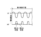
- FIG. 3 is a diagram showing an example of a waveform of an LF voltage or current and an example of an HF voltage or current applied in accordance with a positive timing of the LF voltage or current.
- the electrode potential shown in the second waveform from the bottom is positive, the voltage or current of HF is controlled (turned on) to a positive value.
- the electrode potential is negative, the voltage or current of HF is controlled (turned off) to zero.
- the electrode potential is determined by the voltage or current of LF, the voltage or current of HF is turned off when the voltage or current of LF is negative, and the voltage or current of HF is turned off when the voltage or current of LF is positive. The current is turned on.
- the processor 100 may generate the synchronization signal for controlling the power of the HF during a time period including the timing when the electrode potential is positive.
- the processor 100 is not limited to this, and may generate the synchronization signal for controlling the power of the HF in a short time including the timing when the electrode potential becomes the deepest negative.
- FIG. 4 is a diagram illustrating an example of a supply timing of HF power according to the embodiment.
- the vertical axes in FIGS. 4A to 4C indicate the potentials of the electrodes.
- the potential of the electrode is almost the same as the potential of the wafer.
- the electrode potential is the potential when the LF and HF voltages are superimposed.
- Vpp of the LF voltage having the LF frequency of 400 kHz is much larger than Vpp of the HF voltage having the HF frequency of 100 MHz. Therefore, basically, the electrode potential is determined by the voltage of LF, and the electrode oscillates within the width (amplitude) of Vpp of the voltage of HF.
- the thickness of the sheath on the electrode is basically determined according to the voltage of the LF.
- the electrode potential when the LF voltage is negative becomes deeper than the electrode potential when the LF voltage is positive due to the so-called self-bias voltage Vdc.
- Vdc self-bias voltage
- the electrode Since the electrode is floating from the ground by a blocking capacitor (a matching device in one embodiment), electrons flowing into the electrode do not flow to the ground. Therefore, electrons flow into the electrode and accumulate at a period (half cycle) in which the surface of the electrode is at a positive potential with respect to the plasma. However, the surface of the electrode is negatively charged due to the accumulated electrons, and a negative bias is generated with respect to the plasma. The negative bias causes ions to flow into the surface of the electrode. Thereby, a sheath is formed on the surface of the electrode.
- FIG. 3 schematically shows the electrode potential corresponding to the phase of LF, the plasma potential corresponding to the phase of LF, the sheath thickness, and the impedance Z.
- the plasma potential is slightly higher than the highest potential in the processing chamber 10. Therefore, the plasma potential is slightly higher than the electrode potential when the electrode potential is positive, and slightly higher than the potential 0 on the wall when the potential of the wall of the processing vessel 10 is 0 when the electrode potential is negative.
- the thickness of the sheath is proportional to the voltage. Therefore, when the electrode potential is negative, a large voltage is applied to the electrode, and the thickness of the sheath decreases. It gets thicker. On the other hand, when the electrode potential is positive, a smaller voltage is applied to the electrode than when the electrode potential is negative, so that the thickness of the sheath is reduced.
- the electrode potential shown in FIG. 4 is the lower electrode potential.
- the impedance Z is high and the change is large because the sheath is thick. Further, the impedance Z is substantially determined by the voltage of LF. As described above, impedance matching of HF power becomes difficult. In particular, when the electrode potential is negative, that is, when the voltage of the LF is negative, the impedance is high and the change is large, so that the impedance matching of the HF power becomes difficult.
- the matching device 88 that performs impedance matching with respect to the HF power with respect to such a variation in the impedance Z can follow up to a frequency of about 1 Hz at maximum by operating the motor. This makes it difficult to match the timing of one of the impedances that change momentarily according to the phase of the LF. In this state, since the matching unit 88 cannot match at a phase other than the matched one timing, the reflected wave power of the IMD is large.
- the power of the HF is controlled to be ON or High when the electrode potential is positive, and the HF power is controlled when the electrode potential is negative.
- the power is controlled to be off or low.
- the impedance Z is substantially constant, so that if HF power is supplied at this timing, matching can be easily achieved. Therefore, at this timing, the HF power is controlled to be ON or High.
- the electrode potential is negative, the impedance is high and the change is large, so that it is difficult to achieve matching even when HF power is supplied at this timing. Therefore, at this timing, the supply of the HF power is controlled to be off or low. Thereby, the occurrence of IMD can be reduced.
- the power of the HF when the power of the HF is controlled to be high or low, the power of the HF is turned on or off because the power of the HF is kept low without turning off the power of the HF when the electrode potential is negative.
- the decrease in plasma density can be suppressed as compared with the case of controlling.
- the power of HF applied at the timing when the electrode potential is negative smaller than the power of HF applied at the timing when the electrode potential is positive, the occurrence of IMD can be suppressed.
- the control method for turning on or high the power of the HF by making the electrode potential coincide with the positive timing is an example, and is not limited to this.
- the power of the HF may be controlled to be ON or High.
- the power of the HF may be controlled to be ON or High. That is, the HF power (source power) has a first state and a second state smaller than the first state, and the period of the first state includes a timing at which the phase of the reference electric state becomes a peak. You may go out.
- the peak in this case may be a positive peak or a negative peak.
- At least a part of the phase of the reference electric state may include a positive timing. Further, the period of the first state may include at least a part of the phase of the reference electric state including a negative timing.
- the power of the HF is not limited to a rectangular wave whose phase in the reference electric state is coincident with the positive timing, but also applies a substantially rectangular wave including at least one of a rising slow-down and a falling slow-down. Good. Further, the power of the HF may be applied to at least one of a timing at which the phase of the reference electrical state is shifted by a predetermined time from the positive timing or a timing shifted by a predetermined time.
- An example of the use of the control method for shifting the power of the HF by a predetermined time from the timing when the phase of the reference electric state is positive is as follows. If the power of HF is applied only when the phase of the reference electric state is positive, the ion energy decreases. Depending on the type of etching, a process with a higher ion energy may be desired. In that case, the power of the HF is applied until the reference electric state of the LF changes from positive to negative and ion energy of a desired magnitude is obtained. Thereby, a process with a large ion energy can be realized.
- the time width for supplying the power of the HF may be adjusted such that the power of the HF is shortened or lengthened by a predetermined time based on the timing when the phase of the reference electric state is positive.
- the power of the HF may be supplied by adding a predetermined time before and after the timing when the phase of the reference electric state is positive.
- the power of the HF may be supplied at the timing when the phase of the reference electric state is negative.
- the phase of the reference electric state is negative, the impedance is high and changes with time. Therefore, in this case, it is preferable to control the HF power to be turned on for a shorter time width when the phase of the reference electric state is negative.
- the power of the HF when the electrode potential is negative, the power of the HF is turned on or high for a short time width including the time when the self-bias Vdc of the electrode is most negative, and the other times.
- the power of the HF may be turned off or low.
- the reflected wave power is detected in advance, and the power of the HF is turned off or low during a time period where the reflected wave power is high, and the power of the HF is turned on or off during a time period where the reflected wave power is low, depending on the magnitude of the reflected wave power. It may be High.
- HARC High Aspect Ratio Ratio Contact
- the power of the HF is turned on / off or the High / Low is controlled in synchronization with the phase in one cycle of the reference electric state. .
- the occurrence of IMD can be reduced.
- the state in which the power of the HF is controlled to be ON or High is an example of the first state.
- the state in which is controlled to OFF or Low is an example of the second state.
- the control method of the plasma processing apparatus 1 includes a first control step of alternately applying the first state and the second state in synchronization with a phase within one cycle of the reference electric state.
- the second state only needs to be smaller than the first state, and the power in the second state may be 0 or may be a value other than 0 smaller than the first state.
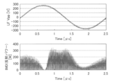
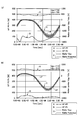
- the graph of FIG. 5 is a diagram illustrating an example of the relationship between the phase of the LF, the plasma density Ne, and the absolute value
- 6 and 7 are diagrams illustrating an example of the reflected wave power according to the embodiment.
- the graph of FIG. 5 is an actual measurement result obtained by periodically applying the power of the HF with a time width of about 40% of the one cycle while changing the phase with respect to one cycle of the reference electric state, and measuring.
- the vertical axis shows the plasma density Ne (cm ⁇ 3 ), and the right vertical axis shows the absolute value
- the sheath of the lower electrode fluctuates in the cycle of LF, and as a result, the impedance Z changes to change the plasma density Ne and the self density.
- the bias Vdc fluctuates.
- the plasma density Ne becomes medium to high, and the plasma generation efficiency becomes medium or higher. This is because when the electrode potential is negative, a large voltage is applied to the electrode, the thickness of the sheath increases, the HF electric field when the HF power is turned on decreases, and the plasma generation efficiency decreases.
- of the self-bias is high, and the ion energy can be made monochromatic, that is, ions having the same ion energy can be drawn into the wafer W.
- monoenergized high-energy ions can be drawn into the wafer W.
- the occurrence of IMD increases, but by applying HF power in a short time when the potential of the lower electrode becomes the largest negatively, the total occurrence of IMD is reduced as compared with the case where HF power is constantly applied. it can.
- the plasma processing apparatus 1 for example, by controlling the power of the HF to be on or high based on the timing when the electrode potential is positive, the occurrence of IMD can be reduced.
- the problem is that the plasma generation efficiency is reduced by increasing the thickness of the sheath when the electrode potential is negative, and the plasma generation efficiency is increased by applying HF power at the positive electrode potential timing. it can.
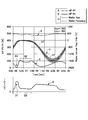
- the upper and lower graphs on the left in FIG. 6 and the waveforms on the screens in (a) and (b) on the right in FIG. 6 show an example of the detection result by the reflection detector 111 of the control unit 200 and the display result of the oscilloscope 112. .
- the lower left graph shows Vpp and Vdc in one cycle of LF. The sheath becomes thicker as Vdc becomes deeper negatively, and the plasma generation efficiency when HF power is applied decreases.
- the upper graph shows the traveling wave power (Pf) and the reflected wave power (Pr) of HF with respect to Vpp and Vdc in one cycle of LF.
- An example of the display of the oscilloscope 112 in FIG. 6A is a waveform A of the traveling wave power of the LF measured when the phase of the LF shown in the region c is 180 °, and an amplitude B of the high-frequency power on the wafer (that is, the amplitude B). , LF power and HF power).
- the waveform of the traveling wave power of HF is indicated by C
- the waveform of the reflected wave power of HF is indicated by D.
- the amplitude B of the high-frequency power, the waveform C of the traveling wave power of HF, and the waveform D of the reflected wave power of HF are shown.
- the reflected wave power is smaller in the region d than in the region c. Therefore, a signal synchronized with the high frequency cycle of the bias power so that the phase of the LF includes 0 ° or a phase within one cycle of the reference electric state measured by the power supply system of the bias power is synchronized with the power of the HF.
- a first state for example, ON or High state
- a second state for example, OFF or Low state
- of the plasma, and IMD can be suppressed and plasma generation efficiency can be increased.
- the power of the HF between the first state and the second state at an arbitrary timing according to the electrode potential a region where the plasma density Ne is high and a region where the absolute value
- the generation of IMD can be reduced as a whole by applying the HF power in a pulse shape.
- FIG. 7 shows an example of LF ⁇ Vpp, LF ⁇
- the reflected wave power (Pr) of the HF changes by a maximum of about 5 times (about 10 W to about 50 W) in the phase of one cycle of the voltage of the LF.
- the IMD can be reduced to about 1/5 by controlling the power of the HF in synchronization with the phase in one cycle of the reference electric state.
- the maximum value is about 1.6 times the minimum value. It can be seen that it can be changed.
- FIG. 8 is a diagram illustrating a control method according to a first modification of the embodiment.
- FIG. 9 is a diagram for describing a control method according to Modification 2 of the embodiment.
- FIG. 10 is a diagram for describing a control method according to Modification 3 of one embodiment.
- FIG. 11 is a diagram illustrating a control method according to Modification 4 of the embodiment.
- Modification 1 In the embodiment described above, when the HF power is pulse-modulated (refer to HFAM modulation in FIG. 3) in synchronization with the phase in one cycle of the reference electric state, the pulse modulation is performed at the same frequency as the LF frequency. An HF power supply is required, which may increase costs.
- a bypass line is provided for a power supply line or a lower electrode connected to the first high-frequency power supply 48 and the second high-frequency power supply 90.
- the constituent additional circuit 250 is attached.
- a coil 252 and a variable capacitor 251 are connected in series to a power supply rod connected to a lower electrode, and the variable capacitor 251 is connected to the processing container 10 and grounded.
- the additional circuit 250 By making the ratio of the impedance on the processing vessel 10 side to the load impedance on the plasma side larger by the additional circuit 250, even if the impedance changes compared to the case without the additional circuit 250, the additional circuit 250 A large change in the impedance Z, which is the sum of the impedances on the container 10 side, can be mitigated.
- the additional circuit 250 reduces the change in the total impedance Z so that the HF power is applied in synchronization with the phase in one cycle of the reference electric state. , IMD can be further suppressed. Further, a mechanism for suppressing the IMD can be simply and inexpensively constructed simply by attaching the additional circuit 250.
- the additional circuit 250 is preferably inserted into the second high-frequency power supply 90 after the branch of the power supply rod, because the HF power is less likely to be affected by the LF power. If a filter is provided between the first high-frequency power supply 48 and the second high-frequency power supply 90, the HF power is less likely to be affected by the LF power, the fluctuation of the total impedance Z can be reduced, and the occurrence of IMD can be reduced. Can be suppressed.
- the additional circuit 250 may include at least one of a coil, a capacitor, and a diode.
- the plasma processing apparatus 1 includes an impedance change circuit 300 connected to a power supply line or a lower electrode connected to the first high-frequency power supply 48 and the second high-frequency power supply 90. Is attached.
- the impedance changing circuit 300 functions to change the impedance such that the combined impedance of the load impedance on the plasma side and the impedance of the impedance changing circuit 300 becomes constant.
- the impedance changing circuit 300 changes the impedance according to the phase of the LF so as to suppress the change in the impedance viewed from the matching unit 88. Thereby, the reflected wave power can be suppressed, and the occurrence of IMD can be reduced.
- the impedance changing circuit 300 changes the impedance within one cycle of the reference electrical state according to the phase (or impedance) of the LF, the Vdc of the LF, the reflected wave power, and the like, thereby suppressing the IMD.
- the impedance change circuit 300 As an example of the impedance change circuit 300, a configuration in which capacitors are provided in an array and the connection of the capacitors is switched by an electronic switch can be given.
- the control unit 200 controls the electronic switch to change the impedance of the impedance changing circuit 300.
- the control unit 200 connects the capacitors of the impedance changing circuit 300 so as to reduce the change in the impedance Z that is the sum of the load impedance on the plasma side and the impedance of the impedance changing circuit 300. Switch. Thereby, when the power of the HF is applied in synchronization with the phase in one cycle of the reference electric state, the impedance matching becomes good, and the occurrence of IMD can be further suppressed.
- the impedance change circuit 300 may be inserted into the matching unit 88 and integrated with the matching unit 88.
- the impedance change circuit 300 is preferably inserted into the second high-frequency power supply 90 after the branch of the power supply rod because the HF power is less likely to be affected by the LF power. If a filter is provided between the first high-frequency power supply 48 and the second high-frequency power supply 90, the HF power is less likely to be affected by the LF power, the fluctuation of the total impedance Z can be reduced, and the generation of IMD can be reduced. Can be suppressed.
- an electromagnet 350 is provided at an upper portion of the processing container 10.
- the position of the electromagnet 350 is not limited to the position shown in FIG. 10A, and may be any part of the processing container 10, for example, inside the processing container 10.
- the control unit 200 controls the strength of the electromagnet 350 according to the phase (or impedance) of the reference electric state, the phase of the LF, the electrode potential to which the bias power is applied, the reflected wave power of the LF Vdc or the HF, etc. Change the characteristics of For example, as shown in FIG.
- the electromagnet 350 can be a multipole electromagnet or a fixed magnet, and is an example of a magnetic field generating unit that generates a magnetic field.
- the control by the electromagnet 350 shown in Modification 3 may be used together with the control by the additional circuit 250 of Modification 1 or the impedance change circuit 300 of Modification 2.
- the matching unit 88 functions to add all the L and C components of the inductance (for example, a power supply rod) and the conductance (for example, a sheath) in the processing container 10 and function to resonate at the frequency of HF. I take the.
- the matching unit 88 since the C component changes when the sheath thickness changes, the power of the reflected wave increases if the matching device 88 does not match again in response to the change in the C component due to the change in the sheath thickness. .
- the matching unit 88 takes about one second to move the variable capacitor, it may not be able to follow a change in the thickness of the sheath, and may not be able to achieve accurate matching.
- the control unit 200 changes the frequency of the HF by the change of the C component due to the change of the sheath thickness. That is, based on the expression of the supply frequency of f (supply frequency) ⁇ 1 / ⁇ LC, the frequency f of the HF is changed according to the change of the C component corresponding to the thickness of the sheath.
- the capacitance of the sheath on the electrode is C
- the capacitance C changes four times according to the change in the thickness of the sheath
- the frequency of the HF changes approximately two times.
- the frequency of the HF changes about 3.3 times.
- the HF frequency is set in the above-described equation of the resonance frequency so as to match the change in the sheath thickness in accordance with the change in the LF voltage in one cycle. Change based on As a result, the matching is substantially achieved in accordance with the change in the thickness of the sheath, the reflected wave power of the HF can be reduced, and the occurrence of IMD can be suppressed.
- the second high-frequency power supply 90 uses a variable frequency power supply capable of changing the frequency of HF.
- the control shown in Modification 4 may be used in combination with at least one of the additional circuit 250 of Modification 1, the impedance changing circuit 300 of Modification 2, or the electromagnet 350 of Modification 3.
- the shift time and the delay width may be adjusted by a circuit having a gate function and a delay function based on the original signal and the measurement signal.
- LF pulse instead of controlling the timing of applying the power of the HF in synchronization with the phase within one cycle of the voltage of the LF, as shown in FIG. , "LF pulse"
- the timing of applying the HF power may be controlled in accordance with the LF pulse. That is, for example, the LF pulse corresponding to the LF of 400 kHz may be turned on / off and applied, and the power of the HF may be controlled in a pulse form (HF pulse) accordingly.
- the power of the LF pulse corresponding to the peak of the phase of the reference electric state may be applied, and the timing of applying the power of the HF may be controlled according to the LF pulse.
- the intensity of generation of the IMD varies depending on the power of the LF.
- the IMD is selected by selecting the timing at which the HF reflected wave power is low and applying the HF power at that timing. Can be reduced.
- the stability of the process and the plasma processing apparatus 1 can be improved, and the apparatus cost can be reduced.
- the LF power and the HF power may be applied at each of the two timings including the time when the reference electric state peaks twice in one cycle.
- the control method of the application of the HF power can be freely changed.
- the application of the HF power is not limited to the lower electrode, and may be applied to the upper electrode.
- the bias power is supplied to the lower electrode on which the wafer W is mounted, and the frequency higher than the bias power is supplied to the lower electrode.
- the source power has a first state and a second state, and a signal that synchronizes the first state and the second state with a high-frequency cycle of the bias power, or power supply of the bias power.
- a method of controlling a plasma processing apparatus other than the parallel plate type plasma processing apparatus includes a step of supplying bias power to the lower electrode and a step of supplying source power having a frequency higher than the bias power to the plasma processing space. Also in the control method, the source power has a first state and a second state, and the first state and the second state are alternately synchronized with a phase in one cycle of the reference electric state. The method includes a first control step of applying.
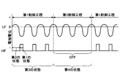
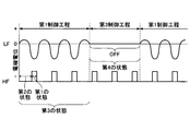
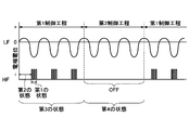
- Modifications 5-1 to 5-4 Next, a control method of the plasma processing apparatus 1 according to Modifications 5-1 to 5-4 of the embodiment will be described. In the modified examples 5-1 to 5-4, control for intermittently stopping the source power and / or the bias power is performed. 13A to 13D are timing charts showing control methods according to Modifications 5-1 to 5-4 of the embodiment.
- Modification 5-1 in FIG. 13A includes, in addition to the first control step, a second control step in which the source power is intermittently stopped by the LF voltage at a period independent of the period of the reference electric state, which is an example.
- the first control step and the second control step are repeatedly executed.
- the LF voltage is applied in the same cycle in the first control step and the second control step.
- the source power alternately repeats the first state and the second state at least once in the first control step, and is intermittently stopped in the second control step between the first control steps.
- the frequency of the LF may be, for example, 0.1 Hz to 100 Hz.
- the state of the source power synchronized with the cycle of the reference electric state in the first control step is an example of the third state.
- the state of the source power independent of the cycle of the reference electric state in the second control step is an example of a fourth state different from the third state.
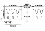
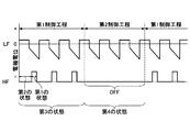
- the control method according to the modified example 5-2 in FIG. 13B includes the same first control step as the modified example 5-1 and additionally intermittently stops the bias power at a period independent of the period of the HF voltage or current.
- a third control step is included.
- the state of the bias power in the third control step is an example of the fourth state.
- the first control step and the third control step are repeatedly executed.
- the source power in the third control step is such that the first state and the second state are repeated in the same cycle as in the first control step.
- the frequency of the LF may be, for example, 0.1 Hz to 100 Hz.
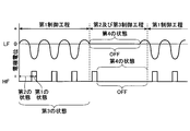
- the control method according to Modification 5-3 of FIG. 13C includes the same first control step as Modification 5-1 as well as the control of the source power in the second control step of Modification 5-1 and Modification 5-2 Is performed in the third control step. That is, the state in which both the source power and the bias power are intermittently stopped in the modified example 5-3 is an example of the fourth state.
- the cycle in which the bias power is intermittently stopped and the cycle in which the source power is intermittently stopped may be synchronized.
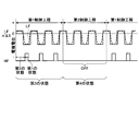
- the period in which the source power and the bias power are intermittently stopped may be the same as shown in FIG. 13C, or the source power and the bias power may be shifted behind the bias power as shown in FIG. 13D.
- the source power may be shifted before the bias power.
- the stop time of the source power may be longer or shorter than the stop time of the bias power.
- the control methods according to Modifications 5-1 to 5-4 can control the quality and quantity of radicals and ions. Specifically, when the HF is turned off, the ions in the plasma almost disappear, but the radicals have a long life and exist without disappearing for some time. Therefore, for example, while turning off the HF, the radicals can be diffused uniformly. In addition, while the HF is controlled to be off or low, the ratio of ions to radicals in the plasma can be changed. Thereby, the amounts of radicals and ions can be controlled.
- radicals corresponding to the progress of the dissociation are generated.
- the dissociation of C 4 F 8 gas proceeds as C 4 F 8 ⁇ C 4 F 7 * ⁇ ... ⁇ CF 2, and different radicals (such as C 4 F 7 * ) are generated depending on the degree of dissociation. Is done.
- the parameters that cause dissociation include ion energy and reaction time. Therefore, the ion energy and / or reaction time can be controlled by controlling the application timing and application time of the bias power and the source power, and the quality of radicals and ions can be controlled by promoting the generation of radicals suitable for the process.
- the bias power is off
- the ion energy decreases, so that the etching does not proceed, and the by-products deposited at the bottom of the holes and the like can be removed outside the holes and deposited on the mask.
- radicals can be attached to the pattern surface on the wafer W.
- the radicals attached to the mask protect the mask and improve the mask selectivity. Thereby, etching can be promoted, the etching rate can be increased, and the etching shape can be improved.
- plasma may be generated by the bias power, and the same effect may be obtained when the bias power is intermittently stopped. That is, by intermittently stopping the bias power, the quality and quantity of radicals and ions can be controlled. Thereby, the etching rate can be increased and the etching shape can be improved.
- the source power in the third state, is turned on at a timing when LF @ Vdc is deeply negative.
- the source power may be turned on.
- the source power instead of periodically turning on / off the source power, the source power may be periodically controlled to High / Low.
- FIG. 14 is a timing chart illustrating a control method according to Modification 6 of the embodiment.
- an LF pulse is applied to the mounting table 16 as shown in FIG.
- the positive value of the LF pulse corresponds to the positive peak of the LF voltage
- the negative value of the LF pulse corresponds to the negative peak of the LF voltage.
- the first state and the second state of the HF are alternately applied in synchronization with the phase within one cycle of the LF pulse. This can also control the quantity and quality of radicals and ions.
- the source power is controlled to be off or low during part or all of the period when the LF pulse is positive, and the source power is controlled to be on or high during part or all of the period when the LF pulse is negative. Good. According to this, since the LF pulse is binarized and the source power is binarized and controlled in accordance with the binarization, the control becomes easy.
- the state of the HF shown in FIG. 13A is controlled in accordance with the LF pulse obtained by pulsing the LF voltage in FIG. 13A, but the invention is not limited to this.
- the state of the HF shown in FIGS. 13B to 13D may be controlled in accordance with the LF pulse obtained by pulsing the LF voltage in FIGS. 13B to 13D.
- FIG. 15A is a timing chart illustrating a control method according to Modification 7-1 of the embodiment.
- FIG. 15B is a timing chart illustrating a control method according to Modification 7-2 of one embodiment.
- FIG. 15C is a timing chart illustrating a control method according to Modification 7-3 of one embodiment.
- FIG. 15D is a timing chart illustrating a control method according to Modification 7-4 of the embodiment.
- the first state and the second state of the source power are set to the LF voltage and the electrode potential. Are alternately applied in synchronization with the phase within one cycle of the reference electric state.
- the first state of the source power has two or more states stepwise in synchronization with the negative timing of the electrode potential.
- the first state of the source power has two or more states smoothly in synchronization with the negative timing of the electrode potential.
- the first state of the source power may be synchronized with the positive timing of the electrode potential.
- the control methods according to the modified examples 7-3 and 7-4 shown in FIGS. 15C and 15D include a second control step in addition to the first control step, and in the first control step, the source power is reduced.
- the first state and the second state are alternately applied in synchronization with the phase within one cycle of the reference electric state, for example, the LF voltage.
- the first state of the source power has two or more states stepwise in synchronization with the positive timing of the electrode potential.
- the first state of the source power has two or more states smoothly in synchronization with the positive timing of the electrode potential.
- the first state of the source power may be synchronized with the negative timing of the electrode potential.
- the electromagnet 350 is controlled according to the phase (or impedance) of the reference electric state, the phase of the LF, the electrode potential to which the bias power is applied, the reflected wave power of the LF Vdc or the HF, and the like. Control the strength of Thus, the occurrence of IMD can be suppressed by reducing the change in impedance as viewed from the matching units 46 and 88.
- the frequency of the HF is changed by an amount corresponding to a change in the C component due to a change in the sheath thickness.
- the frequency f of the HF is changed according to the change of the C component corresponding to the thickness of the sheath.
- the matching is substantially achieved in accordance with the change in the thickness of the sheath, the reflected wave power of the HF can be reduced, and the occurrence of IMD can be suppressed.
- the second high-frequency power supply 90 uses a variable frequency power supply capable of changing the frequency of HF.
- the frequency variable power supply continuously changes the frequency and controls the reflected wave power of the source power to be as small as possible.
- the load of the HF fluctuates significantly within one cycle of the LF voltage or current. Therefore, the second high-frequency power supply 90 needs to change the frequency in accordance with the sheath thickness that fluctuates greatly in accordance with the phase of the LF within one cycle, and more preferably the impedance corresponding to the sheath thickness. is there.
- FIG. 16 is a diagram illustrating an example of the reflected wave power (HF-Pr) of the HF according to the embodiment.
- the reflected wave power of the HF changes depending on the gas type and the phase of the LF.
- FIG. 16A shows a case where an argon gas is supplied into the processing container 10, a traveling wave power (HF-Pf) of 500 W of HF is applied (see A), and an HF when 1000 W of LF power is applied.
- FIG. 16B shows that the SF 6 gas is supplied into the processing container 10, the HF traveling wave power of 500 W is applied (see A), and the HF reflected wave power (B) when 1000 W of LF power is applied. 2) is shown.
- C indicates the potential of the wafer mounted on the mounting table 16.
- the potential of the wafer is substantially equal to the Vpp of the LF voltage when the frequency of the LF is, for example, 400 kHz, and the width (amplitude) of the Vpp of the HF voltage when the frequency of the HF is, for example, 100 MHz is added. I do.
- Changing the number of HF waves output from the second high-frequency power supply 90 to an optimum frequency in real time according to the difference in the output of the reflected wave power of the HF means that the second high-frequency power supply 90 determines the optimum frequency. It is not realistic because it takes time.
- a normal frequency variable power supply can perform the operation of measuring the reflected wave power with the frequency shifted at a maximum of 1 kHz to 10 kHz.
- the frequency becomes 4 MHz.
- the wavelength is changed at 40 MHz, and the HF reflection amount is synchronized with this in real time. And the direction in which the frequency changes. This operation cannot be performed at a normal operation frequency of the variable frequency power supply, and is not practical.
- each phase of LF indicates each phase when one cycle of LF is divided into at least 10 parts.
- the number of divisions in one cycle of the LF is not limited to this, and may be any of 10 divisions to 100 divisions. The greater the number of divisions of the phase in one cycle of the LF, the higher the precision of the control, and the less the reflected wave power of the HF.
- the control of the modified examples 8 to 11 is executed by the processor 100.
- FIG. 17 is a timing chart illustrating a control method according to Modification 8 of the embodiment.
- the frequency of the HF is changed in synchronization with each of a plurality of divided phases in one cycle of the LF. Then, the HF reflected wave power at that time is monitored, and the HF frequency of the second high frequency power supply 90 is controlled so that the HF reflected wave power is reduced in each phase based on the monitoring result.
- the sequence for finding a new frequency of the HF output from the second high-frequency power supply 90 is performed at predetermined time intervals before or during the process, for example, and based on the result, the HF controlled by the second high-frequency power supply 90 Determine the frequency.
- the horizontal axis of FIG. 17 indicates time, the left of the vertical axis indicates the traveling wave power (HF-Pf) and the reflected wave power (HF-Pr) of HF, and the right of the vertical axis indicates the wafer potential.
- HF-Pf traveling wave power
- HF-Pr reflected wave power
- the reflected wave power of HF when the frequency controlled by the second high frequency power supply 90 is set to the initial frequency within the first cycle of LF (first cycle of C) (see B) Is shown.
- the initial frequency is an arbitrary value, and is set to, for example, one basic frequency (for example, 40 MHz).
- the frequency controlled by the second high-frequency power supply 90 is changed from the initial frequency to another frequency within the second cycle of LF (the second cycle of C).
- the frequency is not raised or lowered for each phase corresponding to the number of divisions in one phase of the LF, but is set to either increase or decrease the frequency, and the phase dependence result of the reflection amount is obtained. get.
- the second example in FIG. 17 shows an example in which the frequency (the second frequency) is increased, but may be decreased.
- the second-time reflected wave power of HF indicated by the solid line B in FIG. 17 there is a time zone in which the reflected wave power of HF decreases when LF has a positive phase and increases when LF has a negative phase.
- the reflected wave power at this time is merely an example, and is not limited to this.
- the shift direction and the shift amount of the frequency controlled by the second high-frequency power supply 90 in the third one cycle of the LF are determined based on the increase and decrease of the HF reflected wave power for each previous phase. decide.
- the third frequency shown in FIG. 17 is an example of the determined shift direction and shift amount. Further, the reflected wave power at this time is merely an example, and is not limited to this.
- the frequency shift amount and the first shift direction (the direction of the arrow of the third frequency) controlled by the second high frequency power supply 90 at a time may be determined based on past data.
- the shift amount of the frequency to be controlled based on the past data and the initial shift direction may be set in the recipe in advance, and the control may be performed based on the recipe.
- the past data may be the reflected wave power of the previous HF, may be the reflected wave power of the HF two times before, or may be the reflected wave powers of the previous and previous HF.
- the frequency of the frequency for each phase obtained by dividing one cycle of the next LF is reduced so that the reflected wave power of HF in each phase is reduced for each phase obtained by dividing one cycle of the LF.
- the shift direction and the shift amount may be determined.
- the shift direction and the shift amount may be determined based on the past state of the reflected wave power in addition to the previous state of the reflected wave power or instead of the state of the previous reflected wave power.
- the frequency controlled by the second high-frequency power supply 90 for the third time is shifted in a direction to reduce the reflection.
- the time obtained by dividing one cycle of the LF is divided into ten. Change the frequency at intervals.
- the second high frequency power supply 90 oscillates the HF at the optimum frequency based on the third time data or data obtained beforehand.
- the frequency controlled by the second high-frequency power source 90 repeats until a predetermined specified number of times or the reflected wave power of the HF reaches a predetermined specified amount within an allowable frequency range. It is possible to narrow down the frequency at which the reflected wave power of the HF is small in the phase.
- the above-described sequence is performed at a specified timing. This makes it possible to minimize the reflected wave power of HF, which varies depending on the phase of LF and the type of gas.
- a sync pulse cycle of a time interval when one cycle of the LF is divided by n (n ⁇ 10), a time designated in the recipe, a predetermined time interval, and the like are given. .
- FIG. 18 is a timing chart illustrating a control method according to Modification 9 of the embodiment.
- the control method according to the ninth modification of the embodiment similarly to the eighth modification, in addition to the second high frequency power supply 90 controlling the frequency of the HF in synchronization with each phase within one cycle of the LF, The value of the source power output from the second high frequency power supply 90 is also controlled.
- the second high frequency power supply 90 controls the frequency of the HF (see FIG. 17) during the time zone near B1 where the reflected wave power of the HF indicated by B is small (see FIG. 17).
- the output of the HF power (source power) indicated by is increased as indicated by D1.
- the second high frequency power supply 90 changes the frequency of the HF and reduces the output of the source power as indicated by D2.
- the reflected wave power of the HF that changes depending on the phase of the LF and the gas type can be minimized, and the source power is increased when the reflected wave power of the HF is small.
- a decrease in plasma density can be suppressed.
- the source power is controlled in the range from the first source power to the second source power.
- the third source power to the fourth source power are controlled.
- the source power may be controlled within the power range.
- the range from the first source power to the second source power and the range from the third source power to the fourth source power may be different ranges, may be the same range, or one range. May be included in the other range, or may partially overlap.
- FIG. 19 is a timing chart illustrating a control method according to Modification 10 of the embodiment.
- the horizontal axis of FIG. 19 shows an example of one cycle of LF and one cycle of RF pulse.
- One cycle of the RF pulse may be 0.1 to 100 kHz, may be longer or shorter, but is set to a time zone longer than one cycle of the LF.
- the second high-frequency power supply 90 may control the frequency of the HF in accordance with, for example, each phase obtained by dividing the phase of one cycle of the RF pulse into a plurality of phases. .
- the frequency and source power of the HF may be controlled according to each phase obtained by dividing the phase of one cycle of the RF pulse into a plurality.
- the second high frequency power supply 90 controls the HF frequency to be high (see E).
- the bias power is off in the latter half of the RF pulse (see C1).
- the reflected wave power of the HF is constant near 0 as indicated by B3. That is, at the timing when the bias power is off and the source power is on, the impedance of the sheath is always constant because the bias power is off. For this reason, the reflected wave power of the HF becomes constant. Therefore, while the bias power is off, the frequency is determined so that the reflected wave power of the HF is minimized, and the second high frequency power supply 90 outputs the source power of the determined frequency.
- the source power may be turned off or on.
- the first half sets the frequency of HF to the frequency of E1 and controls the source power to High (or on), and the second half controls the HF to high (or on).
- the frequency may be changed to the frequency of E2, and the source power may be controlled to be low (or off).
- the cycle of intermittently stopping the source power and the bias power may be the same, the source power may be shifted behind the bias power, or the source power may be shifted before the bias power. You may.
- the stop time of the source power may be longer or shorter than the stop time of the bias power.
- control methods according to Modifications 8 to 10 are executed by the processor 100 of FIG. 2A, and the control signal for controlling the frequency of the HF and the power of the HF is transmitted to the second high-frequency power supply 90 through the signal generation circuit 102. Sent to The second high frequency power supply 90 changes the frequency and power of the output HF according to the control signal.
- FIG. 20 is a timing chart illustrating a control method according to Modification 11 of the embodiment.
- the second high-frequency power supply 90 oscillates a composite wave having a plurality of frequencies at the timing of the rising edge of the RF pulse in one cycle of LF, that is, at E3 in FIG.
- the reflection detector 111 in FIG. 2A detects the HF reflected wave power for each of a plurality of frequencies.
- the detected HF reflected wave power for each detected frequency is sent to the processor 100.
- the second high frequency power supply 90 can amplify the frequency from 35 MHz to 45 MHz and oscillates a composite wave of five frequencies of 41, 42, 43, 44, and 45 MHz.
- the reflection detector 111 detects the reflected wave powers with respect to the source powers of the five frequencies and sends them to the processor 100.
- the processor 100 selects a frequency having the least reflected wave power from the above.
- the frequency with the lowest reflected wave power is 41 MHz
- the frequency of the rising edge of the RF pulse is determined to be 41 MHz in one cycle of the next LF, and the frequency of the HF output from the second high frequency power supply 90 is determined.
- the frequency may be used.
- the source power of five frequencies of 39, 40, 41, 42, and 43 MHz may be output centering on the frequency of 41 MHz where the reflected wave power was the least last time.
- the frequency of the HF output from the second high frequency power supply 90 can reach the target frequency at which the reflected wave power of the HF is the least, at the fastest speed.
- the source power output from the second high frequency power supply 90 can be quickly brought to a frequency where the reflected wave power of the HF is small, and the plasma can be ignited more quickly.
- a control signal for controlling the frequency is sent to the second high frequency power supply 90.
- the present invention is not limited to this, and the second high-frequency power supply 90 may have the function of the processor 100.
- the reflected wave power of the HF corresponding to a plurality of frequencies detected by the reflection detector 111 is directly sent from the reflection detector 111 to the second high frequency power supply 90.
- the second high frequency power supply 90 can be realized as a variable frequency power supply having a control unit having the function of the processor 100. That is, in this case, the control unit included in the variable frequency power supply obtains the reflected wave power of the HF corresponding to each of the plurality of HF frequencies from the reflection detector 111, and determines the most reflected wave power based on the obtained reflected wave power of the HF. Select a frequency with low wave power. Then, the control unit determines to output the source power of the selected frequency from the variable frequency power supply. The variable frequency power supply changes the frequency of the source power to the determined frequency and outputs the power at a predetermined power.
- the second high-frequency power supply 90 can control the frequency and source power of the output HF without using the processor 100 and the signal generation circuit 102. Accordingly, the second high-frequency power supply 90 can execute the control methods of Modifications 8 to 11 without using the processor 100.
- a high frequency in which a plurality of frequencies are combined is used.
- a high frequency in which a plurality of frequencies are combined can be used.
- a sequence for freely changing or optimizing the mixing ratio of high frequencies of a plurality of frequencies by the control methods of Modifications 8 to 10 may be provided.
- the control methods of Modification Examples 8 to 11 described above are control methods of a plasma processing apparatus having a first electrode on which an object to be processed is mounted, wherein bias power is supplied to the first electrode. And supplying a source power having a frequency higher than the bias power to the plasma processing space, wherein the source power has a first state and a second state, And a signal synchronizing the second state with the high frequency cycle of the bias power, or one cycle of a reference electrical state indicating any one of a voltage, a current, and an electromagnetic field measured by a power supply system of the bias power.
- a control method is provided that includes a first control step of controlling to two or more frequencies in accordance with each phase when a plurality of phases are divided into a plurality of phases.
- the first state of the HF voltage takes a pulse-like voltage value that repeats two or more voltage values.
- the first state of the HF voltage repeats a positive voltage value and a zero voltage value.
- the present invention is not limited to this, and two or more voltage values may be repeated, such as repeating three voltage values.
- the bias power may be a sine waveform or a pulse waveform power, or may be a tailored waveform power. That is, the bias voltage or current may be a sine waveform, an LF pulse waveform, or a tailored waveform shown in FIG. In the tailored waveform, the bias power may be modulated when the HF shown in FIG. 22 is in the second state, or the bias power may be modulated when the HF is in the first state.
- the HF waveform may be a tailored waveform shown in FIG. 22 in addition to the waveforms shown in FIGS. 15A to 15D and FIG. .
- the plasma processing apparatus is Capacitively Coupled Plasma (CCP), Inductively Coupled Plasma (ICP), Radial Line Slot Antenna (RLSA), Electron Cyclotron Resonance Plasma (ECR), any type of Helicon Wave Plasma (HWP). Applicable.
- CCP Capacitively Coupled Plasma
- ICP Inductively Coupled Plasma
- RLSA Radial Line Slot Antenna
- ECR Electron Cyclotron Resonance Plasma
- HWP Helicon Wave Plasma
- a method for controlling a plasma processing apparatus including a first electrode on which a target object is placed and a second electrode facing the first electrode, wherein a bias power is supplied to the first electrode And supplying a source power having a frequency higher than the bias power to the plasma processing space, wherein the source power has a first state and a second state, And the second state may be alternately applied in synchronization with a phase within one cycle of the reference electric state.
- a method for controlling a plasma processing apparatus having a first electrode on which an object to be processed is mounted comprising: supplying a bias power to the first electrode; and supplying a source power having a frequency higher than the bias power to the plasma. Supplying to a processing space, wherein the source power has a first state and a second state, and the first state and the second state are one of the reference electric states.
- the method may include a control method including a first control step of alternately applying the voltage in synchronization with a phase in the cycle.
- the step of supplying a source power having a frequency higher than the bias power to the plasma processing space is such that a plasma generation source for generating plasma supplies a source power such as a microwave source or a high-frequency power supply to the plasma processing space. It may be performed.
- the wafer W has been described as an example of the object to be processed.
- the substrate is not limited to this, and may be various substrates used for LCD (Liquid Crystal Display), FPD (Flat Panel Display), a CD substrate, a printed substrate, or the like.
Abstract
被処理体を載置する第1の電極を有するプラズマ処理装置の制御方法であって、バイアスパワーを前記第1の電極に供給する工程と、前記バイアスパワーよりも高い周波数を有するソースパワーをプラズマ処理空間に供給する工程と、を有し、前記ソースパワーは、第1の状態と第2の状態とを有し、前記第1の状態と前記第2の状態とを前記バイアスパワーの給電系で測定される電圧、電流又は電磁界のいずれかを示す基準電気状態の一周期内の位相と同期して交互に印加する第1制御工程を含む、制御方法が提供される。
Description
本開示は、制御方法及びプラズマ処理装置に関する。
エッチングの際、印加するイオン引き込み用の高周波電力をプラズマ生成用の高周波電力のオン・オフに同期させることでイオンを多結晶シリコン層上に到達させ、多結晶シリコン層のエッチングレートを均一にする技術が知られている(例えば、特許文献1参照)。
特許文献1では、プラズマ生成用の高周波電力であるソースパワー及びイオン引き込み用の高周波電力であるバイアスパワーの、異なる2つの周波数の高周波電力を処理容器内に印加してエッチングレートを制御する。
本開示は、ラジカルとイオンの量と質を制御する技術を提供する。
本開示の一の態様によれば、被処理体を載置する第1の電極を有するプラズマ処理装置の制御方法であって、バイアスパワーを前記第1の電極に供給する工程と、前記バイアスパワーよりも高い周波数を有するソースパワーをプラズマ処理空間に供給する工程と、を有し、前記ソースパワーは、第1の状態と第2の状態とを有し、前記第1の状態と前記第2の状態とを前記バイアスパワーの高周波の周期に同期する信号、又は前記バイアスパワーの給電系で測定された電圧、電流又は電磁界のいずれかを示す基準電気状態の一周期内の位相と同期して交互に印加する第1制御工程を含む、制御方法が提供される。
一の側面によれば、ラジカルとイオンの量と質を制御することができる。
本発明を実施するための形態について図面を参照して説明する。なお、本明細書及び図面において、実質的に同一の構成については、同一の符号を付することにより重複した説明を省く。
以下、ソースパワーの周波数(高周波)を「HF」(High Frequency)ともいい、ソースパワーを「HF電力」ともいう。また、ソースパワーの周波数よりも低い周波数のバイアスパワーの周波数(高周波)を「LF」(Low Frequency)ともいい、バイアスパワーを「LF電力」ともいう。
[はじめに]
プラズマ生成用の高周波電力であるソースパワーとイオン引き込み用の高周波電力であるバイアスパワーの、異なる2つ周波数の高周波電力を処理容器内に印加すると、IMD(Intermodulation distortion:相互変調歪)が反射波パワーとして発生する場合がある。
プラズマ生成用の高周波電力であるソースパワーとイオン引き込み用の高周波電力であるバイアスパワーの、異なる2つ周波数の高周波電力を処理容器内に印加すると、IMD(Intermodulation distortion:相互変調歪)が反射波パワーとして発生する場合がある。
IMDは、整合不良を発生するのみならず、反射耐性のため、かつプラズマの維持のために、本来必要な高周波電力よりも大きな電力を投入し得る容量の高周波電源が必要となる。このため、従来からIMDの発生を低減するために、高周波電源の給電ラインに使用される同軸ケーブルのケーブル長を最適化することが行われている。
しかしながら、IMDは、HF電力の基本波及び/又は高調波と、LF電力の基本波及び/又は高調波との和や差の周波数に生じる。このため、同軸ケーブルのケーブル長を最適化する方法では、特定の周波数の高周波電力の反射波パワーを減少させることはできても、IMDに含まれるHF電力及びLF電力の基本波及び/又は高調波との和や差から生じる他の周波数の反射波パワーをなくすことはできない。
また、LF電力の周波数が低い程、HF電力の基本波に近い周波数にてIMDが発生するため、できるだけLF電力の周波数を高くし、HF電力の基本波に近い周波数におけるIMDの発生を抑制することが考えられる。しかしながら、近年、特に高アスペクト比のエッチング処理では、LF電力の周波数を低くした方がプロセス結果がよい。つまり、高アスペクト比の穴を深くエッチングするほどエッチングレートが下がるため、LF電力の周波数をより低周波数にし、かつパワーを上げることが行われる。これにより、高アスペクト比のエッチングにおいてエッチングレートを上げることができる。ただし、このプロセス条件では更にIMDが増加するため、近年のLF電力の高パワーかつ低周波数化により高周波電力の反射波パワーは高くなっている。特に、LF電力とHF電力を同一電極に印加する場合に高周波電力の反射波パワーが増大する。
例えば、図12は、LF電力を印加した電極に所定の周波数のHF電力を印加したときに発生する反射波パワーの一例を示す。IMDはLFのVpp(Peak to Peak)の位相に同期して周期的に強度が変化する。例えば、図12の例では、LFの電位が正の最大値付近でIMDはほぼ0W、つまり反射が生じていない状態となっている。また、LFの電位が負の範囲でIMDは比較的低くなっている。LFの電位が正の最大値を超えてから負に掛けて、最大の反射波パワーが生じ、IMDが最大となっている。
そこで、発明者らは、IMDが発生するタイミングを考慮して、LFの位相に応じてIMDの発生を抑制する制御方法及び該制御方法を実行するプラズマ処理装置を提案する。更に、発明者らは、LF及びHFの異なる2つの周波数の高周波電力を制御してラジカルとイオンの量と質の制御する制御方法を提案する。
[プラズマ処理装置の全体構成]
まず、一実施形態に係るプラズマ処理装置1の一例について、図1を参照しながら説明する。図1は、一実施形態に係るプラズマ処理装置の一例を示す図である。
まず、一実施形態に係るプラズマ処理装置1の一例について、図1を参照しながら説明する。図1は、一実施形態に係るプラズマ処理装置の一例を示す図である。
一実施形態にかかるプラズマ処理装置1は、容量結合型の平行平板プラズマ処理装置であり、例えば表面が陽極酸化処理されたアルミニウムからなる円筒状の処理容器10を有している。処理容器10は接地されている。
処理容器10の底部には、セラミックス等からなる絶縁板12を介して円柱状の支持台14が配置され、この支持台14の上に例えばアルミニウムからなる載置台16が設けられている。載置台16は下部電極を構成し、その上に静電チャック18を介して被処理体の一例であるウェハWが載置される。
載置台16の上面には、ウェハWを静電力で吸着保持する静電チャック18が設けられている。静電チャック18は、導電膜からなる電極20を一対の絶縁層または絶縁シートで挟んだ構造を有する。電極20には直流電源22が接続されている。直流電源22から出力された直流電圧は、電極20に印加される。これにより生じたクーロン力等の静電力によってウェハWが静電チャック18に吸着保持される。
載置台16上であってウェハWの周囲には、例えばシリコンからなる導電性のエッジリング24が配置されている。エッジリング24はフォーカスリングともいう。載置台16および支持台14の側面には、例えば石英からなる円筒状の内壁部材26が設けられている。
支持台14の内部には、例えば環状に冷媒室28が設けられている。冷媒室28には、外部に設けられたチラーユニットより配管30a,30bを介して所定温度の冷媒、例えば冷却水が循環供給され、冷媒の温度によって載置台16上のウェハWの処理温度が制御される。なお、冷媒は、配管30a,30bに循環供給される温度調整用の媒体の一例であり、温度調整用の媒体は、載置台16及びウェハWを冷却するだけでなく、加熱する場合もあり得る。
さらに、伝熱ガス供給機構からの伝熱ガス、例えばHeガスがガス供給ライン32を介して静電チャック18の上面とウェハWの裏面との間に供給される。
載置台16の上方には、載置台16と対向するように平行に上部電極34が設けられている。上部電極34と下部電極間の間はプラズマ処理空間となる。上部電極34は、載置台16上のウェハWと対向してプラズマ処理空間と接する面、つまり対向面を形成する。
上部電極34は、絶縁性の遮蔽部材42を介して、処理容器10の上部に支持されている。上部電極34は、載置台16との対向面を構成しかつ多数のガス吐出孔37を有する電極板36と、この電極板36を着脱自在に支持し、導電性材料、例えば表面が陽極酸化処理されたアルミニウムからなる電極支持体38とを有する。電極板36は、例えばシリコンやSiCにより形成されてもよい。電極支持体38の内部には、ガス拡散室40が設けられ、このガス拡散室40からはガス吐出孔37に連通する多数のガス通流孔41が下方に延びている。
電極支持体38にはガス拡散室40へ処理ガスを導くガス導入口62が形成されており、このガス導入口62にはガス供給管64が接続され、ガス供給管64には処理ガス供給源66が接続されている。ガス供給管64には、上流側から順にマスフローコントローラ(MFC)68および開閉バルブ70が設けられている。そして、処理ガス供給源66からエッチングのための処理ガスが供給される。処理ガスは、ガス供給管64からガス拡散室40に至り、ガス通流孔41を介してガス吐出孔37からシャワー状にプラズマ処理空間に吐出される。このようにして上部電極34は処理ガスを供給するためのシャワーヘッドとして機能する。
上部電極34には、可変直流電源50が接続され、可変直流電源50からの直流電圧が上部電極34に印加される。可変直流電源50の極性および電流・電圧と、電流や電圧をオン・オフする電子スイッチの制御は、制御部200により制御される。
載置台16には、給電棒47及び整合器46を介して第1の高周波電源48が接続されている。第1の高周波電源48は、載置台16にLF電力を印加する。これにより、載置台16上のウェハWにイオンが引き込まれる。第1の高周波電源48は、200kHz~13.56MHzの範囲内の周波数のLF電力を出力する。整合器46は第1の高周波電源48の内部インピーダンスと負荷インピーダンスとを整合させる。
載置台16には、給電棒89及び整合器88を介して第2の高周波電源90が接続されている。第2の高周波電源90は、載置台16にHF電力を印加する。HFの周波数は、LFの周波数よりも高く、第2の高周波電源90から13.56MHz以上の周波数のHF電力が出力される。例えば400kHzのLF電力に対して、周波数が高い100MHzのHF電力を出力してもよい。整合器88は、第2の高周波電源90の内部インピーダンスと負荷インピーダンスとを整合させる。載置台16には、所定の高周波をグランドに通すためのフィルタ94が接続されてもよい。なお、第2の高周波電源90から供給されるHF電力を、上部電極34に印加してもよい。
処理容器10の底部には排気口80が設けられ、この排気口80に排気管82を介して排気装置84が接続されている。排気装置84は、ターボ分子ポンプなどの真空ポンプを有しており、処理容器10内は所望の真空度まで減圧可能である。また、処理容器10の側壁にはウェハWの搬入出口85が設けられており、この搬入出口85はゲートバルブ86により開閉可能である。また、処理容器10の内壁に沿って処理容器10にエッチング副生物(デポ)が付着することを防止するためのデポシールド11が着脱自在に設けられている。すなわち、デポシールド11が処理容器の壁を構成している。また、デポシールド11は、内壁部材26の外周にも設けられている。処理容器10の底部の処理容器の壁側のデポシールド11と内壁部材26側のデポシールド11との間には排気プレート83が設けられている。デポシールド11および排気プレート83としては、アルミニウム材にY2O3等のセラミックスを被覆したものを用いることができる。
かかる構成のプラズマ処理装置1にてエッチング処理を行う際には、まず、ゲートバルブ86を開状態とし、搬入出口85を介してエッチング対象であるウェハWを処理容器10内に搬入し、載置台16上に載置する。そして、処理ガス供給源66からエッチングのための処理ガスを所定の流量でガス拡散室40へ供給し、ガス通流孔41およびガス吐出孔37を介して処理容器10内へ供給する。また、排気装置84により処理容器10内を排気し、その中の圧力を例えば0.1~150Paの範囲内の設定値とする。ここで、処理ガスとしては、従来用いられている種々のものを採用することができ、例えばC4F8ガス等のハロゲン元素を含有するガスを好適に用いることができる。さらに、ArガスやO2ガス等の他のガスが含まれていてもよい。
このように処理容器10内にエッチングガスを導入した状態で、第2の高周波電源90からHF電力を載置台16に印加する。また、第1の高周波電源48からLF電力を載置台16に印加する。また、可変直流電源50から直流電圧を上部電極34に印加する。また、直流電源22から直流電圧を電極20に印加し、ウェハWを載置台16に吸着保持する。
上部電極34のガス吐出孔37から吐出された処理ガスは、主にHF電力により解離及び電離しプラズマが生成される。プラズマ中のラジカルやイオンによってウェハWの被処理面がエッチングされる。また、載置台16にLF電力を印加することで、プラズマ中のイオンを制御し、高アスペクト比のホールのエッチングを可能とする等、プラズマの制御マージンを広くできる。
プラズマ処理装置1には、装置全体の動作を制御する制御部200が設けられている。制御部200は、ROM(Read Only Memory)及びRAM(Random Access Memory)等のメモリに格納されたレシピに従って、エッチング等の所望のプラズマ処理を実行する。レシピには、プロセス条件に対する装置の制御情報であるプロセス時間、圧力(ガスの排気)、高周波電力や電圧、各種ガス流量、処理容器内温度(上部電極温度、処理容器の側壁温度、ウェハW温度、静電チャック温度等)、チラーから出力される冷媒の温度などが設定されている。なお、これらのプログラムや処理条件を示すレシピは、ハードディスクや半導体メモリに記憶されてもよい。また、レシピは、CD-ROM、DVD等の可搬性のコンピュータにより読み取り可能な記憶媒体に収容された状態で所定位置にセットされ、読み出されるようにしてもよい。
HFの電力のオン・オフ又はHigh・Lowを、バイアスパワーの高周波の周期に同期する信号、又はバイアスパワーの給電系で測定された電圧、電流又は電磁界のいずれかの一周期内の位相に同期させるように制御してもよい。例えば、制御部200は、HFの電力のオン・オフ又はHigh・LowをLFの電圧又は電流の一周期内の位相に同期させるように制御してもよい。これにより、イオンとラジカルの量と質を制御することができる。また、IMDの発生を低減できる。
バイアスパワーの給電系とは、第1の高周波電源48→整合器46→給電棒47→載置台16→(プラズマ)→上部電極34→(グランド)をいう。バイアスパワーの給電系で測定される電圧、電流又は電磁界のいずれかとは、第1の高周波電源48から整合器46の内部及び給電棒47を介して載置台16に至るまでのパーツと上部電極34で測定される電圧、電流又は電磁界をいう。
また、バイアスパワーの高周波の周期に同期する信号の状態、又はバイアスパワーの給電系で測定された電圧、電流又は電磁界のいずれかを「基準電気状態」ともいう。HF電力(ソースパワー)は、基準電気状態の一周期内の位相と同期して後述する第1の状態と第2の状態とに交互に印加するように制御される。
ただし、バイアスパワーの給電系で測定された電圧、電流又は電磁界のいずれかを「基準電気状態」とする場合、基準電気状態は、載置台16から給電棒47を介して接続される整合器の内部までのいずれかの部材において測定される電圧、電流又は電磁界のいずれかであることが好ましい。
バイアスパワーの給電系で基準電気状態を測定する方法としては、バイアスパワーの給電系のいずれかのパーツの近傍に電圧プローブ、電流プローブ、BZプローブ(誘導磁場を測るプローブ)を設置することで各パーツの電圧、電流又は誘導磁場を計測する方法が一例として挙げられる。
例えば、図2B(a)は、バイアスパワーの給電系で測定された電圧、電流又は電磁界のいずれかを「基準電気状態」とする場合の一例である。例えば図2B(a)では、プロセッサ100が給電系に取り付けられたVIプローブ等のセンサからHFの電圧又は電流、LFの電圧又は電流、HFの位相信号又はLFの位相信号のいずれかを入力する。プロセッサ100は、入力したHFの電圧又は電流、LFの電圧又は電流、HFの位相信号又はLFの位相信号のいずれかを示す基準電気状態の一周期内の位相と同期してソースパワーを第1の状態と第2の状態に交互に印加する。
プロセッサ100は、センサからの信号に基づかずに第1の高周波電源48から出力されるバイアスパワーの高周波の周期に同期する信号を生成してもよい。この場合、該信号の状態を基準電気状態とすることができる。また、バイアスパワーの給電系で基準電気状態を測定する工程を省くことができる。例えば図2B(b)では、プロセッサ100が、第1の高周波電源48からLFの位相信号(小電力波形)又はバイアスパワーの情報に関する信号を入力し、この入力信号に基づきバイアスパワーの高周波の周期に同期する信号を生成する。プロセッサ100は、生成した信号を第2の高周波電源90に出力する。第2の高周波電源90は、この信号に基づきソースパワーを第1の状態と第2の状態に交互に印加する。
なお、プロセッサ100は、第1の高周波電源48からの信号に基づかずにバイアスパワーの高周波の周期に同期する信号を生成してもよい。この場合、プロセッサ100は、例えば図3のLFに示す周期を有する信号を生成すると共に、この信号に同期する、例えば図3のHFに示すオン・オフ信号を生成する。プロセッサ100は、生成した信号を第1の高周波電源48及び第2の高周波電源90に出力する。第1の高周波電源48は、この信号に基づきバイアスパワーを出力する。第2の高周波電源90は、この信号に基づきソースパワーを第1の状態と第2の状態に交互に印加する。
なお、載置台16は、ウェハWを載置する第1の電極の一例である。上部電極は、第1の電極と対向する第2の電極の一例である。第1の高周波電源48は、第1の電極にLF電力を供給するバイアス電源の一例である。第2の高周波電源90は、第1の電極又は第2の電極にLF電力よりも高い周波数のHF電力を供給するソース電源の一例である。制御部200は、バイアス電源及びソース電源を制御する制御部の一例である。バイアスパワーを印加する下部電極(載置台16)の電位を、電極電位ともいう。
[制御部の構成]
制御部200の具体的構成について、図2Aを参照して説明する。制御部200は、プロセッサ100、信号発生回路102、方向性結合器105,108、反射検出器111、オシロスコープ112を有する。
制御部200の具体的構成について、図2Aを参照して説明する。制御部200は、プロセッサ100、信号発生回路102、方向性結合器105,108、反射検出器111、オシロスコープ112を有する。
第1の高周波電源48の給電ラインには、第1の高周波電源48と整合器46の間に方向性結合器105が接続されている。第2の高周波電源90の給電ラインには、第2の高周波電源90と整合器88の間に方向性結合器108が接続されている。
方向性結合器105は、LFの進行波パワー(Pf)の一部をオシロスコープ112に与える。また、方向性結合器108は、HFの進行波パワー及び反射波パワーの一部をオシロスコープ112に与える。
一実施形態において、オシロスコープ112に表示されるLFの周波数は、例えば400kHzであり、HFの周波数は、例えば100MHzである。これにより、オシロスコープ112では、LFの進行波パワーの波形と、HFの進行波パワーの波形及びHFの反射波パワーの波形とを観察できる。
また、方向性結合器108は、HFの反射波の一定割合を分離し、反射検出器111に与える。反射検出器111は、たとえば、スペクトルアナライザー、パワーメーター等から構成され、どんな波長のIMD(Intermodulation distortion:相互変調歪)がどのくらい発生しているかやどの程度の反射波パワーであるかを計測する。IMDは、プラズマ処理装置1の上部電極又は下部電極にHF電力を印加し(一実施形態では下部電極)、下部電極にLF電力を印加することで生じる、LFの基本波及び/又は高調波と、HFの基本波及び/又は高調波との和や差の周波数に応じて生じる、プラズマ側からの反射波パワーをいう。
方向性結合器105は、LFの進行波パワーの一部をプロセッサ100に与える。プロセッサ100は、LFの進行波パワーに同期させるHF用の同期信号を作成する。例えば、プロセッサ100は、LFの進行波の正のタイミングに同期させてHF用の同期信号を作成してもよい。なお、方向性結合器105の替わりに、VIプローブ等のセンサを用いて検出したLFの波形をプロセッサ100に与えてもよい。
プロセッサ100は、作成した同期信号を信号発生回路102に与える。信号発生回路102は、与えられた同期信号からLFの進行波パワーに同期する制御信号を生成し、第2の高周波電源90及び第1の高周波電源48に与える。
制御信号の生成方法には、以下の2通りがある。第1の高周波電源48が一般的な電源の場合、方向性結合器105が第1の高周波電源48から出力されるLFの電圧又は電流の一部を波形として取り出し、プロセッサ100に入力する。ただし、これに限られず、プロセッサ100が、第1の高周波電源48から直接、LFの電力等の一部を入力してもよい。プロセッサ100は、入力した波形の信号から任意の遅延と任意の幅を有するオン信号を作成し、信号発生回路102に送信する。オン信号は、同期信号の一例である。
信号発生回路102は、オン信号の間、HFの電力を発生させるために第2の高周波電源90に指令信号を送る。指令信号には、第2の高周波電源90の入力形態に応じて、オン信号の間、HFの電力を発生させる制御信号又はオン信号そのものが使用される。
第1の高周波電源48がLFの電力、電圧又は電流を増幅するアンプの場合、方向性結合器105からの信号は使用せず、信号発生回路102が第1の高周波電源48から出力されるLFの電力等の一部を波形として取り出し、該波形の信号から任意の遅延と任意の幅を有するオン信号を作成してもよい。信号発生回路102は、該波形の信号及びオン信号を第2の高周波電源90に送信する。
ただし、以上の制御信号の生成方法は一例であり、これに限らない。与えられた同期信号から基準電気状態の一周期内の位相(LFの電圧又は電流の一周期内の位相、電極電位等)と同期してHFの電力のオン・オフ又は、High・Lowが交互に印加されるように制御する制御信号を生成できれば、図2Aに示す制御部200の回路に限られず、他のハードウェア又はソフトウェアを使用できる。
第1の高周波電源48のアンプは、400kHzのLFの変調信号の振幅(AM:amplitude modulation)を増幅し、下部電極に供給する。第2の高周波電源90のアンプは、100MHzのHFの変調信号の振幅を増幅し、下部電極に供給する。
図3は、LFの電圧又は電流の波形と、LFの電圧又は電流が正のタイミングに応じて印加するHFの電圧又は電流の一例を示す図である。下から2つ目の波形に示す電極電位が正のとき、HFの電圧又は電流は正の値に制御(オン)される。電極電位が負のとき、HFの電圧又は電流は0に制御(オフ)される。基本的には、LFの電圧又は電流によって電極電位が決まるため、LFの電圧又は電流が負のタイミングにHFの電圧又は電流はオフされ、LFの電圧又は電流が正のタイミングにHFの電圧又は電流はオンされる。
プロセッサ100は、電極電位が正のタイミングを含む時間帯にHFの電力を制御する同期信号を作成してもよい。ただし、プロセッサ100は、これに限られず、電極電位が負に最も深くなるタイミングを含む短時間にHFの電力を制御する同期信号を作成してもよい。
[HFの電力の供給タイミング]
次に、一実施形態におけるHFの電力の供給タイミングについて、図4を参照しながら説明する。図4は、一実施形態に係るHFの電力の供給タイミングの一例を示す図である。
次に、一実施形態におけるHFの電力の供給タイミングについて、図4を参照しながら説明する。図4は、一実施形態に係るHFの電力の供給タイミングの一例を示す図である。
図4(a)~(c)の縦軸は、電極の電位を示す。電極の電位はウェハの電位とほぼ同一である。電極の電位はLF及びHFの電圧が重畳したときの電位である。ここで、LFの周波数が400kHzのLF電圧のVppは、HFの周波数が100MHzのHF電圧のVppよりもはるかに大きい。よって、基本的には、LFの電圧によって電極電位が決まり、HFの電圧のVppの幅(振幅)で振動する。
電極上のシースについても、基本的にはLFの電圧に応じてシースの厚さが決まる。LFの電圧が負のときの電極電位は、いわゆる自己バイアス電圧VdcによりLFの電圧が正のときの電極電位よりも負に深くなる。電極電位がグランド電位に対して正電位にあるときにはプラズマ電位に近くなる為、高速な一部の電子が電極に流入可能となり、グランド電位に対して負電位にあるときにはイオンが流入する。
電極はブロッキングコンデンサ(一実施形態では整合器)によりグランドからフローティングしているため、電極に流入した電子はグランドに流れない。よって、電極の表面がプラズマに対して正電位にある周期(半サイクル)に電子が電極に流入し蓄積していく。しかし、蓄積した電子のために電極の表面は負に帯電してプラズマに対して負のバイアスが発生する。その負のバイアスにより、イオンが電極の表面に流入するようになる。これにより、電極の表面にシースが形成される。
最終的には、電極の表面はプラズマ電位に接近し、そのときに流入する電子と、負のバイアスにより定常的に流入するイオンとが平衡したときの電極の電位のDC成分が自己バイアス電圧Vdcである。
図3は、LFの位相に対応した電極電位、LFの位相に対応したプラズマ電位、シース厚及びインピーダンスZを模式的に示す。プラズマ電位は、処理容器10内の最も高い電位よりもわずかに高くなる。よって、プラズマ電位は、電極電位が正のときには電極電位よりもわずかに高くなり、電極電位が負のときには処理容器10の壁の電位を0とすると、壁面の電位0よりもわずかに高くなる。
自己バイアス電圧VdcによりLFの電圧が負のときに電極電位が負に深くなると、シースの厚さは電圧に比例するため、電極電位が負のときには電極に大きな電圧がかかり、シースの厚さが厚くなる。これに対して、電極電位が正のときには電極電位が負のときと比べて電極には小さい電圧がかかるためにシースの厚さは薄くなる。
一実施形態では、載置台16(下部電極)にLF電力とHF電力とが印加されるから、図4に示す電極電位は下部電極の電位となる。LFの位相に対応して載置台16上のシースの厚さはほぼフラットな薄い状態のタイミングと、シースが厚い状態のタイミングとがある。このため、シースをコンデンサと仮定すると、シースが薄いときにはコンデンサの容量は大きくなって、インピーダンスZ=1/ωCよりシースのインピーダンスZは低くなる。つまり、電極電位が正のときには、シースが薄いためにインピーダンスZは低く、かつほぼ一定である。一方、電極電位が負のときには、シースが厚いためにインピーダンスZは高く、かつ変化が大きくなる。更に、インピーダンスZは、LFの電圧によりほぼ決定される。以上から、HF電力のインピーダンス整合は難しくなる。特に、電極電位が負のとき、つまりLFの電圧が負のときには、インピーダンスは高くかつ変化が大きいため、HF電力のインピーダンス整合は難しくなる。
このようなインピーダンスZの変動に対して、HF電力に対するインピーダンス整合を行う整合器88は、モータの稼働により最大1Hz程度の周波数までは追従できるが、それ以上の周波数になると追従して整合を取ることが困難となり、LFの位相によって刻々と変化するインピーダンスのうちの一つのタイミングに整合することになる。この状態では、整合器88は、整合した一つのタイミング以外の他の位相では整合できていないため、IMDの反射波パワーは大きい。
そこで、一実施形態では、図4(a)及び図4(b)に示すように、電極電位が正のときにHFの電力をオン又はHighに制御し、電極電位が負のときにHFの電力をオフ又はLowに制御する。
一実施形態では、電極電位が正のときには、インピーダンスZはほぼ一定であるため、このタイミングでHFの電力を供給すれば整合が取り易い。このため、このタイミングではHF電力をオン又はHighに制御する。一方、電極電位が負のときには、インピーダンスは高くかつ変化が大きいため、このタイミングでHFの電力を供給しても整合が取り難い。このため、このタイミングではHF電力の供給をオフ又はLowに制御する。これにより、IMDの発生を低減できる。
図4(b)に示すように、HFの電力をHigh又はLowに制御する場合、電極電位が負のタイミングにおいてHFの電力をオフにせずLowに保持するため、HFの電力をオン又はオフに制御する場合と比べてプラズマ密度の減少を抑制できる。また、電極電位が負のタイミングにおいて印加するHFの電力を、電極電位が正のタイミングにおいて印加するHFの電力よりも小さくすることで、IMDの発生を抑制できる。
ただし、電極電位が正のタイミングに一致させてHFの電力をオン又はHighにする制御方法は一例であり、これに限らない。基準電気状態の位相の少なくとも一部が正のときにHFの電力をオン又はHighに制御してもよい。また、基準電気状態の位相の少なくとも一部が負のときにHFの電力をオン又はHighに制御してもよい。つまり、HF電力(ソースパワー)は第1の状態と第1の状態よりも小さい第2の状態とを有し、第1の状態の期間は、基準電気状態の位相がピークとなるタイミングを含んでいてもよい。この場合のピークは、正のピークであってもよいし、負のピークであってもよい。また、第1の状態の期間は、基準電気状態の位相の少なくとも一部が正のタイミングを含んでもよい。また、第1の状態の期間は、基準電気状態の位相の少なくとも一部が負のタイミングを含んでもよい。また、HFの電力は、基準電気状態の位相が正のタイミングに一致させた矩形波だけでなく、立ち上がりのスローアップ又は立ち下がりのスローダウンの少なくともいずれかを含む略矩形波を印加してもよい。また、HFの電力は、基準電気状態の位相が正のタイミングから所定時間だけ後にずらしたタイミング又は所定時間だけ前にずらしたタイミングの少なくともいずれかに印加してもよい。
HFの電力を基準電気状態の位相が正のタイミングから所定時間だけずらす制御方法の利用例としては次の場合が挙げられる。基準電気状態の位相が正のときだけにHFの電力を印加すると、イオンエネルギーが小さくなる。エッチングの種類によっては、より大きなイオンエネルギーのプロセスが望まれる場合がある。その場合には、LFの基準電気状態が正から負になり、所望の大きさのイオンエネルギーが得られるタイミングまでHFの電力を印加する。これにより、イオンエネルギーの大きなプロセスを実現させることができる。
また、基準電気状態の位相が正のタイミングを基準にして、HFの電力を所定時間だけ短く又は長くするようにHFの電力を供給する時間幅を調整してもよい。例えば、HFの電力は、基準電気状態の位相が正のタイミングに加えてその前と後に所定時間を加えて供給してもよい。
基準電気状態の位相が負のタイミングでHFの電力を供給してもよい。ただし、基準電気状態の位相が負のタイミングではインピーダンスが高く、かつ時間により変化する。よって、この場合には基準電気状態の位相が負のタイミングであって、より短い時間幅にHFの電力をオンする制御が好ましい。例えばゲート機能やディレイ機能を有する回路でHFの電力を印加するタイミングや幅を調整することが好ましい。事前に、基準電気状態の一周期における反射強度を計測し、計測結果から、LFの電力の反射が少ないタイミングにHFの電力を印加するように自動調整機能を有する回路を用いて制御してもよい。
例えば、図4(c)に示すように、電極電位が負のタイミングで、電極の自己バイアスVdcが負に最も大きくなる時間を含む短い時間幅にHFの電力をオン又はHighにし、それ以外の時間帯にはHFの電力をオフ又はLowにしてもよい。また、反射波パワーを前もって検出してその大きさに応じて、反射波パワーの多い時間帯にはHFの電力をオフ又はLowにし、反射波パワーの少ない時間帯にはHFの電力をオン又はHighにしてもよい。図4(c)に示す電極電位が負に最も大きくなる時間を含む時間幅にHFの電力を短時間印加することで、HARC(High Aspect Ratio Contact)等の特定のエッチングにおいて、強いイオンの打ち込みを実現できる。これにより、エッチング速度の向上やエッチング形状の向上を実現できる。
以上に説明したように、一実施形態に係るプラズマ処理装置1の制御方法によれば、基準電気状態の一周期内の位相に同期してHFの電力のオン・オフ又はHigh・Lowを制御する。これにより、IMDの発生を低減できる。また、イオンエネルギーを制御し、ラジカルとイオンの量と質を制御することが可能になる。
なお、図3及び図4(a)~図4(c)に一例を示すように、HFの電力をオン又はHighに制御している状態は、第1の状態の一例であり、HFの電力をオフ又はLowに制御している状態は、第2の状態の一例である。
一実施形態に係るプラズマ処理装置1の制御方法では、第1の状態と第2の状態とを基準電気状態の一周期内の位相と同期して交互に印加する第1制御工程を有する。第2の状態は第1の状態よりも小さければよく、第2の状態の電力は0であってもよいし、0以外の第1の状態よりも小さい値であってもよい。
[効果の一例]
次に、基準電気状態の一周期内の位相に同期してHFの電力のオン・オフ又はHigh・Lowを制御する効果の一例について、図5~図7を参照して説明する。図5のグラフは、一実施形態に係るLFの位相とプラズマ密度Neと自己バイアスの絶対値|Vdc|との関係の一例を示す図である。図6及び図7は、一実施形態に係る反射波パワーの一例を示す図である。
次に、基準電気状態の一周期内の位相に同期してHFの電力のオン・オフ又はHigh・Lowを制御する効果の一例について、図5~図7を参照して説明する。図5のグラフは、一実施形態に係るLFの位相とプラズマ密度Neと自己バイアスの絶対値|Vdc|との関係の一例を示す図である。図6及び図7は、一実施形態に係る反射波パワーの一例を示す図である。
図5のグラフは、基準電気状態の一周期に対し、HFの電力をその一周期の約40%の時間幅で、位相を変え周期的に印加し計測した実測結果であり、グラフの左の縦軸にプラズマ密度Ne(cm-3)を示し、右の縦軸に自己バイアスの絶対値|Vdc|(V)を示す。プラズマ処理装置1の下部電極にHFの電力とLFの電力とを重畳して印加する場合、LFの周期で下部電極のシースが変動し、その結果、インピーダンスZが変化してプラズマ密度Ne及び自己バイアスVdcが変動する。
電極電位が正のタイミングにHFの電力をオンし、電極電位が負のタイミングにHFの電力をオフする場合(図5の左上図参照)、図5の下のグラフの領域aに示すように、プラズマ密度Neが高くなっており、プラズマ生成効率を高くできる。また、領域aでは、自己バイアスの絶対値|Vdc|が低くなっており、IMDの発生を効果的に抑制できる。
また、電極電位が正のタイミングにHFの電力をオフし、電極電位が負に最も大きくなるときを含む短時間にHFの電力をオンする場合(図5の右上図参照)、図5の下のグラフの領域bに示すように、プラズマ密度Neは中程度~高程度になり、プラズマ生成効率は中程度以上になる。これは、電極電位が負のときには電極に大きな電圧がかかり、シースの厚さが厚くなり、HFの電力をオンしたときのHFの電界が低下し、プラズマの生成効率が低下するためである。
また、領域bでは、自己バイアスの絶対値|Vdc|が高くなっており、イオンエネルギーの単色化、つまり、イオンエネルギーが揃ったイオンをウェハWへ引き込むことができる。特に高アスペクト比のプロセスにおいて、単色化された高エネルギーのイオンをウェハWへ引き込むことができる。このときIMDの発生は高まるが、下部電極の電位が負に最も大きくなる短時間にHFの電力を印加することで、常時HFの電力を印加する場合と比較してトータルとしてIMDの発生を低減できる。
以上、一実施形態に係るプラズマ処理装置1によれば、例えば電極電位が正のタイミングを基準にHFの電力をオン又はHighに制御することで、IMDの発生を低減できる。また、電極電位が負のタイミングではシースが厚くなることで、プラズマ生成効率が低下することを課題として、電極電位の正のタイミングにHFの電力を印加することで、プラズマ生成効率を上げることができる。
また、電極電位が負であって最も深いタイミングに短時間だけHFの電力を印加することで、単色化された高エネルギーのイオンをウェハWへ引き込むことができる。
例えば、図6の左の上下のグラフ及び図6の右の(a)及び(b)の画面の波形は、制御部200の反射検出器111による検出結果及びオシロスコープ112の表示結果の一例を示す。左の下側のグラフは、LFの一周期のVppとVdcを示す。Vdcが負に深い程シースが厚くなり、HFの電力を印加したときのプラズマ生成効率が低下する。上側のグラフは、LFの一周期のVppとVdcに対するHFの進行波パワー(Pf)と反射波パワー(Pr)を示す。
図6の(a)のオシロスコープ112の表示の一例は、領域cに示すLFの位相が180°のときに測定されたLFの進行波パワーの波形A、ウェハ上の高周波電力の振幅B(すなわち、LF電力とHF電力の合算値)を示す。また、HFの進行波パワーの波形をCで示し、HFの反射波パワーの波形をDで示す。また、図6の(b)のオシロスコープ112の表示の一例は、領域dに示すLFの位相が0°(=360°)のときに測定されたLFの進行波パワーの波形A、ウェハ上の高周波電力の振幅B、HFの進行波パワーの波形C及びHFの反射波パワーの波形Dを示す。
これによれば、領域dでは、領域cよりも反射波パワーが小さい。よって、LFの位相が0°を含むようにバイアスパワーの高周波の周期に同期する信号、又はバイアスパワーの給電系で測定された基準電気状態の一周期内の位相と同期して、HFの電力を第1の状態(例えばオン又はHigh状態)と第2の状態(例えばオフ又はLow状態)にするように交互に印加することで、IMDの発生を抑制できることがわかる。例えば、上述したように、電極電位が正のタイミングに合わせてHFの電力を第1の状態にし、電極電位が負のタイミングに合わせてHFの電力を第2の状態にすることで、自己バイアスの絶対値|Vdc|に応じた制御を行い、IMDを抑え、プラズマ生成効率を高めることができる。また、電極電位に応じて任意のタイミングにHFの電力を第1の状態と第2の状態とに制御することで、プラズマ密度Neが高い領域と、自己バイアスの絶対値|Vdc|が大きい領域とを利用して高エネルギーイオンをウェハWへ引き込むことができる。また、この場合、HFの電力をパルス状に印加することでトータルとしてIMDの発生を低減できる。
図7は、LF Vpp、LF |Vdc|、HFの進行波パワー(Pf)、HFの反射波パワー(Pr)の一例を示す。これによれば、HFの反射波パワー(Pr)は、LFの電圧の一周期の位相において最大で約5倍(約10W~約50W)に変化する。以上から、基準電気状態の一周期内の位相と同期してHFの電力を制御することにより、IMDを1/5程度に減少させることができる可能性がある。また、LF Vpp、LF |Vdc|についても、基準電気状態の一周期内の位相と同期してHFの電力を制御することにより、最小値に対して最大で約1.6倍となる範囲で変化させることができることがわかる。
[変形例]
次に、一実施形態の変形例1~変形例4に係る制御方法について、図8~図11を参照して説明する。図8は、一実施形態の変形例1に係る制御方法を説明するための図である。図9は、一実施形態の変形例2に係る制御方法を説明するための図である。図10は、一実施形態の変形例3に係る制御方法を説明するための図である。図11は、一実施形態の変形例4に係る制御方法を説明するための図である。
次に、一実施形態の変形例1~変形例4に係る制御方法について、図8~図11を参照して説明する。図8は、一実施形態の変形例1に係る制御方法を説明するための図である。図9は、一実施形態の変形例2に係る制御方法を説明するための図である。図10は、一実施形態の変形例3に係る制御方法を説明するための図である。図11は、一実施形態の変形例4に係る制御方法を説明するための図である。
(変形例1)
上記に説明した実施形態では、基準電気状態の一周期内の位相と同期してHFの電力をパルス変調(図3のHF AM変調参照)しようとすると、LFの周波数と同じ周波数でパルス変調させるHF電源が必要となり、コストが高くなる場合がある。
上記に説明した実施形態では、基準電気状態の一周期内の位相と同期してHFの電力をパルス変調(図3のHF AM変調参照)しようとすると、LFの周波数と同じ周波数でパルス変調させるHF電源が必要となり、コストが高くなる場合がある。
そこで、変形例1に係るプラズマ処理装置1では、図8(a)に示すように、第1の高周波電源48及び第2の高周波電源90に接続される給電ライン又は下部電極に、バイパスラインを構成する付加回路250が取り付けられる。付加回路250は、下部電極に接続される給電棒にコイル252及び可変コンデンサ251が直列に接続され、可変コンデンサ251は、処理容器10に接続され、接地される。
付加回路250によりプラズマ側の負荷インピーダンスに対する処理容器10側のインピーダンスの割合を大きく見せることによって、付加回路250がない場合に比べてインピーダンスが変化しても、付加回路250により、付加回路250及び処理容器10側のインピーダンスを合算したインピーダンスZが大きく変化することを緩和できる。例えば、図8(b)に示すように、付加回路250により、合算のインピーダンスZの変化を小さくすることで、基準電気状態の一周期内の位相と同期してHFの電力を印加したときに、IMDの発生をより抑制できる。また、付加回路250を取り付けるだけで、IMDを抑制する仕組みをシンプルで安価に構築できる。なお、付加回路250は、給電棒の分岐後の第2の高周波電源90側に挿入されると、HF電力がLF電力の影響を受けにくくなるため好ましい。第1の高周波電源48と第2の高周波電源90の間にフィルタを設ければ、さらにHF電力がLF電力の影響を受けにくくなり、合算のインピーダンスZの変動を小さくでき、IMDの発生をより抑制できる。付加回路250は、コイル、コンデンサ又はダイオードの少なくともいずれかの素子を含んでもよい。
(変形例2)
変形例2に係るプラズマ処理装置1には、図9(a)に示すように、第1の高周波電源48及び第2の高周波電源90に接続される給電ライン又は下部電極に、インピーダンス変化回路300が取り付けられる。インピーダンス変化回路300は、プラズマ側の負荷インピーダンスとインピーダンス変化回路300のインピーダンスの合成インピーダンスが一定になるようにインピーダンスを変化させるように機能する。又は、インピーダンス変化回路300は、整合器88から見たインピーダンスの変化を抑えるように、LFの位相に応じてインピーダンスを変化させる。これにより、反射波パワーを抑え、IMDの発生を低減できる。インピーダンス変化回路300は、LFの位相(又はインピーダンス)、LFのVdc又は反射波パワー等に応じて、インピーダンスを基準電気状態の一周期内で変化させ、これによりIMDを抑える。
変形例2に係るプラズマ処理装置1には、図9(a)に示すように、第1の高周波電源48及び第2の高周波電源90に接続される給電ライン又は下部電極に、インピーダンス変化回路300が取り付けられる。インピーダンス変化回路300は、プラズマ側の負荷インピーダンスとインピーダンス変化回路300のインピーダンスの合成インピーダンスが一定になるようにインピーダンスを変化させるように機能する。又は、インピーダンス変化回路300は、整合器88から見たインピーダンスの変化を抑えるように、LFの位相に応じてインピーダンスを変化させる。これにより、反射波パワーを抑え、IMDの発生を低減できる。インピーダンス変化回路300は、LFの位相(又はインピーダンス)、LFのVdc又は反射波パワー等に応じて、インピーダンスを基準電気状態の一周期内で変化させ、これによりIMDを抑える。
インピーダンス変化回路300の一例としては、コンデンサがアレイ状に設けられ、電子スイッチでコンデンサの接続を切り替える構成が挙げられる。制御部200は、電子スイッチの制御を行い、インピーダンス変化回路300のインピーダンスを変化させる。
制御部200は、例えば図9(b)に示すように、プラズマ側の負荷インピーダンスとインピーダンス変化回路300のインピーダンスとの合算のインピーダンスZの変化を小さくするように、インピーダンス変化回路300のコンデンサの接続を切り替える。これにより、基準電気状態の一周期内の位相と同期してHFの電力を印加したときに、インピーダンス整合が良好になりIMDの発生をより抑制できる。
インピーダンス変化回路300は、整合器88の内部に挿入され、整合器88と一体化されてもよい。インピーダンス変化回路300は、給電棒の分岐後の第2の高周波電源90側に挿入されると、HF電力がLF電力の影響を受けにくくなるため好ましい。第1の高周波電源48と第2の高周波電源90の間にフィルタを設ければ、さらにHF電力がLF電力の影響を受けにくくなり、合算のインピーダンスZの変動を小さくでき、IMDの発生をより抑制できる。
(変形例3)
変形例3では、図10(a)に示すように、処理容器10の上部に電磁石350が設けられている。電磁石350の位置は、図10(a)の位置に限られず、処理容器10の一部であればよく、例えば処理容器10の内部であってもよい。制御部200は、基準電気状態の位相(又はインピーダンス)、LFの位相、バイアスパワーが印加される電極電位、LF Vdc又はHFの反射波パワー等に応じて電磁石350の強弱を制御することで磁場の特性を変化させる。例えば図10(b)に示すように、シースが厚くなるLF Vdcが負のときに磁場を強くし、シースが薄くなるLF Vdcが正のときに磁場を弱く又は無くしてインピーダンスZの変化を小さくする。これにより、IMDの発生をより抑制できる。なお、電磁石350は、マルチポール電磁石や固定磁石を用いることができ、磁場を発生させる磁場発生部の一例である。変形例3に示した電磁石350による制御は、変形例1の付加回路250又は変形例2のインピーダンス変化回路300による制御と併用してもよい。
変形例3では、図10(a)に示すように、処理容器10の上部に電磁石350が設けられている。電磁石350の位置は、図10(a)の位置に限られず、処理容器10の一部であればよく、例えば処理容器10の内部であってもよい。制御部200は、基準電気状態の位相(又はインピーダンス)、LFの位相、バイアスパワーが印加される電極電位、LF Vdc又はHFの反射波パワー等に応じて電磁石350の強弱を制御することで磁場の特性を変化させる。例えば図10(b)に示すように、シースが厚くなるLF Vdcが負のときに磁場を強くし、シースが薄くなるLF Vdcが正のときに磁場を弱く又は無くしてインピーダンスZの変化を小さくする。これにより、IMDの発生をより抑制できる。なお、電磁石350は、マルチポール電磁石や固定磁石を用いることができ、磁場を発生させる磁場発生部の一例である。変形例3に示した電磁石350による制御は、変形例1の付加回路250又は変形例2のインピーダンス変化回路300による制御と併用してもよい。
(変形例4)
シースの厚さが変わると、見かけ上の静電容量が変わり、HFの共振周波数が変化する。整合器88は、処理容器10内のインダクタンス(例えば給電棒等)及びコンダクタンス(例えばシース等)のすべてのL成分とC成分とを合算して、HFの周波数で共振するように機能し、整合を取る。
シースの厚さが変わると、見かけ上の静電容量が変わり、HFの共振周波数が変化する。整合器88は、処理容器10内のインダクタンス(例えば給電棒等)及びコンダクタンス(例えばシース等)のすべてのL成分とC成分とを合算して、HFの周波数で共振するように機能し、整合を取る。
よって、シースの厚さが変わるとC成分が変わるため、本来は整合器88が、シースの厚さの変化によるC成分の変化に対応して再度、整合を取らなければ反射波パワーが大きくなる。しかしながら、整合器88は、可変コンデンサを動かすのに1秒くらいかかるため、シースの厚さの変化に追従できず、正確に整合を取ることができない場合がある。
そこで、変形例4では、制御部200は、シース厚さの変化によるC成分の変化分だけHFの周波数を変化させる。つまり、f(供給周波数)∝1/√LCの供給周波数の式に基づき、シースの厚さ分のC成分の変化に応じてHFの周波数fを変化させる。
例えば電極上のシースの容量をCと仮定し、容量Cがシースの厚さの変化に応じて4倍に変化すると、HFの周波数を約2倍変化させる。これにより、シースの厚さの変化に応じて概ね整合がとれた状態とすることができる。
また、容量Cがシースの厚さの変化に応じて10倍に変化すると、HFの周波数を約3.3倍変化させる。これにより、シースの厚さの変化に応じて概ね整合がとれた状態とすることができる。つまり、変形例4では、図11(a)に示すように、LFの電圧の一周期の変化に応じたシースの厚さの変化に整合させるように、HFの周波数を上記共振周波数の式に基づき変化させる。これにより、シースの厚さの変化に応じて概ね整合がとれた状態となり、HFの反射波パワーを小さくすることができ、IMDの発生を抑制できる。なお、変形例4では、第2の高周波電源90は、HFの周波数を変えることが可能な周波数可変電源を用いる。なお、変形例4に示した制御は、変形例1の付加回路250、変形例2のインピーダンス変化回路300又は変形例3の電磁石350の少なくともいずれかと併用してもよい。
また、上記実施形態及び上記変形例のすべての例に対して、LFの位相、電極電位、給電系の電位、Vdc、電極のシースの厚さ、プラズマの発光、HF電力の反射強度等のいずれかの元信号、計測信号に基づき、ゲート機能やディレイ機能を有する回路によるシフト時間や遅延幅の調整を行ってもよい。
また、LFの電圧の一周期内の位相と同期してHFの電力を印加するタイミングを制御する替わりに、図11(b)に示すように、LFの電圧のピークに対応するパルス状(以下、「LFパルス」ともいう。)のパワーを印加し、LFパルスに応じてHFの電力を印加するタイミングを制御してもよい。つまり、例えば400kHzのLFに応じたLFパルスをオン・オフして印加し、これに応じてHFの電力をパルス状(HFパルス)に制御してもよい。基準電気状態の位相のピークに対応するLFパルスのパワーを印加し、LFパルスに応じてHFの電力を印加するタイミングを制御してもよい。
以上に説明したように、IMDはLFの電力に応じて発生の強度が異なる。このため、上記実施形態及び上記各変形例に係るプラズマ処理装置1の制御方法によれば、HFの反射波パワーの低いタイミングを選択して、そのタイミングにHFの電力を印加することにより、IMDの発生を低減できる。IMDの発生を低減することで、プロセスやプラズマ処理装置1の安定性の向上、さらに装置コストの低減を図ることができる。さらに、プラズマ密度や自己バイアスVdc等を制御することが可能である。
ただし、HFの電力を印加する時間が少なくなると、HFの電力の絶対量が減り、プラズマ密度Neが低くなることが懸念される。そこで、基準電気状態が一周期内で2回ピークになるときを含む2回のタイミングのそれぞれにおいてLFの電力及びHF電力を印加してもよい。その他、HF電力の印加の制御方法を自由に変えることができる。なお、HF電力の印加は、下部電極に限らず、上部電極であってもよい。
[制御方法]
以上に説明したように、一実施形態に係る平行平板型のプラズマ処理装置1の制御方法は、バイアスパワーを、ウェハWを載置する下部電極に供給する工程と、バイアスパワーよりも高い周波数を有するソースパワーを下部電極又は上部電極に印加することでプラズマ処理空間に供給する工程とを含む。該制御方法では、ソースパワーは、第1の状態と第2の状態とを有し、第1の状態と第2の状態とをバイアスパワーの高周波の周期に同期する信号、又はバイアスパワーの給電系で測定された電圧、電流又は電磁界のいずれかを示す基準電気状態の一周期内の位相と同期して交互に印加する第1制御工程を含む。
以上に説明したように、一実施形態に係る平行平板型のプラズマ処理装置1の制御方法は、バイアスパワーを、ウェハWを載置する下部電極に供給する工程と、バイアスパワーよりも高い周波数を有するソースパワーを下部電極又は上部電極に印加することでプラズマ処理空間に供給する工程とを含む。該制御方法では、ソースパワーは、第1の状態と第2の状態とを有し、第1の状態と第2の状態とをバイアスパワーの高周波の周期に同期する信号、又はバイアスパワーの給電系で測定された電圧、電流又は電磁界のいずれかを示す基準電気状態の一周期内の位相と同期して交互に印加する第1制御工程を含む。
上記制御方法は、平行平板型のプラズマ処理装置以外のプラズマ処理装置によっても実行することができる。平行平板型のプラズマ処理装置以外のプラズマ処理装置の制御方法は、バイアスパワーを下部電極に供給する工程と、バイアスパワーよりも高い周波数を有するソースパワーをプラズマ処理空間に供給する工程とを含む。該制御方法においても、ソースパワーは、第1の状態と第2の状態とを有し、第1の状態と第2の状態とを基準電気状態の一周期内の位相と同期して交互に印加する第1制御工程を含む。
[変形例5-1~5-4]
次に、一実施形態の変形例5-1~5-4に係るプラズマ処理装置1の制御方法について説明する。変形例5-1~5-4では、ソースパワー及び/又はバイアスパワーを間欠的に停止する制御を行う。図13A~図13Dは、一実施形態の変形例5-1~5-4に係る制御方法を示すタイミングチャートである。
次に、一実施形態の変形例5-1~5-4に係るプラズマ処理装置1の制御方法について説明する。変形例5-1~5-4では、ソースパワー及び/又はバイアスパワーを間欠的に停止する制御を行う。図13A~図13Dは、一実施形態の変形例5-1~5-4に係る制御方法を示すタイミングチャートである。
図13Aの変形例5-1では、第1制御工程に加えて、ソースパワーをLF電圧により一例を示す基準電気状態の周期と独立した周期で間欠的に停止する第2制御工程を含む。第1制御工程と第2制御工程とは繰り返し実行される。
変形例5-1では、LF電圧は、第1制御工程及び第2制御工程において同じ周期で印加される。一方、ソースパワーは、第1制御工程において第1の状態と第2の状態とを交互に1回以上繰り返し、第2制御工程において第1制御工程の間で間欠的に停止される。
第1制御工程及び第2制御工程では、LFの周波数は、例えば0.1Hz~100Hzであってもよい。なお、ソースパワーのDuty比(=第4の状態/(第3の状態+第4の状態))は、1%~90%の範囲内であればよい。
第1制御工程における基準電気状態の周期と同期したソースパワーの状態は、第3の状態の一例である。第2制御工程における基準電気状態の周期と独立したソースパワーの状態は、第3の状態と異なる第4の状態の一例である。
図13Bの変形例5-2にかかる制御方法は、変形例5-1と同じ第1制御工程に加えて、バイアスパワーをHFの電圧又は電流の周期とは独立した周期で間欠的に停止する第3制御工程を含む。第3制御工程におけるバイアスパワーの状態は、第4の状態の一例である。
変形例5-2では、第1制御工程と第3制御工程とが繰り返し実行される。変形例5-2では、第3制御工程におけるソースパワーは、第1制御工程と同じ周期で第1の状態と第2の状態とが繰り返される。
なお、第1制御工程においてLFの周波数は、例えば0.1Hz~100Hzであってもよい。なお、バイアスパワーのDuty比(=第4の状態/(第3の状態+第4の状態))は、1%~90%の範囲内であればよい。
図13Cの変形例5-3にかかる制御方法は、変形例5-1と同じ第1制御工程に加えて、変形例5-1の第2制御工程のソースパワーの制御と変形例5-2の第3制御工程のバイアスパワーの制御が行われる。つまり、変形例5-3におけるソースパワー及びバイアスパワーの両方を間欠的に停止した状態は、第4の状態の一例である。
バイアスパワーを間欠的に停止する周期とソースパワーを間欠的に停止する周期とは同期させてもよい。この場合、ソースパワー及びバイアスパワーを間欠的に停止する周期は、図13Cに示すように一致してもよいし、図13Dに示すように、ソースパワーがバイアスパワーよりも後ろにずれていてもよいし、ソースパワーがバイアスパワーよりも前にずれていてもよい。ソースパワーの停止時間がバイアスパワーの停止時間よりも長くてもよいし、短くてもよい。
[変形例5-1~5-4に係る制御方法の効果]
以上に説明したように、変形例5-1~変形例5-4に係る制御方法では、ラジカルとイオンの質と量を制御できる。具体的には、HFをオフするとプラズマ中のイオンはほぼ消滅するが、ラジカルは寿命が長いため、ある程度の時間消滅せずに存在する。よって、例えばHFをオフする間、ラジカルを均一に拡散させることができる。また、HFをオフ又はLowに制御する間、プラズマ中のイオンとラジカルとの比を変えることができる。これにより、ラジカルとイオンの量を制御できる。
以上に説明したように、変形例5-1~変形例5-4に係る制御方法では、ラジカルとイオンの質と量を制御できる。具体的には、HFをオフするとプラズマ中のイオンはほぼ消滅するが、ラジカルは寿命が長いため、ある程度の時間消滅せずに存在する。よって、例えばHFをオフする間、ラジカルを均一に拡散させることができる。また、HFをオフ又はLowに制御する間、プラズマ中のイオンとラジカルとの比を変えることができる。これにより、ラジカルとイオンの量を制御できる。
また、ガスの解離が進むと解離の進行に応じたラジカルが生成される。例えば、C4F8ガスは、C4F8→C4F7
*→・・・・→CF2と解離が進み、解離の程度に応じて異なるラジカル(C4F7
*等)が生成される。解離を進行させるパラメータとしては、イオンエネルギーや反応時間がある。よって、バイアスパワーやソースパワーの印加タイミングや印加時間を制御することでイオンエネルギー及び/又は反応時間を制御し、プロセスに適したラジカルの生成を促進することでラジカルとイオンの質を制御できる。
また、バイアスパワーがオフの間、イオンエネルギーが減少するためエッチングが進まず、ホール等の底部に堆積した副生成物をホール外へ除去し、マスク上に堆積させることができる。また、バイアスパワーがオフの間、ウェハW上のパターン表面へラジカルを付着させることができる。これにより、マスク上に付着したラジカルがマスクを保護し、マスク選択比を向上させることができる。これにより、エッチングを促進し、エッチングレートを高めるとともに、エッチング形状を良好にすることができる。
以上では、ソースパワーを間欠的に停止するときの効果の一例を説明したが、これに限られない。例えば、バイアスパワーによってもプラズマを生成できる場合があり、バイアスパワーを間欠的に停止するときにも同じ効果が得られる場合がある。つまり、バイアスパワーを間欠的に停止することで、ラジカルとイオンの質と量を制御することができる。これにより、エッチングレートを高めるとともにエッチング形状を良好にすることができる。
なお、図13A~図13Dでは、第3の状態において、LF Vdcが負に深いタイミングに、ソースパワーをオンしているが、これに限られず、LF Vdcが正のタイミングやその他のタイミングに、ソースパワーをオンしてもよい。また、ソースパワーを周期的にオン・オフする替わりに、周期的にHigh・Lowに制御してもよい。
[変形例6]
次に、一実施形態の変形例6に係る制御方法について、図14を参照して説明する。図14は、一実施形態の変形例6に係る制御方法を示すタイミングチャートである。
次に、一実施形態の変形例6に係る制御方法について、図14を参照して説明する。図14は、一実施形態の変形例6に係る制御方法を示すタイミングチャートである。
例えば、変形例6に係る制御方法では、図14に示すようにLFパルスが載置台16に印加される。LFパルスの正の値は、LF電圧の正のピークに一致し、LFパルスの負の値は、LF電圧の負のピークに一致する。
この場合、変形例6に係る制御方法では、HFの第1の状態と第2の状態とをLFパルスの一周期内の位相と同期して交互に印加する。これによっても、ラジカルとイオンの量と質を制御できる。
具体的には、LFパルスが正の間の一部又は全部においてソースパワーをオフまたはLowに制御し、LFパルスが負の間の一部又は全部においてソースパワーをオン又はHighに制御してもよい。これによれば、LFパルスが2値化されており、これに応じてソースパワーを2値化して制御するため、制御が容易になる。なお、図14は、図13AのLF電圧をパルス化したLFパルスに対応して図13Aに示すHFの状態を制御したが、これに限られない。例えば、図13B~図13DのLF電圧をパルス化したLFパルスに対応して図13B~図13Dに示すHFの状態を制御してもよい。
[変形例7-1~変形例7-4]
次に、一実施形態の変形例7-1~変形例7-4に係る制御方法について、図15A~図15Dを参照して説明する。図15Aは、一実施形態の変形例7-1に係る制御方法を示すタイミングチャートである。図15Bは、一実施形態の変形例7-2に係る制御方法を示すタイミングチャートである。図15Cは、一実施形態の変形例7-3に係る制御方法を示すタイミングチャートである。図15Dは、一実施形態の変形例7-4に係る制御方法を示すタイミングチャートである。
次に、一実施形態の変形例7-1~変形例7-4に係る制御方法について、図15A~図15Dを参照して説明する。図15Aは、一実施形態の変形例7-1に係る制御方法を示すタイミングチャートである。図15Bは、一実施形態の変形例7-2に係る制御方法を示すタイミングチャートである。図15Cは、一実施形態の変形例7-3に係る制御方法を示すタイミングチャートである。図15Dは、一実施形態の変形例7-4に係る制御方法を示すタイミングチャートである。
図15A及び図15Bに示す変形例7-1、変形例7-2に係る制御方法では、第1の制御工程において、ソースパワーの第1の状態と第2の状態とをLF電圧や電極電位を一例とする基準電気状態の一周期内の位相と同期して交互に印加する。変形例7-1では、電極電位の負のタイミングに同期して、ソースパワーの第1の状態が段階的に2つ以上の状態を有する。また、変形例7-2では、電極電位の負のタイミングに同期して、ソースパワーの第1の状態が滑らかに2つ以上の状態を有する。ただし、ソースパワーの第1の状態は、電極電位の正のタイミングに同期してもよい。
図15C及び図15Dに示す変形例7-3、変形例7-4に係る制御方法では、第1の制御工程に加えて第2の制御工程を有し、第1の制御工程においてソースパワーの第1の状態と第2の状態とをLF電圧を一例とする基準電気状態の一周期内の位相と同期して交互に印加する。変形例7-3では、電極電位の正のタイミングに同期して、ソースパワーの第1の状態が段階的に2つ以上の状態を有する。また、変形例7-4では、電極電位の正のタイミングに同期して、ソースパワーの第1の状態が滑らかに2つ以上の状態を有する。ただし、ソースパワーの第1の状態は、電極電位の負のタイミングに同期してもよい。
変形例7-1~変形例7-4では、第1の状態におけるソースパワーを複数の値に制御することで、より精度良くラジカルとイオンの量と質を制御できる。なお、図15C及び図15Dに示す第1制御工程に加えて図15C及び図15Dの第2制御工程の替わりに図13Bに示す第3制御工程を有してもよいし、図13C及び図13Dに示す第2及び第3制御工程を有してもよい。
一実施形態の変形例3に係る制御方法では、基準電気状態の位相(又はインピーダンス)、LFの位相、バイアスパワーが印加される電極電位、LF Vdc又はHFの反射波パワー等に応じて電磁石350の強弱を制御する。これにより、整合器46,88から見たインピーダンスの変化を小さくすることで、IMDの発生を抑制できる。また、一実施形態の変形例4に係る制御方法では、シース厚さの変化によるC成分の変化分だけHFの周波数を変化させる。つまり、f(供給周波数)∝1/√LCの供給周波数の式に基づき、シースの厚さ分のC成分の変化に応じてHFの周波数fを変化させる。これにより、シースの厚さの変化に応じて概ね整合がとれた状態となり、HFの反射波パワーを小さくすることができ、IMDの発生を抑制できる。なお、変形例4では、第2の高周波電源90は、HFの周波数を変えることが可能な周波数可変電源を用いる。
周波数可変電源は、負荷インピーダンスが一定の場合には、連続的に周波数を変え、ソースパワーの反射波パワーが極力小さくなるように制御している。ところが、LFの電圧又は電流の一周期内の位相に同期させてソースパワーを制御する場合において、LFの電圧又は電流の一周期内でHFの負荷は周期的に大きく変動する。よって、第2の高周波電源90は、一周期内のLFの位相に応じて周期的に大きく変動するシース厚さ、より好ましくはシース厚さに応じたインピーダンスに対応して周波数を変化させる必要がある。
例えば、図16は、一実施形態に係るHFの反射波パワー(HF-Pr)の一例を示す図である。HFの反射波パワーは、ガス種やLFの位相で変わる。例えば、図16(a)は、処理容器10内にアルゴンガスを供給し、500WのHFの進行波パワー(HF-Pf)を印加し(A参照)、1000WのLFパワーを印加した場合のHFの反射波パワー(B参照)の一例を示す。図16(b)は、処理容器10内にSF6ガスを供給し、500WのHFの進行波パワーを印加し(A参照)、1000WのLFパワーを印加した場合のHFの反射波パワー(B参照)の一例を示す。なお、Cは載置台16上に搭載されたウエハの電位を示す。ウエハの電位は、LFの周波数が例えば400kHzのときのLF電圧のVppにほぼ等しく、HFの周波数が例えば100MHzのときのHFの電圧のVppの幅(振幅)が加算され、両方の電位で振動する。
図16(a)及び(b)のBを見ると、アルゴンガスを供給した場合と、SF6ガスを供給した場合とで、LFの一周期内の位相に対するHFの反射波パワーの出方が異なっていることが分かる。
HFの反射波パワーの出方の違いに応じて第2の高周波電源90から出力するHFの出波数を、リアルタイムに最適な周波数に変えることは、第2の高周波電源90が最適な周波数を決めるには時間がかかるため、現実的ではない。例えば、通常の周波数可変電源は、周波数をずらして反射波パワーを計測する作業を、最高で1kHz~10kHzで行うことができる。一方、例えば400kHzのLFに対して、一周期を10分割すると4MHzとなり、更に分割内で10回波長をシフトさせるためには、40MHzで波長を変え、これに同期してリアルタイムにHFの反射量及び周波数の変化方向を決める必要がある。この作業は、通常の周波数可変電源の動作周波数では間に合わず、現実的ではない。
そこで、一実施形態の変形例8~変形例11に係る制御方法では、基準電気状態の一周期内の位相(本変形例ではLFの位相)と同期してHFの反射波パワーを制御する際に、LFの一周期を分割した各位相においてHFの反射が少ない周波数を求め、HFの反射波パワーを最小限に抑える。変形例8~変形例11においてLFの各位相は、LFの一周期を最低でも10分割したときの各位相を示す。ただし、LFの一周期の分割数は、これに限られず、10分割~100分割のいずれでもよい。LFの一周期の位相の分割数が多い方が制御の精度が高くなり、HFの反射波パワーをより少なくすることができる。変形例8~変形例11の制御は、プロセッサ100により実行される。
[変形例8]
まず、図17を参照して、一実施形態の変形例8に係る制御方法について説明する。図17は、一実施形態の変形例8に係る制御方法を説明するためのタイミングチャートである。一実施形態の変形例8に係る制御方法では、LFの一周期内を複数に分割した各位相に同期してHFの周波数を変える。そして、そのときのHFの反射波パワーをモニターし、モニター結果からそれぞれの位相においてHFの反射波パワーが少なくなるように第2の高周波電源90のHFの周波数が制御される。そして、この第2の高周波電源90から出力するHFの新たな周波数を見出すシーケンスを、プロセス前、プロセス中等に所定時間毎に実施し、その結果に基づき第2の高周波電源90が制御するHFの周波数を決定する。
まず、図17を参照して、一実施形態の変形例8に係る制御方法について説明する。図17は、一実施形態の変形例8に係る制御方法を説明するためのタイミングチャートである。一実施形態の変形例8に係る制御方法では、LFの一周期内を複数に分割した各位相に同期してHFの周波数を変える。そして、そのときのHFの反射波パワーをモニターし、モニター結果からそれぞれの位相においてHFの反射波パワーが少なくなるように第2の高周波電源90のHFの周波数が制御される。そして、この第2の高周波電源90から出力するHFの新たな周波数を見出すシーケンスを、プロセス前、プロセス中等に所定時間毎に実施し、その結果に基づき第2の高周波電源90が制御するHFの周波数を決定する。
図17の横軸は時間を示し、縦軸の左はHFの進行波パワー(HF-Pf)及び反射波パワー(HF-Pr)を示し、縦軸の右はウエハ電位を示す。
図17の1回目の周期では、LFの最初の一周期内(Cの1周期目)において第2の高周波電源90制御する周波数を初期周波数に設定したときのHFの反射波パワー(B参照)を示す。初期周波数は任意の値であり、例えば一つの基本周波数(例えば、40MHz)に設定されている。
図17の2回目の周期では、LFの2番目の一周期内(Cの2周期目)において第2の高周波電源90が制御する周波数を初期周波数から他の周波数に変える。ただし、2回目では、LFの一周期の位相のうち分割数に応じた位相毎に周波数を上げ下げすることはせず、周波数を増やす又は減らすのどちらかに設定し、反射量の位相依存結果を取得する。図17の2回目の例では、周波数(2回目周波数)を上げた例を示しているが、下げてもよい。
この結果、図17の実線Bで示すHFの2回目反射波パワーは、破線Bで示すHFの1回目反射波パワーよりも、位相によって反射が減ったところと増えたところがあることがわかる。図17では、LFが正の位相の場合にHFの反射波パワーが減り、LFが負の位相の場合にHFの反射波パワーが増えている時間帯がある。ただし、このときの反射波パワーは一例を示すものに過ぎず、これに限らない。
図17の3回目の周期では、LFの3番目の一周期内において第2の高周波電源90が制御する周波数のシフト方向及びシフト量を、前回の位相毎のHFの反射波パワーの増減に基づき決定する。図17に示す3回目周波数は、決定したシフト方向及びシフト量の一例である。また、このときの反射波パワーは一例を示すものに過ぎず、これに限らない。
第2の高周波電源90が一度に制御する周波数のシフト量及び最初のシフト方向(3回目周波数の矢印の方向)は過去のデータに基づき決定してもよい。過去のデータに基づき制御する周波数のシフト量、最初のシフト方向を予めレシピに設定し、レシピに基づいて制御してもよい。過去のデータは、前回のHFの反射波パワーであってもよいし、前々回のHFの反射波パワーであってもよいし、前回及びそれ以前のHFの反射波パワーであってもよい。例えば、前回の反射波パワーの状態に基づいて、LFの一周期を分割した位相毎に各位相におけるHFの反射波パワーが減るように、次のLFの一周期を分割した位相毎の周波数のシフト方向及びシフト量を決定してもよい。前回の反射波パワーの状態に加えて、又は前回の反射波パワーの状態の替わりに前回よりも前の過去の反射波パワーの状態に基づいてシフト方向及びシフト量を決定してもよい。
3回目の第2の高周波電源90が制御する周波数は反射が減る方向にシフトさせるが、その際の制御タイミングでは、例えばLFの一周期を10分割する場合、LFの一周期を10分割した時間間隔で周波数を変える。
4回目以降、第2の高周波電源90は、3回目のデータ又はそれ以前に事前に得られたデータに基づき、最適な周波数でHFを発振させていく。第2の高周波電源90が制御する周波数は、許容周波数の範囲で、予め定められた指定回数又はHFの反射波パワーが予め定められた指定量になるまで繰り返すことで、LFの一周期の各位相においてHFの反射波パワーが小さい周波数を絞り込むことができる。
一実施形態の変形例8に係る制御方法では、以上に説明したシーケンスを指定のタイミングで行う。これにより、LFの位相やガス種により変化するHFの反射波パワーを極力小さくすることができる。なお、指定のタイミングの一例としては、LFの一周期をn(n≧10)分割したときの時間間隔のシンクロパルス周期、レシピ内で指定された時間、予め定められた時間間隔等が挙げられる。
[変形例9]
次に、図18を参照して、一実施形態の変形例9に係る制御方法について説明する。図18は、一実施形態の変形例9に係る制御方法を説明するためのタイミングチャートである。一実施形態の変形例9に係る制御方法では、変形例8と同様に、第2の高周波電源90がLFの一周期内の各位相に同期してHFの周波数を制御することに加えて、第2の高周波電源90が出力するソースパワーの値も制御する。
次に、図18を参照して、一実施形態の変形例9に係る制御方法について説明する。図18は、一実施形態の変形例9に係る制御方法を説明するためのタイミングチャートである。一実施形態の変形例9に係る制御方法では、変形例8と同様に、第2の高周波電源90がLFの一周期内の各位相に同期してHFの周波数を制御することに加えて、第2の高周波電源90が出力するソースパワーの値も制御する。
例えば、図18に示すように、Bにて示すHFの反射波パワーが小さいB1付近の時間帯には、第2の高周波電源90は、HFの周波数を制御し(図17参照)、かつDで示すHFパワー(ソースパワー)の出力をD1に示すように大きくする。逆に、HFの反射波パワーが大きいB2の時間帯には、第2の高周波電源90は、HFの周波数を変え、かつソースパワーの出力をD2に示すように小さくする。
一実施形態の変形例9に係る制御方法では、LFの位相やガス種により変化するHFの反射波パワーを極力小さくすることができ、かつ、HFの反射波パワーが小さいときにはソースパワーを上げることで、プラズマ密度の減少を抑制できる。なお、LFが正の位相であれば、第1のソースパワー~第2のソースパワーの範囲でソースパワーを制御し、LFが負の位相であれば、第3のソースパワー~第4のソースパワーの範囲でソースパワーを制御するようにしてもよい。第1のソースパワー~第2のソースパワーの範囲と第3のソースパワー~第4のソースパワーの範囲とは異なる範囲であってもよいし、同じ範囲であってもよいし、一方の範囲が他方の範囲に包含されてもよいし、一部において重複してもよい。
[変形例10]
次に、図19を参照して、一実施形態の変形例10に係る制御方法について説明する。図19は、一実施形態の変形例10に係る制御方法を説明するためのタイミングチャートである。
次に、図19を参照して、一実施形態の変形例10に係る制御方法について説明する。図19は、一実施形態の変形例10に係る制御方法を説明するためのタイミングチャートである。
図19の横軸には、LFの一周期とRFパルスの一周期の一例が示されている。RFパルスの一周期は0.1~100kHzであってもよし、これより長くてもよいし、短くてもよいが、LFの一周期よりも長い時間帯に設定される。一実施形態の変形例10に係る制御方法では、第2の高周波電源90は、例えば周波数がRFパルスの一周期の位相を複数に分割した各位相に応じてHFの周波数を制御してもよい。RFパルスの一周期の位相を複数に分割した各位相に応じてHFの周波数とソースパワーとを制御してもよい。
特に、RFパルスのオン及びオフの直後は、プラズマ密度Neの変化及び電極電位の変化が大きく、HFの反射波パワーがRFパルスの定常時とは異なる変化になり易い。そこで、図19に示すように、一周期毎のRFパルスをオンした時刻Vの直後はLFの立ち上がりに時間がかかり、シース厚は薄い(つまり、シースの容量大)。このため、RFパルスをオンした時刻Vの直後、第2の高周波電源90は、HFの周波数を高く制御する(E参照)。
また、図19では、RFパルスの後半の時間にバイアスパワーがオフしている(C1参照)。この間、HFの反射波パワーは、B3にて示すように0に近く一定である。つまり、バイアスパワーがオフし、ソースパワーがオンしているタイミングでは、バイアスパワーがオフしているために、シースのインピーダンスは常に一定である。このためで、HFの反射波パワーは一定になる。よって、バイアスパワーがオフしている間、HFの反射波パワーが最小限になるように周波数が決定され、第2の高周波電源90は、決定した周波数のソースパワーを出力する。
バイアスパワーがオフしている間、ソースパワーはオフに制御してもよいし、オンに制御してもよい。例えば、図19のC1に示すように、バイアスパワーがオフしている間、前半はHFの周波数をE1の周波数に設定し、かつソースパワーをHigh(又はオン)に制御し、後半はHFの周波数をE2の周波数に変え、かつソースパワーをLow(又はオフ)に制御してもよい。なお、ソースパワー及びバイアスパワーを間欠的に停止する周期は、一致してもよいし、ソースパワーがバイアスパワーよりも後ろにずれていてもよいし、ソースパワーがバイアスパワーよりも前にずれていてもよい。ソースパワーの停止時間は、バイアスパワーの停止時間よりも長くてもよいし、短くてもよい。
なお、変形例8~変形例10に係る制御方法は、図2Aのプロセッサ100により実行され、信号発生回路102を介してHFの周波数及びHFのパワーを制御する制御信号が第2の高周波電源90に送られる。第2の高周波電源90は、制御信号に従い、出力するHFの周波数やパワーを変える。
[変形例11]
次に、図20を参照して、一実施形態の変形例11に係る制御方法について説明する。図20は、一実施形態の変形例11に係る制御方法を説明するためのタイミングチャートである。
次に、図20を参照して、一実施形態の変形例11に係る制御方法について説明する。図20は、一実施形態の変形例11に係る制御方法を説明するためのタイミングチャートである。
変形例10において説明したように、RFパルスをオンした直後はLFの立ち上がりに時間がかかり、シース厚は薄い(つまり、シースの容量大)。このため、RFパルスの立ち上がりでは、プラズマ密度Neが大きく変化し、インピーダンスの変動が大きい。
そこで、変形例11に係る制御方法では、第2の高周波電源90は、LFの一周期においてRFパルスの立ち上がりのタイミング、つまり、図20のE3のときに複数の周波数の合成波を発振させる。図2Aの反射検出器111は、複数の周波数のそれぞれに対するHFの反射波パワーを検出する。検出した周波数毎のHFの反射波パワーは、プロセッサ100に送られる。
例えば、第2の高周波電源90が、周波数を35MHz~45MHzまで増幅できる場合であって、41、42、43、44、45MHzの5つの周波数の合成波を発振させたとする。このうち、反射検出器111は、5つの周波数のソースパワーに対する反射波パワーをそれぞれ検出し、プロセッサ100に送る。プロセッサ100は、このうちから反射波パワーの最も少ない周波数を選択する。
例えば、反射波パワーの最も少ない周波数が41MHzであった場合、次のLFの一周期においてRFパルスの立ち上がりのタイミングには、41MHzに周波数を決定し、第2の高周波電源90から出力するHFの周波数としてもよい。また、図20のE4では、例えば前回最も反射波パワーの少なかった41MHzの周波数を中心に、39、40、41、42、43MHzの5つの周波数のソースパワーを出力してもよい。
これにより、第2の高周波電源90から出力するHFの周波数を、HFの反射波パワーが最も少ない、目標とする周波数に最速で到達できる。この結果、第2の高周波電源90から出力するソースパワーをより早くHFの反射波パワーが少ない周波数に持っていくことができ、より早くプラズマを着火させることができる。
なお、プロセッサ100が変形例11に係る制御方法を実行する場合、図2Aの反射検出器111が検出した複数の周波数に対応するHFの反射波パワーに基づき、信号発生回路102を介してHFの周波数を制御する制御信号が第2の高周波電源90に送られる。
ただし、これに限られず、第2の高周波電源90が、上記プロセッサ100の機能を有してもよい。この場合、反射検出器111が検出した複数の周波数に対応するHFの反射波パワーは、反射検出器111から第2の高周波電源90に直接送られる。
この場合、第2の高周波電源90は、プロセッサ100の機能を有する制御部を有する可変周波数電源として実現可能である。すなわち、この場合、可変周波数電源が有する制御部は、反射検出器111から複数のHFの周波数のそれぞれに対応するHFの反射波パワーを取得し、取得したHFの反射波パワーに基づき、最も反射波パワーの少ない周波数を選択する。そして、制御部は、選択した周波数のソースパワーを可変周波数電源から出力するように決定する。可変周波数電源は、ソースパワーの周波数を決定した周波数に変え、かつ所定のパワーで出力する。これにより、第2の高周波電源90は、プロセッサ100及び信号発生回路102を用いずに、出力するHFの周波数及びソースパワーを制御できる。これにより、第2の高周波電源90は、変形例8~変形例11の制御方法を、プロセッサ100を用いずに実行できる。
変形例11の制御方法では、複数の周波数が合成された高周波を用いたが、変形例8~10の制御方法においても、複数の周波数が合成された高周波を用いることができる。また、複数の周波数の高周波の混合比率を変形例8~10の制御方法にて自由に変えたり、最適化するシーケンスを有してもよい。
以上に説明した変形例8~変形例11の制御方法では、被処理体を載置する第1の電極を有するプラズマ処理装置の制御方法であって、バイアスパワーを前記第1の電極に供給する工程と、前記バイアスパワーよりも高い周波数を有するソースパワーをプラズマ処理空間に供給する工程と、を有し、前記ソースパワーは、第1の状態と第2の状態とを有し、前記第1の状態と前記第2の状態とを前記バイアスパワーの高周波の周期に同期する信号、又は前記バイアスパワーの給電系で測定された電圧、電流又は電磁界のいずれかを示す基準電気状態の一周期内の位相を複数に分割したときの各位相に応じて2以上の周波数に制御する第1制御工程を含む、制御方法が提供される。
[変形例12]
変形例12では、HFの電圧の第1の状態が、2つ以上の電圧値を繰り返すパルス状の電圧値をとる。図21の例では、HFの電圧の第1の状態は、正の電圧値と0の電圧値とを繰り返す。ただし、これに限られず、3つの電圧値を繰り返す等、2つ以上の電圧値を繰り返してもよい。
変形例12では、HFの電圧の第1の状態が、2つ以上の電圧値を繰り返すパルス状の電圧値をとる。図21の例では、HFの電圧の第1の状態は、正の電圧値と0の電圧値とを繰り返す。ただし、これに限られず、3つの電圧値を繰り返す等、2つ以上の電圧値を繰り返してもよい。
[変形例13]
バイアスパワーは、サイン波形又はパルス波形のパワーであってもよいし、テイラード波形のパワーであってもよい。つまり、バイアスの電圧又は電流は、サイン波形であってもよいし、LFパルス波形であってもよいし、図22に示すテイラード波形でもよい。テイラード波形では、図22に示すHFが第2の状態のときにバイアスのパワーを変調してもよいし、第1の状態のときにバイアスのパワーを変調してもよい。
バイアスパワーは、サイン波形又はパルス波形のパワーであってもよいし、テイラード波形のパワーであってもよい。つまり、バイアスの電圧又は電流は、サイン波形であってもよいし、LFパルス波形であってもよいし、図22に示すテイラード波形でもよい。テイラード波形では、図22に示すHFが第2の状態のときにバイアスのパワーを変調してもよいし、第1の状態のときにバイアスのパワーを変調してもよい。
なお、同様にして、HFの第1の状態が2つ以上の電圧値をとる場合、HFの波形は、図15A~図15D、図21に示す波形の他、図22に示すテイラード波形でもよい。
今回開示された一実施形態に係るプラズマ処理装置及び制御方法は、すべての点において例示であって制限的なものではないと考えられるべきである。上記の実施形態は、添付の請求の範囲及びその主旨を逸脱することなく、様々な形態で変形及び改良が可能である。上記複数の実施形態に記載された事項は、矛盾しない範囲で他の構成も取り得る。また、上記複数の実施形態に記載された事項は、矛盾しない範囲で組み合わせることができる。
本開示に係るプラズマ処理装置は、Capacitively Coupled Plasma(CCP)、Inductively Coupled Plasma(ICP)、Radial Line Slot Antenna(RLSA)、Electron Cyclotron Resonance Plasma(ECR)、Helicon Wave Plasma(HWP)のどのタイプにも適用可能である。
たとえば、被処理体を載置する第1の電極と、前記第1の電極に対向する第2の電極とを有するプラズマ処理装置の制御方法であって、バイアスパワーを前記第1の電極に供給する工程と、前記バイアスパワーよりも高い周波数を有するソースパワーをプラズマ処理空間に供給する工程とを有し、前記ソースパワーは、第1の状態と第2の状態とを有し、前記第1の状態と前記第2の状態とを前記基準電気状態の一周期内の位相と同期して交互に印加する第1制御工程を含んでもよい。
被処理体を載置する第1の電極を有するプラズマ処理装置の制御方法であって、バイアスパワーを前記第1の電極に供給する工程と、前記バイアスパワーよりも高い周波数を有するソースパワーをプラズマ処理空間に供給する工程と、を有し、前記ソースパワーは、第1の状態と第2の状態とを有し、前記第1の状態と前記第2の状態とを前記基準電気状態の一周期内の位相と同期して交互に印加する第1制御工程を含む、制御方法を含んでもよい。
前記バイアスパワーよりも高い周波数を有するソースパワーをプラズマ処理空間に供給する工程は、プラズマを生成するためのプラズマ生成源が、マイクロ波源、高周波電源等のソースパワーをプラズマ処理空間に供給することで実行されてもよい。
本明細書では、被処理体の一例としてウェハWを挙げて説明した。しかし、基板は、これに限らず、LCD(Liquid Crystal Display)、FPD(Flat Panel Display)に用いられる各種基板、CD基板、プリント基板等であっても良い。
本国際出願は、2018年6月22日に出願された日本国特許出願2018-119344号に基づく優先権及び2019年6月5日に出願された日本国特許出願2019-105708号に基づく優先権を主張するものであり、その全内容を本国際出願に援用する。
1…プラズマ処理装置
10…処理容器
16…載置台(下部電極)
34…上部電極
47…給電棒
46…整合器
48…第1の高周波電源
50…可変直流電源
66…処理ガス供給源
84…排気装置
88…整合器
89…給電棒
90…第2の高周波電源
91…GNDブロック
100…プロセッサ
102…信号発生回路
105,108…方向性結合器
111…反射検出器
112…オシロスコープ
200…制御部
250…付加回路
300…インピーダンス変化回路
350…電磁石
10…処理容器
16…載置台(下部電極)
34…上部電極
47…給電棒
46…整合器
48…第1の高周波電源
50…可変直流電源
66…処理ガス供給源
84…排気装置
88…整合器
89…給電棒
90…第2の高周波電源
91…GNDブロック
100…プロセッサ
102…信号発生回路
105,108…方向性結合器
111…反射検出器
112…オシロスコープ
200…制御部
250…付加回路
300…インピーダンス変化回路
350…電磁石
Claims (20)
- 被処理体を載置する第1の電極を有するプラズマ処理装置の制御方法であって、
バイアスパワーを前記第1の電極に供給する工程と、
前記バイアスパワーよりも高い周波数を有するソースパワーをプラズマ処理空間に供給する工程と、を有し、
前記ソースパワーは、第1の状態と第2の状態とを有し、
前記第1の状態と前記第2の状態とを前記バイアスパワーの高周波の周期に同期する信号、又は前記バイアスパワーの給電系で測定された電圧、電流又は電磁界のいずれかを示す基準電気状態の一周期内の位相と同期して交互に印加する第1制御工程を含む、制御方法。 - 前記プラズマ処理装置は、前記第1の電極に対向する第2の電極を有し、
前記ソースパワーを前記プラズマ処理空間に供給する工程は、前記ソースパワーを前記第1の電極又は前記第2の電極に印加する、
請求項1に記載の制御方法。 - 前記第1の状態の期間は、前記基準電気状態の位相が正のピークとなるタイミングを含む、
請求項1又は2に記載の制御方法。 - 前記第1の状態の期間は、前記基準電気状態の位相が負のピークとなるタイミングを含む、
請求項1又は2に記載の制御方法。 - 前記第1の状態が前記第2の状態よりも大きい、
請求項1~4のいずれか一項に記載の制御方法。 - 前記ソースパワーを前記基準電気状態の周期とは独立した周期で間欠的に停止する第2制御工程を含む、
請求項1~5のいずれか一項に記載の制御方法。 - 前記バイアスパワーをHFの電圧又は電流の周期とは独立した周期で間欠的に停止する第3制御工程を含む、
請求項1~6のいずれか一項に記載の制御方法。 - 前記ソースパワーを前記基準電気状態の周期とは独立した周期で間欠的に停止する第2制御工程と、
前記バイアスパワーをHFの電圧又は電流の周期とは独立した周期で間欠的に停止する第3制御工程とを含み、
前記第2制御工程と前記第3制御工程とは同期する、
請求項1~7のいずれか一項に記載の制御方法。 - 前記基準電気状態の位相のピークに対応するパルス状のパワーを印加する、
請求項1~8のいずれか一項に記載の制御方法。 - 前記第1の状態が2つ以上の状態を有する、
請求項1~9のいずれか一項に記載の制御方法。 - 前記第2の状態の前記ソースパワーの値は0である、
請求項1~10のいずれか一項に記載の制御方法。 - 前記基準電気状態は、バイアスパワーの高周波の周期に同期する信号の状態、又は前記バイアスパワーの給電系のうち前記第1の電極から前記バイアスパワーの給電棒を介して接続される整合器の内部までのいずれかの部材において測定される電圧、電流又は電磁界のいずれかである、
請求項1~11のいずれか一項に記載の制御方法。 - 被処理体を載置する第1の電極と、
プラズマを生成するためのプラズマ生成源と、
前記第1の電極にバイアスパワーを供給するバイアス電源と、
前記プラズマ生成源に前記バイアスパワーよりも高い周波数のソースパワーを供給するソース電源と、
前記バイアス電源及び前記ソース電源を制御する制御部と、
を有するプラズマ処理装置であって、
前記ソースパワーは、第1の状態と第2の状態とを有し、
前記制御部は、
前記第1の状態と前記第2の状態とを前記バイアスパワーの高周波の周期に同期する信号、又は前記バイアスパワーの給電系で測定された電圧、電流又は電磁界のいずれかを示す基準電気状態の一周期内の位相と同期して交互に印加するように制御する、
プラズマ処理装置。 - 被処理体を載置する第1の電極と、
前記第1の電極と対向する第2の電極と、
前記第1の電極にバイアスパワーを供給するバイアス電源と、
前記第1の電極又は前記第2の電極に前記バイアスパワーよりも高い周波数のソースパワーを供給するソース電源と、
前記バイアス電源及び前記ソース電源を制御する制御部と、
を有するプラズマ処理装置であって、
前記ソースパワーは、第1の状態と第2の状態とを有し、
前記制御部は、
前記第1の状態と前記第2の状態とを前記バイアスパワーの高周波の周期に同期する信号、又は前記バイアスパワーの給電系で測定された電圧、電流又は電磁界のいずれかを示す基準電気状態の一周期内の位相と同期して交互に印加するように制御する、プラズマ処理装置。 - 前記制御部は、
前記基準電気状態の位相に同期する同期信号を作成し、該同期信号からソースパワーを出力するソース電源用の制御信号を生成し、ソース電源に送信する、
請求項13又は14に記載のプラズマ処理装置。 - 前記バイアスパワー及び前記ソースパワーの供給ライン又は前記第1の電極に、コイル、可変コンデンサ又はダイオードの少なくともいずれかの素子を有する付加回路を取り付ける、
請求項13~15のいずれか一項に記載のプラズマ処理装置。 - 前記バイアスパワー及び前記ソースパワーの給電ライン又は前記第1の電極に、インピーダンスの変化が可能なインピーダンス変化回路を取り付け、
前記制御部は、前記インピーダンス変化回路のインピーダンスを変化させる、
請求項13~16のいずれか一項に記載のプラズマ処理装置。 - 磁場を印加する磁場発生部を有し、
前記制御部は、前記バイアスパワー、前記基準電気状態の位相、前記バイアスパワーが印加される前記第1の電極の電位、自己バイアス又は計測された前記ソースパワーの反射波パワーに応じて前記磁場発生部による磁場の強弱を制御する、
請求項13~17のいずれか一項に記載のプラズマ処理装置。 - 前記ソース電源は、周波数可変電源であり、
前記制御部は、前記基準電気状態の位相に応じて前記ソース電源から出力されるソースパワーの周波数を変化させる、
請求項13~18のいずれか一項に記載のプラズマ処理装置。 - 被処理体を載置する第1の電極を有するプラズマ処理装置の制御方法であって、
バイアスパワーを前記第1の電極に供給する工程と、
前記バイアスパワーよりも高い周波数を有するソースパワーをプラズマ処理空間に供給する工程と、を有し、
前記ソースパワーは、第1の状態と第2の状態とを有し、
前記第1の状態と前記第2の状態とを前記バイアスパワーの高周波の周期に同期する信号、又は前記バイアスパワーの給電系で測定された電圧、電流又は電磁界のいずれかを示す基準電気状態の一周期内の位相を複数に分割したときの各位相に応じて2以上の周波数に制御する第1制御工程を含む、制御方法。
Priority Applications (9)
| Application Number | Priority Date | Filing Date | Title |
|---|---|---|---|
| CN201980017588.2A CN111886935A (zh) | 2018-06-22 | 2019-06-12 | 控制方法和等离子体处理装置 |
| KR1020217018369A KR102545994B1 (ko) | 2018-06-22 | 2019-06-12 | 제어 방법 및 플라즈마 처리 장치 |
| KR1020207025364A KR102554164B1 (ko) | 2018-06-22 | 2019-06-12 | 제어 방법, 플라즈마 처리 장치, 프로그램 및 기억 매체 |
| KR1020237010884A KR20230048459A (ko) | 2018-06-22 | 2019-06-12 | 제어 방법 및 플라즈마 처리 장치 |
| CN202310348168.0A CN116387129A (zh) | 2018-06-22 | 2019-06-12 | 等离子体处理装置、等离子体处理方法和存储介质 |
| US17/017,039 US11476089B2 (en) | 2018-06-22 | 2020-09-10 | Control method and plasma processing apparatus |
| US17/359,642 US11742181B2 (en) | 2018-06-22 | 2021-06-28 | Control method and plasma processing apparatus |
| US17/700,496 US11742182B2 (en) | 2018-06-22 | 2022-03-22 | Control method and plasma processing apparatus |
| US18/227,986 US20230377843A1 (en) | 2018-06-22 | 2023-07-31 | Control method and plasma processing apparatus |
Applications Claiming Priority (4)
| Application Number | Priority Date | Filing Date | Title |
|---|---|---|---|
| JP2018-119344 | 2018-06-22 | ||
| JP2018119344 | 2018-06-22 | ||
| JP2019-105708 | 2019-06-05 | ||
| JP2019105708A JP7175239B2 (ja) | 2018-06-22 | 2019-06-05 | 制御方法、プラズマ処理装置、プログラム及び記憶媒体 |
Related Child Applications (1)
| Application Number | Title | Priority Date | Filing Date |
|---|---|---|---|
| US17/017,039 Continuation-In-Part US11476089B2 (en) | 2018-06-22 | 2020-09-10 | Control method and plasma processing apparatus |
Publications (1)
| Publication Number | Publication Date |
|---|---|
| WO2019244734A1 true WO2019244734A1 (ja) | 2019-12-26 |
Family
ID=68983420
Family Applications (1)
| Application Number | Title | Priority Date | Filing Date |
|---|---|---|---|
| PCT/JP2019/023238 WO2019244734A1 (ja) | 2018-06-22 | 2019-06-12 | 制御方法及びプラズマ処理装置 |
Country Status (6)
| Country | Link |
|---|---|
| US (2) | US11742182B2 (ja) |
| JP (2) | JP7455174B2 (ja) |
| KR (1) | KR20230048459A (ja) |
| CN (1) | CN116387129A (ja) |
| TW (2) | TWI822617B (ja) |
| WO (1) | WO2019244734A1 (ja) |
Cited By (27)
| Publication number | Priority date | Publication date | Assignee | Title |
|---|---|---|---|---|
| WO2021150557A1 (en) * | 2020-01-20 | 2021-07-29 | COMET Technologies USA, Inc. | Pulsing control match network and generator |
| WO2022191053A1 (ja) * | 2021-03-09 | 2022-09-15 | 東京エレクトロン株式会社 | プラズマ処理方法およびプラズマ処理装置 |
| US11476145B2 (en) | 2018-11-20 | 2022-10-18 | Applied Materials, Inc. | Automatic ESC bias compensation when using pulsed DC bias |
| US20220377870A1 (en) * | 2020-11-20 | 2022-11-24 | Ulvac, Inc. | High-frequency power circuit, plasma treatment apparatus, and plasma treatment method |
| US11521832B2 (en) | 2020-01-10 | 2022-12-06 | COMET Technologies USA, Inc. | Uniformity control for radio frequency plasma processing systems |
| US11527385B2 (en) | 2021-04-29 | 2022-12-13 | COMET Technologies USA, Inc. | Systems and methods for calibrating capacitors of matching networks |
| US11574799B2 (en) | 2019-06-28 | 2023-02-07 | COMET Technologies USA, Inc. | Arc suppression device for plasma processing equipment |
| US11596309B2 (en) | 2019-07-09 | 2023-03-07 | COMET Technologies USA, Inc. | Hybrid matching network topology |
| US11657980B1 (en) | 2022-05-09 | 2023-05-23 | COMET Technologies USA, Inc. | Dielectric fluid variable capacitor |
| US11670488B2 (en) | 2020-01-10 | 2023-06-06 | COMET Technologies USA, Inc. | Fast arc detecting match network |
| US11699572B2 (en) | 2019-01-22 | 2023-07-11 | Applied Materials, Inc. | Feedback loop for controlling a pulsed voltage waveform |
| US11791138B2 (en) | 2021-05-12 | 2023-10-17 | Applied Materials, Inc. | Automatic electrostatic chuck bias compensation during plasma processing |
| US11798790B2 (en) | 2020-11-16 | 2023-10-24 | Applied Materials, Inc. | Apparatus and methods for controlling ion energy distribution |
| US11830708B2 (en) | 2020-01-10 | 2023-11-28 | COMET Technologies USA, Inc. | Inductive broad-band sensors for electromagnetic waves |
| US11848176B2 (en) | 2020-07-31 | 2023-12-19 | Applied Materials, Inc. | Plasma processing using pulsed-voltage and radio-frequency power |
| WO2024004766A1 (ja) * | 2022-06-29 | 2024-01-04 | 東京エレクトロン株式会社 | プラズマ処理装置及びプラズマ処理方法 |
| US11887820B2 (en) | 2020-01-10 | 2024-01-30 | COMET Technologies USA, Inc. | Sector shunts for plasma-based wafer processing systems |
| US11887813B2 (en) | 2021-06-23 | 2024-01-30 | Applied Materials, Inc. | Pulsed voltage source for plasma processing |
| US11901157B2 (en) | 2020-11-16 | 2024-02-13 | Applied Materials, Inc. | Apparatus and methods for controlling ion energy distribution |
| US11923175B2 (en) | 2021-07-28 | 2024-03-05 | COMET Technologies USA, Inc. | Systems and methods for variable gain tuning of matching networks |
| EP4124181A4 (en) * | 2020-03-16 | 2024-03-27 | Kyosan Electric Mfg | HIGH-FREQUENCY POWER SUPPLY DEVICE AND OUTPUT CONTROL METHOD THEREFOR |
| US11948780B2 (en) | 2021-05-12 | 2024-04-02 | Applied Materials, Inc. | Automatic electrostatic chuck bias compensation during plasma processing |
| EP4124180A4 (en) * | 2020-03-16 | 2024-04-03 | Kyosan Electric Mfg | HIGH-FREQUENCY POWER SUPPLY DEVICE AND CORRESPONDING OUTPUT CONTROL METHOD |
| US11961711B2 (en) | 2020-01-20 | 2024-04-16 | COMET Technologies USA, Inc. | Radio frequency match network and generator |
| US11967483B2 (en) | 2021-06-02 | 2024-04-23 | Applied Materials, Inc. | Plasma excitation with ion energy control |
| JP7474591B2 (ja) | 2019-12-27 | 2024-04-25 | 株式会社ダイヘン | 高周波電源システム |
| US11972924B2 (en) | 2022-06-08 | 2024-04-30 | Applied Materials, Inc. | Pulsed voltage source for plasma processing applications |
Families Citing this family (2)
| Publication number | Priority date | Publication date | Assignee | Title |
|---|---|---|---|---|
| KR20230048459A (ko) * | 2018-06-22 | 2023-04-11 | 도쿄엘렉트론가부시키가이샤 | 제어 방법 및 플라즈마 처리 장치 |
| JP7175239B2 (ja) * | 2018-06-22 | 2022-11-18 | 東京エレクトロン株式会社 | 制御方法、プラズマ処理装置、プログラム及び記憶媒体 |
Citations (5)
| Publication number | Priority date | Publication date | Assignee | Title |
|---|---|---|---|---|
| JPH07263413A (ja) * | 1994-03-18 | 1995-10-13 | Toshiba Corp | プラズマ処理装置 |
| JPH0992645A (ja) * | 1994-10-14 | 1997-04-04 | Fujitsu Ltd | 半導体装置の製造方法と製造装置 |
| JP2009071133A (ja) * | 2007-09-14 | 2009-04-02 | Toshiba Corp | プラズマ処理装置およびプラズマ処理方法 |
| JP2010532549A (ja) * | 2007-06-29 | 2010-10-07 | ヴァリアン セミコンダクター イクイップメント アソシエイツ インコーポレイテッド | 強化された電荷中和及びプロセス制御を具えたプラズマ処理 |
| JP2016157735A (ja) * | 2015-02-23 | 2016-09-01 | 東京エレクトロン株式会社 | プラズマ処理方法及びプラズマ処理装置 |
Family Cites Families (47)
| Publication number | Priority date | Publication date | Assignee | Title |
|---|---|---|---|---|
| US5779925A (en) * | 1994-10-14 | 1998-07-14 | Fujitsu Limited | Plasma processing with less damage |
| JP2884056B2 (ja) * | 1995-12-07 | 1999-04-19 | パール工業株式会社 | 放電プラズマ発生用高周波電源装置及び半導体製造装置 |
| JP3700278B2 (ja) | 1996-08-23 | 2005-09-28 | ソニー株式会社 | デュアルゲート構造を有する半導体装置の製造方法 |
| JPH1079372A (ja) * | 1996-09-03 | 1998-03-24 | Matsushita Electric Ind Co Ltd | プラズマ処理方法及びプラズマ処理装置 |
| US6091060A (en) * | 1997-12-31 | 2000-07-18 | Temptronic Corporation | Power and control system for a workpiece chuck |
| JPH11224796A (ja) * | 1998-02-05 | 1999-08-17 | Matsushita Electron Corp | プラズマ処理装置及びプラズマ処理方法 |
| US6558564B1 (en) * | 2000-04-05 | 2003-05-06 | Applied Materials Inc. | Plasma energy control by inducing plasma instability |
| JP5404984B2 (ja) * | 2003-04-24 | 2014-02-05 | 東京エレクトロン株式会社 | プラズマモニタリング方法、プラズマモニタリング装置及びプラズマ処理装置 |
| JP4515950B2 (ja) * | 2005-03-31 | 2010-08-04 | 東京エレクトロン株式会社 | プラズマ処理装置、プラズマ処理方法およびコンピュータ記憶媒体 |
| JP4844101B2 (ja) * | 2005-11-29 | 2011-12-28 | 株式会社Sumco | 半導体装置の評価方法および半導体装置の製造方法 |
| JP2007336148A (ja) * | 2006-06-14 | 2007-12-27 | Daihen Corp | 電気特性調整装置 |
| DE102006052061B4 (de) * | 2006-11-04 | 2009-04-23 | Hüttinger Elektronik Gmbh + Co. Kg | Verfahren zur Ansteuerung von zumindest zwei HF-Leistungsgeneratoren |
| JP5294669B2 (ja) * | 2008-03-25 | 2013-09-18 | 東京エレクトロン株式会社 | プラズマ処理装置 |
| JP5319150B2 (ja) * | 2008-03-31 | 2013-10-16 | 東京エレクトロン株式会社 | プラズマ処理装置及びプラズマ処理方法及びコンピュータ読み取り可能な記憶媒体 |
| KR20110039239A (ko) * | 2008-07-07 | 2011-04-15 | 램 리써치 코포레이션 | 플라즈마 처리 챔버에서의 스트라이크 단계를 검출하기 위한 용량 결합형 정전 (cce) 프로브 장치 및 그 방법 |
| US8040068B2 (en) * | 2009-02-05 | 2011-10-18 | Mks Instruments, Inc. | Radio frequency power control system |
| US8486221B2 (en) * | 2009-02-05 | 2013-07-16 | Tokyo Electron Limited | Focus ring heating method, plasma etching apparatus, and plasma etching method |
| JP5657262B2 (ja) * | 2009-03-27 | 2015-01-21 | 東京エレクトロン株式会社 | プラズマ処理装置 |
| JP5227264B2 (ja) * | 2009-06-02 | 2013-07-03 | 東京エレクトロン株式会社 | プラズマ処理装置,プラズマ処理方法,プログラム |
| US9313872B2 (en) * | 2009-10-27 | 2016-04-12 | Tokyo Electron Limited | Plasma processing apparatus and plasma processing method |
| JP5484981B2 (ja) * | 2010-03-25 | 2014-05-07 | 東京エレクトロン株式会社 | 基板載置台及び基板処理装置 |
| US9095333B2 (en) * | 2012-07-02 | 2015-08-04 | Bovie Medical Corporation | Systems and methods of discriminating between argon and helium gases for enhanced safety of medical devices |
| JP5719599B2 (ja) * | 2011-01-07 | 2015-05-20 | 東京エレクトロン株式会社 | 基板処理装置 |
| US9207689B2 (en) * | 2011-03-08 | 2015-12-08 | Tokyo Electron Limited | Substrate temperature control method and plasma processing apparatus |
| US9059101B2 (en) * | 2011-07-07 | 2015-06-16 | Lam Research Corporation | Radiofrequency adjustment for instability management in semiconductor processing |
| JP6078419B2 (ja) | 2013-02-12 | 2017-02-08 | 株式会社日立ハイテクノロジーズ | プラズマ処理装置の制御方法、プラズマ処理方法及びプラズマ処理装置 |
| JP6180924B2 (ja) * | 2013-12-26 | 2017-08-16 | 東京エレクトロン株式会社 | 熱流束測定方法、基板処理システム及び熱流束測定用部材 |
| US9591739B2 (en) * | 2014-05-02 | 2017-03-07 | Reno Technologies, Inc. | Multi-stage heterodyne control circuit |
| JP6284825B2 (ja) * | 2014-05-19 | 2018-02-28 | 東京エレクトロン株式会社 | プラズマ処理装置 |
| JP6582391B2 (ja) * | 2014-11-05 | 2019-10-02 | 東京エレクトロン株式会社 | プラズマ処理装置 |
| JP6539986B2 (ja) * | 2014-11-05 | 2019-07-10 | 東京エレクトロン株式会社 | プラズマ処理装置及びプラズマ処理方法 |
| JP6498022B2 (ja) * | 2015-04-22 | 2019-04-10 | 東京エレクトロン株式会社 | エッチング処理方法 |
| US11150283B2 (en) * | 2015-06-29 | 2021-10-19 | Reno Technologies, Inc. | Amplitude and phase detection circuit |
| JP6602581B2 (ja) * | 2015-07-17 | 2019-11-06 | 株式会社日立ハイテクノロジーズ | プラズマ処理装置およびプラズマ処理方法 |
| DE112016003951T5 (de) | 2015-08-31 | 2018-05-30 | City Of Sapporo | Molekulare verfahren zur beurteilung von komplikationen nach einer nierentransplatation |
| US9947514B2 (en) * | 2015-09-01 | 2018-04-17 | Mks Instruments, Inc. | Plasma RF bias cancellation system |
| US9997374B2 (en) * | 2015-12-18 | 2018-06-12 | Tokyo Electron Limited | Etching method |
| US10553465B2 (en) * | 2016-07-25 | 2020-02-04 | Lam Research Corporation | Control of water bow in multiple stations |
| JP6697372B2 (ja) * | 2016-11-21 | 2020-05-20 | キオクシア株式会社 | ドライエッチング方法及び半導体装置の製造方法 |
| KR102552386B1 (ko) * | 2018-02-23 | 2023-07-05 | 램 리써치 코포레이션 | 반도체 프로세싱 툴에서 rf 전류 측정 |
| KR20230048459A (ko) * | 2018-06-22 | 2023-04-11 | 도쿄엘렉트론가부시키가이샤 | 제어 방법 및 플라즈마 처리 장치 |
| JP7175239B2 (ja) * | 2018-06-22 | 2022-11-18 | 東京エレクトロン株式会社 | 制御方法、プラズマ処理装置、プログラム及び記憶媒体 |
| JP7306886B2 (ja) * | 2018-07-30 | 2023-07-11 | 東京エレクトロン株式会社 | 制御方法及びプラズマ処理装置 |
| US10672589B2 (en) * | 2018-10-10 | 2020-06-02 | Tokyo Electron Limited | Plasma processing apparatus and control method |
| US11804362B2 (en) * | 2018-12-21 | 2023-10-31 | Advanced Energy Industries, Inc. | Frequency tuning for modulated plasma systems |
| US11158488B2 (en) * | 2019-06-26 | 2021-10-26 | Mks Instruments, Inc. | High speed synchronization of plasma source/bias power delivery |
| WO2021034885A1 (en) * | 2019-08-19 | 2021-02-25 | Applied Materials, Inc. | Methods and apparatus for controlling rf parameters at multiple frequencies |
-
2019
- 2019-06-12 KR KR1020237010884A patent/KR20230048459A/ko active Search and Examination
- 2019-06-12 CN CN202310348168.0A patent/CN116387129A/zh active Pending
- 2019-06-12 WO PCT/JP2019/023238 patent/WO2019244734A1/ja active Application Filing
- 2019-06-13 TW TW112110807A patent/TWI822617B/zh active
- 2019-06-13 TW TW111138746A patent/TWI824768B/zh active
-
2022
- 2022-03-22 US US17/700,496 patent/US11742182B2/en active Active
- 2022-10-04 JP JP2022160397A patent/JP7455174B2/ja active Active
-
2023
- 2023-07-31 US US18/227,986 patent/US20230377843A1/en active Pending
- 2023-11-09 JP JP2023191356A patent/JP2024012553A/ja active Pending
Patent Citations (5)
| Publication number | Priority date | Publication date | Assignee | Title |
|---|---|---|---|---|
| JPH07263413A (ja) * | 1994-03-18 | 1995-10-13 | Toshiba Corp | プラズマ処理装置 |
| JPH0992645A (ja) * | 1994-10-14 | 1997-04-04 | Fujitsu Ltd | 半導体装置の製造方法と製造装置 |
| JP2010532549A (ja) * | 2007-06-29 | 2010-10-07 | ヴァリアン セミコンダクター イクイップメント アソシエイツ インコーポレイテッド | 強化された電荷中和及びプロセス制御を具えたプラズマ処理 |
| JP2009071133A (ja) * | 2007-09-14 | 2009-04-02 | Toshiba Corp | プラズマ処理装置およびプラズマ処理方法 |
| JP2016157735A (ja) * | 2015-02-23 | 2016-09-01 | 東京エレクトロン株式会社 | プラズマ処理方法及びプラズマ処理装置 |
Cited By (30)
| Publication number | Priority date | Publication date | Assignee | Title |
|---|---|---|---|---|
| US11476145B2 (en) | 2018-11-20 | 2022-10-18 | Applied Materials, Inc. | Automatic ESC bias compensation when using pulsed DC bias |
| US11699572B2 (en) | 2019-01-22 | 2023-07-11 | Applied Materials, Inc. | Feedback loop for controlling a pulsed voltage waveform |
| US11574799B2 (en) | 2019-06-28 | 2023-02-07 | COMET Technologies USA, Inc. | Arc suppression device for plasma processing equipment |
| US11972928B2 (en) | 2019-06-28 | 2024-04-30 | COMET Technologies USA, Inc. | Method and system for plasma processing arc suppression |
| US11596309B2 (en) | 2019-07-09 | 2023-03-07 | COMET Technologies USA, Inc. | Hybrid matching network topology |
| JP7474591B2 (ja) | 2019-12-27 | 2024-04-25 | 株式会社ダイヘン | 高周波電源システム |
| US11521832B2 (en) | 2020-01-10 | 2022-12-06 | COMET Technologies USA, Inc. | Uniformity control for radio frequency plasma processing systems |
| US11670488B2 (en) | 2020-01-10 | 2023-06-06 | COMET Technologies USA, Inc. | Fast arc detecting match network |
| US11887820B2 (en) | 2020-01-10 | 2024-01-30 | COMET Technologies USA, Inc. | Sector shunts for plasma-based wafer processing systems |
| US11830708B2 (en) | 2020-01-10 | 2023-11-28 | COMET Technologies USA, Inc. | Inductive broad-band sensors for electromagnetic waves |
| US11961711B2 (en) | 2020-01-20 | 2024-04-16 | COMET Technologies USA, Inc. | Radio frequency match network and generator |
| US11605527B2 (en) | 2020-01-20 | 2023-03-14 | COMET Technologies USA, Inc. | Pulsing control match network |
| WO2021150557A1 (en) * | 2020-01-20 | 2021-07-29 | COMET Technologies USA, Inc. | Pulsing control match network and generator |
| EP4124180A4 (en) * | 2020-03-16 | 2024-04-03 | Kyosan Electric Mfg | HIGH-FREQUENCY POWER SUPPLY DEVICE AND CORRESPONDING OUTPUT CONTROL METHOD |
| EP4124181A4 (en) * | 2020-03-16 | 2024-03-27 | Kyosan Electric Mfg | HIGH-FREQUENCY POWER SUPPLY DEVICE AND OUTPUT CONTROL METHOD THEREFOR |
| US11848176B2 (en) | 2020-07-31 | 2023-12-19 | Applied Materials, Inc. | Plasma processing using pulsed-voltage and radio-frequency power |
| US11798790B2 (en) | 2020-11-16 | 2023-10-24 | Applied Materials, Inc. | Apparatus and methods for controlling ion energy distribution |
| US11901157B2 (en) | 2020-11-16 | 2024-02-13 | Applied Materials, Inc. | Apparatus and methods for controlling ion energy distribution |
| US11665809B2 (en) * | 2020-11-20 | 2023-05-30 | Ulvac, Inc. | High-frequency power circuit, plasma treatment apparatus, and plasma treatment method |
| US20220377870A1 (en) * | 2020-11-20 | 2022-11-24 | Ulvac, Inc. | High-frequency power circuit, plasma treatment apparatus, and plasma treatment method |
| WO2022191053A1 (ja) * | 2021-03-09 | 2022-09-15 | 東京エレクトロン株式会社 | プラズマ処理方法およびプラズマ処理装置 |
| US11527385B2 (en) | 2021-04-29 | 2022-12-13 | COMET Technologies USA, Inc. | Systems and methods for calibrating capacitors of matching networks |
| US11948780B2 (en) | 2021-05-12 | 2024-04-02 | Applied Materials, Inc. | Automatic electrostatic chuck bias compensation during plasma processing |
| US11791138B2 (en) | 2021-05-12 | 2023-10-17 | Applied Materials, Inc. | Automatic electrostatic chuck bias compensation during plasma processing |
| US11967483B2 (en) | 2021-06-02 | 2024-04-23 | Applied Materials, Inc. | Plasma excitation with ion energy control |
| US11887813B2 (en) | 2021-06-23 | 2024-01-30 | Applied Materials, Inc. | Pulsed voltage source for plasma processing |
| US11923175B2 (en) | 2021-07-28 | 2024-03-05 | COMET Technologies USA, Inc. | Systems and methods for variable gain tuning of matching networks |
| US11657980B1 (en) | 2022-05-09 | 2023-05-23 | COMET Technologies USA, Inc. | Dielectric fluid variable capacitor |
| US11972924B2 (en) | 2022-06-08 | 2024-04-30 | Applied Materials, Inc. | Pulsed voltage source for plasma processing applications |
| WO2024004766A1 (ja) * | 2022-06-29 | 2024-01-04 | 東京エレクトロン株式会社 | プラズマ処理装置及びプラズマ処理方法 |
Also Published As
| Publication number | Publication date |
|---|---|
| TW202305935A (zh) | 2023-02-01 |
| TW202326857A (zh) | 2023-07-01 |
| KR20230048459A (ko) | 2023-04-11 |
| JP7455174B2 (ja) | 2024-03-25 |
| TWI824768B (zh) | 2023-12-01 |
| US20220216036A1 (en) | 2022-07-07 |
| TWI822617B (zh) | 2023-11-11 |
| US20230377843A1 (en) | 2023-11-23 |
| US11742182B2 (en) | 2023-08-29 |
| CN116387129A (zh) | 2023-07-04 |
| JP2022183200A (ja) | 2022-12-08 |
| JP2024012553A (ja) | 2024-01-30 |
Similar Documents
| Publication | Publication Date | Title |
|---|---|---|
| WO2019244734A1 (ja) | 制御方法及びプラズマ処理装置 | |
| JP7155354B2 (ja) | プラズマ処理装置、プロセッサ、制御方法、非一時的コンピュータ可読記録媒体及びプログラム | |
| US11574798B2 (en) | Plasma processing apparatus and control method | |
| JP7345382B2 (ja) | プラズマ処理装置及び制御方法 | |
| WO2020026802A1 (ja) | 制御方法及びプラズマ処理装置 | |
| US11830704B2 (en) | Plasma processing apparatus and control method | |
| JP2021097033A (ja) | プラズマ処理装置及びプラズマ処理方法 | |
| CN111383898A (zh) | 等离子体处理装置和控制方法 |
Legal Events
| Date | Code | Title | Description |
|---|---|---|---|
| 121 | Ep: the epo has been informed by wipo that ep was designated in this application |
Ref document number: 19822980 Country of ref document: EP Kind code of ref document: A1 |
|
| NENP | Non-entry into the national phase |
Ref country code: DE |
|
| 122 | Ep: pct application non-entry in european phase |
Ref document number: 19822980 Country of ref document: EP Kind code of ref document: A1 |