WO2024116446A1 - 光変調器 - Google Patents
光変調器 Download PDFInfo
- Publication number
- WO2024116446A1 WO2024116446A1 PCT/JP2023/022845 JP2023022845W WO2024116446A1 WO 2024116446 A1 WO2024116446 A1 WO 2024116446A1 JP 2023022845 W JP2023022845 W JP 2023022845W WO 2024116446 A1 WO2024116446 A1 WO 2024116446A1
- Authority
- WO
- WIPO (PCT)
- Prior art keywords
- electrode
- optical waveguide
- optical modulator
- optical
- low dielectric
- Prior art date
- Legal status (The legal status is an assumption and is not a legal conclusion. Google has not performed a legal analysis and makes no representation as to the accuracy of the status listed.)
- Ceased
Links
Images


Classifications
-
- G—PHYSICS
- G02—OPTICS
- G02F—OPTICAL DEVICES OR ARRANGEMENTS FOR THE CONTROL OF LIGHT BY MODIFICATION OF THE OPTICAL PROPERTIES OF THE MEDIA OF THE ELEMENTS INVOLVED THEREIN; NON-LINEAR OPTICS; FREQUENCY-CHANGING OF LIGHT; OPTICAL LOGIC ELEMENTS; OPTICAL ANALOGUE/DIGITAL CONVERTERS
- G02F1/00—Devices or arrangements for the control of the intensity, colour, phase, polarisation or direction of light arriving from an independent light source, e.g. switching, gating or modulating; Non-linear optics
- G02F1/01—Devices or arrangements for the control of the intensity, colour, phase, polarisation or direction of light arriving from an independent light source, e.g. switching, gating or modulating; Non-linear optics for the control of the intensity, phase, polarisation or colour
- G02F1/03—Devices or arrangements for the control of the intensity, colour, phase, polarisation or direction of light arriving from an independent light source, e.g. switching, gating or modulating; Non-linear optics for the control of the intensity, phase, polarisation or colour based on ceramics or electro-optical crystals, e.g. exhibiting Pockels effect or Kerr effect
- G02F1/035—Devices or arrangements for the control of the intensity, colour, phase, polarisation or direction of light arriving from an independent light source, e.g. switching, gating or modulating; Non-linear optics for the control of the intensity, phase, polarisation or colour based on ceramics or electro-optical crystals, e.g. exhibiting Pockels effect or Kerr effect in an optical waveguide structure
-
- G—PHYSICS
- G02—OPTICS
- G02B—OPTICAL ELEMENTS, SYSTEMS OR APPARATUS
- G02B6/00—Light guides; Structural details of arrangements comprising light guides and other optical elements, e.g. couplings
- G02B6/10—Light guides; Structural details of arrangements comprising light guides and other optical elements, e.g. couplings of the optical waveguide type
- G02B6/12—Light guides; Structural details of arrangements comprising light guides and other optical elements, e.g. couplings of the optical waveguide type of the integrated circuit kind
- G02B6/122—Basic optical elements, e.g. light-guiding paths
-
- G—PHYSICS
- G02—OPTICS
- G02F—OPTICAL DEVICES OR ARRANGEMENTS FOR THE CONTROL OF LIGHT BY MODIFICATION OF THE OPTICAL PROPERTIES OF THE MEDIA OF THE ELEMENTS INVOLVED THEREIN; NON-LINEAR OPTICS; FREQUENCY-CHANGING OF LIGHT; OPTICAL LOGIC ELEMENTS; OPTICAL ANALOGUE/DIGITAL CONVERTERS
- G02F2201/00—Constructional arrangements not provided for in groups G02F1/00 - G02F7/00
- G02F2201/06—Constructional arrangements not provided for in groups G02F1/00 - G02F7/00 integrated waveguide
- G02F2201/063—Constructional arrangements not provided for in groups G02F1/00 - G02F7/00 integrated waveguide ridge; rib; strip loaded
-
- G—PHYSICS
- G02—OPTICS
- G02F—OPTICAL DEVICES OR ARRANGEMENTS FOR THE CONTROL OF LIGHT BY MODIFICATION OF THE OPTICAL PROPERTIES OF THE MEDIA OF THE ELEMENTS INVOLVED THEREIN; NON-LINEAR OPTICS; FREQUENCY-CHANGING OF LIGHT; OPTICAL LOGIC ELEMENTS; OPTICAL ANALOGUE/DIGITAL CONVERTERS
- G02F2202/00—Materials and properties
- G02F2202/06—Materials and properties dopant
-
- G—PHYSICS
- G02—OPTICS
- G02F—OPTICAL DEVICES OR ARRANGEMENTS FOR THE CONTROL OF LIGHT BY MODIFICATION OF THE OPTICAL PROPERTIES OF THE MEDIA OF THE ELEMENTS INVOLVED THEREIN; NON-LINEAR OPTICS; FREQUENCY-CHANGING OF LIGHT; OPTICAL LOGIC ELEMENTS; OPTICAL ANALOGUE/DIGITAL CONVERTERS
- G02F2202/00—Materials and properties
- G02F2202/42—Materials having a particular dielectric constant
Definitions
- This disclosure relates to an optical modulator.
- optical communications require optical transceivers to convert between optical and electrical signals.
- the main component of an optical transceiver is an optical modulator.
- the optical modulator is responsible for converting electrical signals into optical signals.
- Patent Document 1 A conventional optical modulator is described, for example, in JP 2020-034610 A (Patent Document 1).
- the optical modulator in Patent Document 1 has a core portion having a slot waveguide structure.
- the core portion has an upper high refractive index layer, a lower high refractive index layer, and a low refractive index layer provided in the gap (slot) between these high refractive index layers.
- the refractive indices of the upper and lower high refractive index layers are greater than the refractive index of the low refractive index layer.
- the upper and lower high refractive index layers each have a contact region.
- a metal electrode is connected to each of the contact regions.
- conventional optical modulators use metal electrodes. Normally, materials other than metal are not selected as the material for the electrodes of optical modulators. If the electrodes are made of a material other than metal, there is a possibility that light may be easily absorbed by the electrodes, depending on the material. When light is absorbed by the electrodes, the loss of light increases.
- the objective of this disclosure is to provide an optical modulator that can suppress light loss while enabling the application of materials other than metallic materials to the electrodes.
- the optical modulator according to the present disclosure comprises an optical waveguide, a first electrode, a second electrode, and a first low dielectric constant layer.
- the optical waveguide is made of a material having an electro-optic effect.
- the first electrode is made of a semiconductor material and is disposed with a gap between it and the optical waveguide.
- the second electrode is disposed so as to form a potential difference with the first electrode to apply an electric field to the optical waveguide.
- the first low dielectric constant layer has a refractive index smaller than the refractive index of the optical waveguide, and is disposed in the gap between the first electrode and the optical waveguide.
- the optical modulator disclosed herein can suppress light loss while allowing the application of materials other than metal materials to the electrodes.
- FIG. 1 is a cross-sectional view showing a schematic configuration of an optical modulator according to a first embodiment.
- FIG. 2 is a diagram showing the correlation between the ratio t2/t4 of the thickness t2 of the first electrode to the thickness t4 of the first low dielectric constant layer and the ratio Z/Z0 of the resistance Z of the optical modulator to the termination resistance Z0 in the first embodiment.
- FIG. 3 is a diagram showing a first modified example of the optical modulator according to the first embodiment.
- FIG. 4 is a diagram showing a second modified example of the optical modulator according to the first embodiment.
- FIG. 5 is a cross-sectional view showing a schematic configuration of an optical modulator according to the second embodiment.
- FIG. 6 is a diagram showing the correlation between the ratio t2A/t4A of the thickness t2A of the first electrode to the thickness t4A of the first low dielectric layer and the ratio Z/Z0 of the resistance Z of the optical modulator to the termination resistance Z0 in the second embodiment.
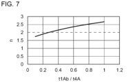
- FIG. 7 is a diagram showing the correlation between the ratio t1Ab/t4A of the thickness t1Ab of the optical waveguide to the thickness t4A of the first low dielectric constant layer and the effective refractive index n in the second embodiment.
- FIG. 8 is a cross-sectional view showing a schematic configuration of an optical modulator according to the third embodiment.
- FIG. 9 is a cross-sectional view showing a schematic configuration of an optical modulator according to the fourth embodiment.
- FIG. 10 is a diagram showing a modified example of the optical modulator according to the fourth embodiment.
- An optical modulator includes an optical waveguide, a first electrode, a second electrode, and a first low dielectric constant layer.
- the optical waveguide is made of a material having an electro-optic effect.
- the first electrode is made of a semiconductor material and is disposed with a gap between it and the optical waveguide.
- the second electrode is disposed so as to form a potential difference with the first electrode to apply an electric field to the optical waveguide.
- the first low dielectric constant layer has a refractive index smaller than the refractive index of the optical waveguide, and is disposed in the gap between the first electrode and the optical waveguide (first configuration).
- the first electrode is made of a semiconductor material among the first and second electrodes that apply an electric field to the optical waveguide.
- Semiconductor materials are usually doped with impurities.
- impurities In order to improve the function of the first electrode as an electrode, it is necessary to increase the amount of impurities doped. When the amount of impurities doped increases, the conductivity of the first electrode increases, but the light absorption rate of the first electrode increases.
- the refractive index of the first electrode made of a semiconductor material is greater than that of the optical waveguide, when the first electrode is in contact with the optical waveguide, light is likely to leak from the optical waveguide to the first electrode.
- the first electrode is arranged with a gap between it and the optical waveguide so that it is not in contact with the optical waveguide, and a first low dielectric layer with a refractive index smaller than that of the optical waveguide is arranged in the gap between the first electrode and the optical waveguide.
- a semiconductor material which is a material other than a metal material
- the optical modulator of the first configuration may further include a second low dielectric layer.
- the second low dielectric layer has a refractive index smaller than the refractive index of the optical waveguide.
- the second electrode is disposed with a gap between it and the optical waveguide, and the second low dielectric layer is provided in the gap between the second electrode and the optical waveguide (second configuration).
- the second electrode In the second configuration, of the first and second electrodes that apply an electric field to the optical waveguide, the second electrode is disposed with a gap between it and the optical waveguide. Therefore, the second electrode is not in contact with the optical waveguide. Furthermore, a second low dielectric layer with a smaller refractive index than the optical waveguide is disposed in the gap between the second electrode and the optical waveguide. This makes it difficult for light passing through the optical waveguide to leak to the second electrode side, and is also difficult for the light to be absorbed by the second electrode. Therefore, light loss can be further suppressed.
- the first low dielectric layer may surround the optical waveguide when viewed in a cross section perpendicular to the direction in which the optical waveguide extends, and may be provided between the optical waveguide and each of the first and second electrodes (third configuration).
- the first electrode is laminated on the optical waveguide
- the second electrode is laminated on the optical waveguide on the opposite side of the first electrode (fourth configuration).
- the optical waveguide exists between the first electrode and the second electrode in the lamination direction of the first electrode, the optical waveguide, and the second electrode. Therefore, an electric field from the first electrode and the second electrode can be efficiently applied to the optical waveguide.
- the ratio of the thickness of the first electrode to the thickness of the first low dielectric constant layer is 20.0 or more and 44.0 or less (fifth configuration). In this case, the generation of reflected waves of the electrical signal can be suppressed.
- the optical waveguide includes a substrate portion and a ridge portion protruding from the surface of the substrate portion.
- the first low dielectric constant layer is laminated on the substrate portion and the ridge portion, and the first electrode and the second electrode are laminated on the first low dielectric constant layer and may be arranged in parallel with a gap between them (sixth configuration).
- the ratio of the thickness of the first electrode to the thickness of the first low dielectric layer at the ridge portion is 0.1 or more and 4.0 or less (seventh configuration). In this case, the generation of reflected waves of the electrical signal can be suppressed.
- the size of the gap between the first electrode and the optical waveguide is preferably 0.750 ⁇ m or more and 1.675 ⁇ m or less (eighth configuration).
- evanescent light Light, although weak, seeps out from the optical waveguide into the first low dielectric layer provided in the gap between the first electrode and the optical waveguide. This seeping light is called evanescent light.
- the evanescent light is less likely to come into contact with the first electrode, and light loss can be further suppressed.
- the size of the gap between the first electrode and the optical waveguide is 1.675 ⁇ m or less.
- the distance between the first electrode and the optical waveguide is not too large, and the magnitude of the electric field for the optical waveguide can be ensured without increasing the voltage applied between the first electrode and the second electrode.
- the semiconductor material in the first electrode is preferably a silicon semiconductor material in which silicon is doped with impurities (ninth configuration).
- the impurity concentration in the first electrode is preferably 1.0 ⁇ 10 17 cm ⁇ 3 or more and 1.0 ⁇ 10 22 cm ⁇ 3 or less (tenth configuration).
- the resistivity decreases and the conductivity increases with an increase in the impurity. If the impurity concentration is 1.0 ⁇ 10 17 cm ⁇ 3 or more, the first electrode can effectively function as an electrode. If the impurity concentration is 1.0 ⁇ 10 22 cm ⁇ 3 or less, precipitation of the impurity can be prevented.
- the first electrode is preferably a silicon single crystal substrate (eleventh configuration).
- the main component of the first low dielectric constant layer may be SiO 2 (twelfth configuration). Since the semiconductor material used for the first electrode is a silicon semiconductor material, the first low dielectric constant layer of SiO 2 can be formed on the first electrode by a thermal oxidation method. In the film formation by the thermal oxidation method, the adhesion of the first low dielectric constant layer to the first electrode is good, and foreign matter is unlikely to enter the interface between the first electrode and the first low dielectric constant layer. Therefore, electrical loss can be suppressed at the interface between the first electrode and the first low dielectric constant layer. In addition, since the accumulation of foreign matter is suppressed at the interface between the first electrode and the first low dielectric constant layer, the reliability and life of the optical modulator can be improved.
- the refractive index of the first electrode is smaller than 3 (thirteenth configuration). In this case, the refractive index of the first electrode becomes smaller than 3, for example, in accordance with the impurity concentration (doping amount) of the tenth configuration.
- the surface layer of the first electrode on the optical waveguide side is preferably doped with impurities at a higher concentration than other parts of the first electrode (14th configuration).
- impurities at a higher concentration than other parts of the first electrode (14th configuration).
- a region of high conductivity can be localized in the first electrode near the optical waveguide, and attenuation of high-frequency signals can be suppressed by the skin effect.
- Fig. 1 is a cross-sectional view showing a schematic configuration of an optical modulator 10 according to a first embodiment.
- the optical modulator 10 includes an optical waveguide 1, a first electrode 2, a second electrode 3, a first low dielectric constant layer 4, and a second low dielectric constant layer 5.
- Fig. 1 shows a cross section perpendicular to the extension direction of the optical waveguide 1.
- the cross section means a cross section perpendicular to the extension direction of the optical waveguide 1, unless otherwise specified.
- the optical waveguide 1 may have a substantially rectangular cross section.
- the optical waveguide 1 is made of a material having an electro-optic effect (electro-optic material).
- the optical waveguide 1 functions as a light transmission path.
- LiNbO3 lithium niobate
- LiTaO3 lithium tantalate
- PLZT lead lanthanum zirconate titanate
- KTN potassium tantalate niobate
- BaTiO3 barium titanate
- an electro-optic polymer EO polymer
- the first electrode 2 and the second electrode 3 function as control electrodes for controlling light passing through the optical waveguide 1.
- Each of the first electrode 2 and the second electrode 3 may have a substantially rectangular cross section.
- the first electrode 2 and the second electrode 3 are arranged to form a potential difference between them to apply an electric field to the optical waveguide 1.
- the optical waveguide 1 is arranged between the first electrode 2 and the second electrode 3.
- the first electrode 2 is laminated on the optical waveguide 1.
- the second electrode 3 is laminated on the optical waveguide 1 on the opposite side of the first electrode 2. From another perspective, the first electrode 2 and the second electrode 3 are arranged so as to sandwich the optical waveguide 1.
- the first electrode 2 is disposed with a gap between it and the optical waveguide 1.
- the first electrode 2 is separated from the optical waveguide 1 in the stacking direction of the optical waveguide 1 and the electrodes 2 and 3.
- the first electrode 2 is not in contact with the optical waveguide 1.
- the size of the gap between the first electrode 2 and the optical waveguide 1 is, for example, 0.750 ⁇ m or more and 1.675 ⁇ m or less.
- the size of the gap between the first electrode 2 and the optical waveguide 1 means the shortest distance from the first electrode 2 to the optical waveguide 1.
- the distance in the stacking direction from the first electrode 2 to the optical waveguide 1 is the shortest distance from the first electrode 2 to the optical waveguide 1.
- the first electrode 2 is made of a semiconductor material. That is, the first electrode 2 is a semiconductor electrode.
- the semiconductor material used for the first electrode 2 is typically a silicon semiconductor material in which impurities are doped into Si (silicon).
- the semiconductor material for example, other single element semiconductors using Ge (germanium) or the like, or compound semiconductors such as GaAs (gallium arsenide) may be used.
- the impurities may be either p-type impurities or n-type impurities.
- a Group 3 element such as boron is used as the p-type impurity
- a Group 5 element such as phosphorus, arsenic, or antimony is used as the n-type impurity.
- the concentration (doping amount) of the impurity in the first electrode 2 is preferably 1.0 ⁇ 10 17 cm ⁇ 3 or more and 1.0 ⁇ 10 22 cm ⁇ 3 or less. As the doping amount of the impurity increases, the resistivity of the semiconductor material decreases and the conductivity increases. If the doping amount is 1.0 ⁇ 10 17 cm ⁇ 3 or more, the first electrode 2 can effectively function as an electrode. If the doping amount is 1.0 ⁇ 10 22 cm ⁇ 3 or less, the precipitation of the impurity can be prevented due to the solid solubility limit of the impurity in the silicon semiconductor material. As the doping amount increases, the refractive index of the first electrode 2 decreases. For example, the refractive index of the first electrode 2 is smaller than 3.
- the refractive index of the semiconductor material is larger than that of the electro-optical material constituting the optical waveguide 1, regardless of whether it is doped with impurities or not.
- the refractive index of the semiconductor material without doping with impurities is, for example, 3.4 for Si, 5.5 for Ge, and 3.3 for GaAs.
- the refractive index of the electro-optical material is, for example, 2.3 for LiNbO3, 2.8 for LiTaO3 , 2.5 for PLZT, 2.1 for KTN, and 2.6 for BaTiO3 .
- the refractive index of the semiconductor material decreases, but the refractive index of the semiconductor material after doping is also larger than that of the electro-optical material.
- the upper limit of the doping amount is preferably 1.0 ⁇ 10 22 cm ⁇ 3 is based on the solid solubility limit of impurities in silicon semiconductor materials. If the doping amount in the first electrode 2 exceeds the solid solubility limit of 1.0 ⁇ 10 22 cm ⁇ 3 , impurities will precipitate, and the reliability of the first electrode 2 and the optical modulator 10 will decrease.
- the reason why the lower limit of the doping amount is preferably 1.0 ⁇ 10 17 cm ⁇ 3 is as follows.
- the skin depth is an index for designing the thickness and width of the electrode. If the thickness and width of the electrode are smaller than the skin depth, the resistance value will increase.
- the thickness and width of the electrode is set to be equal to or greater than the skin depth.
- the doping amount is 1.0 ⁇ 10 17 cm ⁇ 3
- the conductivity is 1000 S/m
- the skin depth is 500 ⁇ m.
- the thickness of the electrode is limited to about 500 ⁇ m. From the viewpoint of ensuring the performance of the electrode, therefore, in order to obtain an electrode having a conductivity of 1000 S/m or more, the doping amount should be 1.0 ⁇ 10 17 cm ⁇ 3 or more.
- the first electrode 2 is, for example, a silicon single crystal substrate.
- impurities are doped in advance into a silicon single crystal base substrate that is the material of the first electrode 2.
- the first electrode 2 can be formed by placing this base substrate on another substrate and patterning (etching, dicing, etc.).
- the first electrode 2 may be an active layer of an SOI (Silicon on Insulator) substrate. In this case, the first electrode 2 can be formed by patterning (etching, dicing, etc.) the active layer of the SOI substrate. Impurities may be further introduced into the first electrode 2 thus formed by thermal diffusion, ion implantation, or the like.
- the first electrode 2 may be a semiconductor silicon layer formed on a substrate.
- a silicon layer can be formed on a substrate by sputtering, vapor deposition, CVD, or the like. Impurities can be introduced into this silicon layer by thermal diffusion, ion implantation, or the like to form a semiconductor silicon layer as the first electrode 2.
- the second electrode 3 is disposed with a gap between it and the optical waveguide 1.
- the second electrode 3 is separated from the optical waveguide 1 in the stacking direction.
- the second electrode 3 is not in contact with the optical waveguide 1.
- the size of the gap between the second electrode 3 and the optical waveguide 1 is, for example, 0.750 ⁇ m or more and 1.675 ⁇ m or less.
- the size of the gap between the second electrode 3 and the optical waveguide 1 means the shortest distance from the second electrode 3 to the optical waveguide 1.
- the distance in the stacking direction from the second electrode 3 to the optical waveguide 1 is the shortest distance from the second electrode 3 to the optical waveguide 1.
- the second electrode 3 is made of, for example, a metal material. That is, the second electrode 3 is a metal electrode. However, the second electrode 3 may be made of, for example, a semiconductor material. That is, the second electrode 3 may be a semiconductor electrode. Examples of semiconductor materials include those similar to those used for the first electrode 2.
- the main component of the metal material is, for example, a precious metal.
- the precious metal is, for example, Au (gold).
- As the precious metal Ag (silver), Pt (platinum), etc. may be used.
- the metal material may contain trace amounts of other metal elements such as Cr and Ti.
- As the metal material copper, aluminum, or an alloy thereof, etc. may be used.
- the second electrode 3 is used as a signal electrode, and the first electrode 2 is used as a ground electrode. Conversely, the first electrode 2 may be used as a signal electrode, and the second electrode 3 may be used as a ground electrode.
- the first low dielectric layer 4 is provided in the gap between the first electrode 2 and the optical waveguide 1.
- the first low dielectric layer 4 is laminated on the first electrode 2, and the optical waveguide 1 is laminated on the first low dielectric layer 4.
- the optical waveguide 1 is indirectly laminated on the first electrode 2 via the first low dielectric layer 4, and the first electrode 2 is not in contact with the optical waveguide 1. It is preferable that the first low dielectric layer 4 covers the entire surface of the optical waveguide 1 facing the first low dielectric layer 4.
- the first low dielectric constant layer 4 has a refractive index smaller than that of the optical waveguide 1.
- the refractive index of the first low dielectric constant layer 4 is smaller than that of the optical waveguide 1 by 1% or more.
- the refractive index of the optical waveguide 1 is smaller than that of the first electrode 2.
- the ratio of the refractive index of the optical waveguide 1 to that of the first low dielectric constant layer 4 is, for example, 1.8 or more and 2.5 or less. In this case, light can be sufficiently confined within the optical waveguide 1.
- the ratio of the refractive index of the first electrode 2 to that of the first low dielectric constant layer 4 is, for example, 1.5 or more and 6.0 or less. In this case, when light enters the optical waveguide 1 from the optical fiber, it is possible to prevent light from entering the first electrode 2.
- the main component of the first low dielectric constant layer 4 is typically SiO 2.
- the main component of the first low dielectric constant layer 4 may be an oxide such as Al 2 O 3 , LaAlO 3 , LaYO 3 , ZnO, HfO 2 , MgO, or Y 2 O 3 , or a polymer such as BCB (benzocyclobutene) or PI (polyimide).
- the second low dielectric layer 5 is provided in the gap between the second electrode 3 and the optical waveguide 1.
- the second low dielectric layer 5 is laminated on the optical waveguide 1, and the second electrode 3 is laminated on the second low dielectric layer 5.
- the optical waveguide 1 is indirectly laminated on the second electrode 3 via the second low dielectric layer 5, and the second electrode 3 is not in contact with the optical waveguide 1. It is preferable that the second low dielectric layer 5 covers the entire surface of the optical waveguide 1 facing the second low dielectric layer 5.
- the second low dielectric layer 5 has a refractive index smaller than that of the optical waveguide 1.
- Examples of the main component of the second low dielectric layer 5 include those similar to those of the first low dielectric layer 4 described above.
- the main component of the second low dielectric layer 5 may be the same as or different from the main component of the first low dielectric layer 4.
- the second electrode 3 can be laminated on the optical waveguide 1 and the first electrode 2, for example, as follows.
- the first low dielectric layer 4 is formed on the first electrode 2 by CVD, vapor deposition, sputtering, etc.
- a material substrate having an electro-optic effect is placed on the first low dielectric layer 4 formed on the first electrode 2, and the material substrate is bonded to the first low dielectric layer 4.
- lithography and etching are performed on the material substrate to form the optical waveguide 1.
- the second low dielectric layer 5 is formed on the optical waveguide 1 by CVD, vapor deposition, sputtering, etc.
- a metal layer is formed on the second low dielectric layer 5 by sputtering, vapor deposition, etc.
- the formed metal layer is patterned by lithography, and the second electrode 3 is formed by etching.
- the thickness t2 required for the first electrode 2 can be estimated based on the skin effect.
- the thickness t2 of the first electrode 2 corresponds to the length in the stacking direction.
- the following formula (1) is used to calculate the skin depth of a conductor.
- the thickness t2 required for the first electrode 2 can be determined. More specifically, by making the thickness t2 of the first electrode 2 larger than the skin depth calculated using formula (1), the electrical resistance of the first electrode 2 can be reduced, and excess electrical loss can be suppressed. The higher the electrical conductivity of the first electrode 2, the more preferable it is. However, since there is a solid solubility limit for the doping amount of the impurity, and since the impurity clusters when the doping amount approaches the solid solubility limit, and a state in which it becomes inactive as a carrier occurs, the electrical conductivity of the first electrode 2 is saturated when the doping amount exceeds a certain amount.
- the electrical conductivity of the first electrode 2 is 1 ⁇ 10 7 S/m, and the skin depth of the 1 GHz electrical signal is 5 ⁇ m.
- the actual electrical conductivity will be about 1 ⁇ 10 6 S/m, which is one order of magnitude lower.
- the thickness t2 of the first electrode 2 is 25 ⁇ m or more.
- the ratio Z/Z0 of the resistance Z of the optical modulator 10 to the termination resistance Z0 is preferably 0.8 or more and 1.2 or less. If the ratio Z/Z0 is out of the condition of 0.8 or more and 1.2 or less, a reflected wave of the electrical signal is generated at the end of the electrode due to an impedance mismatch. Therefore, it is preferable to set the various conditions of the optical modulator 10 so that the ratio Z/Z0 satisfies this condition.
- the ratio t2/t4 of the thickness t2 of the first electrode 2 is set to the thickness t4 of the first low dielectric layer 4 so that the ratio Z/Z0 of the resistance Z of the optical modulator 10 to the termination resistance Z0 is 0.8 or more and 1.2 or less.
- the thickness t4 of the first low dielectric layer 4 corresponds to the size of the gap between the first electrode 2 and the optical waveguide 1.
- FIG. 2 is a diagram showing the correlation between the ratio t2/t4 of the thickness t2 of the first electrode 2 to the thickness t4 of the first low dielectric layer 4, and the ratio Z/Z0 of the resistance Z of the optical modulator 10 to the termination resistance Z0.
- Fig. 2 shows the relationship between the ratio t2/t4 and the ratio Z/Z0 when an analysis is performed using a silicon semiconductor material as the first electrode 2, a metal material containing Au as the main component as the second electrode 3 , SiO2 as the low dielectric layers 4 and 5, and LiNbO3 as the optical waveguide 1.
- the termination resistance Z0 was set to 50 ⁇
- the width w2 of the first electrode 2 was set to 50 ⁇ m
- the width w3 of the second electrode 3 was set to 40 ⁇ m
- the thickness t3 of the second electrode 3 was set to 5.0 ⁇ m
- the thickness t4 of the first low dielectric constant layer 4 was set to 0.7 ⁇ m
- the thickness t5 of the second low dielectric constant layer 5 was set to 0.7 ⁇ m
- the width w1 of the optical waveguide 1 was set to 1.0 ⁇ m
- the thickness t1 of the optical waveguide 1 was set to 1.3 ⁇ m.
- the thickness means the length in the stacking direction in the cross section of the optical modulator 10
- the width means the length in the direction perpendicular to the stacking direction in the cross section of the optical modulator 10.
- the ratio t2/t4 of the thickness t2 of the first electrode 2 to the thickness t4 of the first low dielectric constant layer 4 is 20.0 or more and 44.0 or less.
- the first electrode 2 is formed of a semiconductor material.
- a metal material is used as the material of the second electrode 3
- the performance of the first electrode 2 as an electrode is equivalent to that of the second electrode 3, which is a metal electrode.
- the cross-sectional areas of the first electrode 2 and the second electrode 3 are preferably set so that the resistance value of the first electrode 2 substantially matches the resistance value of the second electrode 3.
- the cross-sectional area of the first electrode 2 can be "(conductivity of the second electrode 3/conductivity of the first electrode 2) x cross-sectional area of the second electrode 3".
- the area of the first electrode 2 is preferably larger than the area of the second electrode 3.
- the second electrode 3 is made of a metal material, the second electrode 3 has a relatively small resistance value even without a large cross-sectional area.
- the first electrode 2 is made of a semiconductor material that has a lower conductivity than a metal material, by making the cross-sectional area larger than that of the second electrode 3, the resistance value can be reduced to the same level as that of the second electrode 3. This makes it possible to reduce power consumption.
- the resistance value of the first electrode 2, which is a semiconductor electrode is made to coincide with the resistance value of the second electrode 3, which is a metal electrode, so that the product of the conductivity and the thickness t2 of the first electrode 2 may coincide with the product of the conductivity and the thickness t3 of the second electrode 3.
- the metal material of the second electrode 3 is Au
- the thickness t3 of the second electrode 3 is usually set to 0.1 ⁇ m or more and 2.0 ⁇ m or less, and the conductivity is 4.3 ⁇ 10 7 S/m.
- the conductivity of the first electrode 2 is smaller than that of the second electrode 3, the thickness t2 of the first electrode 2 is larger than the thickness t3 of the second electrode 3.
- the conductivity of the first electrode 2 changes depending on the amount of impurities doped.
- the conductivity of the first electrode 2 is 1 ⁇ 10 7 S/m.
- the value obtained by dividing the conductivity of the second electrode 3 by the conductivity of the first electrode 2 is 4.3, and the thickness t2 of the first electrode 2 can be set to 4.3 times the thickness t3 of the second electrode 3.
- the doping amount of the impurity is the lower limit of 1.0 ⁇ 10 17 cm ⁇ 3
- the conductivity of the first electrode 2 is 1000 ⁇ 10 4 S/m.
- the value obtained by dividing the conductivity of the second electrode 3 by the conductivity of the first electrode 2 is 4.3 ⁇ 10 3
- the thickness t2 of the first electrode 2 can be set to 4.3 ⁇ 10 3 times the thickness t3 of the second electrode 3.
- the lower limit of the thickness t2 of the first electrode 2 can be 4.3 times the lower limit of the thickness t3 of the second electrode 3, which is 0.1 ⁇ m. That is, the thickness t2 of the first electrode 2 can be 0.43 ⁇ m or more.
- the upper limit of the thickness t2 of the first electrode 2 can be 4.3 ⁇ 10 3 times the upper limit of the thickness t3 of the second electrode 3, which is 2.0 ⁇ m. That is, the thickness t2 of the first electrode 2 can be 8600 ⁇ m (8.6 mm) or less.
- the thickness t2 of the first electrode 2 is 500 ⁇ m or less from the viewpoint of its processability.
- the second electrode 3 can also be made of a semiconductor material.
- the area of the first electrode 2 is the same as the area of the second electrode 3 when viewed in a cross section perpendicular to the extension direction of the optical waveguide 1.
- the thickness t2 of the first electrode 2, which is a semiconductor electrode, and the thickness t4 of the low dielectric layer 4 can be measured, for example, by the following methods.
- the first method is a measurement method using SEM observation.
- the optical modulator 10 is cut using a FIB (focused ion beam) to obtain a sample.
- the cross section of the obtained sample is imaged using an SEM, and the thickness t2 of the first electrode 2 and the thickness t4 of the low dielectric layer 4 can be measured from the obtained image.
- the second method is an optical measurement method. In this method, the thickness t2 of the first electrode 2 and the thickness t4 of the low dielectric layer 4 can be directly measured using interference spectroscopy. Either method produces substantially the same measurement results.
- the thickness t3 of the second electrode 3 can be measured, for example, by the following methods.
- the first method is the measurement method using SEM observation described above.
- the second method is a measurement method using X-rays. In this method, the second electrode 3 is irradiated with X-rays, and the amount of X-rays that penetrate is measured to determine the amount of attenuation by the second electrode 3.
- the thickness t3 of the second electrode 3 can be measured by back-calculating the determined amount of attenuation. Either method will produce substantially the same measurement results.
- the second electrode 3 is a semiconductor electrode
- the thickness t3 of the second electrode 3 can be measured by the method for measuring the thickness t2 of the first electrode 2 described above.
- the amount of doping in the first electrode 2 can be measured by epitaxial resistivity measurement, air gap CV measurement, mercury CV measurement, surface charge profiling, secondary ion mass spectrometry, spreading resistance measurement, etc.
- the measurement results are essentially the same regardless of the method.
- the width w2 of the first electrode 2 on the optical waveguide 1 side is preferably larger than the width w1 of the optical waveguide 1.
- the width w2 of the first electrode 2 on the optical waveguide 1 side refers to the width of the surface of the first electrode 2 closest to the optical waveguide 1.
- the length of the surface of the first electrode 2 in contact with the first low dielectric layer 4 in the direction perpendicular to the stacking direction is width w2. In this case, an electric field can be applied to the entire optical waveguide 1.
- the first electrode 2 is made of a semiconductor material among the first electrode 2 and the second electrode 3 that apply an electric field to the optical waveguide 1.
- the semiconductor material is usually doped with impurities.
- impurities In order to improve the function of the first electrode 2 as an electrode, it is necessary to increase the amount of impurities doped. When the amount of impurities doped increases, the conductivity of the first electrode 2 increases, but the light absorption rate of the first electrode 2 increases.
- the refractive index of the first electrode 2 made of a semiconductor material is larger than that of the optical waveguide 1, when the first electrode 2 is in contact with the optical waveguide 1, light is likely to leak from the optical waveguide 1 to the first electrode 2.
- the first electrode 2 is arranged with a gap between it and the optical waveguide 1 so as to be out of contact with the optical waveguide 1, and a first low dielectric layer 4 having a refractive index smaller than that of the optical waveguide 1 is arranged in the gap between the first electrode 2 and the optical waveguide 1.
- the optical modulator 10 of this embodiment it is possible to suppress optical loss while realizing the application of a semiconductor material, which is a material other than a metal material, to the first electrode 2 .
- the effective refractive index of the electrical signal (modulation wave (GHz)) applied from the electrode to the optical waveguide is greater than the effective refractive index of the light wave (carrier wave (THz)) passing through the optical waveguide. If the effective refractive index of the electrical signal is significantly different from the effective refractive index of the light wave, the difference between the propagation speed of the light wave and the propagation speed of the electrical signal becomes large, and the modulation speed decreases.
- the first low dielectric constant layer 4 is disposed at least between the first electrode 2 and the optical waveguide 1, so that it is possible to adjust the cross-sectional area ratio of the first low dielectric constant layer 4 to the optical waveguide 1.
- the difference between the effective refractive index of the electrical signal and the effective refractive index of the light wave can be reduced, and as a result, the difference between the propagation speed of the light wave and the propagation speed of the electrical signal can be reduced. This makes it possible to suppress a decrease in the modulation speed.
- the second electrode 3 is disposed with a gap between it and the optical waveguide 1. In this case, the second electrode 3 is not in contact with the optical waveguide 1. Furthermore, a second low dielectric layer 5 having a smaller refractive index than the optical waveguide 1 is provided in the gap between the second electrode 3 and the optical waveguide 1. This makes it difficult for light passing through the optical waveguide 1 to leak to the second electrode 3 side, and is also difficult for it to be absorbed by the second electrode 3. Therefore, light loss can be suppressed.
- the semiconductor material used for the first electrode 2 is, for example, a silicon semiconductor material in which impurities are doped into Si.
- the first electrode 2 may be a silicon single crystal substrate, or a semiconductor silicon layer formed on a substrate.
- the internal stress of the first electrode 2 can be reduced compared to a metal electrode formed by sputtering, vapor deposition, or the like. Therefore, it is possible to form the first electrode 2 thick while suppressing the internal stress of the first electrode 2.
- the resistance value of the first electrode 2 is reduced, and power consumption can be suppressed.
- the internal stress of the first electrode 2 the occurrence of cracks due to internal stress can be suppressed. As a result, failure and damage to the optical modulator 10 can be suppressed.
- Silicon semiconductor materials are less expensive than, for example, metallic materials using precious metals. Therefore, by forming the first electrode 2 from a silicon semiconductor material, it is possible to reduce the cost of the optical modulator 10.
- the first electrode 2 is laminated on the optical waveguide 1
- the second electrode 3 is laminated on the optical waveguide 1 on the opposite side of the first electrode 2.
- the optical waveguide 1 exists between the first electrode 2 and the second electrode 3 in the lamination direction. Therefore, an electric field from the first electrode 2 and the second electrode 3 can be efficiently applied to the optical waveguide 1.
- the semiconductor material used for the first electrode 2 is a silicon semiconductor material
- the first low dielectric constant layer 4 of SiO 2 can be formed on the first electrode 2 by a thermal oxidation method.
- the adhesion of the first low dielectric constant layer 4 to the first electrode 2 is good, and foreign matter is unlikely to enter the interface between the first electrode 2 and the first low dielectric constant layer 4. Therefore, electrical loss can be suppressed at the interface between the first electrode 2 and the first low dielectric constant layer 4.
- the reliability and life of the optical modulator 10 can be improved. This is because if foreign matter accumulates at the interface between the first electrode 2 and the first low dielectric constant layer 4 and an electric field concentrates on the accumulated foreign matter, the optical modulator 10 may be damaged.
- the penetration depth of the evanescent light in each of the low dielectric layers 4, 5 can be estimated using the wavelength of the light (carrier wave) passing through the optical waveguide 1 as a guide.
- the evanescent light can be prevented from contacting each of the electrodes 2, 3. Therefore, it is preferable that the size of the gap between the optical waveguide 1 and each of the electrodes 2, 3, i.e., the thicknesses t4, t5 (length in the stacking direction) of each of the low dielectric layers 4, 5, be equal to or greater than the wavelength of the light passing through the optical waveguide 1.
- the size of the gap between each of the electrodes 2, 3 and the optical waveguide 1 may be 0.750 ⁇ m or more. If the size of the gap between each of the electrodes 2, 3 and the optical waveguide 1 is 1.675 ⁇ m or less, the magnitude of the electric field for the optical waveguide 1 can be ensured without increasing the voltage applied between the first electrode 2 and the second electrode 3.
- FIG. 3 shows a first modified example of the optical modulator 10 according to the first embodiment.
- the optical modulator 10 may not include the second low dielectric layer 5 (FIG. 1). That is, the second electrode 3 may be directly laminated on the optical waveguide 1 and may be in contact with the optical waveguide 1.
- the dimensional relationship between the first electrode 2, which is a semiconductor electrode, and the first low dielectric layer 4 can be determined as described above.
- the ratio t2/t4 of the thickness t2 of the first electrode 2 to the thickness t4 of the first low dielectric layer 4 is set so that the ratio Z/Z0 of the resistance Z of the optical modulator 10 to the termination resistance Z0 is 0.8 or more and 1.2 or less.
- FIG. 4 shows a second modified example of the optical modulator 10 according to the first embodiment.
- the second low dielectric layer 5 (FIG. 1) is not provided in the optical modulator 10, as in the example shown in FIG. 3.
- the first low dielectric layer 4 is provided so as to surround the optical waveguide 1 in a cross-sectional view of the optical modulator 10.
- the first low dielectric layer 4 is provided not only between the first electrode 2 and the optical waveguide 1, but also between the second electrode 3 and the optical waveguide 1. That is, the first electrode 2 and the second electrode 3 are not in contact with the optical waveguide 1, and the first low dielectric layer 4 is interposed between each of the first electrode 2 and the second electrode 3 and the optical waveguide 1.
- the first low dielectric layer 4 can also serve as the second low dielectric layer 5 (FIG. 1).
- Second Embodiment 5 is a cross-sectional view showing a schematic configuration of an optical modulator 10A according to the second embodiment.
- the optical modulator 10A differs from the optical modulator 10 according to the first embodiment in the configuration of an optical waveguide 1A and the arrangement of a first electrode 2A and a second electrode 3A.
- the optical modulator 10A includes an optical waveguide 1A, a first electrode 2A, a second electrode 3A, and a first low dielectric layer 4A.
- the optical waveguide 1A includes a substrate portion 1Aa and a ridge portion 1Ab.
- the ridge portion 1Ab protrudes from the surface of the substrate portion 1Aa.
- the ridge portion 1Ab essentially functions as an optical waveguide.
- a first low dielectric layer 4A is laminated on the optical waveguide 1A. More specifically, the first low dielectric layer 4A is laminated on the substrate portion 1Aa and the ridge portion 1Ab.
- the first electrode 2A and the second electrode 3A are stacked on the first low dielectric layer 4A.
- the first electrode 2A and the second electrode 3A are arranged in parallel with a gap between them.
- the first electrode 2A and the second electrode 3A are arranged side by side in a direction substantially perpendicular to the stacking direction of the optical waveguide 1A and the first low dielectric layer 4A in a cross-sectional view of the optical modulator 10A.
- the first electrode 2A is arranged on one side of the ridge portion 1Ab
- the second electrode 3A is arranged on the other side of the ridge portion 1Ab.
- the first electrode 2A and the second electrode 3A can form a potential difference between each other to apply an electric field to the ridge portion 1Ab of the optical waveguide 1A.
- the optical modulator 10A according to this embodiment can achieve the same effects as the optical modulator 10 according to the first embodiment.
- the ratio Z/Z0 of the resistance Z of the optical modulator 10A to the termination resistance Z0 is 0.8 or more and 1.2 or less. Therefore, it is preferable that the ratio t2A/t4A of the thickness t2A of the first electrode 2A to the thickness t4A of the first low-dielectric layer 4A is set so that the ratio Z/Z0 of the resistance Z of the optical modulator 10 to the termination resistance Z0 is 0.8 or more and 1.2 or less.
- the thickness t4A of the first low-dielectric layer 4A in this embodiment is the thickness of the first low-dielectric layer 4A at the position of the ridge portion 1Ab.
- the thickness t4A refers to the shortest distance from the interface between the ridge portion 1Ab and the first low-dielectric layer 4A to the interface between the first low-dielectric layer 4A and the first electrode 2A in the stacking direction of the ridge portion 1Ab, the first low-dielectric layer 4A, and the electrodes 2A and 2B.
- Fig. 6 is a diagram showing the correlation between the ratio t2A/t4A of the thickness t2A of the first electrode 2A to the thickness t4A of the first low dielectric constant layer 4A and the ratio Z/Z0 of the resistance Z of the optical modulator 10A to the termination resistance Z0 in the second embodiment.
- Fig. 6 shows the relationship between the ratio t2A/t4A and the ratio Z / Z0 when an analysis is performed using a silicon semiconductor material as the first electrode 2A, a metal material containing Au as the main component as the second electrode 3A, SiO2 as the first low dielectric constant layer 4A, and LiNbO3 as the optical waveguide 1A, as an example.
- the termination resistance Z0 was set to 50 ⁇
- the width w2A of the first electrode 2A was set to 50 ⁇ m
- the width w3A of the second electrode 3A was set to 21.5 ⁇ m
- the thickness t3A of the second electrode 3A was set to 16.6 ⁇ m
- the thickness t4A of the first low dielectric constant layer 4A was set to 8.3 ⁇ m
- the width w1Ab of the ridge portion 1Ab was set to 2.0 ⁇ m
- the thickness t1Ab of the ridge portion 1Ab was set to 1.0 ⁇ m
- the gap g between the first electrode 2A and the second electrode 3A was set to 10 ⁇ m.
- the ratio t2A/t4A of the thickness t2A of the first electrode 2A to the thickness t4A of the first low dielectric constant layer 4A is 0.1 or more and 4.0 or less.
- the effective refractive index n is a value that maximizes the modulation speed. Therefore, it is preferable that the ratio t1Ab/t4A of the thickness t1Ab of the optical waveguide 1A (ridge portion 1Ab) to the thickness t4A of the first low dielectric layer 4A is set so that the effective refractive index n is a value that maximizes the modulation speed.
- FIG. 7 is a diagram showing the correlation between the ratio t1Ab/t4A of the thickness t1Ab of the optical waveguide 1A to the thickness t4A of the first low dielectric constant layer 4A and the effective refractive index n in the second embodiment.
- FIG. 7 shows the relationship between the ratio t1Ab/t4A and the effective refractive index n when an analysis is performed under the same conditions as in FIG. 6.
- the thickness t2A of the first electrode 2A is set to 16.6 ⁇ m.
- the modulation speed can be maximized if the effective refractive index n is 2.
- the ratio t1Ab/t4A of the thickness t1Ab of the optical waveguide 1A (ridge portion 1Ab) to the thickness t4A of the first low dielectric constant layer 4A is substantially 0.28.
- Third Embodiment 8 is a cross-sectional view showing a schematic configuration of an optical modulator 10B according to the third embodiment.
- the optical modulator 10B differs from the optical modulator 10 according to the first embodiment in the configuration of the first electrode 2B.
- the first electrode 2B has a surface layer 2Ba on the optical waveguide 1 side and a remaining portion 2Bb.
- the surface layer 2Ba is disposed so as to be adjacent to the first low dielectric constant layer 4 of the first electrode 2B.
- the surface layer 2Ba is, for example, a portion within a range of 10% of the length (thickness) of the first electrode 2B in the stacking direction of the first electrode 2B relative to the optical waveguide 1 from the surface of the first electrode 2B on the optical waveguide 1 side.
- the remaining portion 2Bb refers to the portion of the first electrode 2B excluding the surface layer 2Ba.
- the concentration of the impurity doped in the semiconductor material is higher in the surface layer 2Ba than in the remaining portion 2Bb. That is, the first electrode 2B has different impurity concentrations, i.e., dopant amounts, between the surface layer 2Ba and the remaining portion 2Bb.
- the impurity concentration in the surface layer 2Ba is 10% or more higher than the impurity concentration in the remaining portion 2Bb.
- Such an impurity concentration distribution in the first electrode 2B can be formed by thermal diffusion or ion implantation, etc.
- the impurity concentration may change suddenly at the boundary between the surface layer 2Ba and the remaining portion 2Bb, or may gradually decrease as it moves away from the surface layer 2Ba in the stacking direction.
- the impurity concentration in the first electrode 2B can be measured by epitaxial resistivity measurement, air gap CV measurement, mercury CV measurement, surface charge profiling, secondary ion mass spectrometry, spreading resistance measurement, etc. The measurement results are substantially the same regardless of the method.
- the difference between the impurity concentration in the surface layer 2Ba and the impurity concentration in the remaining portion 2Bb can be confirmed by any of the above measurement methods.
- a profile of the impurity concentration in the depth direction from the surface on the optical waveguide 1 side of the first electrode 2B is obtained.
- the integral average of the impurity concentration in the surface layer 2Ba and the integral average of the impurity concentration in the remaining portion 2Bb are calculated, and are defined as the impurity concentration in the surface layer 2Ba and the impurity concentration in the remaining portion 2Bb, respectively.
- the integral average of the impurity concentration in the range from the surface of the first electrode 2B on the optical waveguide 1 side to 10% of the depth (thickness) of the first electrode 2B is the impurity concentration of the surface layer 2Ba
- the integral average of the impurity concentration in the remaining range is the impurity concentration of the remaining portion 2Bb.
- the impurity concentration of the obtained surface layer 2Ba is, for example, 10% or more higher than the impurity concentration of the obtained remaining portion 2Bb.
- the conductivity near the surface layer 2Ba is higher.
- the surface layer 2Ba of the first electrode 2B on the optical waveguide 1 side is doped with impurities at a higher concentration than the remaining portion 2Bb of the first electrode 2. In this case, a region of high conductivity can be localized near the optical waveguide 1 in the first electrode 2B, and attenuation of the high frequency signal can be suppressed due to the skin effect.
- Fourth Embodiment 9 is a cross-sectional view showing a schematic configuration of an optical modulator 10C according to the fourth embodiment.
- the optical modulator 10C differs from the optical modulator 10A according to the second embodiment in the configuration of a first electrode 2C.
- the first electrode 2C has a surface layer 2Ca on the ridge portion 1Ab side of the optical waveguide 1A, and a remaining portion 2Cb.
- the surface layer 2Ca on the ridge portion 1Ab side is the surface layer of the first electrode 2C through which the electric field applied to the ridge portion 1Ab passes together with the second electrode 3A.
- the surface layer 2Ca is the surface layer of the first electrode 2C located on the ridge portion 1Ab side that essentially functions as an optical waveguide in a direction (width direction) perpendicular to the stacking direction of the first electrode 2C with respect to the optical waveguide 1A.
- the surface layer 2Ca is, for example, a portion within a range of 10% of the width direction length of the first electrode 2C from the surface positioned on the ridge portion 1Ab side in the width direction of the first electrode 2C.
- the remaining portion 2Cb refers to the portion of the first electrode 2C excluding the surface layer 2Ca.
- the concentration of impurities doped into the semiconductor material is higher in the surface layer 2Ca than in the remaining portion 2Cb. Therefore, the optical modulator 10C of this embodiment can achieve the same effects as the optical modulator 10B of the third embodiment.
- FIG. 10 shows a modified example of the optical modulator 10C according to the fourth embodiment.
- the surface layer 2Ca may be the surface layer of the first electrode 2C that is located on the optical waveguide 1A side in the stacking direction of the first electrode 2C relative to the optical waveguide 1.
- the surface layer 2Ca is, for example, a portion that is within a range of 10% of the thickness of the first electrode 2C from the surface that is located on the optical waveguide 1A side in the stacking direction. Even with this configuration, the same effect as the optical modulator 10B according to the third embodiment can be achieved.
- the first electrode 2 may include a convex portion.
- the convex portion is provided on the surface located on the optical waveguide 1 side in the stacking direction, and protrudes toward the optical waveguide 1.
- the convex portion contacts the first low dielectric layer 4.
- the convex portion can concentrate the electric field on the optical waveguide. This allows the voltage applied between the first electrode 2 and the second electrode 3 to be reduced, further reducing power consumption.
- the length of the convex portion in a direction perpendicular to the stacking direction when viewed in a cross section perpendicular to the extension direction of the optical waveguide 1 may be smaller the closer it is to the optical waveguide 1.
- the side of the convex portion can be made to continue relatively gently with other parts of the surface of the first electrode 2 on the optical waveguide 1 side. This makes it possible to prevent electrical loss at the boundary between the convex portion and other parts.
- the side of the convex portion may be inclined at a constant gradient relative to the surface, or the gradient of the side surface relative to the surface may vary.
- the optical modulator 10 according to the first embodiment may further include a thin metal film thinner than the first electrode 2.
- the thin metal film is provided on the surface of the first electrode 2 facing the optical waveguide 1.
- the thin metal layer has high conductivity and low attenuation of high-frequency signals.
- the thin metal layer may be formed, for example, using a metal material that can be used for the second electrode 3.
- the thin metal layer may be applied to each of the optical modulators 10A, 10B, and 10C according to the second to fourth embodiments. In this case, the thin metal layer is provided on the surface of the first electrodes 2A, 2B, and 2C where the electric field passes.
- an optical waveguide made of a material having an electro-optic effect
- a first electrode made of a semiconductor material and disposed with a gap between the first electrode and the optical waveguide
- a second electrode disposed to form a potential difference with the first electrode to apply an electric field to the optical waveguide
- a first low dielectric constant layer having a refractive index smaller than a refractive index of the optical waveguide and provided in the gap between the first electrode and the optical waveguide.
- the optical modulator according to ⁇ 1> further comprising: a second low dielectric constant layer having a refractive index smaller than the refractive index of the optical waveguide; the second electrode is disposed with a gap between it and the optical waveguide, The second low dielectric constant layer is provided in the gap between the second electrode and the optical waveguide.
- ⁇ 3> The optical modulator according to ⁇ 1>, an optical modulator, wherein the first low dielectric constant layer surrounds the optical waveguide when viewed in a cross section perpendicular to an extension direction of the optical waveguide, and is provided between the optical waveguide and each of the first electrode and the second electrode.
- ⁇ 4> An optical modulator according to any one of ⁇ 1> to ⁇ 3>, the first electrode is laminated on the optical waveguide; The second electrode is laminated to the optical waveguide on an opposite side to the first electrode.
- ⁇ 5> The optical modulator according to ⁇ 4>, An optical modulator, wherein a ratio of a thickness of the first electrode to a thickness of the first low dielectric constant layer is not less than 20.0 and not more than 44.0.
- the optical waveguide includes a substrate and a ridge portion protruding from a surface of the substrate; the first low dielectric constant layer is laminated on the substrate portion and the ridge portion, The first electrode and the second electrode are stacked on the first low dielectric constant layer and arranged in parallel with a gap between them.
- ⁇ 7> The optical modulator according to ⁇ 6>, an optical modulator, wherein a ratio of a thickness of the first electrode to a thickness of the first low dielectric constant layer at the position of the ridge portion is not less than 0.1 and not more than 4.0.
- An optical modulator according to any one of ⁇ 1> to ⁇ 7>, An optical modulator, wherein the size of the gap between the first electrode and the optical waveguide is not less than 0.750 ⁇ m and not more than 1.675 ⁇ m.
- An optical modulator according to any one of ⁇ 1> to ⁇ 8>, An optical modulator, wherein the semiconductor material is a silicon semiconductor material in which silicon is doped with an impurity.
- ⁇ 10> The optical modulator according to ⁇ 9>, An optical modulator, wherein a concentration of the impurity in the first electrode is not less than 1.0 ⁇ 10 17 cm ⁇ 3 and not more than 1.0 ⁇ 10 22 cm ⁇ 3 .
- Optical modulator 1A Optical waveguide 1Aa: Substrate portion 1Ab: Ridge portion 2, 2A, 2B, 2C: First electrode 2Ba, 2Ca: Surface layer 2Bb, 2Cb: Remaining portion 3, 3A: Second electrode 4, 4A: First low dielectric constant layer 5: Second low dielectric constant layer
Landscapes
- Physics & Mathematics (AREA)
- Nonlinear Science (AREA)
- Engineering & Computer Science (AREA)
- General Physics & Mathematics (AREA)
- Optics & Photonics (AREA)
- Chemical & Material Sciences (AREA)
- Ceramic Engineering (AREA)
- Crystallography & Structural Chemistry (AREA)
- Microelectronics & Electronic Packaging (AREA)
- Optical Modulation, Optical Deflection, Nonlinear Optics, Optical Demodulation, Optical Logic Elements (AREA)
Priority Applications (4)
| Application Number | Priority Date | Filing Date | Title |
|---|---|---|---|
| JP2024532172A JP7729490B2 (ja) | 2022-11-30 | 2023-06-21 | 光変調器 |
| CN202380070802.7A CN119948390A (zh) | 2022-11-30 | 2023-06-21 | 光调制器 |
| US18/768,275 US20240361624A1 (en) | 2022-11-30 | 2024-07-10 | Optical modulator |
| JP2025134627A JP2025166143A (ja) | 2022-11-30 | 2025-08-13 | 光変調器 |
Applications Claiming Priority (2)
| Application Number | Priority Date | Filing Date | Title |
|---|---|---|---|
| JP2022-192105 | 2022-11-30 | ||
| JP2022192105 | 2022-11-30 |
Related Child Applications (1)
| Application Number | Title | Priority Date | Filing Date |
|---|---|---|---|
| US18/768,275 Continuation US20240361624A1 (en) | 2022-11-30 | 2024-07-10 | Optical modulator |
Publications (1)
| Publication Number | Publication Date |
|---|---|
| WO2024116446A1 true WO2024116446A1 (ja) | 2024-06-06 |
Family
ID=91323194
Family Applications (1)
| Application Number | Title | Priority Date | Filing Date |
|---|---|---|---|
| PCT/JP2023/022845 Ceased WO2024116446A1 (ja) | 2022-11-30 | 2023-06-21 | 光変調器 |
Country Status (4)
| Country | Link |
|---|---|
| US (1) | US20240361624A1 (https=) |
| JP (2) | JP7729490B2 (https=) |
| CN (1) | CN119948390A (https=) |
| WO (1) | WO2024116446A1 (https=) |
Citations (4)
| Publication number | Priority date | Publication date | Assignee | Title |
|---|---|---|---|---|
| JP2002244168A (ja) * | 2001-02-21 | 2002-08-28 | Fuji Xerox Co Ltd | 光スイッチの設計方法及び光スイッチ |
| US20040066250A1 (en) * | 2000-08-25 | 2004-04-08 | Hunt Andrew T | Electronic and optical devices and methods of forming these devices |
| JP2004325536A (ja) * | 2003-04-22 | 2004-11-18 | Sun Tec Kk | 非線形光デバイス |
| WO2013146317A1 (ja) * | 2012-03-30 | 2013-10-03 | 日本電気株式会社 | シリコンベース電気光学装置 |
Family Cites Families (2)
| Publication number | Priority date | Publication date | Assignee | Title |
|---|---|---|---|---|
| JP2887567B2 (ja) * | 1994-01-14 | 1999-04-26 | 富士ゼロックス株式会社 | 光変調複合素子 |
| JP2007258494A (ja) * | 2006-03-23 | 2007-10-04 | Nozomi Photonics Co Ltd | 光増幅器及びその製造方法。 |
-
2023
- 2023-06-21 CN CN202380070802.7A patent/CN119948390A/zh active Pending
- 2023-06-21 JP JP2024532172A patent/JP7729490B2/ja active Active
- 2023-06-21 WO PCT/JP2023/022845 patent/WO2024116446A1/ja not_active Ceased
-
2024
- 2024-07-10 US US18/768,275 patent/US20240361624A1/en active Pending
-
2025
- 2025-08-13 JP JP2025134627A patent/JP2025166143A/ja active Pending
Patent Citations (4)
| Publication number | Priority date | Publication date | Assignee | Title |
|---|---|---|---|---|
| US20040066250A1 (en) * | 2000-08-25 | 2004-04-08 | Hunt Andrew T | Electronic and optical devices and methods of forming these devices |
| JP2002244168A (ja) * | 2001-02-21 | 2002-08-28 | Fuji Xerox Co Ltd | 光スイッチの設計方法及び光スイッチ |
| JP2004325536A (ja) * | 2003-04-22 | 2004-11-18 | Sun Tec Kk | 非線形光デバイス |
| WO2013146317A1 (ja) * | 2012-03-30 | 2013-10-03 | 日本電気株式会社 | シリコンベース電気光学装置 |
Also Published As
| Publication number | Publication date |
|---|---|
| JP2025166143A (ja) | 2025-11-05 |
| US20240361624A1 (en) | 2024-10-31 |
| JP7729490B2 (ja) | 2025-08-26 |
| JPWO2024116446A1 (https=) | 2024-06-06 |
| CN119948390A (zh) | 2025-05-06 |
Similar Documents
| Publication | Publication Date | Title |
|---|---|---|
| US8532440B2 (en) | Silicon-based electro-optic device | |
| TWI638464B (zh) | 半導體光調變元件 | |
| US9002144B2 (en) | Electro-optical modulator | |
| US9341868B2 (en) | Silicon-based electro-optical device | |
| KR100779091B1 (ko) | 변조된 두께의 게이트절연막을 포함하는 광소자 | |
| EP2545593B1 (en) | Silicon-based schottky barrier detector with improved responsivity | |
| CN103137777A (zh) | 半导体光学器件 | |
| JP2012013935A (ja) | 半導体光素子 | |
| EP4025957B1 (en) | An electro-optic modulator | |
| CN102132206B (zh) | 具有基于掺杂半导体金属接触的偏压电极的用于减轻dc偏压漂移的光电调制器 | |
| GB2493690A (en) | Electro-optic modulator with asymmetric electrode spacing | |
| JP7729490B2 (ja) | 光変調器 | |
| WO2023233720A1 (ja) | 半導体受光素子 | |
| JP7729481B2 (ja) | 光変調器 | |
| KR100825723B1 (ko) | 에지효과를 갖는 게이트절연막을 포함하는 광소자 | |
| US12372717B2 (en) | Structure including hybrid plasmonic waveguide using metal silicide layer | |
| WO2023233718A1 (ja) | 半導体受光素子 | |
| JP2019132923A (ja) | 光デバイス | |
| CN112382859A (zh) | 一种双电容太赫兹超材料电调控器件结构 | |
| JP7435786B2 (ja) | 受光器 | |
| US12050348B2 (en) | Fiber to chip coupler and method of making the same | |
| CN119620441B (zh) | 基于胶体纳米晶的pn结注入型硅基电光调制器及制备方法 | |
| RU2841350C1 (ru) | Интегральный электрооптический модулятор | |
| JP5947743B2 (ja) | 半導体偏波制御素子 | |
| JP2025505239A (ja) | 光集積回路用の干渉計 |
Legal Events
| Date | Code | Title | Description |
|---|---|---|---|
| WWE | Wipo information: entry into national phase |
Ref document number: 2024532172 Country of ref document: JP |
|
| 121 | Ep: the epo has been informed by wipo that ep was designated in this application |
Ref document number: 23897106 Country of ref document: EP Kind code of ref document: A1 |
|
| WWE | Wipo information: entry into national phase |
Ref document number: 202380070802.7 Country of ref document: CN |
|
| WWP | Wipo information: published in national office |
Ref document number: 202380070802.7 Country of ref document: CN |
|
| NENP | Non-entry into the national phase |
Ref country code: DE |
|
| 122 | Ep: pct application non-entry in european phase |
Ref document number: 23897106 Country of ref document: EP Kind code of ref document: A1 |