EP2545593B1 - Silicon-based schottky barrier detector with improved responsivity - Google Patents
Silicon-based schottky barrier detector with improved responsivity Download PDFInfo
- Publication number
- EP2545593B1 EP2545593B1 EP11753819.9A EP11753819A EP2545593B1 EP 2545593 B1 EP2545593 B1 EP 2545593B1 EP 11753819 A EP11753819 A EP 11753819A EP 2545593 B1 EP2545593 B1 EP 2545593B1
- Authority
- EP
- European Patent Office
- Prior art keywords
- silicon
- based infrared
- infrared photodetector
- field plate
- schottky barrier
- Prior art date
- Legal status (The legal status is an assumption and is not a legal conclusion. Google has not performed a legal analysis and makes no representation as to the accuracy of the status listed.)
- Active
Links
- 229910052710 silicon Inorganic materials 0.000 title claims description 49
- 239000010703 silicon Substances 0.000 title claims description 49
- XUIMIQQOPSSXEZ-UHFFFAOYSA-N Silicon Chemical compound [Si] XUIMIQQOPSSXEZ-UHFFFAOYSA-N 0.000 title claims description 47
- 230000004888 barrier function Effects 0.000 title claims description 40
- 239000010410 layer Substances 0.000 claims description 60
- 229910021332 silicide Inorganic materials 0.000 claims description 57
- FVBUAEGBCNSCDD-UHFFFAOYSA-N silicide(4-) Chemical compound [Si-4] FVBUAEGBCNSCDD-UHFFFAOYSA-N 0.000 claims description 52
- 230000003287 optical effect Effects 0.000 claims description 25
- 239000000969 carrier Substances 0.000 claims description 18
- 230000005684 electric field Effects 0.000 claims description 15
- 238000012545 processing Methods 0.000 claims description 14
- 239000002344 surface layer Substances 0.000 claims description 11
- 239000000463 material Substances 0.000 claims description 7
- 230000001902 propagating effect Effects 0.000 claims description 6
- 239000004020 conductor Substances 0.000 claims description 4
- 230000001965 increasing effect Effects 0.000 claims description 4
- 239000012212 insulator Substances 0.000 claims description 4
- 239000002784 hot electron Substances 0.000 claims description 3
- 239000000758 substrate Substances 0.000 claims description 3
- 230000035945 sensitivity Effects 0.000 claims description 2
- -1 SOI Substances 0.000 claims 1
- 238000000034 method Methods 0.000 description 13
- 230000008569 process Effects 0.000 description 12
- 238000004519 manufacturing process Methods 0.000 description 10
- 229910052751 metal Inorganic materials 0.000 description 8
- 239000002184 metal Substances 0.000 description 8
- 239000004065 semiconductor Substances 0.000 description 6
- 238000010521 absorption reaction Methods 0.000 description 4
- 238000010586 diagram Methods 0.000 description 4
- 230000015572 biosynthetic process Effects 0.000 description 3
- 230000008859 change Effects 0.000 description 3
- 238000005516 engineering process Methods 0.000 description 3
- 239000010408 film Substances 0.000 description 3
- 230000006872 improvement Effects 0.000 description 3
- 229910021421 monocrystalline silicon Inorganic materials 0.000 description 3
- 230000005855 radiation Effects 0.000 description 3
- PXHVJJICTQNCMI-UHFFFAOYSA-N Nickel Chemical compound [Ni] PXHVJJICTQNCMI-UHFFFAOYSA-N 0.000 description 2
- VYPSYNLAJGMNEJ-UHFFFAOYSA-N Silicium dioxide Chemical compound O=[Si]=O VYPSYNLAJGMNEJ-UHFFFAOYSA-N 0.000 description 2
- 230000003247 decreasing effect Effects 0.000 description 2
- 238000013461 design Methods 0.000 description 2
- 238000001514 detection method Methods 0.000 description 2
- 238000001465 metallisation Methods 0.000 description 2
- 238000000206 photolithography Methods 0.000 description 2
- 239000007787 solid Substances 0.000 description 2
- ZOKXTWBITQBERF-UHFFFAOYSA-N Molybdenum Chemical compound [Mo] ZOKXTWBITQBERF-UHFFFAOYSA-N 0.000 description 1
- 229910008310 Si—Ge Inorganic materials 0.000 description 1
- RTAQQCXQSZGOHL-UHFFFAOYSA-N Titanium Chemical compound [Ti] RTAQQCXQSZGOHL-UHFFFAOYSA-N 0.000 description 1
- 238000013459 approach Methods 0.000 description 1
- 230000015556 catabolic process Effects 0.000 description 1
- 239000010941 cobalt Substances 0.000 description 1
- 229910017052 cobalt Inorganic materials 0.000 description 1
- GUTLYIVDDKVIGB-UHFFFAOYSA-N cobalt atom Chemical compound [Co] GUTLYIVDDKVIGB-UHFFFAOYSA-N 0.000 description 1
- 229910052681 coesite Inorganic materials 0.000 description 1
- 238000004891 communication Methods 0.000 description 1
- 238000001816 cooling Methods 0.000 description 1
- 229910052906 cristobalite Inorganic materials 0.000 description 1
- 239000013078 crystal Substances 0.000 description 1
- 229910021419 crystalline silicon Inorganic materials 0.000 description 1
- 230000007423 decrease Effects 0.000 description 1
- 238000006731 degradation reaction Methods 0.000 description 1
- 230000001419 dependent effect Effects 0.000 description 1
- 230000005284 excitation Effects 0.000 description 1
- 230000001747 exhibiting effect Effects 0.000 description 1
- 230000001939 inductive effect Effects 0.000 description 1
- 238000002347 injection Methods 0.000 description 1
- 239000007924 injection Substances 0.000 description 1
- 238000009434 installation Methods 0.000 description 1
- 238000011835 investigation Methods 0.000 description 1
- 238000005259 measurement Methods 0.000 description 1
- 229910052750 molybdenum Inorganic materials 0.000 description 1
- 239000011733 molybdenum Substances 0.000 description 1
- 238000012544 monitoring process Methods 0.000 description 1
- 229910052759 nickel Inorganic materials 0.000 description 1
- 230000005693 optoelectronics Effects 0.000 description 1
- 238000000926 separation method Methods 0.000 description 1
- 239000000377 silicon dioxide Substances 0.000 description 1
- 239000002210 silicon-based material Substances 0.000 description 1
- 238000001228 spectrum Methods 0.000 description 1
- 229910052682 stishovite Inorganic materials 0.000 description 1
- 229910052715 tantalum Inorganic materials 0.000 description 1
- GUVRBAGPIYLISA-UHFFFAOYSA-N tantalum atom Chemical compound [Ta] GUVRBAGPIYLISA-UHFFFAOYSA-N 0.000 description 1
- 239000010409 thin film Substances 0.000 description 1
- 229910052719 titanium Inorganic materials 0.000 description 1
- 239000010936 titanium Substances 0.000 description 1
- 229910052905 tridymite Inorganic materials 0.000 description 1
- WFKWXMTUELFFGS-UHFFFAOYSA-N tungsten Chemical compound [W] WFKWXMTUELFFGS-UHFFFAOYSA-N 0.000 description 1
- 229910052721 tungsten Inorganic materials 0.000 description 1
- 239000010937 tungsten Substances 0.000 description 1
- 239000013598 vector Substances 0.000 description 1
Images

Classifications
-
- H—ELECTRICITY
- H01—ELECTRIC ELEMENTS
- H01L—SEMICONDUCTOR DEVICES NOT COVERED BY CLASS H10
- H01L31/00—Semiconductor devices sensitive to infrared radiation, light, electromagnetic radiation of shorter wavelength or corpuscular radiation and specially adapted either for the conversion of the energy of such radiation into electrical energy or for the control of electrical energy by such radiation; Processes or apparatus specially adapted for the manufacture or treatment thereof or of parts thereof; Details thereof
- H01L31/08—Semiconductor devices sensitive to infrared radiation, light, electromagnetic radiation of shorter wavelength or corpuscular radiation and specially adapted either for the conversion of the energy of such radiation into electrical energy or for the control of electrical energy by such radiation; Processes or apparatus specially adapted for the manufacture or treatment thereof or of parts thereof; Details thereof in which radiation controls flow of current through the device, e.g. photoresistors
- H01L31/10—Semiconductor devices sensitive to infrared radiation, light, electromagnetic radiation of shorter wavelength or corpuscular radiation and specially adapted either for the conversion of the energy of such radiation into electrical energy or for the control of electrical energy by such radiation; Processes or apparatus specially adapted for the manufacture or treatment thereof or of parts thereof; Details thereof in which radiation controls flow of current through the device, e.g. photoresistors characterised by at least one potential-jump barrier or surface barrier, e.g. phototransistors
- H01L31/101—Devices sensitive to infrared, visible or ultraviolet radiation
- H01L31/102—Devices sensitive to infrared, visible or ultraviolet radiation characterised by only one potential barrier or surface barrier
- H01L31/108—Devices sensitive to infrared, visible or ultraviolet radiation characterised by only one potential barrier or surface barrier the potential barrier being of the Schottky type
- H01L31/1085—Devices sensitive to infrared, visible or ultraviolet radiation characterised by only one potential barrier or surface barrier the potential barrier being of the Schottky type the devices being of the Metal-Semiconductor-Metal [MSM] Schottky barrier type
Definitions
- the present invention relates to a silicon-based Schottky barrier infrared (IR) optical detector and, more particularly, to a planar, waveguide-based IR optical detector including an additional field plate to improve the responsivity of the detector.
- IR infrared
- Schottky barriers Semiconductor devices using metal-semiconductor barriers (referred to as Schottky barriers) instead of p-n junctions have been developed to convert incident light into electrical energy. Silicon is often used as the semiconductor material in Schottky barrier photodetectors operating in the IR portion of the electromagnetic energy spectrum.
- a silicon-based Schottky barrier photodiode consists of a thin metallic film (such as a silicide film) disposed on a silicon layer. Incident light is applied perpendicular to (i.e., "normal to") this structure, passing through the relatively thin metallic film, where the thin film absorbs only a portion of the light, thus resulting in extremely low external quantum efficiency levels.
- a silicide layer (or other appropriate metallic layer) is disposed over a planar silicon waveguide layer formed as a sub-micron thick surface layer of a "silicon-on-insulator” (SOI) structure (this sub-micron surface waveguide layer often referred to in the art as the "SOI layer").
- SOI silicon-on-insulator
- the present invention relates to a silicon-based Schottky barrier infrared (IR) optical detector and, more particularly, to a planar, waveguide-based IR optical detector including an additional field plate to improve the responsivity of the detector.
- IR infrared
- the present invention is a silicon-based infrared photodetector as defined in Claim 1 of the appended claims. Details of certain embodiments are set out in the dependent claims.
- a separate conductive region i.e., "field plate" is disposed over, and separated from the silicide layer forming the detector itself.
- a conventional metal layer being used for other purposes for example, the first layer of the standard metal conductor fabrication process
- a multi-layer metallization step in a CMOS fabrication process is used to create the field plate without needing to change any steps in the process.
- the silicide layer used to form the detector itself is fabricated during the same processing step (i.e., defined as part of the same photolithography step) as other contact regions in the device.
- a voltage is applied to the field plate to create an electric field in the vicinity of the detector's silicide layer.
- the responsivity of the device may be “tuned” so as to adjust the direction and momentum of "hot” carriers (electrons or holes, depending on the conductivity of the silicon) with respect to the Schottky barrier/silicon layer interface.
- the applied electric field functions to change the direction of movement of the "hot” carriers to align with the preferred direction "normal” to the silicon-silicide interface, allowing for an increased number of carriers to move over the Schottky barrier and add to the generated photocurrent. That is, the inclusion of a biased field plate provides the directional influence required to adjust the direction of the "hot” carriers so as to assist in their injection over the Schottky barrier.
- the actual voltage applied to the field plate is adjusted to modify the directional influence applied to the momentum of the carriers, where the adjustments may also be such that an "opposite" directional influence is applied (which decreases the generated photocurrent).
- the ability to "tune" the responsivity with an applied voltage is useful in matching the performance of the photodetector to other components in the system.
- the thickness of the silicide used to form the photodetector plays a relatively small role in device performance, where a silicide layer of thickness up to 500 ⁇ can be used within significant degradation in performance.
- the detector silicide can be formed during the conventional fabrication process used to form other silicide regions (such as contact regions) and may have the same thickness and microstructure as these other silicide regions and still provide adequate performance as a power monitor detector. This approach is considered to significantly reduce the overall processing complexity of the detector fabrication process, since the same photolithography step and processing steps are used to form the detector silicide layer and the other contact regions.
- the present invention is directed to a silicon-based Schottky barrier detector including an additional electrode (i.e., "field plate”) to apply an electric field across the silicide region of the detector so as to increase the movement of "hot” carriers (either electrons or holes, depending on the conductivity of the silicon; hereinafter described primarily as “hot” electrons) over the Schottky barrier and improve the responsivity of the device.
- the presence of the electric field will preferentially direct "hot” electrons in the manner required to cross the Schottky barrier (i.e., in a direction normal to the silicide-silicon interface) and thus increase the number of carriers that actually cross the barrier and contribute to the photocurrent.
- the fabrication process and materials of the inventive detector remain compatible with conventional, planar CMOS process technology associated with the semiconductor industry.
- a Schottky barrier junction is formed on the sub-micron thick, planar silicon waveguiding surface layer ("SOI layer") of an SOI structure.
- SOI layer planar silicon waveguiding surface layer
- This Schottky barrier junction is formed in such a way that the optical signal propagating laterally along a waveguide within the planar SOI layer (traveling in the direction parallel to the junction) is continuously absorbed into the overlying silicide layer as it passes thereunder.
- a relatively thin silicide layer e.g., a few monolayers thick
- the field plate layer (preferably fabricated as a metal region of a conventional CMOS multi-layer metallization layer) is positioned above the detector silicide layer and is controlled by an applied voltage to create an electric field across the detector silicide layer. Creating this electric field has been found to modify the direction of the "hot” electrons, resulting in a higher or lower (depending upon the polarity of the applied field) number of "hot” electrons crossing the Schottky barrier and generating a larger (or smaller) photocurrent or responsivity.
- the responsivity of the detector can be increased or decreased (in general, “tuned"), depending on the polarity of the voltage applied to the field plate layer with respect to the voltage potential between the anode and cathode terminals of the photodetector itself.
- FIG. 1 an energy band diagram is illustrated to describe the operation of such a conventional Schottky-barrier photodetector.
- the incoming infrared radiation is incident in a normal incidence manner on a silicide layer and results in the excitation of a photocurrent across the Schottky barrier (defined as having a barrier height ⁇ ms ) by internal photoemission into an underlying silicon layer.
- the silicon layer comprises an n-type silicon material.
- the silicon layer Since silicon itself is transparent to 1R radiation with a photon energy less than the band gap of silicon (1.12 eV), the silicon layer does not contribute to the photocurrent by absorption of infrared photons (through the creation of electron-hole pairs). Particularly, the infrared photons are absorbed into the silicide layer by transferring their energy and momentum to the free carriers. Indeed, the "hot" electrons (or “hot” holes when using a p-type layer) that have sufficient energy, as well as the requisite directional properties, will go over the Schottky barrier and be injected into the silicon layer, leaving a net positive (negative) charge on the silicide electrode.
- the previously-cited Patel et al. arrangement proposed the use of a lateral incidence photodetector in place of the conventional normal incidence photodetector structure, the lateral incidence photodetector formed as an integral part of an SOI structure including a sub-micron surface layer waveguide.
- FIG. 2 contains a side view of an exemplary Schottky barrier IR photodetector arrangement 10 formed in accordance with the Patel et al. design.
- Photodetector 10 comprises a conventional "silicon-on-insulator” (SOI) structure, including a silicon substrate 12, insulator layer 14 (usually of SiO 2 ) and a planar silicon surface layer 16 (also referred to as SOI layer 16), where SOI layer 16 is preferably formed to have a thickness of less than one micron and is used to support the propagation of an optical mode therealong, as shown in FIG. 2 .
- SOI silicon-on-insulator
- SOI layer 16 may comprise either a planar single crystal silicon or a planar crystalline silicon (or Si-Ge) layer that has been processed to be in a "strained" lattice state (the strained silicon layer exhibiting a higher mobility rate for the carriers by reducing the mean free path length L).
- a silicide strip 18 is disposed along a portion of top surface 20 of planar SOI layer 16.
- any one of the silicides that forms an appropriate Schottky barrier for the wavelength to be detected may be used in the formation of this structure, since the ability to form a silicide on a silicon surface is generally understood in the planar CMOS processing industry. Accordingly, silicides based on cobalt, nickel, molybdenum, tantalum, tungsten and titanium are the most desired silicide layers for telecommunications application (and are also compatible with CMOS processes).
- Silicide strip 18 may be formed as a single crystal (which is possible with some silicides), or as a polycrystalline material.
- a polycrystalline silicide strip scattering from grain boundaries plays a role (in association with the strip thickness) in determination of the "gain" factor of the detector.
- the processing conditions can be controlled, using well-known means, to optimize the grain formation in the silicide.
- a first electrical contact 22 is made to silicide strip 18 so as to form a first electrode of photodetector 10.
- a second electrical contact 24 is made directly to planar SOI layer 16 along its top surface 20, where first and second contacts 22, 24 are illustrated in FIG. 2 .
- the "hot" electrons injected from silicide strip I8 will result in the generation of a photocurrent between first electrical contact 22 and second electrical contact 24, where a measurement of this photocurrent can then be used as an indication of the optical power of the propagating lightwave signal.
- FIG. 3 is a depiction of the solid angle required for the escape of "hot” electrons into momentum space.
- the quantities of energy and moment are both illustrated in FIG. 3 . While a large number of "hot” electrons are created in the first instance upon incidence of photons on the silicide, only a fraction of the "hot” electrons with energy greater than ⁇ ms and momentum in a direction nearly normal (perpendicular) to the silicide-silicon interface can cross the Schottky barrier.
- FIG 3 illustrates vectors associated with both the energy E 1 / 2 and momentum ⁇ ms 1 / 2 of the "hot" electrons, where the shaded region denotes the small portion of these electrons in the "nearly normal” region that actually contribute to the photocurrent by having their momentum in a direction nearly normal to the interface. As shown, this "nearly normal" region is associated with a small range of angular distribution around the normal direction.
- the responsivity of a photodetector when defined as the ratio of generated photocurrents/input optical signal power, is clearly associated with the number of hot electrons meeting this "nearly normal" angular directional criterion (defined by the quantity 2 ⁇ r 2 (1-cos ⁇ ) ), shown as the shaded region of FIG. 3 .
- the direction of momentum is also proper; that is, along a direction nearly normal to the interface between the silicon and silicide.
- an external electric field is applied to the silicide region of the detector, using the field plate configuration, to influence the direction of momentum of the "hot" electrons.
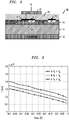
- FIG. 4 illustrates an exemplary silicon-based photodetector 30 formed in accordance with the present invention that addresses these limitations of the Patel et al. device.
- the elements that correspond to the prior art Patel et al. structure carry the same reference numerals.
- photodetector 30 further comprises a field plate 32 disposed above and separated from silicide strip 18.
- a dielectric region 34 separates field plate 32 from silicide strip 18.
- field plate 32 is easily incorporated into the standard CMOS process used for the fabrication of opto-electronic devices, where field plate 32 can be incorporated into the processing steps associated with the fabrication of the standard "metal 1" or "metal 2" layers.
- silicide strip 18 may itself be fabricated during a conventional set of process steps without the need to "modify” the process to create an ultra-thin silicide strip. This additional realization further simplifies the overall device fabrication process.
- a voltage V F is applied to field plate 32, which will induce an electric field across silicide strip 18.
- the presence of the electric field will, as discussed above, influence the direction of the momentum of the "hot” electrons and allow for a greater number of "hot” electrons to escape over the Schottky barrier and increase the generated photocurrent.
- the applied field across silicide strip 18 will preferentially shift the direction of momentum of these "hot” electrons in the direction normal to the silicon-silicide interface, the desired direction for movement of the carries over the barrier.
- the vertical separation S between field plate 32 and silicide strip 18 influences the responsivity of the device.
- field plate 32 if field plate 32 is positioned too close to the waveguiding structure, it will absorb a portion of the propagating signal, reducing the sensitivity of photodetector 30.
- a preferred metal layer to be used as field plate 32 is the "metal 1" layer of a standard CMOS process; however, a "metal 2" layer can also be used.
- the spacing between silicide strip 18 and field plate 32 is preferably on the order of 0.2 - 2.0 ⁇ m, with a preferred minimum spacing on the order of about 0.4 ⁇ m.
- FIG. 5 is a graph of the generated photocurrent as a function of bias voltage (V C -V A ) for three different values of V F .
- V F V A
- V F V A
- V F V A
- V F >V A V A
- Plot B is associated with the prior art arrangement, where the voltage applied to field plate 32 does not create an electric field along silicide strip 18.
- V F voltage present at anode 24 (the contact to SOI layer 16)
- the created electric field along silicide strip 18 will "add” to the existing field and thus adjust the moment of additional "hot” electrons to be in a direction essentially normal to the material interface. These additional "hot” electrons will then escape over the Schottky barrier and add to the created photocurrent.
- V F voltage to field plate 32 that actually subtracts from the nominal value and reduces the responsivity of photodetector 30. Decreasing the responsivity may be desired in situations where there is a need to "match" the responsivity to other system components.
- the responsivity of the photodetector of the present invention may be performed initially upon fabrication to provide a desired responsivity value, or may exist in the finished device as a 'tunable' element that is capable of being adjusted over time in various installations.
Description
- The present invention relates to a silicon-based Schottky barrier infrared (IR) optical detector and, more particularly, to a planar, waveguide-based IR optical detector including an additional field plate to improve the responsivity of the detector.
- Semiconductor devices using metal-semiconductor barriers (referred to as Schottky barriers) instead of p-n junctions have been developed to convert incident light into electrical energy. Silicon is often used as the semiconductor material in Schottky barrier photodetectors operating in the IR portion of the electromagnetic energy spectrum. In its most conventional form, a silicon-based Schottky barrier photodiode consists of a thin metallic film (such as a silicide film) disposed on a silicon layer. Incident light is applied perpendicular to (i.e., "normal to") this structure, passing through the relatively thin metallic film, where the thin film absorbs only a portion of the light, thus resulting in extremely low external quantum efficiency levels. As a result, conventional "normal incidence" photodetectors require a relatively large active detection area in order to collect a sufficient amount of optical energy to function properly. However, as the detection area increases, the dark current (unwanted noise signal) increases as well. Moreover, while relatively simple in structure, such normal incidence detectors typically require cooling, again associated with a relatively high dark current value.
- Improvements in optical absorption and quantum efficiency in silicon-based Schottky barrier photodetectors have been the source of much investigation over the years. In one case, the optical absorption has been improved by inducing a surface plasmon mode at the metal-semiconductor interface, as disclosed in
U.S. Pat. No. 5,685,919 issued to K. Saito et al. on Nov. 11, 1997 . In this arrangement, a semicylindrical lens is disposed over the metallic layer and used to re-orient the incoming light from normal incidence to an angle associated with creating the surface plasmon layer.U.S. Pat. No. 4,857,973, issued to A. C. Yang et al. on Aug. 15, 1989 discloses an alternative Schottky barrier photodetector arrangement, where the photodetector is monolithically integrated with a single crystal silicon rib waveguide and positioned to absorb the "tail" of the optical signal as it passes along the rib waveguide underneath a silicide layer. While an improvement in absorption efficiency may be achieved with the Yang et al. structure, significant losses remain in terms of scattering losses along the sidewalls of the rib waveguide structure inasmuch as the rib is created by partially removing portions of a relatively thick silicon layer. Moreover, significant difficulties remain in terms of controlling the dimensions (particularly the height), as well as the smoothness, of such a rib waveguide structure. Indeed, the implementation of a "rib" structure (particularly with sub-micron dimensions) is extremely difficult with CMOS-based conventional processing technologies. Further, the non-planar geometry of the Yang et al. structure is not considered as a preferred arrangement from a manufacturing point of view, particularly in terms of the reliability and robustness of the design. - An exemplary prior art silicon-based photodetector that is compatible with conventional CMOS processing is described in
US Patent 7,358,585, issued to V. Patel et al. on April 15, 2008 and assigned to the assignee of this application. In the Patel et al. structure, a silicide layer (or other appropriate metallic layer) is disposed over a planar silicon waveguide layer formed as a sub-micron thick surface layer of a "silicon-on-insulator" (SOI) structure (this sub-micron surface waveguide layer often referred to in the art as the "SOI layer"). Ohmic contacts are applied to both the planar SOI layer of the SOI structure and the silicide layer. An optical signal propagating laterally along the optical waveguide within the planar SOI layer will thus pass under the silicide layer, where the "tail" of the optical energy will intercept the silicide and be converted into electrical energy. Since the arrangement of Patel et al. is based on implementing a silicide detector on a planar silicon surface and does not require the formation of a single crystal silicon rib waveguide, significant improvements in efficiency over the structure of Yang et al. can be realized, while also being compatible with conventional planar CMOS processing technologies. - While considered to be an advance over existing devices, the planar, waveguide-based structure of Patel et al. has been found to be somewhat limited in its responsivity, associated with the inherent properties of the silicide material itself. Inasmuch as silicide detectors were initially designed for use in power monitoring applications, responsivity and processing simplicity were not the concerns that they are today.
- Thus, a need remains for a high speed silicon-based detector that remains compatible with standard CMOS processing, yet provides the responsivity required for use as a power monitor or feedback detector in high speed systems.
- The need remaining in the prior art is addressed by the present invention, which relates to a silicon-based Schottky barrier infrared (IR) optical detector and, more particularly, to a planar, waveguide-based IR optical detector including an additional field plate to improve the responsivity of the detector.
- The present invention is a silicon-based infrared photodetector as defined in
Claim 1 of the appended claims. Details of certain embodiments are set out in the dependent claims. - In accordance with the present invention, a separate conductive region (i.e., "field plate") is disposed over, and separated from the silicide layer forming the detector itself. Preferably, a conventional metal layer being used for other purposes (for example, the first layer of the standard metal conductor fabrication process) in a multi-layer metallization step in a CMOS fabrication process is used to create the field plate without needing to change any steps in the process. Moreover, it is preferred that the silicide layer used to form the detector itself is fabricated during the same processing step (i.e., defined as part of the same photolithography step) as other contact regions in the device.
- A voltage is applied to the field plate to create an electric field in the vicinity of the detector's silicide layer. By creating the electric field, the responsivity of the device may be "tuned" so as to adjust the direction and momentum of "hot" carriers (electrons or holes, depending on the conductivity of the silicon) with respect to the Schottky barrier/silicon layer interface. The applied electric field functions to change the direction of movement of the "hot" carriers to align with the preferred direction "normal" to the silicon-silicide interface, allowing for an increased number of carriers to move over the Schottky barrier and add to the generated photocurrent. That is, the inclusion of a biased field plate provides the directional influence required to adjust the direction of the "hot" carriers so as to assist in their injection over the Schottky barrier.
- In one embodiment, the actual voltage applied to the field plate is adjusted to modify the directional influence applied to the momentum of the carriers, where the adjustments may also be such that an "opposite" directional influence is applied (which decreases the generated photocurrent). The ability to "tune" the responsivity with an applied voltage is useful in matching the performance of the photodetector to other components in the system.
- It has also been discovered that the thickness of the silicide used to form the photodetector plays a relatively small role in device performance, where a silicide layer of thickness up to 500Å can be used within significant degradation in performance. Thus, it is been found that the detector silicide can be formed during the conventional fabrication process used to form other silicide regions (such as contact regions) and may have the same thickness and microstructure as these other silicide regions and still provide adequate performance as a power monitor detector. This approach is considered to significantly reduce the overall processing complexity of the detector fabrication process, since the same photolithography step and processing steps are used to form the detector silicide layer and the other contact regions.
- Other and further embodiments and features of the present invention will become apparent during the course of the following discussion and by reference to the accompanying drawings.
- Referring now to the drawings, where like numerals represent like parts in several views:
-
FIG. 1 is a band diagram associated with the operation of a prior art, normal incidence, Schottky barrier photodetector; -
FIG. 2 is a cut-away side view of an exemplary prior art SOI-based silicon photodetector; -
FIG. 3 is a diagram of the solid angle associated with the escape of hot electrons in moment space; -
FIG. 4 is a cut-away side view of an exemplary SOI-based Schottky barrier photodetector of the present invention, incorporating a field plate over the silicide layer; -
FIG. 5 is a plot of the change in responsivity of the inventive detector, illustrating the ability to "tune" the responsivity as a function of voltage applied to the field plate. - As described above, the present invention is directed to a silicon-based Schottky barrier detector including an additional electrode (i.e., "field plate") to apply an electric field across the silicide region of the detector so as to increase the movement of "hot" carriers (either electrons or holes, depending on the conductivity of the silicon; hereinafter described primarily as "hot" electrons) over the Schottky barrier and improve the responsivity of the device. The presence of the electric field will preferentially direct "hot" electrons in the manner required to cross the Schottky barrier (i.e., in a direction normal to the silicide-silicon interface) and thus increase the number of carriers that actually cross the barrier and contribute to the photocurrent. Advantageously, the fabrication process and materials of the inventive detector remain compatible with conventional, planar CMOS process technology associated with the semiconductor industry.
- In accordance with the present invention, a Schottky barrier junction is formed on the sub-micron thick, planar silicon waveguiding surface layer ("SOI layer") of an SOI structure. This Schottky barrier junction is formed in such a way that the optical signal propagating laterally along a waveguide within the planar SOI layer (traveling in the direction parallel to the junction) is continuously absorbed into the overlying silicide layer as it passes thereunder. As a result of this geometry, even a relatively thin silicide layer (e.g., a few monolayers thick) will absorb a large portion of the signal over a distance of a few microns.
- The field plate layer (preferably fabricated as a metal region of a conventional CMOS multi-layer metallization layer) is positioned above the detector silicide layer and is controlled by an applied voltage to create an electric field across the detector silicide layer. Creating this electric field has been found to modify the direction of the "hot" electrons, resulting in a higher or lower (depending upon the polarity of the applied field) number of "hot" electrons crossing the Schottky barrier and generating a larger (or smaller) photocurrent or responsivity. As will be described in detail below, the responsivity of the detector can be increased or decreased (in general, "tuned"), depending on the polarity of the voltage applied to the field plate layer with respect to the voltage potential between the anode and cathode terminals of the photodetector itself.
- The basic operation of a conventional, prior art "normal incidence" Schottky-barrier infrared photodetector is first described so as to form a basis for distinguishing the subject matter of the present invention. Referring to
FIG. 1 , an energy band diagram is illustrated to describe the operation of such a conventional Schottky-barrier photodetector. The incoming infrared radiation is incident in a normal incidence manner on a silicide layer and results in the excitation of a photocurrent across the Schottky barrier (defined as having a barrier height φms) by internal photoemission into an underlying silicon layer. In the arrangement ofFIG. 1 , it is presumed that the silicon layer comprises an n-type silicon material. Since silicon itself is transparent to 1R radiation with a photon energy less than the band gap of silicon (1.12 eV), the silicon layer does not contribute to the photocurrent by absorption of infrared photons (through the creation of electron-hole pairs). Particularly, the infrared photons are absorbed into the silicide layer by transferring their energy and momentum to the free carriers. Indeed, the "hot" electrons (or "hot" holes when using a p-type layer) that have sufficient energy, as well as the requisite directional properties, will go over the Schottky barrier and be injected into the silicon layer, leaving a net positive (negative) charge on the silicide electrode. - In order to improve the performance of the Schottky barrier IR detector to detect radiation in the 1.10-1.65 µm band of interest for optical communications, the previously-cited Patel et al. arrangement proposed the use of a lateral incidence photodetector in place of the conventional normal incidence photodetector structure, the lateral incidence photodetector formed as an integral part of an SOI structure including a sub-micron surface layer waveguide.
-
FIG. 2 contains a side view of an exemplary Schottky barrierIR photodetector arrangement 10 formed in accordance with the Patel et al. design.Photodetector 10 comprises a conventional "silicon-on-insulator" (SOI) structure, including asilicon substrate 12, insulator layer 14 (usually of SiO2) and a planar silicon surface layer 16 (also referred to as SOI layer 16), whereSOI layer 16 is preferably formed to have a thickness of less than one micron and is used to support the propagation of an optical mode therealong, as shown inFIG. 2 . It is to be understood thatSOI layer 16 may comprise either a planar single crystal silicon or a planar crystalline silicon (or Si-Ge) layer that has been processed to be in a "strained" lattice state (the strained silicon layer exhibiting a higher mobility rate for the carriers by reducing the mean free path length L). - In order to form the metal-semiconductor interface required for a Schottky barrier, a
silicide strip 18 is disposed along a portion oftop surface 20 ofplanar SOI layer 16. In practice, any one of the silicides that forms an appropriate Schottky barrier for the wavelength to be detected may be used in the formation of this structure, since the ability to form a silicide on a silicon surface is generally understood in the planar CMOS processing industry. Accordingly, silicides based on cobalt, nickel, molybdenum, tantalum, tungsten and titanium are the most desired silicide layers for telecommunications application (and are also compatible with CMOS processes). -
Silicide strip 18 may be formed as a single crystal (which is possible with some silicides), or as a polycrystalline material. For a polycrystalline silicide strip, scattering from grain boundaries plays a role (in association with the strip thickness) in determination of the "gain" factor of the detector. In this case, the processing conditions can be controlled, using well-known means, to optimize the grain formation in the silicide. - A first
electrical contact 22 is made to silicidestrip 18 so as to form a first electrode ofphotodetector 10. A secondelectrical contact 24 is made directly toplanar SOI layer 16 along itstop surface 20, where first andsecond contacts FIG. 2 . Thus, as an optical beam propagates alongplanar SOI layer 16, the "hot" electrons injected from silicide strip I8 will result in the generation of a photocurrent between firstelectrical contact 22 and secondelectrical contact 24, where a measurement of this photocurrent can then be used as an indication of the optical power of the propagating lightwave signal. - As a result of utilizing this waveguide-based structure for the IR photodetector, it is possible to implement a device that is capable of operating at (or even above) room temperature (which is problematic with the prior art normal incidence detectors). Responsivity in general is a measure of quantum efficiency of the device measured by determining the ratio of generated photocurrent to incoming optical power. More particularly, responsivity R can be defined by the following relation:

- This limitation can be understood with reference to
FIG. 3 , which is a depiction of the solid angle required for the escape of "hot" electrons into momentum space. The quantities of energy and moment are both illustrated inFIG. 3 . While a large number of "hot" electrons are created in the first instance upon incidence of photons on the silicide, only a fraction of the "hot" electrons with energy greater than φms and momentum in a direction nearly normal (perpendicular) to the silicide-silicon interface can cross the Schottky barrier. The diagram inFIG. 3 illustrates vectors associated with both the energy E 1/2 andmomentum 
- The responsivity of a photodetector, when defined as the ratio of generated photocurrents/input optical signal power, is clearly associated with the number of hot electrons meeting this "nearly normal" angular directional criterion (defined by the quantity 2πr2(1-cos θ)), shown as the shaded region of
FIG. 3 . Merely increasing the energy imparted to these carriers is not sufficient to increase the generated photocurrent (and hence responsivity of the detector), unless the direction of momentum is also proper; that is, along a direction nearly normal to the interface between the silicon and silicide. In accordance with the present invention, therefore, an external electric field is applied to the silicide region of the detector, using the field plate configuration, to influence the direction of momentum of the "hot" electrons. -
FIG. 4 illustrates an exemplary silicon-basedphotodetector 30 formed in accordance with the present invention that addresses these limitations of the Patel et al. device. The elements that correspond to the prior art Patel et al. structure carry the same reference numerals. As shown inFIG. 4 ,photodetector 30 further comprises afield plate 32 disposed above and separated fromsilicide strip 18. Adielectric region 34separates field plate 32 fromsilicide strip 18. Advantageously,field plate 32 is easily incorporated into the standard CMOS process used for the fabrication of opto-electronic devices, wherefield plate 32 can be incorporated into the processing steps associated with the fabrication of the standard "metal 1" or "metal 2" layers. Moreover, as mentioned above, it has been discovered thatsilicide strip 18 may itself be fabricated during a conventional set of process steps without the need to "modify" the process to create an ultra-thin silicide strip. This additional realization further simplifies the overall device fabrication process. - In accordance with the present invention, a voltage VF is applied to
field plate 32, which will induce an electric field acrosssilicide strip 18. The presence of the electric field will, as discussed above, influence the direction of the momentum of the "hot" electrons and allow for a greater number of "hot" electrons to escape over the Schottky barrier and increase the generated photocurrent. The applied field acrosssilicide strip 18 will preferentially shift the direction of momentum of these "hot" electrons in the direction normal to the silicon-silicide interface, the desired direction for movement of the carries over the barrier. - It is to be noted that the vertical separation S between
field plate 32 andsilicide strip 18 influences the responsivity of the device. In particular, thecloser field plate 32 is to silicidestrip 18, the less applied voltage is needed to create the same strength electric field. However, iffield plate 32 is positioned too close to the waveguiding structure, it will absorb a portion of the propagating signal, reducing the sensitivity ofphotodetector 30. As mentioned above, a preferred metal layer to be used asfield plate 32 is the "metal 1" layer of a standard CMOS process; however, a "metal 2" layer can also be used. The spacing betweensilicide strip 18 andfield plate 32 is preferably on the order of 0.2 - 2.0 µm, with a preferred minimum spacing on the order of about 0.4 µm. -
FIG. 5 is a graph of the generated photocurrent as a function of bias voltage (VC-VA) for three different values of VF. In plot A, VF < VA; in plot B, VF = VA; and in plot C, VF>VA. Plot B is associated with the prior art arrangement, where the voltage applied to fieldplate 32 does not create an electric field alongsilicide strip 18. Referring to plot A, if voltage VF is selected to be less than the voltage present at anode 24 (the contact to SOI layer 16), the created electric field alongsilicide strip 18 will "add" to the existing field and thus adjust the moment of additional "hot" electrons to be in a direction essentially normal to the material interface. These additional "hot" electrons will then escape over the Schottky barrier and add to the created photocurrent. - As shown in
FIG. 5 , by adjusting the value of VF, it is possible to "tune" the influence of the applied electric field on the movement of "hot" electrons over the barrier. In fact, it is possible to apply a voltage to fieldplate 32 that actually subtracts from the nominal value and reduces the responsivity ofphotodetector 30. Decreasing the responsivity may be desired in situations where there is a need to "match" the responsivity to other system components. - In general, by virtue of the application of a tunable voltage to field
plate 32, it is possible to tune the responsivity of the photodetector of the present invention. The tuning may be performed initially upon fabrication to provide a desired responsivity value, or may exist in the finished device as a 'tunable' element that is capable of being adjusted over time in various installations. - While the inventive photodetector has been described in an embodiment where "hot" electrons are the carriers responsible for the generation of the photocurrent, it is to be understood that "hot" holes may be the carriers creating the photocurrent in an arrangement where p-doped silicon is utilized (and the polarity of the voltage applied to the field plate adjusted accordingly).
- In light of all of the above, therefore, the present invention is intended to be limited only by the scope of the claims appended hereto.
Claims (12)
- A silicon-based infrared photodetector (30) integrated on a silicon-on-insulator, SOI, substrate (12, 14, 16) with an optical waveguide, the SOI substrate (12, 14, 16) including a planar SOI surface layer (16), the optical waveguide being formed by the planar SOI surface layer (16), the silicon-based infrared photodetector (30) comprising:a metallic strip (18) disposed over a portion of the planar SOI surface layer (16) along the direction of propagation of an optical signal along the optical waveguide, the metallic strip (18) forming a Schottky barrier with the optical waveguide, wherein the Schottky barrier is arranged such that, in use, an optical signal propagating laterally along the optical waveguide travels in a direction parallel to the Schottky barrier;a first ohmic contact (24) disposed on the planar SOI surface layer (16) at a first contact area; anda second ohmic contact (22) disposed on the metallic strip (18) at a second contact area;characterised in that the silicon-based infrared photodetector further comprises a field plate electrode (32) disposed over and separated from the metallic strip (18), wherein the application of a voltage to the field plate electrode (32) modifies the electric field along the metallic strip (18) to preferentially direct the momentum of hot carriers, influencing the number of hot carriers that cross over the Schottky barrier, which in turn modifies the photocurrent generated by the silicon-based infrared photodetector.
- A silicon-based infrared photodetector as defined in claim 1 where the polarity of the voltage applied to the field plate electrode (32) is controlled to preferentially direct the momentum of hot carriers in a direction nearly normal with respect to the interface between the planar SOI surface layer (16) and the metallic strip (18), increasing the number of hot carriers that cross over the Schottky barrier.
- A silicon-based infrared photodetector as defined in claim 1 wherein the voltage applied to the field plate electrode (32) is tunable to adjust the number of hot conductors that cross over the Schottky barrier and thereby adjust the sensitivity of the photodetector.
- A silicon-based infrared photodetector as defined in claim 1 wherein the metallic strip (18) comprises a layer of silicide material disposed during conventional CMOS processing.
- A silicon-based infrared photodetector as defined in claim 4 wherein the layer of silicide material (18) is processed as a single step with a silicide region used as a contact.
- A silicon-based infrared photodetector as defined in claim 1 wherein the field plate electrode (32) comprises a portion of a first conductor layer disposed during conventional CMOS processing.
- A silicon-based infrared photodetector as defined in claim 1 wherein the field plate electrode (32) comprises a portion of a second conductor layer disposed during conventional CMOS processing.
- A silicon-based infrared photodetector as defined in claim 1 wherein the planar SOI surface layer (16) is n-doped and the hot carriers comprise hot electrons.
- A silicon-based infrared photodetector as defined in claim 1 wherein the planar SOI surface layer (16) is p-doped and the hot carriers comprise hot holes.
- A silicon-based infrared photodetector as defined in claim 1 wherein the field plate electrode (32) is separated from the metallic strip (18) by a distance of no greater than 2 µm.
- A silicon-based infrared photodetector as defined in claim 1 wherein the field plate electrode (32) is separated from the metallic strip (18) by a distance of no less than 0.2 µm.
- A silicon-based infrared photodetector as defined in claim 1 wherein the field plate electrode (32) is separated from the metallic strip (18) by a distance of 0.4 µm.
Applications Claiming Priority (3)
| Application Number | Priority Date | Filing Date | Title |
|---|---|---|---|
| US33985510P | 2010-03-10 | 2010-03-10 | |
| US13/038,470 US8618625B2 (en) | 2010-03-10 | 2011-03-02 | Silicon-based schottky barrier detector with improved responsivity |
| PCT/US2011/026940 WO2011112406A2 (en) | 2010-03-10 | 2011-03-03 | Silicon-based schottky barrier detector with improved responsivity |
Publications (3)
| Publication Number | Publication Date |
|---|---|
| EP2545593A2 EP2545593A2 (en) | 2013-01-16 |
| EP2545593A4 EP2545593A4 (en) | 2017-12-27 |
| EP2545593B1 true EP2545593B1 (en) | 2018-12-12 |
Family
ID=44559154
Family Applications (1)
| Application Number | Title | Priority Date | Filing Date |
|---|---|---|---|
| EP11753819.9A Active EP2545593B1 (en) | 2010-03-10 | 2011-03-03 | Silicon-based schottky barrier detector with improved responsivity |
Country Status (4)
| Country | Link |
|---|---|
| US (1) | US8618625B2 (en) |
| EP (1) | EP2545593B1 (en) |
| CN (1) | CN102782880B (en) |
| WO (1) | WO2011112406A2 (en) |
Families Citing this family (11)
| Publication number | Priority date | Publication date | Assignee | Title |
|---|---|---|---|---|
| CN102561295B (en) * | 2012-01-09 | 2014-06-11 | 长沙理工大学 | Method for observing and calculating depth of newly-generated swelling shrinking deformation of excavation expansive soil slope surface |
| TWI493739B (en) * | 2013-06-05 | 2015-07-21 | Univ Nat Taiwan | Hot-carrier photo-electric conversion apparatus and method thereof |
| JP6228874B2 (en) * | 2014-03-19 | 2017-11-08 | 株式会社日立製作所 | Semiconductor optical device |
| EP3096180A1 (en) * | 2015-05-20 | 2016-11-23 | Philipps-Universität Marburg | Method for expanding the frequency spectrum of an electromagnetic wave and component for realizing the same |
| US9660117B1 (en) | 2016-09-19 | 2017-05-23 | Sharp Kabushiki Kaisha | Energy selective photodetector |
| CN106252454B (en) | 2016-09-26 | 2017-08-25 | 京东方科技集团股份有限公司 | A kind of photodetector and Electro-Optical Sensor Set |
| CN110164981B (en) * | 2018-05-16 | 2022-04-29 | 北京纳米能源与系统研究所 | Method for adjusting Schottky barrier of Schottky device |
| CN110143563B (en) * | 2018-05-16 | 2021-12-24 | 北京纳米能源与系统研究所 | Schottky sensor system |
| CN109727849B (en) * | 2018-12-17 | 2020-11-06 | 浙江大学 | Method for instantaneously improving responsivity of carrier depletion type silicon optical power monitor based on defect state mechanism without crosstalk |
| CN111947792B (en) * | 2020-08-26 | 2022-10-11 | 合肥工业大学 | Color detection system based on palladium diselenide/ultrathin silicon/palladium diselenide Schottky junction and preparation method thereof |
| CN112563345B (en) * | 2020-12-09 | 2023-04-28 | 西安交通大学 | Outer conductor electrode structure for homogenizing plane type photoconductive switch electric field, photoconductive switch device and method |
Family Cites Families (12)
| Publication number | Priority date | Publication date | Assignee | Title |
|---|---|---|---|---|
| JP2666889B2 (en) | 1995-03-27 | 1997-10-22 | 工業技術院長 | Photoelectric conversion method and photoelectric conversion element |
| US6211560B1 (en) * | 1995-06-16 | 2001-04-03 | The United States Of America As Represented By The Secretary Of The Air Force | Voltage tunable schottky diode photoemissive infrared detector |
| EP0993053A1 (en) | 1998-10-09 | 2000-04-12 | STMicroelectronics S.r.l. | Infrared detector integrated with a waveguide and method of manufacturing |
| JP2000164918A (en) * | 1998-11-27 | 2000-06-16 | Mitsubishi Electric Corp | Schottky junction semiconductor photodetector |
| JP3684149B2 (en) | 2000-11-15 | 2005-08-17 | 三菱電機株式会社 | Thermal infrared detector |
| CA2365499C (en) * | 2000-12-26 | 2011-02-15 | National Research Council Of Canada | High speed and high efficiency si-based photodetectors using waveguides formed with silicides for near ir applications |
| CA2514256A1 (en) * | 2003-03-04 | 2004-09-16 | Spectalis Corp. | Schottky barrier photodetectors |
| KR20060130045A (en) * | 2003-11-20 | 2006-12-18 | 시옵티컬 인코포레이티드 | Silicon-based schottky barrier infrared optical detector |
| WO2006066611A1 (en) * | 2004-12-24 | 2006-06-29 | Pirelli & C. S.P.A. | Photodetector in germanium on silicon |
| JP2008051522A (en) | 2006-08-22 | 2008-03-06 | Nec Tokin Corp | Thermal type infrared detector and manufacturing method therefor |
| JP4975669B2 (en) | 2008-03-25 | 2012-07-11 | 株式会社東芝 | Infrared detector and solid-state imaging device equipped with the infrared detector |
| JP5264597B2 (en) * | 2008-04-03 | 2013-08-14 | 三菱電機株式会社 | Infrared detector and infrared solid-state imaging device |
-
2011
- 2011-03-02 US US13/038,470 patent/US8618625B2/en active Active
- 2011-03-03 CN CN201180012674.8A patent/CN102782880B/en not_active Expired - Fee Related
- 2011-03-03 WO PCT/US2011/026940 patent/WO2011112406A2/en active Application Filing
- 2011-03-03 EP EP11753819.9A patent/EP2545593B1/en active Active
Non-Patent Citations (1)
| Title |
|---|
| None * |
Also Published As
| Publication number | Publication date |
|---|---|
| WO2011112406A3 (en) | 2011-12-08 |
| WO2011112406A2 (en) | 2011-09-15 |
| EP2545593A2 (en) | 2013-01-16 |
| CN102782880B (en) | 2015-09-23 |
| US20110221019A1 (en) | 2011-09-15 |
| CN102782880A (en) | 2012-11-14 |
| EP2545593A4 (en) | 2017-12-27 |
| US8618625B2 (en) | 2013-12-31 |
Similar Documents
| Publication | Publication Date | Title |
|---|---|---|
| EP2545593B1 (en) | Silicon-based schottky barrier detector with improved responsivity | |
| EP1716596B1 (en) | Silicon-based schottky barrier infrared optical detector | |
| US7256470B2 (en) | Photodiode with controlled current leakage | |
| US8618622B2 (en) | Photodetector optimized by metal texturing provided on the rear surface | |
| US11682741B2 (en) | Electromagnetic wave detector | |
| EP0651448B1 (en) | Improved metal-semiconductor-metal photodetector | |
| US20080105940A1 (en) | SOI-based inverse nanotaper optical detector | |
| EP2022094A1 (en) | Detecting plasmons using a metallurgical junction | |
| JPH0469825B2 (en) | ||
| US10128386B2 (en) | Semiconductor structure comprising an absorbing area placed in a focusing cavity | |
| EP3480861B1 (en) | Light-receiving element and near infrared light detector | |
| US9165967B2 (en) | Semiconductor structure able to receive electromagnetic radiation, semiconductor component and process for fabricating such a semiconductor structure | |
| US5969375A (en) | Infrared detector with non-cooled quantum well structure | |
| US4740823A (en) | Photo-detectors | |
| US8410420B1 (en) | Semiconductor travelling-wave evanescent waveguide photodetector | |
| WO2009071916A1 (en) | Infrared avalanche photodiode structure with low excess noise and its manufacturing method | |
| US4586067A (en) | Photodetector with isolated avalanche region | |
| EP3480862A1 (en) | Light-receiving element and near infrared light detector | |
| JPS60247979A (en) | Semiconductor optical element | |
| JPH11330536A (en) | Semiconductor light receiving element | |
| Zhang et al. | GeSn on Si avalanche photodiodes for short wave infrared detection | |
| Sednev et al. | Current–Voltage Characteristics of nBp Structures with Absorbing In 0.53 Ga 0.47 As Layer | |
| US20230253516A1 (en) | Photodetector | |
| CN114400266B (en) | Photoelectric detector integrated with double absorption areas and preparation method thereof | |
| EP2224497A1 (en) | Photodetector relying on phonon detection |
Legal Events
| Date | Code | Title | Description |
|---|---|---|---|
| PUAI | Public reference made under article 153(3) epc to a published international application that has entered the european phase |
Free format text: ORIGINAL CODE: 0009012 |
|
| 17P | Request for examination filed |
Effective date: 20121010 |
|
| AK | Designated contracting states |
Kind code of ref document: A2 Designated state(s): AL AT BE BG CH CY CZ DE DK EE ES FI FR GB GR HR HU IE IS IT LI LT LU LV MC MK MT NL NO PL PT RO RS SE SI SK SM TR |
|
| DAX | Request for extension of the european patent (deleted) | ||
| RAP1 | Party data changed (applicant data changed or rights of an application transferred) |
Owner name: CISCO TECHNOLOGY, INC. |
|
| A4 | Supplementary search report drawn up and despatched |
Effective date: 20171127 |
|
| RIC1 | Information provided on ipc code assigned before grant |
Ipc: H01L 31/108 20060101AFI20171121BHEP Ipc: H01L 31/09 20060101ALI20171121BHEP |
|
| GRAP | Despatch of communication of intention to grant a patent |
Free format text: ORIGINAL CODE: EPIDOSNIGR1 |
|
| STAA | Information on the status of an ep patent application or granted ep patent |
Free format text: STATUS: GRANT OF PATENT IS INTENDED |
|
| INTG | Intention to grant announced |
Effective date: 20180703 |
|
| GRAS | Grant fee paid |
Free format text: ORIGINAL CODE: EPIDOSNIGR3 |
|
| GRAA | (expected) grant |
Free format text: ORIGINAL CODE: 0009210 |
|
| STAA | Information on the status of an ep patent application or granted ep patent |
Free format text: STATUS: THE PATENT HAS BEEN GRANTED |
|
| AK | Designated contracting states |
Kind code of ref document: B1 Designated state(s): AL AT BE BG CH CY CZ DE DK EE ES FI FR GB GR HR HU IE IS IT LI LT LU LV MC MK MT NL NO PL PT RO RS SE SI SK SM TR |
|
| REG | Reference to a national code |
Ref country code: GB Ref legal event code: FG4D |
|
| REG | Reference to a national code |
Ref country code: CH Ref legal event code: EP |
|
| REG | Reference to a national code |
Ref country code: AT Ref legal event code: REF Ref document number: 1077132 Country of ref document: AT Kind code of ref document: T Effective date: 20181215 |
|
| REG | Reference to a national code |
Ref country code: DE Ref legal event code: R096 Ref document number: 602011054749 Country of ref document: DE |
|
| REG | Reference to a national code |
Ref country code: IE Ref legal event code: FG4D |
|
| REG | Reference to a national code |
Ref country code: NL Ref legal event code: MP Effective date: 20181212 |
|
| REG | Reference to a national code |
Ref country code: LT Ref legal event code: MG4D |
|
| PG25 | Lapsed in a contracting state [announced via postgrant information from national office to epo] |
Ref country code: ES Free format text: LAPSE BECAUSE OF FAILURE TO SUBMIT A TRANSLATION OF THE DESCRIPTION OR TO PAY THE FEE WITHIN THE PRESCRIBED TIME-LIMIT Effective date: 20181212 Ref country code: NO Free format text: LAPSE BECAUSE OF FAILURE TO SUBMIT A TRANSLATION OF THE DESCRIPTION OR TO PAY THE FEE WITHIN THE PRESCRIBED TIME-LIMIT Effective date: 20190312 Ref country code: HR Free format text: LAPSE BECAUSE OF FAILURE TO SUBMIT A TRANSLATION OF THE DESCRIPTION OR TO PAY THE FEE WITHIN THE PRESCRIBED TIME-LIMIT Effective date: 20181212 Ref country code: LT Free format text: LAPSE BECAUSE OF FAILURE TO SUBMIT A TRANSLATION OF THE DESCRIPTION OR TO PAY THE FEE WITHIN THE PRESCRIBED TIME-LIMIT Effective date: 20181212 Ref country code: BG Free format text: LAPSE BECAUSE OF FAILURE TO SUBMIT A TRANSLATION OF THE DESCRIPTION OR TO PAY THE FEE WITHIN THE PRESCRIBED TIME-LIMIT Effective date: 20190312 Ref country code: FI Free format text: LAPSE BECAUSE OF FAILURE TO SUBMIT A TRANSLATION OF THE DESCRIPTION OR TO PAY THE FEE WITHIN THE PRESCRIBED TIME-LIMIT Effective date: 20181212 Ref country code: LV Free format text: LAPSE BECAUSE OF FAILURE TO SUBMIT A TRANSLATION OF THE DESCRIPTION OR TO PAY THE FEE WITHIN THE PRESCRIBED TIME-LIMIT Effective date: 20181212 |
|
| REG | Reference to a national code |
Ref country code: AT Ref legal event code: MK05 Ref document number: 1077132 Country of ref document: AT Kind code of ref document: T Effective date: 20181212 |
|
| PG25 | Lapsed in a contracting state [announced via postgrant information from national office to epo] |
Ref country code: AL Free format text: LAPSE BECAUSE OF FAILURE TO SUBMIT A TRANSLATION OF THE DESCRIPTION OR TO PAY THE FEE WITHIN THE PRESCRIBED TIME-LIMIT Effective date: 20181212 Ref country code: SE Free format text: LAPSE BECAUSE OF FAILURE TO SUBMIT A TRANSLATION OF THE DESCRIPTION OR TO PAY THE FEE WITHIN THE PRESCRIBED TIME-LIMIT Effective date: 20181212 Ref country code: RS Free format text: LAPSE BECAUSE OF FAILURE TO SUBMIT A TRANSLATION OF THE DESCRIPTION OR TO PAY THE FEE WITHIN THE PRESCRIBED TIME-LIMIT Effective date: 20181212 Ref country code: GR Free format text: LAPSE BECAUSE OF FAILURE TO SUBMIT A TRANSLATION OF THE DESCRIPTION OR TO PAY THE FEE WITHIN THE PRESCRIBED TIME-LIMIT Effective date: 20190313 |
|
| PG25 | Lapsed in a contracting state [announced via postgrant information from national office to epo] |
Ref country code: NL Free format text: LAPSE BECAUSE OF FAILURE TO SUBMIT A TRANSLATION OF THE DESCRIPTION OR TO PAY THE FEE WITHIN THE PRESCRIBED TIME-LIMIT Effective date: 20181212 |
|
| PG25 | Lapsed in a contracting state [announced via postgrant information from national office to epo] |
Ref country code: CZ Free format text: LAPSE BECAUSE OF FAILURE TO SUBMIT A TRANSLATION OF THE DESCRIPTION OR TO PAY THE FEE WITHIN THE PRESCRIBED TIME-LIMIT Effective date: 20181212 Ref country code: IT Free format text: LAPSE BECAUSE OF FAILURE TO SUBMIT A TRANSLATION OF THE DESCRIPTION OR TO PAY THE FEE WITHIN THE PRESCRIBED TIME-LIMIT Effective date: 20181212 Ref country code: PL Free format text: LAPSE BECAUSE OF FAILURE TO SUBMIT A TRANSLATION OF THE DESCRIPTION OR TO PAY THE FEE WITHIN THE PRESCRIBED TIME-LIMIT Effective date: 20181212 Ref country code: PT Free format text: LAPSE BECAUSE OF FAILURE TO SUBMIT A TRANSLATION OF THE DESCRIPTION OR TO PAY THE FEE WITHIN THE PRESCRIBED TIME-LIMIT Effective date: 20190412 |
|
| PG25 | Lapsed in a contracting state [announced via postgrant information from national office to epo] |
Ref country code: EE Free format text: LAPSE BECAUSE OF FAILURE TO SUBMIT A TRANSLATION OF THE DESCRIPTION OR TO PAY THE FEE WITHIN THE PRESCRIBED TIME-LIMIT Effective date: 20181212 Ref country code: SM Free format text: LAPSE BECAUSE OF FAILURE TO SUBMIT A TRANSLATION OF THE DESCRIPTION OR TO PAY THE FEE WITHIN THE PRESCRIBED TIME-LIMIT Effective date: 20181212 Ref country code: IS Free format text: LAPSE BECAUSE OF FAILURE TO SUBMIT A TRANSLATION OF THE DESCRIPTION OR TO PAY THE FEE WITHIN THE PRESCRIBED TIME-LIMIT Effective date: 20190412 Ref country code: RO Free format text: LAPSE BECAUSE OF FAILURE TO SUBMIT A TRANSLATION OF THE DESCRIPTION OR TO PAY THE FEE WITHIN THE PRESCRIBED TIME-LIMIT Effective date: 20181212 Ref country code: SK Free format text: LAPSE BECAUSE OF FAILURE TO SUBMIT A TRANSLATION OF THE DESCRIPTION OR TO PAY THE FEE WITHIN THE PRESCRIBED TIME-LIMIT Effective date: 20181212 |
|
| REG | Reference to a national code |
Ref country code: DE Ref legal event code: R097 Ref document number: 602011054749 Country of ref document: DE |
|
| PLBE | No opposition filed within time limit |
Free format text: ORIGINAL CODE: 0009261 |
|
| STAA | Information on the status of an ep patent application or granted ep patent |
Free format text: STATUS: NO OPPOSITION FILED WITHIN TIME LIMIT |
|
| PG25 | Lapsed in a contracting state [announced via postgrant information from national office to epo] |
Ref country code: AT Free format text: LAPSE BECAUSE OF FAILURE TO SUBMIT A TRANSLATION OF THE DESCRIPTION OR TO PAY THE FEE WITHIN THE PRESCRIBED TIME-LIMIT Effective date: 20181212 Ref country code: DK Free format text: LAPSE BECAUSE OF FAILURE TO SUBMIT A TRANSLATION OF THE DESCRIPTION OR TO PAY THE FEE WITHIN THE PRESCRIBED TIME-LIMIT Effective date: 20181212 Ref country code: MC Free format text: LAPSE BECAUSE OF FAILURE TO SUBMIT A TRANSLATION OF THE DESCRIPTION OR TO PAY THE FEE WITHIN THE PRESCRIBED TIME-LIMIT Effective date: 20181212 Ref country code: SI Free format text: LAPSE BECAUSE OF FAILURE TO SUBMIT A TRANSLATION OF THE DESCRIPTION OR TO PAY THE FEE WITHIN THE PRESCRIBED TIME-LIMIT Effective date: 20181212 |
|
| REG | Reference to a national code |
Ref country code: CH Ref legal event code: PL |
|
| 26N | No opposition filed |
Effective date: 20190913 |
|
| PG25 | Lapsed in a contracting state [announced via postgrant information from national office to epo] |
Ref country code: LU Free format text: LAPSE BECAUSE OF NON-PAYMENT OF DUE FEES Effective date: 20190303 |
|
| REG | Reference to a national code |
Ref country code: BE Ref legal event code: MM Effective date: 20190331 |
|
| PG25 | Lapsed in a contracting state [announced via postgrant information from national office to epo] |
Ref country code: CH Free format text: LAPSE BECAUSE OF NON-PAYMENT OF DUE FEES Effective date: 20190331 Ref country code: IE Free format text: LAPSE BECAUSE OF NON-PAYMENT OF DUE FEES Effective date: 20190303 Ref country code: LI Free format text: LAPSE BECAUSE OF NON-PAYMENT OF DUE FEES Effective date: 20190331 |
|
| PG25 | Lapsed in a contracting state [announced via postgrant information from national office to epo] |
Ref country code: BE Free format text: LAPSE BECAUSE OF NON-PAYMENT OF DUE FEES Effective date: 20190331 |
|
| PG25 | Lapsed in a contracting state [announced via postgrant information from national office to epo] |
Ref country code: TR Free format text: LAPSE BECAUSE OF FAILURE TO SUBMIT A TRANSLATION OF THE DESCRIPTION OR TO PAY THE FEE WITHIN THE PRESCRIBED TIME-LIMIT Effective date: 20181212 |
|
| PG25 | Lapsed in a contracting state [announced via postgrant information from national office to epo] |
Ref country code: MT Free format text: LAPSE BECAUSE OF NON-PAYMENT OF DUE FEES Effective date: 20190303 |
|
| PG25 | Lapsed in a contracting state [announced via postgrant information from national office to epo] |
Ref country code: CY Free format text: LAPSE BECAUSE OF FAILURE TO SUBMIT A TRANSLATION OF THE DESCRIPTION OR TO PAY THE FEE WITHIN THE PRESCRIBED TIME-LIMIT Effective date: 20181212 |
|
| PG25 | Lapsed in a contracting state [announced via postgrant information from national office to epo] |
Ref country code: HU Free format text: LAPSE BECAUSE OF FAILURE TO SUBMIT A TRANSLATION OF THE DESCRIPTION OR TO PAY THE FEE WITHIN THE PRESCRIBED TIME-LIMIT; INVALID AB INITIO Effective date: 20110303 |
|
| PG25 | Lapsed in a contracting state [announced via postgrant information from national office to epo] |
Ref country code: MK Free format text: LAPSE BECAUSE OF FAILURE TO SUBMIT A TRANSLATION OF THE DESCRIPTION OR TO PAY THE FEE WITHIN THE PRESCRIBED TIME-LIMIT Effective date: 20181212 |
|
| PGFP | Annual fee paid to national office [announced via postgrant information from national office to epo] |
Ref country code: FR Payment date: 20230329 Year of fee payment: 13 |
|
| PGFP | Annual fee paid to national office [announced via postgrant information from national office to epo] |
Ref country code: GB Payment date: 20230328 Year of fee payment: 13 Ref country code: DE Payment date: 20230316 Year of fee payment: 13 |
|
| P01 | Opt-out of the competence of the unified patent court (upc) registered |
Effective date: 20230525 |