WO2024111494A1 - 薄板サーミスタおよび薄板サーミスタ搭載型圧電振動デバイス - Google Patents
薄板サーミスタおよび薄板サーミスタ搭載型圧電振動デバイス Download PDFInfo
- Publication number
- WO2024111494A1 WO2024111494A1 PCT/JP2023/041211 JP2023041211W WO2024111494A1 WO 2024111494 A1 WO2024111494 A1 WO 2024111494A1 JP 2023041211 W JP2023041211 W JP 2023041211W WO 2024111494 A1 WO2024111494 A1 WO 2024111494A1
- Authority
- WO
- WIPO (PCT)
- Prior art keywords
- thermistor
- thin plate
- plate
- electrode
- main surface
- Prior art date
- Legal status (The legal status is an assumption and is not a legal conclusion. Google has not performed a legal analysis and makes no representation as to the accuracy of the status listed.)
- Ceased
Links
Images


Classifications
-
- H—ELECTRICITY
- H01—ELECTRIC ELEMENTS
- H01C—RESISTORS
- H01C1/00—Details
- H01C1/14—Terminals or tapping points specially adapted for resistors; Arrangements of terminals or tapping points on resistors
- H01C1/142—Terminals or tapping points specially adapted for resistors; Arrangements of terminals or tapping points on resistors the terminals or tapping points being coated on the resistive element
-
- H—ELECTRICITY
- H01—ELECTRIC ELEMENTS
- H01C—RESISTORS
- H01C17/00—Apparatus or processes specially adapted for manufacturing resistors
- H01C17/06—Apparatus or processes specially adapted for manufacturing resistors adapted for coating resistive material on a base
- H01C17/065—Apparatus or processes specially adapted for manufacturing resistors adapted for coating resistive material on a base by thick film techniques, e.g. serigraphy
-
- H—ELECTRICITY
- H01—ELECTRIC ELEMENTS
- H01C—RESISTORS
- H01C7/00—Non-adjustable resistors formed as one or more layers or coatings; Non-adjustable resistors made from powdered conducting material or powdered semi-conducting material with or without insulating material
- H01C7/04—Non-adjustable resistors formed as one or more layers or coatings; Non-adjustable resistors made from powdered conducting material or powdered semi-conducting material with or without insulating material having negative temperature coefficient
-
- H—ELECTRICITY
- H03—ELECTRONIC CIRCUITRY
- H03H—IMPEDANCE NETWORKS, e.g. RESONANT CIRCUITS; RESONATORS
- H03H9/00—Networks comprising electromechanical or electro-acoustic elements; Electromechanical resonators
- H03H9/02—Details
Definitions
- the present invention relates to a thin plate thermistor used as a temperature sensor and a piezoelectric vibration device equipped with a thin plate thermistor.
- temperature-compensated frequency information can be obtained, enabling the operation of electronic devices to be maintained with high precision.
- Such a thermistor-equipped piezoelectric vibration device is configured such that a quartz crystal plate with an excitation electrode formed thereon is housed in a ceramic package, and a thermistor is attached to the outside of the plate to detect the environmental temperature surrounding the quartz crystal unit (see, for example, Patent Document 1).
- Thermistors have a laminated structure in which multiple layers of thermistor material and operating electrodes are stacked together, and those with a thickness of about 0.3 mm to 0.1 mm are commercially available and in use.
- Thermistors are required to detect the temperature environment surrounding the quartz crystal unit with a small time lag.
- the thermistors used to date have a laminated structure, which means that they require a certain thickness (height).
- the electrodes of laminated thermistors are made of thick film electrodes produced by screen printing, etc., making the structure unsuitable for making thin thermistors.
- thermistor instead of using a thermistor with a laminated structure in which multiple thermistor material layers and operating electrodes are stacked on top of each other, it is conceivable to use a thermistor with electrodes formed on the surface of a single thermistor plate; however, to date, no thermistor with electrodes formed on the surface of a single thermistor plate has been put to practical use. Such thermistors with electrodes formed on the surface of a single thermistor plate are prone to cracking and chipping at the ends.
- the present invention aims to provide a thin plate thermistor that is less likely to crack or chip at its ends, and a piezoelectric vibration device equipped with such a thin plate thermistor.
- a thin plate thermistor according to the present invention is a thin plate thermistor having a single thermistor plate and an electrode formed on one surface of the thermistor plate, characterized in that the surface roughness of either the one surface of the thermistor plate or the other surface opposite to the one surface is smaller at the ends than at the center.
- the surface roughness of one side of the thermistor plate is smaller at the end than at the center, making it less likely for cracks or chips to occur on one side of the end of the thermistor plate, and as a result, the mechanical strength of the thin plate thermistor can be improved.
- Another thin plate thermistor according to the present invention is a thin plate thermistor having a single thermistor plate and an electrode formed on one surface of the thermistor plate, characterized in that at least a portion of the end of either the one surface of the thermistor plate or the other surface opposite the one surface is raised.
- the thermistor plate may also have a solidified portion at the end of the one surface.
- the thermistor plate have a solidified portion at the end of one side, the surface condition of the end of one side of the thermistor plate can be made smooth and a curved surface can be ensured. This makes it less likely for cracks or chips to occur on the one side of the end of the thermistor plate, and as a result, the mechanical strength of the thin plate thermistor can be improved.
- the solidified portion may also be a laser mark.
- This configuration makes it easy to form a curved surface at the solidified area.
- the thermistor plate may further have another solidified portion at the end of the other of the one surface or the other surface, which solidifies after the thermistor plate melts.
- the thermistor plate has a solidified portion on one side and another solidified portion on the other side, which makes it less likely for cracks or chips to occur on either side of the end of the thermistor plate, and as a result, the mechanical strength of the thin plate thermistor can be further improved.
- the electrode may also be a PVD (Physical Vapor Deposition) film.
- PVD Physical Vapor Deposition
- the electrode has a dense film structure, making it possible to make the electrode excellent in terms of conductivity and adhesion to the thermistor plate, and the electrode can be formed so that its area is the desired area, resulting in stabilizing the resistance characteristics of the thin plate thermistor. This is particularly effective in stabilizing the resistance characteristics of miniaturized thin plate thermistors.
- a piezoelectric vibration device equipped with a thin plate thermistor comprises a piezoelectric vibration device including a piezoelectric vibration plate having an excitation electrode formed on its surface and made of a plurality of metal film layers, a first sealing member bonded to one main surface of the piezoelectric vibration plate, and a second sealing member bonded to the other main surface of the piezoelectric vibration plate; and the thin plate thermistor, and is characterized in that the thin plate thermistor is bonded to the surface of the piezoelectric vibration device.
- This configuration uses a thin plate thermistor with a thermistor plate that is less likely to crack or chip at the ends, improving the accuracy of detecting the temperature of the piezoelectric diaphragm.
- Another thin plate thermistor-mounted piezoelectric vibration device is characterized in that it has a piezoelectric vibration plate having an excitation electrode made of multiple metal film layers formed on its surface, the thin plate thermistor, and a package that houses the piezoelectric vibration plate and the thin plate thermistor.
- This configuration uses a thin plate thermistor with a thermistor plate that is less likely to crack or chip at the ends, improving the accuracy of detecting the temperature of the piezoelectric diaphragm.
- cracks or chips are less likely to occur on one side of the end of the thermistor plate, and as a result, the mechanical strength of the thin plate thermistor can be improved.
- FIG. 1A is a perspective view of a thin plate thermistor according to a first embodiment of the present invention
- FIG. 1B is a cross-sectional view of the thin plate thermistor of FIG. 1A taken along the line BB.
- 2A is a plan view showing a first main surface of the thin plate thermistor of FIG. 1
- FIG. 2B is a plan view showing a second main surface of the thin plate thermistor of FIG. 2 is a diagram for explaining a part (laser irradiation onto a thermistor flat plate wafer) in the manufacturing process of the thin plate thermistor of FIG. 1 .
- FIG. 1A is a perspective view of a thin plate thermistor according to a first embodiment of the present invention
- FIG. 1B is a cross-sectional view of the thin plate thermistor of FIG. 1A taken along the line BB.
- 2A is a plan view showing a first main surface of the thin plate thermistor of
- FIG. 10 is a plan view of a thin plate thermistor-equipped piezoelectric vibration device according to a second embodiment of the present invention.
- FIG. 5 is a cross-sectional view of the thin plate thermistor mounted piezoelectric vibration device shown in FIG. 4 along line AA.
- 5A is a plan view showing a first main surface of a piezoelectric diaphragm in the sandwich structure device of FIG. 4, and
- FIG. 5B is a plan view showing a second main surface of the piezoelectric diaphragm in the sandwich structure device of FIG. 4.
- 5A is a plan view showing a first main surface of a first sealing member in the sandwich structure device of FIG. 4, and FIG.
- FIG. 11 is an exploded perspective view of a thin plate thermistor-equipped piezoelectric vibration device according to a third embodiment of the present invention.
- 10 is a bottom view of the thin plate thermistor mounted piezoelectric vibration device of FIG. 9 during assembly.
- 11 is a cross-sectional view of the thin plate thermistor-equipped piezoelectric vibration device shown in FIG. 10 along the line CC.
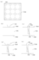
- FIG. 1 A thin plate thermistor according to a first embodiment of the present invention will be described in detail below with reference to Figures 1 to 3. Note that Figures 1 to 3 and Figures 4 to 8 used in the following description are illustrated using the same X-axis, Y-axis, and Z-axis.
- Fig. 1(a) is a perspective view of the thin plate thermistor 5
- Fig. 1(b) is a cross-sectional view taken along line B-B of the thin plate thermistor 5 shown in Fig. 1(a).
- Fig. 2(a) is a plan view showing the first main surface 51a, which is one of the main surfaces, of the thin plate thermistor 5 shown in Fig. 1
- Fig. 2(b) is a plan view showing the second main surface 51b, which is the main surface (other main surface) on the opposite side (back side) to the first main surface 51a, of the thin plate thermistor 5 shown in Fig. 1.
- the electrodes common electrode 52, split electrodes 53
- the thermistor plate 51 is not hatched.
- the thin plate thermistor 5 is a thin NTC (Negative Temperature Coefficient) thermistor.
- An NTC thermistor is a type of thermistor whose resistance value decreases as the temperature increases.
- the thin plate thermistor 5 is configured to have a thermistor plate 51 which is a single plate, a common electrode 52 which is formed on the first main surface 51a of the thermistor plate 51 and serves as a relay electrode, and a polarized electrode 53 which is formed on the second main surface 51b of the thermistor plate 51 by dividing it on the second main surface 51b and serves as an operating electrode.
- the thermistor plate 51 is thin and rectangular in plan view.
- a semiconductor ceramic plate whose main component is manganese or a semiconductor ceramic plate whose main components are manganese and nickel is used as the thermistor plate 51.
- the first main surface 51a (the center of the first main surface 51a) has a larger surface roughness than the second main surface 51b.
- the surface roughness of the center of the main surface (first main surface 51a, second main surface 51b) on which most of the electrodes (common electrode 52, split electrode 53) are formed is compared.
- the surface roughness is smaller at the ends than at the center.
- the surface roughness is greatest in the order of the center of the first main surface 51a, the second main surface 51b, and the ends of the first main surface 51a (surface roughness of the center of the first main surface 51a > surface roughness of the second main surface 51b > surface roughness of the ends of the first main surface 51a).
- the ends of the first main surface 51a, the second main surface 51b, and the center of the first main surface 51a are smooth surfaces in that order.
- the first main surface 51a of the thermistor plate 51 has a protuberance at least on a part of the edge.
- This protuberance is formed by a solidified portion 51D that solidifies after the thermistor plate 51 (the thermistor plate wafer 51A that is the basis of the thermistor plate 51) melts, and the solidified portion 51D is a laser mark (see FIG. 3).
- the common electrode 52 is formed on the entire surface (or almost the entire surface) of the first main surface 51a of the thermistor plate 51.
- the common electrode 52 is a thin metal film, and is a PVD (Physical Vapor Deposition) film formed by a PVD film formation method such as sputtering or vacuum deposition.
- PVD Physical Vapor Deposition
- the split electrodes 53 are arranged along one direction of the second main surface 51b of the thermistor plate 51, split into two at both ends with a certain distance between them.
- one of the split electrodes 53 may be referred to as the "first split electrode 53a” and the other as the “second split electrode 53b".
- the split electrodes 53 are thin metal films, and are PVD films formed by a PVD film formation method such as sputtering or vacuum deposition. By forming the common electrode 52 and split electrodes 53 (first split electrode 53a, second split electrode 53b) as PVD films, an extremely thin plate thermistor 5 can be made.
- the thin plate thermistor 5 has terminals as resistors formed by the first split electrode 53a and the second polarized electrode 53b formed on the second main surface 51b of the thermistor plate 51.
- the conductive path of the thin plate thermistor 5 is a path from one of the first split electrode 53a and the second polarized electrode 53b to the other of the first split electrode 53a and the second polarized electrode 53b via the common electrode 52. This configuration allows the cross-sectional area of the conductive path to be increased, and also allows the conductive path to be a path in which the first polarized electrode 53a and the second split electrode 53b and the common electrode 52 face each other.
- the thin plate thermistor 5 When the thin plate thermistor 5 is configured such that the distance between the first divided electrode 53a and the second divided electrode 53b is small, depending on the applied voltage, the conductive path from one of the first and second polarized electrodes 53a and 53b to the other of the first and second polarized electrodes 53a and 53b (this path does not include the common electrode 52) becomes dominant, and the desired resistance value may not be obtained. Therefore, as shown in FIG.
- the total area of the first split electrode 53a and the second split electrode 53b is within the range of 40% to 85% of the area of the second main surface 51b of the thermistor plate 51.
- the thin plate thermistor 5 can perform stable temperature detection. If the total area of the first split electrode 53a and the second split electrode 53b is less than 40% of the area of the second main surface 51b of the thermistor plate 51, the first split electrode 53a and the second split electrode 53b of the thin plate thermistor 5 will be too small, and the resistance value of the thin plate thermistor 5 will be too high, which may make it impossible to accurately detect the temperature of the device to be detected.
- the total area of the first split electrode 53a and the second split electrode 53b exceeds 85% of the area of the second main surface 51b of the thermistor plate 51, a short circuit may occur between the first split electrode 53a and the second split electrode 53b, causing the thermistor to no longer function as a thermistor.
- a material mainly composed of manganese or mainly composed of manganese and nickel (such as Mn-Fe-Ni-Ti material or Mn-Fe material) is made into a slurry with a binder or the like, and a wafer-like green sheet of the thermistor plate 51 is created using a pressure film forming technique such as screen printing or doctor blade technology, and this is then sintered and molded into the wafer 51A that will become the thermistor plate 51 using a firing technique (sintering and molding process).
- a firing technique sintered and molded into the wafer 51A that will become the thermistor plate 51 using a firing technique (sintering and molding process).
- the green sheet is placed on a firing setter made of alumina (Al 2 O 3 ) and fired, but if the firing temperature is higher than the melting point of manganese, the manganese contained in the green sheet melts into the firing setter.
- alumina Al 2 O 3
- the first surface 51aA (the surface that becomes the first main surface 51a of the thermistor flat plate 51), which is the surface of the thermistor flat plate wafer 51A that was in contact with the firing setter
- the second surface 51bA (the surface that becomes the second main surface 51b of the thermistor flat plate 51), which is the surface opposite (back side) to the surface that was in contact with the firing setter
- the first surface 51aA of the thermistor flat plate wafer 51A has a larger surface roughness than the second surface 51bA because manganese has melted out of the first surface 51aA.
- break line forming process is carried out to form break lines (small grooves) 51B in the thermistor plate wafer 51A.
- the thermistor flat plate wafer 51A is irradiated from the first surface 51aA with a laser LA1 having a small irradiation area and a large power density (W/ cm2 ) as shown in Fig. 3(b) at the portion indicated by the dotted line in Fig. 3(a), and a break line 51B shown in Fig. 3(c) that does not penetrate the thermistor flat plate wafer 51A is formed on the first surface 51aA (first stage laser irradiation).
- the break line 51B is formed by this first stage laser irradiation, as shown in Fig. 3(c)
- steep and tall burrs 51C are formed at both ends of the break line 51b of the thermistor flat plate wafer 51A, and chipping is likely to occur at the burr 51C portion.
- the thermistor flat plate wafer 51A is irradiated with a laser LA2 having a large irradiation area and a small power density (W/cm 2 ) as shown in FIG. 3(d) from the first surface 51aA side on which the break lines 51B are formed, at the portion indicated by the dotted line in FIG. 3(a) (second-stage laser irradiation).
- the irradiation area in the second-stage laser irradiation is larger than that in the first-stage laser irradiation, and the power density (W/cm 2 ) in the second-stage laser irradiation is smaller than that in the first-stage laser irradiation.
- the second-stage laser irradiation melts the burrs 51C, and the melted portion subsequently solidifies, forming a solidified portion 51D as a laser mark.
- the surface roughness is smaller at the ends than at the center, and a slight protrusion (a protrusion lower than the height of the burrs 51C) is formed in at least a portion of the ends, thereby ensuring a curved surface at the ends.
- the surface roughness of the end of the area surrounded by the break lines 51B on the first surface 51aA is the smallest
- the surface roughness of the second surface 51bA is the second smallest
- the surface roughness of the center of the area surrounded by the break lines 51B on the first surface 51aA is the largest.
- the thermistor flat plate wafer 51A may be irradiated with a laser from the first surface 51aA side on which the break line 51B is formed to the dotted line in the dashed line in FIG. 3(a) to make the depth of the break line 51B deeper or penetrate the laser irradiated portion (intermediate stage laser irradiation). In this way, when the thermistor flat plate wafer 51 is broken along the break line 51B, damage to the thin plate thermistor 5 can be suppressed.
- the irradiation area in the intermediate stage laser irradiation the irradiation area in the first stage laser irradiation ⁇ the irradiation area in the second stage laser irradiation, and the value of the light intensity per unit area in the intermediate stage laser irradiation ⁇ the power density in the first stage laser irradiation (W/cm 2 ) > the power density in the second stage laser irradiation (W/cm 2 ).
- an electrode forming process is performed in which electrodes (common electrode 52, first divided electrode 53a, second divided electrode 53b) are formed on the thermistor flat plate wafer 51A.
- an electrode film (metal film) is formed by sputtering on a predetermined area (area surrounded by break lines 51B on the first surface 51aA) of the thermistor flat plate wafer 51A after the break line forming process, and patterned using photolithography technology to form the common electrode 52
- an electrode film (metal film) is formed by sputtering on a predetermined area (area behind the area surrounded by break lines 51B on the first surface 51aA) of the thermistor flat plate wafer 51A after the break line forming process, and patterned using photolithography technology to form the first divided electrode 53a and the second divided electrode 53b.
- a laminated film structure is adopted in which a Ti film is formed as a base layer, a NiTi film made of an alloy of Ni and Ti is formed as an upper layer (middle layer), and an Au film is formed as a main layer (top layer) on the surface.
- a laminated film structure of a Ti film, a NiTi film, and a Au film is adopted, when the thin plate thermistor 5 is finally soldered to a mounting board, solder erosion is unlikely to occur and a stable conductive bond can be achieved.
- a TiO2 film may be formed between the base layer (Ti film) and the middle layer (NiTi film).
- the metal film configurations of the first polarization electrode 53 a and the second split electrode 53 b may be different from those of the common electrode 52.
- the metal film configurations of the first polarization electrode 53 a and the second split electrode 53 b may be a laminated film configuration of a Ti film, a NiTi film, and an Au film
- the film configuration of the common electrode 52 may be a laminated film configuration of a Ti film and an Au film.
- a Cr film or Ti film may be formed as an underlayer, and a laminated film configuration of an Au film, an Ag film, a Pt film, etc. may be formed on top of it, or a film configuration using only a Cu film may be formed. Note that when a laminated film configuration of an underlayer of a Cr film or Ti film and an Au film, an Ag film, a Pt film, or a single layer film configuration of a Cu film is adopted, they can be joined with a conductive resin adhesive.
- the thermistor plate wafer 51A on which the common electrode 52, the first divided electrode 53a, and the second divided electrode 53b are formed is broken along the break lines 51B (breaking process). This results in individual thin plate thermistors 5 on which the common electrode 52, the first divided electrode 53a, and the second divided electrode 53b are formed, thereby completing the thin plate thermistors 5.
- the surface roughness of the first main surface 51a of the thermistor plate 51 is smaller at the ends than at the center, so cracks and chips are less likely to occur on the first main surface 51a side of the ends of the thermistor plate 51, and as a result, the mechanical strength of the thin plate thermistor 5 can be improved.
- at least a portion of the end of the first main surface 51a of the thermistor plate 51 is raised, so cracks and chips are less likely to occur on the first main surface 51a side of the ends of the thermistor plate 51, and as a result, the mechanical strength of the thin plate thermistor 5 can be improved.
- the surface condition of the end of the first main surface 51a of the thermistor plate 51 can be smoothed to ensure a curved surface, which makes it less likely for cracks or chips to occur on the first main surface 51a side of the end of the thermistor plate 51, thereby improving the mechanical strength of the thin plate thermistor 5.
- the solidified portion 51D as a laser mark, a curved surface can be easily formed at the solidified portion 51D.
- the first and second split electrodes 53a and 53b which serve as the working electrodes, are formed on the second main surface 51b of the thermistor plate 51, which has the smaller surface roughness, the areas on which the first and second split electrodes 53a and 53b are formed are less likely to vary compared to when the first and second split electrodes 53a and 53b, which serve as the working electrodes, are formed on the first main surface 51a, which has the larger surface roughness, and this makes it possible to suppress variations in the resistance characteristics of the thin plate thermistor 5.
- the resistance characteristics of the thin plate thermistor 5 are determined by the areas of the first and second split electrodes 53a and 53b facing the thermistor plate 51, forming the first and second split electrodes 53a and 53b, which require precise areas, on the second main surface 51b, which has the smaller surface roughness, is advantageous for stabilizing the resistance characteristics of the thin plate thermistor 5.
- the adhesion of the first split electrode 53a and the second split electrode 53b to the second main surface 51b of the thermistor plate 5 is improved and the conductivity is stabilized, allowing a stable connection when a measurement probe or the like is brought into contact with the first split electrode 53a and the second split electrode 53b, making it possible to accurately measure the resistance characteristics of the thin plate thermistor 5.
- the common electrode 52 which serves as a relay electrode
- the surface area of the portion where the common electrode 52 is formed increases relative to the apparent area, and the total amount of conductors related to the common electrode 52 increases accordingly, improving the electrical conductivity.
- the common electrode 52 plays a role in preventing unnecessary resistance values from occurring in the thin plate thermistor 5, and the electrical conductivity does not decrease as the surface area of the common electrode 52 increases, so the resistance value of the thin plate thermistor 5 is not deteriorated.
- the first split electrode 53a, the second split electrode 53b, and the common electrode 52 are PVD films formed by a PVD film formation method such as sputtering or vacuum deposition, the first split electrode 53a, the second split electrode 53b, and the common electrode 52 have a dense film configuration, making them electrodes with excellent conductivity and adhesion to the thermistor plate 5.
- the electrodes can be formed so that they have a desired area, and as a result, the resistance characteristics of the thin plate thermistor 5 can be stabilized.This is particularly effective in stabilizing the resistance characteristics of a miniaturized thin plate thermistor 5.
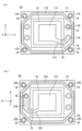
- FIG. 4 is a plan view of a piezoelectric vibration device 1 equipped with a thin plate thermistor.
- FIG. 5 is a cross-sectional view of the device 1 shown in the plan view in FIG. 4, taken along the line A-A.
- the piezoelectric vibration device 1 equipped with a thin plate thermistor is a device having a sandwich-structured piezoelectric vibration device (hereinafter also referred to as a "sandwich-structured device") 2 and the above-mentioned thin plate thermistor 5 mounted on the sandwich-structured device 2.
- the "thin plate thermistor-equipped piezoelectric vibration device 1" may simply be referred to as “device 1.”
- the thickness of the sandwich-structured device 2 is about 120 ⁇ m, while the thin plate thermistor 5 can be less than half the thickness of the sandwich-structured device 2 (about 50 ⁇ m).
- the sandwich structure device 2 is configured with a piezoelectric diaphragm 10, a first sealing member 20, and a second sealing member 30.
- the piezoelectric diaphragm 10 and the first sealing member 20 are bonded together, and the piezoelectric diaphragm 10 and the second sealing member 30 are bonded together, thereby forming a substantially rectangular sandwich structure package.
- FIG. 6(a) is a plan view showing the first main surface 11, which is one of the main surfaces (the surface to be bonded to the first sealing member 20) of the single piezoelectric diaphragm 10 before bonding.
- FIG. 6(b) is a plan view showing the second main surface 12, which is the other main surface (the surface to be bonded to the second sealing member 30) of the single piezoelectric diaphragm 10 before bonding.
- the piezoelectric diaphragm 10 is a piezoelectric substrate made of a piezoelectric material such as quartz, and both main surfaces (first main surface 11, second main surface 12) are formed as flat, smooth surfaces (mirror-finished). In this embodiment, an AT-cut quartz plate that performs thickness-shear vibration is used as the piezoelectric diaphragm 10.
- both main surfaces of the piezoelectric diaphragm 10 are in the XZ plane, the direction parallel to the short side direction is the X-axis direction, the direction parallel to the long side direction is the Z-axis direction, and the direction perpendicular to the XZ plane is the Y-axis direction.
- the piezoelectric diaphragm 10 has a vibration part 13 formed in a substantially rectangular shape, an outer frame part 14 that surrounds the outer periphery of the vibration part 13, and a holding part 15 that holds the vibration part 13 by connecting the vibration part 13 and the outer frame part 14.
- the area between the vibration part 13 and the outer frame part 14 is a cutout part (an opening that penetrates the piezoelectric diaphragm 10 in the thickness direction) except for the part where the holding part 15 is formed.
- the piezoelectric diaphragm 10 is configured such that the vibration part 13, the outer frame part 14, and the holding part 15 are integrally provided.
- a pair of excitation electrodes (a first excitation electrode 111 on the first main surface 11 side and a second excitation electrode 121 on the second main surface 12 side) are formed on the first main surface 11 and the second main surface 12 of the piezoelectric diaphragm 10.
- the holding portion 15 is provided at only one location between the vibration portion 13 and the outer frame portion 14. Furthermore, the vibration portion 13 and the holding portion 15 are formed thinner than the outer frame portion 14. Due to this difference in thickness between the outer frame portion 14 and the holding portion 15, the natural frequencies of the piezoelectric vibrations of the outer frame portion 14 and the holding portion 15 are different, and the piezoelectric vibrations are not propagated to the outer frame portion 14. Note that the location where the holding portion 15 is formed is not limited to one location, and the holding portion 15 may be provided at two locations between the vibration portion 13 and the outer frame portion 14.
- the first excitation electrode 111 is provided on the first main surface 11 side of the vibration part 13, and the second excitation electrode 121 is provided on the second main surface 12 side of the vibration part 13.
- the first excitation electrode 111 and the second excitation electrode 121 are each connected to an extraction electrode (extraction wiring electrode film) (the first extraction electrode 112 on the first main surface 11 side, and the second extraction electrode 122 on the second main surface 12 side) for connecting these excitation electrodes to external electrode terminals.
- the first extraction electrode 112 is extracted from the first excitation electrode 111 and connected to the connection bonding pattern 114 formed on the outer frame part 14 via the holding part 15.
- the second extraction electrode 122 is extracted from the second excitation electrode 121 and connected to the connection bonding pattern 124 formed on the outer frame part 14 via the holding part 15.
- the first main surface 11 and the second main surface 12 of the piezoelectric diaphragm 10 are each formed with a bonding pattern for bonding the piezoelectric diaphragm 10 to the first sealing member 20 and the second sealing member 30.
- the bonding pattern includes a sealing pattern for hermetically sealing the internal space of the package, and a conductive pattern for conducting wiring and electrodes. Note that in Figures 6(a), (b), 7(b), and 8(a), the bonding regions where the bonding patterns are formed are indicated by diagonal hatching.
- a vibration-side first bonding pattern 113 is formed on the first main surface 11, and a vibration-side second bonding pattern 123 is formed on the second main surface 12.
- the vibration-side first bonding pattern 113 and the vibration-side second bonding pattern 123 are provided on the outer frame portion 14 and are formed in a ring shape in a planar view.
- the area inside the vibration-side first bonding pattern 113 and the vibration-side second bonding pattern 123 becomes the sealing area of the vibration portion 13 (the area that becomes the internal space of the package after bonding).
- the first excitation electrode 111 and the second excitation electrode 121 are not electrically connected to the vibration-side first bonding pattern 113 and the vibration-side second bonding pattern 123.
- connection bonding patterns 115 are formed outside the sealing area (outside the vibration side first bonding pattern 113), and connection bonding patterns 114 and 116 are formed within the sealing area (inside the vibration side first bonding pattern 113).
- connection bonding patterns 125 are formed outside the sealing area (outside the vibration side second bonding pattern 123), and connection bonding pattern 124 is formed within the sealing area (inside the vibration side second bonding pattern 123).
- the connection bonding patterns 115 on the first main surface 11 side and the connection bonding patterns 125 on the second main surface 12 side are provided in areas near the four corners (corners) of the outer frame portion 14, respectively.
- the piezoelectric diaphragm 10 has a plurality of through holes 16 formed between the first main surface 11 and the second main surface 12, and a through electrode is formed on the inner wall surface of each through hole 16 to provide electrical continuity between the first main surface 11 and the second main surface 12.
- a through electrode is formed on the inner wall surface of each through hole 16 to provide electrical continuity between the first main surface 11 and the second main surface 12.
- four through holes 16 and through electrodes are formed to provide electrical continuity between the connection bonding pattern 115 and the connection bonding pattern 125, and one through hole 16 and through electrode is formed to provide electrical continuity between the connection bonding pattern 116 and the connection bonding pattern 124.
- the first excitation electrode 111, the second excitation electrode 121, the first extraction electrode 112, the second extraction electrode 122, the vibration side first bonding pattern 113, the vibration side second bonding pattern 123, and the connection bonding patterns 114 to 116, 124, and 125 can be formed in the same process. Specifically, they can be formed from an underlayer (Ti film) formed by physical vapor deposition on both main surfaces (first main surface 11, second main surface 12) of the piezoelectric diaphragm 10, and a bonding film (Au film) formed by physical vapor deposition on the underlayer.
- the configuration of the laminated film forming the bonding pattern is not limited to a two-layer structure of a Ti film and an Au film, but may be a three-layer or more structure including other films (for example, a barrier film formed between the Ti film and the Au film).
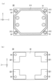
- Figure 7(a) is a plan view showing the first main surface 21, which is one of the main surfaces (outer surface) of the single first sealing member 20 before bonding.
- Figure 7(b) is a plan view showing the second main surface 22, which is the other main surface (the bonding surface with the piezoelectric diaphragm 10) of the single first sealing member 20 before bonding.
- the first sealing member 20 is a rectangular substrate formed from a single glass wafer or quartz wafer, and the second main surface 22 of this first sealing member 20 is formed as a flat and smooth surface (mirror finish).
- the electrode pattern 211 is a mounting pad for mounting the thin plate thermistor 5 (see FIG. 4).
- the wiring pattern 212 is a wiring pattern that is part of the wiring path that connects the second excitation electrode 121 to the external electrode terminal 321 (see FIG. 8(b)).
- the wiring pattern 213 is a wiring pattern that is part of the wiring path that connects the first excitation electrode 111 to the external electrode terminal 321.
- a bonding pattern is formed on the second main surface 22 of the first sealing member 20 for bonding the first sealing member 20 to the piezoelectric diaphragm 10.
- This bonding pattern includes a sealing pattern for hermetically sealing the internal space of the package, and a conductive pattern for conducting wiring and electrodes.
- the sealing pattern in the first sealing member 20 is a sealing-side first bonding pattern 221.
- the sealing-side first bonding pattern 221 is formed in a ring shape in a plan view, and its inner region becomes the sealing region.
- four connection bonding patterns 222 are formed near the four corners (corners) outside the sealing region (outside the sealing-side first bonding pattern 221), and connection bonding patterns 223 to 225 are formed within the sealing region (inside the sealing-side first bonding pattern 221).
- the connection bonding pattern 224 and the connection bonding pattern 225 are connected by a wiring pattern 226.
- the first sealing member 20 has a plurality of through holes 23 formed between the first main surface 21 and the second main surface 22, and a through electrode is formed on the inner wall surface of each through hole 23 to provide electrical continuity between the first main surface 21 and the second main surface 22.
- four through holes 23 and through electrodes are formed to provide electrical continuity between the electrode pattern 211 or the wiring patterns 212, 213 and the connection bonding pattern 222, one through hole 23 and through electrode are formed to provide electrical continuity between the wiring pattern 212 and the connection bonding pattern 223, and one through hole 23 and through electrode are formed to provide electrical continuity between the wiring pattern 213 and the connection bonding pattern 225.
- the sealing-side first bonding pattern 221, the connection bonding patterns 222 to 225, and the wiring pattern 226 can be formed in the same process. Specifically, they can be formed from an underlayer (Ti film) formed by physical vapor deposition on the second main surface 22 of the first sealing member 20, and a bonding film (Au film) formed by physical vapor deposition on the underlayer.
- underlayer Ti film
- Au film bonding film
- Figure 8(a) is a plan view showing the first main surface 31, which is one of the main surfaces (the surface to be bonded to the piezoelectric diaphragm 10), of the second sealing member 30 alone before bonding.
- Figure 8(b) is a plan view showing the second main surface 32, which is the other main surface (outer surface) of the second sealing member 30 alone before bonding.
- the second sealing member 30 is a rectangular substrate formed from a single glass wafer or quartz wafer, and the first main surface 31 of this second sealing member 30 is formed as a flat and smooth surface (mirror-finished).
- a bonding pattern is formed on the first main surface 31 of the second sealing member 30 for bonding the second sealing member 30 to the piezoelectric diaphragm 10.
- This bonding pattern includes a sealing pattern for hermetically sealing the internal space of the package, and a conductive pattern for conducting wiring and electrodes.
- the sealing pattern in the second sealing member 30 is a sealing-side second bonding pattern 311.
- the sealing-side second bonding pattern 311 is formed in a ring shape in a plan view, and its inner region becomes the sealing region.
- four connection bonding patterns 312 are formed near the four corners (corners) outside the sealing region (outside the sealing-side second bonding pattern 311).
- the second main surface 32 of the second sealing member 30 is provided with four external electrode terminals 321 that electrically connect the device 1 to the outside.
- the external electrode terminals 321 are located at the four corners (corner portions) of the second sealing member 30.
- the second sealing member 30 has a plurality of through holes 33 formed between the first main surface 31 and the second main surface 32, and a through electrode is formed on the inner wall surface of each through hole 33 to provide electrical continuity between the first main surface 31 and the second main surface 32. Specifically, four through holes 33 and through electrodes are formed to provide electrical continuity between the connection bonding pattern 312 and the external electrode terminal 321.
- the sealing-side second bonding pattern 311 and the bonding bonding pattern 312 can be formed by the same process. Specifically, they can be formed from a base layer (Ti film) formed by physical vapor deposition on the first main surface 31 of the second sealing member 30, and a bonding film (Au film) formed by physical vapor deposition on the base layer.
- a base layer Ti film
- Au film bonding film
- the piezoelectric diaphragm 10 and the first sealing member 20 are diffusion bonded with the vibration side first bonding pattern 113 and the sealing side first bonding pattern 221 overlapping each other, and the piezoelectric diaphragm 10 and the second sealing member 30 are diffusion bonded with the vibration side second bonding pattern 123 and the sealing side second bonding pattern 311 overlapping each other, to manufacture a sandwich structure package.
- the vibration side first bonding pattern 113 and the sealing side first bonding pattern 221 are bonded to form a sealing pattern layer between the piezoelectric diaphragm 10 and the first sealing member 20, and the vibration side second bonding pattern 123 and the sealing side second bonding pattern 311 are bonded to form a sealing pattern layer between the piezoelectric diaphragm 10 and the second sealing member 30.
- connection bonding patterns which are conductive patterns
- the connection bonding patterns are also bonded together, and the bonded conductive patterns form a conductive pattern layer between the piezoelectric diaphragm 10 and the first sealing member 20 or between the piezoelectric diaphragm 10 and the second sealing member 30.
- electrical conduction is achieved between the first excitation electrode 111 and the second excitation electrode 121 and the external electrode terminals 321 at the lower right and upper left of Figure 8 (b).
- the thin plate thermistor 5 is mounted on the sandwich structure device 2 with the second main surface 51b, on which the split electrode 53 is formed, as the underside (the joining surface with the sandwich structure device 2), and the split electrode 53 is electrically joined to the electrode pattern 211 of the first sealing member 20.
- the thin plate thermistor 5 mounted on the sandwich structure device 2 is also arranged to be electrically conductive with the external electrode terminals 321 at the upper right and lower left of Figure 8 (b).
- the thin plate thermistor 5 has wide-area metal electrodes (common electrode 52, split electrodes 53), and thus can act advantageously as a shielding member for the sandwich structure device 2.
- the thin plate thermistor 5 is arranged in the sandwich structure device 2 so that, in a plan view of the device 1, at least a portion of the thin plate thermistor 5 overlaps with the vibrating portion 13 of the sandwich structure device 2 (see FIG. 4).
- the thin plate thermistor 5 is arranged so that it overlaps with the entire first excitation electrode 111 and the second excitation electrode 121 in a plan view, the shielding effect of the thin plate thermistor 5 can be maximized, which is more preferable.
- the thin plate thermistor 5 is arranged in the sandwich structure device 2 so that both ends overlap the outer frame portion 14 at least on two opposing sides of the sandwich structure device 2.
- the first sealing member 20 and the second sealing member 30 in the sandwich structure device 2 are extremely thin substrates, and brittle materials such as glass and quartz are used. For this reason, the strength of the sandwich structure device 2 is particularly low in the center (the area where the outer frame portion 14 of the piezoelectric diaphragm 10 does not exist). In such a sandwich structure device 2, if the thin plate thermistor 5 is arranged in the center area of the sandwich structure device 2, there is a risk that the first sealing member 20 will crack due to the pressing force when mounting the thin plate thermistor 5.
- the thin plate thermistor 5 may also overlap the outer frame portion 14 on two sides facing in the long direction of the sandwich structure device 2. Furthermore, the thin plate thermistor 5 may be arranged so as to overlap not only two opposing sides of the sandwich structure device 2, but also three or four sides.
- the split electrodes 53 and the electrode patterns 211 are electrically connected by a conductive resin adhesive 61 (see FIG. 5). However, this is not limited to this, and the split electrodes 53 and the electrode patterns 211 may be connected by Au (gold) bumps. Furthermore, the gap between the thin plate thermistor 5 and the sandwich structure device 2 (the gap where the conductive resin adhesive 61 is not present) is filled with a non-conductive resin adhesive 62 (see FIG. 5).
- the non-conductive resin adhesive 62 may not only be filled on the underside of the thin plate thermistor 5, but may also be used as a sealing resin that seals the entire thin plate thermistor 5. Note that a silicone-based resin can be used as the conductive resin adhesive 61, and an epoxy-based resin can be used as the non-conductive resin adhesive 62.
- the thermal conductivity between the thin plate thermistor 5 and the sandwich structure device 2 can be improved. This allows the thin plate thermistor 5 to be maintained at a temperature close to that of the vibrating part 13 of the sandwich structure device 2.
- Surface bonding between the sandwich structure device 2 and the thin plate thermistor 5 also has the advantage of improving the strength of the device 1.
- the conductive resin adhesive 61 and the non-conductive resin adhesive 62 are used to bond the thin plate thermistor 5, it is preferable that the conductive resin adhesive 61 has a higher thermal conductivity than the non-conductive resin adhesive 62. This can further improve the thermal conductivity between the thin plate thermistor 5 and the sandwich structure device 2.
- the thin plate thermistor 5 is surface-bonded to the first main surface 21 of the first sealing member 20 by the conductive resin adhesive 61 and the non-conductive resin adhesive 62 over more than half (50% to 100%) of the area of the thin plate thermistor 5 in a plan view.
- the non-conductive resin adhesive 62 has a higher hardness than the conductive resin adhesive 61. This can relieve stress between the thin plate thermistor 5 and the sandwich structure device 2 and improve the package strength of the device 1.
- the above-mentioned piezoelectric vibration device 1 equipped with a thin plate thermistor is less likely to crack or chip at the end of the thermistor plate 51, and by providing the thin plate thermistor 5 of the first embodiment, which has excellent resistance characteristics, it is possible to improve the temperature detection accuracy.
- the first main surface 51a of the thin plate thermistor 5 is disposed so as to be the surface opposite to the surface facing the sandwich structure device 2 (piezoelectric vibration plate 10), and by disposing at least a solidified portion 51D (curved surface) on the outer surface of the thin plate thermistor 5, the end of the thin plate thermistor 5 is less likely to crack or chip, which is desirable in terms of increasing mechanical strength.
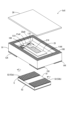
- FIG. 9 is an exploded perspective view of a thin plate thermistor-mounted piezoelectric vibration device XcX.
- Fig. 10 is a bottom view of the thin plate thermistor-mounted piezoelectric vibration device XcX shown in the exploded perspective view of Fig. 9.
- Fig. 11 is a CC cross-sectional view of the thin plate thermistor-mounted piezoelectric vibration device XcX of Fig. 10.
- the thin plate thermistor-mounted piezoelectric vibration device XcX is a device having a package 1X with an upper storage section 11AX and a lower storage section 11BX, a piezoelectric vibration plate 2X stored in the upper storage section 11AX, the above-mentioned thin plate thermistor 5 stored in the lower storage section 11BX, and a lid 3X that hermetically seals the upper storage section 11A.
- the package 1X is made of ceramic and has a rectangular parallelepiped shape overall, with an upper storage section 11AX that opens upward and a lower storage section 11BX that opens downward.
- the upper storage section 11AX and the lower storage section 11BX are configured so that their closed portions (bottoms) are back-to-back with respect to the substrate 11CX.
- the upper storage section 11AX has a concave rectangular storage configuration that opens upward, and mounting electrodes 16X, 17X made of a metal film are formed on the bottom of the upper storage section 11AX.
- the mounting electrodes 16X, 17X are formed side by side in a direction that follows the short side of the package 1X.
- a rectangular sealing section 10X is provided on the outer periphery of the upper storage section 11AX, and is located higher than the bottom, and a metal film layer is formed on the sealing section 10X.
- Mount electrodes 16X, 17X are made of multiple metal films, and are laminated in the order of a W (tungsten) layer, a Ni (nickel) layer, and a Au (gold) layer.
- the W layer is integrally formed by firing with the ceramic material that constitutes the package, and the Ni layer and Au layer are formed on the W layer by plating.
- Sealing section 10X also has a metal layer configuration similar to that of mounting electrodes 16X, 17X, with a laminated configuration of a W layer, a Ni layer, and a Au layer laminated in that order.
- mounting electrodes 18X, 19X and mounting electrodes 12X, 13X, 14X, and 15X are also manufactured using the same manufacturing method, and each has a laminated configuration of a W layer, a Ni layer, and a Au layer laminated in that order.
- Lower storage section 11BX has a concave rectangular storage configuration that opens downward, and mounting electrodes 18X, 19X made of metal film are formed on the bottom of lower storage section 11BX.
- Mounting electrodes 18X, 19X are rectangular with long and short sides, and are formed so that the long side of mounting electrode 18X faces the long side of mounting electrode 19X in the direction along the long side of package 1X.
- Mounting electrodes 18X, 19X may also be formed so that they are aligned in the direction along the short side of package 1X.
- the four corners of the lower storage section 11BX are provided with mounting electrodes 12X, 13X, 14X, and 15X that are located higher than the bottom.
- Each of the mounting electrodes 12X, 13X, 14X, and 15X has a rectangular shape, and the mounting electrodes 12X and 14X are electrically connected to the mounting electrodes 16X and 17X, and the mounting electrodes 13X and 15X are electrically connected to the mounting electrodes 18X and 19X by internal wiring within the package 1X.
- Excitation electrodes 21X and 22X are formed in the center of the front and back of the piezoelectric diaphragm 2X, and the excitation electrodes 21X and 22X are drawn to the outer periphery of the piezoelectric diaphragm 2X by strip-shaped lead electrodes 21aX and 22aX having a width.
- the excitation electrodes 21X and 22X are rectangular, and on one main surface of the piezoelectric diaphragm 2X, the excitation electrode 21X is drawn from one short corner to an end of one main surface of the piezoelectric diaphragm 2X by the lead electrode 21aX, and on the other main surface of the piezoelectric diaphragm 2X, the excitation electrode 22X is drawn from one short corner to an end of the other main surface of the piezoelectric diaphragm 2X by the lead electrode 22aX. As a result, the excitation electrodes 21X and 22X are drawn to one short side of the piezoelectric diaphragm 2X.
- the excitation electrodes 21X, 22X and the extraction electrodes 21aX, 22aX are configured by laminating thin metal films, with a Ti (titanium) layer formed in contact with the piezoelectric diaphragm 2X and an Au (gold) layer formed on top of that.
- the metal film configuration may be other than that described above, and well-known metal film configurations may be used, such as a Cr (chromium) layer as the base metal and an Ag (silver) layer as the upper layer.
- the excitation electrodes 21X, 22X and the extraction electrodes 21aX, 22aX may be PVD films formed by a PVD film formation method such as sputtering or vacuum deposition.
- the thin plate thermistor 5 has the second main surface 51b on which the split electrodes 53 are formed as the upper surface (the surface to be joined to the package 1X), and the split electrodes 53 (the first and second split electrodes 53
- the semiconductor device is mounted on the package 1X by electrically connecting the mounting electrodes 18X and 19X at the bottom of the lower storage portion 11BX to the mounting electrodes 18X and 19X at the bottom of the lower storage portion 11BX.
- the lid 3X is made of a thin metal or ceramic plate and has a rectangular shape corresponding to the outer size of the sealing part 10X of the package 1X.
- the configurations of the lid 3X and the sealing part 10X differ depending on the airtight sealing method of the package 1X.
- the lid 3X uses Kovar as the core material and has a Ni plating film formed on its surface.
- the sealing part 10X is configured by soldering a ring-shaped metal frame, and the lid 3X and the metal frame (sealing part 10X) are joined by seam welding in a vacuum atmosphere or an inert gas atmosphere, for example. This allows the inside of the package 1X (inside the upper storage part 11AX) to be in a steady state of a vacuum atmosphere or an inert gas atmosphere.
- the AuSu brazing material When hermetically sealing by soldering with a metal brazing material, for example an AuSu brazing material, the AuSu brazing material is preformed around the lid 3X, and the upper layer of the sealing portion 10X is plated with Au. By heating both of them in a specified atmosphere and temperature environment, a hermetic seal can be achieved by metal brazing.
- a metal brazing material for example an AuSu brazing material
- a paste-like conductive resin adhesive S1 is applied to the mounting electrodes 16X and 17X of the upper storage section 11AX of the package 1X using a dispenser or the like.
- the conductive resin adhesive S1 is made of, for example, a silicone resin adhesive containing metal filler, but other resin materials such as polyimide-based resin materials may also be used.
- the piezoelectric diaphragm 2X with electrodes formed thereon is mounted on the applied conductive resin adhesive S1. Specifically, the piezoelectric diaphragm 2X is mounted on the upper storage section 11AX so that the extraction electrodes 21aX and 22aX are bonded to the conductive resin adhesive S1.
- the conductive resin adhesive S1 is then hardened by heating to conductively bond (electrically and mechanically bond) the piezoelectric diaphragm 2X and the mounting electrodes 16X and 17X. Note that the conductive resin adhesive S1 may be applied again from above the piezoelectric diaphragm 2X as necessary. In this embodiment, a configuration in which the adhesive is applied again is illustrated.
- the upper storage section 11AX is hermetically sealed by the lid 3X, which is achieved by joining the lid 3X to the sealing section 10X.
- the metal brazing material sealing is achieved by using the metal brazing material S2, which is, for example, an AuSu brazing material.
- the thin plate thermistor 5 is conductively joined to the lower storage section 11BX of the package 1X.
- a conductive resin adhesive S1 is applied to the mounting electrodes 18X and 19X using a dispenser or the like.
- the thin plate thermistor 5 is stored in the lower storage section 11BX so that the split electrodes 53 (first split electrode 53a, second split electrode 53b) correspond to the applied conductive resin adhesive S1.
- the conductive resin adhesive S1 is then hardened by heating to conductively join (electrically and mechanically join) the first split electrode 53a and second split electrode 53b of the thin plate thermistor 5 to the mounting electrodes 18X and 19X.
- the conductive joining of the thin plate thermistor 5 may be performed by soldering.
- Resin material M is injected into the lower storage section 11BX containing the thin plate thermistor 5 using a dispenser or the like to cover the thin plate thermistor 5 with the resin material M, and then the resin material M is hardened by heating.
- a polyimide resin is used as the resin material M, but other resin materials may also be used. This protects the thin plate thermistor 5 from the outside air, allowing for stable temperature detection.
- the above-mentioned piezoelectric vibration device XcX equipped with a thin plate thermistor is less likely to crack or chip at the end of the thermistor plate 51, and by being equipped with the thin plate thermistor 5 of the first embodiment, which has excellent resistance characteristics, it is possible to improve the accuracy of temperature detection.
- Fig. 12 is a cross-sectional view of a thin plate thermistor mounted piezoelectric vibrating device XcY.
- a piezoelectric vibration plate 2X and a thin plate thermistor 5 are stored inside a storage section 51Y of a package 1Y of the thin plate thermistor mounted piezoelectric vibration device XcY.
- the package 1Y is made of ceramic with internal wiring formed therein, and has a storage section 51Y with an opening at the top.
- Mounting electrodes 54Y, 55Y (mounting electrode 55Y not shown) for the piezoelectric vibration plate 2X and mounting electrodes 56Y, 57Y for the thin plate thermistor 5 are formed on the bottom of the storage section 51Y.
- Mounting electrodes 52Y, 53Y are also formed on the bottom surface.
- the extraction electrodes 21aX, 22aX (see FIG. 9) formed on both main surfaces of the piezoelectric diaphragm 2X are conductively bonded (electrically and mechanically bonded) to the mounting electrodes 54Y, 55Y by the conductive resin adhesive S1, and the piezoelectric diaphragm 2X is stored inside the storage section 51Y of the package 1Y.
- the first and second split electrodes 53a, 53b formed on the second main surface 51b of the thin plate thermistor 5 are conductively bonded (electrically and mechanically bonded) to the mounting electrodes 56Y, 57Y by the conductive resin adhesive S1, and the thin plate thermistor 5 is stored inside the storage section 51Y of the package 1Y.
- the piezoelectric diaphragm 2X and thin plate thermistor 5 are stored in parallel inside the storage section 51Y of the package 1Y and are hermetically sealed by the lid 3X.
- the above-mentioned piezoelectric vibration device XcY equipped with a thin plate thermistor is less likely to crack or chip at the end of the thermistor plate 51, and by being equipped with the thin plate thermistor 5 of the first embodiment, which has excellent resistance characteristics, it is possible to improve the temperature detection accuracy.
- the thin plate thermistor is not limited to the thin plate thermistor 5 of the above embodiment, but can be modified in various ways.
- the first stage laser irradiation and the second stage laser irradiation on the thermistor flat plate wafer 51 can be performed from the second surface 51bA side having the lesser surface roughness, so that the end portion of the second main surface 51b of the thermistor flat plate 51 has a smaller surface roughness than the central portion, at least a part of the end portion is raised, and the thermistor flat plate 51 has a solidified portion (another solidified portion) at the end portion of the second main surface 52b.
- the surface roughness is smaller at the end portion than at the center portion of the first main surface 51a and the second main surface 51b of the thermistor flat plate 51, and at least a part of the end portion is raised, and the thermistor flat plate 51 may have a solidified portion and another solidified portion at each end portion of the first main surface 51a and the second main surface 51b.
- the thermistor flat plate 51 is less likely to crack or chip on both the first main surface 51a side and the second main surface 51b side of the end portion of the thermistor flat plate 51, and as a result, the mechanical strength of the thin plate thermistor 5 can be further improved.
- the thin plate thermistor 5 may not include the common electrode 52.
- the thin plate thermistor 5 may not include the common electrode 52, and the first split electrode 53a and the second split electrode 53b may be replaced with a first split electrode and a second split electrode including a second main surface portion disposed on a part of the second main surface 51b of the thermistor plate 51, a side surface portion connected to the second main surface portion and disposed on a side surface of the thermistor plate 51, and a first main surface portion connected to the side surface portion and disposed on the first main surface 51a of the thermistor plate 51.
- the advantage of using the thin plate thermistor 5 is that it can be made smaller and thinner, and by combining it with the sandwich structure device 2, it is advantageous to make the device smaller and thinner, and from this perspective, it is preferable to combine the thin plate thermistor 5 with the sandwich structure device 2.
- the thin plate thermistor 5 of the above embodiment can be applied to existing packages other than the above-mentioned packages, such as sandwich structure devices. For example, it can also be applied to a molded resin sealed package.
- a piezoelectric vibration device and a thin plate thermistor are mounted flat on top of a glass epoxy substrate that serves as a base substrate, in a state where they are arranged in parallel with a bonding material, and are electrically connected to the terminal portion of the base substrate by wire bonding or the like. Then, the top including each of these components is covered with molded resin. With such a configuration, it is possible to expect improved thermal conductivity.
- a laser is used to form the solidified portion 51D at the end of the thermistor plate 51, but this is not limited to the above, and for example, a means other than a laser, such as an electron beam, may be used to form the solidified portion 51D at the end of the thermistor plate 51.
- a means other than a laser such as an electron beam
- the surface roughness of one side and the other side of the thermistor plate can be made different by flat surface polishing with different surface roughness.
- a reinforcing member that is thin and has a certain degree of structural strength such as a quartz wafer or aluminum foil, may be attached to the common electrode 52 of the thin plate thermistor 5 of the above embodiment. If a hard material, such as a quartz wafer, is used as the reinforcing member, the strength of the thin plate thermistor 5 is greatly increased, making it easier to attach the thin plate thermistor 5 to the sandwich structure device 2. When a quartz wafer is used as the reinforcing member, it is desirable to form a film on the common electrode 52 to improve adhesion.
- the reinforcing member if an insulating material is used as the reinforcing member, it is not necessary to perform an insulating process on the top surface of the device 1 (the surface opposite (back side) of the reinforcing member to the surface facing the common electrode 52) after mounting the thin plate thermistor 5 on the sandwich structure device 2.
- a sintered product obtained by sintering a pure metal such as molybdenum or tungsten as a sintering material may be disposed on the first main surface 51a of the thermistor plate 51 to serve as a common electrode.
- This improves the strength of the thin plate thermistor 5 and allows the thickness of the thermistor plate 51 to be reduced by the thickness of the sintered product used as the common electrode 52.
- Tungsten has thermal conductivity comparable to that of aluminum, which speeds up heat transfer throughout the thin plate thermistor 5 and improves the thermal response of the thin plate thermistor 5.
- Ag paste may be applied to the entire or almost entire first main surface 51a of the thermistor plate 51 and baked to form a common electrode 52 on the first main surface 51a of the thermistor plate 51.
- the common electrode 52 functions as an original relay electrode and also functions as a reinforcing member that improves the strength of the thin plate thermistor 5.
- the common electrode 52 may be formed of Cr-Au on the first main surface 51a of the thermistor plate 51, and then an epoxy resin may be provided as a reinforcing member on the surface of the common electrode 52 opposite to the surface facing the thermistor plate 51 (back side). In these cases, the strength of the thin plate thermistor 5 can be improved while preventing deterioration of the resistance characteristics of the thin plate thermistor 5.
- the present invention can be widely applied to thin plate thermistors used as temperature sensors and piezoelectric vibration devices equipped with thin plate thermistors.
- Piezoelectric vibration device with thin plate thermistor 2 Sandwich structure device 5: Thin plate thermistor 51: Thermistor plate 51a: First main surface 51b: Second main surface 51D: Solidified portion 52: Common electrode 53, 53a, 53b: Split electrodes
Landscapes
- Engineering & Computer Science (AREA)
- Microelectronics & Electronic Packaging (AREA)
- Physics & Mathematics (AREA)
- Electromagnetism (AREA)
- Manufacturing & Machinery (AREA)
- Acoustics & Sound (AREA)
- Piezo-Electric Or Mechanical Vibrators, Or Delay Or Filter Circuits (AREA)
Priority Applications (2)
| Application Number | Priority Date | Filing Date | Title |
|---|---|---|---|
| CN202380068062.3A CN119895509A (zh) | 2022-11-22 | 2023-11-16 | 薄板热敏电阻及薄板热敏电阻搭载型压电振动器件 |
| JP2024560104A JPWO2024111494A1 (https=) | 2022-11-22 | 2023-11-16 |
Applications Claiming Priority (2)
| Application Number | Priority Date | Filing Date | Title |
|---|---|---|---|
| JP2022-186193 | 2022-11-22 | ||
| JP2022186193 | 2022-11-22 |
Publications (1)
| Publication Number | Publication Date |
|---|---|
| WO2024111494A1 true WO2024111494A1 (ja) | 2024-05-30 |
Family
ID=91195647
Family Applications (1)
| Application Number | Title | Priority Date | Filing Date |
|---|---|---|---|
| PCT/JP2023/041211 Ceased WO2024111494A1 (ja) | 2022-11-22 | 2023-11-16 | 薄板サーミスタおよび薄板サーミスタ搭載型圧電振動デバイス |
Country Status (3)
| Country | Link |
|---|---|
| JP (1) | JPWO2024111494A1 (https=) |
| CN (1) | CN119895509A (https=) |
| WO (1) | WO2024111494A1 (https=) |
Citations (5)
| Publication number | Priority date | Publication date | Assignee | Title |
|---|---|---|---|---|
| JPS546768A (en) * | 1977-06-17 | 1979-01-19 | Nec Corp | Manufacture of semiconductor device |
| JP2002057009A (ja) * | 2000-08-07 | 2002-02-22 | Koa Corp | 抵抗器の製造方法および抵抗器 |
| JP2004276386A (ja) * | 2003-03-14 | 2004-10-07 | Koa Corp | 分割用セラミック基板およびその製造方法 |
| JP2006128480A (ja) * | 2004-10-29 | 2006-05-18 | Taiyosha Electric Co Ltd | チップ抵抗器の製造方法 |
| JP2013106054A (ja) * | 2011-11-10 | 2013-05-30 | Daishinku Corp | 圧電デバイス |
Family Cites Families (2)
| Publication number | Priority date | Publication date | Assignee | Title |
|---|---|---|---|---|
| JPH05335004A (ja) * | 1992-06-02 | 1993-12-17 | Matsushita Electric Ind Co Ltd | Ptc装置の製造法ならびにptc装置を備えた電池 |
| JP2011187985A (ja) * | 2004-03-31 | 2011-09-22 | Mitsubishi Materials Corp | チップ抵抗器の製造方法 |
-
2023
- 2023-11-16 JP JP2024560104A patent/JPWO2024111494A1/ja active Pending
- 2023-11-16 CN CN202380068062.3A patent/CN119895509A/zh active Pending
- 2023-11-16 WO PCT/JP2023/041211 patent/WO2024111494A1/ja not_active Ceased
Patent Citations (5)
| Publication number | Priority date | Publication date | Assignee | Title |
|---|---|---|---|---|
| JPS546768A (en) * | 1977-06-17 | 1979-01-19 | Nec Corp | Manufacture of semiconductor device |
| JP2002057009A (ja) * | 2000-08-07 | 2002-02-22 | Koa Corp | 抵抗器の製造方法および抵抗器 |
| JP2004276386A (ja) * | 2003-03-14 | 2004-10-07 | Koa Corp | 分割用セラミック基板およびその製造方法 |
| JP2006128480A (ja) * | 2004-10-29 | 2006-05-18 | Taiyosha Electric Co Ltd | チップ抵抗器の製造方法 |
| JP2013106054A (ja) * | 2011-11-10 | 2013-05-30 | Daishinku Corp | 圧電デバイス |
Also Published As
| Publication number | Publication date |
|---|---|
| JPWO2024111494A1 (https=) | 2024-05-30 |
| CN119895509A (zh) | 2025-04-25 |
Similar Documents
| Publication | Publication Date | Title |
|---|---|---|
| US11342899B2 (en) | Crystal resonator device | |
| JP2006191517A (ja) | 温度補償型圧電発振器 | |
| JP5853702B2 (ja) | 圧電振動デバイス | |
| JP2019068304A (ja) | 圧電振動デバイス | |
| JP7683725B2 (ja) | サーミスタ搭載型圧電振動デバイス | |
| JP5152012B2 (ja) | 圧電振動デバイスおよび圧電振動デバイスの製造方法 | |
| JP5101201B2 (ja) | 圧電発振器 | |
| JP7679757B2 (ja) | サーミスタ付き水晶振動デバイス | |
| JP5171148B2 (ja) | 圧電発振器 | |
| JP2000077943A (ja) | 温度補償型水晶発振器 | |
| JP7838678B2 (ja) | 薄板サーミスタおよび薄板サーミスタ搭載型圧電振動デバイス | |
| JP7703972B2 (ja) | 温度センサ付き水晶振動デバイス | |
| WO2024111494A1 (ja) | 薄板サーミスタおよび薄板サーミスタ搭載型圧電振動デバイス | |
| JP5188932B2 (ja) | 圧電発振器 | |
| JP2008289055A (ja) | シート基板とシート基板を用いた圧電振動デバイスの製造方法 | |
| JP7687430B2 (ja) | 温度センサ付き水晶振動デバイス | |
| KR20170054010A (ko) | 수정 소자 패키지 및 그 제조방법 | |
| JP5188933B2 (ja) | 圧電発振器 | |
| JP2021158586A (ja) | 圧電発振器 | |
| JP5210077B2 (ja) | 圧電発振器 | |
| JP2023158879A (ja) | 単板サーミスタ、および単板サーミスタ付き水晶振動デバイス | |
| JP2024158290A (ja) | 恒温槽型圧電発振器 | |
| WO2023085238A1 (ja) | サーミスタ付き水晶振動デバイス | |
| CN118140416A (zh) | 带热敏电阻的压电振动器件 | |
| JP2024158291A (ja) | 恒温槽型圧電発振器 |
Legal Events
| Date | Code | Title | Description |
|---|---|---|---|
| 121 | Ep: the epo has been informed by wipo that ep was designated in this application |
Ref document number: 23894503 Country of ref document: EP Kind code of ref document: A1 |
|
| WWE | Wipo information: entry into national phase |
Ref document number: 2024560104 Country of ref document: JP |
|
| WWE | Wipo information: entry into national phase |
Ref document number: 202380068062.3 Country of ref document: CN |
|
| WWP | Wipo information: published in national office |
Ref document number: 202380068062.3 Country of ref document: CN |
|
| NENP | Non-entry into the national phase |
Ref country code: DE |
|
| 122 | Ep: pct application non-entry in european phase |
Ref document number: 23894503 Country of ref document: EP Kind code of ref document: A1 |