WO2024101202A1 - 半導体装置、電力変換装置、および、半導体装置の製造方法 - Google Patents
半導体装置、電力変換装置、および、半導体装置の製造方法 Download PDFInfo
- Publication number
- WO2024101202A1 WO2024101202A1 PCT/JP2023/039114 JP2023039114W WO2024101202A1 WO 2024101202 A1 WO2024101202 A1 WO 2024101202A1 JP 2023039114 W JP2023039114 W JP 2023039114W WO 2024101202 A1 WO2024101202 A1 WO 2024101202A1
- Authority
- WO
- WIPO (PCT)
- Prior art keywords
- electrode plate
- semiconductor device
- bonding material
- recess
- semiconductor element
- Prior art date
- Legal status (The legal status is an assumption and is not a legal conclusion. Google has not performed a legal analysis and makes no representation as to the accuracy of the status listed.)
- Ceased
Links
Images








Classifications
-
- H—ELECTRICITY
- H10—SEMICONDUCTOR DEVICES; ELECTRIC SOLID-STATE DEVICES NOT OTHERWISE PROVIDED FOR
- H10W—GENERIC PACKAGES, INTERCONNECTIONS, CONNECTORS OR OTHER CONSTRUCTIONAL DETAILS OF DEVICES COVERED BY CLASS H10
- H10W72/00—Interconnections or connectors in packages
-
- H—ELECTRICITY
- H10—SEMICONDUCTOR DEVICES; ELECTRIC SOLID-STATE DEVICES NOT OTHERWISE PROVIDED FOR
- H10W—GENERIC PACKAGES, INTERCONNECTIONS, CONNECTORS OR OTHER CONSTRUCTIONAL DETAILS OF DEVICES COVERED BY CLASS H10
- H10W74/00—Encapsulations, e.g. protective coatings
-
- H—ELECTRICITY
- H10—SEMICONDUCTOR DEVICES; ELECTRIC SOLID-STATE DEVICES NOT OTHERWISE PROVIDED FOR
- H10W—GENERIC PACKAGES, INTERCONNECTIONS, CONNECTORS OR OTHER CONSTRUCTIONAL DETAILS OF DEVICES COVERED BY CLASS H10
- H10W90/00—Package configurations
Definitions
- This disclosure relates to a semiconductor device that uses an electrode plate, a power conversion device, and a method for manufacturing a semiconductor device.
- Power modules are becoming more and more common as modules installed in industrial equipment, home appliances, information terminals, and other products, and high productivity is required for these products.
- modules installed in electric vehicles require high reliability.
- the lead terminals need to be firmly bonded to the conductive member via a thermosetting bonding material.
- the bonding material is, for example, solder.
- the lead terminals are lead electrodes.
- Patent Document 1 discloses a configuration (hereinafter also referred to as "Related Configuration A") in which a lead pin serving as a gull-wing lead is firmly bonded to a land serving as a conductive member via a thermosetting bonding material.
- Related Configuration A a groove having a capillary effect is provided in the lead pin to improve the fluidity of the solder serving as the bonding material.
- Some semiconductor devices have an electrode plate electrically connected to a semiconductor element and bonded to a conductive member via a thermosetting bonding material.
- the bonding material is heated via the electrode plate, thereby bonding the electrode plate to the conductive member.
- the bonding material is heated, for example, by irradiating the electrode plate with laser light.
- the semiconductor device is required to have a configuration in which the electrode plate can be firmly bonded to the conductive member via a thermosetting bonding material. In other words, a highly reliable semiconductor device is required.
- This disclosure has been made to solve these problems, and aims to provide semiconductor devices and the like that have high reliability.
- a semiconductor device uses an electrode plate electrically connected to a conductive member having electrical conductivity.
- the semiconductor device includes a semiconductor element and an electrode plate electrically connected to the semiconductor element, the electrode plate having a first surface which is one side thereof and a second surface which is the other side thereof, the second surface of the electrode plate being the surface of the electrode plate opposite to the first surface, a recess being formed in the first surface of the electrode plate, the second surface of the electrode plate being bonded to the conductive member via a bonding material having thermosetting properties, and the recess formed in the first surface of the electrode plate being separated from the bonding material.
- a recess is formed on the first surface of the electrode plate. This allows the heat capacity of the electrode plate to be reduced. As a result, for example, in a situation where the electrode plate is heated by irradiating the recess of the electrode plate with laser light, the heat of the electrode plate can be efficiently transferred to the bonding material. Therefore, the electrode plate is firmly bonded to the conductive member via the bonding material having thermosetting properties.
- the depressions formed on the first surface of the electrode plate are separated from the bonding material. Therefore, even if laser light is irradiated onto the depressions on the first surface of the electrode plate to heat the electrode plate, the following problem can be prevented from occurring. For example, the problem is that the bonding material is scattered when the laser light is irradiated directly onto the bonding material.
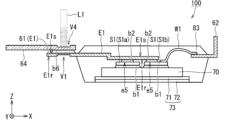
- FIG. 1 is a diagram for explaining a configuration of a semiconductor device according to a first embodiment
- FIG. 2 is a diagram for explaining a characteristic configuration of the first embodiment.
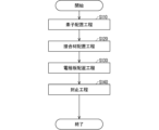
- 2 is a flowchart of a manufacturing method according to the first embodiment.
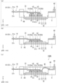
- 1A to 1C are cross-sectional views for explaining a manufacturing method according to the first embodiment.
- FIG. 11 is a cross-sectional view for explaining another embodiment of the joining method.
- FIG. 13 is a cross-sectional view showing another configuration of the recess.
- 11 is a diagram for explaining a configuration of a semiconductor device according to a second embodiment.
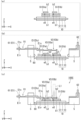
- FIG. 11A to 11C are cross-sectional views for explaining a manufacturing method according to a second embodiment.
- FIG. 11 is a cross-sectional view for explaining a configuration of a semiconductor device according to a third embodiment.
- FIG. 11 is a flowchart of a manufacturing method according to a third embodiment.
- 11A to 11C are cross-sectional views for explaining a manufacturing method according to a third embodiment.
- 13 is a cross-sectional view for explaining a configuration of a semiconductor device according to a fourth embodiment.
- FIG. 13 is a flowchart of a manufacturing method according to a fourth embodiment.
- 13A to 13C are cross-sectional views for explaining a manufacturing method according to a fourth embodiment.
- 13 is a block diagram showing a configuration of a power conversion system to which a power conversion device according to a fifth embodiment is applied.
- FIG. 11 is a flowchart of a manufacturing method according to a third embodiment.
- 11A to 11C are cross-sectional views for explaining a manufacturing method according to a third embodiment.
- 13 is a cross-sectional view for explaining a configuration of
- composition 1 is a diagram for explaining a configuration of a semiconductor device 100 according to a first embodiment.
- the semiconductor device 100 is, for example, a power module that operates at a high voltage.
- the semiconductor device 100 is not limited to a power module, and may be, for example, a semiconductor module that operates at a low voltage.
- FIG. 1(a) is a cross-sectional view of a semiconductor device 100 according to a first embodiment.
- FIG. 1(a) shows a terminal 64 (described below) that is not included in the semiconductor device 100.
- the X direction, Y direction, and Z direction are mutually orthogonal.
- the X direction, Y direction, and Z direction shown in the following figures are also mutually orthogonal.
- the direction including the X direction and the opposite direction of the X direction (-X direction) is also referred to as the "X-axis direction”.
- the direction including the Y direction and the opposite direction of the Y direction (-Y direction) is also referred to as the "Y-axis direction”.
- the direction including the Z direction and the opposite direction of the Z direction (-Z direction) is also referred to as the "Z-axis direction”.
- the plane including the X-axis direction and the Y-axis direction is also referred to as the "XY plane.”
- the plane including the X-axis direction and the Z-axis direction is also referred to as the "XZ plane.”
- the plane including the Y-axis direction and the Z-axis direction is also referred to as the "YZ plane.”
- FIG. 1(b) is a plan view of the semiconductor device 100 according to the first embodiment.
- the outline of the sealing resin 83 is shown by a dotted line in order to make it easier to understand the internal structure of the sealing resin 83, which will be described later.
- a terminal 64 is also shown in FIG. 1(b) in order to make it easier to understand the internal structure of the sealing resin 83, which will be described later.
- a terminal 64 is also shown in FIG. 1(b) and is not included in the semiconductor device 100.
- the semiconductor device 100 includes a heat spreader 70, a plurality of semiconductor elements S1, an insulating sheet 73, an electrode plate E1, a lead terminal 62, a wire W1, and a sealing resin 83.
- the heat spreader 70 is made of, for example, copper.
- the thickness of the heat spreader 70 is, for example, 2 mm.
- the shape of the heat spreader 70 in a plan view is rectangular.
- the size of the rectangle that is the shape of the heat spreader 70 is, for example, a size expressed as "25 mm x 40 mm.”
- a semiconductor element S1 is mounted on the upper surface of the heat spreader 70. Specifically, two adjacent semiconductor elements S1 are bonded to the upper surface of the heat spreader 70 via a bonding material b1.
- the joining material b1 is a thermosetting material.
- the joining material b1 is, for example, solder.
- the melting point of the solder that is the joining material b1 is, for example, 217°C.
- the solder is composed of tin, silver, and copper.
- the composition ratio of the solder that is the joining material b1 is expressed as "96.5% tin, 3% silver, 0.5% copper.”
- the semiconductor device 100 is provided with two heat spreaders 70. Therefore, the semiconductor device 100 includes a plurality of semiconductor elements S1, each of which has two adjacent semiconductor elements S1.
- Each of the multiple semiconductor elements S1 is, for example, a semiconductor chip. Each of the multiple semiconductor elements S1 has a plate shape. Each semiconductor element S1 is, for example, a power semiconductor element that operates at a high voltage. Note that each semiconductor element S1 is not limited to a power semiconductor element, and may be, for example, a semiconductor element that operates at a low voltage.
- Electrode e5 is provided on the top surface of each semiconductor element S1. That is, electrode e5 is an electrode provided on each semiconductor element S1. Electrode e5 is a main electrode. Electrode e5 is a conductive member having electrical conductivity.
- the semiconductor element S1a is, for example, a diode.
- the semiconductor element S1b is, for example, an IGBT (Insulated Gate Bipolar Transistor).
- the material constituting the semiconductor element S1a is, for example, silicon.
- the thickness of the semiconductor element S1a is, for example, 0.2 mm.
- the shape of the semiconductor element S1a in a plan view is rectangular.
- the size of the rectangle that is the shape of the semiconductor element S1a is, for example, a size expressed as "13 mm x 10 mm.”
- the material constituting the semiconductor element S1b is, for example, silicon.
- the thickness of the semiconductor element S1b is, for example, 0.2 mm.
- the shape of the semiconductor element S1b in a plan view is rectangular.
- the size of the rectangle that is the shape of the semiconductor element S1b is, for example, a size expressed as "13 mm x 13 mm.”
- the electrode plate E1 is made of, for example, copper.
- the thickness of the electrode plate E1 is, for example, 0.64 mm.
- the electrode plate E1 has one surface, the main surface E1s, and the other surface, the back surface E1r.
- the main surface E1s is the first surface.
- the back surface E1r is the second surface.
- the back surface E1r is the surface of the electrode plate E1 opposite the main surface E1s.
- FIG. 1(a) shows a curved electrode plate E1 as an example. Note that the electrode plate E1 does not have to be curved.
- the semiconductor device 100 operates using the electrode plate E1. That is, the semiconductor device 100 uses the electrode plate E1.
- the electrode e5 of the semiconductor element S1a and the electrode e5 of the semiconductor element S1b are connected to the electrode plate E1 via the bonding material b2. That is, the electrode plate E1 is electrically connected to the semiconductor element S1. This forms, for example, a main circuit.
- the bonding material b2 is in contact with the back surface E1r of the electrode plate E1 and the electrode e5 of the semiconductor element S1.
- the configuration of the bonding material b2 is the same as the configuration of the bonding material b1.
- the bonding material b2 has thermosetting properties.
- the bonding material b2 is, for example, solder.
- the material constituting the bonding material b2 is the same as the material constituting the bonding material b1.
- a signal electrode g1 is provided on the top surface of the semiconductor element S1b.
- the signal electrode g1 of the semiconductor element S1b is connected to a lead terminal 62 by a wire W1.
- the lead terminal 62 is a signal terminal.
- the lead terminal 62 is made of, for example, copper.
- the thickness of the lead terminal 62 is 0.64 mm.
- the wire W1 is made of, for example, aluminum.
- the thickness of the wire W1 is, for example, 0.15 mm.
- An insulating sheet 73 is disposed on the underside of the heat spreader 70.
- the insulating sheet 73 has a rectangular shape in a plan view.
- the size of the rectangular shape of the insulating sheet 73 is expressed as, for example, "62 mm x 44 mm.”
- the insulating sheet 73 is made of copper foil 72 and a thermally conductive resin layer 71.
- the thickness of the copper foil 72 is, for example, 0.1 mm.
- the thickness of the thermally conductive resin layer 71 is, for example, 0.05 mm.
- the thermally conductive resin layer 71 is provided on the copper foil 72.
- the sealing resin 83 is a resin that seals the multiple components included in the semiconductor device 100.
- the sealing resin 83 is produced by a transfer molding method.
- the sealing resin 83 is an epoxy resin in which silica filler has been dispersed.
- the sealing resin 83 mainly seals the insulating sheet 73, the heat spreader 70, the semiconductor elements S1, the electrode plate E1, the lead terminals 62, the wires W1, etc. A portion of the electrode plate E1 and a portion of the lead terminals 62 are exposed to the outside of the sealing resin 83.
- a part of the electrode plate E1 is a lead terminal 61.
- the lead terminal 61 is the electrode plate E1.
- the lead terminal 61 in the semiconductor device 100 is the part of the electrode plate E1 that is exposed to the outside of the sealing resin 83. Note that the entire electrode plate E1 may be the lead terminal 61.
- the lead terminal 61 which is the electrode plate E1, has a main surface E1s and a back surface E1r.
- the lead terminal 61 functions as an external terminal.
- the width of the lead terminal 61 is, for example, 10 mm.
- the semiconductor device 100 is provided with two heat spreaders 70 on which the semiconductor elements S1a and S1b are mounted.
- the semiconductor elements S1a and S1b mounted on the two heat spreaders 70 form two pairs of 2-in-1 modules.
- the number of electrode plates E1 provided on the semiconductor device 100 is, for example, three.
- the number of lead terminals 61 provided on the semiconductor device 100 is, for example, three.
- the number of electrode plates E1 provided on the semiconductor device 100 may be 1, 2, or 4 or more.
- the number of lead terminals 61 provided on the semiconductor device 100 may be 1, 2, or 4 or more.
- Fig. 2 is a diagram for explaining a characteristic configuration of the first embodiment.
- Fig. 2 is an enlarged view of the vicinity of a lead terminal 61 which is an electrode plate E1.
- the semiconductor device 100 is electrically connected to a terminal 64 of device A (not shown).
- the lead terminal 61 which is the electrode plate E1 is joined to the terminal 64 of device A.
- Device A is, for example, an external device.
- the external device is, for example, a device that operates using a semiconductor device.
- the external device is, for example, a transportation device such as an electric vehicle.
- Terminal 64 functions as an external terminal of device A.
- the terminal 64 of device A is a conductive member having electrical conductivity.
- the terminal 64 is made of, for example, copper.
- the thickness of the terminal 64 is, for example, 1 mm.
- the width of the terminal 64 is, for example, 12 mm.
- a recess V1 is formed on the main surface E1s of the lead terminal 61, which is the electrode plate E1.
- the recess V1 is formed in the lead terminal 61.
- the depth of the depression V1 is, for example, 0.3 mm.
- the shape of the depression V1 in a plan view is rectangular.
- the size of the rectangle that is the shape of the depression V1 is, for example, a size that can be expressed as "width 8 mm x 6 mm.”
- the recess V1 is away from the outer periphery of the main surface E1s of the lead terminal 61, which is the electrode plate E1. In other words, the recess V1 is away from the edge of the main surface E1s.
- the lead terminal 61 is joined to the terminal 64 of the device A via the bonding material b6.
- the back surface E1r of the lead terminal 61 which is the electrode plate E1
- the terminal 64 which is a conductive member
- the bonding material b6 is present between the lead terminal 61 and the terminal 64.
- the bonding material b6 is in contact with the back surface E1r of the lead terminal 61, which is the electrode plate E1, and with the terminal 64.
- the lead terminal 61, which is the electrode plate E1 is electrically connected to the terminal 64, which is a conductive member.
- the bonding material b6 is a thermosetting material.
- the configuration of the bonding material b6 is the same as the configuration of the bonding material b1.
- the bonding material b6 is, for example, solder.
- the material constituting the bonding material b6 is the same as the material constituting the bonding material b1.
- the recess V1 formed on the main surface E1s of the lead terminal 61, which is the electrode plate E1, is separated from the bonding material b6.
- state St1 the state of electrode plate E1 will also be referred to as "state St1."
- state St1 there exists a joining state Stc.
- the bonded state Stc includes a state St1a in which the back surface E1r of the electrode plate E1 is bonded to a conductive member via a bonding material.
- the bonding material is, for example, bonding material b6.
- the conductive member is, for example, a terminal 64.
- the electrode plate E1 in state St1a is, for example, the electrode plate E1 as a lead terminal 61 shown in Figures 1(a) and 2, etc.
- the bonding state Stc also includes a state St1b in which the recess V1 formed on the main surface E1s of the electrode plate E1 is separated from the bonding material.
- the bonding material in question is bonding material b6.
- the joining state Stc in this embodiment includes state St1a and state St1b.
- the electrode plate E1 in the joining state Stc is, for example, the electrode plate E1 as the lead terminal 61 shown in Figures 1(a) and 2, etc.
- laser light L1 emitted from, for example, a YAG laser is used to bond the lead terminal 61, which is the electrode plate E1.
- the depression V1 is the area onto which the laser light L1 is irradiated.
- the output of the YAG laser is, for example, 20 W.
- the wavelength of the laser light L1 is, for example, 1.064 nm.
- a recess V4 is formed in the terminal 64 of device A. Specifically, as shown in FIG. 1(a), the recess V4 is formed in the bottom surface of the terminal 64.
- the depth of the recess V4 is, for example, 0.5 mm.
- the shape of the recess V4 in a plan view is rectangular.
- the size of the rectangle that is the shape of the recess V4 is, for example, a size expressed as "width 8 mm x 6 mm".
- the recess V1 of the lead terminal 61 overlaps with the recess V4 of the terminal 64.
- FIG. 3 is a flowchart of the manufacturing method Pr according to the first embodiment. In Figure 3, only major steps included in the multiple steps of the manufacturing method Pr are shown.
- Figure 4 is a cross-sectional view for explaining the manufacturing method Pr according to the first embodiment.
- each of the semiconductor elements S1a and S1b will be explained as the semiconductor element S1.
- an initial process is first performed.
- a number of components used in manufacturing the semiconductor device 100 are prepared.
- the multiple components are shown in FIG. 4(a).
- the multiple components include a heat spreader 70, a lead frame 60, a semiconductor element S1, bonding materials b1 and b2, a lead terminal 62, and an electrode plate E1.
- Each of the prepared bonding materials b1 and b2 has a plate shape.
- An electrode plate E1 and a lead terminal 62 are connected to the lead frame frame 60.
- the electrode plate E1 connected to the lead frame frame 60 is a member in which a part of the electrode plate E1 becomes the lead terminal 61 in a process described below.
- a recess V1 is formed in advance on the main surface E1s of the electrode plate E1.
- the recess V1 is formed, for example, by etching or the like.
- step S110 the element placement process is performed (step S110).
- the semiconductor element S1 is placed on the upper surface of the heat spreader 70 via a plate-shaped bonding material b1.
- the bonding material placement process is a process in which bonding material b2 is placed on the upper surface of a conductive member.
- the bonding material b2 has thermosetting properties.
- the conductive member in question is the electrode e5 provided on the upper surface of the semiconductor element S1.
- the conductive member in question is the electrode e5 provided on the semiconductor element S1.
- a plate-shaped bonding material b2 is placed on the upper surface of the electrode e5 of the semiconductor element S1.
- the electrode plate arrangement process is a process in which the electrode plate E1 is arranged on the bonding material b2 so that the back surface E1r of the electrode plate E1 contacts the bonding material b2.
- the electrode plate E1 is arranged on the bonding material b2 so that the back surface E1r of the electrode plate E1 contacts the bonding material b2.
- the heating step N is performed.
- the bonding materials b1 and b2 are heated. Specifically, the bonding materials b1 and b2 are heated so that they melt.
- the bonding materials b1 and b2 are heated using a reflow furnace.
- the bonding materials b1 and b2 are heated so that the temperature of the bonding materials b1 and b2 rises to 280°C.
- the semiconductor element S1 is bonded to the upper surface of the heat spreader 70 by the bonding material b1.
- the electrode plate E1 is also bonded to the electrode e5 of the semiconductor element S1.
- the terminal connection process is performed.
- the lead terminal 62 is electrically connected to the signal electrode g1 (not shown) of the semiconductor element S1b as the semiconductor element S1 by the wire W1 (see FIG. 4(b)).
- an insulating sheet 73 is attached to the underside of the heat spreader 70.
- step S140 the sealing process is performed (step S140).
- a transfer molding method is performed so that multiple components are sealed in the sealing resin 83.
- the multiple components are the insulating sheet 73, the heat spreader 70, the semiconductor element S1, the electrode plate E1, the lead terminal 62, the wire W1, etc.
- the frame removal process is performed.
- the lead frame 60 is removed.
- the lead forming process is performed.
- pressure is applied to the lead terminal 62 so that the lead terminal 62 is bent.
- the above steps result in the semiconductor device 100 shown in FIG. 4(c).
- the portion of the electrode plate E1 that is exposed to the outside of the sealing resin 83 is the lead terminal 61.
- the joining method Pc of the present embodiment is a method of joining the lead terminal 61, which is the electrode plate E1 included in the semiconductor device 100 of FIG. 4C, to the terminal 64 (i.e., the conductive member) of the device A.
- the joining process N is a process of irradiating a laser beam L1 to a recess V1 formed on the main surface E1s of the electrode plate E1 so that the state of the electrode plate E1 becomes the above-mentioned joined state Stc.
- the joining state Stc of this embodiment includes state St1a and state St1b.
- State St1a of this embodiment is a state in which the back surface E1r of the electrode plate E1 is joined to the terminal 64, which is a conductive member, via the joining material b6.
- State St1b of this embodiment is a state in which the recess V1 formed on the main surface E1s of the electrode plate E1 is separated from the joining material b6.
- a plate-shaped joining material b6 is placed on the upper surface of the terminal 64, which is a conductive member.
- the lead terminal 61 which is the electrode plate E1 is positioned so that the recess V1 of the lead terminal 61 overlaps the bonding material b6 in a plan view.
- irradiation process A is performed.
- laser light L1 is irradiated onto the bottom of the recess V1.
- the irradiation of laser light L1 is also referred to as "laser light irradiation.”
- the laser light irradiation of joining method Pc is the irradiation of the laser light L1 onto the bottom of the recess V1.
- the bonding material b6 is heated by laser light irradiation so that the bonding material b6 melts.
- the bonding material b6 is heated so that the bonding material b6 melts due to heat generated in the lead terminal 61, which is the electrode plate E1, by the laser light irradiation.
- the heating of the bonding material b6 i.e., the laser light irradiation
- the bonding material b6 hardens again.
- the recess V1 is formed on the main surface E1s of the electrode plate E1. Therefore, the heat capacity of the electrode plate E1 can be reduced. As a result, for example, in a situation where the electrode plate E1 is heated by irradiating the recess V1 of the electrode plate E1 with the laser light L1, the heat of the electrode plate E1 can be efficiently transferred to the bonding material b6. Therefore, the electrode plate E1 is firmly bonded to the terminal 64, which is a conductive member, via the bonding material b6 having thermosetting properties.
- the depression V1 formed on the main surface E1s of the electrode plate E1 is separated from the bonding material b6. Therefore, even if, for example, laser light L1 is irradiated onto the depression V1 on the main surface E1s of the electrode plate E1 in order to heat the electrode plate E1, the following problem can be prevented from occurring. For example, the problem is that the laser light L1 is directly irradiated onto the bonding material b6, causing the bonding material b6 to scatter.
- a recess V1 is formed on the main surface E1s of the lead terminal 61, which is the electrode plate E1.
- laser light L1 is irradiated onto the bottom of the recess V1 so that the bonding material b6 in contact with the back surface E1r of the lead terminal 61 melts.
- the recess V1 is formed in the lead terminal 61, which is the electrode plate E1
- the thickness of the portion of the lead terminal 61 where the recess V1 exists is thin.
- the heat capacity of the lead terminal 61 is smaller than the heat capacity of a lead terminal that does not have the recess V1. This makes it possible to increase the thermal conductivity of the lead terminal 61.
- the lead terminal 61 has the property that the temperature of the lead terminal 61 easily increases.
- the thermal conduction to the rear surface E1r of the lead terminal 61 can be improved.
- the recess V1 is located away from the outer periphery of the main surface E1s of the lead terminal 61. This makes it possible to prevent the following problem from occurring. For example, the problem is that the solder, which is the joining material b6, flows up to the recess V1 and is then irradiated with laser light, causing the solder to splash.
- a recess V1 is formed in the lead terminal 61, which is the electrode plate E1. Furthermore, the lead terminal 61 is joined to the terminal 64 of the device A via the joining material b6.
- the lead terminal 61 is joined by irradiating the portion of the lead terminal 61 that is to be joined to the terminal 64 with laser light.
- the joining of the lead terminal 61 can be achieved by localized irradiation with laser light. Therefore, by irradiating the lead terminal 61 with laser light, the range to which the heat generated in the lead terminal 61 is transferred can be limited.
- a recess V4 is formed on the underside of the terminal 64. This reduces the thermal capacity of the terminal 64. In addition, it is possible to improve thermal conduction to the bonding material b6 sandwiched between the lead terminal 61 and the terminal 64.
- connection method that is often used is soldering.
- lead frames have excellent thermal conductivity, the following problem is likely to occur. This problem is that heat spreads over a wide area in the lead frame. When this problem occurs, the temperature of the parts to be joined does not rise sufficiently, resulting in insufficient soldering.
- the heat input to the lead frame is excessively large, the heat is transferred through the lead frame, which can easily cause the following problems.
- the solder inside the module melts, affecting the reliability of the joints.
- the solder expands, causing cracks in the sealing resin.
- the problem in question is that when the solder that has become wet is directly irradiated with laser light, the solder with a low melting point scatters into the surrounding area. When this problem occurs, problems such as short circuits and reduced insulation can occur.
- the semiconductor device 100 of this embodiment has a configuration for achieving the above-mentioned effects. Therefore, the semiconductor device 100 of this embodiment can solve the above-mentioned problems.
- SiC semiconductor elements made of silicon carbide (SiC) have a high operating temperature and excellent power conversion efficiency. For this reason, SiC semiconductor elements have become mainstream semiconductor elements in recent years. Therefore, there is a demand for power modules that can accommodate SiC semiconductor elements.
- the semiconductor device 100 of this embodiment has a configuration for achieving the above-mentioned effects. Therefore, it is possible to apply a SiC semiconductor element as the semiconductor element S1 mounted on the semiconductor device 100.
- the terminal 64 of the device A is joined to the back surface E1r of the lead terminal 61, which is the electrode plate E1, but this is not limited to this.
- a configuration may be used in which a terminal 64 is bonded to the main surface E1s of the lead terminal 61.
- a recess V4 is formed on the upper surface of the terminal 64
- a recess V1 is formed on the rear surface E1r of the lead terminal 61.
- laser light is irradiated onto the recess V4 of the terminal 64. This provides the same effect as the bonding method Pc of embodiment 1.
- configuration Cs1 the configuration in which the shape of the depression in a plan view is rectangular is also referred to as “configuration Cs1."
- Depression V1 in configuration Cs1 is, for example, depression V1 in FIG. 2.
- FIG. 6 is a cross-sectional view showing another configuration of the recess V1.
- the depression V1 may be composed of multiple grooves V1a.
- a configuration in which a depression is composed of multiple grooves V1a is also referred to as "configuration Cs2.”
- a depression V1 to which configuration Cs2 is applied is composed of multiple grooves V1a.
- each groove V1a is linear.
- the depth of each groove V1a is, for example, 0.3 mm.
- the shape of each groove V1a in a plan view is rectangular.
- the size of the rectangle that is the shape of each groove V1a is, for example, a size expressed as "width 8 mm x 1.2 mm.”
- configuration Cs2 can suppress the decrease in rigidity of electrode plate E1 more than configuration Cs1. This has the effect of making it easier to ensure the flatness of electrode plate E1.
- shape of each groove V1a is not limited to a straight line, and may be, for example, a square shape.
- configuration Cs3 the configuration in which the cross-sectional shape of the depression along the depth direction of the depression is triangular.
- the depression V1 to which the configuration Cs3 is applied is a groove.
- the shape of the depression V1 is linear. Also, as shown in FIG. 6(b), multiple depressions V1 to which the configuration Cs3 is applied may be formed.
- the shape of the depression V1 in FIG. 6(b) is rectangular.
- the size of the rectangle that is the shape of the depression V1, which is a groove, is expressed as, for example, "width 8 mm x 1.2 mm.”
- the laser light L1 is diffusely reflected in the above-mentioned irradiation process A. This makes it possible to reduce the reflectance of the laser light L1 on the electrode plate E1. This makes it possible to more reliably increase the temperature of the electrode plate E1 in the irradiation process A.
- the shape of the depression V1 in configuration Cs3 is not limited to a straight line and may be, for example, a square shape.
- the shape of the depression V1 can be made into a plurality of cylinders or cones to ensure diffuse reflection of the laser light L1.
- the most efficient way to increase the absorption rate is to have a diameter of the cylinders or cones that is approximately 1x the fiber diameter or spot diameter of the laser light L1. Furthermore, the deeper the cylinders or cones are, the more likely they are to cause diffuse reflection. It is desirable for the aspect ratio of depth/diameter to be 0.5 or greater.
- a through hole may be provided in part of the bottom of the recess V1.
- this structure is a structure in which solder does not wet up in the through hole.
- this structure is a structure in which the inner wall of the through hole, the periphery of the through hole, etc. are coated with a resin that does not cause solder wettability.
- this structure is a structure in which the inner wall of the through hole, the periphery of the through hole, etc. are plated with a metal that does not easily cause solder wettability.
- the material constituting the electrode plate E1, heat spreader 70, etc. is not limited to copper.
- the material constituting the electrode plate E1, heat spreader 70, etc. may be, for example, a copper alloy.
- the material constituting the electrode plate E1, heat spreader 70, etc. may be, for example, aluminum with nickel plating on the surface of the aluminum.
- the material constituting the semiconductor element S1 is not limited to silicon.
- the material constituting the semiconductor element S1 may be, for example, a wide bandgap semiconductor material such as silicon carbide, silicon carbide (SiC), gallium nitride, diamond, etc.
- a wide bandgap semiconductor material is a material that has a bandgap wider than that of silicon.
- the composition ratio of the solder of the joining materials b1, b2, b6, etc. is expressed as "96.5% tin, 3% silver, 0.5% copper" and the melting point of the solder is 217°C, but this is not limited to this.
- the composition ratio of the solder of the joining materials b1, b2, b6, etc. may be expressed as "99.3% tin, 0.7% copper” and the melting point of the solder may be 224°C.
- the bonding materials b1, b2, b6, etc. are not limited to solder.
- the bonding materials b1, b2, b6, etc. may be materials that have better heat resistance than solder.
- the bonding materials b1, b2, b6, etc. may be, for example, a silver sintered material, a brazing material, etc.
- the material constituting the wire W1 is not limited to aluminum.
- the material constituting the wire W1 may be, for example, an aluminum alloy, copper, etc.
- the aluminum alloy contains a small amount of additive.
- the additive is, for example, iron.
- the sealing resin 83 is not limited to the epoxy resin in which a silica filler is dispersed.
- the sealing resin 83 may be, for example, the epoxy resin in which a filler such as alumina is dispersed.
- the sealing resin 83 may be, for example, the epoxy resin in which a silicone resin is mixed into the epoxy resin.
- terminal 64 of device A is described as having a recess V4 formed therein, this is not limited to the above.
- the terminal 64 of device A does not necessarily have to have a recess V4 formed therein.
- compositions 7A and 7B are diagrams for explaining the configuration of a semiconductor device 100A according to a second embodiment.
- Fig. 7A is a cross-sectional view of the semiconductor device 100A according to the second embodiment.
- Fig. 7A shows a terminal 64 of the device A described above, which is not included in the semiconductor device 100A.
- Fig. 7B is a plan view of the semiconductor device 100A according to the first embodiment.
- Fig. 7B shows a terminal 64 that is not included in the semiconductor device 100A.
- the semiconductor device 100A differs in that it has a sealing material 84 instead of the sealing resin 83, has an insulating substrate 10 instead of the heat spreader 70, further has a case 5, and does not have an insulating sheet 73.
- the rest of the configuration of the semiconductor device 100A is the same as that of the semiconductor device 100. Below, the differences between the semiconductor device 100A and the semiconductor device 100 will be mainly described.
- the shape of the case 5 is, for example, cylindrical. Also, the shape of the case 5 in a plan view is a closed loop.
- the case 5 is made of, for example, PPS (Poly Phenylene Sulfide) resin.
- the electrode plate E1 and the lead terminal 62 are fixed to the case 5 by insert molding.
- the electrode plate E1 and the lead terminal 62 are integrated with the case 5.
- the electrode plate E1 is made of, for example, copper.
- the thickness of the electrode plate E1 is, for example, 0.64 mm.
- the outline shape of the case 5 in a plan view is, for example, rectangular.
- the case 5 houses multiple components included in the semiconductor device 100A.
- the multiple components are the insulating substrate 10, multiple semiconductor elements S1, electrode plate E1, wires W1, etc.
- the case 5 houses at least the semiconductor element S1.
- the case 5 is joined to the insulating substrate 10 by adhesive 80.
- the insulating substrate 10 is a substrate having insulating properties.
- the insulating substrate 10 is, for example, a ceramic substrate.
- the insulating substrate 10 includes a base material 11, a plurality of conductor layers 12, and a conductor layer 13.
- the base material 11 is made of, for example, aluminum nitride.
- the shape of the base material 11 is a plate.
- the thickness of the base material 11 is, for example, 2 mm.
- the shape of the base material 11 in a plan view is rectangular.
- the size of the rectangle that is the shape of the base material 11 is, for example, a size expressed as "40 mm x 40 mm".
- Each conductor layer 12 is made of, for example, copper.
- the thickness of each conductor layer 12 is, for example, 0.8 mm.
- the shape of the conductor layer 12 in a plan view is rectangular.
- the size of the rectangle that is the shape of the conductor layer 12 is, for example, expressed as "17 mm x 37 mm.”
- a conductor layer 13 is formed on the lower surface of the substrate 11.
- the conductor layer 13 is made of, for example, copper.
- the thickness of the conductor layer 13 is, for example, 0.8 mm.
- the shape of the conductor layer 13 in a plan view is rectangular.
- the size of the rectangle that is the shape of the conductor layer 13 is, for example, expressed as "37 mm x 37 mm.”
- a semiconductor element S1 is mounted on the insulating substrate 10. Specifically, semiconductor elements S1a and S1b, which are the semiconductor element S1, are mounted on each conductor layer 12 of the insulating substrate 10 by means of a bonding material b1.
- the semiconductor device 100A operates using the electrode plate E1. That is, the semiconductor device 100A uses the electrode plate E1.
- the electrode e5 of the semiconductor element S1a and the electrode e5 of the semiconductor element S1b are connected to the electrode plate E1 via the bonding material b2.
- the electrode plate E1 is electrically connected to the semiconductor element S1.
- the bonding material b2 is in contact with the back surface E1r of the electrode plate E1 and the electrode e5 of the semiconductor element S1.
- the signal electrode g1 of the semiconductor element S1b is connected to the lead terminal 62 by the wire W1.
- a sealant 84 is provided inside the case 5.
- the sealant 84 is, for example, a silicone gel.
- the sealant 84 mainly seals the insulating substrate 10, the semiconductor elements S1, the electrode plate E1, the wires W1, etc.
- a part of the electrode plate E1 in the semiconductor device 100A is a lead terminal 61. That is, the lead terminal 61 is the electrode plate E1.
- the lead terminal 61 in the semiconductor device 100A is the part of the electrode plate E1 that is exposed to the outside of the case 5. Note that the entire electrode plate E1 may be the lead terminal 61.
- the lead terminal 61, which is the electrode plate E1, has a main surface E1s and a back surface E1r.
- the semiconductor device 100A is electrically connected to a terminal 64 of device A (not shown). Specifically, the lead terminal 61, which is the electrode plate E1, is joined to the terminal 64 of device A.
- a recess V1 is formed on the main surface E1s of the lead terminal 61, which is the electrode plate E1. In other words, the recess V1 is formed in the lead terminal 61.
- the configuration of the recess V1 in this embodiment is similar to the configuration of the recess V1 in embodiment 1.
- the shape of the recess V1 in a plan view is rectangular.
- the recess V1 is located away from the outer periphery of the main surface E1s of the lead terminal 61, which is the electrode plate E1. In other words, the recess V1 is located away from the edge of the main surface E1s.
- the lead terminal 61 is joined to the terminal 64 of the device A via the bonding material b6. Specifically, the back surface E1r of the lead terminal 61, which is the electrode plate E1, is joined to the terminal 64, which is a conductive member, via the bonding material b6. In other words, the lead terminal 61, which is the electrode plate E1, is electrically connected to the terminal 64, which is a conductive member.
- the bonding material b6 is a thermosetting material.
- the configuration of the bonding material b6 is the same as that of the bonding material b1.
- the bonding material b6 is, for example, solder.
- the depression V1 formed on the main surface E1s is separated from the bonding material b6.
- a recess V4 is formed in terminal 64 of device A.
- FIG. 8 is a cross-sectional view for explaining the manufacturing method Pra according to the second embodiment.
- the manufacturing method Pra of the semiconductor device 100A will be described, focusing mainly on the differences from the manufacturing method Pr of FIG. 3 in the first embodiment.
- each of the semiconductor elements S1a and S1b will be described as the semiconductor element S1.
- an initial process A is carried out first.
- a number of components used in the manufacture of the semiconductor device 100A are prepared.
- the multiple components are shown in FIG. 8(a).
- the multiple components include the case 5, the insulating substrate 10, the semiconductor element S1, the bonding materials b1 and b2, the lead terminal 62, the electrode plate E1, etc.
- Each of the prepared bonding materials b1 and b2 has a plate shape.
- step S110 an element placement process is performed (step S110).
- a semiconductor element S1 is placed on the upper surface of the conductor layer 12 of the insulating substrate 10 via a plate-shaped bonding material b1.
- the heating step A1 is performed.
- the bonding material b1 is heated so that the bonding material b1 melts.
- the bonding material b1 is heated using a reflow furnace.
- the bonding material b1 is heated so that the temperature of the bonding material b1 rises to 280°C.
- the semiconductor element S1 is bonded to the upper surface of the conductor layer 12 of the insulating substrate 10 by the bonding material b1.
- a bonding material placement step is performed (step S120).
- a thermosetting bonding material b2 is placed on the upper surface of the conductive member.
- the conductive member in question is the electrode e5 provided on the upper surface of the semiconductor element S1.
- the insert molding process is performed.
- the electrode plate E1 and the lead terminal 62 are fixed to the case 5 by insert molding.
- the part of the electrode plate E1 that is exposed to the outside of the case 5 is the lead terminal 61.
- the timing of the insert molding process is not limited to the timing after the bonding material placement process.
- the insert molding process may be performed in parallel with the element placement process, for example.
- the heating step A2 is performed.
- the bonding material b2 is heated so that the bonding material b2 melts.
- the heating step A2 may be performed after the electrode plate arrangement step described below.
- the electrode plate E1 is arranged on the bonding material b2 so that the back surface E1r of the electrode plate E1 contacts the bonding material b2. This causes the electrode plate E1 to be bonded to the electrode e5 of the semiconductor element S1 (see FIG. 8(b)).
- the case joining process is a process in which the case 5 is joined to the insulating substrate 10 via adhesive 80.
- the case 5 which has adhesive 80 applied to its inner surface as shown in FIG. 8(a), is joined to the insulating substrate 10 via the adhesive 80 (see FIG. 8(b)).
- the terminal connection process is performed as in the first embodiment.
- the lead terminal 62 fixed to the case 5 is electrically connected to the signal electrode g1 (not shown) of the semiconductor element S1b as the semiconductor element S1 by the wire W1.
- the sealing process F is performed.
- a fluid sealing material 84 is injected into the case 5.
- the sealing material 84 then hardens.
- multiple components are sealed within the sealing material 84.
- the multiple components are the insulating substrate 10, the semiconductor element S1, the lead terminals 62, the electrode plate E1, the wire W1, etc.
- the bonding method Pc of the present embodiment is a method for bonding a lead terminal 61, which is an electrode plate E1 included in the semiconductor device 100A of FIG. 8C, to a terminal 64 (i.e., a conductive member) of the device A.
- a joining step N is performed in the same manner as in the first embodiment.
- a laser beam L1 is irradiated onto a recess V1 formed on the main surface E1s of the electrode plate E1 so that the state of the electrode plate E1 becomes the aforementioned joined state Stc.
- the back surface E1r of the lead terminal 61 which is the electrode plate E1 is joined to the terminal 64, which is a conductive member, via the joining material b6.
- the semiconductor device 100A using the case 5 has the same effects as those of the first embodiment.
- a semiconductor device having high reliability can be provided.
- the solderability of the lead terminals 61 can be improved.
- Fig. 9 is a cross-sectional view for explaining the configuration of a semiconductor device 100B according to the third embodiment.
- Fig. 9 shows a terminal 64 of the device A described above, which is not included in the semiconductor device 100B.
- the two electrode plates E1 joined together by the bonding material are also referred to as "joined electrode plates.”
- the shape of the joined electrode plate in this embodiment is similar to the shape of the electrode plate E1 in the semiconductor device 100A in FIG. 7(a), for example.
- the size of the joined electrode plate in this embodiment is equivalent to the size of the electrode plate E1 in the semiconductor device 100A.
- the bonded electrode plate includes two electrode plates E1 bonded to each other.
- Each electrode plate E1 included in the bonded electrode plate has a main surface E1s and a back surface E1r.
- Each electrode plate E1 included in the bonded electrode plate is made of, for example, copper.
- the size of each electrode plate E1 included in the bonded electrode plate is smaller than the size of the electrode plate E1 included in the semiconductor device 100A.
- each of the electrode plates E1a and E1b is a conductive member.
- Each of the electrode plates E1a and E1b has a plate-like shape.
- the electrode plates E1a and E1b are not bent.
- the size of each of the electrode plates E1a and E1b is smaller than the size of the electrode plate E1 included in the semiconductor device 100A.
- the semiconductor device 100B differs in that a bonding electrode plate is used instead of the electrode plate E1 of the semiconductor device 100A.
- the semiconductor device 100B has a configuration that uses a bonding electrode plate.
- the rest of the configuration of the semiconductor device 100B is similar to that of the semiconductor device 100A. Below, the semiconductor device 100B will be described, focusing mainly on the differences from the semiconductor device 100A.
- the electrode plate E1a is joined to the electrode plate E1b, which is a conductive member, via the bonding material b3.
- the bonded electrode plate is formed by bonding the electrode plate E1a to the electrode plate E1b via the bonding material b3.
- Electrode plate E1a is electrically connected to electrode plate E1b. Specifically, the back surface E1r of electrode plate E1a is joined to electrode plate E1b via bonding material b3. Bonding material b3 is in contact with the back surface E1r of electrode plate E1a and electrode plate E1b.
- the configuration of the bonding material b3 is the same as the configuration of the bonding material b1.
- the bonding material b3 has thermosetting properties.
- the bonding material b3 is, for example, solder.
- the material constituting the bonding material b3 is the same as the material constituting the bonding material b1.
- the electrode plate E1a and the lead terminal 62 are fixed to the case 5 by insert molding.
- the electrode plate E1a and the lead terminal 62 are integrated with the case 5.
- the case 5 houses multiple components included in the semiconductor device 100B.
- the multiple components are the insulating substrate 10, multiple semiconductor elements S1, electrode plates E1a and E1b, wires W1, etc.
- the case 5 houses at least the semiconductor element S1.
- Semiconductor elements S1a and S1b which are semiconductor elements S1, are mounted on each conductor layer 12 of the insulating substrate 10 of the semiconductor device 100B using a bonding material b1.
- the semiconductor device 100B operates using electrode plates E1a and E1b, which are electrode plate E1. In other words, the semiconductor device 100B uses electrode plates E1a and E1b.
- electrode e5 of semiconductor element S1a and electrode e5 of semiconductor element S1b are connected to electrode plate E1b via bonding material b2. That is, electrode plate E1b is bonded to semiconductor element S1. That is, electrode plate E1b is electrically connected to semiconductor element S1. Bonding material b2 is in contact with the back surface E1r of electrode plate E1b and electrode e5 of semiconductor element S1.
- electrode plate E1a is electrically connected to electrode plate E1b. Therefore, electrode plate E1a is electrically connected to semiconductor element S1.
- the signal electrode g1 of the semiconductor element S1b is connected to the lead terminal 62 by the wire W1.
- the sealing material 84 mainly seals the insulating substrate 10, the multiple semiconductor elements S1, the electrode plates E1a and E1b, the wires W1, etc.
- a part of the electrode plate E1a in the semiconductor device 100B is a lead terminal 61. That is, the lead terminal 61 is the electrode plate E1a as the electrode plate E1.
- the lead terminal 61 in the semiconductor device 100B is the part of the electrode plate E1a that is the electrode plate E1 that is exposed to the outside of the case 5. Note that the entire electrode plate E1a may be the lead terminal 61.
- the lead terminal 61 that is the electrode plate E1a as the electrode plate E1 has a main surface E1s and a back surface E1r.
- the semiconductor device 100B is electrically connected to a terminal 64 of device A (not shown). Specifically, the lead terminal 61, which is the electrode plate E1a, is joined to the terminal 64 of device A.
- a recess V1 is formed on the main surface E1s of the lead terminal 61, which is the electrode plate E1a. In other words, the recess V1 is formed in the lead terminal 61.
- the configuration of the recess V1 in this embodiment is similar to the configuration of the recess V1 in embodiment 1.
- the shape of the recess V1 in a plan view is rectangular.
- electrode junction the portion of electrode plate E1a that is joined to electrode plate E1b is also referred to as the "electrode junction.”
- the electrode junction is the end of electrode plate E1a.
- a recess V2 is formed in the electrode junction of electrode plate E1a.
- a recess V2 is formed in the main surface E1s of the electrode junction of electrode plate E1a. That is, recess V1 and recess V2 are formed in the main surface E1s of electrode plate E1a.
- the configuration of the recess V2 is the same as the configuration of the recess V1.
- the depth of the recess V2 is, for example, 0.3 mm.
- the shape of the recess V2 in a plan view is rectangular.
- the size of the rectangle that is the shape of the recess V2 is, for example, a size expressed as "width 8 mm x 6 mm.”
- the recess V2 is away from the outer periphery of the main surface E1s of the electrode plate E1a. In other words, the recess V2 is away from the edge of the main surface E1s.
- FIG. 10 is a flowchart of manufacturing method Prb according to embodiment 3.
- FIG. 10 shows only the main steps included in the multiple steps of manufacturing method Prb.
- FIG. 11 is a cross-sectional view for explaining manufacturing method Prb according to embodiment 3.
- the manufacturing method Prb of the semiconductor device 100B will be described, focusing mainly on the differences from the manufacturing method Pra in the second embodiment.
- each of the semiconductor elements S1a and S1b will be described as the semiconductor element S1.
- an initial process B is performed first.
- a plurality of components to be used in manufacturing the semiconductor device 100B are prepared.
- FIG. 11(a) shows some of the plurality of components.
- the plurality of components include an insulating substrate 10, a semiconductor element S1, bonding materials b1 and b2, and an electrode plate E1b.
- Each of the prepared bonding materials b1 and b2 has a plate shape.
- FIG. 11(b) shows the case 5, the lead terminal 62, the electrode plate E1a, etc. as another part of the multiple members to be prepared.
- the main surface E1s of the electrode plate E1a to be prepared has recesses V1 and V2 formed in advance.
- step S110 an element placement process is performed (step S110).
- a semiconductor element S1 is placed on the upper surface of the conductor layer 12 of the insulating substrate 10 via a plate-shaped bonding material b1.
- the bonding material placement process is a process of placing a bonding material b2 on the upper surface of a conductive member.
- the bonding material b2 has thermosetting properties.
- the conductive member is an electrode e5 provided on the upper surface of the semiconductor element S1.
- a plate-shaped bonding material b2 is placed on the upper surface of the electrode e5 of the semiconductor element S1.
- the electrode plate arrangement process B is a process of arranging the electrode plate E1b, which is the electrode plate E1, on the bonding material b2 so that the back surface E1r of the electrode plate E1b contacts the bonding material b2.
- the electrode plate E1b is arranged on the bonding material b2 so that the back surface E1r of the electrode plate E1b contacts the bonding material b2.
- the heating step N is performed in the same manner as in the first embodiment.
- the bonding materials b1 and b2 are heated so that they melt.
- the semiconductor element S1 is bonded to the upper surface of the conductor layer 12 of the insulating substrate 10 by the bonding material b1 (see FIG. 11(b)).
- the electrode plate E1b is bonded to the electrode e5 of the semiconductor element S1. That is, the electrode plate E1b is bonded to the semiconductor element S1.
- the insert molding process B is performed.
- the electrode plate E1a and the lead terminal 62 are fixed to the case 5 by insert molding (see FIG. 11(b)).
- the part of the electrode plate E1a, which is the electrode plate E1 that is exposed to the outside of the case 5 is the lead terminal 61.
- the timing of the insert molding process B is not limited to the timing after the electrode plate arrangement process B.
- the insert molding process B may be performed in parallel with the element arrangement process, for example.
- the bonding material placement process B is a process of placing a bonding material b3 on the upper surface of a conductive member.
- the bonding material b3 has thermosetting properties.
- the conductive member is an electrode plate E1b that is bonded to the semiconductor element S1.
- a plate-shaped bonding material b3 is placed on the main surface E1s, which is the upper surface of the electrode plate E1b.
- step S132B the electrode plate arrangement process Ba is performed (step S132B).
- the case joining process is performed in parallel with the electrode plate arrangement process Ba.
- the electrode plate arrangement process Ba is a process of arranging the electrode plate E1a, which is the electrode plate E1, on the bonding material b3 so that the back surface E1r of the electrode plate E1a contacts the bonding material b3.
- the electrode plate E1a is an electrode that is fixed to the case 5 by the insert molding process B described above.
- the electrode plate E1a is arranged on the bonding material b3 so that the back surface E1r of the electrode plate E1a contacts the bonding material b3.
- the electrode plate E1a is arranged so that the recess V2 of the electrode plate E1a overlaps with the bonding material b3 in a plan view.
- the bonding material b3 is sandwiched between the electrode plates E1a and E1b.
- the case 5 which has adhesive 80 applied to its inner surface as shown in FIG. 11(b), is joined to the insulating substrate 10 via the adhesive 80 (see FIG. 11(c)).
- the joining process B is a process of irradiating the laser light L1 to the recess V2 formed on the main surface E1s of the electrode plate E1a so that the state of the electrode plate E1a becomes the above-mentioned joined state Stc.
- the joining state Stc in this embodiment includes state St1a and state St1b.
- State St1a in this embodiment is a state in which the back surface E1r of the electrode plate E1a is joined to the electrode plate E1b, which is a conductive member, via the joining material b3.
- State St1b in this embodiment is a state in which the recess V2 formed on the main surface E1s of the electrode plate E1a is separated from the joining material b3.
- an irradiation process B is performed.
- the bottom of the recess V2 is irradiated with laser light L1.
- the irradiation of the laser light L1 is also called “laser light irradiation.”
- the laser light irradiation in the manufacturing method Prb is the irradiation of the laser light L1 to the bottom of the recess V2.
- the bonding material b3 is heated by laser light irradiation so that the bonding material b3 melts.
- the heating of the bonding material b3 is performed so that the bonding material b3 melts due to heat generated in the electrode plate E1a by the laser light irradiation.
- the heating of the bonding material b3 i.e., the laser light irradiation
- the bonding material b3 hardens again.
- the terminal connection process is carried out in the same manner as in the second embodiment.
- the lead terminal 62 fixed to the case 5 is electrically connected to the signal electrode g1 (not shown) of the semiconductor element S1b as the semiconductor element S1 by the wire W1 (see FIG. 9).
- sealing process F is performed (step S140B).
- sealing material 84 having fluidity is injected into case 5.
- sealing material 84 hardens. As a result, multiple components are sealed within sealing material 84.
- the bonding method Pc of the present embodiment is a method for bonding a lead terminal 61, which is an electrode plate E1a included in the semiconductor device 100B of FIG.
- a joining step N is performed in the same manner as in the second embodiment.
- a laser beam L1 is irradiated onto a recess V1 formed on the main surface E1s of the electrode plate E1a, which is the electrode plate E1, so that the state of the electrode plate E1a becomes the joining state Stc described above.
- the back surface E1r of the lead terminal 61 which is the electrode plate E1a (i.e., the electrode plate E1), is joined to the terminal 64, which is a conductive member, via the joining material b6.
- the semiconductor device 100B can achieve the same effects as those of the first embodiment.
- the semiconductor device 100B also has a configuration using a bonding electrode plate.
- the bonding electrode plate is formed by bonding an electrode plate E1a to an electrode plate E1b via a bonding material b3.
- the electrode plate E1a is fixed to the case 5 by insert molding.
- the electrode plate E1b is bonded to the semiconductor element S1 mounted on the insulating substrate 10.
- Fig. 12 is a cross-sectional view for explaining the configuration of a semiconductor device 100C according to the fourth embodiment.
- Fig. 12 shows a terminal 64 of the device A described above, which is not included in the semiconductor device 100C.
- the semiconductor device 100C differs in that multiple recesses are formed in the electrode plate E1. Other than that, the configuration of the semiconductor device 100C is the same as that of the semiconductor device 100A. Below, the semiconductor device 100C will be described, focusing mainly on the differences from the semiconductor device 100A.
- the electrode plate E1 included in the semiconductor device 100C will also be referred to as “electrode plate E1c.”
- the electrode plate E1c has a main surface E1s and a back surface E1r.
- the electrode plate E1c is curved. Note that the electrode plate E1c does not have to be curved.
- the electrode plate E1c differs from the electrode plate E1 in FIG. 7(a) in that a recess V3 is further formed on the main surface E1s.
- the rest of the configuration of the electrode plate E1c is the same as that of the electrode plate E1 in FIG. 7(a).
- Two recesses V3 are formed on the main surface E1s of the electrode plate E1c.
- the number of recesses V3 formed on the main surface E1s of the electrode plate E1c is not limited to two, and may be one or three or more.
- the configuration of the recess V3 is the same as the configuration of the recess V1.
- the depth of the recess V3 is, for example, 0.3 mm.
- the shape of the recess V3 in a plan view is rectangular.
- the size of the rectangle that is the shape of the recess V3 is, for example, a size expressed as "width 8 mm x 6 mm.”
- the recess V3 is away from the outer periphery of the main surface E1s of the electrode plate E1c, which is the electrode plate E1. In other words, the recess V3 is away from the edge of the main surface E1s.
- the recess V3 formed on the main surface E1s of the electrode plate E1c exists above the semiconductor element S1. In other words, in a plan view, the recess V3 overlaps with the semiconductor element S1.
- the two recesses V3 formed on the main surface E1s of the electrode plate E1c will also be referred to as recesses V3a and V3b, respectively.
- Recess V3a, which is recess V3, exists above semiconductor element S1a, which is semiconductor element S1.
- Recess V3b, which is recess V3, exists above semiconductor element S1b, which is semiconductor element S1.
- the electrode plate E1c is bonded to the semiconductor element S1 via the bonding material b2. In other words, the electrode plate E1c is electrically connected to the semiconductor element S1.
- the bonding material b2 is in contact with the back surface E1r of the electrode plate E1c and the electrode e5 of the semiconductor element S1.
- FIG. 13 is a flow chart of the manufacturing method Prc according to the fourth embodiment. In FIG. 13, only the main steps included in the multiple steps of the manufacturing method Prc are shown.
- FIG. 14 is a cross-sectional view for explaining the manufacturing method Prc according to the fourth embodiment.
- each of the semiconductor elements S1a and S1b will be described as semiconductor element S1.
- each of the recesses V3a and V3b will be described as recess V3.
- an initial process C is first performed.
- a plurality of components to be used in manufacturing the semiconductor device 100C are prepared.
- FIG. 14(a) shows some of the plurality of components.
- the plurality of components include an insulating substrate 10, a semiconductor element S1, and bonding materials b1 and b2.
- Each of the prepared bonding materials b1 and b2 has a plate shape.
- FIG. 14(b) shows the case 5, lead terminals 62, electrode plate E1c, etc. as another part of the multiple members to be prepared.
- Recesses V1 and V3 are formed in advance on the main surface E1s of the prepared electrode plate E1c.
- an element placement process is performed (step S110).
- a semiconductor element S1 is placed on the upper surface of the conductor layer 12 of the insulating substrate 10 via a plate-shaped bonding material b1.
- the heating step A1 is performed.
- the bonding material b1 is heated so that the bonding material b1 melts.
- the bonding material b1 is heated using a reflow furnace.
- the bonding material b1 is heated so that the temperature of the bonding material b1 rises to 280°C.
- the semiconductor element S1 is bonded to the upper surface of the conductor layer 12 of the insulating substrate 10 by the bonding material b1.
- a bonding material placement step is performed (step S120).
- the bonding material placement step of manufacturing method Prc is a step of placing bonding material b2 on the upper surface of a conductive member. Bonding material b2 has thermosetting properties.
- the conductive member is electrode e5 provided on the upper surface of semiconductor element S1.
- plate-shaped bonding material b2 is placed on the upper surface of electrode e5, which is a conductive member provided on semiconductor element S1.
- the insert molding process C is performed.
- the electrode plate E1c and the lead terminal 62 are fixed to the case 5 by insert molding.
- the part of the electrode plate E1c that is exposed to the outside of the case 5 is the lead terminal 61.
- the timing of the insert molding process C is not limited to the timing after the bonding material placement process.
- the insert molding process C may be performed in parallel with the element placement process, for example.
- a heating step A2 is performed.
- the bonding material b2 is heated so that the bonding material b2 melts.
- the heating step A2 may be performed after the electrode plate arrangement step C described below.
- step S130C the electrode plate arrangement process C is performed (step S130C).
- the case joining process is performed in parallel with the electrode plate arrangement process C.
- the electrode plate arrangement process C is a process of arranging the electrode plate E1c, which is the electrode plate E1, on the bonding material b2 so that the back surface E1r of the electrode plate E1c contacts the bonding material b2.
- the electrode plate E1c is an electrode that is fixed to the case 5 by the insert molding process C described above.
- the electrode plate E1c is arranged on the bonding material b2 so that the back surface E1r of the electrode plate E1c contacts the bonding material b2. Furthermore, the electrode plate E1c is arranged so that the recess V3 of the electrode plate E1c overlaps with the bonding material b2 in a planar view. In other words, the recess V3 and the bonding material b2 are positioned. Furthermore, the electrode plate E1c is arranged so that the recess V3 of the electrode plate E1c overlaps with the semiconductor element S1 in a planar view.
- the case 5 which has adhesive 80 applied to its inner surface as shown in FIG. 14(b), is joined to the insulating substrate 10 via the adhesive 80 (see FIG. 14(c)).
- the joining process C is a process of irradiating the laser light L1 to the recess V3 formed on the main surface E1s of the electrode plate E1c so that the state of the electrode plate E1c becomes the above-mentioned joined state Stc.
- the joining state Stc in this embodiment includes state St1a and state St1b.
- State St1a in this embodiment is a state in which the back surface E1r of the electrode plate E1c is joined to the electrode e5, which is a conductive member, via the joining material b2.
- the electrode e5 is an electrode provided on the upper surface of the semiconductor element S1.
- state St1b is a state in which the recess V3 formed on the main surface E1s of the electrode plate E1c is separated from the bonding material b2.
- an irradiation process C is performed.
- the bottom of the recess V3 is irradiated with laser light L1.
- the irradiation of the laser light L1 is also called “laser light irradiation.”
- the laser light irradiation in the manufacturing method Prc is the irradiation of the laser light L1 to the bottom of the recess V3.
- the bonding material b2 is heated by laser light irradiation so that the bonding material b2 melts.
- the heating of the bonding material b2 is performed so that the bonding material b2 melts due to heat generated in the electrode plate E1c by the laser light irradiation.
- the heating of the bonding material b2 i.e., the laser light irradiation
- the bonding material b2 hardens again.
- the back surface E1r of the electrode plate E1c is bonded to the electrode e5, which is a conductive member, via the bonding material b2.
- the electrode e5 is an electrode provided on the upper surface of the semiconductor element S1.
- the terminal connection process is carried out in the same manner as in the second embodiment.
- the lead terminal 62 fixed to the case 5 is electrically connected to the signal electrode g1 (not shown) of the semiconductor element S1b as the semiconductor element S1 by the wire W1 (see FIG. 12).
- sealing process F is performed (step S140B).
- sealing material 84 having fluidity is injected into case 5.
- sealing material 84 hardens. As a result, multiple components are sealed within sealing material 84.
- the bonding method Pc of the present embodiment is a method for bonding a lead terminal 61, which is an electrode plate E1c included in the semiconductor device 100C of FIG.
- a joining step N is performed in the same manner as in the second embodiment.
- a laser beam L1 is irradiated onto a recess V1 formed on the main surface E1s of the electrode plate E1c, which is the electrode plate E1, so that the state of the electrode plate E1c becomes the aforementioned joined state Stc.
- the back surface E1r of the lead terminal 61 which is the electrode plate E1c (i.e., the electrode plate E1), is joined to the terminal 64, which is a conductive member, via the joining material b6.
- the recess V3 formed on the main surface E1s of the electrode plate E1c is located above the semiconductor element S1.
- the portion of the electrode plate E1c located above the semiconductor element S1 is also referred to as the "element corresponding portion.”
- the element corresponding portion is a part of the electrode plate E1c.
- the back surface E1r of the element corresponding portion of the electrode plate E1c contacts the bonding material b2.
- a recess V3 is formed on the main surface E1s of the element corresponding portion of the electrode plate E1c. This makes it possible to reduce the heat capacity of the element corresponding portion of the electrode plate E1c. In addition, in a situation where the above-mentioned irradiation process C is performed in which the laser light L1 is irradiated onto the bottom of the recess V3, it is possible to improve the thermal conduction to the bonding material b2.
- a power conversion device to which any one of the above-mentioned semiconductor devices 100, 100A, 100B, and 100C is applied will be described.
- the present disclosure is not limited to a specific power conversion device, a case in which any one of the semiconductor devices 100, 100A, 100B, and 100C is applied to a three-phase inverter will be described below as a fifth embodiment.
- FIG. 15 is a block diagram showing the configuration of a power conversion system to which a power conversion device according to embodiment 5 is applied.
- the power conversion system shown in FIG. 15 includes a power source Pw1, a power conversion device 200, and a load 300.
- the power source Pw1 is a DC power source.
- the power source Pw1 supplies DC power to the power conversion device 200.
- the power source Pw1 can be made up of various elements.
- the power source Pw1 can be made up of, for example, a DC system, a solar cell, a storage battery, etc.
- the power supply Pw1 may also be configured with a rectifier circuit or an AC/DC converter connected to an AC system.
- the power supply Pw1 may also be configured with a DC/DC converter that converts DC power output from a DC system into a predetermined power.
- the power conversion device 200 is a three-phase inverter connected between the power source Pw1 and the load 300.
- the power conversion device 200 converts DC power supplied from the power source Pw1 into AC power and supplies the AC power to the load 300.
- the power conversion device 200 includes a main conversion circuit 201 and a control circuit 203.
- the main conversion circuit 201 converts and outputs the power input to the main conversion circuit 201.
- the main conversion circuit 201 converts DC power into AC power and outputs the AC power.
- the control circuit 203 outputs a control signal to the main conversion circuit 201 to control the main conversion circuit 201.
- the load 300 is a three-phase motor that is driven by AC power supplied from the power conversion device 200. Note that the load 300 is not limited to a specific use, but is a motor mounted on various types of electrical equipment.
- the load 300 is used, for example, as a motor for a hybrid vehicle, an electric vehicle, a railroad car, an elevator, or an air conditioning device.
- the power conversion device 200 will be described in detail below.
- the main conversion circuit 201 includes a switching element (not shown) and a free wheel diode (not shown). When the switching element switches, the DC power supplied from the power source Pw1 is converted into AC power, and the AC power is supplied to the load 300.
- the main conversion circuit 201 in this embodiment is a two-level three-phase full-bridge circuit.
- the main conversion circuit 201 is composed of, for example, six switching elements and six freewheel diodes. The six switching elements are connected in anti-parallel to the six freewheel diodes.
- At least one of the switching elements and free wheel diodes of the main conversion circuit 201 is configured by a semiconductor module 202.
- the semiconductor module 202 corresponds to any one of the semiconductor devices 100, 100A, 100B, and 100C described above.
- the main conversion circuit 201 has a semiconductor module 202 that corresponds to any one of the semiconductor devices 100, 100A, 100B, and 100C.
- the main conversion circuit 201 includes three upper and lower arms configured using six switching elements. Each of the three upper and lower arms is configured with two switching elements connected in series. The three upper and lower arms correspond to the U phase, V phase, and W phase of the full bridge circuit, respectively. The output terminals of the three upper and lower arms correspond to the three output terminals of the main conversion circuit 201. The three output terminals of the main conversion circuit 201 are connected to the load 300.
- the main conversion circuit 201 also includes a drive circuit (not shown) that drives each switching element.
- the drive circuit may be built into the semiconductor module 202.
- the main conversion circuit 201 may also include a drive circuit separate from the semiconductor module 202.
- the drive circuit generates a drive signal that drives the switching elements of the main conversion circuit 201, and supplies the drive signal to the control electrodes of the switching elements of the main conversion circuit 201. Specifically, the drive circuit outputs a drive signal that switches the switching elements to the on state and a drive signal that switches the switching elements to the off state to the control electrodes of each switching element in accordance with a control signal from the control circuit 203, which will be described later.
- the drive signal When the switching element is maintained in the on state, the drive signal is a voltage signal equal to or greater than the threshold voltage of the switching element (i.e., an on signal). When the switching element is maintained in the off state, the drive signal is a voltage signal less than the threshold voltage of the switching element (i.e., an off signal).
- the control circuit 203 controls the switching elements of the main conversion circuit 201 so that the desired power is supplied to the load 300. Specifically, the control circuit 203 calculates the on-time, which is the time that each switching element of the main conversion circuit 201 should be in the on-state, based on the power to be supplied to the load 300.
- the control circuit 203 can control the main conversion circuit 201, for example, by PWM control.
- the PWM control is a control that modulates the on-time of the switching elements according to the voltage to be output.
- control circuit 203 outputs a control signal as a control command to the drive circuit provided in the main conversion circuit 201.
- This control signal is a signal for outputting an ON signal to a switching element that should be in an ON state at each point in time.
- This control signal is also a signal for outputting an OFF signal to a switching element that should be in an OFF state at each point in time.
- the drive circuit outputs an ON signal or OFF signal as a drive signal to the control electrode of each switching element in accordance with this control signal.
- At least one of the switching elements and free wheel diodes of the main conversion circuit 201 is configured with a semiconductor module 202.
- the semiconductor module 202 corresponds to any one of the semiconductor devices 100, 100A, 100B, and 100C described above. Therefore, the high reliability of the semiconductor module 202 can improve the reliability of the power conversion device.
- any one of the semiconductor devices 100, 100A, 100B, and 100C to a two-level three-phase inverter has been described, but the present disclosure is not limited to this, and any one of the semiconductor devices 100, 100A, 100B, and 100C can be applied to various power conversion devices.
- any of the semiconductor devices 100, 100A, 100B, and 100C may be applied to a single-phase inverter.
- any of the semiconductor devices 100, 100A, 100B, and 100C may be applied to a DC/DC converter or an AC/DC converter.
- the configuration of the power conversion device using any of the semiconductor devices 100, 100A, 100B, and 100C is not limited to the configuration in which the load 300 is an electric motor as described above.
- the load 300 may be, for example, an electric discharge machine, a laser processing machine, an induction heating cooker, or a power supply device for a non-contact power supply system.
- the power conversion device using any of the semiconductor devices 100, 100A, 100B, and 100C may be used as a power conditioner for a solar power generation system, a power storage system, or the like.
- any of the semiconductor devices 100, 100A, 100B, and 100C is not limited to being a power module.
- Any of the semiconductor devices 100, 100A, 100B, and 100C may be, for example, a semiconductor module that operates at a low voltage.
- the above-mentioned configuration Cs2 may be applied to both or one of the recesses V2 and V3.
- the configuration Cs2 is a configuration in which the recess is composed of multiple grooves V1a.
- the above-mentioned configuration Cs3 may be applied to both or one of the recesses V2 and V3.
- the configuration Cs3 is a configuration in which the cross-sectional shape of the recess along the depth direction of the recess is triangular.
- multiple recesses V2 to which the configuration Cs3 is applied may be formed.
- multiple recesses V3 to which the configuration Cs3 is applied may be formed.
- the electrode plate has a first surface which is one surface and a second surface which is the other surface,
- the second surface of the electrode plate is a surface of the electrode plate opposite to the first surface,
- a recess is formed in the first surface of the electrode plate, the second surface of the electrode plate is joined to the conductive member via a bonding material having thermosetting properties, The recess formed on the first surface of the electrode plate is spaced from the bonding material.
- the semiconductor device is electrically connected to a terminal of an equipment; the conductive member is the terminal of the device, A part or all of the electrode plate is a lead terminal, The recess is formed in the lead terminal, The lead terminal is joined to the terminal of the device via the joining material.
- the terminal of the device has another recess formed therein. 4.
- the semiconductor device further comprises: A case is provided for accommodating at least the semiconductor element, The electrode plate is integrated with the case. 5. The semiconductor device according to claim 1 .
- the electrode plate is joined to another electrode plate, which is the conductive member, via the joining material; the other electrode plate is joined to the semiconductor element;
- the semiconductor device further comprises: A case is provided for accommodating at least the semiconductor element, The electrode plate is integrated with the case, The recess is formed in a portion of the electrode plate that is joined to the other electrode plate. 3.
- the conductive member is an electrode provided on the semiconductor element, the recess formed on the first surface of the electrode plate is located above the semiconductor element; 3.
- a main conversion circuit having the semiconductor device according to any one of claims 1 to 8, which converts input power and outputs the converted power; a control circuit that outputs a control signal for controlling the main conversion circuit to the main conversion circuit; Power conversion equipment.
- the semiconductor device includes: A semiconductor element; the electrode plate is electrically connected to the semiconductor element, The electrode plate has a first surface which is one surface and a second surface which is the other surface, The second surface of the electrode plate is a surface of the electrode plate opposite to the first surface, A recess is formed in the first surface of the electrode plate,
- the manufacturing method includes: (a) placing a thermosetting bonding material on an upper surface of the conductive member; (b) placing the electrode plate on the bonding material such that the second surface of the electrode plate contacts the bonding material; (c) irradiating the recess formed on the first surface of the electrode plate with a laser light so that the electrode plate is in a bonded state;
- the bonding state is a state in which the second surface of the electrode plate is joined to the conductive member via the joining material; the recess formed on the first surface of the electrode plate is separated from the
- the conductive member is a separate electrode plate joined to the semiconductor element. 11.
- the conductive member is an electrode provided on the semiconductor element. 11.
Landscapes
- Cooling Or The Like Of Semiconductors Or Solid State Devices (AREA)
Priority Applications (1)
| Application Number | Priority Date | Filing Date | Title |
|---|---|---|---|
| JP2024557335A JP7721017B2 (ja) | 2022-11-09 | 2023-10-30 | 半導体装置、電力変換装置、および、半導体装置の製造方法 |
Applications Claiming Priority (2)
| Application Number | Priority Date | Filing Date | Title |
|---|---|---|---|
| JP2022179277 | 2022-11-09 | ||
| JP2022-179277 | 2022-11-09 |
Publications (1)
| Publication Number | Publication Date |
|---|---|
| WO2024101202A1 true WO2024101202A1 (ja) | 2024-05-16 |
Family
ID=91032849
Family Applications (1)
| Application Number | Title | Priority Date | Filing Date |
|---|---|---|---|
| PCT/JP2023/039114 Ceased WO2024101202A1 (ja) | 2022-11-09 | 2023-10-30 | 半導体装置、電力変換装置、および、半導体装置の製造方法 |
Country Status (2)
| Country | Link |
|---|---|
| JP (1) | JP7721017B2 (https=) |
| WO (1) | WO2024101202A1 (https=) |
Citations (7)
| Publication number | Priority date | Publication date | Assignee | Title |
|---|---|---|---|---|
| JPS62102595A (ja) * | 1985-10-29 | 1987-05-13 | 住友電気工業株式会社 | レ−ザハンダ付け方法 |
| JP2008119729A (ja) * | 2006-11-14 | 2008-05-29 | Fuji Electric Device Technology Co Ltd | レーザ溶接方法 |
| JP2008305902A (ja) * | 2007-06-06 | 2008-12-18 | Fuji Electric Device Technology Co Ltd | 半導体装置の製造方法 |
| JP2011258888A (ja) * | 2010-06-11 | 2011-12-22 | Sharp Corp | 太陽電池モジュールの製造装置および製造方法 |
| JP2018500172A (ja) * | 2014-11-07 | 2018-01-11 | ヴェバスト ソシエタス エウロペアWebasto Societas Europaea | レーザ溶接による第1部品及び第2部品の加工方法及び関連装置 |
| JP2020025027A (ja) * | 2018-08-08 | 2020-02-13 | 三菱電機株式会社 | 電力用半導体装置及びその製造方法、並びに、電力変換装置 |
| JP2022103052A (ja) * | 2020-12-25 | 2022-07-07 | 富士電機株式会社 | 半導体モジュール、半導体装置および半導体装置の製造方法 |
-
2023
- 2023-10-30 WO PCT/JP2023/039114 patent/WO2024101202A1/ja not_active Ceased
- 2023-10-30 JP JP2024557335A patent/JP7721017B2/ja active Active
Patent Citations (7)
| Publication number | Priority date | Publication date | Assignee | Title |
|---|---|---|---|---|
| JPS62102595A (ja) * | 1985-10-29 | 1987-05-13 | 住友電気工業株式会社 | レ−ザハンダ付け方法 |
| JP2008119729A (ja) * | 2006-11-14 | 2008-05-29 | Fuji Electric Device Technology Co Ltd | レーザ溶接方法 |
| JP2008305902A (ja) * | 2007-06-06 | 2008-12-18 | Fuji Electric Device Technology Co Ltd | 半導体装置の製造方法 |
| JP2011258888A (ja) * | 2010-06-11 | 2011-12-22 | Sharp Corp | 太陽電池モジュールの製造装置および製造方法 |
| JP2018500172A (ja) * | 2014-11-07 | 2018-01-11 | ヴェバスト ソシエタス エウロペアWebasto Societas Europaea | レーザ溶接による第1部品及び第2部品の加工方法及び関連装置 |
| JP2020025027A (ja) * | 2018-08-08 | 2020-02-13 | 三菱電機株式会社 | 電力用半導体装置及びその製造方法、並びに、電力変換装置 |
| JP2022103052A (ja) * | 2020-12-25 | 2022-07-07 | 富士電機株式会社 | 半導体モジュール、半導体装置および半導体装置の製造方法 |
Also Published As
| Publication number | Publication date |
|---|---|
| JPWO2024101202A1 (https=) | 2024-05-16 |
| JP7721017B2 (ja) | 2025-08-08 |
Similar Documents
| Publication | Publication Date | Title |
|---|---|---|
| CN110828409B (zh) | 半导体装置、电力变换装置及它们的制造方法 | |
| CN110178219B (zh) | 半导体装置以及电力变换装置 | |
| JP2021068803A (ja) | 半導体モジュール及び電力変換装置 | |
| JP2019220648A (ja) | パワーモジュール、電力変換装置、及びパワーモジュールの製造方法 | |
| KR20200068285A (ko) | 양면 냉각 파워 모듈 및 이의 제조방법 | |
| JP7561677B2 (ja) | 電力半導体装置、電力半導体装置の製造方法及び電力変換装置 | |
| JP5895220B2 (ja) | 半導体装置の製造方法 | |
| JP2019153607A (ja) | 電力用半導体装置およびその製造方法、ならびに電力変換装置 | |
| JP7026823B2 (ja) | 半導体装置、電力変換装置及び半導体装置の製造方法 | |
| WO2018181727A1 (ja) | 半導体装置およびその製造方法、ならびに電力変換装置 | |
| US20250149399A1 (en) | Power module and power conversion apparatus | |
| JP7487614B2 (ja) | 半導体装置、半導体装置の製造方法及び電力変換装置 | |
| JP7721017B2 (ja) | 半導体装置、電力変換装置、および、半導体装置の製造方法 | |
| WO2025084080A1 (ja) | 半導体装置及びその製造方法並びに電力変換装置 | |
| JP7584668B2 (ja) | パワーモジュールおよび電力変換装置 | |
| JP2018110143A (ja) | 半導体装置、電力変換装置、リードフレーム、および半導体装置の製造方法 | |
| JP2024010348A (ja) | 半導体モジュールおよび電力変換装置 | |
| JP7851410B2 (ja) | 半導体装置、電力変換装置および半導体装置の製造方法 | |
| WO2022185545A1 (ja) | 半導体装置の製造方法、半導体装置、電力変換装置及び移動体 | |
| JP7854857B2 (ja) | 半導体モジュールの製造方法、電力変換装置の製造方法、半導体モジュール、電力変換装置 | |
| JP7630721B2 (ja) | 半導体モジュール、電力変換装置、および半導体モジュールの製造方法 | |
| JP2026046734A (ja) | パワーモジュールおよび電力変換装置 | |
| JP2026001335A (ja) | 半導体装置および電力変換装置 | |
| JP2023110389A (ja) | 半導体装置、電力変換装置、および、半導体装置の製造方法 | |
| JP2025162438A (ja) | 半導体装置及び電力変換装置 |
Legal Events
| Date | Code | Title | Description |
|---|---|---|---|
| 121 | Ep: the epo has been informed by wipo that ep was designated in this application |
Ref document number: 23888550 Country of ref document: EP Kind code of ref document: A1 |
|
| WWE | Wipo information: entry into national phase |
Ref document number: 2024557335 Country of ref document: JP |
|
| NENP | Non-entry into the national phase |
Ref country code: DE |
|
| 122 | Ep: pct application non-entry in european phase |
Ref document number: 23888550 Country of ref document: EP Kind code of ref document: A1 |