WO2024101089A1 - 半導体装置 - Google Patents
半導体装置 Download PDFInfo
- Publication number
- WO2024101089A1 WO2024101089A1 PCT/JP2023/037552 JP2023037552W WO2024101089A1 WO 2024101089 A1 WO2024101089 A1 WO 2024101089A1 JP 2023037552 W JP2023037552 W JP 2023037552W WO 2024101089 A1 WO2024101089 A1 WO 2024101089A1
- Authority
- WO
- WIPO (PCT)
- Prior art keywords
- bumps
- pseudo
- bump
- region
- rejects
- Prior art date
- Legal status (The legal status is an assumption and is not a legal conclusion. Google has not performed a legal analysis and makes no representation as to the accuracy of the status listed.)
- Ceased
Links
Images


Classifications
-
- H—ELECTRICITY
- H10—SEMICONDUCTOR DEVICES; ELECTRIC SOLID-STATE DEVICES NOT OTHERWISE PROVIDED FOR
- H10W—GENERIC PACKAGES, INTERCONNECTIONS, CONNECTORS OR OTHER CONSTRUCTIONAL DETAILS OF DEVICES COVERED BY CLASS H10
- H10W70/00—Package substrates; Interposers; Redistribution layers [RDL]
- H10W70/40—Leadframes
- H10W70/481—Leadframes for devices being provided for in groups H10D8/00 - H10D48/00
-
- H—ELECTRICITY
- H10—SEMICONDUCTOR DEVICES; ELECTRIC SOLID-STATE DEVICES NOT OTHERWISE PROVIDED FOR
- H10W—GENERIC PACKAGES, INTERCONNECTIONS, CONNECTORS OR OTHER CONSTRUCTIONAL DETAILS OF DEVICES COVERED BY CLASS H10
- H10W70/00—Package substrates; Interposers; Redistribution layers [RDL]
- H10W70/60—Insulating or insulated package substrates; Interposers; Redistribution layers
-
- H—ELECTRICITY
- H10—SEMICONDUCTOR DEVICES; ELECTRIC SOLID-STATE DEVICES NOT OTHERWISE PROVIDED FOR
- H10W—GENERIC PACKAGES, INTERCONNECTIONS, CONNECTORS OR OTHER CONSTRUCTIONAL DETAILS OF DEVICES COVERED BY CLASS H10
- H10W72/00—Interconnections or connectors in packages
- H10W72/071—Connecting or disconnecting
-
- H—ELECTRICITY
- H10—SEMICONDUCTOR DEVICES; ELECTRIC SOLID-STATE DEVICES NOT OTHERWISE PROVIDED FOR
- H10W—GENERIC PACKAGES, INTERCONNECTIONS, CONNECTORS OR OTHER CONSTRUCTIONAL DETAILS OF DEVICES COVERED BY CLASS H10
- H10W72/00—Interconnections or connectors in packages
- H10W72/50—Bond wires
-
- H—ELECTRICITY
- H10—SEMICONDUCTOR DEVICES; ELECTRIC SOLID-STATE DEVICES NOT OTHERWISE PROVIDED FOR
- H10W—GENERIC PACKAGES, INTERCONNECTIONS, CONNECTORS OR OTHER CONSTRUCTIONAL DETAILS OF DEVICES COVERED BY CLASS H10
- H10W74/00—Encapsulations, e.g. protective coatings
- H10W74/10—Encapsulations, e.g. protective coatings characterised by their shape or disposition
- H10W74/111—Encapsulations, e.g. protective coatings characterised by their shape or disposition the semiconductor body being completely enclosed
-
- H—ELECTRICITY
- H10—SEMICONDUCTOR DEVICES; ELECTRIC SOLID-STATE DEVICES NOT OTHERWISE PROVIDED FOR
- H10W—GENERIC PACKAGES, INTERCONNECTIONS, CONNECTORS OR OTHER CONSTRUCTIONAL DETAILS OF DEVICES COVERED BY CLASS H10
- H10W74/00—Encapsulations, e.g. protective coatings
- H10W74/40—Encapsulations, e.g. protective coatings characterised by their materials
-
- H—ELECTRICITY
- H10—SEMICONDUCTOR DEVICES; ELECTRIC SOLID-STATE DEVICES NOT OTHERWISE PROVIDED FOR
- H10W—GENERIC PACKAGES, INTERCONNECTIONS, CONNECTORS OR OTHER CONSTRUCTIONAL DETAILS OF DEVICES COVERED BY CLASS H10
- H10W72/00—Interconnections or connectors in packages
- H10W72/071—Connecting or disconnecting
- H10W72/075—Connecting or disconnecting of bond wires
- H10W72/07551—Connecting or disconnecting of bond wires characterised by changes in properties of the bond wires during the connecting
- H10W72/07553—Connecting or disconnecting of bond wires characterised by changes in properties of the bond wires during the connecting changes in shapes
-
- H—ELECTRICITY
- H10—SEMICONDUCTOR DEVICES; ELECTRIC SOLID-STATE DEVICES NOT OTHERWISE PROVIDED FOR
- H10W—GENERIC PACKAGES, INTERCONNECTIONS, CONNECTORS OR OTHER CONSTRUCTIONAL DETAILS OF DEVICES COVERED BY CLASS H10
- H10W72/00—Interconnections or connectors in packages
- H10W72/50—Bond wires
- H10W72/531—Shapes of wire connectors
- H10W72/536—Shapes of wire connectors the connected ends being ball-shaped
-
- H—ELECTRICITY
- H10—SEMICONDUCTOR DEVICES; ELECTRIC SOLID-STATE DEVICES NOT OTHERWISE PROVIDED FOR
- H10W—GENERIC PACKAGES, INTERCONNECTIONS, CONNECTORS OR OTHER CONSTRUCTIONAL DETAILS OF DEVICES COVERED BY CLASS H10
- H10W72/00—Interconnections or connectors in packages
- H10W72/50—Bond wires
- H10W72/531—Shapes of wire connectors
- H10W72/5363—Shapes of wire connectors the connected ends being wedge-shaped
-
- H—ELECTRICITY
- H10—SEMICONDUCTOR DEVICES; ELECTRIC SOLID-STATE DEVICES NOT OTHERWISE PROVIDED FOR
- H10W—GENERIC PACKAGES, INTERCONNECTIONS, CONNECTORS OR OTHER CONSTRUCTIONAL DETAILS OF DEVICES COVERED BY CLASS H10
- H10W72/00—Interconnections or connectors in packages
- H10W72/851—Dispositions of multiple connectors or interconnections
- H10W72/874—On different surfaces
- H10W72/884—Die-attach connectors and bond wires
-
- H—ELECTRICITY
- H10—SEMICONDUCTOR DEVICES; ELECTRIC SOLID-STATE DEVICES NOT OTHERWISE PROVIDED FOR
- H10W—GENERIC PACKAGES, INTERCONNECTIONS, CONNECTORS OR OTHER CONSTRUCTIONAL DETAILS OF DEVICES COVERED BY CLASS H10
- H10W90/00—Package configurations
- H10W90/701—Package configurations characterised by the relative positions of pads or connectors relative to package parts
- H10W90/731—Package configurations characterised by the relative positions of pads or connectors relative to package parts of die-attach connectors
- H10W90/736—Package configurations characterised by the relative positions of pads or connectors relative to package parts of die-attach connectors between a chip and a stacked lead frame, conducting package substrate or heat sink
-
- H—ELECTRICITY
- H10—SEMICONDUCTOR DEVICES; ELECTRIC SOLID-STATE DEVICES NOT OTHERWISE PROVIDED FOR
- H10W—GENERIC PACKAGES, INTERCONNECTIONS, CONNECTORS OR OTHER CONSTRUCTIONAL DETAILS OF DEVICES COVERED BY CLASS H10
- H10W90/00—Package configurations
- H10W90/701—Package configurations characterised by the relative positions of pads or connectors relative to package parts
- H10W90/751—Package configurations characterised by the relative positions of pads or connectors relative to package parts of bond wires
- H10W90/755—Package configurations characterised by the relative positions of pads or connectors relative to package parts of bond wires between a chip and a laterally-adjacent insulating package substrate, interpose or RDL
Definitions
- This disclosure relates to a semiconductor device.
- Patent Document 1 discloses a semiconductor device that includes electrodes for wire bonding formed near active elements such as a microcontroller or power transistor.
- One embodiment of the present disclosure provides a semiconductor device that can prevent interference between multiple pseudo-bumps and allows multiple pseudo-bumps to be arranged in a dense layout.
- a semiconductor device includes a substrate, a device region provided on the substrate, a terminal covering the device region in a planar view, and a plurality of pseudo-bumps arranged on the terminals, the plurality of pseudo-bumps including at least three pseudo-bumps densely arranged in a layout located at the apexes of a triangle in a planar view, and a rejection is formed by a protrusion of a part of the terminal along the lower portion to the side of each of the three pseudo-bumps, the rejection of each pseudo-bump is formed in pairs on both sides of the pseudo-bump on one side and the other side in the first direction so as to have a directionality along a first direction in a planar view, and the rejection of each of the three pseudo-bumps is arranged at intervals from each other along a second direction perpendicular to the first direction.
- At least three pseudo-bump rejects are arranged at intervals from each other along the second direction. Therefore, although each of the multiple rejects is formed to have a directionality in the first direction, it is possible to prevent the multiple rejects from interfering with each other. As a result, the multiple pseudo-bumps can be arranged in a dense layout, and the number of pseudo-bumps can be increased to improve heat dissipation.
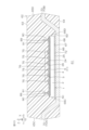
- FIG. 1 is a plan view showing a semiconductor chip according to a first embodiment.
- FIG. 2 is a cross-sectional view taken along the line II-II shown in FIG.
- FIG. 3 is a circuit diagram showing an example of an electrical configuration of the semiconductor chip shown in FIG.
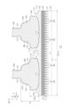
- FIG. 4 is a plan view showing the layout of the output area.
- FIG. 5 is a cross-sectional view taken along line V-V shown in FIG.
- FIG. 6 is a cross-sectional view taken along the line VI-VI shown in FIG.
- FIG. 7 is a cross-sectional view taken along line VII-VII shown in FIG.
- FIG. 8 is a perspective view showing a semiconductor device on which the semiconductor chip shown in FIG. 1 is mounted.
- FIG. 1 is a plan view showing a semiconductor chip according to a first embodiment.
- FIG. 2 is a cross-sectional view taken along the line II-II shown in FIG.
- FIG. 3 is a circuit diagram showing an example of an electrical configuration of the semiconductor
- FIG. 9 is a plan view showing the internal structure of the semiconductor device shown in FIG.
- FIG. 10 is a cross-sectional view taken along line X-X shown in FIG.
- FIG. 11 is a cross-sectional view taken along the line XI-XI shown in FIG.
- FIG. 12 is an enlarged plan view of a portion of FIG. 13 is a cross-sectional view taken along line XIII-XIII shown in FIG. 12.
- FIG. 14 is a cross-sectional view taken along the line XIV-XIV shown in FIG. 12.
- FIG. 15A is an enlarged view of a portion surrounded by a two-dot chain line XV in FIG.
- FIG. 15B is a cross-sectional view of the pseudo bump taken along the second direction.
- FIG. 15A is an enlarged view of a portion surrounded by a two-dot chain line XV in FIG.
- FIG. 15B is a cross-sectional view of the pseudo bump taken along the second direction.
- FIG. 16 is a diagram showing a method of bonding the pseudo bumps to the terminals.
- FIG. 17 is an enlarged plan view of the pseudo bump.
- FIG. 18 is a plan view showing a first layout of pseudo bumps.
- FIG. 19 is a plan view showing a second layout of pseudo bumps.
- FIG. 20 is a plan view showing a modification of the layout of FIG.
- FIG. 21 is a plan view showing a semiconductor chip according to the second embodiment.
- this term includes a numerical value (shape) equal to the numerical value (shape) of the comparison target, as well as a numerical error (shape error) within a range of ⁇ 10% based on the numerical value (shape) of the comparison target.
- terms such as “first,” “second,” and “third” are used, but these are symbols added to the names of each structure to clarify the order of explanation, and are not added with the intention of limiting the names of each structure.
- FIG. 1 is a plan view showing a semiconductor chip 1.
- FIG. 2 is a cross-sectional view taken along line II-II shown in FIG. 1.
- FIG. 3 is a circuit diagram showing an example of the electrical configuration of the semiconductor chip 1 shown in FIG. 1.
- FIG. 3 shows an example in which an inductive load L is connected to the output end (source terminal 26).
- the semiconductor chip 1 includes a substrate 2 formed in a rectangular parallelepiped shape.
- the substrate 2 is made of a Si single crystal substrate.
- the substrate 2 may also be made of a single crystal substrate of a wide band gap semiconductor (e.g., a SiC single crystal substrate).
- the substrate 2 has a first main surface 3 on one side, a second main surface 4 on the other side, and first to fourth side surfaces 5A to 5D connecting the first main surface 3 and the second main surface 4.
- the first principal surface 3 and the second principal surface 4 are formed in a quadrangular shape in a plan view (hereinafter simply referred to as "plan view") seen from their normal direction Z.
- the first principal surface 3 is a device surface on which functional devices are formed.
- the second principal surface 4 is a non-device surface.
- the first side surface 5A and the second side surface 5B extend in a first direction X along the first principal surface 3 and face a second direction Y that intersects (specifically, perpendicular to) the first direction X.
- the third side surface 5C and the fourth side surface 5D extend in the second direction Y and face the first direction X.
- the first to fourth side surfaces 5A to 5D may each have a length of 0.1 mm or more and 10 mm or less in plan view.
- the length of the first to fourth side surfaces 5A to 5D may be 0.1 mm or more and 0.5 mm or less, 0.5 mm or more and 1 mm or less, 1 mm or more and 2.5 mm or less, 2.5 mm or more and 5 mm or less, 5 mm or more and 7.5 mm or less, or 7.5 mm or more and 10 mm or less.
- the semiconductor chip 1 includes an output region 6, a current detection region 7, a control region 8, a first temperature measurement region 9, and a second temperature measurement region 10 provided on the first main surface 3.
- the output region 6, the current detection region 7, the control region 8, the first temperature measurement region 9, and the second temperature measurement region 10 may be referred to as the "first device region,” the “second device region,” the “third device region,” the “fourth device region,” and the “fifth device region,” respectively.
- the output area 6 is an area having a functional device configured to generate an output signal that is output to the outside (outside the semiconductor chip 1).
- the output area 6 is partitioned into an L-shape in plan view.
- the output area 6 has a first area 6A that extends in a strip along the first direction X in the area on the first side surface 5A side, and a second area 6B that extends in a strip along the second direction Y in the area on the third side surface 5C side.
- the output area 6 is partitioned in the area on the first side surface 5A side on the first main surface 3.
- the output area 6 may be partitioned into a quadrangle in plan view, or into a polygonal shape other than a quadrangle.
- the position, size, and planar shape of the output area 6 are arbitrary and are not limited to a specific shape.
- the current detection region 7 is a region having a functional device configured to generate a monitor signal for monitoring the output signal.
- the current detection region 7 is preferably adjacent to the output region 6.
- the current detection region 7 has a planar area less than the planar area of the output region 6 and is provided on the inner side of the output region 6.
- the current detection region 7 is arranged so as to be surrounded by the output region 6.
- the term "surrounded” here includes a form in which the current detection region 7 is surrounded by the output region 6 all around, as well as a form in which the current detection region 7 is adjacent to the output region 6 in at least two directions.
- the functional device of the current detection region 7 is formed by utilizing a part of the functional device of the output region 6.
- the control area 8 is an area having multiple types of functional devices configured to generate control signals that control the functional devices in the output area 6.
- the control area 8 is partitioned into an area on the second side 5B side of the output area 6, and faces the output area 6 in the second direction Y.
- the control area 8 may be partitioned into a quadrangle in a plan view, or into a polygonal shape other than a quadrangle.
- the position, size, and planar shape of the control area 8 are arbitrary and are not limited to a specific shape.
- control area 8 has a planar area equal to or less than the planar area of the output area 6.
- the area ratio of the planar area of the control area 8 to the planar area of the output area 6 may be 0.1 or more and 2 or less.
- the area ratio of the planar area of the control area 8 to the planar area of the output area 6 may be 0.1 or more and 0.25 or less, 0.25 or more and 0.5 or less, 0.5 or more and 0.75 or less, 0.75 or more and 1 or less, 1 or more and 1.25 or less, 1.25 or more and 1.5 or less, 1.5 or more and 1.75 or less, or 1.75 or more and 2 or less. It is preferable that the area ratio is less than 1.
- the first temperature measurement area 9 is an area having a functional device configured to generate a temperature measurement signal that monitors the temperature of the output area 6.
- the first temperature measurement area 9 is preferably adjacent to the output area 6.
- the first temperature measurement area 9 has a planar area less than the planar area of the output area 6, and is provided on the inner side of the output area 6.
- the first temperature measurement area 9 is surrounded by the output area 6.
- "Surrounded” here includes a configuration in which the first temperature measurement area 9 is surrounded by the output area 6 all around, as well as a configuration in which the first temperature measurement area 9 is adjacent to the output area 6 in at least two directions.
- the second temperature measurement area 10 is an area having a functional device configured to generate a temperature measurement signal that monitors the temperature of the control area 8.
- the second temperature measurement area 10 is preferably adjacent to the control area 8.
- the second temperature measurement area 10 has a plan area less than the plan area of the control area 8 and is provided on the inner side of the control area 8.
- the second temperature measurement area 10 is surrounded by the control area 8.
- "Surrounded” here includes a configuration in which the second temperature measurement area 10 is surrounded by the control area 8 all around, as well as a configuration in which the second temperature measurement area 10 is adjacent to the control area 8 in at least two directions.
- the semiconductor chip 1 includes n-system insulated gate type main transistors 11 formed in the output region 6. "n" is 2 or more (n ⁇ 2). In FIG. 3, two systems of main transistors 11 are illustrated.
- the main transistors 11 may be referred to as "gate split transistors.”
- the main transistors 11 include n-number of first gates FG, one first drain FD, and one first source FS.
- the main transistor 11 is configured so that n gate signals (gate voltages), which may be the same or different, are input to n first gates FG at any timing.
- Each gate signal includes an on signal that controls part of the main transistor 11 to the on state, and an off signal that controls part of the main transistor 11 to the off state.
- the main transistor 11 generates a single output current IO (output signal) in response to n gate signals.
- the main transistor 11 is a multi-input single-output switching device.
- the output current IO is a drain-source current that flows between the first drain FD and the first source FS.
- the output current IO is output outside the substrate 2.
- the main transistor 11 includes n system transistors 12.
- n system transistors 12 In FIG. 3, a first system transistor 12A and a second system transistor 12B are illustrated.
- the n system transistors 12 are formed together in a single output region 6, and are configured to be controlled to be electrically independent of one another and turned on and off.
- the n system transistors 12 are connected in parallel to each other so that n gate signals are input separately.
- the n system main transistors 11 are configured so that the system transistors 12 in the on state and the system transistors 12 in the off state coexist at any timing.
- the n system transistors 12 each include a second gate SG, a second drain SD, and a second source SS.
- the n second gates SG each constitute n first gates FG.
- the n second drains SD each constitute one first drain FD.
- the n second sources SS each constitute one first source FS.
- the n system transistors 12 each generate a system current IS in response to a corresponding gate signal.
- the system current IS is a drain-source current flowing between the second drain SD and the second source SS of the system transistor 12.
- the n system currents IS may be different from each other or may be equal to each other.
- the n system currents IS are added between the first drain FD and the first source FS. This generates a single output current IO consisting of the sum of the n system currents IS.
- the semiconductor chip 1 includes m-system insulated gate type monitor transistors 13 formed in the current detection region 7. "m" is 1 or more (m ⁇ 1). In Figure 3, two systems of monitor transistors 13 are illustrated.
- the monitor transistors 13 are connected in parallel to the main transistor 11 and are configured to monitor a part or all of the output current IO. In other words, the monitor transistor 13 is connected in parallel to at least one system transistor 12 and monitors at least one system current IS.
- the monitor transistor 13 is preferably connected in parallel to a plurality of system transistors 12 and configured to monitor a plurality of system currents IS.
- n systems will be replaced with “n systems” and “m pieces” with “n pieces” as necessary.
- the monitor transistor 13 includes n first monitor gates FMG, one first monitor drain FMD, and one first monitor source FMS.
- the n first monitor gates FMG are each configured to receive n monitor gate signals (monitor gate voltages) individually.
- the first monitor drain FMD is electrically connected to the first drain FD.
- the first monitor source FMS is electrically isolated from the first source FS.
- the n first monitor gates FMG are input with n monitor gate signals, which may be the same or different, at any timing.
- Each monitor gate signal includes an on signal that controls a portion of the monitor transistors 13 to an on state, and an off signal that controls a portion of the monitor transistors 13 to an off state.
- the monitor transistor 13 generates a single monitor current IM (monitor signal) that monitors n system currents IS (output currents IO) in response to n monitor gate signals.
- the monitor transistor 13 is a multi-input single-output switching device.
- the monitor current IM is a drain-source current that flows between the first monitor drain FMD and the first monitor source FMS.
- the n first monitor gates FMG are electrically connected to the n first gates FG corresponding to them in a one-to-one relationship. Therefore, the n first monitor gates FMG are configured so that monitor gate signals consisting of gate signals are individually input to each of them.
- the monitor transistor 13 is controlled to be turned on and off at the same timing as the main transistor 11, and generates a monitor current IM that increases and decreases in conjunction with the increase and decrease of the output current IO.
- the monitor current IM is output outside the output region 6 via a current path that is electrically independent from the current path of the output current IO.
- the monitor current IM is equal to or less than the output current IO (IM ⁇ IO). It is preferable that the monitor current IM is less than the output current IO (IM ⁇ IO).
- the current ratio IM/IO of the monitor current IM to the output current IO is arbitrary.
- the current ratio IM/IO may be 1/10,000 or more and 1 or less (preferably less than 1).
- the monitor transistor 13 includes m (n in this embodiment) system monitor transistors 14.
- m n in this embodiment
- a first system monitor transistor 14A and a second system monitor transistor 14B are illustrated.
- the number of systems of the monitor transistor 13 is adjusted by the number of system monitor transistors 14.
- n system monitor transistors 14 are electrically connected to n system transistors 12.
- the n system monitor transistors 14 are configured to be controlled to be in an on state or an off state electrically independent of one another. Specifically, the n system monitor transistors 14 are connected in parallel to one another so that n monitor gate signals are input separately. In other words, the monitor transistor 13 is configured so that the system monitor transistor 14 in the on state and the system monitor transistor 14 in the off state coexist at any timing.
- the n system monitor transistors 14 each include a second monitor gate SMG, a second monitor drain SMD, and a second monitor source SMS.
- the n second monitor gates SMG each constitute n first monitor gates FMG.
- the n second monitor drains SMD each constitute one first monitor drain FMD.
- the n second monitor sources SMS each constitute one first monitor source FMS.
- n second monitor gates SMG are input with n monitor gate signals, which may be the same or different, at any timing.
- n monitor gate signals which may be the same or different, at any timing.
- ISM system monitor signal
- the system monitor current ISM is a drain-source current flowing between the second monitor drain SMD and the second monitor source SMS of the system monitor transistor 14.
- the n system monitor currents ISM are added between the first monitor drain FMD and the first monitor source FMS. This generates a single monitor current IM consisting of the sum of the n system monitor currents ISM.
- the n system monitor transistors 14 are electrically connected to the corresponding system transistors 12 in a one-to-one correspondence and are controlled in conjunction with the corresponding system transistors 12. Specifically, the n system monitor transistors 14 are each connected in parallel to the corresponding system transistors 12 so that the system monitor current ISM is output to a current path that is electrically independent from the current path of the system current IS.
- the n second monitor gates SMG are each electrically connected to a corresponding first gate FG in a one-to-one correspondence. That is, in this configuration, a monitor gate signal consisting of a gate signal is input to each of the n second monitor gates SMG.
- the second monitor drain SMD is electrically connected to the first drain FD.
- the second monitor source SMS is electrically isolated from the first source FS.
- the n system monitor transistors 14 are controlled to be turned on and off at the same timing as the corresponding system transistors 12, and each generates a system monitor current ISM that increases and decreases in conjunction with the increase and decrease of the corresponding system current IS.
- the system monitor current ISM is electrically independent from the system current IS and is taken out from the second monitor source SMS.
- Each system monitor current ISM is equal to or less than the corresponding system current IS (ISM ⁇ IS). It is preferable that each system monitor current ISM is less than the corresponding system current IS (ISM ⁇ IS).
- the current ratio ISM/IS of the system monitor current ISM to the system current IS is arbitrary.
- the current ratio ISM/IS may be 1/10,000 or more and 1 or less (preferably less than 1).
- a gate signal i.e., an on signal
- the first system transistor 12A and the second system transistor 12B are turned on.
- the channel utilization rate of the main transistor 11 increases relatively, and the on resistance decreases relatively. This control is applied during normal operation of the main transistor 11.
- the first system monitor transistor 14A and the second system monitor transistor 14B are turned on in conjunction with the main transistor 11.
- the monitor transistor 13 generates a monitor current IM including the system monitor current ISM of the first system monitor transistor 14A and the system monitor current ISM of the second system monitor transistor 14B.
- the channel utilization rate of the monitor transistor 13 increases relatively, and the on-resistance decreases relatively.
- a gate signal equal to or greater than the gate threshold voltage i.e., an ON signal
- a gate signal equal to or less than the gate threshold voltage i.e., an OFF signal
- the main transistor 11 generates an output current IO that includes the system current IS of the first system transistor 12A.
- the channel utilization rate of the main transistor 11 decreases relatively, and the on-resistance increases relatively. This control is applied during active clamp operation of the main transistor 11.
- the first system monitor transistor 14A is turned on in conjunction with the main transistor 11, and the second system monitor transistor 14B is turned off.
- the monitor transistor 13 generates a monitor current IM that includes the system monitor current ISM of the first system monitor transistor 14A.
- the channel utilization rate of the monitor transistor 13 decreases relatively, and the on-resistance increases relatively.
- the semiconductor chip 1 includes a first temperature sensing diode 15 as an example of a first temperature sensor formed in the first temperature sensing region 9.
- the first temperature sensing diode 15 has a temperature characteristic with respect to the forward voltage that varies according to the temperature T1 of the output region 6, and generates a first temperature sensing signal ST1 that detects the temperature of the output region 6.
- the forward voltage may have a negative temperature characteristic that decreases linearly as the temperature of the output region 6 increases.
- the semiconductor chip 1 includes a second temperature sensing diode 16 as an example of a second temperature sensor formed in the second temperature sensing region 10.
- the second temperature sensing diode 16 has a temperature characteristic with respect to the forward voltage that varies according to the temperature T2 of the control region 8, and generates a second temperature sensing signal ST2 that detects the temperature of the control region 8.
- the forward voltage may have a negative temperature characteristic that decreases linearly as the temperature of the control region 8 increases.
- the second temperature sensing diode 16 preferably has substantially the same configuration as the first temperature sensing diode 15, and preferably has substantially the same electrical characteristics as the first temperature sensing diode 15.
- the temperature T2 of the control region 8 is less than the temperature T1 of the output region 6 (T2 ⁇ T1). Therefore, when the output current IO is being generated, the forward voltage of the second temperature sensing diode 16 is greater than the forward voltage of the first temperature sensing diode 15.
- the semiconductor chip 1 includes a control circuit 17 formed in the control region 8.
- the control circuit 17 may be referred to as a "control IC (Control Integrated Circuit).”
- the IPD may be referred to as an IPM (Intelligent Power Module).
- the control circuit 17 includes multiple types of functional circuits that realize various functions in response to electrical signals input from the outside.
- control circuit 17 includes a gate drive circuit 18, an active clamp circuit 19, an overcurrent protection circuit 20, and an overheat protection circuit 21.
- the overcurrent protection circuit 20 may be referred to as an "OCP (Over Current Protection) circuit”
- the overheat protection circuit 21 may be referred to as a "TSD (Thermal Shutdown) circuit”.
- OCP Over Current Protection
- TSD Thermal Shutdown
- the gate drive circuit 18 is electrically connected to the first gate FG of the main transistor 11 and the first monitor gate FMG of the monitor transistor 13, and generates a gate signal that controls the main transistor 11 and the monitor transistor 13 in response to an external electrical signal.
- the active clamp circuit 19 is electrically connected to the main transistor 11 and the gate drive circuit 18. Specifically, the active clamp circuit 19 is electrically connected to a part (not all) of the first gate FG, the first drain FD, and the gate drive circuit 18.
- the active clamp circuit 19 may include a first diode stage 19a, a second diode stage 19b, and an n-channel MISFET 19c.
- the first diode stage 19a includes one or more Zener diodes forming a forward series circuit.
- the cathode of the first diode stage 19a is electrically connected to the first drain FD.
- the second diode stage 19b includes one or more pn junction diodes forming a forward series circuit.
- the anode of the second diode stage 19b is reverse-bias connected to the anode of the first diode stage 19a.
- the cathode of the second diode stage 19b is electrically connected to the gate drive circuit 18.
- the gate of MISFET 19c is electrically connected to the cathode of the second diode stage 19b.
- the backgate of MISFET 19c is electrically connected to the first source FS.
- the drain of MISFET 19c is connected to the first drain FD.
- the source of MISFET 19c is electrically connected to a part (but not all) of the first gate FG.
- the active clamp circuit 19 cooperates with the gate drive circuit 18 to limit (clamp) the output voltage when a back electromotive force is input to the main transistor 11 due to the energy stored in the inductive load L, thereby protecting the main transistor 11 from the back electromotive force.
- the active clamp circuit 19 is configured to limit the output voltage until the back electromotive force is consumed by performing an active clamp operation on the main transistor 11 when the back electromotive force is input.
- the active clamp circuit 19 cooperates with the gate drive circuit 18 to control a portion of the main transistors 11 (e.g., the first system transistors 12A) to an on state and a portion of the main transistors 11 (e.g., the second system transistors 12B) to an off state.
- the active clamp circuit 19 cooperates with the gate drive circuit 18 to control a portion of the monitor transistors 13 (e.g., the first system monitor transistor 14A) to an on state and a portion of the monitor transistors 13 (e.g., the second system monitor transistor 14B) to an off state.
- the active clamp circuit 19 may be configured to control the on/off of n system transistors 12 (system monitor transistors 14) when the first source FS of the main transistor 11 becomes equal to or lower than a predetermined voltage (e.g., a predetermined negative voltage).
- a predetermined voltage e.g., a predetermined negative voltage
- the overcurrent protection circuit 20 is electrically connected to the monitor transistor 13 and the gate drive circuit 18.
- the overcurrent protection circuit 20 is electrically connected to the first monitor source FMS of the monitor transistor 13, and is configured to receive a part or all (all in this embodiment) of the monitor current IM.
- the overcurrent protection circuit 20 cooperates with the gate drive circuit 18 to control the gate signal and protect the main transistor 11 from overcurrent.
- the overcurrent protection circuit 20 may be configured to generate an overcurrent detection signal SC when the monitor current IM exceeds a predetermined threshold, and output the overcurrent detection signal SC to the gate drive circuit 18.
- the overcurrent detection signal SC is a signal for limiting some or all of the n gate signals generated in the gate drive circuit 18 to a predetermined value or less (e.g., OFF).
- the gate drive circuit 18 limits some or all of the n gate signals in response to the overcurrent detection signal SC, suppressing the overcurrent flowing through the main transistor 11.
- the overcurrent protection circuit 20 switches the gate drive circuit 18 (main transistor 11) to normal control.
- the overheat protection circuit 21 is electrically connected to the first temperature sensing diode 15, the second temperature sensing diode 16, and the gate drive circuit 18.
- the overheat protection circuit 21 is configured to cooperate with the gate drive circuit 18 to control the gate signal and protect the main transistor 11 from overheating.
- the overheat protection circuit 21 receives a first temperature detection signal ST1 from the first temperature sensing diode 15 and a second temperature detection signal ST2 from the second temperature sensing diode 16.
- the overheat protection circuit 21 may be configured to generate an overheat detection signal SH when the difference between the first temperature detection signal ST1 and the second temperature detection signal ST2 exceeds a predetermined threshold, and to output the overheat detection signal SH to the gate drive circuit 18.
- the overheat detection signal SH is a signal for restricting some or all of the n gate signals generated in the gate drive circuit 18 to off.
- the gate drive circuit 18 controls some or all of the main transistors 11 to the off state in response to the overheat detection signal SH, suppressing a temperature rise in the output area 6.
- the gate drive circuit 18 also controls some or all of the monitor transistors 13 to the off state in response to the overheat detection signal SH, suppressing a temperature rise in the current detection area 7 (output area 6).
- the overheat protection circuit 21 transitions the gate drive circuit 18 to normal control.
- the semiconductor chip 1 includes an interlayer insulating film 24 that covers the first main surface 3.
- the interlayer insulating film 24 collectively covers the output region 6, the current detection region 7, the control region 8, the first temperature measurement region 9, and the second temperature measurement region 10.
- the interlayer insulating film 24 has a multilayer wiring structure that includes multiple insulating films stacked on the first main surface 3, and multiple wirings arranged on any of the insulating films.
- Each insulating film may include at least one of a silicon oxide film and a silicon nitride film.
- Each wiring may include at least one of a pure Al layer (an Al layer having a purity of 99% or more), a Cu layer (a Cu layer having a purity of 99% or more), an AlCu alloy layer, an AlSiCu alloy layer, and an AlSi alloy layer.
- the semiconductor chip 1 includes a plurality of terminals 25-30.
- the number and layout of the plurality of terminals 25-30 are appropriately adjusted according to the specifications of the main transistor 11 and the specifications of the control circuit 17.
- the plurality of terminals 25-30 include a drain terminal 25 (power supply terminal), a source terminal 26 (output terminal), a first control terminal 27, a second control terminal 28, a third control terminal 29, and a fourth control terminal 30.
- the drain terminal 25 covers the second main surface 4 of the substrate 2 and is electrically connected to the second main surface 4.
- the drain terminal 25 may include at least one of a Ti layer, a Ni layer, an Au layer, an Ag layer, and an Al layer.
- the drain terminal 25 may have a layered structure in which at least two of a Ti layer, a Ni layer, an Au layer, an Ag layer, and an Al layer are layered in any manner.
- the drain terminal 25 is electrically connected to the first drain FD of the main transistor 11 and transmits the power supply potential.
- the source terminal 26 is disposed on the interlayer insulating film 24.
- the source terminal 26 covers the output region 6 so as to expose the control region 8 in a planar view.
- the layout of the source terminal 26 is adjusted according to the layout of the output region 6 and is not limited to a specific form.
- the source terminal 26 is formed in a quadrangular shape (specifically, a rectangular shape extending in the first direction X) in a planar view.
- the source terminal 26 may be formed in a polygonal shape other than a quadrangular shape in a planar view.
- the source terminal 26 has a rectangular cutout portion 26a that exposes the first temperature detection region 9 (first temperature sensing diode 15).
- the source terminal 26 is electrically connected to the first source FS of the main transistor 11 and transmits the output current IO to the outside.
- the source terminal 26 may include either or both of an Al-based metal layer and a Cu-based metal layer.
- the source terminal 26 may include at least one of a pure Al layer, a pure Cu layer, an AlCu alloy layer, an AlSiCu alloy layer, and an AlSi alloy layer.
- the first to fourth control terminals 27 to 30 are disposed on the interlayer insulating film 24.
- the first to fourth control terminals 27 to 30 may be, for example, an input terminal that provides an input signal to the control circuit 17, an enable terminal that provides an enable signal to the control circuit 17, a self-diagnosis output terminal that outputs an electrical signal for diagnosing the state of the control circuit 17, and a ground terminal that provides a ground potential to the control circuit 17.
- the first to fourth control terminals 27 to 30 each cover an area outside the output area 6 (specifically, the control area 8) in a plan view.
- the first to fourth control terminals 27 to 30 each have a planar area less than the planar area of the source terminal 26.
- the first to fourth control terminals 27 to 30 may include at least one of a pure Al layer, a pure Cu layer, an AlCu alloy layer, an AlSiCu alloy layer, and an AlSi alloy layer.
- Fig. 4 is a plan view showing the layout of the output area 6.
- Fig. 5 is a cross-sectional view taken along line V-V shown in Fig. 4.
- Fig. 6 is a cross-sectional view taken along line VI-VI shown in Fig. 4.
- Fig. 7 is a cross-sectional view taken along line VII-VII shown in Fig. 4.
- the semiconductor chip 1 includes a first semiconductor region 31 of n-type (first conductivity type) formed in a surface layer portion of the first main surface 3 of the substrate 2.
- the first semiconductor region 31 forms the first drain FD of the main transistor 11 and the first monitor drain FMD of the monitor transistor 13.
- the first semiconductor region 31 may be referred to as a "drift region.”
- the first semiconductor region 31 is formed over the entire surface layer of the first main surface 3, and is exposed from the first main surface 3 and the first to fourth side surfaces 5A to 5D.
- the thickness of the first semiconductor region 31 may be 5 ⁇ m or more and 30 ⁇ m or less.
- the thickness of the first semiconductor region 31 is preferably 10 ⁇ m or more and 20 ⁇ m or less.
- the first semiconductor region 31 is formed by an n-type epitaxial layer (Si epitaxial layer).
- the semiconductor chip 1 includes an n-type second semiconductor region 32 formed in a surface layer portion of the second main surface 4 of the substrate 2.
- the second semiconductor region 32 together with the first semiconductor region 31, forms the first drain FD of the main transistor 11 and the first monitor drain FMD of the monitor transistor 13.
- the second semiconductor region 32 may be referred to as a "drain region.”
- the second semiconductor region 32 is formed over the entire surface layer of the second main surface 4 so as to be electrically connected to the first semiconductor region 31, and is exposed from the second main surface 4 and the first to fourth side surfaces 5A to 5D.
- the second semiconductor region 32 is thicker than the first semiconductor region 31.
- the thickness of the second semiconductor region 32 may be 10 ⁇ m or more and 450 ⁇ m or less.
- the thickness of the second semiconductor region 32 is preferably 50 ⁇ m or more and 150 ⁇ m or less.
- the second semiconductor region 32 is formed from an n-type semiconductor substrate (Si semiconductor substrate).
- the semiconductor chip 1 includes a p-type (second conductivity type) body region 33 formed in the surface layer of the first semiconductor region 31 in the output region 6 and the current detection region 7.
- the body region 33 is formed at a distance from the bottom of the first semiconductor region 31 toward the first main surface 3, and faces the second semiconductor region 32 across a portion of the first semiconductor region 31.
- the semiconductor chip 1 includes a plurality of trench structures 35 formed on the first main surface 3 in the output region 6.
- the trench structures 35 may be referred to as "trench gate structures.”
- the plurality of trench structures 35 includes a plurality of trench structures 35 for the main transistors 11 formed in the output region 6, and a plurality of trench structures 35 for the monitor transistors 13 formed in the current detection region 7.
- the number of the plurality of trench structures 35 for the monitor transistors 13 is less than the number of the plurality of trench structures 35 for the main transistors 11.
- the multiple trench structures 35 are arranged at intervals in the first direction X in a plan view, and are each formed in a strip extending in the second direction Y.
- the multiple trench structures 35 penetrate the body region 33 to reach the first semiconductor region 31.
- the multiple trench structures 35 are formed at intervals from the bottom of the first semiconductor region 31 toward the first main surface 3, and face the second semiconductor region 32 across a portion of the first semiconductor region 31.
- Each trench structure 35 has a first width W1 and a first depth D1.
- the first width W1 is the width in a direction perpendicular to the direction in which the trench structure 35 extends.
- the first width W1 may be 0.5 ⁇ m or more and 2 ⁇ m or less.
- the first width W1 is preferably 0.5 ⁇ m or more and 1.5 ⁇ m or less.
- the first depth D1 may be 1 ⁇ m or more and 10 ⁇ m or less.
- the first depth D1 is preferably 2 ⁇ m or more and 6 ⁇ m or less.
- the bottom wall of each trench structure 35 is preferably spaced 1 ⁇ m or more and 5 ⁇ m or less from the bottom of the first semiconductor region 31.
- the multiple trench structures 35 are arranged in the first direction X with a trench spacing IT between them.
- the trench spacing IT may be 0.25 to 1.5 times the first width W1. It is preferable that the trench spacing IT is equal to or smaller than the first width W1.
- the trench spacing IT may be 0.5 ⁇ m to 2 ⁇ m.
- the trench structure 35 has a multi-electrode structure including a trench 36, a first insulating film 37, a second insulating film 38, a first electrode 39, a second electrode 40, and a third insulating film 41.
- the trench structure 35 includes an electrode (gate electrode) embedded in the trench 36 with an insulator (gate insulator) sandwiched between them.
- the insulator is composed of the first insulating film 37, the second insulating film 38, and the third insulating film 41.
- the electrode is composed of the first electrode 39 and the second electrode 40.
- the trench 36 is dug down from the first main surface 3 toward the second main surface 4, and defines the wall surface of the trench structure 35.
- the first insulating film 37 covers the upper wall surface of the trench 36 in a film-like manner. Specifically, the first insulating film 37 covers the upper wall surface located in the region on the opening side of the trench 36 relative to the bottom of the body region 33.
- the first insulating film 37 crosses the boundary between the first semiconductor region 31 and the body region 33, and has a portion covering the first semiconductor region 31.
- the first insulating film 37 may include a silicon oxide film.
- the first insulating film 37 preferably includes a silicon oxide film made of an oxide of the substrate 2.
- the first insulating film 37 is formed as a gate insulating film.
- the second insulating film 38 covers the lower wall surface of the trench 36 in a film-like shape. Specifically, the second insulating film 38 covers the lower wall surface located in the region on the bottom wall side of the trench 36 relative to the bottom of the body region 33.
- the second insulating film 38 covers the first semiconductor region 31.
- the second insulating film 38 may include a silicon oxide film. It is preferable that the second insulating film 38 includes a silicon oxide film made of an oxide of the substrate 2. It is preferable that the second insulating film 38 is thicker than the first insulating film 37.
- the first electrode 39 is embedded in the upper side (opening side) of the trench 36 with the first insulating film 37 in between.
- the first electrode 39 is embedded in a strip shape extending in the second direction Y in a plan view.
- the first electrode 39 faces the body region 33 and the first semiconductor region 31 with the first insulating film 37 in between.
- the first electrode 39 may include conductive polysilicon.
- the first electrode 39 is formed as a gate electrode. A gate signal is input to the first electrode 39.
- the second electrode 40 is embedded in the lower side (bottom wall side) of the trench 36 with the second insulating film 38 in between.
- the second electrode 40 is embedded in a strip shape extending in the second direction Y in a plan view.
- the second electrode 40 may have a thickness (length) in the depth direction of the trench 36 that exceeds the thickness (length) of the first electrode 39.
- the second electrode 40 faces the first semiconductor region 31 with the second insulating film 38 in between.
- the second electrode 40 has an upper end that protrudes from the second insulating film 38 toward the first main surface 3.
- the upper end of the second electrode 40 engages with the bottom of the second electrode 40 and faces the first insulating film 37 with the bottom of the second electrode 40 in between in the horizontal direction along the first main surface 3.
- the second electrode 40 may include conductive polysilicon.
- the second electrode 40 is formed as a gate electrode and is fixed at the same potential as the first electrode 39. That is, the same gate signal is applied to the second electrode 40 at the same time as the first electrode 39. This suppresses the voltage drop between the first electrode 39 and the second electrode 40, and as a result, electric field concentration between the first electrode 39 and the second electrode 40 is suppressed.
- the carrier density in the vicinity of the trench 36 increases, and as a result, the on-resistance of the substrate 2 (particularly the first semiconductor region 31) decreases.
- the third insulating film 41 is interposed between the first electrode 39 and the second electrode 40, and electrically insulates the first electrode 39 and the second electrode 40.
- the third insulating film 41 covers the portion of the second electrode 40 exposed from the second insulating film 38, and is continuous with the first insulating film 37 and the second insulating film 38.
- the third insulating film 41 may include a silicon oxide film. It is preferable that the third insulating film 41 includes a silicon oxide film made of an oxide of the second electrode 40. It is preferable that the third insulating film 41 is thinner than the second insulating film 38.
- the semiconductor chip 1 includes a plurality of trench connection structures 45 formed on the first main surface 3 in the output region 6.
- the plurality of trench connection structures 45 are formed in a region on one end side of the plurality of trench structures 35 and a region on the other end side of the plurality of trench structures 35, respectively. In FIG. 4, the region on one end side of the plurality of trench structures 35 is shown.
- the multiple trench connection structures 45 are each formed in a band extending in the second direction Y so as to connect one end of at least two (two in this embodiment) trench structures 35 adjacent in the first direction X.
- the multiple trench connection structures 45 are each formed in a band extending in the second direction Y so as to connect the other end of at least two (two in this embodiment) trench structures 35 adjacent in the first direction X.
- the multiple trench connection structures 45 together with the multiple trench structures 35, each constitute a single annular or ladder-shaped unit trench structure in a plan view.
- the multiple trench connection structures 45 are formed at intervals from the bottom of the first semiconductor region 31 toward the first main surface 3, and face the second semiconductor region 32 across a portion of the first semiconductor region 31.
- the trench connection structure 45 on the other side has a structure similar to that of the trench connection structure 45 on one side, except that it is connected to the other ends of the multiple trench structures 35. Below, the configuration of one trench connection structure 45 on one side is described, and a description of the trench connection structure 45 on the other side is omitted.
- the trench connection structure 45 has a first trench portion 45a extending in a first direction X and multiple (two in this embodiment) second trench portions 45b extending in a second direction Y.
- the first trench portion 45a faces multiple one ends in a plan view.
- the multiple second trench portions 45b extend from the first trench portion 45a toward one ends of the multiple trench structures 35 and are connected to the multiple one ends.
- the trench connection structure 45 has a second width W2 and a second depth D2.
- the second width W2 is the width in a direction perpendicular to the direction in which the trench connection structure 45 extends.
- the second width W2 is preferably approximately equal to the first width W1 of the trench structure 35.
- the second depth D2 is preferably approximately equal to the first depth D1 of the trench structure 35.
- the bottom wall of the trench connection structure 45 is preferably spaced from the bottom of the first semiconductor region 31 by a distance of 1 ⁇ m to 5 ⁇ m.
- the trench connection structure 45 has a single electrode structure including a connection trench 46, a connection insulating film 47, and a connection electrode 48.
- the connection trench 46 is dug down from the first main surface 3 toward the second main surface 4, and defines the wall surface of the trench connection structure 45.
- the sidewalls and bottom wall of the connection trench 46 are connected to the sidewalls and bottom wall of the trench 36 of the trench structure 35.
- connection insulating film 47 covers the wall surface of the connection trench 46 in the form of a film.
- the connection insulating film 47 is connected to the first insulating film 37 and the second insulating film 38 at the communicating portion between the trench 36 and the connection trench 46.
- the connection insulating film 47 may include a silicon oxide film.
- the connection insulating film 47 preferably includes a silicon oxide film made of an oxide of the substrate 2.
- the connection insulating film 47 is preferably thicker than the first insulating film 37. The thickness of the connection insulating film 47 may be approximately equal to the thickness of the second insulating film 38.
- connection electrode 48 is embedded in the connection trench 46 with a connection insulating film 47 in between.
- the connection electrode 48 may include conductive polysilicon.
- the connection electrode 48 extends in the first direction X in the first trench portion 45a and in the second direction Y in the second trench portion 45b.
- the connection electrode 48 is connected to the second electrode 40 at the communicating portion between the trench 36 and the connection trench 46, and faces the first electrode 39 with a third insulating film 41 in between.
- the same gate signal is applied to the connection electrode 48 at the same time as the first electrode 39 and the second electrode 40.
- the semiconductor chip 1 includes a plurality of n-type source regions 51 formed in regions along the plurality of trench structures 35 in the surface layer portion of the body region 33 of the output region 6 and the current detection region 7.
- the n-type impurity concentration of the plurality of source regions 51 is higher than that of the first semiconductor region 31.
- the plurality of source regions 51 are respectively disposed on both sides of each trench structure 35 and are arranged at intervals along each trench structure 35.
- the plurality of source regions 51 are formed at intervals from the bottom of the body region 33 toward the first main surface 3, and face the first electrode 39 with the corresponding first insulating film 37 sandwiched therebetween.
- the multiple source regions 51 along one trench structure 35 are preferably arranged offset in the second direction Y with respect to the multiple source regions 51 along the other trench structure 35.
- the multiple source regions 51 along one trench structure 35 are preferably opposed in the first direction X to the region between the multiple source regions 51 along the other trench structure 35.
- the semiconductor chip 1 includes a plurality of p-type contact regions 52 formed in the surface layer of the body region 33 of the output region 6 and the current detection region 7 along the plurality of trench structures 35.
- the p-type impurity concentration of the plurality of contact regions 52 is higher than that of the body region 33.
- the contact regions 52 are disposed on both sides of each trench structure 35 and are arranged at intervals along each trench structure 35.
- the contact regions 52 are formed at intervals from the bottom of the body region 33 toward the first main surface 3, and face the first electrodes 39 with the corresponding first insulating films 37 interposed therebetween.
- the multiple contact regions 52 are arranged alternately with the multiple source regions 51 on both sides of each trench structure 35. It is preferable that the multiple contact regions 52 along one trench structure 35 are arranged offset in the second direction Y with respect to the multiple contact regions 52 along the other trench structure 35. In other words, it is preferable that the multiple contact regions 52 along one trench structure 35 face the region between the multiple contact regions 52 along the other trench structure 35 (i.e., the source region 51) in the first direction X.
- the semiconductor chip 1 includes n gate wirings 53 arranged in the aforementioned interlayer insulating film 24 in a mutually electrically independent state.
- the n gate wirings 53 include n gate wirings 53 for the main transistor 11 and n gate wirings 53 for the monitor transistor 13.
- the n gate wirings 53 are selectively electrically connected to at least one corresponding trench structure 35 through a plurality of first via electrodes 54 in the output region 6 and the current detection region 7, and are electrically connected to the control circuit 17 (gate drive circuit 18) in the control region 8.
- the plurality of first via electrodes 54 may contain tungsten.
- n gate wirings 53 for the main transistors 11 are electrically connected to at least one (in this embodiment, multiple) trench structures 35 and at least one (in this embodiment, multiple) trench connection structures 45 that are to be systemized (grouped) as system transistors 12 via multiple first via electrodes 54 in the output region 6.
- the n gate wirings 53 for the main transistors 11 include a first gate wiring 53A for the first system transistors 12A and a second gate wiring 53B for the second system transistors 12B.
- the first gate wiring 53A is electrically connected to a plurality of unit trench structures (a plurality of trench structures 35 and a plurality of trench connection structures 45) to be organized (grouped) as the first system transistors 12A through a plurality of first via electrodes 54 in the output region 6.
- the second gate wiring 53B is disposed in the interlayer insulating film 24 in a state electrically independent from the first gate wiring 53A.
- the second gate wiring 53B is electrically connected to a plurality of unit trench structures (a plurality of trench structures 35 and a plurality of trench connection structures 45) to be organized (grouped) as the second system transistor 12B through a plurality of first via electrodes 54 in the output region 6.
- the plurality of unit trench structures for the second system transistor 12B are organized alternately with the plurality of unit trench structures for the first system transistor 12A.
- the n gate wirings 53 for the monitor transistor 13 are electrically connected to at least one (in this embodiment, multiple) trench structures 35 and at least one (in this embodiment, multiple) trench connection structures 45 to be systemized (grouped) as the system monitor transistor 14 through multiple first via electrodes 54 in the current detection region 7.
- the number of trench structures 35 (the number of trench connection structures 45) constituting the system monitor transistor 14 is less than the number of trench structures 35 (the number of trench connection structures 45) constituting the system transistor 12.
- the n gate wirings 53 for the monitor transistors 13 include a first gate wiring 53A for the first system monitor transistor 14A and a second gate wiring 53B for the second system monitor transistor 14B.
- the first gate wiring 53A is electrically connected to at least one trench structure 35 and at least one trench connection structure 45 to be organized as the first system monitor transistor 14A through a plurality of first via electrodes 54 in the current detection region 7.
- the second gate wiring 53B is disposed in the interlayer insulating film 24 in a state electrically independent from the first gate wiring 53A.
- the second gate wiring 53B is electrically connected to at least one trench structure 35 and at least one trench connection structure 45 to be organized as the second system monitor transistor 14B through a plurality of first via electrodes 54 in the current detection region 7.
- the trench structure 35 for the second system monitor transistor 14B may be adjacent to the trench structure 35 for the first system monitor transistor 14A.
- the first gate wiring 53A for the monitor transistor 13 may be formed integrally with the first gate wiring 53A for the main transistor 11. Also, the second gate wiring 53B for the monitor transistor 13 may be formed integrally with the second gate wiring 53B for the main transistor 11.
- the semiconductor chip 1 includes a plurality of source wirings 55 arranged in the interlayer insulating film 24.
- the plurality of source wirings 55 includes a first source wiring 55A for the main transistor 11 and a second source wiring 55B for the monitor transistor 13.
- the first source wiring 55A covers the output region 6 in the interlayer insulating film 24, and is electrically connected to the plurality of source regions 51 and the plurality of contact regions 52 through the plurality of second via electrodes 56.
- the plurality of second via electrodes 56 may contain tungsten.
- the second source wiring 55B is selectively routed in the region between the current detection region 7 and the control region 8 within the interlayer insulating film 24.
- the second source wiring 55B is electrically connected to the multiple source regions 51 and multiple contact regions 52 through multiple second via electrodes 56 in the current detection region 7, and is electrically connected to the control circuit 17 (overcurrent protection circuit 20) in the control region 8.
- the semiconductor chip 1 includes the aforementioned source terminal 26 disposed on the interlayer insulating film 24.
- the source terminal 26 overlaps the multiple source wirings 55 (first source wiring 55A and second source wiring 55B) in a plan view, and covers all of the trench structures 35 and all of the trench connection structures 45.
- the source terminal 26 is electrically connected to the first source wiring 55A through a plurality of third via electrodes 57 arranged in the interlayer insulating film 24.
- the plurality of third via electrodes 57 are arranged in the region between the plurality of second via electrodes 56 in plan view and cross-sectional view. In other words, in this embodiment, the plurality of third via electrodes 57 do not face the second via electrode 56 across the first source wiring 55A. Of course, the plurality of third via electrodes 57 may face the second via electrode 56 across the first source wiring 55A.
- the source terminal 26 preferably has a thickness greater than that of the source wiring 55.
- the thickness of the source terminal 26 is preferably greater than the first depth D1 of the multiple trench structures 35 (the second depth D2 of the trench connection structure 45).
- the thickness of the source terminal 26 is preferably greater than the thickness of the interlayer insulating film 24.
- the thickness of the source terminal 26 may be 1 ⁇ m or more and 25 ⁇ m or less.
- the thickness of the source terminal 26 may be 1 ⁇ m or more and 5 ⁇ m or less, 5 ⁇ m or more and 10 ⁇ m or less, 10 ⁇ m or more and 15 ⁇ m or less, 15 ⁇ m or more and 20 ⁇ m or less, or 20 ⁇ m or more and 25 ⁇ m or less.
- the thickness of the source terminal 26 may be 1 ⁇ m or more and 10 ⁇ m or less.
- the thickness of the source terminal 26 may be 10 ⁇ m or more and 25 ⁇ m or less.
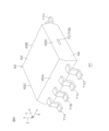
- FIG. 8 is a perspective view showing a semiconductor device 61 on which the semiconductor chip 1 shown in FIG. 1 is mounted.
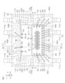
- FIG. 9 is a plan view showing the internal structure of the semiconductor device 61 shown in FIG. 8.
- FIG. 10 is a cross-sectional view taken along line X-X shown in FIG. 9.
- FIG. 11 is a cross-sectional view taken along line XI-XI shown in FIG. 9.
- FIG. 12 is a plan view showing an enlarged portion of FIG. 9.
- FIG. 13 is a cross-sectional view taken along line XIII-XIII shown in FIG. 12.
- FIG. 14 is a cross-sectional view taken along line XIV-XIV shown in FIG. 12.
- semiconductor device 61 may be referred to as a "semiconductor package” or a “semiconductor module.”
- the package type of semiconductor device 61 may take various forms depending on the usage environment, the mounting target, the form of semiconductor chip 1, etc. Here, an example is shown in which semiconductor device 61 is an 8-terminal type SOP (Small Outline Package).
- the semiconductor device 61 includes a package body 62 having a rectangular parallelepiped shape.
- the package body 62 includes a matrix resin and a plurality of fillers.
- the matrix resin may be a thermosetting resin (e.g., epoxy resin).
- the plurality of fillers may be insulating spherical objects (e.g., silica particles).
- the package body 62 has a first surface 63 on one side, a second surface 64 on the other side, and first to fourth side walls 65A to 65D connecting the first surface 63 and the second surface 64.
- the first surface 63 is a mounting surface
- the second surface 64 is a non-mounting surface.
- the first surface 63 and the second surface 64 are formed in a quadrangular shape (in this embodiment, a rectangular shape extending in the first direction X) in a plan view.
- the first side wall 65A and the second side wall 65B extend in the first direction X along the first main surface 3 and face the second direction Y.
- the first side wall 65A and the second side wall 65B form the long sides of the package body 62.
- the third side wall 65C and the fourth side wall 65D extend in the second direction Y and face the first direction X.
- the third side wall 65C and the fourth side wall 65D form the short sides of the package body 62.
- the semiconductor device 61 includes a rectangular parallelepiped metal plate 66 disposed within a package body 62.
- the metal plate 66 may be referred to as a metallic "die pad.”
- the metal plate 66 has a first plate surface 67 on one side, a second plate surface 68 on the other side, and first to fourth plate side walls 69A to 69D connecting the first plate surface 67 and the second plate surface 68.
- the first plate surface 67 and the second plate surface 68 are formed in a quadrangular shape (in this embodiment, a rectangular shape extending in the first direction X) in a plan view.
- the second plate surface 68 is exposed from the second surface 64 of the package body 62.
- the metal plate 66 may be disposed within the package body 62 so that the second plate surface 68 is not exposed from the second surface 64.
- the first plate side wall 69A and the second plate side wall 69B extend in the first direction X along the first main surface 3 and face the second direction Y.
- the first plate side wall 69A and the second plate side wall 69B form the long sides of the metal plate 66.
- the third plate side wall 69C and the fourth plate side wall 69D extend in the second direction Y and face the first direction X.
- the third plate side wall 69C and the fourth plate side wall 69D form the short sides of the metal plate 66.
- the semiconductor device 61 includes at least one (in this embodiment, multiple) extension portion 70 that is extended from the metal plate 66 toward at least one of the first to fourth side walls 65A to 65D within the package body 62.
- the multiple extension portions 70 include a first extension portion 70A and a second extension portion 70B.
- the first extension portion 70A is pulled out in a strip-like shape from the third plate side wall 69C toward the third side wall 65C.
- the first extension portion 70A has a bent portion that is bent toward the first surface 63, and is exposed from the middle of the thickness range of the package body 62 at the third side wall 65C.
- the second extension portion 70B is pulled out in a strip-like shape from the fourth plate side wall 69D toward the fourth side wall 65D.
- the second extension portion 70B has a bent portion that is bent toward the first surface 63, and is exposed from the middle of the thickness range of the package body 62 at the fourth side wall 65D.
- the semiconductor device 61 includes first to eighth lead terminals 71A to 71H made of metal and arranged within the package body 62 at intervals from the metal plate 66 so as to be pulled out from inside the package body 62 to the outside.
- the first to fourth lead terminals 71A to 71D are arranged at intervals in the first direction X on the first side wall 65A side, and each is formed in a strip extending in the second direction Y.
- the fifth to eighth lead terminals 71E to 71H are arranged at intervals in the first direction X on the second side wall 65B side, and each is formed in a strip extending in the second direction Y.
- the first to eighth lead terminals 71A to 71H each have an inner end, a band portion, and an outer end.
- the inner end is disposed midway through the thickness range of the package body 62 so as to be located on the first surface 63 side relative to the height position of the metal plate 66.
- the planar shape of the inner end is arbitrary.
- the band portion is drawn out from the inner end to the outside of the package body 62 and is bent towards the second surface 64 outside the package body 62.
- the band portion extends to a height position that crosses the second surface 64 of the package body 62.
- the outer end extends approximately parallel to the second surface 64 at a height position lower than the second surface 64 of the package body 62.
- the semiconductor device 61 includes a semiconductor chip 1 disposed on a metal plate 66 (first plate surface 67) within a package body 62.
- the semiconductor chip 1 is disposed on the metal plate 66 with the drain terminal 25 facing the metal plate 66 (first plate surface 67).
- the semiconductor device 61 includes a conductive bonding material 72 interposed between the semiconductor chip 1 and the metal plate 66 in the package body 62. Specifically, the conductive bonding material 72 is interposed between the drain terminal 25 and the metal plate 66, and electrically and mechanically connects the drain terminal 25 and the metal plate 66.
- the conductive bonding material 72 may include solder or metal paste. The solder may be lead-free solder.
- the metal paste may include at least one of Au, Ag, and Cu.
- the Ag paste may be made of Ag sintered paste.
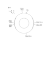
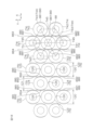
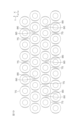
- the semiconductor device 61 includes a plurality of pseudo bumps 75 disposed on the source terminal 26 in a state free from wires within the package body 62.
- Each of the plurality of pseudo bumps 75 is made of a metal mass formed using a wire bonding process for the source terminal 26.
- the wire bonding process is performed using a capillary (wire supply device) of a bonding device.
- the multiple pseudo bumps 75 are arranged on the source terminal 26 more densely than the true bumps 90 described below. "Denser than the true bumps 90" means that the area occupied by the multiple pseudo bumps 75 with respect to the source terminal 26 is larger than that of other structures (the true bumps 90 described below) connected to the source terminal 26.
- the multiple pseudo bumps 75 are arranged on the source terminal 26 with a first occupation area per unit planar area.
- each of the pseudo-bumps 75 has a first size S1 in plan view.
- the first size S1 is defined by the length of the widest portion of the pseudo-bump 75 in plan view.
- the first size S1 may be 50 ⁇ m or more and 250 ⁇ m or less.
- the first size S1 may be 50 ⁇ m or more and 75 ⁇ m or less, 75 ⁇ m or more and 100 ⁇ m or less, 100 ⁇ m or more and 125 ⁇ m or less, 125 ⁇ m or more and 150 ⁇ m or less, 150 ⁇ m or more and 175 ⁇ m or less, 175 ⁇ m or more and 200 ⁇ m or less, 200 ⁇ m or more and 225 ⁇ m or less, or 225 ⁇ m or more and 250 ⁇ m or less. It is preferable that the first size S1 is 75 ⁇ m or more and 200 ⁇ m or less. It is particularly preferable that the first size S1 is 100 ⁇ m or more and 180 ⁇ m or less.
- the multiple pseudo bumps 75 are arranged on the source terminal 26 at a first pitch P1 in a plan view.
- the first pitch P1 is defined by the distance between the centers of the multiple pseudo bumps 75.
- the multiple pseudo bumps 75 may be arranged so as to be in contact with each other at the first pitch P1, or may be arranged at intervals from each other at the first pitch P1. It is preferable that the multiple pseudo bumps 75 are arranged at intervals from each other.
- the first pitch P1 is preferably 1 to 2.5 times the first size S1.
- the ratio P1/S1 of the first pitch P1 to the first size S1 may be 1 to 1.25, 1.25 to 1.5, 1.5 to 1.75, 1.75 to 2, 2 to 2.25, or 2.25 to 2.5. It is preferable that the ratio P1/S1 is greater than 1. It is particularly preferable that the ratio P1/S1 is 1.25 to 1.75.
- the first pitch P1 may be 50 ⁇ m or more and 250 ⁇ m or less.
- the first pitch P1 may be 50 ⁇ m or more and 75 ⁇ m or less, 75 ⁇ m or more and 100 ⁇ m or less, 100 ⁇ m or more and 125 ⁇ m or less, 125 ⁇ m or more and 150 ⁇ m or less, 150 ⁇ m or more and 175 ⁇ m or less, 175 ⁇ m or more and 200 ⁇ m or less, 200 ⁇ m or more and 225 ⁇ m or less, or 225 ⁇ m or more and 250 ⁇ m or less. It is preferable that the first pitch P1 is 75 ⁇ m or more and 200 ⁇ m or less. It is particularly preferable that the first pitch P1 is 100 ⁇ m or more and 180 ⁇ m or less.
- the spacing I between the multiple pseudo bumps 75 may be 0 ⁇ m or more and 100 ⁇ m or less.
- the spacing I may be 0 ⁇ m or more and 10 ⁇ m or less, 10 ⁇ m or more and 20 ⁇ m or less, 20 ⁇ m or more and 30 ⁇ m or less, 30 ⁇ m or more and 40 ⁇ m or less, 40 ⁇ m or more and 50 ⁇ m or less, 50 ⁇ m or more and 60 ⁇ m or less, 60 ⁇ m or more and 70 ⁇ m or less, 70 ⁇ m or more and 80 ⁇ m or less, 80 ⁇ m or more and 90 ⁇ m or less, or 90 ⁇ m or more and 100 ⁇ m or less.
- the spacing I is 10 ⁇ m or more. It is particularly preferable that the spacing I is 30 ⁇ m or more and 60 ⁇ m or less.
- each of the pseudo bumps 75 has a first thickness T1.
- the first thickness T1 is defined by the thickness of the thickest portion of the pseudo bump 75 in a cross-sectional view.
- the first thickness T1 is preferably greater than the first depth D1 of the trench structures 35.
- the first thickness T1 is preferably greater than the thickness of the source terminal 26.
- the first thickness T1 is preferably greater than the thickness of the first semiconductor region 31.
- the first thickness T1 may be greater than the thickness of the substrate 2. Of course, the first thickness T1 may be less than the thickness of the substrate 2.
- the first thickness T1 may be 10 ⁇ m or more and 150 ⁇ m or less.
- the first thickness T1 may be 10 ⁇ m or more and 25 ⁇ m or less, 25 ⁇ m or more and 50 ⁇ m or less, 50 ⁇ m or more and 75 ⁇ m or less, 75 ⁇ m or more and 100 ⁇ m or less, 100 ⁇ m or more and 125 ⁇ m or less, or 125 ⁇ m or more and 150 ⁇ m or less. It is preferable that the first thickness T1 is 25 ⁇ m or more and 100 ⁇ m or less. It is particularly preferable that the first thickness T1 is 50 ⁇ m or more.
- At least three pseudo bumps 75 are arranged on the source terminal 26 as a pseudo bump group 76.
- the at least three pseudo bumps 75 are arranged in a layout in which they are located at the apexes of an isosceles triangle in a planar view. It is particularly preferable that the isosceles triangle is an equilateral triangle.
- multiple pseudo bumps 75 are arranged in a layout in which they are located at the apexes of a triangle in a planar view, and no fourth bump is arranged in the space surrounded by three pseudo bumps 75. This configuration may be defined as "multiple pseudo bumps 75 densely arranged.”
- At least seven pseudo bumps 75 are arranged on the source terminal 26 as a pseudo bump group 76.
- the seven pseudo bumps 75 may include one central bump 73 and six surrounding bumps 74 arranged on concentric circles centered on the center of the central bump 73 in a planar view.
- the six peripheral bumps 74 are arranged in a layout in which they are located at the vertices of a hexagon in a plan view, and the one central bump 73 is arranged in a layout in which they are located at the center of the hexagon in a plan view.
- the multiple pseudo bumps 75 are joined to the source terminal 26 in a layout that results in a hexagonal close-packed array (i.e., a honeycomb array) in a plan view.
- the hexagon is a regular hexagon.
- a pseudo-bump group 76 including 28 pseudo-bumps 75 arranged in a hexagonal close-packed layout is bonded to the source terminal 26.
- the number of pseudo-bumps 75 bonded to the source terminal 26 is arbitrary, but it is preferable that a pseudo-bump group 76 including at least three pseudo-bumps 75 and/or a pseudo-bump group 76 including at least seven pseudo-bumps 75 is bonded to the source terminal 26.
- multiple pseudo-bump groups 76 may be bonded to the source terminal 26 at a distance greater than the first pitch P1 (spacing I).
- the joining points of the multiple pseudo bumps 75 (pseudo bump group 76) to the source terminal 26 may be set based on the temperature distribution of the semiconductor chip 1. For example, the high temperature and low temperature areas of the output area 6 may be analyzed using thermography or a simulation tool, and the multiple pseudo bumps 75 (pseudo bump group 76) may be joined to the portions of the source terminal 26 that cover the high temperature area of the output area 6.
- the multiple pseudo bumps 75 may be joined to the source terminal 26 in a layout in which they are densely packed in the inner part (e.g., the center) of the source terminal 26 and sparsely packed in the peripheral part of the source terminal 26.
- a form in which the multiple pseudo bumps 75 are "sparse" includes a form in which no pseudo bumps 75 are present. In this form, one pseudo bump 75 is disposed on each of the three peripheral parts of the source terminal 26 along each of the three sides.
- the temperature of the control region 8 is lower than the temperature of the output region 6.
- the source terminal 26 covers the output region 6 so as to expose the control region 8, and the multiple pseudo bumps 75 (pseudo bump group 76) are arranged in a region that overlaps the output region 6 in a planar view.
- the multiple pseudo bumps 75 (pseudo bump group 76) are arranged in a position that overlaps the main transistor 11 in a planar view, and are not arranged in a region that overlaps the control region 8 in a planar view.
- pseudo bumps 75 may face the monitor transistor 13 in a plan view. That is, the pseudo bumps 75 (pseudo bump group 76) may face the trench structures 35 for the main transistor 11 and the trench structures 35 for the monitor transistor 13. Of course, the pseudo bumps 75 (pseudo bump group 76) may be disposed on the source terminal 26 so as not to face the trench structures 35 for the monitor transistor 13.
- Each pseudo-bump 75 may face 10 to 200 trench structures 35.
- the number of facing trench structures 35 for each pseudo-bump 75 may be 10 to 25, 25 to 50, 50 to 75, 75 to 100, 100 to 125, 125 to 150, 150 to 175, or 175 to 200.
- the number of facing trench structures 35 for each pseudo-bump 75 is preferably 25 to 100.
- the pseudo bump 75 includes a first bump body 77 and a first bump metal film 78.
- the first bump body 77 includes a first metal.
- the first metal is made of a material different from that of the source terminal 26, and is preferably made of a metal harder than the source terminal 26.
- the first metal includes, for example, at least one of a Cu-based metal, an Al-based metal, an Au-based metal, and an Ag-based metal.
- the Cu-based metal may include pure Cu or a Cu alloy.
- the Al-based metal may include pure Al or an Al alloy.
- the Au-based metal may include pure Au or an Au alloy.
- the Ag-based metal may include pure Ag or an Ag alloy.
- the first bump body 77 includes pure Cu.
- the source terminal 26 is preferably an Al-based metal layer.
- the first bump main body 77 includes a first body portion 79 and a first neck portion 80.
- the first body portion 79 consists of a wide portion connected to the source terminal 26.
- the first body portion 79 is formed in a generally cylindrical shape with outwardly curved side walls in a cross-sectional view.
- the first body portion 79 has a first body size SB1 that forms the first size S1 of the pseudo bump 75 in a plan view.
- the first body portion 79 may have a first body thickness TB1 that is 0.1 to 0.9 times the first thickness T1 of the pseudo bump 75.
- the first body thickness TB1 is preferably greater than the thickness of the first semiconductor region 31.
- the first body thickness TB1 may be greater than the thickness of the substrate 2.
- the first body thickness TB1 may be less than the thickness of the substrate 2.
- the thickness ratio T1/TB1 of the first body thickness TB1 to the first thickness T1 may be 0.1 or more and 0.2 or less, 0.2 or more and 0.3 or less, 0.3 or more and 0.4 or less, 0.4 or more and 0.5 or less, 0.5 or more and 0.6 or less, 0.6 or more and 0.7 or less, 0.7 or more and 0.8 or less, or 0.8 or more and 0.9 or less. It is preferable that the thickness ratio T1/TB1 is 0.4 or more and 0.7 or less. It is particularly preferable that the thickness ratio T1/TB1 is 0.5 or more.
- the first neck portion 80 consists of a portion that protrudes from the first body portion 79 toward the side opposite the source terminal 26 and is narrower than the first body portion 79.
- the first neck portion 80 is formed in a generally cylindrical shape in cross-sectional view.
- the first neck portion 80 has a first upper end portion 81 that slopes diagonally downward.
- the first upper end portion 81 may have an upper end apex portion 82, an upper end base portion 83, and an inclined portion 84 in cross-sectional view.
- the upper end apex 82 is formed on one side of the periphery of the first upper end 81 in a cross-sectional view.
- the upper end base 83 is formed on the other side of the periphery of the first upper end 81 in a cross-sectional view, and is located on the first body part 79 side relative to the height position of the upper end apex 82.
- the inclined portion 84 slopes diagonally downward from the upper end apex 82 to the upper end base 83 in a cross-sectional view.
- the first upper end 81 may have an upper end protrusion 85 that protrudes from the upper end base 83 toward the opposite side to the first body part 79.
- the tip of the upper end protrusion 85 may be formed at a height position on the first body part 79 side relative to the height position of the tip of the upper end apex 82.
- the first neck portion 80 has a first neck size SN1 that is less than the first body size SB1 in a plan view.
- the first neck size SN1 may be 0.1 to 0.9 times the first body size SB1 (first size S1).
- the size ratio SN1/SB1 of the first neck size SN1 to the first body size SB1 may be 0.1 to 0.2, 0.2 to 0.3, 0.3 to 0.4, 0.4 to 0.5, 0.5 to 0.6, 0.6 to 0.7, 0.7 to 0.8, or 0.8 to 0.9. It is preferable that the size ratio SN1/SB1 is 0.5 to 0.7. It is particularly preferable that the size ratio SN1/SB1 is greater than 0.5.
- the first bump metal film 78 contains a second metal different from the first metal of the first bump body 77, and covers at least a portion of the outer surface of the first bump body 77.
- the first bump metal film 78 covers the area outside the upper end apex 82 of the outer surface of the first bump body 77 so as to expose the upper end apex 82.
- the first bump metal film 78 is shown covering the entire area outside the top end 82, but the first bump metal film 78 does not necessarily have to have such a shape.
- the shape of the first bump metal film 78 between the multiple pseudo bumps 75 is indefinite and is not determined to be a fixed shape.
- the first bump metal film 78 may cover at least a portion of the outer surface of the first bump body 77 so as to partially expose the first bump body 77 (first metal) in the area outside the upper end apex 82, and a portion of the first bump metal film 78 may be located inside the first bump body 77.
- a portion of the first bump metal film 78 may be melted into the first bump body 77.
- the coverage area of the first bump metal film 78 on the first bump body 77 may be less than the exposed area of the first bump body 77 on the first bump metal film 78.
- the coverage area of the first bump metal film 78 on the first bump body 77 may be equal to or greater than the exposed area of the first bump body 77 on the first bump metal film 78.
- the first bump metal film 78 is preferably made of a plating film.
- the first bump metal film 78 preferably includes at least one of a Ni plating film, a Pd plating film, and an Au plating film.
- the first bump metal film 78 may have a layered structure including a Ni plating film, a Pd plating film, and an Au plating film layered in this order from the first bump body 77.
- the first bump metal film 78 may have a layered structure including a Ni plating film and a Pd plating film stacked in this order on the first bump body 77.
- the first bump metal film 78 may have a single layer structure consisting of a Ni plating film, a Pd plating film, or an Au plating film.
- the semiconductor device 61 includes at least one (in this embodiment, multiple) first bonding wires 89 arranged within the package body 62.
- the multiple first bonding wires 89 electrically connect the source terminal 26 to at least one connection target (in this embodiment, the first to fourth lead terminals 71A to 71D) selected from the first to eighth lead terminals 71A to 71H.
- the number of first bonding wires 89 may be one or more, and is not limited to a specific number.
- first bonding wires 89 are connected to the source terminal 26 and the first lead terminal 71A
- four first bonding wires 89 are connected to the source terminal 26 and the second lead terminal 71B
- four first bonding wires 89 are connected to the source terminal 26 and the third lead terminal 71C
- four first bonding wires 89 are connected to the source terminal 26 and the fourth lead terminal 71D.
- the multiple first bonding wires 89 each include a true bump 90, a wire loop 91, and a wire tail 92.
- the true bump 90 is a metal mass that is connected to a wire (wire loop 91) and bonded to the source terminal 26.
- the wire loop 91 is a wire portion that extends in an arch shape in the area between the true bump 90 and the connection object.
- the wire tail 92 is a wire end that is bonded to the connection object.
- the multiple first bonding wires 89 are formed through a wire bonding process using a capillary (wire supply device) of a bonding device.
- the multiple true bumps 90 are arranged on the source terminal 26 at intervals from the multiple pseudo bumps 75 (pseudo bump group 76). In this configuration, the multiple true bumps 90 are arranged on the periphery of the source terminal 26 at intervals along the periphery of the source terminal 26.
- the locations where the multiple true bumps 90 are arranged may be in the empty space between the periphery of the source terminal 26 and the multiple pseudo bumps 75 (pseudo bump group 76), and are not limited to any specific location.
- the multiple true bumps 90 are arranged more sparsely on the source terminal 26 than the multiple pseudo bumps 75. "Sparse” here means that the area occupied by the multiple true bumps 90 on the source terminal 26 is smaller than the area occupied by the multiple pseudo bumps 75 on the source terminal 26.
- the multiple true bumps 90 each have a second size S2 in a planar view.
- the second size S2 is defined by the length of the widest portion of the true bump 90 in a planar view.
- the second size S2 may be 50 ⁇ m or more and 250 ⁇ m or less.
- the second size S2 may be 50 ⁇ m or more and 75 ⁇ m or less, 75 ⁇ m or more and 100 ⁇ m or less, 100 ⁇ m or more and 125 ⁇ m or less, 125 ⁇ m or more and 150 ⁇ m or less, 150 ⁇ m or more and 175 ⁇ m or less, 175 ⁇ m or more and 200 ⁇ m or less, 200 ⁇ m or more and 225 ⁇ m or less, or 225 ⁇ m or more and 250 ⁇ m or less. It is preferable that the second size S2 is 75 ⁇ m or more and 200 ⁇ m or less. It is particularly preferable that the second size S2 is 100 ⁇ m or more and 180 ⁇ m or less.
- the second size S2 may be equal to or greater than the first size S1 of the pseudo bump 75, or may be less than the first size S1. It is preferable that the second size S2 is approximately equal to the first size S1. With this configuration, the pseudo bump 75 and the true bump 90 can be formed under the same manufacturing conditions in terms of size.
- the multiple true bumps 90 are arranged on the source terminal 26 at a second pitch P2 that is equal to or greater than the first pitch P1 of the pseudo bumps 75 in a plan view.
- the second pitch P2 is defined by the distance between the centers of two adjacent true bumps 90. It is preferable that the multiple true bumps 90 are arranged spaced apart from each other at the second pitch P2 so as not to come into contact with each other.
- the second pitch P2 may be any value as long as the entire true bump 90 is located within the area surrounded by the periphery of the source terminal 26 and is equal to or greater than the first pitch P1.
- the pitch ratio P2/P1 of the second pitch P2 to the first pitch P1 may be 1 or greater and 20 or less.
- the pitch ratio P2/P1 may be 1 or greater and 2 or less, 2 or greater and 5 or less, 5 or greater and 10 or less, 10 or greater and 15 or less, or 15 or greater and 20 or less. It is preferable that the pitch ratio P2/P1 is greater than 1.
- the multiple true bumps 90 are arranged on the source terminal 26 at a third pitch P3 based on one adjacent pseudo bump 75.
- the third pitch P3 is defined by the distance between the centers of the pseudo bumps 75 and true bumps 90 that are adjacent to each other. It is preferable that the third pitch P3 is equal to or greater than the first pitch P1 of the pseudo bumps 75. It is preferable that at least one true bump 90 is arranged at a third pitch P3 that is greater than the first pitch P1. In this embodiment, all true bumps 90 are arranged at a third pitch P3 that is greater than the first pitch P1.
- the third pitch P3 may be any value as long as the entire true bump 90 is located within the area surrounded by the periphery of the source terminal 26 and is equal to or greater than the first pitch P1.
- the pitch ratio P3/P1 of the third pitch P3 to the first pitch P1 may be 1 or greater and 20 or less.
- the pitch ratio P2/P1 may be 1 or greater and 2 or less, 2 or greater and 5 or less, 5 or greater and 10 or less, 10 or greater and 15 or less, or 15 or greater and 20 or less.
- the multiple true bumps 90 each have a second thickness T2.
- the second thickness T2 is defined by the thickness of the thickest portion of the true bump 90 in a cross-sectional view.
- the second thickness T2 is preferably greater than the first depth D1 of the multiple trench structures 35.
- the second thickness T2 is preferably greater than the thickness of the source terminal 26.
- the second thickness T2 is preferably greater than the thickness of the first semiconductor region 31.
- the second thickness T2 may be greater than the thickness of the substrate 2. Of course, the second thickness T2 may be less than the thickness of the substrate 2.
- the second thickness T2 may be 10 ⁇ m or more and 150 ⁇ m or less.
- the second thickness T2 may be 10 ⁇ m or more and 25 ⁇ m or less, 25 ⁇ m or more and 50 ⁇ m or less, 50 ⁇ m or more and 75 ⁇ m or less, 75 ⁇ m or more and 100 ⁇ m or less, 100 ⁇ m or more and 125 ⁇ m or less, or 125 ⁇ m or more and 150 ⁇ m or less. It is preferable that the second thickness T2 is 25 ⁇ m or more and 100 ⁇ m or less. It is particularly preferable that the second thickness T2 is 50 ⁇ m or more.
- the second thickness T2 may be greater than or equal to the first thickness T1 of the pseudo bump 75, or may be less than the first thickness T1. It is preferable that the second thickness T2 is approximately equal to the first thickness T1. With this configuration, the pseudo bump 75 and the true bump 90 can be formed under the same manufacturing conditions in terms of thickness.
- the multiple true bumps 90 are arranged in a region that overlaps the output region 6 in a planar view. In other words, the multiple true bumps 90 are arranged in a position that overlaps the main transistor 11 in a planar view, and are not arranged in a region that overlaps the control region 8 in a planar view. Some of the multiple true bumps 90 may face the monitor transistor 13 in a planar view.
- the multiple true bumps 90 may face the multiple trench structures 35 for the main transistor 11 and the multiple trench structures 35 for the monitor transistor 13.
- the multiple true bumps 90 may be arranged on the source terminal 26 so as not to face the multiple trench structures 35 for the monitor transistor 13.
- Each true bump 90 may face 10 to 200 trench structures 35.
- the number of facing trench structures 35 for each true bump 90 may be 10 to 25, 25 to 50, 50 to 75, 75 to 100, 100 to 125, 125 to 150, 150 to 175, or 175 to 200.
- the number of facing trench structures 35 for each true bump 90 is preferably 25 to 100.
- the true bump 90 includes a second bump body 97 and a second bump metal film 98.
- the second bump body 97 includes a first metal.
- the first metal is made of a material different from that of the source terminal 26, and is preferably made of a metal harder than the source terminal 26.
- the first metal includes, for example, at least one of a Cu-based metal, an Al-based metal, an Au-based metal, and an Ag-based metal.
- the Cu-based metal may include pure Cu or a Cu alloy.
- the Al-based metal may include pure Al or an Al alloy.
- the Au-based metal may include pure Au or an Au alloy.
- the Ag-based metal may include pure Ag or an Ag alloy.
- the second bump body 97 includes pure Cu.
- the source terminal 26 is preferably an Al-based metal layer.
- the second bump body 97 preferably includes the same metal as the first bump body 77 of the pseudo bump 75. Of course, the second bump body 97 may include a metal different from that of the first bump body 77.
- the second bump main body 97 includes a second body portion 99 and a second neck portion 100.
- the second body portion 99 consists of a wide portion connected to the source terminal 26.
- the second body portion 99 is formed in a generally cylindrical shape with outwardly curved side walls in a cross-sectional view.
- the second body portion 99 has a second body size SB2 that forms the second size S2 of the true bump 90 in a plan view.
- the second body portion 99 may have a second body thickness TB2 that is 0.1 to 0.9 times the second thickness T2 of the true bump 90.
- the second body thickness TB2 is preferably greater than the thickness of the first semiconductor region 31.
- the second body thickness TB2 may be greater than the thickness of the substrate 2.
- the second body thickness TB2 may be less than the thickness of the substrate 2.
- the thickness ratio T2/TB2 of the second body thickness TB2 to the second thickness T2 may be 0.1 to 0.2, 0.2 to 0.3, 0.3 to 0.4, 0.4 to 0.5, 0.5 to 0.6, 0.6 to 0.7, 0.7 to 0.8, or 0.8 to 0.9.
- the thickness ratio T2/TB2 is preferably 0.4 to 0.7. It is particularly preferable that the thickness ratio T2/TB2 is 0.5 or more.
- the second body thickness TB2 may be approximately equal to the first body thickness TB1 of the pseudo bump 75.
- the second neck portion 100 consists of a portion that protrudes from the second body portion 99 toward the opposite side to the source terminal 26 and is narrower than the second body portion 99.
- the second neck portion 100 is formed in a generally cylindrical shape in cross section.
- the second neck portion 100 has a second upper end portion 101 connected to the wire loop 91. Unlike the first upper end portion 81 of the first neck portion 80, the second upper end portion 101 does not have an upper end apex portion 82, an upper end base portion 83, or an inclined portion 84.
- the second neck portion 100 has a second neck size SN2 that is less than the second body size SB2 in a plan view.
- the second neck size SN2 may be 0.1 to 0.9 times the second body size SB2 (first size S1).
- the size ratio SN2/SB2 of the second neck size SN2 to the second body size SB2 may be 0.1 to 0.2, 0.2 to 0.3, 0.3 to 0.4, 0.4 to 0.5, 0.5 to 0.6, 0.6 to 0.7, 0.7 to 0.8, or 0.8 to 0.9.
- the size ratio SN2/SB2 is preferably 0.5 to 0.7. It is particularly preferable that the size ratio SN2/SB2 is greater than 0.5.
- the second neck size SN2 may be approximately equal to the first neck size SN1 of the pseudo bump 75.
- the second bump metal film 98 includes a second metal different from the first metal of the second bump body 97, and covers at least a portion of the outer surface of the second bump body 97.
- the second bump metal film 98 also covers at least a portion of the outer surface of the wire loop 91 and at least a portion of the outer surface of the wire tail 92.
- the second bump metal film 98 is shown covering the entire outer surface of the second bump body 97, but the second bump metal film 98 does not necessarily have to have such a shape.
- the shape of the second bump metal film 98 between multiple true bumps 90 is indefinite and is not determined to a fixed shape.
- the second bump metal film 98 may cover at least a portion of the outer surface of the second bump body 97 so as to partially expose the second bump body 97 (first metal), and a portion of the second bump metal film 98 may be located inside the second bump body 97.
- a portion of the second bump metal film 98 may be melted into the second bump body 97.
- the coverage area of the second bump metal film 98 on the second bump body 97 may be less than the exposed area of the second bump body 97 on the second bump metal film 98.
- the coverage area of the second bump metal film 98 on the second bump body 97 may be equal to or greater than the exposed area of the second bump body 97 on the second bump metal film 98.
- the second bump metal film 98 is preferably made of a plating film.
- the second bump metal film 98 preferably includes at least one of a Ni plating film, a Pd plating film, and an Au plating film.
- the second bump metal film 98 may have a layered structure including a Ni plating film, a Pd plating film, and an Au plating film layered in this order from the second bump body 97.
- the second bump metal film 98 may have a layered structure including a Ni plating film and a Pd plating film stacked in this order on the second bump body 97.
- the second bump metal film 98 may have a single layer structure consisting of a Ni plating film, a Pd plating film, or an Au plating film. It is preferable that the second bump metal film 98 has a similar configuration to the first bump metal film 78 of the pseudo bump 75.
- the semiconductor device 61 includes a plurality of first thin film portions 111, a plurality of second thin film portions 112, and a thick film portion 113 formed on the source terminal 26.
- the plurality of first thin film portions 111 are each formed from a portion of the source terminal 26 that is sunken due to the bonding of the plurality of pseudo bumps 75, and are formed at the bonding portions of the plurality of pseudo bumps 75 on the source terminal 26.
- the second thin film portions 112 are each formed at the joints of the true bumps 90 in the source terminal 26, where a portion of the source terminal 26 sinks due to the joining of the true bumps 90.
- the thick film portions 113 are formed at the joints of the false bumps 75 and true bumps 90 in the source terminal 26, where a portion of the source terminal 26 does not sink due to the joining of the false bumps 75 and true bumps 90, and are formed in the areas outside the joints of the false bumps 75 and true bumps 90 in the source terminal 26.
- the maximum thickness of the thick film portion 113 may be greater than the minimum thickness of the first thin film portion 111 (second thin film portion 112) and may be 2.5 times or less than the minimum thickness of the first thin film portion 111 (second thin film portion 112).
- the thickness ratio of the maximum thickness to the minimum thickness may be greater than 1 and less than 1.25, 1.25 to 1.5, 1.5 to 1.75, 1.75 to 2, 2 to 2.25, or 2.25 to 2.5.
- the semiconductor device 61 includes a plurality of first raised portions 114 formed on the source terminal 26.
- the plurality of first raised portions 114 are formed on the joint edges of the plurality of pseudo bumps 75 on the source terminal 26, and consist of a portion of the source terminal 26 that is thicker than the thick film portion 113.
- Each first raised portion 114 extends in a ring shape along the edge (joint edge) of each pseudo bump 75 in a plan view. At least a portion of each first raised portion 114 faces the peripheral portion of each pseudo bump 75 in the thickness direction.
- each pseudo-bump 75 The portions of the source terminal 26 along the edges of each pseudo-bump 75 are made thicker than the first thin-film portions 111 by the thick-film portions 113 and the first raised portions 114. In addition, the portions of the source terminal 26 between the pseudo-bumps 75 are made thicker than the first thin-film portions 111 by the thick-film portions 113 and the first raised portions 114.
- the portion of the source terminal 26 located between the multiple pseudo-bumps 75 preferably faces the multiple trench structures 35.
- the thick film portion 113 and the multiple first raised portions 114 preferably face the multiple trench structures 35.
- the semiconductor device 61 includes a plurality of second raised portions 115 formed on the source terminal 26.
- the plurality of second raised portions 115 are formed on the joining edges of the plurality of true bumps 90 on the source terminal 26, and consist of a portion of the source terminal 26 that is thicker than the thick film portion 113.
- Each second raised portion 115 extends in a ring shape along the edge (joint edge) of each true bump 90 in a plan view. At least a portion of each second raised portion 115 faces the peripheral portion of each true bump 90 in the thickness direction.
- each true bump 90 The portions of the source terminal 26 along the edges of each true bump 90 are made thicker than the second thin film portion 112 by the thick film portion 113 and the second raised portions 115.
- the portions of the source terminal 26 between the multiple true bumps 90 are made thicker than the second thin film portion 112 by the thick film portion 113 and the multiple second raised portions 115.
- the portions of the source terminal 26 between the pseudo bumps 75 and the true bumps 90 are made thicker by the thick film portion 113 and the multiple second raised portions 115. At least a portion of each second raised portion 115 faces the periphery of each true bump 90 in the thickness direction.
- the semiconductor device 61 includes at least one (in this embodiment, multiple) second bonding wires 119 arranged within the package body 62.
- the multiple second bonding wires 119 electrically connect the first to fourth control terminals 27 to 30 to at least one connection target (in this embodiment, the fifth to eighth lead terminals 71E to 71H) selected from the first to eighth lead terminals 71A to 71H.
- the number of second bonding wires 119 for the first to fourth control terminals 27 to 30 may be one or more and is not limited to a specific number.
- one second bonding wire 119 is connected to the first control terminal 27 and the fifth lead terminal 71E
- one second bonding wire 119 is connected to the second control terminal 28 and the sixth lead terminal 71F
- one second bonding wire 119 is connected to the third control terminal 29 and the seventh lead terminal 71G
- one second bonding wire 119 is connected to the fourth control terminal 30 and the eighth lead terminal 71H.
- the plurality of second bonding wires 119 each include a true bump 90, a wire loop 91, and a wire tail 92, similar to the first bonding wire 89. Also, the plurality of second bonding wires 119 each include a second bump body 97 and a second bump metal film 98 in the true bump 90, similar to the first bonding wire 89.
- the true bump 90 is bonded to the first to fourth control terminals 27 to 30, and the wire tail 92 is bonded to the fifth to eighth lead terminals 71E to 71H.
- the true bump 90 may be bonded to the fifth to eighth lead terminals 71E to 71H, and the wire tail 92 may be bonded to the first to fourth control terminals 27 to 30.
- Other explanations of the second bonding wire 119 will be omitted, as the explanation of the first bonding wire 89 applies.
- the semiconductor device 61 includes a substrate 2, an output region 6 (device region), a source terminal 26 (terminal), a plurality of pseudo bumps 75, and at least one true bump 90.
- the output region 6 is provided on the substrate 2.
- the source terminal 26 covers the output region 6 in a planar view.
- the plurality of pseudo bumps 75 are densely arranged on the source terminal 26 in a state in which they are released from the wire.
- the at least one true bump 90 is sparsely arranged on the source terminal 26 compared to the plurality of pseudo bumps 75 in a state in which they are connected to the wire.
- the multiple pseudo bumps 75 are arranged on the source terminal 26 with a first occupancy area per unit planar area, and at least one true bump 90 is arranged on the source terminal 26 with a second occupancy area per unit planar area that is less than the first occupancy area.
- the multiple pseudo bumps 75 can absorb the heat generated in the output region 6. This makes it possible to suppress a temperature rise in the output region 6 and suppress a deterioration in the electrical characteristics of the output region 6 caused by the temperature rise. Therefore, a semiconductor device 61 can be provided that can improve electrical characteristics.
- the locations of the pseudo bumps 75 relative to the source terminal 26 may be set based on the temperature distribution of the semiconductor chip 1.
- the high temperature and low temperature regions of the output region 6 may be analyzed using thermography, a simulation tool, or the like, and the pseudo bumps 75 may be densely arranged in the portion of the source terminal 26 that covers the high temperature region of the output region 6, and the pseudo bumps 75 may be sparsely arranged in the portion of the source terminal 26 that covers the low temperature region of the output region 6.
- At least one true bump 90 is arranged in the portion where the pseudo bumps 75 are sparsely arranged.
- the pseudo bumps 75 may be joined to the source terminal 26 in a layout in which they are densely packed in the inner part of the source terminal 26 and sparsely packed in the peripheral part of the source terminal 26.
- the form in which the pseudo bumps 75 are "sparse" also includes a form in which the pseudo bumps 75 are not present.
- Another possible means of absorbing heat generated in the device region is to form a relatively thick plated terminal film (e.g., a Cu plated film of 10 ⁇ m to 25 ⁇ m) on or as the source terminal 26 at the wafer stage.
- a relatively thick plated terminal film e.g., a Cu plated film of 10 ⁇ m to 25 ⁇ m
- the plating terminal film also causes warping of the wafer.
- the electrical and physical properties of the wafer are degraded by the warping of the wafer. For example, if cracks or crystal defects occur in the wafer due to the warping of the wafer, the electrical properties of the device region will fluctuate. Furthermore, the warping of the wafer can also be an obstacle to the dicing process, etc.
- multiple pseudo bumps 75 can be bonded to the semiconductor chip 1 in the packaging process of the semiconductor chip 1 after it has been diced from the wafer. Therefore, no equipment is required for forming a plating terminal film. Also, because warping of the wafer at the wafer stage can be suppressed, a semiconductor chip 1 with suppressed cracks and crystal defects can be obtained. Furthermore, a relatively thick pseudo bump 75 can be formed by utilizing a relatively inexpensive wire bonding process used in the process of forming the true bump 90. Therefore, electrical characteristics can be improved while keeping costs down.
- the pseudo bump 75 may be bonded to a plated terminal film formed on a terminal (source terminal 26) or to a plated terminal film formed as a terminal (source terminal 26).
- the heat absorption effect of the multiple pseudo bumps 75 can be added to the heat absorption effect of the plated terminal film.
- the amount of heat that can be absorbed by the plated terminal film is already saturated, there is little benefit to bonding multiple pseudo bumps 75 to the plated terminal film.
- the multiple pseudo bumps 75 are preferably thicker than the source terminal 26. With this configuration, the source terminal 26 can be made thinner by forming multiple relatively thick pseudo bumps 75. Therefore, heat can be transferred to the multiple pseudo bumps 75 via the relatively thin source terminal 26, while at the same time reducing the cost of forming the source terminal 26.
- a source terminal 26 can be used that includes a Cu-based metal film or an Al-based metal film and has a thickness of 1 ⁇ m or more and 10 ⁇ m or less.
- a source terminal 26 can be formed by a sputtering method, and therefore can be composed of an electrode film other than a plating film.
- the multiple true bumps 90 are sparsely arranged on the source terminal 26. In other words, it is preferable that no design rule requiring the multiple true bumps 90 to be densely arranged is imposed on the multiple true bumps 90. With this configuration, the multiple true bumps 90 can be connected to appropriate positions on the source terminal 26.
- the multiple pseudo bumps 75 may be arranged on the source terminal 26 at a first pitch P1. In this case, it is preferable that the multiple true bumps 90 are arranged on the source terminal 26 at a second pitch P2 that is equal to or greater than the first pitch P1.
- At least three pseudo bumps 75 are densely arranged on the source terminal 26. It is preferable that the at least three pseudo bumps 75 are arranged in a layout in which they are located at the vertices of an isosceles triangle in a planar view. In this case, it is particularly preferable that the isosceles triangle is an equilateral triangle. With these configurations, the multiple pseudo bumps 75 can be appropriately densely arranged. Furthermore, the pseudo bump group 76 including the multiple pseudo bumps 75 can absorb heat generated in the output region 6.
- pseudo bumps 75 are densely arranged on the source terminal 26.
- the six peripheral bumps 74 are arranged on concentric circles centered on the center of one central bump 73 in a planar view.
- the six peripheral bumps 74 are arranged in a layout in which they are located at the vertices of a hexagon in a planar view, and the one central bump 73 is arranged in a layout in which they are located at the center of the hexagon in a planar view.
- the multiple pseudo bumps 75 are joined to the source terminal 26 in a layout that results in a hexagonal close-packed array (i.e., a honeycomb array) in a plan view.
- the hexagon is a regular hexagon.
- the multiple pseudo bumps 75 can be appropriately densely arranged.
- the pseudo bump group 76 including the multiple pseudo bumps 75 can absorb heat generated in the output region 6.
- the semiconductor device 61 preferably includes a first thin film portion 111 formed at the joint of the pseudo bump 75 at the source terminal 26. With this configuration, heat generated in the output region 6 can be transferred to the pseudo bump 75 via the first thin film portion 111.
- the semiconductor device 61 preferably includes a thick film portion 113 formed in an area outside the joint of the pseudo bump 75 at the source terminal 26. With this configuration, heat generated in the output region 6 can be absorbed by the thick film portion 113 in the area outside the joint of the pseudo bump 75. The heat absorbed by the thick film portion 113 is transferred to the pseudo bump 75.
- the portion of the source terminal 26 located between the multiple pseudo-bumps 75 is made thicker than the multiple first thin-film portions 111 by the thick-film portions 113. With this configuration, the heat generated in the output region 6 can be absorbed by the thick-film portions 113 in the area outside the joints of the pseudo-bumps 75.
- the pseudo bump 75 may include a first bump body 77 containing a first metal, and a first bump metal film 78 containing a second metal different from the first metal and covering at least a portion of the outer surface of the first bump body 77.
- the pseudo bump 75 may include a wide first body portion 79 connected to the source terminal 26, and a first neck portion 80 protruding from the first body portion 79 toward the opposite side to the source terminal 26 and narrower than the first body portion 79.
- the semiconductor device 61 may include a plurality of trench structures 35 formed on the first main surface 3 of the output region 6. In this case, it is preferable that the pseudo-bump 75 overlaps the plurality of trench structures 35 in a plan view. With this configuration, heat generated in the vicinity of the plurality of trench structures 35 and/or the plurality of trench structures 35 can be absorbed by the pseudo-bump 75 directly above.
- the pseudo-bump 75 has a thickness greater than the depth of each trench structure 35.
- the semiconductor device 61 preferably has an insulated gate type main transistor 11 including multiple trench structures 35 in the output region 6.
- the multiple pseudo bumps 75 can suppress the temperature rise caused by the back electromotive force of the inductive load L during active clamp operation of the main transistor 11. This can improve the active clamp tolerance.
- the main transistor 11 is preferably an n-system gate split transistor including n first gates FG to which n gate signals are individually input. With this configuration, the main transistor 11 is controlled to switch between a full-on state in which all first gates FG are on, a part-on state in which some of the first gates FG are on (some gates are off), and a full-off state in which all of the first gates FG are off. In the main transistor 11, the on-resistance value in the part-on state is higher than the on-resistance value in the full-on state.
- the output voltage of the main transistor 11 can be clamped by controlling some of the first gates FG of the main transistors 11 to the on state and controlling some of the first gates FG of the main transistors 11 to the off state. This makes it possible to protect the main transistors 11 from the back electromotive force of the inductive load L and improve the active clamp tolerance.
- the semiconductor device 61 preferably includes a control region 8 provided on the first main surface 3.
- the semiconductor device 61 preferably includes a control circuit 17 formed in the control region 8 to generate gate signals applied to the multiple trench structures 35.
- the source terminal 26 preferably covers the output region 6 so as to expose the control region 8 in a plan view.
- the semiconductor device 61 preferably includes a first temperature detection region 9 provided on the first main surface 3 adjacent to the output region 6, and a second temperature detection region 10 provided on the first main surface 3 adjacent to the control region 8.
- the semiconductor device 61 preferably includes a first temperature sensing diode 15 (first temperature sensor) formed in the first temperature detection region 9 to detect the temperature of the output region 6, and a second temperature sensing diode 16 (second temperature sensor) formed in the second temperature detection region 10 to detect the temperature of the control region 8.
- control circuit 17 may be configured to generate a gate signal based on the first temperature detection signal ST1 (electrical signal) from the first temperature sensing diode 15 and the second temperature detection signal ST2 (electrical signal) from the second temperature sensing diode 16.
- Figure 15A is an enlarged view of the area surrounded by the two-dot chain line XV in Figure 13.
- Figure 15B is a cross-sectional view of the pseudo bump 75 cut along the second direction Y.
- Figure 16 is a diagram showing a method of joining the pseudo bump 75 to the source terminal 26.
- Figure 17 is an enlarged view of the pseudo bump 75 in a plan view.
- Figures 15A, 15B to 17 show the structure of the first raised portion 114 of the pseudo bump 75, but the second raised portion 115 of the true bump 90 also has a similar structure.
- the source terminal 26 is formed with a first raised portion 114.
- the first raised portion 114 is a portion of the source terminal 26 that is thicker than the thick film portion 113 at the joining edge of the pseudo bump 75.
- the first raised portion 114 is formed by a portion of the source terminal 26 being expelled from the bottom to the side of each pseudo bump 75 when the pseudo bumps 75 are joined. Therefore, the first raised portion 114 may be referred to as an expelled object 86 of the source terminal 26.
- the first raised portion 114 may be referred to as a splash, for example, because a portion of the source terminal 26 has a shape in which it splashes up around the pseudo bump 75.
- a wire 95 is fed into the inner hole 94 of the capillary 93, and an initial ball is formed at the tip of the capillary 93 by electrical discharge machining of the wire 95.
- the initial ball is brought into contact with the source terminal 26, and a load toward the source terminal 26 is applied to the initial ball, and ultrasonic vibration is simultaneously applied to the initial ball.
- the ultrasonic vibration is applied so as to have directivity in a specific direction. In this form, ultrasonic vibration is selectively applied along the first direction X. As a result, the initial ball is crushed and simultaneously pressed against the source terminal 26.
- the portion of the source terminal 26 pressed against the initial ball is pushed outward from the bottom of the initial ball by the ultrasonic vibration along the first direction X, and is formed as the rejection object 86.
- the wire is then cut off from the crushed initial ball, and a pseudo bump 75 is formed.
- the rejection object 86 is a structure formed by pushing out a part of the source terminal 26 by ultrasonic vibration, and is not fixed in a fixed shape. Therefore, the rejection object 86 around each pseudo bump 75 may have various shapes.
- the rejection object 86 may include a first rejection object 861 and a second rejection object 862 that are different in shape from each other.
- the first rejection object 861 may have a shape that protrudes in a mountain-like shape from the base surface 87 set along the surface of the thick film portion 113.
- the first rejection object 861 may include a top portion 863, and a first inclined portion 864 (inner inclined portion) and a second inclined portion 865 (outer inclined portion) that incline downward at approximately the same angle from the top portion 863 toward the lower side of the pseudo bump 75 and the opposite side.
- the second inclined portion 865 of the first rejection object 861 extends toward the side of the pseudo bump 75 so as to move away from the thick film portion 113.
- a recess 869 may be selectively formed on the surface of the first inclined portion 864 and the second inclined portion 865.
- the second rejection object 862 may have a shape that is curved upward relative to the base surface 87.
- the second rejection object 862 may include a first inclined portion 866 that extends from the underside of the pseudo-bump 75 to a position above the thick film portion 113, and a second inclined portion 868 that folds back at a tip end 867 of the first inclined portion 866 and extends toward the underside of the pseudo-bump 75. Since the tip end 867 of the second rejection object 862 is located above the thick film portion 113, the second rejection object 862 is formed to overlap the thick film portion 113 with a gap above the thick film portion 113.
- a recess 870 may be selectively formed on the surface of the first inclined portion 866 and the second inclined portion 868.
- the first reject 861 may have a first thickness TS1 that is smaller than the thickness TT1
- the second reject 862 may have a second thickness TS2 that is larger than the thickness TT1.
- the second thickness TS2 may be larger than the first thickness TS1.
- the first total thickness (TT1+TS1 or TT1+TS2) of the thick film portion 113 and the reject material 86 is preferably greater than the thickness of the interlayer insulating film 24.
- the first total thickness may be greater than 1 times the minimum thickness of the first thin film portion 111 and less than or equal to 10 times the minimum thickness of the first thin film portion 111.
- the thickness ratio of the first total thickness to the minimum thickness may be greater than 1 and less than or equal to 2, greater than or equal to 2 and less than or equal to 4, greater than or equal to 4 and less than or equal to 6, greater than or equal to 6 and less than or equal to 8, or greater than or equal to 8 and less than or equal to 10.
- the thickness ratio is preferably greater than or equal to 2 and less than or equal to 6.
- the rejection objects 86 are formed by ultrasonic vibrations applied along the first direction X, and therefore have directivity in the same direction as the direction in which the ultrasonic vibrations are applied.
- the rejection objects 86 of each pseudo-bump 75 are formed in pairs on both sides of each pseudo-bump 75 in the first direction X, so that they have directivity along the first direction X in a plan view.
- the pair of rejects 86 may include rejects 86A on one side of the first direction X and rejects 86B on the other side.
- the rejects 86A and 86B are each formed in a curved shape in plan view along the peripheral portion 751 of the pseudo-bump 75, which is circular in plan view.
- the rejects 86A and 86B may be formed in a crescent shape that bulges out in opposite directions in the first direction X.
- the rejects 86A and 86B are physically independent of each other.
- the peripheral portion 751 of the pseudo-bump 75 may include a pair of arc-shaped first peripheral portions 752 adjacent to the rejects 86A and 86B in the first direction X, and a pair of arc-shaped second peripheral portions 753 between the ends of the rejects 86A and the rejects 86B.
- the first peripheral portion 752 may be a region covered by the rejects 86A and 86B in a plan view
- the second peripheral portion 753 may be a region not covered by the rejects 86A and 86B. Therefore, below the second peripheral portion 753, the source terminal 26 has a flat region 116 made of the thick film portion 113, as shown in FIG. 15B.
- the exclusion objects 86 are formed around the pseudo bumps 75.
- the exclusion objects 86 are formed outside the peripheral portion 751 of the pseudo bumps 75. Therefore, when multiple pseudo bumps 75 are closely arranged as in the present disclosure and the distance between adjacent pseudo bumps 75 becomes small, the adjacent exclusion objects 86 may interfere with each other. Therefore, below, a layout that can avoid interference of the exclusion objects 86 will be described with reference to Figures 18 and 19.
- FIG. 18 is a plan view showing a first layout of the pseudo bumps 75.
- FIG. 19 is a plan view showing a second layout of the pseudo bumps 75.
- the seven pseudo bumps 75 are arranged in a layout that is located at the vertices of a triangle in a planar view. Furthermore, if attention is focused on seven pseudo bumps 75 that are close to each other, the seven pseudo bumps 75 include one central bump 73 and six surrounding bumps 74 arranged on concentric circles centered on the center of the central bump 73 in a planar view. As a result, the multiple pseudo bumps 75 are arranged in a layout that forms a hexagonal close-packed array (i.e., a honeycomb array) in a planar view.
- a hexagonal close-packed array i.e., a honeycomb array
- the first layout will be described in detail with reference to FIG. 18.
- the first layout may conceptually include at least two patterns of arrangement.
- the first pattern is a honeycomb structure layout 88.
- the honeycomb structure layout 88 includes one central bump 73 and six peripheral bumps 74 arranged on concentric circles centered on the center of the central bump 73.
- the peripheral bumps 74 may include a first peripheral bump 741 and a second peripheral bump 742.
- the first peripheral bumps 741 include two first peripheral bumps 741 adjacent to the central bump 73 in the second direction Y.
- the second peripheral bumps 742 include four second peripheral bumps 742 adjacent to the central bump 73 in an oblique direction inclined to both the first direction X and the second direction Y.
- the second peripheral bumps 742 are arranged two on each side of the central bump 73 in the first direction X.
- the honeycomb structure layout 88 includes a plurality of triangular layouts 743 in which a central bump 73 and two second peripheral bumps 742 adjacent in the second direction Y are located at the vertices of a triangle in a planar view.
- the layouts 743 include triangular layouts 743 that share the central bump 73 with each other.
- an equilateral triangle is formed by virtual lines 744 connecting the vertices.
- An exclusion object 86 is formed on one side and the other side of the central bump 73 and each peripheral bump 74 in the first direction X.
- the exclusion object 86 on one side in the first direction X of each central bump 73 and each peripheral bump 74 may be a first exclusion object 881, and the exclusion object 86 on the other side may be a second exclusion object 882.
- the rejects 86 of the central bump 73 and the rejects 86 of the two first peripheral bumps 741 are arranged at intervals from each other along the second direction Y. More specifically, the first rejects 881 of the central bump 73 and the first rejects 881 of the two first peripheral bumps 741 are arranged at intervals from each other along the second direction Y. Similarly, the second rejects 882 of the central bump 73 and the second rejects 882 of the two first peripheral bumps 741 are arranged at intervals from each other along the second direction Y.
- the rejects 86 of the central bump 73 face the spatial region 745 between the second peripheral bumps 742 in the first direction X.
- the first rejection 881 of the central bump 73 and the second rejection 882 of the two second peripheral bumps 742 are arranged at intervals from each other along the second direction Y.
- the second rejection 882 of the central bump 73 and the first rejection 881 of the two second peripheral bumps 742 are arranged at intervals from each other along the second direction Y.
- the first rejection object 881 of the first peripheral bump 741, the second rejection object 882 of the second peripheral bump 742, the first rejection object 881 of the central bump 73, the second rejection object 882 of the second peripheral bump 742, and the first rejection object 881 of the first peripheral bump 741 are arranged in this order along the second direction Y.
- the first rejection objects 881 and the second rejection objects 882 are arranged alternately on an imaginary straight line 883 shown by a dashed line in FIG. 18.
- the first rejection objects 881 and the second rejection objects 882 on the imaginary straight line 883 overlap each other in the second direction Y.
- the second rejection object 882 of the first peripheral bump 741, the first rejection object 881 of the second peripheral bump 742, the second rejection object 882 of the central bump 73, the first rejection object 881 of the second peripheral bump 742, and the second rejection object 882 of the first peripheral bump 741 are arranged alternately on an imaginary straight line 884 shown by a dashed line in FIG. 18.
- the first rejection object 881 and the second rejection object 882 on the imaginary straight line 884 overlap each other in the second direction Y.
- the first rejects 881 and the second rejects 882 are arranged alternately on the virtual straight lines 883 and 884, and overlap each other in the second direction Y.
- the rejects 86 (the first rejects 881 and the second rejects 882) are formed to have directionality in the first direction X, but by adopting the honeycomb structure layout 88 of FIG. 18, it is possible to prevent the multiple rejects 86 from interfering with each other. This makes it possible, for example, to use the spatial region 745 between each pseudo bump 75 as an escape space for the rejects 86 of the adjacent pseudo bumps 75. As a result, it is possible to arrange the multiple pseudo bumps 75 in a dense layout, and therefore to increase the number of pseudo bumps 75 and improve heat dissipation.
- the second pattern of the first layout includes a first line bump group 120 and a second line bump group 121, each including a plurality of pseudo bumps 75 arranged along the second direction Y.
- the first line bump group 120 includes three pseudo bumps 75
- the second line bump group 121 includes two pseudo bumps 75.
- the first line bump group 120 and the second line bump group 121 are arranged alternately in the first direction X.
- the multiple pseudo bumps 75 of the first line bump group 120 may be referred to as first pseudo bumps 123, and the multiple pseudo bumps 75 of the second line bump group 121 may be referred to as second pseudo bumps 124.
- the first pseudo bumps 123 face the space region 125 between the two second pseudo bumps 124 in the first direction X.
- the rejection material 86 of the pseudo bumps 75 of one first line bump group 120 and the rejection material 86 of the pseudo bumps 75 of the other first line bump group 120 face each other in a plan view via the space region 125 between the multiple pseudo bumps 75 in the second line bump group 121.
- the second pseudo-bump 124 faces the spatial region 126 between the two first pseudo-bumps 123 in the first direction X.
- An exclusion object 86 is formed on one side and the other side of the first pseudo bump 123 and the second pseudo bump 124 in the first direction X.
- the exclusion object 86 on one side in the first direction X of each of the first pseudo bumps 123 and each of the second pseudo bumps 124 may be a first exclusion object 891, and the exclusion object 86 on the other side may be a second exclusion object 892.
- the first rejection objects 891 of the first pseudo bump 123 and the second rejection objects 892 of the second pseudo bump 124 are arranged alternately at intervals along the second direction Y.
- the second rejection objects 892 of the first pseudo bump 123 and the first rejection objects 891 of the second pseudo bump 124 are arranged alternately at intervals along the second direction Y.
- the first rejection objects 891 and the second rejection objects 892 are arranged alternately on imaginary straight lines 893, 894 shown by dashed lines in FIG. 18.
- the first rejection objects 891 and the second rejection objects 892 on the imaginary straight lines 893, 894 overlap each other in the second direction Y.
- the first rejects 891 and the second rejects 892 are arranged alternately on the virtual straight lines 893 and 894, and overlap each other in the second direction Y.
- the rejects 86 (the first rejects 891 and the second rejects 892) are formed to have directivity in the first direction X, but by adopting the layout of the second pattern in FIG. 18, it is possible to prevent the multiple rejects 86 from interfering with each other.
- This makes it possible to use, for example, the spatial regions 125 and 126 between each pseudo bump 75 as escape spaces for the rejects 86 of adjacent pseudo bumps 75.
- multiple pseudo bumps 75 can be arranged in a dense layout, and the number of pseudo bumps 75 can be increased to improve heat dissipation.
- the pseudo bumps 75 are arranged in the same row along the direction in which ultrasonic vibrations are applied by the capillary 93 (see FIG. 16) (in this embodiment, the first direction X). Therefore, the rejects 86 may overlap and interfere with each other in the first direction X. As a result, it is more difficult to arrange multiple pseudo bumps 75 in a dense layout than in the layout of FIG. 18.
- FIG. 20 is a plan view showing a modified example of the layout in FIG. 12.
- the layout is configured with only a plurality of pseudo bumps 75 in a hexagonal close-packed arrangement (i.e., a honeycomb arrangement).
- a layout may be configured in which the plurality of pseudo bumps 75 includes at least one true bump 90, resulting in a hexagonal close-packed arrangement (i.e., a honeycomb arrangement) in plan view.
- FIG. 21 is a plan view showing a semiconductor chip 200 according to a second embodiment.
- the semiconductor chip 200 has a configuration in which the layout of the output region 6 of the semiconductor chip 1 has been modified.
- the output region 6 is partitioned into an L-shape in a plan view.
- the output region 6 has a first region 6A that extends in a strip along the first direction X in the region on the first side surface 5A side, and a second region 6B that extends in a strip along the second direction Y in the region on the third side surface 5C side.
- control region 8 is provided in an area on the second side surface 5B side, which is defined by the periphery of the first main surface 3, the first region 6A of the output region 6, and the second region 6B of the output region 6.
- the current detection region 7 may be provided in either or both of the first region 6A of the output region 6 and the second region 6B of the output region 6. In this embodiment, the current detection region 7 is provided in the first region 6A.
- the first temperature measurement area 9 may be provided adjacent to either or both of the first area 6A of the output area 6 and the second area 6B of the output area 6. In this embodiment, the first temperature measurement area 9 is provided adjacent to the first area 6A.
- the second temperature measurement area 10 is provided adjacent to the control area 8, as in the first embodiment.
- the source terminal 26 is partitioned into an L-shape in plan view. Specifically, the source terminal 26 has a first terminal portion 26A extending in a strip shape along the first direction X so as to cover the first region 6A of the output region 6, and a second terminal portion 26B extending in a strip shape along the second direction Y so as to cover the second region 6B of the output region 6. In this embodiment, the source terminal 26 has a rectangular cutout portion 26a in the first terminal portion 26A so as to expose the first temperature measurement region 9.
- the first to fourth control terminals 27 to 30 are arranged in an area on the second side surface 5B side, in an area defined by the periphery of the first main surface 3, the first terminal portion 26A of the source terminal 26, and the second terminal portion 26B of the source terminal 26.
- the plurality of pseudo bumps (75) include at least three pseudo bumps (75) densely arranged in a layout located at vertices of a triangle in a plan view;
- An exclusion member (86) is formed by protruding a part of the terminal (26) from the lower part to the side of each of the three pseudo bumps (75),
- the rejection objects (86) of each of the pseudo bumps (75) are formed in pairs on both sides of each of the pseudo bumps (75) in the first direction (X) so as to have directionality along the first direction (X) in a plan view;
- the rejects (86) of the three pseudo bumps (75) are arranged at intervals from one another along a second direction (Y) perpendicular to the first direction (X).
- the rejects (86) of at least three pseudo-bumps (75) are arranged at intervals from one another along the second direction (Y). Therefore, although the multiple rejects (86) are each formed to have directivity in the first direction (X), it is possible to prevent the multiple rejects (86) from interfering with one another. As a result, the multiple pseudo-bumps (75) can be arranged in a dense layout, and the number of pseudo-bumps (75) can be increased to improve heat dissipation.
- Appendix 1-2 The semiconductor device (61) described in Appendix 1-1, wherein, when focusing on two adjacent pseudo bumps (75) in a diagonal direction that is inclined with respect to both the first direction (X) and the second direction (Y) in a plan view, the rejection object (86) of the pair of rejection objects (86) of one of the pseudo bumps (75) that is closer to the other pseudo bump (75) and the rejection object (86) of the pair of rejection objects (86) of the other pseudo bump (75) that is closer to the one pseudo bump (75) overlap in the second direction (Y).
- Appendix 1-3 The semiconductor device (61) described in Appendix 1-1 or Appendix 1-2, wherein the terminal (26) includes a flat region (116) in which the rejection material (86) is not formed, between the rejection material (86) on one side and the rejection material (86) on the other side in the first direction (X) of each of the pseudo bumps (75).
- the rejects (86) of the central bump (73) and the rejects (86) of the two first peripheral bumps (741) are arranged at intervals from each other along the second direction (Y). Therefore, although the multiple rejects (86) are each formed to have a directionality in the first direction (X), it is possible to prevent the multiple rejects (86) from interfering with each other.
- the multiple pseudo bumps (75) can be arranged in a dense honeycomb structure layout (88), and the number of pseudo bumps (75) can be increased to improve heat dissipation.
- the honeycomb structure layout (88) includes a plurality of triangular layouts (743) in which the central bump (73) and two adjacent peripheral bumps (74) among the plurality of peripheral bumps (74) are located at vertices of a triangle in a plan view,
- the semiconductor device (61) according to any one of Supplementary Notes 1-4 to 1-6, wherein in each of the triangular layouts (743), an equilateral triangle is formed by virtual lines (744) connecting the vertices.
- the rejects (86) of the pseudo bumps (75) of the first line bump group (120) and the rejects (86) of the pseudo bumps (75) of the second line bump group (121) are arranged at intervals from each other along the second direction (Y). Therefore, although the multiple rejects (86) are each formed to have directionality in the first direction (X), it is possible to prevent the multiple rejects (86) from interfering with each other. As a result, the multiple pseudo bumps (75) can be arranged in a dense line layout, and the number of pseudo bumps (75) can be increased to improve heat dissipation.
- the transistor (11) includes a plurality of system transistors that are individually controlled, The semiconductor device (61) according to appendix 1-16, wherein the plurality of system transistors are gate-split transistors that generate a single output signal by selectively controlling the plurality of system transistors.
- the rejection object (86, 862) includes, in a cross-sectional view, a first inclined portion (866) extending from the underside of the pseudo bump (75) to a position above the flat region (113, 116) of the terminal (26), and a second inclined portion (868) folding back at a tip end (867) of the first inclined portion (866) and extending toward the underside of the pseudo bump (75);
- the rejection objects (86, 862) are curved upward so as to overlap the flat areas (113, 116) of the terminals (26). Even in this configuration, the space between adjacent pseudo bumps (75) can be used as an overlapping area for the rejection objects (86), making effective use of the space.
Landscapes
- Semiconductor Integrated Circuits (AREA)
Priority Applications (2)
| Application Number | Priority Date | Filing Date | Title |
|---|---|---|---|
| JP2024557270A JPWO2024101089A1 (https=) | 2022-11-07 | 2023-10-17 | |
| US19/200,201 US20250266388A1 (en) | 2022-11-07 | 2025-05-06 | Semiconductor device |
Applications Claiming Priority (2)
| Application Number | Priority Date | Filing Date | Title |
|---|---|---|---|
| JP2022-178205 | 2022-11-07 | ||
| JP2022178205 | 2022-11-07 |
Related Child Applications (1)
| Application Number | Title | Priority Date | Filing Date |
|---|---|---|---|
| US19/200,201 Continuation US20250266388A1 (en) | 2022-11-07 | 2025-05-06 | Semiconductor device |
Publications (1)
| Publication Number | Publication Date |
|---|---|
| WO2024101089A1 true WO2024101089A1 (ja) | 2024-05-16 |
Family
ID=91032775
Family Applications (1)
| Application Number | Title | Priority Date | Filing Date |
|---|---|---|---|
| PCT/JP2023/037552 Ceased WO2024101089A1 (ja) | 2022-11-07 | 2023-10-17 | 半導体装置 |
Country Status (3)
| Country | Link |
|---|---|
| US (1) | US20250266388A1 (https=) |
| JP (1) | JPWO2024101089A1 (https=) |
| WO (1) | WO2024101089A1 (https=) |
Families Citing this family (1)
| Publication number | Priority date | Publication date | Assignee | Title |
|---|---|---|---|---|
| JP2023171042A (ja) * | 2022-05-20 | 2023-12-01 | ローム株式会社 | 半導体装置 |
Citations (5)
| Publication number | Priority date | Publication date | Assignee | Title |
|---|---|---|---|---|
| JPH0562978A (ja) * | 1991-08-30 | 1993-03-12 | Fujitsu Ltd | フリツプチツプ |
| JPH08250628A (ja) * | 1995-03-07 | 1996-09-27 | Hitachi Ltd | 半導体集積回路装置およびその製造方法 |
| JP2000236024A (ja) * | 1999-02-15 | 2000-08-29 | Matsushita Electric Ind Co Ltd | チップサイズ半導体 |
| JP2002252249A (ja) * | 2001-02-15 | 2002-09-06 | Au Optronics Corp | 金属バンプ |
| JP2004079559A (ja) * | 2002-08-09 | 2004-03-11 | Hitachi Maxell Ltd | 半導体チップ |
-
2023
- 2023-10-17 WO PCT/JP2023/037552 patent/WO2024101089A1/ja not_active Ceased
- 2023-10-17 JP JP2024557270A patent/JPWO2024101089A1/ja active Pending
-
2025
- 2025-05-06 US US19/200,201 patent/US20250266388A1/en active Pending
Patent Citations (5)
| Publication number | Priority date | Publication date | Assignee | Title |
|---|---|---|---|---|
| JPH0562978A (ja) * | 1991-08-30 | 1993-03-12 | Fujitsu Ltd | フリツプチツプ |
| JPH08250628A (ja) * | 1995-03-07 | 1996-09-27 | Hitachi Ltd | 半導体集積回路装置およびその製造方法 |
| JP2000236024A (ja) * | 1999-02-15 | 2000-08-29 | Matsushita Electric Ind Co Ltd | チップサイズ半導体 |
| JP2002252249A (ja) * | 2001-02-15 | 2002-09-06 | Au Optronics Corp | 金属バンプ |
| JP2004079559A (ja) * | 2002-08-09 | 2004-03-11 | Hitachi Maxell Ltd | 半導体チップ |
Also Published As
| Publication number | Publication date |
|---|---|
| JPWO2024101089A1 (https=) | 2024-05-16 |
| US20250266388A1 (en) | 2025-08-21 |
Similar Documents
| Publication | Publication Date | Title |
|---|---|---|
| US20240339421A1 (en) | Electronic component and semiconductor device | |
| TWI575704B (zh) | 半導體裝置 | |
| JP5232367B2 (ja) | 半導体装置 | |
| JP5921055B2 (ja) | 半導体装置 | |
| EP1916716B1 (en) | Semiconductor device | |
| JP2006049341A (ja) | 半導体装置およびその製造方法 | |
| KR20070066970A (ko) | 고 파워 밀도 디바이스를 위한 패키지 | |
| EP3392907B1 (en) | Semiconductor device | |
| JP2020194959A (ja) | 半導体装置 | |
| JP2011086852A (ja) | 半導体装置 | |
| US20250266388A1 (en) | Semiconductor device | |
| JP7145817B2 (ja) | 半導体装置 | |
| KR102889172B1 (ko) | 반도체 장치 | |
| JP2020202313A (ja) | 半導体装置および半導体装置の製造方法 | |
| EP3748851B1 (en) | Semiconductor device and semiconductor arrangement comprising semiconductor devices | |
| US20230378018A1 (en) | Semiconductor device | |
| TW202226485A (zh) | 半導體裝置 | |
| JP2023174214A (ja) | 半導体装置 | |
| CN110416207B (zh) | 半导体装置 | |
| CN115244669A (zh) | 半导体器件 | |
| JP7661796B2 (ja) | 半導体装置 | |
| US20250125308A1 (en) | Semiconductor circuit device | |
| JP7599061B1 (ja) | 半導体装置 | |
| TWI885843B (zh) | 半導體裝置 | |
| JP7272113B2 (ja) | 半導体装置 |
Legal Events
| Date | Code | Title | Description |
|---|---|---|---|
| 121 | Ep: the epo has been informed by wipo that ep was designated in this application |
Ref document number: 23888441 Country of ref document: EP Kind code of ref document: A1 |
|
| WWE | Wipo information: entry into national phase |
Ref document number: 2024557270 Country of ref document: JP |
|
| NENP | Non-entry into the national phase |
Ref country code: DE |
|
| 122 | Ep: pct application non-entry in european phase |
Ref document number: 23888441 Country of ref document: EP Kind code of ref document: A1 |