WO2024095795A1 - 電子装置 - Google Patents
電子装置 Download PDFInfo
- Publication number
- WO2024095795A1 WO2024095795A1 PCT/JP2023/037986 JP2023037986W WO2024095795A1 WO 2024095795 A1 WO2024095795 A1 WO 2024095795A1 JP 2023037986 W JP2023037986 W JP 2023037986W WO 2024095795 A1 WO2024095795 A1 WO 2024095795A1
- Authority
- WO
- WIPO (PCT)
- Prior art keywords
- electronic device
- partition
- lead
- outer lead
- boundary
- Prior art date
- Legal status (The legal status is an assumption and is not a legal conclusion. Google has not performed a legal analysis and makes no representation as to the accuracy of the status listed.)
- Ceased
Links
Images


Classifications
-
- H—ELECTRICITY
- H10—SEMICONDUCTOR DEVICES; ELECTRIC SOLID-STATE DEVICES NOT OTHERWISE PROVIDED FOR
- H10W—GENERIC PACKAGES, INTERCONNECTIONS, CONNECTORS OR OTHER CONSTRUCTIONAL DETAILS OF DEVICES COVERED BY CLASS H10
- H10W70/00—Package substrates; Interposers; Redistribution layers [RDL]
- H10W70/40—Leadframes
- H10W70/421—Shapes or dispositions
- H10W70/424—Cross-sectional shapes
-
- H—ELECTRICITY
- H10—SEMICONDUCTOR DEVICES; ELECTRIC SOLID-STATE DEVICES NOT OTHERWISE PROVIDED FOR
- H10W—GENERIC PACKAGES, INTERCONNECTIONS, CONNECTORS OR OTHER CONSTRUCTIONAL DETAILS OF DEVICES COVERED BY CLASS H10
- H10W70/00—Package substrates; Interposers; Redistribution layers [RDL]
- H10W70/40—Leadframes
- H10W70/411—Chip-supporting parts, e.g. die pads
-
- H—ELECTRICITY
- H10—SEMICONDUCTOR DEVICES; ELECTRIC SOLID-STATE DEVICES NOT OTHERWISE PROVIDED FOR
- H10W—GENERIC PACKAGES, INTERCONNECTIONS, CONNECTORS OR OTHER CONSTRUCTIONAL DETAILS OF DEVICES COVERED BY CLASS H10
- H10W70/00—Package substrates; Interposers; Redistribution layers [RDL]
- H10W70/40—Leadframes
- H10W70/421—Shapes or dispositions
- H10W70/424—Cross-sectional shapes
- H10W70/427—Bent parts
- H10W70/429—Bent parts being the outer leads
-
- H—ELECTRICITY
- H10—SEMICONDUCTOR DEVICES; ELECTRIC SOLID-STATE DEVICES NOT OTHERWISE PROVIDED FOR
- H10W—GENERIC PACKAGES, INTERCONNECTIONS, CONNECTORS OR OTHER CONSTRUCTIONAL DETAILS OF DEVICES COVERED BY CLASS H10
- H10W70/00—Package substrates; Interposers; Redistribution layers [RDL]
- H10W70/40—Leadframes
- H10W70/481—Leadframes for devices being provided for in groups H10D8/00 - H10D48/00
-
- H—ELECTRICITY
- H10—SEMICONDUCTOR DEVICES; ELECTRIC SOLID-STATE DEVICES NOT OTHERWISE PROVIDED FOR
- H10W—GENERIC PACKAGES, INTERCONNECTIONS, CONNECTORS OR OTHER CONSTRUCTIONAL DETAILS OF DEVICES COVERED BY CLASS H10
- H10W72/00—Interconnections or connectors in packages
-
- H—ELECTRICITY
- H10—SEMICONDUCTOR DEVICES; ELECTRIC SOLID-STATE DEVICES NOT OTHERWISE PROVIDED FOR
- H10W—GENERIC PACKAGES, INTERCONNECTIONS, CONNECTORS OR OTHER CONSTRUCTIONAL DETAILS OF DEVICES COVERED BY CLASS H10
- H10W74/00—Encapsulations, e.g. protective coatings
- H10W74/10—Encapsulations, e.g. protective coatings characterised by their shape or disposition
- H10W74/111—Encapsulations, e.g. protective coatings characterised by their shape or disposition the semiconductor body being completely enclosed
-
- H—ELECTRICITY
- H10—SEMICONDUCTOR DEVICES; ELECTRIC SOLID-STATE DEVICES NOT OTHERWISE PROVIDED FOR
- H10W—GENERIC PACKAGES, INTERCONNECTIONS, CONNECTORS OR OTHER CONSTRUCTIONAL DETAILS OF DEVICES COVERED BY CLASS H10
- H10W90/00—Package configurations
-
- H—ELECTRICITY
- H10—SEMICONDUCTOR DEVICES; ELECTRIC SOLID-STATE DEVICES NOT OTHERWISE PROVIDED FOR
- H10W—GENERIC PACKAGES, INTERCONNECTIONS, CONNECTORS OR OTHER CONSTRUCTIONAL DETAILS OF DEVICES COVERED BY CLASS H10
- H10W90/00—Package configurations
- H10W90/811—Multiple chips on leadframes
Definitions
- This disclosure relates to electronic devices.
- the semiconductor device described in this document comprises a semiconductor element, a conductive support member, and a sealing resin.
- the conductive support member includes a die pad and multiple terminals (multiple input terminals, multiple high-voltage output terminals, and multiple low-voltage output terminals).
- the semiconductor device is in a small outline package (SOP) type package format. In the SOP type package format, the multiple terminals are bent into a gull-wing shape.
- the semiconductor device is mounted on a circuit board of an automobile, an electric device, or the like.
- An object of the present disclosure is to provide an electronic device that is an improvement over conventional devices.
- an object of the present disclosure is to provide an electronic device that can suppress variations in terminal shape.
- the electronic device includes an electronic component, a sealing resin having a first resin side surface facing one side of a first direction perpendicular to the thickness direction and covering the electronic component, and an outer lead including a root portion extending from the first resin side surface in the first direction, a mounting portion located on one side of the thickness direction from the root portion, and an extension portion connected to the root portion via a first bend portion and connected to the mounting portion via a second bend portion.
- the outer lead includes a first partition portion including the root portion, and a second partition portion including the mounting portion and connected to the first partition portion.
- the dimension of the first partition portion in the thickness direction and the second direction perpendicular to the first direction is larger than the dimension of the second partition portion in the second direction.
- the first partition boundary between the first partition portion and the second partition portion is located between the first boundary between the root portion and the first bend portion and the center of the extension portion in the extension direction from the first bend portion to the second bend portion.
- the above configuration makes it possible to suppress variations in terminal shapes in electronic devices.
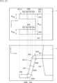
- FIG. 1 is a plan view showing an electronic device according to a first embodiment.
- FIG. 2 is a plan view of FIG. 1 in which the sealing resin is shown by imaginary lines.
- FIG. 3 is a front view of the electronic device according to the first embodiment.
- FIG. 4 is a rear view of the electronic device according to the first embodiment.
- FIG. 5 is a left side view showing the electronic device according to the first embodiment.
- FIG. 6 is a right side view showing the electronic device according to the first embodiment.
- FIG. 7 is a cross-sectional view taken along line VII-VII in FIG.
- FIG. 8 is a cross-sectional view taken along line VIII-VIII in FIG.
- FIG. 9 is an enlarged view of a main part of the electronic device according to the first embodiment, in which the upper part is an enlarged view of a part of FIG. 1 and the lower part is an enlarged view of a part of FIG.
- FIG. 10 is an enlarged view of a main part of the electronic device according to the first embodiment, in which the upper part is an enlarged view of a part of FIG. 1 and the lower part is an enlarged view of a part of FIG.
- FIG. 11 is a diagram illustrating a circuit configuration of electronic components of the electronic device according to the first embodiment.
- FIG. 12 is an enlarged plan view of a main part illustrating one process during the manufacture of the electronic device according to the first embodiment.
- FIG. 13 is a plan view showing an electronic device according to a modified example of the first embodiment, in which the sealing resin is indicated by imaginary lines.
- FIG. 14 is an enlarged view of a main part showing an electronic device according to a modified example of the first embodiment, in which the upper part is an enlarged plan view of the main part and the lower part is an enlarged side view of the main part.
- FIG. 15 is an enlarged view of a main part showing an electronic device according to a modified example of the first embodiment, in which the upper part is an enlarged plan view of the main part and the lower part is an enlarged side view of the main part.
- FIG. 14 is an enlarged view of a main part showing an electronic device according to a modified example of the first embodiment, in which the upper part is an enlarged plan view of the main part and the lower part is an enlarged side view of the main part.
- FIG. 16 is an enlarged view of a main part showing an electronic device according to another modified example of the first embodiment, in which the upper part is an enlarged plan view of the main part and the lower part is an enlarged side view of the main part.
- FIG. 17 is an enlarged view of a main part showing an electronic device according to another modification of the first embodiment, in which the upper part is an enlarged plan view of the main part and the lower part is an enlarged side view of the main part.
- FIG. 18 is an enlarged plan view of a main part of an electronic device according to another modified example of the first embodiment.
- FIG. 19 is an enlarged plan view of a main part showing an electronic device according to another modified example of the first embodiment.
- FIG. 20 is an enlarged plan view of a main part showing an electronic device according to another modified example of the first embodiment.
- FIG. 21 is a plan view showing an electronic device according to the second embodiment, in which the sealing resin is shown by imaginary lines.
- FIG. 22 is a rear view showing the electronic device according to the second embodiment.
- FIG. 23 is an enlarged view of a main part showing an electronic device according to the second embodiment, in which the upper part is an enlarged plan view of the main part and the lower part is an enlarged side view of the main part.
- FIG. 24 is an enlarged view of a main part showing an electronic device according to the second embodiment, in which the upper part is an enlarged plan view of the main part and the lower part is an enlarged side view of the main part.
- FIG. 21 is a plan view showing an electronic device according to the second embodiment, in which the sealing resin is shown by imaginary lines.
- FIG. 22 is a rear view showing the electronic device according to the second embodiment.
- FIG. 23 is an enlarged view of a main
- FIG. 25 is a plan view showing an electronic device according to a modified example of the second embodiment, in which the sealing resin is indicated by imaginary lines.
- FIG. 26 is an enlarged view of a main part showing an electronic device according to a modification of the second embodiment, in which the upper part is an enlarged plan view of the main part and the lower part is an enlarged side view of the main part.
- FIG. 27 is an enlarged view of a main part showing an electronic device according to a modification of the second embodiment, in which the upper part is an enlarged plan view of the main part and the lower part is an enlarged side view of the main part.
- FIG. 26 is an enlarged view of a main part showing an electronic device according to a modification of the second embodiment, in which the upper part is an enlarged plan view of the main part and the lower part is an enlarged side view of the main part.
- FIG. 28 is an enlarged view of a main part showing an electronic device according to another modification of the second embodiment, in which the upper part is an enlarged plan view of the main part and the lower part is an enlarged side view of the main part.
- FIG. 29 is an enlarged view of a main part showing an electronic device according to another modification of the second embodiment, in which the upper part is an enlarged plan view of the main part and the lower part is an enlarged side view of the main part.
- FIG. 30 is a plan view showing an electronic device according to the third embodiment, in which the sealing resin is shown by imaginary lines.
- FIG. 31 is a plan view showing an electronic device according to the fourth embodiment, in which the sealing resin is shown by imaginary lines.
- FIG. 32 is a diagram showing a circuit configuration of electronic components of an electronic device according to the fourth embodiment.
- FIG. 33 is a plan view showing an electronic device according to a modified example of the fourth embodiment, in which the sealing resin is indicated by imaginary lines.
- FIG. 34 is a diagram showing a circuit configuration of an electronic component of an electronic device according to the fifth embodiment.
- FIG. 35 is a diagram showing a circuit configuration of an electronic component of an electronic device according to the sixth embodiment.
- an object A is formed on an object B
- an object A is formed on (an object B)
- an object A is formed directly on an object B
- an object A is formed on an object B with another object interposed between the object A and the object B” unless otherwise specified.
- an object A is disposed on an object B” and “an object A is disposed on (an object B)” include “an object A is disposed directly on an object B” and “an object A is disposed on (an object B) with another object interposed between the object A and the object B” unless otherwise specified.
- an object A is located on (an object B) includes “an object A is in contact with an object B and is located on (an object B)” and “an object A is located on (an object B) with another object interposed between the object A and the object B".
- an object A overlaps an object B includes “an object A overlaps the entire object B” and “an object A overlaps a part of an object B” unless otherwise specified.
- an object A (its material) contains a certain material C includes “an object A (its material) is made of a certain material C” and "an object A (its material) is mainly composed of a certain material C.”
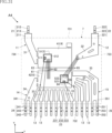
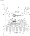
- First embodiment: 1 to 11 show an electronic device A1 according to the first embodiment.
- the electronic device A1 includes a first lead 11, a second lead 12, a plurality of third leads 13, a fourth lead 14, a fifth lead 15, a die pad 4, an electronic component 5, a plurality of connection members 61 to 66, and a sealing resin 7.
- the electronic device A1 includes eleven third leads 13, but the number of the third leads 13 is not limited.
- the specific use of the electronic device A1 is not limited in any way, but may be for detecting the battery voltage of an electric vehicle, for example.
- the electronic device A1 does not detect the battery voltage of an electric vehicle, but may detect other voltages of the electric vehicle, or may detect voltages used in industrial equipment, home appliances, or power supplies other than electric vehicles.
- the electronic device A1 is a surface-mounted semiconductor package, and in this embodiment, as shown in FIGS. 1 to 11, is an SOP (Small Outline Package) type.
- the thickness direction of electronic device A1 is referred to as "thickness direction z".
- thickness direction z the thickness direction of electronic device A1
- terms such as “top”, “bottom”, “upper”, “lower”, “top surface” and “bottom surface” indicate the relative positional relationship of each component in the thickness direction z, and do not necessarily define the relationship with the direction of gravity.
- Plant view refers to the view in the thickness direction z.
- a direction perpendicular to the thickness direction z is referred to as "first direction y”.
- a direction perpendicular to the thickness direction z and the first direction y is referred to as "second direction x”.
- the first lead 11, the second lead 12, the multiple third leads 13, the fourth lead 14, the fifth lead 15, and the die pad 4 include metals such as Cu (copper), Ni (nickel), and Fe (iron).
- the first lead 11, the second lead 12, the multiple third leads 13, the fourth lead 14, the fifth lead 15, and the die pad 4 are obtained from the same lead frame.
- the first lead 11, the second lead 12, the multiple third leads 13, the fourth lead 14, the fifth lead 15, and the die pad 4 are formed, for example, by subjecting a metal plate material to a process selected from punching, bending, etching, and the like.
- a plating layer made of Ag (silver), Ni, Au (gold), and the like may be provided at appropriate locations on each of the first lead 11, the second lead 12, the multiple third leads 13, the fourth lead 14, the fifth lead 15, and the die pad 4, as necessary.
- the first lead 11, the second lead 12, the multiple third leads 13, the fourth lead 14, and the fifth lead 15 are electrically connected to the electronic component 5 and form a conductive path in the electronic device A1.
- the first lead 11, the second lead 12, the multiple third leads 13, the fourth lead 14, and the fifth lead 15 are spaced apart from one another.
- the first lead 11, the second lead 12, the multiple third leads 13, the fourth lead 14, and the fifth lead 15 each have a portion covered by the sealing resin 7 and a portion exposed from the sealing resin 7.
- the first lead 11 includes an outer lead 21 and an outer lead 22.
- the outer lead 21 and the outer lead 22 are connected to each other and formed integrally.
- the outer lead 21 is a portion of the first lead 11 that is exposed from the sealing resin 7.
- the outer lead 21 protrudes from the sealing resin 7 in one direction in the first direction y.
- the outer lead 21 has a rectangular shape with the first direction y as its longitudinal direction.
- the outer lead 21 is bent in a gull-wing shape.
- the outer lead 21 includes a root portion 211, a mounting portion 212, an extension portion 213, and two bent portions 214, 215.
- the root portion 211 is the root part of the outer lead 21. As shown in Figures 1 and 2, the root portion 211 is located at the end of the outer lead 21 that is closer to the sealing resin 7 in the first direction y. Therefore, the root portion 211 is located closer to the sealing resin 7 in the first direction y than the mounting portion 212 and the extension portion 213. The root portion 211 is located higher in the thickness direction z than the mounting portion 212, and protrudes from the center of the sealing resin 7 in the thickness direction z.
- the mounting portion 212 is the tip portion of the outer lead 21.
- the mounting portion 212 is the portion that is joined to the circuit board when the electronic device A1 is mounted on the circuit board. As shown in Figures 1 and 2, the mounting portion 212 is located at the end opposite the sealing resin 7 in the first direction y. Therefore, the mounting portion 212 is located farther from the sealing resin 7 in the first direction y than the root portion 211 and the extension portion 213. The mounting portion 212 is located lower in the thickness direction z than the root portion 211.
- the extension portion 213 is connected to the root portion 211 via the bend portion 214 and to the mounting portion 212 via the bend portion 215.
- the extension portion 213 is inclined with respect to the root portion 211 and the mounting portion 212.
- the extension portion 213 is also inclined with respect to the thickness direction z.
- the bent portion 214 is interposed between the root portion 211 and the extending portion 213.
- the bent portion 214 is bent downward in the thickness direction z from the root portion 211.
- the bent portion 215 is interposed between the mounting portion 212 and the extending portion 213.
- the bent portion 215 is bent upward in the thickness direction z from the mounting portion 212.
- the two bent portions 214, 215 are each curved when viewed in the second direction x.
- the outer lead 21 includes a first partition 21A and a second partition 21B.
- the first partition 21A and the second partition 21B are connected to each other.
- the first partition 21A and the second partition 21B are each rectangular in a plan view.
- the first partition 21A includes a root portion 211.
- the second partition 21B includes a mounting portion 212.
- the width W 21A (dimension in the second direction x) of the first partition 21A is larger than the width W 21B (dimension in the second direction x) of the second partition 21B .
- the width W 21B is two times or more and six times or less than the width W 21A .
- the boundary 21C between the first partition 21A and the second partition 21B (hereinafter referred to as the "first partition boundary") is located between the boundary 2101 between the root portion 211 and the bent portion 214 and the central boundary 2103 of the extension portion 213.
- This central boundary 2103 of the extension portion 213 is the center in the extension direction from the bent portion 214 to the bent portion 215, and extends in the normal direction of the extension portion 213.
- the first partition boundary 21C overlaps with the boundary 2101.
- the boundary 2102 between the bent portion 214 and the extension portion 213, and the boundary 2104 between the bent portion 215 and the extension portion 213 are each parallel to the central boundary 2103.
- the first partition 21A includes a root portion 211
- the second partition 21B includes a mounting portion 212, an extension portion 213, and two bent portions 214 and 215.
- the inner lead 31 is the portion of the first lead 11 that is covered with the sealing resin 7.
- the inner lead 31 extends from the outer lead 21 inward into the sealing resin 7.
- the second lead 12 includes an outer lead 22 and an inner lead 32.
- the outer lead 22 is a portion of the second lead 12 that is exposed from the sealing resin 7.
- the outer lead 22 protrudes from the sealing resin 7 to one side in the first direction y.
- the outer lead 22 has a rectangular shape with the first direction y as its longitudinal direction.
- the plan view shape of the outer lead 22 is congruent with the plan view shape of the outer lead 21, but unlike this configuration, these plan view shapes do not have to be congruent with each other.
- the outer lead 22 is bent in a gull-wing shape when viewed in the second direction x.
- the outer lead 22 overlaps with the outer lead 21 when viewed in the second direction x.
- the outer lead 22 includes a root portion 221, a mounting portion 222, an extension portion 223, and two bent portions 224 and 225.
- the mounting portion 222 is the tip portion of the outer lead 22.
- the mounting portion 222 is a portion that is joined to the circuit board when the electronic device A1 is mounted on the circuit board. As shown in Figures 1 and 2, the mounting portion 222 is located at the end opposite the sealing resin 7 in the first direction y. Therefore, the mounting portion 222 is located farther from the sealing resin 7 in the first direction y than the root portion 221 and the extension portion 223.
- the mounting portion 222 is located lower in the thickness direction z than the root portion 221.
- the mounting portion 222 is disposed at the same position as the mounting portion 212 in the thickness direction z.
- the root portion 221 is the root part of the outer lead 22. As shown in Figures 1 and 2, the root portion 221 is located at the end of the outer lead 22 on the sealing resin 7 side in the first direction y. Therefore, the root portion 221 is located closer to the sealing resin 7 in the first direction y than the mounting portion 222 and the extension portion 223. The root portion 221 is located higher in the thickness direction z than the mounting portion 222, and protrudes from the center of the sealing resin 7 in the thickness direction z. The root portion 221 is located in the same position as the root portion 211 in the thickness direction z.
- the extension portion 223 is connected to the base portion 221 via the bend portion 224 and to the mounting portion 222 via the bend portion 225.
- the extension portion 223 is inclined with respect to the mounting portion 222 and the base portion 221 when viewed in the second direction x.
- the bent portion 224 is interposed between the root portion 221 and the extending portion 223.
- the bent portion 224 is bent downward in the thickness direction z from the root portion 221.
- the bent portion 225 is interposed between the mounting portion 222 and the extending portion 223.
- the bent portion 225 is bent upward in the thickness direction z from the mounting portion 222.
- the two bent portions 224, 225 are each curved when viewed in the second direction x.
- the outer lead 22 includes a third partition 22A and a fourth partition 22B.
- the third partition 22A and the fourth partition 22B are connected to each other.
- the third partition 22A includes a root portion 221.
- the fourth partition 22B includes a mounting portion 222.
- the width (dimension in the second direction x) W 22A of the third partition 22A is larger than the width (dimension in the second direction x) W 22B of the fourth partition 22B.
- the width W 22B is two or more times and six or less times the width W 22A .
- width W 21A of the first partition 21A and the width W 22A of the third partition 22A are the same, and the width W 21B of the second partition 21B and the width W 22B of the fourth partition 22B are the same, but they may be different.
- the boundary 22C between the third partition 22A and the fourth partition 22B (hereinafter referred to as the "second partition boundary") is located between the boundary 2201 between the root portion 221 and the bent portion 224 and the central boundary 2203 of the extension portion 223.
- This central boundary 2203 of the extension portion 223 is the center in the extension direction from the bent portion 224 to the bent portion 225, and extends in the normal direction of the extension portion 223.
- the second partition boundary 22C overlaps with the boundary 2201.
- the boundary 2202 between the bent portion 224 and the extension portion 223, and the boundary 2204 between the bent portion 225 and the extension portion 223 are each parallel to the central boundary 2203.
- the third partition 22A includes a root portion 221
- the fourth partition 22B includes a mounting portion 222, an extension portion 223, and two bent portions 224, 225.
- the inner lead 32 is the portion of the second lead 12 that is covered with the sealing resin 7.
- the inner lead 32 is connected to the outer lead 22 and extends from the outer lead 22 inward into the sealing resin 7.
- Each of the multiple third leads 13 includes an outer lead 23 and an inner lead 33.
- the electronic device A1 has multiple outer leads 23 and multiple inner leads 33.
- the outer leads 23 and inner leads 33 described below are common to each third lead 13 unless otherwise specified.
- the outer lead 23 is a portion of each third lead 13 that is exposed from the sealing resin 7. Each outer lead 23 protrudes from the sealing resin 7 to the other side in the first direction y. In a planar view, each outer lead 23 is strip-shaped with the first direction y as its longitudinal direction. The multiple outer leads 23 are arranged at equal intervals along the second direction x. Each outer lead 23 is bent in a gull-wing shape when viewed in the second direction x. The multiple outer leads 23 overlap each other when viewed in the second direction x.
- the outer lead 23 includes a root portion 231, a mounting portion 232, an extension portion 233, and two bent portions 234, 235.
- the electronic device A1 has multiple root portions 231, multiple mounting portions 232, multiple extension portions 233, and multiple bent portions 234, 235.
- the base portion 231, mounting portion 232, extension portion 233, and two bent portions 234 and 235 described below are common to each outer lead 23 unless otherwise specified.
- the mounting portion 232 is a tip portion of the outer lead 23.
- the mounting portion 232 is a portion that is joined to the circuit board when the electronic device A1 is mounted on the circuit board. As shown in FIG. 1 and FIG. 2, the mounting portion 232 is located at an end portion opposite to the sealing resin 7 in the first direction y. Therefore, the mounting portion 232 is located farther from the sealing resin 7 than the root portion 231 and the extension portion 233 in the first direction y.
- the mounting portion 232 is located lower in the thickness direction z than the root portion 231.
- the multiple mounting portions 232 are arranged at the same position in the thickness direction z.
- the multiple mounting portions 232 are arranged at equal intervals along the second direction x.
- each mounting portion 232 (dimension in the second direction x) of each mounting portion 232 (see FIG. 1) is equal to or less than the width W 21B of the second partition portion 21B and the width W 22B of the fourth partition portion 22B.
- the width W21B of the second partition portion 21B and the width W22B of the fourth partition portion 22B are each equal to or greater than the width W23 of each mounting portion 232.
- the width W23 of each mounting portion 232 is, for example, 0.15 mm or more and 0.5 mm or less.
- the root portion 231 is a root portion of the outer lead 23. As shown in FIG. 1 and FIG. 2, the root portion 231 is located at an end of the outer lead 23 on the sealing resin 7 side in the first direction y. Therefore, the root portion 231 is located closer to the sealing resin 7 than the mounting portion 232 and the extending portion 233 in the first direction y. The root portion 231 is located higher in the thickness direction z than the mounting portion 232, and protrudes from the center of the sealing resin 7 in the thickness direction z. The multiple root portions 231 are arranged at the same position as each other in the thickness direction z. The width of the root portion 231 (the dimension in the second direction x) is the same as the width W23 of the mounting portion 232.
- the extending portion 233 connects the mounting portion 232 and the root portion 231. When viewed in the second direction x, the extending portion 233 is inclined with respect to the mounting portion 232 and the root portion 231.
- the width (dimension in the second direction x) of the extending portion 233 is the same as the width W23 of the mounting portion 232.
- the bent portion 234 is interposed between the root portion 231 and the extension portion 233.
- the bent portion 234 is bent downward from the root portion 231 in the thickness direction z.
- the bent portion 235 is interposed between the mounting portion 232 and the bent portion 234.
- the bent portion 235 is bent upward from the mounting portion 232 in the thickness direction z.
- the two bent portions 234, 235 are each curved when viewed in the second direction x.
- the inner lead 33 is the portion of each third lead 13 that is covered with the sealing resin 7.
- the inner lead 33 is connected to the outer lead 23 and extends from the outer lead 23 inward into the sealing resin 7.
- the fourth lead 14 includes an outer lead 24 and an inner lead 34.
- the outer lead 24 is a portion of the fourth lead 14 that is exposed from the sealing resin 7.
- the outer lead 24 protrudes from the sealing resin 7 to the other side in the first direction y.
- the outer lead 24 is located on the other side in the second direction x relative to the multiple outer leads 23.
- the outer lead 24 is bent in a gull-wing shape when viewed in the second direction x.
- the outer lead 24 overlaps each outer lead 23 when viewed in the second direction x.
- the outer lead 24 includes multiple portions that are separated from each other. In the example shown in Figures 1 and 2, it includes two portions that are separated from each other. Each separated portion of the outer lead 24 is rectangular in plan view with the first direction y as the longitudinal direction.
- each portion is congruent with the planar shape of the outer lead 23, but unlike this configuration, these planar shapes do not have to be congruent with each other.
- Each of the separated portions of the outer lead 24 includes a root portion 241, a mounting portion 242, an extension portion 243, and two bent portions 244, 245.
- the outer lead 24 includes two root portions 241, two mounting portions 242, two extension portions 243, and multiple bent portions 244, 245.
- the root portion 241, mounting portion 242, extension portion 243, bent portion 244, and bent portion 245 described below are common to each of the separated portions of the outer lead 24 unless otherwise specified.
- the mounting portion 242 is a tip portion of each separated portion of the outer lead 24.
- the mounting portion 242 is a portion that is joined to the circuit board when the electronic device A1 is mounted on the circuit board. As shown in FIG. 1 and FIG. 2, the mounting portion 242 is located at an end portion opposite to the sealing resin 7 in the first direction y. Therefore, the mounting portion 242 is located farther from the sealing resin 7 in the first direction y than the root portion 241, the extension portion 243, and the two bent portions 244 and 245.
- the mounting portion 242 is located lower in the thickness direction z than the root portion 241.
- the mounting portion 242 is disposed at the same position as each mounting portion 232 in the thickness direction z.
- the two mounting portions 242 are adjacent to each other in the second direction x on the other side of the multiple mounting portions 232 in the second direction x.
- the width (dimension in the second direction x) W 24 of each of the two mounting portions 242 (see FIG. 1) is, for example, the same as the width W 23 of each mounting portion 232.
- the width W24 of each of the two mounting portions 242 is, for example, the same as the width W21B of the second partition portion 21B.
- the width W24 of the two mounting portions 242 is, for example, 0.15 mm or more and 1.5 mm or less.
- the interval d4 (see FIG.
- the edge of the one of the two mounting portions 242 arranged on the other side in the second direction x overlaps the edge of the first partition portion 21A on the other side in the second direction x when viewed in the first direction y.
- the edge of the one of the two mounting portions 242 arranged on one side in the second direction x overlaps the edge of the first partition portion 21A on one side in the second direction x when viewed in the first direction y.
- the root portion 241 is a root portion of each separated portion of the outer lead 24. As shown in FIG. 1 and FIG. 2, the root portion 241 is located at an end portion of each separated portion of the outer lead 24 on the sealing resin 7 side in the first direction y. Therefore, the root portion 241 is located closer to the sealing resin 7 in the first direction y than the mounting portion 242, the extending portion 243, and the two bent portions 244, 245. The root portion 241 is located higher in the thickness direction z than the mounting portion 242, and protrudes from the center of the sealing resin 7 in the thickness direction z. The root portion 241 is located at the same position as each root portion 231 in the thickness direction z. The widths (dimensions in the second direction x) of the two root portions 241 are the same as the widths W24 of the two mounting portions 242.
- the extending portion 243 is connected to the base portion 241 via a bent portion 244 and is connected to the mounting portion 242 via a bent portion 245.
- the extending portion 243 is inclined with respect to the base portion 241 and the mounting portion 242 when viewed in the second direction x.
- the width (dimension in the second direction x) of the extending portion 243 is the same as the width W24 of the base portion 241.
- the bent portion 244 is interposed between the root portion 241 and the extending portion 243.
- the bent portion 244 is bent downward in the thickness direction z from the root portion 241.
- the bent portion 245 is interposed between the mounting portion 242 and the extending portion 243.
- the bent portion 245 is bent upward in the thickness direction z from the mounting portion 242.
- the two bent portions 244, 245 are each curved when viewed in the second direction x.
- the inner lead 34 is a portion of the fourth lead 14 that is covered with the sealing resin 7.
- the inner lead 34 is connected to the outer lead 24 and extends from the outer lead 24 inwardly into the sealing resin 7.
- the inner lead 34 includes a branch portion 341.
- the branch portion 341 is disposed at the end of the inner lead 34 that is connected to the outer lead 24.
- the branch portion 341 is connected to each of the multiple root portions 241.
- the branch portions 341 branch out in the same number as the number of root portions 241. Therefore, in a configuration in which the outer lead 24 includes two root portions 241, the branch portion 341 is bifurcated. Two root portions 241 extend from each of the branched tips of the branch portion 341. Therefore, the two mounting portions 242 of the outer lead 24 are at the same potential.
- the fifth lead 15 includes an outer lead 25 and an inner lead 35.
- the outer lead 25 is a portion of the fifth lead 15 that is exposed from the sealing resin 7. As shown in FIG. 2, the outer lead 25 protrudes from the sealing resin 7 to the other side in the first direction y.
- the outer lead 25 is located on one side in the second direction x with respect to the multiple outer leads 23.
- the outer lead 25 is bent in a gull-wing shape when viewed in the second direction x.
- the outer lead 25 overlaps each outer lead 23 when viewed in the second direction x.
- the outer lead 25 includes multiple portions that are separated from each other. In the example shown in FIG. 1 and FIG. 2, it includes two portions that are separated from each other. Each separated portion of the outer lead 25 is rectangular in plan view with the first direction y as the longitudinal direction.
- each portion is congruent with the planar shape of the outer lead 23, but unlike this configuration, these planar shapes do not have to be congruent with each other.
- Each of the separated portions of the outer lead 25 includes a root portion 251, a mounting portion 252, an extension portion 253, and two bent portions 254, 255.
- the outer lead 25 includes two root portions 251, two mounting portions 252, two extension portions 253, and multiple bent portions 254, 255.
- the root portion 251, mounting portion 252, extension portion 253, bent portion 254, and bent portion 255 described below are common to each of the separated portions of the outer lead 25 unless otherwise specified.
- the mounting portion 252 is a tip portion of each separated portion of the outer lead 25.
- the mounting portion 252 is a portion that is joined to the circuit board when the electronic device A1 is mounted on the circuit board.
- the mounting portion 252 is located at an end portion opposite to the sealing resin 7 in the first direction y. Therefore, the mounting portion 252 is located farther from the sealing resin 7 in the first direction y than the root portion 251, the extension portion 253, and the two bent portions 254 and 255.
- the mounting portion 252 is located lower in the thickness direction z than the root portion 251.
- the mounting portion 252 is disposed at the same position as each mounting portion 232 in the thickness direction z.
- the two mounting portions 252 are adjacent to each other in the second direction x on one side of the multiple mounting portions 232 in the second direction x.
- the width (dimension in the second direction x) W 25 of each of the two mounting portions 252 (see FIG. 1) is, for example, the same as the width W 23 of each mounting portion 232.
- Each width W25 of the two mounting portions 252 is, for example, the same as the width W21B of the second partition portion 21B. In this embodiment, each width W25 of the two mounting portions 252 is, for example, 0.15 mm or more and 1.5 mm or less.
- the interval d5 (see FIG. 3) between the two mounting portions 252 is the same as the arrangement interval d3 between the mounting portions 232 adjacent to each other in the second direction x.
- the edge on the other side of the second direction x of the one of the two mounting portions 252 arranged on the other side of the second direction x overlaps the edge on the other side of the second direction x of the third partition portion 22A when viewed in the first direction y.
- the edge on one side of the second direction x of the one of the two mounting portions 252 arranged on one side of the second direction x overlaps the edge on one side of the second direction x of the third partition portion 22A when viewed in the first direction y.
- the root portion 251 is a root portion of each separated portion of the outer lead 25. As shown in FIG. 1 and FIG. 2, the root portion 251 is located at an end portion of each separated portion of the outer lead 25 on the sealing resin 7 side in the first direction y. Therefore, the root portion 251 is located closer to the sealing resin 7 than the mounting portion 252 and the extending portion 253 in the first direction y. The root portion 251 is located higher in the thickness direction z than the mounting portion 252 and protrudes from the center of the sealing resin 7 in the thickness direction z. The root portion 251 is located at the same position as each root portion 231 in the thickness direction z. The widths (dimensions in the second direction x) of the two root portions 251 are the same as the widths W25 of the two mounting portions 252.
- the extending portion 253 is connected to the base portion 251 via a bent portion 254 and is connected to the mounting portion 252 via a bent portion 255.
- the extending portion 253 is inclined with respect to each of the base portion 251 and the mounting portion 252.
- the width (dimension in the second direction x) of the extending portion 253 is the same as the width W25 of the base portion 251.
- the bent portion 254 is interposed between the root portion 251 and the extending portion 253.
- the bent portion 254 is bent downward in the thickness direction z from the root portion 251.
- the bent portion 255 is interposed between the mounting portion 252 and the extending portion 253.
- the bent portion 255 is bent upward in the thickness direction z from the root portion 251.
- the two bent portions 254, 255 are each curved when viewed in the second direction x.
- the inner lead 35 is a portion of the fifth lead 15 that is covered with the sealing resin 7.
- the inner lead 35 is connected to the outer lead 25 and extends from the outer lead 25 inwardly into the sealing resin 7.
- the multiple inner leads 33 are sandwiched between the two inner leads 34 and 35.
- the inner lead 35 includes a branch portion 351.
- the branch portion 351 is disposed at the end of the inner lead 35 that is connected to the outer lead 25.
- the branch portion 351 is connected to each of the multiple root portions 251.
- the branch portion 351 branches out in the same number as the number of root portions 251. Therefore, in a configuration in which the outer lead 25 includes two root portions 251, the branch portion 351 is bifurcated. Two root portions 251 extend from each of the branched tips of the branch portion 351. Therefore, the two mounting portions 252 of the outer lead 25 are at the same potential.
- mounting section 212 and mounting section 222 are adjacent to each other with a distance d12 (see FIG. 4) in the second direction x.
- Multiple mounting sections 232 are arranged with a placement distance d3 (see FIG. 3) in the second direction x.
- the placement distance d12 (see FIG. 4) in the second direction x between mounting section 212 and mounting section 222 is larger than the placement distance d3 (see FIG. 3) in the second direction x between mounting sections 232 adjacent to each other in the second direction x.
- the placement distance d12 is 10 to 20 times the placement distance d3.
- the placement distance d12 is, for example, 5 mm to 10 mm
- the placement distance d3 is, for example, 0.25 mm to 5 mm.
- the placement distance d12 is 4 mm or more.
- the distance d34 (see FIG. 3) in the second direction x between one of the two mounting sections 242 and the mounting section 232 adjacent to that mounting section 242, and the distance d35 (see FIG. 3) in the second direction x between one of the two mounting sections 252 and the mounting section 232 adjacent to that mounting section 252, are each the same as the arrangement distance d3.
- the die pad 4 supports the electronic component 5.
- the die pad 4 includes a first pad portion 41 and a second pad portion 42.
- the first pad portion 41 and the second pad portion 42 are spaced apart from each other.
- the planar shapes of the first pad portion 41 and the second pad portion 42 are not limited in any way, but in the illustrated example, they are rectangular.
- the first pad portion 41 and the second pad portion 42 are arranged, for example, in the first direction y, and the first pad portion 41 is located on one side of the second pad portion 42 in the first direction y.
- the first pad portion 41 is connected to the inner lead 31.
- the first pad portion 41 and the first lead 11 are integrally formed.
- the second pad portion 42 is connected to the two inner leads 34 and 35.
- the second pad portion 42 is integrally formed with the fourth lead 14 and the fifth lead 15.
- the shapes and positional relationships between the die pad 4 and each of the inner leads 31, 32, 33, 34, and 35 are not limited to the example shown in the figure, and can be changed as appropriate depending on the specifications of the electronic device A1.
- the electronic component 5 is an element that performs an electrical function in the electronic device A1. Although the specific function of the electronic component 5 is not limited in any way, in this embodiment, the electronic component 5 has a function of detecting voltage. In the illustrated example, the electronic component 5 includes a first chip 51 and a second chip 52 that are separated from each other.
- the first chip 51 is mounted on the first pad portion 41.
- the first chip 51 outputs to the second chip 52 a first signal corresponding to the potential of the first lead 11 and a second signal corresponding to the potential of the second lead 12.
- the first chip 51 has a plurality of electrodes 511, 512, and 513 arranged on the upper surface in the thickness direction z.
- the second chip 52 is mounted on the second pad portion 42.
- the second chip 52 receives the first and second signals from the first chip 51, and outputs a third signal according to the potential difference between the first lead 11 and the second lead 12.
- the second chip 52 outputs a detection signal (third signal) of the voltage applied between the first lead 11 and the second lead 12.
- the second chip 52 has multiple electrodes 521, 522 arranged on the upper surface in the thickness direction z.
- electronic component 5 (first chip 51 and second chip 52) has a circuit configuration, for example, as shown in FIG. 11. As shown in FIG. 11, first chip 51 includes a plurality of resistive elements R1 to R4, and second chip 52 includes an operational amplifier OP and a resistive element R5. Note that the circuit configuration of electronic component 5 is not limited to the example shown in FIG. 11.
- the two resistor elements R1 and R2 are connected in series with each other.
- the two resistor elements R1 and R2 divide the voltage of the terminal T1 (the potential difference between the potential of the terminal T1 and the reference potential of the ground GND).
- the terminal T1 corresponds to each electrode 512.
- the connection point of the two resistor elements R1 and R2 is connected to the non-inverting input terminal of the operational amplifier OP.
- the two resistor elements R3 and R4 are connected in series with each other.
- the two resistor elements R3 and R4 divide the voltage of the terminal T2 (the potential difference between the potential of the terminal T2 and the reference potential of the ground GND).
- the terminal T2 corresponds to each electrode 511.
- connection point of the two resistor elements R3 and R4 is connected to the inverting input terminal of the operational amplifier OP.
- the operational amplifier OP receives a first signal (in this embodiment, a signal obtained by dividing the voltage at terminal T1) corresponding to the potential at terminal T1 and a second signal (in this embodiment, a signal obtained by dividing the voltage at terminal T2) corresponding to the potential at terminal T2, and outputs a third signal corresponding to the potential difference between terminals T1 and T2.
- the resistive element R5 is an element (feedback resistor) for determining the amplification gain of the operational amplifier OP, and one end of the resistive element R5 is connected to the inverting input terminal of the operational amplifier OP, and the other end is connected to the output terminal of the operational amplifier OP. Note that the second chip 52 does not have to include the resistive element R5.
- the multiple connection members 61-66 each electrically connect parts spaced apart from one another.
- the multiple connection members 61-66 are each bonding wires.
- the multiple connection members 61-66 may each be a plate-shaped metal member instead of a bonding wire.
- the multiple connection members 61-66 each contain Au, Al (aluminum), or Cu.
- connection member 61 is joined to the electrode 511 of the first chip 51 and the inner lead 31, and electrically connects the first chip 51 and the first lead 11.
- the outer lead 21 of the first lead 11 is electrically connected to the first chip 51 of the electronic component 5 via the connection member 61.
- connection member 62 is joined to the first chip 51, the electrode 512, and the inner lead 32, and electrically connects the first chip 51 and the second lead 12.
- the outer lead 22 of the second lead 12 is electrically connected to the first chip 51 of the electronic component 5 via the connection member 62.
- each of the multiple connection members 63 is joined to the electrode 521 of the second chip 52 and one of the multiple inner leads 33, electrically connecting the second chip 52 to one of the multiple third leads 13.
- each outer lead 23 of the multiple third leads 13 is electrically connected to the second chip 52 of the electronic component 5 via one of the multiple connection members 63.
- connection member 64 is joined to the electrode 521 of the second chip 52 and the inner lead 34, and electrically connects the second chip 52 and the fourth lead 14.
- the outer lead 24 of the fourth lead 14 is electrically connected to the second chip 52 of the electronic component 5 via the connection member 64.
- connection member 65 is joined to the electrode 521 and the inner lead 35 of the second chip 52, and electrically connects the second chip 52 and the fifth lead 15.
- the outer lead 25 of the fifth lead 15 is electrically connected to the second chip 52 of the electronic component 5 via the connection member 65.
- the multiple connection members 66 are joined to the electrodes 513 of the first chip 51 and the electrodes 522 of the second chip 52, electrically connecting the first chip 51 and the second chip 52.
- the multiple connection members 66 are transmission paths for the first signal and the second signal.
- the sealing resin 7 covers the first lead 11, the second lead 12, the third leads 13, the fourth lead 14, and the fifth lead 15, the die pad 4 (the first pad portion 41 and the second pad portion 42), the electronic component 5 (the first chip 51 and the second chip 52), and the connection members 61 to 66.
- the sealing resin 7 includes an insulating material such as an epoxy resin.
- the sealing resin 7 is made of a resin material having a CTI (Comparative Tracking Index) of 600 V or more.
- the sealing resin 7 has a rectangular parallelepiped shape, for example.
- the dimension of the sealing resin 7 along the second direction x is, for example, 5 mm or more and 10 mm or less, and the dimension of the sealing resin 7 along the first direction y is, for example, 3 mm or more and 13 mm or less.
- the sealing resin 7 has a resin main surface 71, a resin back surface 72, and a plurality of resin side surfaces 731 to 734.
- the resin main surface 71 and the resin back surface 72 are spaced apart from each other in the thickness direction z.
- the resin main surface 71 faces one side of the thickness direction z, and the resin back surface 72 faces the other side of the thickness direction z.
- the resin main surface 71 is the upper surface of the sealing resin 7, and the resin back surface 72 is the lower surface of the sealing resin 7.
- the pair of resin side surfaces 731, 732 are spaced apart from each other in the first direction y.
- the resin side surface 731 faces one side of the first direction y, and the resin side surface 732 faces the other side of the first direction y.
- the pair of resin side surfaces 733, 734 are spaced apart from each other in the second direction x.
- the resin side surface 733 faces one side of the second direction x, and the resin side surface 734 faces the other side of the second direction x.
- the two outer leads 21 and 22 each protrude from the resin side surface 731.
- the multiple outer leads 23, 24, and 25 each protrude from the resin side surface 732.
- the outer lead 21 includes a root portion 211, a mounting portion 212, and an extending portion 213 that is connected to the root portion 211 via a bent portion 214 and to the mounting portion 212 via a bent portion 215.
- the outer lead 21 also includes a first partition portion 21A that includes the root portion 211, and a second partition portion 21B that includes the mounting portion 212.
- the width (dimension in the second direction x) W21A of the first partition portion 21A is larger than the width (dimension in the second direction x) W21B of the second partition portion 21B .
- the electronic device A1 since the first partition boundary 21C is disposed between the boundary 2101 between the root portion 211 and the bent portion 214 and the central boundary 2103 of the extending portion 213, the electronic device A1 can suppress the variation in the shape of the outer lead 21. Therefore, the electronic device A1 can suppress the bonding failure with the circuit board.
- first partition boundary 21C is located between boundary 2101 between root portion 211 and bent portion 214, and boundary 2102 between bent portion 214 and extension portion 213.
- Research by the present inventor has revealed that the variation in the shape of the outer lead 21 is smaller when first partition boundary 21C is closer to boundary 2101 than to central boundary 2103. Therefore, in electronic device A1, first partition boundary 21C is located between boundary 2101 and boundary 2102, so electronic device A1 can further suppress the variation in the shape of the outer lead 21.
- first partition boundary 21C overlaps with boundary 2101 between root portion 211 and bent portion 214, which is preferable in suppressing the variation in the shape of the outer lead 21.
- the outer lead 22 includes a root portion 221, a mounting portion 222, and an extending portion 223 that is connected to the root portion 221 via a bent portion 224 and to the mounting portion 222 via a bent portion 225.
- the outer lead 22 also includes a third partition portion 22A including the root portion 221, and a fourth partition portion 22B including the mounting portion 222.
- the width (dimension in the second direction x) W 22A of the third partition portion 22A is larger than the width (dimension in the second direction x) W 22B of the fourth partition portion 22B.
- the second partition boundary 22C between the third partition portion 22A and the fourth partition portion 22B is disposed between a boundary 2201 (see FIG.
- the electronic device A1 can suppress variation in the shape of the outer lead 22 more than when, for example, the second partition boundary 22C is positioned at the boundary 2204 (see Figure 10) between the extension portion 223 and the bent portion 225, and the boundary 2205 (see Figure 10) between the mounting portion 222 and the bent portion 225.
- second partition boundary 22C is located between boundary 2201 between root portion 221 and bent portion 224, and boundary 2202 between bent portion 224 and extension portion 223 (see FIG. 10). Therefore, electronic device A1 can further suppress variation in the shape of outer lead 22, similar to outer lead 21.
- second partition boundary 22C overlaps with boundary 2201 between root portion 221 and bent portion 224, which is preferable in suppressing variation in the shape of outer lead 22.
- the two outer leads 21, 22 are adjacent to each other in the second direction x with a distance d12 therebetween, and the multiple outer leads 23 are arranged with a spacing d3 therebetween in the second direction x.
- the spacing d12 is greater than the spacing d3.
- the variation in the shapes of the two outer leads 21, 22 tends to be greater than the variation in the shapes of the multiple outer leads 23. Therefore, as described above, arranging the first partition boundary 21C between the boundary 2101 and the central boundary 2103, and arranging the second partition boundary 22C between the boundary 2201 and the central boundary 2203 is preferable in terms of suppressing the variation in the shapes of the two outer leads 21, 22 in a package structure in which the distance d12 is greater than the arrangement distance d3.
- the first partition 21A includes a root portion 211.
- the first lead 11, the second lead 12, the multiple third leads 13, the fourth lead 14, and the fifth lead 15 are connected to one another by a tie bar 91 and are included in one lead frame 9.
- the tie bar 91 is connected to, for example, the root portion 211 of the first lead 11, the root portion 221 of the second lead 12, the root portion 231 of each third lead 13, the root portion 241 of the fourth lead 14, and the root portion 251 of the fifth lead 15.
- the inner lead 31 is supported by the tie bar 91 at a connection point C1 shown in FIG. 12. Therefore, the load of the inner lead 31 is applied to the connection point C1.
- the load on the first pad portion 41 is also applied to the connection portion C1, and the burden on the connection portion C1 becomes greater.
- a load is applied to the inner lead 31 and the first pad portion 41 when the lead frame 9 is transported, when the first chip 51 is bonded to the first pad portion 41, and when each connection member 61, 62 is bonded. If the strength of the connection portion C1 is insufficient against such a load, the first lead 11 may be deformed (for example, the connection portion C1 is bent in the direction of gravity or in the pressing direction when the first chip 51 is bonded).
- the width (dimension in the second direction x) W 21A of the first partition portion 21A is larger than the width (dimension in the second direction x) W 21B of the second partition portion 21B, so that the width of the connection portion C1 can be appropriately secured. This can improve the strength of the connection point C1 and suppress deformation of the first lead 11. That is, the electronic device A1 can suppress deformation of the first lead 11.
- the third partition 22A includes the base portion 221, and the width (dimension in the second direction x) W22A of the third partition 22A is larger than the width (dimension in the second direction x) W22B of the fourth partition 22B, so that the width of the connection point C2 (see FIG. 12) can be appropriately secured. This improves the strength of the connection point C2, so that the electronic device A1 can suppress deformation of the second lead 12.
- FIGS. 13 to 15 show an electronic device A11 according to a modified example of the first embodiment.
- the electronic device A11 differs from the electronic device A1 in the following respects. That is, in the electronic device A11, each of the outer leads 24, 25 has the same shape as the outer lead 21 (outer lead 22).
- the outer lead 24 of the electronic device A11 includes a root portion 241, a mounting portion 242, an extension portion 243, and two bent portions 244, 245. Therefore, the outer lead 24 of the electronic device A11 is not separated into multiple portions.
- the outer lead 24 of the electronic device A11 includes two partitions 24A and 24B.
- the two partitions 24A and 24B are connected to each other.
- the partition 24A includes a root portion 241.
- the partition 24B includes a mounting portion 242.
- the width (dimension in the second direction x) W 24A of the partition 24A is larger than the width (dimension in the second direction x) W 24B of the partition 24B.
- the width W 24B is between two and six times the width W 24A .
- the partition boundary 24C of the two partitions 24A, 24B is located between the boundary 2401 between the root portion 241 and the bent portion 244 and the central boundary 2403 of the extending portion 243.
- the central boundary 2403 of the extending portion 243 is the center in the extending direction from the bent portion 244 to the bent portion 245, and extends in the normal direction of the extending portion 243.
- the partition boundary 24C overlaps with the boundary 2401.
- the boundary 2402 between the bent portion 244 and the extending portion 243, and the boundary 2404 between the bent portion 245 and the extending portion 243 are each parallel to the central boundary 2403.
- the partition 24A includes the root portion 241
- the partition 24B includes the mounting portion 242, the extending portion 243, and the two bent portions 244, 245.
- the outer lead 25 of the electronic device A11 includes a root portion 251, a mounting portion 252, an extension portion 253, and two bent portions 254 and 255. Therefore, the outer lead 25 of the electronic device A11 is not separated into multiple portions.
- the outer lead 25 of the electronic device A11 includes two partitions 25A and 25B.
- the two partitions 25A and 25B are connected to each other.
- the partition 25A includes a root portion 251.
- the partition 25B includes a mounting portion 252.
- a width (dimension in the second direction x) W25A of the partition 25A is larger than a width (dimension in the second direction x) W25B of the partition 25B.
- the width W25B is greater than or equal to two times and less than or equal to six times the width W25A .
- the partition boundary 25C of the two partitions 25A and 25B is located between the boundary 2501 between the root portion 251 and the bent portion 254 and the central boundary 2503 of the extending portion 253.
- the central boundary 2503 of the extending portion 253 is the center in the extending direction from the bent portion 254 to the bent portion 255, and extends in the normal direction of the extending portion 253.
- the partition boundary 25C overlaps the boundary 2501.
- the boundary 2502 between the bent portion 254 and the extending portion 253, and the boundary 2504 between the bent portion 255 and the extending portion 253 are each parallel to the central boundary 2503.
- the partition 25A includes the root portion 251
- the partition 25B includes the mounting portion 252, the extending portion 253, and the two bent portions 254 and 255.
- electronic device A11 can suppress variation in the shape of each outer lead 21, 22.
- electronic device A11 has the same configuration as electronic device A1 and thus achieves the same effects.
- the outer lead 24 is configured similarly to the outer lead 21 (outer lead 22). Therefore, the electronic device A11 can suppress the variation in the shape of the outer lead 24 more than when, for example, the partition boundary 24C is arranged at the boundary 2404 (see FIG. 14) between the extension portion 243 and the bent portion 245 and the boundary 2405 (see FIG. 14) between the mounting portion 242 and the bent portion 245.
- the outer lead 25 is configured similarly to the outer lead 21 (outer lead 22). Therefore, the electronic device A11 can suppress the variation in the shape of the outer lead 25 more than when, for example, the partition boundary 25C is arranged at the boundary 2504 (see FIG. 15) between the extension portion 253 and the bent portion 255 and the boundary 2505 (see FIG. 15) between the mounting portion 252 and the bent portion 255.
- the first partition boundary 21C may overlap the boundary 2101 between the root portion 211 and the bent portion 214, but as described above, the first partition boundary 21C may be disposed between the boundary 2101 and the central boundary 2103.
- the first partition boundary 21C may be configured to overlap the boundary 2102 between the extension portion 213 and the bent portion 214 as shown in FIG. 16.
- the first partition boundary 21C may be configured to overlap the central boundary 2103 of the extension portion 213 as shown in FIG. 17.
- Such a configuration can be similarly applied to each of the outer leads 22, 24, and 25.
- the first partition 21A and the second partition 21B are rectangular in plan view, but at least one of the first partition 21A and the second partition 21B may be tapered in plan view.
- the second partition 21B may be tapered toward the tip of the mounting portion 212 (the edge farther from the sealing resin 7) as shown in FIG. 18.
- the first partition 21A may be tapered toward the tip of the base portion 211 (the edge farther from the sealing resin 7 and connected to the bent portion 214) as shown in FIG. 19.
- each of the first partition 21A and the second partition 21B may be tapered as shown in FIG. 20.
- the edge of the first partition 21A that contacts the second partition 21B and the edge of the second partition 21B that contacts the first partition 21A may have the same width (dimension in the second direction x). This configuration can also be applied to each of the outer leads 22, 24, and 25.
- 21 to 24 show an electronic device A2 according to the second embodiment.
- the electronic device A2 differs from the electronic device A1 in the following respects.
- the outer lead 21 includes two second partitions 21B.
- the outer lead 22 includes two fourth partitions 22B.
- two second partitions 21B extend from one first partition 21A in the first direction y in a plan view.
- the two second partitions 21B are spaced apart in the second direction x.
- Each first partition boundary 21C between the two second partitions 21B and the first partition 21A is located between the boundary 2101 between the root portion 211 and the bent portion 214 and the central boundary 2103 of the extension portion 213, and overlaps the boundary 2101 in the illustrated example.
- Each second partition 21B includes a mounting portion 212, an extension portion 213, and two bent portions 214, 215. The distance d1 (see FIG.
- the outer lead 21 includes two second partitions 21B, but may include three or more second partitions 21B.
- two fourth partitions 22B extend from one third partition 22A in the first direction y in a plan view.
- the two fourth partitions 22B are spaced apart in the second direction x.
- Each second partition boundary 22C between the two fourth partitions 22B and the third partition 22A is located between the boundary 2201 between the root portion 221 and the bent portion 224 and the central boundary 2203 of the extension portion 223, and overlaps the boundary 2201 in the illustrated example.
- Each fourth partition 22B includes a mounting portion 222, an extension portion 223, and two bent portions 224, 225. The distance d2 (see FIG.
- the outer lead 22 includes two fourth sections 22B, but may include three or more fourth sections 22B.
- electronic device A2 can suppress variation in the shape of the outer lead 21. Also, like electronic device A1, electronic device A2 can suppress variation in the shape of the outer lead 22. In addition, electronic device A2 has the same configuration as electronic device A1 and therefore achieves the same effects.
- FIGS. 25 to 27 show an electronic device A21 according to a modified example of the second embodiment.
- the electronic device A21 differs from the electronic device A2 in the following respect. That is, in the electronic device A21, each of the outer leads 24, 25 has the same shape as the outer lead 21 (outer lead 22).
- two partitions 24B extend from one partition 24A in the first direction y in a plan view.
- the two partitions 24B are spaced apart in the second direction x.
- Each partition boundary 24C between the partition 24A and the two partitions 24B is located between the boundary 2401 between the root portion 241 and the bent portion 244 and the central boundary 2403 of the extension portion 243, and overlaps with the boundary 2401 in the illustrated example.
- Each partition 24B includes a mounting portion 242, an extension portion 243, and two bent portions 244, 245.
- the distance d4 (see FIG. 25) between the two partitions 24B (mounting portion 242) in the second direction x is, for example, the same as the arrangement distance d3 described above.
- the outer lead 24 includes two partitions 24B, but may include three or more partitions 24B.
- two partitions 25B extend from one partition 25A in the first direction y in a plan view.
- the two partitions 25B are spaced apart in the second direction x.
- Each partition boundary 25C between the partition 25A and the two partitions 25B is located between the boundary 2501 between the root portion 251 and the bent portion 254 and the central boundary 2503 of the extension portion 253, and overlaps with the boundary 2501 in the illustrated example.
- Each partition 25B includes a mounting portion 252, an extension portion 253 and two bent portions 254, 255.
- the distance d5 (see FIG. 25) between the two partitions 25B (mounting portion 252) in the second direction x is, for example, the same as the arrangement distance d3 described above.
- the outer lead 25 includes two partitions 25B, but may include three or more partitions 25B.
- electronic device A21 can suppress variation in the shape of each outer lead 21, 22.
- electronic device A21 has the same configuration as electronic device A2 and therefore provides the same effects.
- each of the two outer leads 24, 25 is configured in the same manner as outer lead 21 (outer lead 22), so variation in the shape of each outer lead 24, 25 can be suppressed.
- each first partition boundary 21C overlaps with the boundary 2101 between the root portion 211 and the bent portion 214, but as described above, the first partition boundary 21C may be disposed between the boundary 2101 and the central boundary 2103.
- the first partition boundary 21C may overlap with the boundary 2102 between the extension portion 213 and the bent portion 214 as shown in FIG. 28.
- the first partition boundary 21C may overlap with the central boundary 2103 of the extension portion 213 as shown in FIG. 29.
- Such a configuration can be similarly applied to each outer lead 22, 24, 25.
- the number of second partitions 21B, the number of fourth partitions 22B, the number of partitions 24B, and the number of partitions 25B are not limited to one each, and may be multiple.
- Third embodiment 30 shows an electronic device A3 according to a third embodiment.
- the electronic device A3 differs from the electronic device A1 in that it does not include either the fourth lead 14 or the fifth lead 15.
- the external appearance of electronic device A3 is the same as that of electronic device A1. However, in electronic device A3, of the multiple third leads 13, the third leads 13 located on the furthest side and the furthest side in the second direction x are connected to the second pad portion 42.
- the electronic device A3 can suppress variation in the shape of the outer leads 21 and 22.
- the electronic device A3 has the same configuration as the electronic devices A1 and A2, and thus achieves the same effects.
- Fourth embodiment 31 and 32 show an electronic device A4 according to a fourth embodiment.
- the electronic device A4 has a different function of the electronic component 5 compared to the electronic device A1.
- the electronic component 5 of the electronic device A4 has a power conversion function, not a voltage detection function.
- the first chip 51 and the second chip 52 are each a switching element.
- the first chip 51 and the second chip 52 are each configured as an IGBT (Insulated Gate Bipolar Transistor), but instead of an IGBT, other transistors such as a MOSFET (Metal-Oxide-Semiconductor Field Effect Transistor) or a bipolar transistor may also be used.
- IGBT Insulated Gate Bipolar Transistor
- MOSFET Metal-Oxide-Semiconductor Field Effect Transistor
- the first chip 51 has three electrodes 511, 512, and 513.
- the electrode 511 is a gate
- the electrode 512 is an emitter
- the electrode 513 is a collector.
- the first chip 51 is configured, for example, in a vertical structure, with two electrodes 511 and 512 arranged on the upper surface (surface facing upward in the thickness direction z) and an electrode 513 arranged on the lower surface (surface facing downward in the thickness direction z).
- the first chip 51 is joined to the first pad portion 41 by a conductive bonding material such as solder, and the electrode 513 provided on the lower surface is conductive to the first pad portion 41 via the conductive bonding material.
- the second chip 52 has three electrodes 521, 522, and 523.
- the electrode 521 is a gate
- the electrode 522 is an emitter
- the electrode 523 is a collector.
- the second chip 52 is configured, for example, in a vertical structure, with two electrodes 521 and 522 arranged on the upper surface (surface facing upward in the thickness direction z) and an electrode 523 arranged on the lower surface (surface facing downward in the thickness direction z).
- the second chip 52 is joined to the second pad portion 42 by a conductive bonding material such as solder, and the electrode 523 provided on the lower surface is conductive to the second pad portion 42 via the conductive bonding material.
- the first chip 51 and the second chip 52 may have a horizontal structure instead of a vertical structure.
- the electrode 513 is disposed on the upper surface of the first chip 51
- the electrode 523 is disposed on the upper surface of the second chip 52.
- the electrode 513 and the first pad portion 41 (which may be the inner lead 31) are electrically connected by a bonding wire or a plate-shaped metal member
- the electrode 523 and the second pad portion 42 (which may be the inner lead 34 or the inner lead 35) are electrically connected by a bonding wire or a plate-shaped metal member.
- connection member 61 is joined to the electrode 511 and one of the inner leads 33 of the multiple third leads 13, electrically connecting them.
- the mounting portion 232 of the third lead 13 to which the connection member 61 is joined is a signal input terminal that inputs a drive signal for the first chip 51.
- the multiple connection members 62 are joined to the electrode 512 and the second pad portion 42, electrically connecting them.
- the connection member 63 is joined to the electrode 512 and one of the inner leads 33 of the multiple third leads 13, electrically connecting them.
- the mounting portion 232 of the third lead 13 to which the connection member 63 is joined is a detection terminal for detecting a current flowing through the first chip 51.
- connection member 64 is joined to the electrode 521 and one of the inner leads 33 of the multiple third leads 13, electrically connecting them.
- the mounting portion 232 of the third lead 13 to which the connection member 64 is joined is a signal input terminal that inputs a drive signal for the second chip 52.
- the multiple connection members 65 are joined to the electrode 522 and the inner lead 32 of the second lead 12, electrically connecting them.
- the connection member 66 is joined to the electrode 522 and any of the inner leads 33 of the multiple third leads 13, electrically connecting them.
- the mounting portion 232 of the third lead 13 to which the connection member 66 is joined is a detection terminal for detecting the current flowing through the second chip 52.
- a power supply voltage (e.g., DC voltage) is applied to the outer leads 21 and 22, and the power supply voltage is converted to a predetermined voltage (e.g., AC voltage) by the switching operations of the first chip 51 and the second chip 52. This converted voltage is output from the two outer leads 24 and 25.
- a predetermined voltage e.g., AC voltage
- the electronic device A4 can suppress variation in the shape of each of the outer leads 21, 22.
- the electronic device A4 has the same configuration as each of the electronic devices A1 to A3, and thus achieves the same effects.
- FIG. 33 shows an electronic device A41 according to a modification of the fourth embodiment.
- the second chip 52 of the electronic device A41 is not a switching element, but a control IC that controls the driving of the first chip 51. This modification also achieves the same effects as the electronic device A4.
- the function of the electronic component 5 is not limited to a voltage detection function.
- the electronic component 5 (first chip 51 and second chip 52) includes a semiconductor element made of a semiconductor material.
- Fig. 34 shows an electronic device A5 according to a fifth embodiment.
- the electronic device A5 differs from the electronic device A1 in that a first chip 51 and a second chip 52 are mounted on one pad portion (pad portion 40 described below).
- die pad 4 includes one pad portion 40.
- a first chip 51 and a second chip 52 are mounted on pad portion 40.
- pad portion 40 (die pad 4) is spaced apart from first lead 11, second lead 12, and multiple third leads 13, and is connected to fourth lead 14 and fifth lead 15.
- the outer lead 21 includes mutually separated portions, and each of the separated portions includes a root portion 211, a mounting portion 212, an extension portion 213, and two bent portions 214, 215.
- the widths (dimensions in the second direction x) of the root portion 211, the mounting portion 212, the extension portion 213, and the two bent portions 214, 215 are the same for each of the separated portions of the outer lead 21.
- the outer lead 22 includes mutually separated portions, and each of the separated portions includes a root portion 221, a mounting portion 222, an extension portion 223, and two bent portions 224, 225.
- the widths (dimensions in the second direction x) of the root portion 221, the mounting portion 222, the extension portion 223, and the two bent portions 224, 225 are the same for each of the separated portions of the outer lead 22.
- electronic device A5 similar to electronic devices A11 and A21, the variation in the shape of each outer lead 24, 25 can be suppressed.
- electronic device A5 has the same configuration as electronic devices A1 to A4, A11, A21, and A41, and thus achieves the same effects.
- the configuration of the die pad 4 is not limited to a configuration including a first pad portion 41 and a second pad portion 42. In other words, in the electronic device of the present disclosure, there is no limitation as to whether or not the die pad 4 is divided into a plurality of pad portions.
- Sixth embodiment: 35 shows an electronic device A6 according to a sixth embodiment.
- the electronic device A6 differs from the electronic device A5 in that the electronic component 5 is composed of a single chip 50.
- the chip 50 includes, for example, a first functional unit 501 and a second functional unit 502.
- the chip 50 is a chip in which the first functional unit 501 and the second functional unit 502 are integrated.
- the functions of the first functional unit 501 and the second functional unit 502 are not limited in any way, but for example, the first functional unit 501 has a function of outputting a signal corresponding to the potential of the outer lead 21 and a signal corresponding to the potential of the outer lead 22, similar to the first chip 51 of the electronic device A1, and the second functional unit 502 has a function of outputting a signal corresponding to the potential difference between the two outer leads 21 and 22, similar to the second chip 52 of the electronic device A1.
- the first functional unit 501 may have a switching function similar to the first chip 51 of the electronic device A3, and the second functional unit 502 may have a switching function similar to the second chip 52 of the electronic device A3.
- the first functional unit 501 and the second functional unit 502 are electrically connected to each other, for example, by internal wiring (not shown) of the chip 50.
- electronic device A6 like electronic device A5, the variation in the shape of each outer lead 24, 25 can be suppressed.
- electronic device A6 has the same configuration as electronic devices A1 to A5, A11, A21, and A41, and thus achieves the same effects.
- the electronic component 5 is not limited to a configuration including a first chip 51 and a second chip 52. In other words, in the electronic device of the present disclosure, there is no limitation as to whether or not the electronic component 5 includes multiple chips.
- first to sixth embodiments an example was shown in which two or more of the multiple outer leads 21, 22, 24, 25 include two partitions with different widths (first partition 21A and second partition 21B, third partition 22A and fourth partition 22B, partition 24A and partition 24B, partition 25A and partition 25B).
- first partition 21A and second partition 21B third partition 22A and fourth partition 22B, partition 24A and partition 24B, partition 25A and partition 25B.
- only one of the multiple outer leads 21, 22, 24, 25 may be configured to include two partitions with different widths.
- one of the multiple outer leads 21, 22, 24, 25 with the largest shape variation may be configured to include two partitions with different widths.
- the electronic device according to the present disclosure is not limited to the above-described embodiment.
- the specific configuration of each part of the electronic device according to the present disclosure can be freely designed in various ways.
- the present disclosure includes the embodiments described in the following appendices. Appendix 1.
- a sealing resin that covers the electronic component and has a first resin side surface facing one side of a first direction perpendicular to a thickness direction
- an outer lead including: a base portion extending in the first direction from the first resin side surface; a mounting portion located on one side of the base portion in the thickness direction; and an extension portion connected to the base portion via a first bent portion and connected to the mounting portion via a second bent portion; Equipped with the outer lead includes a first partition including the base portion, and a second partition including the mounting portion and connected to the first partition, a dimension of the first partition in the thickness direction and in a second direction perpendicular to the first direction is larger than a dimension of the second partition in the second direction; an electronic device, wherein a first partition boundary between the first partition and the second partition is located between a first boundary between the root portion and the first bent portion and a center of the extension portion in an extension direction from the first bent portion to the second bent portion.
- Appendix 2 The electronic device of claim 1, wherein the first partition boundary is located between the first boundary and a second boundary between the first bend portion and the extension portion. Appendix 3. 3. The electronic device of claim 2, wherein the first partition boundary overlaps the first boundary. Appendix 4. 4. The electronic device according to claim 1, wherein the extension is inclined with respect to the thickness direction when viewed in the second direction. Appendix 5. the outer lead includes an additional second section; 5. The electronic device according to claim 1, wherein the two second partitions are spaced apart in the second direction. Appendix 6. The outer lead is a first outer lead, and a second outer lead is further provided. 6.
- the second outer lead is disposed on one side in the second direction relative to the first outer lead and protrudes from the first resin side surface.
- Appendix 7. The electronic device of claim 6, wherein the entire second outer lead overlaps the entire first outer lead when viewed in the second direction.
- Appendix 8. the second outer lead includes a third partition portion extending in the first direction from the first resin side surface and a fourth partition portion connected to the third partition portion; a dimension of the third partition in the second direction is larger than a dimension of the fourth partition in the second direction; 8.
- a second partition boundary between the third partition and the fourth partition overlaps with the first partition boundary when viewed in the first direction. Appendix 9.
- the sealing resin has a second resin side surface facing an opposite side to the first resin side surface in the first direction, 9.
- each of the third outer leads protrudes from the second resin side surface.
- Appendix 10. the third outer leads are arranged at equal intervals in the second direction, 10. The electronic device of claim 9, wherein the distance between the first outer lead and the second outer lead in the second direction is greater than the arrangement distance between the third outer leads in the second direction.
- Appendix 11. The electronic device described in Appendix 9 or Appendix 10, wherein each of the multiple third outer leads has the same width in the second direction from a base end closer to the sealing resin in the first direction to a tip end farther from the sealing resin in the first direction.
- the sealing resin has a resin back surface facing the one side in the thickness direction, 18.
- the mounting portion overlaps the back surface of the resin when viewed in the first direction.
Landscapes
- Structures Or Materials For Encapsulating Or Coating Semiconductor Devices Or Solid State Devices (AREA)
- Physics & Mathematics (AREA)
- Geometry (AREA)
Priority Applications (2)
| Application Number | Priority Date | Filing Date | Title |
|---|---|---|---|
| JP2024554397A JPWO2024095795A1 (https=) | 2022-11-01 | 2023-10-20 | |
| US19/189,854 US20250266332A1 (en) | 2022-11-01 | 2025-04-25 | Electronic device |
Applications Claiming Priority (2)
| Application Number | Priority Date | Filing Date | Title |
|---|---|---|---|
| JP2022175672 | 2022-11-01 | ||
| JP2022-175672 | 2022-11-01 |
Related Child Applications (1)
| Application Number | Title | Priority Date | Filing Date |
|---|---|---|---|
| US19/189,854 Continuation US20250266332A1 (en) | 2022-11-01 | 2025-04-25 | Electronic device |
Publications (1)
| Publication Number | Publication Date |
|---|---|
| WO2024095795A1 true WO2024095795A1 (ja) | 2024-05-10 |
Family
ID=90930256
Family Applications (1)
| Application Number | Title | Priority Date | Filing Date |
|---|---|---|---|
| PCT/JP2023/037986 Ceased WO2024095795A1 (ja) | 2022-11-01 | 2023-10-20 | 電子装置 |
Country Status (3)
| Country | Link |
|---|---|
| US (1) | US20250266332A1 (https=) |
| JP (1) | JPWO2024095795A1 (https=) |
| WO (1) | WO2024095795A1 (https=) |
Citations (4)
| Publication number | Priority date | Publication date | Assignee | Title |
|---|---|---|---|---|
| JPH06350003A (ja) * | 1993-06-14 | 1994-12-22 | Hitachi Ltd | リードフレームおよびそれを用いた半導体集積回路装置 |
| JPH09275174A (ja) * | 1996-04-05 | 1997-10-21 | Toko Inc | 電子部品 |
| JP2016018821A (ja) * | 2014-07-04 | 2016-02-01 | 新電元工業株式会社 | 半導体装置の製造方法、半導体装置、及び、リードフレーム |
| JP2022055599A (ja) * | 2020-09-29 | 2022-04-08 | ローム株式会社 | 半導体装置 |
-
2023
- 2023-10-20 JP JP2024554397A patent/JPWO2024095795A1/ja active Pending
- 2023-10-20 WO PCT/JP2023/037986 patent/WO2024095795A1/ja not_active Ceased
-
2025
- 2025-04-25 US US19/189,854 patent/US20250266332A1/en active Pending
Patent Citations (4)
| Publication number | Priority date | Publication date | Assignee | Title |
|---|---|---|---|---|
| JPH06350003A (ja) * | 1993-06-14 | 1994-12-22 | Hitachi Ltd | リードフレームおよびそれを用いた半導体集積回路装置 |
| JPH09275174A (ja) * | 1996-04-05 | 1997-10-21 | Toko Inc | 電子部品 |
| JP2016018821A (ja) * | 2014-07-04 | 2016-02-01 | 新電元工業株式会社 | 半導体装置の製造方法、半導体装置、及び、リードフレーム |
| JP2022055599A (ja) * | 2020-09-29 | 2022-04-08 | ローム株式会社 | 半導体装置 |
Also Published As
| Publication number | Publication date |
|---|---|
| US20250266332A1 (en) | 2025-08-21 |
| JPWO2024095795A1 (https=) | 2024-05-10 |
Similar Documents
| Publication | Publication Date | Title |
|---|---|---|
| US9659912B2 (en) | Low-inductance circuit arrangement comprising load current collecting conductor track | |
| JP4459883B2 (ja) | 半導体装置 | |
| USRE43663E1 (en) | Semiconductor device | |
| CN114175234B (zh) | 半导体装置及电子装置 | |
| JP2013258321A (ja) | 半導体装置 | |
| US9029993B2 (en) | Semiconductor device including semiconductor chip mounted on lead frame | |
| WO2020021843A1 (ja) | 半導体装置 | |
| CN113380774B (zh) | 功率半导体模块 | |
| US20240332138A1 (en) | Electronic device | |
| US20250006621A1 (en) | Electronic device | |
| WO2024095795A1 (ja) | 電子装置 | |
| US10490489B2 (en) | Conductive clip connection arrangements for semiconductor packages | |
| JP4695041B2 (ja) | 半導体装置 | |
| US20260130297A1 (en) | Electronic device | |
| US20240332137A1 (en) | Electronic device | |
| CN118525371A (zh) | 电子装置 | |
| WO2025009349A1 (ja) | 電子装置 | |
| US8154874B2 (en) | Use of flexible circuits in a power module for forming connections to power devices | |
| US20250293126A1 (en) | Electronic device | |
| US20240243100A1 (en) | Semiconductor device | |
| US20260096451A1 (en) | Electronic device | |
| JP2026006865A (ja) | 半導体装置及び電気機器 | |
| WO2025158868A1 (ja) | 半導体装置 | |
| WO2023153188A1 (ja) | 半導体装置 | |
| CN120820747A (zh) | 在第一端子和第二端子之间具有分流器的电子部件 |
Legal Events
| Date | Code | Title | Description |
|---|---|---|---|
| 121 | Ep: the epo has been informed by wipo that ep was designated in this application |
Ref document number: 23885557 Country of ref document: EP Kind code of ref document: A1 |
|
| WWE | Wipo information: entry into national phase |
Ref document number: 2024554397 Country of ref document: JP |
|
| NENP | Non-entry into the national phase |
Ref country code: DE |
|
| 122 | Ep: pct application non-entry in european phase |
Ref document number: 23885557 Country of ref document: EP Kind code of ref document: A1 |