WO2024095583A1 - 積層セラミックコンデンサ - Google Patents
積層セラミックコンデンサ Download PDFInfo
- Publication number
- WO2024095583A1 WO2024095583A1 PCT/JP2023/031211 JP2023031211W WO2024095583A1 WO 2024095583 A1 WO2024095583 A1 WO 2024095583A1 JP 2023031211 W JP2023031211 W JP 2023031211W WO 2024095583 A1 WO2024095583 A1 WO 2024095583A1
- Authority
- WO
- WIPO (PCT)
- Prior art keywords
- layer
- ceramic capacitor
- laminate
- multilayer ceramic
- side margin
- Prior art date
- Legal status (The legal status is an assumption and is not a legal conclusion. Google has not performed a legal analysis and makes no representation as to the accuracy of the status listed.)
- Ceased
Links
Images


Classifications
-
- H—ELECTRICITY
- H01—ELECTRIC ELEMENTS
- H01G—CAPACITORS; CAPACITORS, RECTIFIERS, DETECTORS, SWITCHING DEVICES, LIGHT-SENSITIVE OR TEMPERATURE-SENSITIVE DEVICES OF THE ELECTROLYTIC TYPE
- H01G4/00—Fixed capacitors; Processes of their manufacture
- H01G4/002—Details
- H01G4/018—Dielectrics
- H01G4/06—Solid dielectrics
- H01G4/08—Inorganic dielectrics
- H01G4/12—Ceramic dielectrics
- H01G4/1209—Ceramic dielectrics characterised by the ceramic dielectric material
- H01G4/1218—Ceramic dielectrics characterised by the ceramic dielectric material based on titanium oxides or titanates
- H01G4/1227—Ceramic dielectrics characterised by the ceramic dielectric material based on titanium oxides or titanates based on alkaline earth titanates
-
- H—ELECTRICITY
- H01—ELECTRIC ELEMENTS
- H01G—CAPACITORS; CAPACITORS, RECTIFIERS, DETECTORS, SWITCHING DEVICES, LIGHT-SENSITIVE OR TEMPERATURE-SENSITIVE DEVICES OF THE ELECTROLYTIC TYPE
- H01G4/00—Fixed capacitors; Processes of their manufacture
- H01G4/002—Details
- H01G4/005—Electrodes
- H01G4/012—Form of non-self-supporting electrodes
-
- H—ELECTRICITY
- H01—ELECTRIC ELEMENTS
- H01G—CAPACITORS; CAPACITORS, RECTIFIERS, DETECTORS, SWITCHING DEVICES, LIGHT-SENSITIVE OR TEMPERATURE-SENSITIVE DEVICES OF THE ELECTROLYTIC TYPE
- H01G4/00—Fixed capacitors; Processes of their manufacture
- H01G4/002—Details
- H01G4/018—Dielectrics
- H01G4/06—Solid dielectrics
- H01G4/08—Inorganic dielectrics
- H01G4/12—Ceramic dielectrics
- H01G4/1209—Ceramic dielectrics characterised by the ceramic dielectric material
- H01G4/1236—Ceramic dielectrics characterised by the ceramic dielectric material based on zirconium oxides or zirconates
-
- H—ELECTRICITY
- H01—ELECTRIC ELEMENTS
- H01G—CAPACITORS; CAPACITORS, RECTIFIERS, DETECTORS, SWITCHING DEVICES, LIGHT-SENSITIVE OR TEMPERATURE-SENSITIVE DEVICES OF THE ELECTROLYTIC TYPE
- H01G4/00—Fixed capacitors; Processes of their manufacture
- H01G4/002—Details
- H01G4/224—Housing; Encapsulation
-
- H—ELECTRICITY
- H01—ELECTRIC ELEMENTS
- H01G—CAPACITORS; CAPACITORS, RECTIFIERS, DETECTORS, SWITCHING DEVICES, LIGHT-SENSITIVE OR TEMPERATURE-SENSITIVE DEVICES OF THE ELECTROLYTIC TYPE
- H01G4/00—Fixed capacitors; Processes of their manufacture
- H01G4/002—Details
- H01G4/228—Terminals
- H01G4/232—Terminals electrically connecting two or more layers of a stacked or rolled capacitor
-
- H—ELECTRICITY
- H01—ELECTRIC ELEMENTS
- H01G—CAPACITORS; CAPACITORS, RECTIFIERS, DETECTORS, SWITCHING DEVICES, LIGHT-SENSITIVE OR TEMPERATURE-SENSITIVE DEVICES OF THE ELECTROLYTIC TYPE
- H01G4/00—Fixed capacitors; Processes of their manufacture
- H01G4/30—Stacked capacitors
Definitions
- the present invention relates to a multilayer ceramic capacitor.
- Patent Documents 1 and 2 describe a method of retrofitting a side margin to ensure insulation around the internal electrodes in a laminated chip with the internal electrodes exposed on the side surfaces. This makes it possible to make the side margin thinner, and the intersection area of the internal electrodes can be made relatively large.
- the objective of the present invention is to provide a multilayer ceramic capacitor that can improve the moisture resistance reliability.
- the multilayer ceramic capacitor of the present invention is a multilayer ceramic capacitor comprising a laminate including an inner layer portion in which dielectric layers and internal electrode layers are alternately laminated, the laminate having a pair of main surfaces facing each other in the lamination direction, a pair of end faces facing each other in a length direction perpendicular to the lamination direction, and a pair of side surfaces facing each other in a width direction perpendicular to both the lamination direction and the length direction, and a pair of external electrodes respectively disposed on each of the end faces and connected to the internal electrode layer, the laminate having a pair of side margin portions respectively disposed on both sides of the inner layer portion in the width direction, and a pair of outer layer portions respectively disposed on both sides of the inner layer portion in the lamination direction and sandwiched between each of the side margin portions.
- the pair of side surfaces are a first side surface and a second side surface
- the pair of side margin portions are a first side margin portion arranged on the first side surface and a second side margin portion arranged on the second side surface
- the first cover region is made of an inorganic material and arranged on the outer surface of the laminate so as to straddle the boundary between the first side margin portion and each of the outer layer portions
- the second cover region is made of an inorganic material and arranged on the outer surface of the laminate so as to straddle the boundary between the second side margin portion and each of the outer layer portions
- each of the end faces has an uncovered portion that is not covered by either the first cover region or the second cover region, and each of the uncovered portions is connected to each of the external electrodes.
- moisture can penetrate into the multilayer ceramic capacitor through the boundaries between each side margin portion and each of the outer layer portions, improving the moisture resistance reliability of the multilayer ceramic capacitor.
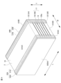
- FIG. 1 is a schematic perspective view of a multilayer ceramic capacitor.
- 2 is a cross-sectional view of the multilayer ceramic capacitor taken along line II-II in FIG. 3 is a cross-sectional view of the multilayer ceramic capacitor taken along line III-III in FIG.
- FIG. 2 is a schematic perspective view of a laminate with a cover region provided thereon.
- 1A to 1C are diagrams illustrating a manufacturing process of a multilayer ceramic capacitor.
- 1A to 1C are diagrams illustrating a manufacturing process of a multilayer ceramic capacitor.
- 1A to 1C are diagrams illustrating a manufacturing process of a multilayer ceramic capacitor.
- 3 is a diagram corresponding to FIG. 2 and illustrating a configuration of a multilayer ceramic capacitor according to a modified example of the present invention.
- FIG. 1 is a schematic perspective view of a multilayer ceramic capacitor.
- the multilayer ceramic capacitor 1 has a substantially rectangular parallelepiped shape and includes a laminate 2 and a pair of external electrodes 3 provided on both ends of the laminate 2 .
- the terms used to indicate the orientation of the multilayer ceramic capacitor 1 are the length direction L, which is the direction in which the pair of external electrodes 3 are provided in the multilayer ceramic capacitor 1.
- the direction in which the dielectric layers 14 and the internal electrode layers 15 are stacked is the stacking direction T.
- the direction that intersects both the length direction L and the stacking direction T is the width direction W. Note that in this embodiment, the width direction W is perpendicular to both the length direction L and the stacking direction T.
- a pair of outer surfaces facing in the stacking direction T are referred to as two main surfaces A
- a pair of outer surfaces facing in the width direction W are referred to as two side surfaces B
- a pair of outer surfaces facing in the length direction L are referred to as two end surfaces C.
- the two main surfaces A one is referred to as the first main surface AA
- the other is referred to as the second main surface AB (see FIG. 2).
- the two end surfaces C one is referred to as the first end surface CA, and the other is referred to as the second end surface CB.
- first main surface AA and the second main surface AB When it is not necessary to distinguish between the first main surface AA and the second main surface AB, they will be collectively referred to as the main surface A.
- first end surface CA and the second end surface CB When it is not necessary to distinguish between the first end surface CA and the second end surface CB, they will be collectively referred to as the end surface C.
- the laminate 2 includes a laminate chip 10 and a side margin portion 20.
- the laminate 2 has a rectangular parallelepiped shape. It is preferable that the corners and ridges of the laminate 2 are rounded. The corners are portions where three surfaces of the laminate intersect, and the ridges are portions where two surfaces of the laminate intersect.
- the laminate chip 10 includes an inner layer portion 11 and outer layer portions 12 disposed on both principal surface A sides of the inner layer portion 11.
- the outer layer portions 12 the one disposed on the first principal surface AA side is referred to as a first outer layer portion 12A, and the one disposed on the second principal surface AB side is referred to as a second outer layer portion 12B.
- the first outer layer portion 12A and the second outer layer portion 12B will be collectively referred to as the "outer layer portion 12.”
- the inner layer portion 11 is configured by laminating a plurality of dielectric layers 14 and a plurality of internal electrode layers 15 .
- the dielectric layer 14 is made of a ceramic material, more specifically, a dielectric ceramic material.
- the dielectric layer 14 includes ceramic particles.
- the ceramic particles are particles (main crystal particles) that are the main component of the dielectric layer 14, and are made of a compound having a perovskite structure containing Ba and/or Ti. That is, the dielectric layer 14 is a sintered polycrystalline body whose main component is a compound having a perovskite structure.
- the dielectric layer 14 may contain components other than the main component as additives.
- the additive is, for example, at least one element selected from the group consisting of Si, Mg, Ba, and Mn. In the dielectric layer 14, the additive is, for example, present between each ceramic particle.
- the thickness of the dielectric layer 14 is preferably 0.2 ⁇ m or more and 0.8 ⁇ m or less, and more preferably 0.2 ⁇ m or more and 0.55 ⁇ m or less. This allows the number of layers to be increased even for laminates 2 of the same size, ensuring sufficient capacitance.
- the internal electrode layer 15 includes a plurality of first internal electrode layers 15A and a plurality of second internal electrode layers 15B.
- the first internal electrode layers 15A and the second internal electrode layers 15B are arranged alternately. Note that the first internal electrode layers 15A and the second internal electrode layers 15B will be collectively referred to as the internal electrode layers 15 unless there is a need to distinguish between them.
- the internal electrode layer 15 is preferably formed from a metal material such as Ni, Cu, Ag, Pd, Ag-Pd alloy, Au, etc.
- the first internal electrode layer 15A has a first opposing portion 152a that faces the second internal electrode layer 15B, and a first lead portion 151a that is led out from the first opposing portion 152a to the first end face CA side.
- the end of the first lead portion 151a is exposed at the first end face CA and is electrically connected to the first external electrode 3A described below.
- the second internal electrode layer 15B has a second opposing portion 152b that faces the first internal electrode layer 15A, and a second extension portion 151b that is extended from the second opposing portion 152b to the second end face CB.
- the end of the second extension portion 151b is electrically connected to the second external electrode 3B described below.
- each end of the internal electrode layer 15 on the first side BA side is flush with the surface of the first side BA side of the inner layer 11.
- Each end of the internal electrode layer 15 on the second side BB side is flush with the surface of the second side BB side of the inner layer 11.
- each of the internal electrode layers 15 is preferably 0.2 ⁇ m or more and 2.0 ⁇ m or less, and more preferably 0.2 ⁇ m or more and 0.5 ⁇ m or less. This allows the number of layers to be increased even for laminates 2 of the same size, ensuring sufficient capacitance. In addition, the number of internal electrode layers 15 is preferably 15 or more and 1000 or less.
- the outer layer portion 12 can be made of a dielectric ceramic material.
- the outer layer portion 12 may be made of the same dielectric ceramic material as the dielectric layer 14 of the inner layer portion 11, or may be made of a dielectric ceramic material different from that of the dielectric layer 14 of the inner layer portion 11.
- the thickness of the outer layer portion 12 is set to be 15 ⁇ m or more and 60 ⁇ m or less.
- the outer layer portions 12 may each have a multi-layer structure. Furthermore, when the outer layer portions 12 contain Si, the outer layer portions 12 may have a segregated portion of Si. In such cases, it is preferable that, of the multiple layers constituting one outer layer portion 12, the layer located further away from the inner layer portion 11 has more segregated portions of Si than the layer located closest to the inner layer portion 11. This can improve the flexural strength of the multilayer ceramic capacitor 1 in the stacking direction T.
- the total number of dielectric layers 14, internal electrode layers 15, and outer layers 12 is preferably, for example, 15 or more and 1,000 or less.
- the side margin portion 20 can be made of a dielectric ceramic material.
- the side margin portion 20 may be made of the same dielectric ceramic material as the dielectric layer 14 of the inner layer portion 11, or may be made of a dielectric ceramic material different from that of the dielectric layer 14 of the inner layer portion 11.
- the side margin portion 20 is provided on both side surfaces B of the portion where the inner layer portion 11 and the outer layer portion 12 are laminated.
- the side margin portion 20 sandwiches the outer layer portion 12 in the lamination direction T.
- the side margin portion 20 covers the ends of the internal electrode layer 15 exposed on both side surfaces of the laminate chip 10 on the width direction W side along the ends.
- the side margin portion 20 that is disposed on the first side BA side is referred to as the first side margin portion 20A
- the side margin portion 20 that is disposed on the second side BB side is referred to as the second side margin portion 20B.
- the side margin portion 20 When there is no particular need to distinguish between the first side margin portion 20A and the second side margin portion 20B, they may be collectively referred to as the "side margin portion 20.”
- the dimension in the width direction W of the first side margin portion 20A is preferably 5 ⁇ m or more and 40 ⁇ m or less, and more preferably 5 ⁇ m or more and 20 ⁇ m or less.
- the dimension in the width direction W of the second side margin portion 20B is preferably 5 ⁇ m or more and 40 ⁇ m or less, and more preferably 5 ⁇ m or more and 20 ⁇ m or less. This allows the capacitance of the multilayer ceramic capacitor 1 to be increased while ensuring the moisture resistance reliability of the multilayer ceramic capacitor 1.
- the dimensions of the width direction W of the first side margin portion 20A and the second side margin portion 20B can be measured, for example, by observing the WT cross section of the laminate 2 exposed by polishing with a scanning electron microscope. Each value is obtained by averaging the measurements at multiple points in the stacking direction T.
- the first side margin portion 20A is composed of multiple layers, specifically, two layers (see FIG. 3).
- the first side margin portion 20A has a first inner layer 21A, which is the two layers that are closer to the inner layer portion 11, and a first outer layer 22A, which is the multiple layers that are farther away from the inner layer portion 11.
- the second side margin portion 20B is composed of multiple layers, specifically, two layers.
- the second side margin portion 20B has a second inner layer 21B that is positioned closer to the inner layer portion 11 of the two layers, and a second outer layer 22B that is positioned farther away from the inner layer portion 11 of the two layers.
- first inner layer 21A and the second inner layer 21B may be collectively referred to as the "inner layer 21" unless there is a need to distinguish between them.
- the first outer layer 22A and the second outer layer 22B may be collectively referred to as the "outer layer 22" unless there is a need to distinguish between them.
- the side margin portion 20 is not limited to a two-layer structure, but may be a single-layer structure or may be composed of three or more layers.
- the layer of the side margin portion 20 that is arranged closest to the inner layer portion 11 is defined as an inner layer
- the layer of the side that is arranged furthest from the inner layer portion 11 is defined as an outer layer.
- the first side margin portion 20A and the second side margin portion 20B may have different numbers of layers.
- the side margin portion 20 has a two-layer structure including an inner layer and an outer layer
- the difference in sinterability between the inner layer and the outer layer can be observed in a dark field using an optical microscope to confirm that it has a two-layer structure and to confirm the interface between the layers.
- the side margin portion 20 has a structure of three or more layers.
- the inner layer and the outer layer may not be recognized as a two-layer structure after sintering. Even if they cannot be recognized as a two-layer structure, they may be distinguishable as two regions based on the differences in the types of elements and the content of the elements.
- the dielectric layer 14, the outer layer portion 12, and the side margin portion 20 may contain ceramic grains. In this case, interfacial resistance occurs at the interface between the ceramic grains, and therefore the insulation resistance between the internal electrode layers 15 can be increased. As a result, the occurrence of short circuits in the multilayer ceramic capacitor 1 can be suppressed.
- Rare earth elements are preferably present at the ceramic grain interfaces.
- the presence of rare earth elements at the ceramic grain interfaces can be confirmed by elemental analysis using TEM-EDX.
- Examples of rare earth elements include La, Ce, Pr, Nd, Sm, Eu, Gd, Tb, Dy, Ho, Er, Tm, Yb, Lu, and Y.
- the presence of rare earth elements at the ceramic grain interfaces can further increase the interface resistance of the dielectric ceramic layer. This can further improve the reliability of the multilayer ceramic capacitor.
- Mg, Mn, Si, and the like may also be present.
- the rare earth is preferably present in an amount of 0.2 mol % or more and 5 mol % or less relative to 100 mol of Ti.
- the amount of rare earth can be confirmed by TEM-EDX.
- composition of Laminate 2 When the dielectric layer 14, the outer layer portion 12 and the side margin portion 20 are composed of dielectric ceramics, the composition of at least one of the dielectric ceramic layers constituting the dielectric layer 14, the dielectric ceramic layers constituting the outer layer portion 12 and the dielectric ceramic layers constituting the side margin portion 20 may be different from the composition of the other dielectric ceramic layers.
- the dielectric layer 14, the outer layer 12, and the side margin 20 all have different purposes for their placement and the characteristics required for their manufacturing method. Therefore, by making the composition of at least one of the dielectric ceramic layers constituting the dielectric layer 14, the outer layer 12, and the side margin 20 different from the composition of the others, it is possible to achieve an optimal composition according to the location where they are placed. This makes it possible to improve the reliability of the multilayer ceramic capacitor 1.
- the side margin portion 20 is composed of multiple dielectric ceramic layers
- the multiple dielectric ceramic layers that make up the side margin portion 20 may have the same composition or different compositions.
- composition of any one of the multiple dielectric ceramic layers constituting the side margin portion 20 is different from that of the dielectric layer 14, then it can be said that the composition of the side margin portion 20 is different from that of the dielectric layer 14. Also, if the composition of any one of the multiple dielectric ceramic layers constituting the side margin portion 20 is different from that of the outer layer portion 12, then it can be said that the composition of the side margin portion 20 is different from that of the outer layer portion 12.
- the dielectric ceramic layers constituting the dielectric layer 14, the dielectric ceramic layers constituting the outer layer portion 12, and the dielectric ceramic layers constituting the side margin portion 20 it is preferable that the dielectric ceramic layers having different compositions have a common main component with the other dielectric ceramic layers, but have different types of additives.
- the main component include BaTiO3 , CaTiO3 , and SrTiO3 .
- the additive elements are preferably Si, Mg, Mn, Sn, Cu, rare earth elements, Ni, and Al.
- the dielectric ceramic layers constituting the dielectric layer 14, the dielectric ceramic layers constituting the outer layer portion 12, and the dielectric ceramic layers constituting the side margin portion 20 may contain two or more types of the additive elements.
- “same composition” means that the types of elements contained in the dielectric ceramic that constitutes each dielectric ceramic layer are the same, and that the contents (molar ratios) of other elements based on Ti are all within ⁇ 0.5%. Differences in the diameter of the ceramic grains that constitute each dielectric ceramic layer and differences in porosity are not included in the differences in the composition of the dielectric ceramic layers.
- the composition of each dielectric ceramic layer can be determined by cutting the multilayer ceramic capacitor 1 to expose the dielectric ceramic layer and performing elemental analysis on the cut surface using wavelength dispersive X-ray analysis (WDX) or transmission electron microscope-energy dispersive X-ray analysis (TEM-EDX). At this time, the composition of each dielectric ceramic layer is measured at five points and the average value is calculated.
- WDX wavelength dispersive X-ray analysis
- TEM-EDX transmission electron microscope-energy dispersive X-ray analysis
- the composition of each layer is measured at five locations, and the composition obtained is multiplied by the proportion of the thickness (i.e., the dimension in the width direction W) that each layer occupies in the side margin portion 20, and the sum is the sum of these values. Note that if elemental segregation is observed near the interface with other dielectric ceramic layers or internal electrode layers 15, the locations where elemental segregation is observed are not to be measured by WDX.
- Mg is a preferred additive element to be added to the dielectric layers 14 and the outer layer portions 12.
- the Mg content in the dielectric layers 14 and the outer layer portions 12 is preferably 0.05 mol % or more and 3.0 mol % or less relative to 100 mol of Ti. This can increase the relative dielectric constant of the dielectric layers 14, thereby improving the capacitance of the multilayer ceramic capacitor 1. Note that there are cases where it is preferable for the Mg content in the dielectric layers 14 and the outer layer portions 12 to be as small as possible.
- Si is a preferred additive element to be added to the side margin portion 20.
- the Si content in the side margin portion 20 is preferably 0.05 mol% or more and 5.0 mol% or less per 100 mol of Ti.
- the Si content in the side margin portion 20 is preferably higher than the Si content in the dielectric layer 14 and the outer layer portion 12.
- Mg is a preferred additive element to be added to the side margin portion 20.
- the Mg content in the side margin portion 20 is preferably 0.05 mol% or more and 5.0 mol% or less per 100 mol of Ti.
- the Mg content in the side margin portion 20 is preferably higher than the Mg content in the dielectric layer 14 and the outer layer portion 12.
- Mn is a preferred additive element to be added to the side margin portion 20.
- the Mn content in the side margin portion 20 is preferably 0.01 mol% or more and 3.0 mol% or less per 100 mol of Ti.
- the Mn content in the side margin portion 20 is preferably higher than the Mn content in the dielectric layer 14 and the outer layer portion 12.
- elements derived from the dielectric layer 14 may be segregated in the vicinity of the interface with the dielectric layer 14.
- elements derived from the outer layer portion 12 may be segregated in the vicinity of the interface with the outer layer portion 12.
- an element originating from the dielectric layer 14 may be segregated near the interface with the dielectric layer 14.
- the segregated element is preferably Ni.
- an element originating from the outer layer 12 may be segregated near the interface with the outer layer 12.
- the segregated element is preferably Ni.
- Si is segregated near the interface with the side margin portion 20.
- a Si segregation region is formed in an area within a distance of 0.5 ⁇ m from the end portion on the side margin portion 20 side toward the center portion in the width direction W. This improves the flexural strength of the internal electrode layer 15.
- the porosity of the dielectric layer 14, the porosity of the outer layer portion 12, and the porosity of the side margin portion 20 may be the same or different from each other.
- the multilayer ceramic capacitor 1 is cut to expose the dielectric layer 14, the outer layer 12, and the side margin 20, and the cut surface is observed at 20,000x magnification using a scanning electron microscope (SEM). Photographs are taken of five areas with a field of view size of 6.3 ⁇ m x 4.4 ⁇ m, with no overlapping areas, and the ratio of the area occupied by voids to the entire field of view is calculated from each obtained SEM image by image analysis. The average of the calculated ratios over the five fields of view is taken as the void ratio.
- SEM scanning electron microscope
- the porosity of each layer is determined individually, and then the porosity of the side margin portion 20 is determined as the sum of the products of the width direction W dimension of each layer divided by the width direction W dimension of the side margin portion 20 and the porosity of each layer.
- the Si content of the outer layer 22 is greater than the Si content of the inner layer 21. This can improve the flexural strength of the side margin portion 20. In addition, the occurrence of cracks or chips in the side margin portion 20 can be suppressed, thereby improving the moisture resistance reliability of the multilayer ceramic capacitor 1.
- Si is added to the outer layer 22 so that the molar ratio of Si to 1 mole of Ti is 3.0 or more and 7.0 or less, while Si is added to the inner layer 21 so that the molar ratio of Si to 1 mole of Ti is 1.0 or more and 4.0 or less.
- the content of Ba as an additive in the inner layer 21 is greater than the content of Ba as an additive in the outer layer 22.
- the content of Ba as an additive in the outer layer 22 is also greater than the content of Ba as an additive in the dielectric layer 14. In this way, the content of Ba as an additive in the inner layer 21, the content of Ba as an additive in the outer layer 22, and the content of Ba as an additive in the dielectric layer 14 are different from one another.
- the difference in Ba content can be confirmed by TEM analysis.
- the Ba content in the inner layer 21 is adjusted so that the molar ratio of Ba to 1 mole of Ti is greater than 1.020 and less than 1.040 as a center value.
- the Ba content in the outer layer 22 is adjusted so that the molar ratio of Ba to 1 mole of Ti is greater than 1.01 and equal to or less than 1.020 as a center value.
- the Ba content in the dielectric layer 14 is adjusted so that the molar ratio of Ba to 1 mole of Ti is greater than 0.99 and less than 1.01 as a center value.
- the content of Ba as an additive in the inner layer 21 is in the range of greater than 100% and less than 140% of the content of Ba as an additive in the outer layer 22.
- the side margin portion 20 is formed so that the number of voids decreases from the inner layer portion 11 side toward the side away from the inner layer portion 11.
- the outer layer 22 has fewer voids than the inner layer 21. This makes it possible to suppress the intrusion of moisture and the like into the laminate 2 through the side margin portion 20, thereby improving the moisture resistance reliability of the multilayer ceramic capacitor 1.
- the elements contained as additives in the inner layer 21 are different from the elements contained as additives in the outer layer 22.
- the inner layer 21 can increase the adhesion between the side margin portion 20 and the inner layer portion 11, while the outer layer 22 can suppress the penetration of moisture into the multilayer ceramic capacitor 1.
- the inner layer 21 and the outer layer 22 cannot be visually distinguished. Even in such cases, the inner layer 21 and the outer layer 22 can be distinguished based on the types of elements they contain, the amount of elements they contain, etc.
- the dimension of the outer layer 22 in the width direction W is preferably larger than the dimension of the inner layer 21 in the width direction W. This allows the effect of the outer layer 22 in suppressing the penetration of moisture to be prominent.
- the outer layer 22 preferably has a width W dimension of 5 ⁇ m or more and 20 ⁇ m or less
- the inner layer 21 preferably has a width W dimension of 0.1 ⁇ m or more and 20 ⁇ m or less. This effectively improves the moisture resistance reliability of the multilayer ceramic capacitor 1 while increasing the adhesion between the side margin portion 20 and the inner layer portion 11.
- the external electrode 3 includes a first external electrode 3A provided on a first end face CA of the laminate 2, and a second external electrode 3B provided on a second end face CB of the laminate 2. Note that, unless there is a particular need to distinguish between the first external electrode 3A and the second external electrode 3B, they will be collectively described as the external electrode 3.
- the external electrode 3 covers not only the end face C, but also a portion of the main face A and the side face B on the end face C side.
- the external electrode 3 comprises a base electrode layer 31 and a plating layer 32 (see Figure 2).
- the base electrode layer 31 can include, for example, at least one of a baked layer, a conductive resin layer, and a thin film layer. Note that the base electrode layer 31 only needs to be disposed on at least the end face C, and does not need to extend onto the main face A or the side face B.
- the baked layer When the baked layer is used as the base electrode layer 31, the baked layer contains a glass component and a metal.
- the baked layer which will be described in detail later, is formed by applying and baking a conductive paste containing a conductive metal and glass.
- the glass component of the baking layer may contain an oxide containing at least one element selected from the group consisting of B, Si, Ba, Mg, Al, and Ti.
- the oxide is preferably SiO 2 , Al 2 O 3 , TiO 2 , BaO 2 , or ZrO 2.
- the glass component of the baking layer more preferably contains an oxide containing Ba or Ti, and the oxide is preferably BaO 2 or TiO 2. When the glass component contains BaO 2 or TiO 2 , the content of impurities is low and the flexibility is excellent.
- the metal of the baked layer can be, for example, at least one metal selected from the group consisting of Cu, Ni, Ag, Pd, Ag-Pd alloy, and Au.
- the portions of the baked layers that are disposed on the end faces C preferably have a thickness (dimension in the length direction L) at the center as viewed in the stacking direction T of 3 ⁇ m or more and 100 ⁇ m or less.
- the portions of the baked layer that are disposed on the main surface A preferably have a thickness at the center as viewed in the length direction L (dimension in the stacking direction T) of 3 ⁇ m or more and 70 ⁇ m or less.
- the portions of the baked layer that are disposed on the side surface B preferably have a thickness at the center as viewed in the longitudinal direction L of 3 ⁇ m or more and 70 ⁇ m or less.
- the conductive resin layer contains a metal and a thermosetting resin.
- the metal of the conductive resin layer is responsible for the electrical conductivity of the conductive resin layer.
- the metal of the conductive resin layer can be Ag, Cu, Ni, Sn, Bi, or an alloy containing these.
- the metal of the conductive resin layer can also be a metal powder with an Ag coating on the surface.
- the metal powder (base material) to be coated is preferably Cu, Ni, Sn, Bi, or an alloy containing these.
- the performance of the base electrode layer 31 can be improved due to the properties of Ag, such as low resistivity and resistance to oxidation.
- using an inexpensive metal as the base material can prevent costs from rising.
- the metal of the conductive resin layer can also be Cu or Ni that has been treated to prevent oxidation.
- the metal of the conductive resin layer can also be a metal powder with a surface coating of Si, Ni or Cu.
- the metal powder (base material) to be coated is preferably Ag, Cu, Ni, Sn, Bi or an alloy containing these.
- the metal of the conductive resin layer can be, for example, a spherical metal powder or a flat metal powder. It is preferable to use a mixture of spherical metal powder and flat metal powder as the metal of the conductive resin layer.
- Thermosetting resin gives flexibility to the conductive resin layer. This allows the conductive resin layer to function suitably as a buffer layer when the multilayer ceramic capacitor 1 is subjected to a physical shock or a shock caused by a thermal cycle. This makes it possible to suppress the occurrence of cracks in the multilayer ceramic capacitor 1.
- thermosetting resin can be any of various known thermosetting resins, such as epoxy resin, phenol resin, urethane resin, silicone resin, polyimide resin, etc.
- the thermosetting resin is preferably an epoxy resin.
- Epoxy resin has excellent heat resistance, moisture resistance, adhesion, etc., and can further improve the performance of the conductive resin layer.
- the conductive resin layer preferably contains a curing agent.
- the curing agent can be any of various known compounds such as phenolic compounds, amine compounds, acid anhydride compounds, imidazole compounds, active ester compounds, and amide-imide compounds.
- the conductive resin layer has a thickness of 10 ⁇ m or more and 150 ⁇ m or less at the thickest part of the conductive resin layer.
- the conductive resin layer may be provided directly on the laminate 2, or may be provided on the outside of a baked layer that is then provided on the laminate 2. When the conductive resin layer is provided on the outside of the baked layer, the conductive resin layer may completely cover the outside of the baked layer, or may only partially cover it.
- the conductive resin layer may be a single-layer structure or a multi-layer structure.
- the thin film layer is a layer in which metal particles are deposited.
- the thin film layer has a thickness of 1 ⁇ m or less.
- the thin film layer is formed by a thin film formation method such as sputtering or vapor deposition, which will be described in detail later.
- the plating layer 32 contains, for example, at least one metal selected from the group consisting of Cu, Ni, Sn, Ag, Pd, Ag-Pd alloy, and Au.
- the plating layer 32 has a first plating layer 321 disposed on the base electrode layer 31, and a second plating layer 332 disposed on the first plating layer 321. Note that the plating layer 32 does not have to have a two-layer structure, and may have a single-layer structure or a multi-layer structure of three or more layers.
- the first plating layer 331 is preferably a Ni plating layer. In that case, when mounting the multilayer ceramic capacitor 1 on the circuit board 50, the base electrode layer 31 can be prevented from being eroded by solder.
- the thickness of the first plating layer 331 is preferably 1 ⁇ m or more and 15 ⁇ m or less.
- the second plating layer 332 is preferably a Sn plating layer. This improves the wettability of the solder when mounting the multilayer ceramic capacitor 1 on the circuit board 50, making it easier to mount the multilayer ceramic capacitor 1.
- the thickness of the second plating layer 332 is preferably 1 ⁇ m or more and 15 ⁇ m or less.
- the multilayer ceramic capacitor 1 is provided with a cover region 4. Note that in each drawing, the cover region 4 is indicated by dot hatching.
- the cover region 4 is made of an inorganic material.
- the inorganic material that makes up the cover region 4 contains at least one element selected from the group consisting of Si, Ti, Ba, and Zr. This ensures the denseness of the cover region 4, and therefore prevents moisture and the like from penetrating the cover region 4. It is preferable that the inorganic material that makes up the cover region 4 is Si. This allows the effect of improving moisture resistance to be achieved by baking at a lower temperature.
- the coverage area 4 has a first coverage area 4A and a second coverage area 4B.
- the first coverage area 4A and the second coverage area 4B may be collectively referred to as "coverage area 4" unless there is a particular need to distinguish between them.
- the first cover area 4A is band-shaped and is arranged on the main surface A of the laminate 2 so as to straddle the boundary between the first side margin portion 20A and the outer layer portion 12, and is also arranged on the end surface C of the laminate 2 so as to straddle the boundary between the first side margin portion 20A and the inner layer portion 11.
- the first cover area 4A is annular and goes around in the length direction L (see FIG. 4).
- the first cover area 4A covers the entire boundary between the first side margin portion 20A and the outer layer portion 12.
- the first cover area 4A covers the entire boundary between the first side margin portion 20A and the inner layer portion 11.
- the second cover region 4B is band-shaped and is arranged on the outer surface of the laminate 2 so as to straddle the boundary between the second side margin portion 20B and the outer layer portion 12, and is also arranged on the end face C of the laminate 2 so as to straddle the boundary between the second side margin portion 20B and the inner layer portion 11.
- the second cover region 4B is annular and goes around in the length direction L.
- the second cover region 4B covers the entire boundary between the second side margin portion 20B and the outer layer portion 12.
- the second cover region 4B covers the entire boundary between the second side margin portion 20B and the inner layer portion 11.
- the thickness of the first cover region 4A is preferably 1 ⁇ m or more and 10 ⁇ m or less.
- the thickness of the second cover region 4B is preferably 1 ⁇ m or more and 10 ⁇ m or less. This allows the multilayer ceramic capacitor 1 to be made low-profile while improving the moisture resistance reliability of the multilayer ceramic capacitor 1.
- the first end face CA has a first uncovered portion CAa that is not covered by either the first cover area 4A or the second cover area 4B.
- the first end face CA is connected to the first external electrode 3A at the first uncovered portion CAa.
- the second end surface CB has a second uncovered portion CBa that is not covered by either the first cover area 4A or the second cover area 4B.
- the second end surface CB is connected to the second external electrode 3B at the second uncovered portion CBa.
- first uncoated portion CAa and the second uncoated portion CBa may be collectively referred to as “uncoated portion Ca" unless there is a need to distinguish between them.
- the dimension in the width direction W of the first cover region 4A is preferably 10% or more and 20% or less of the dimension in the width direction W of the laminate 2.
- the dimension in the width direction W of the second cover region 4B is preferably 10% or more and 20% or less of the dimension in the width direction W of the laminate 2. This makes it possible to improve the moisture resistance reliability of the multilayer ceramic capacitor 1 while sufficiently ensuring the connection between the end face C and the external electrode 3.
- the shape of the boundary between the cover area 4 and the laminate 2 is not particularly limited.
- the boundary between the cover area 4 and the laminate 2 may be confirmed by observing the cover area 4 and the laminate 2 with an optical microscope in a dark field. If the boundary can be confirmed, the cover area 4 may be recognized as a cover layer. On the other hand, the cover area 4 and the laminate 2 may be integrated, and the boundary between the cover area 4 and the laminate 2 may not be confirmed. In such cases, the main surface A and the side surface B of the laminate 2 are each regarded as flat surfaces, and the part protruding from these flat surfaces is determined to be the cover area 4.
- Fig. 5 to Fig. 7 are all diagrams showing the manufacturing process of the multilayer ceramic capacitor.
- the manufacturing process for the multilayer ceramic capacitor 1 includes a laminate manufacturing process, a cover area forming process, and an external electrode forming process.
- the laminate manufacturing process includes a laminate chip manufacturing process and a side margin portion forming process.
- a ceramic green sheet for lamination is prepared by forming a ceramic slurry into a sheet shape.
- the ceramic green sheet for lamination contains a ceramic raw material including a dielectric ceramic material, a binder, and a solvent.
- An additive including a rare earth may be added to the ceramic raw material.
- a conductive paste that will become the internal electrode layers is printed on the laminated ceramic green sheets.
- the conductive paste is printed on the surface of the laminated ceramic green sheets so that multiple stripes are aligned in the width direction of the stripes.
- the conductive paste can be printed by screen printing or gravure printing, for example.
- a predetermined number of ceramic green sheets that have not been printed with conductive paste are stacked.
- a predetermined number of ceramic green sheets that have been printed with conductive paste are stacked while being alternately shifted in the arrangement direction in which the multiple conductive pastes are printed side by side.
- a predetermined number of ceramic green sheets that have not been printed with conductive paste are stacked. This results in a mother laminate.
- the mother laminate is pressed.
- Methods that can be used to press the mother laminate include, for example, a rigid press and a hydrostatic press.
- the pressed mother laminate is cut into a chip shape. This results in a laminate chip 10, as shown in FIG. 5(a).
- Methods for cutting the mother laminate include, for example, press cutting, dicing, and laser cutting.
- a ceramic slurry for an inner layer is prepared for making a ceramic green sheet for an inner layer.
- the ceramic slurry for an inner layer includes a dielectric ceramic material mainly composed of BaTiO3 , a binder, and a solvent.
- the ceramic slurry for an inner layer may contain Si, which is a sintering aid.
- the ceramic slurry for an inner layer may also contain a liquid-phase type metal.
- the ceramic slurry for an inner layer may contain more rare earth elements, Mg, and Mn than the ceramic green sheet for forming the laminate chip 10.
- a ceramic slurry for an outer layer is prepared for producing a ceramic green sheet for an outer layer.
- the ceramic slurry for an outer layer contains a dielectric ceramic material mainly composed of BaTiO3 , a binder, and a solvent.
- the ceramic slurry for an outer layer may contain Si as a sintering aid.
- the amount of Si contained in the ceramic sheet for the inner layer is greater than the amount of Si contained in the ceramic sheet for the outer layer.
- the amount of Si contained in the ceramic sheet for the inner layer and the ceramic sheet for the outer layer is determined by imaging the cross sections of the ceramic sheet for the inner layer and the ceramic sheet for the outer layer by WDX and based on the area of the region where Si is detected.
- the outer layer ceramic slurry is applied to the surface of the resin film and dried. As a result, an outer layer ceramic green sheet 22a is formed on the resin film.
- the inner layer ceramic slurry is applied to the surface of the outer layer ceramic green sheet and dried. As a result, an inner layer ceramic green sheet 21a is formed on the outer layer ceramic green sheet. As a result, a side margin ceramic green sheet 20a having a two-layer structure is obtained, as shown in Figure 5 (b).
- the side margin ceramic green sheet 20a having a two-layer structure may be obtained, for example, by laminating together a preformed outer layer ceramic green sheet 22a and an inner layer ceramic green sheet 21a.
- the side margin ceramic green sheet 20a is peeled off from the resin film.
- the side margin ceramic green sheet 20a is pressed against the laminate chip 10 and punched out by the laminate chip 10 with its inner layer side surface facing the side B side surface of the laminate chip 10. This forms a side margin portion 20 in the laminate chip 10.
- the laminate 2 is obtained as shown in Figure 5 (c). It is preferable that an organic solvent that acts as an adhesive is applied to the side surface of the laminate chip 10 in advance.
- the laminate 2 is preferably subjected to barrel polishing or the like. This allows the corners and ridges of the laminate 2 to be rounded.
- the laminate 2 is degreased in a nitrogen atmosphere.
- the laminate 2 is then fired in a mixed atmosphere of nitrogen, hydrogen, and water vapor.
- the temperature at which the laminate 2 is fired is preferably, for example, 900°C or higher and 1300°C or lower.
- a paste bath filled with cover region paste P that will become the cover region 4 is prepared.
- the cover region paste P contains at least one of the inorganic materials Si, Ti, Ba, and Zr.
- the laminate 2 is dipped into the cover region paste P with the second side surface BB facing downward. At this time, a part of the laminate 2 on the second side surface BB side is dipped into the cover region paste P, and more specifically, a part of the laminate 2 that includes at least the boundary between the laminate chip 10 and the second side margin portion 20B is dipped into the cover region paste P.
- the dimension of the width direction W of the cover region 4 can be adjusted by adjusting the depth to which the laminate 2 is dipped into the cover region paste P.
- the laminate 2 is pulled up from the paste bath filled with the cover region paste P.
- the laminate 2 is in a state in which the cover region paste P is applied to the entire second side BB, a portion of the main surface A on the second side BB side, and a portion of the end surface C on the second side BB side.
- the cover region paste P is arranged so as to straddle the boundary between the second side margin portion 20B and the outer layer portion 12.
- the cover region paste P is arranged so as to straddle the boundary between the second side margin portion 20B and the inner layer portion 11.
- unnecessary cover area paste P arranged on the laminate 2 is written off.
- the cover area paste P arranged on the second side BB is written off.
- the thickness and width W dimensions of the cover area 4 are adjusted to the desired dimensions. Note that writing off the cover area paste P is not essential and may be performed as necessary.
- the cover area paste P is dried to become the second cover area 4B.
- the drying temperature and drying time are appropriately set according to the type of cover area paste P. In this way, the second cover area 4B is formed on the laminate 2. Note that the orientation of the laminate 2 in FIG. 7(a) is rotated 180 degrees around the longitudinal direction L of the laminate 2 in FIG. 6(c).
- the above-mentioned steps of the cover area formation process are performed again with the orientation of the laminate 2 changed, so that the first cover area 4A is formed on the first side BA side of the laminate 2.
- the first cover area 4A and the second cover area 4B are formed on the laminate 2 as shown in FIG. 7(b).
- the order in which the first cover area 4A and the second cover area 4B are formed on the laminate 2 is not limited to the above order.
- the orientation of the laminate 2 in FIG. 7(b) is rotated 180 degrees around the longitudinal direction L of the laminate 2 in FIG. 7(a).
- the base electrode layer 31 is formed on the end face C of the laminate 2.
- the base electrode layer 31 is formed as a baked layer.
- the end face C of the laminate 2 is immersed in a conductive paste, which is an electrode material for the base electrode, in order.
- the conductive paste is applied to each of the end faces C of the laminate 2.
- these conductive pastes are fired together with the laminate 2.
- the firing temperature is, for example, 700° C. or more and 900° C. or less.
- the base electrode layer 31 is formed on each of the end faces C of the laminate 2.
- the end faces of the laminate 2 and the base electrode layer 3 are connected at the non-covered portions Ca.
- the baking layer may contain a ceramic component.
- the baking layer may contain a ceramic component instead of a glass component, or may contain both a glass component and a ceramic component.
- the ceramic component is preferably the same ceramic component as that of the laminate 2.
- a conductive paste for the base electrode is applied to the laminate 2 before firing, and the laminate 2 and the conductive paste for the base electrode are fired simultaneously.
- the firing temperature is preferably 900°C or higher and 1300°C or lower.
- the first plating layer 321 is formed on the base electrode layer 31.
- the first plating layer 321 is formed so that the ends of the main surface A and side surface B of the first plating layer 321 cover the ends of the main surface A and side surface B of the base electrode layer 31.
- the first plating layer 321 is, for example, a Ni plating layer.
- the first plating layer 321 can be formed, for example, by barrel plating.
- the second plating layer 332 is formed on the first plating layer 32.
- the second plating layer 332 is formed such that the ends of the second plating layer 332 on the main surface A and side surface B cover the ends of the first plating layer 321 and the adhesion relaxation layer 35 on the main surface A and side surface B.
- the second plating layer 322 is, for example, a Sn plating layer.
- the second plating layer 332 can be formed by, for example, a barrel plating method.
- a multilayer ceramic capacitor 1 is manufactured in which the external electrodes 3 are formed on the laminate 2, as shown in Figure 7(c).
- the base electrode layer 31 may be formed as a conductive resin layer.
- the conductive resin layer may be formed on the surface of the baked layer, or may be formed directly on the surface of the laminate 2.
- a conductive paste containing a thermosetting resin and a metal component is applied onto the baking layer or onto the laminate 2.
- a heat treatment is performed at a temperature of 250°C or higher and 550°C or lower. This solidifies the thermosetting resin to form a conductive resin layer.
- the atmosphere during the heat treatment is preferably a nitrogen atmosphere.
- the oxygen concentration is preferably 100 ppm or lower. This prevents the resin from scattering and also prevents the metal from oxidizing.
- the base electrode layer 31 may also be formed as a thin film layer.
- a layer in which metal particles are deposited is formed by a thin film formation method such as sputtering or vapor deposition. This forms a thin film layer.
- the thickness of the thin film layer is 1 ⁇ m or less.
- the base electrode layer 31 is not an essential component, and a plating layer may be formed directly on the laminate 2.
- a base plating film is formed on each end face C of the laminate 2 by plating.
- the plating may be an electrolytic plating method or an electroless plating method. However, electrolytic plating is preferred because it is a simpler process.
- the plating method is preferably barrel plating. If necessary, a plating electrode may be further formed on the surface of the plating layer by a similar method.
- the first cover region 4A is made of an inorganic material and is arranged on the outer surface of the laminate 2 so as to straddle the boundary between the first side margin portion 20A and the outer layer portion 12.
- the second cover region 4B is made of an inorganic material and is arranged on the outer surface of the laminate 2 so as to straddle the boundary between the second side margin portion 20B and the outer layer portion 12. This allows moisture to penetrate into the multilayer ceramic capacitor 1 through the boundary between the side margin portion 20 and the outer layer portion 12, thereby improving the moisture resistance reliability of the multilayer ceramic capacitor 1.
- the inorganic material constituting the cover region 4 contains at least one element selected from the group consisting of Si, Ti, Ba, and Zr. This improves the density of the cover region 4. This effectively prevents moisture from penetrating into the multilayer ceramic capacitor 1, thereby effectively improving the moisture resistance reliability of the multilayer ceramic capacitor 1.
- the first cover region 4A is annular and goes around in the length direction L.
- the second cover region 4B is annular and goes around in the length direction L.
- the cover region 4 can cover the entire boundary between the side margin portion 20 and the outer layer portion 12.
- the boundary between the side margin portion 20 and the inner layer portion 11 can also be covered over the entire boundary. This can effectively prevent moisture from penetrating into the multilayer ceramic capacitor, thereby effectively improving the moisture resistance reliability of the multilayer ceramic capacitor 1.
- the thickness of the first cover region 4A is preferably 1 ⁇ m or more and 10 ⁇ m or less.
- the thickness of the second cover region 4B is preferably 1 ⁇ m or more and 10 ⁇ m or less. In this case, it is possible to reduce the height of the multilayer ceramic capacitor 1 while improving the moisture resistance reliability of the multilayer ceramic capacitor 1.
- the dimension in the width direction W of the first cover region 4A is preferably 10% or more of the dimension in the width direction W of the laminate 2 and 20% or less of the dimension in the width direction W of the laminate 2.
- the dimension in the width direction W of the second cover region 4B is preferably 10% or more of the dimension in the width direction W of the laminate 2 and 20% or less of the dimension in the width direction W of the laminate 2. In this case, it is possible to improve the moisture resistance reliability of the multilayer ceramic capacitor 1 while sufficiently ensuring the connection between the end face C and the external electrode 3.
- the dimension in the width direction W of the first side margin portion 20A is preferably 5 ⁇ m or more and 40 ⁇ m or less.
- the dimension in the width direction W of the second side margin portion 20B is preferably 5 ⁇ m or more and 40 ⁇ m or less. In this case, it is possible to achieve an improvement in the moisture resistance reliability of the multilayer ceramic capacitor 1 while increasing the capacitance of the multilayer ceramic capacitor 1.
- the surface of the side margin portion 20 facing the inner layer portion 11 has high adhesion to the inner layer portion 11 in order to reliably fix the side margin portion 20 to the inner layer portion 11.
- the surface of the side margin portion 20 opposite the inner layer portion 11 does not require adhesion to the inner layer portion 11, but it is desirable that it can effectively suppress the intrusion of moisture into the multilayer ceramic capacitor 1. In this way, the functions required of the part of the side margin portion 20 facing the inner layer portion 11 are different from those required of the part facing the inner layer portion 11 and the part facing away from the inner layer portion 11.
- the side margin portion 20 is composed of two layers, the inner layer 21 being disposed on the inner layer portion 11 side of the two layers, and the outer layer 22 being disposed on the side of the two layers away from the inner layer portion 11. Therefore, for example, by making the amount of resin contained in the inner layer 21 and the outer layer 22 different, it is possible to impart different properties to the inner layer 21 and the outer layer 22.
- the inner layer 21 can increase the adhesion between the side margin portion 20 and the inner layer portion 11, while the outer layer 22 can effectively suppress the penetration of moisture into the inner layer portion 11.
- the elements used as additives in the inner layer 21 and the elements used as additives in the outer layer 22 are different from each other. In that case, different properties can be imparted to the inner layer 21 and the outer layer 22, respectively, thereby making it possible to improve the functionality of the side margin portion 20.
- the dimension in the width direction W of the outer layer 22 is larger than the dimension in the width direction W of the inner layer 21. In this case, the effect of suppressing the infiltration of moisture by the outer layer 22 can be made significant.
- the dimension in the width direction W of the inner layer 21 is preferably 0.1 ⁇ m or more and 20 ⁇ m or less.
- the dimension in the width direction W of the outer layer 22 is preferably 5 ⁇ m or more and 20 ⁇ m or less. In this case, it is possible to effectively improve the moisture resistance reliability of the multilayer ceramic capacitor 1 while increasing the adhesion between the side margin portion 20 and the inner layer portion 11.
- the thickness of each of the internal electrode layers 15 is preferably 0.8 ⁇ m or less. In that case, the number of laminates can be increased even for laminates 2 of the same size, so the capacitance of the multilayer ceramic capacitor 1 can be ensured.
- each of the dielectric layers 14 is 0.55 ⁇ m or less. In that case, the number of laminates can be increased even for laminates 2 of the same size, so that the capacitance of the multilayer ceramic capacitor 1 can be ensured.
- Example 2 A multilayer ceramic capacitor was fabricated as a sample using the manufacturing method according to the above embodiment. A moisture resistance test was performed on the sample. As an example, a multilayer ceramic capacitor having a first cover area and a second cover area was prepared. As a comparative example, a multilayer ceramic capacitor having neither the first cover area nor the second cover area was prepared.
- the moisture resistance test was conducted based on the PCBT test method. More specifically, each sample was mounted on a wiring board using eutectic solder and placed in a high-temperature, high-humidity chamber at a temperature of 125°C and a relative humidity of 95%RH. A direct current of 2V was applied between a pair of external electrodes and this condition was maintained for 72 hours. Samples whose insulation resistance value had decreased by two orders of magnitude or more before and after the test were judged to be "defective.”
- Ni plating thickness End face thickness: 4 ⁇ m (thickness at the center in the height direction of the Ni plating layer disposed on the end face C)
- Main surface thickness 4 ⁇ m (thickness at the center in the longitudinal direction of the Ni plating layer disposed on the main surface A)
- Sn plating thickness End face thickness: 4 ⁇ m (thickness at the center in the height direction of the Sn plating layer disposed on end face C)
- Thickness of the first cover region and the second cover region 5 ⁇ m Width dimension of the first cover region: 15% of the width dimension of the laminate Width dimension of second cover region: 15% of width dimension of laminate
- the comparative example had the same configuration as the example, except that it did not have either the first cover area or the second cover area.
- the multilayer ceramic capacitor 1 may be a multilayer ceramic capacitor having a multi-layer structure.
- the structure of the multilayer ceramic capacitor 1 having a multilayer structure will be described with reference to FIG. 8. Note that FIG. 8 corresponds to FIG. 2, which shows the structure of a multilayer ceramic capacitor 1 according to a modified example.
- the multilayer ceramic capacitor 1 may also have a floating internal electrode layer 16 that is not extended to either the first end face CA or the second end face CB.
- the multilayer ceramic capacitor 1 shown in FIG. 8(a) is a two-layer structure multilayer ceramic capacitor having a first floating internal electrode layer 16A as the floating internal electrode layer 16.
- the multilayer ceramic capacitor 1 shown in FIG. 8(b) is a three-layer structure multilayer ceramic capacitor having a first floating internal electrode layer 16A and a second floating internal electrode 16B as the floating internal electrode layers 16.
- the multilayer ceramic capacitor 1 shown in FIG. 8(c) is a four-layer structure multilayer ceramic capacitor having a first floating internal electrode layer 16A, a second floating internal electrode 16B and a floating internal electrode 16C as the floating internal electrode layers 16.
- the multilayer ceramic capacitor 1 has a structure in which the opposing electrode portion is divided into multiple parts. This results in multiple capacitor components being formed between the opposing internal electrode layers, and these capacitor components are connected in series. This reduces the voltage applied to each capacitor component, and the multilayer ceramic capacitor 1 can have a high withstand voltage.
- the multilayer ceramic capacitor 1 may also have a multi-row structure of four or more rows.
- both the first cover region 4A and the second cover region 4B are formed in an annular shape, but this is not limited thereto.
- the first cover region and the second cover region need only be arranged so as to straddle at least the boundary between the side margin portion and the outer layer portion.
- the first cover region and the second cover region are also arranged so as to straddle the boundary between the side margin portion and the inner layer portion, and it is even more preferable that each be formed in an annular shape.
- the multilayer ceramic capacitor 1 uses a dielectric ceramic, but is not limited to this.
- the multilayer ceramic capacitor may use, for example, a piezoelectric ceramic, a semiconductor ceramic, or a magnetic ceramic.
- a piezoelectric ceramic When a piezoelectric ceramic is used, the multilayer ceramic capacitor functions as a piezoelectric component. Examples of piezoelectric ceramics include PZT ceramics.
- the multilayer ceramic capacitor When a semiconductor ceramic is used, the multilayer ceramic capacitor functions as a thermistor. Examples of semiconductor ceramics include spinel ceramics.
- the multilayer ceramic capacitor functions as an inductor. Examples of magnetic ceramics include ferrite.
- a multilayer ceramic capacitor comprising: a laminate including an inner layer portion in which dielectric layers and internal electrode layers are alternately laminated in a plurality of layers, the laminate having a pair of main surfaces facing each other in the lamination direction, a pair of end faces facing each other in a length direction perpendicular to the lamination direction, and a pair of side surfaces facing each other in a width direction perpendicular to both the lamination direction and the length direction; and a pair of external electrodes respectively disposed on each of the end faces and connected to the internal electrode layers, the laminate having a pair of side margin portions respectively disposed on both sides of the inner layer portion in the width direction, and a pair of outer layer portions respectively disposed on both sides of the inner layer portion in the lamination direction and sandwiched between the side margin portions, the pair of side surfaces being a first side a first side and a second side, the pair of side margins being a first side margin arranged on the first side and a second side margin arranged on the second side, a first cover region
- ⁇ 2> The multilayer ceramic capacitor described in ⁇ 1>, wherein the inorganic material contains at least one element selected from the group consisting of Si, Ti, Ba, and Zr.
- ⁇ 3> The multilayer ceramic capacitor described in ⁇ 1> or ⁇ 2>, in which the first cover region is annular and extends in the longitudinal direction, and the second cover region is annular and extends in the longitudinal direction.
- ⁇ 4> A multilayer ceramic capacitor according to any one of ⁇ 1> to ⁇ 3>, in which the thickness of the first cover region is 1 ⁇ m or more and 10 ⁇ m or less, and the thickness of the second cover region is 1 ⁇ m or more and 10 ⁇ m or less.
- ⁇ 5> The multilayer ceramic capacitor according to any one of ⁇ 1> to ⁇ 4>, wherein the multilayer ceramic capacitor is substantially rectangular, the width dimension of the first cover region is 10% or more of the width dimension of the laminate and 20% or less of the width dimension of the laminate, and the width dimension of the second cover region is 10% or more of the width dimension of the laminate and 20% or less of the width dimension of the laminate.
- ⁇ 6> A multilayer ceramic capacitor according to any one of ⁇ 1> to ⁇ 5>, in which the dimension in the width direction of the first side margin portion is 5 ⁇ m or more and 40 ⁇ m or less, and the dimension in the width direction of the second side margin portion is 5 ⁇ m or more and 40 ⁇ m or less.
- each of the side margin portions is composed of a plurality of layers, and has an inner layer that is disposed closest to the inner layer portion among the plurality of layers, and an outer layer that is disposed closest to the inner layer portion among the plurality of layers.
- the multilayer ceramic capacitor described in ⁇ 9> in which the width dimension of the inner layer is 0.1 ⁇ m or more and 20 ⁇ m or less, and the width dimension of the outer layer is 5 ⁇ m or more and 20 ⁇ m or less.
- ⁇ 12> The multilayer ceramic capacitor described in ⁇ 11>, in which the thickness of each of the dielectric layers is 0.55 ⁇ m or less.
Landscapes
- Engineering & Computer Science (AREA)
- Power Engineering (AREA)
- Manufacturing & Machinery (AREA)
- Microelectronics & Electronic Packaging (AREA)
- Chemical & Material Sciences (AREA)
- Ceramic Engineering (AREA)
- Inorganic Chemistry (AREA)
- Ceramic Capacitors (AREA)
- Fixed Capacitors And Capacitor Manufacturing Machines (AREA)
Priority Applications (3)
| Application Number | Priority Date | Filing Date | Title |
|---|---|---|---|
| CN202380068740.6A CN119923702A (zh) | 2022-11-04 | 2023-08-29 | 层叠陶瓷电容器 |
| JP2024554279A JPWO2024095583A1 (https=) | 2022-11-04 | 2023-08-29 | |
| US18/773,744 US20240371571A1 (en) | 2022-11-04 | 2024-07-16 | Multilayer ceramic capacitor |
Applications Claiming Priority (2)
| Application Number | Priority Date | Filing Date | Title |
|---|---|---|---|
| JP2022-177404 | 2022-11-04 | ||
| JP2022177404 | 2022-11-04 |
Related Child Applications (1)
| Application Number | Title | Priority Date | Filing Date |
|---|---|---|---|
| US18/773,744 Continuation US20240371571A1 (en) | 2022-11-04 | 2024-07-16 | Multilayer ceramic capacitor |
Publications (1)
| Publication Number | Publication Date |
|---|---|
| WO2024095583A1 true WO2024095583A1 (ja) | 2024-05-10 |
Family
ID=90930172
Family Applications (1)
| Application Number | Title | Priority Date | Filing Date |
|---|---|---|---|
| PCT/JP2023/031211 Ceased WO2024095583A1 (ja) | 2022-11-04 | 2023-08-29 | 積層セラミックコンデンサ |
Country Status (4)
| Country | Link |
|---|---|
| US (1) | US20240371571A1 (https=) |
| JP (1) | JPWO2024095583A1 (https=) |
| CN (1) | CN119923702A (https=) |
| WO (1) | WO2024095583A1 (https=) |
Families Citing this family (2)
| Publication number | Priority date | Publication date | Assignee | Title |
|---|---|---|---|---|
| US20240249880A1 (en) * | 2023-01-24 | 2024-07-25 | KYOCERA AVX Components Corporation | Ultrabroadband Cascade Capacitor |
| KR20240133158A (ko) * | 2023-02-28 | 2024-09-04 | 삼성전기주식회사 | 적층형 전자 부품 |
Citations (5)
| Publication number | Priority date | Publication date | Assignee | Title |
|---|---|---|---|---|
| JP2013197503A (ja) * | 2012-03-22 | 2013-09-30 | Taiyo Yuden Co Ltd | 積層コンデンサ及びその製造方法 |
| JP2017028013A (ja) * | 2015-07-17 | 2017-02-02 | 株式会社村田製作所 | 積層セラミックコンデンサ |
| JP2017059633A (ja) * | 2015-09-15 | 2017-03-23 | Tdk株式会社 | 積層電子部品 |
| JP2017147429A (ja) * | 2016-02-18 | 2017-08-24 | 太陽誘電株式会社 | 積層セラミックコンデンサ及びその製造方法 |
| JP2020053516A (ja) * | 2018-09-26 | 2020-04-02 | 太陽誘電株式会社 | 積層セラミック電子部品 |
Family Cites Families (9)
| Publication number | Priority date | Publication date | Assignee | Title |
|---|---|---|---|---|
| JPH09298127A (ja) * | 1996-05-09 | 1997-11-18 | Murata Mfg Co Ltd | 積層コンデンサ |
| CN101128895B (zh) * | 2005-05-26 | 2010-09-01 | 株式会社村田制作所 | 层叠陶瓷电子部件及其制造方法 |
| KR101499717B1 (ko) * | 2013-05-21 | 2015-03-06 | 삼성전기주식회사 | 적층 세라믹 커패시터 및 적층 세라믹 커패시터 실장 기판 |
| JP6439551B2 (ja) * | 2014-05-21 | 2018-12-19 | 株式会社村田製作所 | 積層セラミックコンデンサ |
| US10020117B2 (en) * | 2016-02-18 | 2018-07-10 | Taiyo Yuden Co., Ltd. | Multi-layer ceramic capacitor and method of producing the same |
| JP6302960B2 (ja) * | 2016-08-02 | 2018-03-28 | 太陽誘電株式会社 | 積層コンデンサ及びその製造方法 |
| JP2018117139A (ja) * | 2018-03-02 | 2018-07-26 | 太陽誘電株式会社 | 積層コンデンサ及びその製造方法 |
| JP2020167201A (ja) * | 2019-03-28 | 2020-10-08 | 株式会社村田製作所 | 積層セラミックコンデンサ |
| JP7192741B2 (ja) * | 2019-10-30 | 2022-12-20 | 株式会社村田製作所 | 積層セラミック電子部品、及び、積層セラミック電子部品の製造方法 |
-
2023
- 2023-08-29 WO PCT/JP2023/031211 patent/WO2024095583A1/ja not_active Ceased
- 2023-08-29 JP JP2024554279A patent/JPWO2024095583A1/ja active Pending
- 2023-08-29 CN CN202380068740.6A patent/CN119923702A/zh active Pending
-
2024
- 2024-07-16 US US18/773,744 patent/US20240371571A1/en active Pending
Patent Citations (5)
| Publication number | Priority date | Publication date | Assignee | Title |
|---|---|---|---|---|
| JP2013197503A (ja) * | 2012-03-22 | 2013-09-30 | Taiyo Yuden Co Ltd | 積層コンデンサ及びその製造方法 |
| JP2017028013A (ja) * | 2015-07-17 | 2017-02-02 | 株式会社村田製作所 | 積層セラミックコンデンサ |
| JP2017059633A (ja) * | 2015-09-15 | 2017-03-23 | Tdk株式会社 | 積層電子部品 |
| JP2017147429A (ja) * | 2016-02-18 | 2017-08-24 | 太陽誘電株式会社 | 積層セラミックコンデンサ及びその製造方法 |
| JP2020053516A (ja) * | 2018-09-26 | 2020-04-02 | 太陽誘電株式会社 | 積層セラミック電子部品 |
Also Published As
| Publication number | Publication date |
|---|---|
| US20240371571A1 (en) | 2024-11-07 |
| CN119923702A (zh) | 2025-05-02 |
| JPWO2024095583A1 (https=) | 2024-05-10 |
Similar Documents
| Publication | Publication Date | Title |
|---|---|---|
| US12249462B2 (en) | Multilayer ceramic electronic component | |
| KR101845701B1 (ko) | 적층 세라믹 콘덴서 및 적층 세라믹 콘덴서의 제조방법 | |
| JP7301660B2 (ja) | キャパシタ部品 | |
| JP6686676B2 (ja) | 積層セラミックコンデンサおよびその製造方法 | |
| KR20190116165A (ko) | 적층 세라믹 전자부품 | |
| KR20190116164A (ko) | 적층 세라믹 전자부품 | |
| US20240371571A1 (en) | Multilayer ceramic capacitor | |
| JP7767516B2 (ja) | セラミック電子部品 | |
| CN212570739U (zh) | 多层陶瓷电子组件 | |
| KR102921399B1 (ko) | 적층 세라믹 전자부품 | |
| JP7688514B2 (ja) | セラミック電子部品および実装基板 | |
| KR102946063B1 (ko) | 적층형 전자 부품 | |
| US20260112540A1 (en) | Multilayer ceramic capacitor | |
| US20250343007A1 (en) | Multilayer ceramic capacitor | |
| US20260094766A1 (en) | Multilayer ceramic capacitor | |
| US20240249881A1 (en) | Multilayer ceramic capacitor | |
| JP2026075038A (ja) | 積層セラミックキャパシタ | |
| KR20250141055A (ko) | 적층 세라믹 콘덴서 | |
| WO2024172089A1 (ja) | セラミック電子部品、セラミック電子部品の製造方法、及び実装基板 | |
| KR20260053094A (ko) | 적층 세라믹 전자부품 | |
| CN121336274A (zh) | 层叠陶瓷电子部件 | |
| KR20250002660A (ko) | 적층 세라믹 콘덴서 | |
| WO2025164277A1 (ja) | 積層セラミックコンデンサ | |
| WO2025088878A1 (ja) | 積層セラミック電子部品 | |
| WO2025047095A1 (ja) | 積層セラミックコンデンサおよび積層セラミックコンデンサの製造方法 |
Legal Events
| Date | Code | Title | Description |
|---|---|---|---|
| 121 | Ep: the epo has been informed by wipo that ep was designated in this application |
Ref document number: 23885352 Country of ref document: EP Kind code of ref document: A1 |
|
| WWE | Wipo information: entry into national phase |
Ref document number: 202380068740.6 Country of ref document: CN |
|
| WWE | Wipo information: entry into national phase |
Ref document number: 2024554279 Country of ref document: JP |
|
| WWP | Wipo information: published in national office |
Ref document number: 202380068740.6 Country of ref document: CN |
|
| NENP | Non-entry into the national phase |
Ref country code: DE |
|
| 122 | Ep: pct application non-entry in european phase |
Ref document number: 23885352 Country of ref document: EP Kind code of ref document: A1 |