WO2024095405A1 - 光給電コンバータ - Google Patents
光給電コンバータ Download PDFInfo
- Publication number
- WO2024095405A1 WO2024095405A1 PCT/JP2022/041024 JP2022041024W WO2024095405A1 WO 2024095405 A1 WO2024095405 A1 WO 2024095405A1 JP 2022041024 W JP2022041024 W JP 2022041024W WO 2024095405 A1 WO2024095405 A1 WO 2024095405A1
- Authority
- WO
- WIPO (PCT)
- Prior art keywords
- heat transfer
- receiving element
- transfer member
- base
- light receiving
- Prior art date
- Legal status (The legal status is an assumption and is not a legal conclusion. Google has not performed a legal analysis and makes no representation as to the accuracy of the status listed.)
- Ceased
Links
Images

Classifications
-
- H—ELECTRICITY
- H10—SEMICONDUCTOR DEVICES; ELECTRIC SOLID-STATE DEVICES NOT OTHERWISE PROVIDED FOR
- H10F—INORGANIC SEMICONDUCTOR DEVICES SENSITIVE TO INFRARED RADIATION, LIGHT, ELECTROMAGNETIC RADIATION OF SHORTER WAVELENGTH OR CORPUSCULAR RADIATION
- H10F77/00—Constructional details of devices covered by this subclass
- H10F77/40—Optical elements or arrangements
Definitions
- the present invention relates to an optical power converter that converts light input through an optical fiber cable into electricity and supplies it.
- optical power supply converters are used, which receive light sent via optical fiber cables to the vicinity of the electronic devices, generate photocurrent through photoelectric conversion, and supply power to them.
- An optical power supply converter has a semiconductor light receiving element for photoelectric conversion.
- the output voltage of this semiconductor light receiving element is usually less than 1V.
- an optical power supply converter with a high output voltage is used. For example, as shown in Patent Document 1, by dividing the circular photodiode of the semiconductor light receiving element into multiple equal sector-shaped segments by multiple grooves and connecting these in series, it is possible to increase the output voltage while reducing the output current.
- the photoelectric conversion efficiency of a semiconductor light receiving element is generally a maximum of around 40%, so part of the input light is converted into electricity and output, and the remainder becomes heat, causing the temperature of the semiconductor light receiving element to rise.
- the higher the temperature of the semiconductor light receiving element the lower the photoelectric conversion efficiency and the lower the output characteristics of the optical power supply converter.
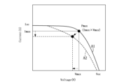
- the output characteristics at room temperature represented by curve A1 shift to curve A2 at temperatures higher than room temperature.
- the higher the temperature the more the maximum operating point Pmax (maximum output power) shifts closer to the origin, resulting in a decrease in output power, so there is a need to promote heat dissipation from the optical power supply converter.
- Patent Document 2 describes a technology in which a semiconductor laser element is sandwiched between a block and a heat sink to promote heat dissipation from the semiconductor laser element, which generates heat when it emits light.
- One electrode of the semiconductor laser element is connected to the block, and the other electrode is connected to the heat sink.
- Patent Document 2 light is emitted from the end face of the semiconductor laser element that is not in contact with the block or heat sink. Therefore, even if the block and heat sink do not transmit light, the block and heat sink can be brought into contact with the front and back sides of the semiconductor laser element, which have a large area, without impeding the emission of light. This makes it easier for heat from the semiconductor laser element to be transferred to the block and heat sink, suppressing the decrease in light emission efficiency and durability caused by heat from the semiconductor laser element.
- a substrate on which the semiconductor light receiving element is mounted is disposed on the front side or the opposite side (back side) of the semiconductor light receiving element of the optical power supply converter where the photodiode is formed, and light is input to the semiconductor light receiving element from the opposite side of the substrate. Therefore, it is difficult to place a member equivalent to a heat sink on the opposite side of the substrate to the semiconductor light receiving element, as this would block the input light.
- the present invention aims to provide an optical power converter that can suppress the temperature rise of the semiconductor light receiving element.
- the optical power supply converter of the invention of claim 1 is an optical power supply converter having a semiconductor light receiving element that photoelectrically converts input light input through an optical fiber cable, and a base for fixing the semiconductor light receiving element, characterized in that the semiconductor light receiving element has a photodiode on a first surface side of a semiconductor substrate that is transparent to the input light, and the first surface side is fixed to the base, and a heat transfer member that is transparent to the input light and is in close contact with a second surface side facing the first surface of the semiconductor substrate is fixed to the base, the input light is configured to pass through the heat transfer member and be incident on the semiconductor light receiving element, and a portion of the heat of the semiconductor light receiving element is configured to be transferred to the base via the heat transfer member.
- the input light input through the optical fiber cable passes through the heat transfer member attached to the semiconductor light receiving element and enters the semiconductor light receiving element, and a portion of the heat of the semiconductor light receiving element is transferred to the base via the heat transfer member. Therefore, the heat of the semiconductor light receiving element is transferred to the base not only from the first surface side on which the photodiode is formed, but also from the second surface side via the heat transfer member, so that the heat dissipation of the semiconductor light receiving element 10 can be promoted to reduce the temperature rise, and the output reduction of the optical power supply converter can be suppressed.
- the optical power supply converter of the invention of claim 2 is the invention of claim 1, characterized in that the heat transfer member is integrally formed with legs that extend toward the base and are fixed to the base. According to the above configuration, since the legs are integrally formed with the heat transfer member, the interface between the legs and the base is generally the only interface at which heat transfer is difficult, making it easier to transfer heat to the base.
- the optical power supply converter of the invention of claim 3 is the invention of claim 1, characterized in that a support portion extending toward the heat transfer member and to which the heat transfer member is fixed is integrally formed on the base. According to the above configuration, the support part to which the heat transfer member is fixed is formed integrally with the base, so that the only interface that generally has difficulty in transferring heat is the interface between the heat transfer member and the support part, making it easier to transfer heat to the base.
- the optical power supply converter of the present invention is the optical power supply converter of the first aspect, characterized in that the heat transfer member is fixed to the base via a spacer member. According to the above configuration, by fixing the heat transfer member to the base via the spacer member, when the spacer member is formed from a material with excellent thermal conductivity, it is possible to easily transfer heat from the heat transfer member to the base, and it also becomes easier to form the heat transfer member and the base.
- the optical power supply converter of the invention of claim 5 is characterized in that, in the invention of claim 1, the photodiode is formed by connecting in series a plurality of equal segments divided by grooves extending radially from a center through which the optical axis of the input light passes in a direction perpendicular to the optical axis, and the heat transfer member has a conical concave surface formed so that its axis of symmetry coincides with the optical axis in an area where the input light is irradiated on the opposite side to a contact surface that is in close contact with the second surface side of the semiconductor substrate.
- the photodiode in order to increase the output voltage, is formed by connecting a plurality of segments, each of which is equally divided by a plurality of grooves extending radially from the center, in series.
- the irradiation area of the input light from the optical fiber cable is circular, and the light intensity distribution is rotationally symmetrical with respect to the optical axis and the light intensity decreases as it moves away from the optical axis. Therefore, in order to make the light evenly incident on the plurality of segments, the input light is input so that the optical axis passes through the center of the photodiode.
- the heat transfer member Since the heat transfer member has a conical concave surface formed in the area where the input light is irradiated, the circular irradiation area of the input light incident on this concave surface is converted into an annular shape and incident on the photodiode. Therefore, the input light is effectively utilized by making the part of the input light near the optical axis, which has a high light intensity, incident on the photodiode while avoiding the vicinity of the center of the photodiode where the grooves that cannot be photoelectrically converted are concentrated. This also makes it possible to promote heat dissipation from the semiconductor light receiving element.
- the optical power converter of the present invention can suppress the temperature rise of the semiconductor light receiving element, and can suppress the decrease in output due to the temperature rise.
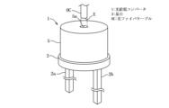
- FIG. 1 is an external view of an optical power supply converter according to an embodiment of the present invention.
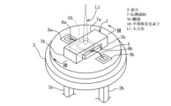
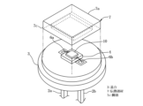
- FIG. 2 is a perspective view of the optical power supply converter with the cover removed.
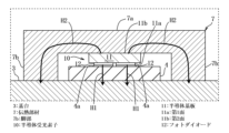
- 3 is a cross-sectional view of a main part of the optical power supply converter shown in FIG. 2 taken along line III-III.
- FIG. 11 is an exploded perspective view showing another example of the heat transfer member. 13 is a graph showing the effect of a heat transfer member.
- FIG. 4 is a cross-sectional view showing an example of a heat transfer member and a base. 7 is a graph showing the effect of the heat transfer member of FIG. 6 .
- 11 is a cross-sectional view showing another example of the heat transfer member and the base.
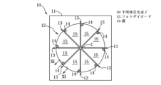
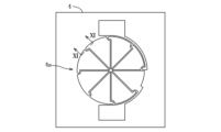
- FIG. 2 is a plan view showing a first surface side of a semiconductor substrate of the semiconductor light receiving element; 10 is a plan view showing a wiring portion of a substrate on which the semiconductor light receiving element of FIG. 9 is mounted.
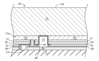
- 11 is a cross-sectional view of a main part of the semiconductor light receiving element of FIG. 9 mounted on the substrate of FIG. 10 taken along the line XI-XI.
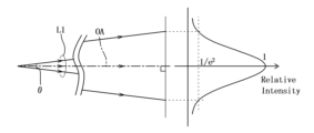
- FIG. 4 is an explanatory diagram of a light intensity distribution of input light.
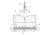
- FIG. 2 is an explanatory diagram of a heat transfer member having a conical concave surface.
- 10 is an explanatory diagram of input light entering a semiconductor light receiving element through a conical concave surface of a heat transfer member; 1 is a diagram illustrating a decrease in output characteristics due to a rise in temperature of a photovoltaic power supply converter.
- the optical power supply converter 1 has a pair of output terminals 2a, 2b for converting light (input light L1) input via, for example, a single-mode optical fiber cable OC into a current and supplying power to the outside.
- a substrate 4 is fixed to a base 3 (stem) equipped with the pair of output terminals 2a, 2b, on which a semiconductor light receiving element 10 is mounted for generating a current from the input light L1 by photoelectric conversion.
- a cover 5 is fixed to the base 3 to protect and block light from the semiconductor light receiving element 10.
- the input light L1 which is input to the semiconductor light receiving element 10 from the opening 5a provided in the cover 5 via the optical fiber cable OC, is often infrared light with a wavelength in the range of, for example, 1 to 1.6 ⁇ m. After being emitted from the output end E of the optical fiber cable OC, this input light L1 is a conical beam whose irradiation range increases as it travels.
- the semiconductor light receiving element 10 is a back-illuminated type light receiving element, and as shown in Figs. 2 and 3, a photodiode 12 is formed on the first surface 11a (front side) of a semiconductor substrate 11 that is transparent to the input light L1, and this first surface 11a side is fixed to the substrate 4.
- the substrate 4 has a wiring portion 4a for extracting the photocurrent generated by the semiconductor light receiving element 10, and the wiring portion 4a is connected to the output terminal portions 2a and 2b by, for example, conductive wires 6a and 6b, respectively.
- the semiconductor light receiving element 10 has the first surface 11a side facing the base 3, and the first surface 11a side is fixed to the base 3 via the substrate 4.
- the input light L1 is input from the second surface 11b side (back side) facing the first surface 11a of the semiconductor substrate 11.
- the substrate 4 is preferably a ceramic substrate, which has better thermal conductivity than an epoxy substrate.
- the output terminals 2a and 2b are fixed to the base 3, which is made of Kovar, a material that is mainly composed of iron and has a low thermal expansion coefficient, via insulating members 3a and 3b.
- a heat transfer member 7 is also fixed to the base 3, which is in close contact with the second surface 11b of the semiconductor light receiving element 10, so as to cover the semiconductor light receiving element 10 and the substrate 4.
- the heat transfer member 7 has a main body 7a formed in a rectangular plate shape and two legs 7b extending from both longitudinal ends of the main body 7a toward the base 3.
- the main body 7a is a plate made of, for example, silicon (Si) that is transparent to the input light L1 and has excellent thermal conductivity.
- the thermal conductivity of silicon is lower than that of, for example, gold, copper, aluminum, etc., which are used as wiring materials, but is higher than that of, for example, glass, which is transparent to the input light L1.
- the two legs 7b are formed integrally with the main body 7a, making it easy for heat to be transferred from the main body 7a to the legs 7b.
- the two legs 7b are fixed to the base 3 by, for example, a thermally conductive paste as an adhesive.
- the semiconductor light receiving element 10 and the substrate 4 sandwiched between the heat transfer member 7 and the base 3 are accommodated between the two legs 7b.
- the main body 7a of the heat transfer member 7 has a portion (contact surface) that is brought into close contact with the second surface 11b of the semiconductor substrate 11 of the semiconductor light receiving element 10, which is polished flat, for example.
- the second surface 11b of the semiconductor substrate 11 of the semiconductor light receiving element 10 that is brought into close contact with the heat transfer member 7 is also polished flat, for example.
- the input light L1 passes through the heat transfer member 7 and the semiconductor substrate 11 of the semiconductor light receiving element 10 and enters the photodiode 12. A part of this input light L1 is converted into a current by photoelectric conversion and output, and the rest becomes heat, which increases the temperature of the semiconductor light receiving element 10. Most of the heat from the semiconductor light receiving element 10 is transferred to the base 3.
- the heat transfer path is a path that transfers to the base 3 via the substrate 4 on the first surface 11a side as shown by arrow H1, and a path that transfers to the base 3 via the heat transfer member 7 on the second surface 11b side as shown by arrow H2.
- the only part of the path indicated by arrow H2 where heat transfer is difficult is the interface between the leg 7b of the heat transfer member 7 and the base 3, but the heat transfer is improved by, for example, a thermal conductive paste.
- the heat transferred to the base 3 is dissipated from the base 3 to the outside (air, etc.), and is also dissipated to the outside from the cover 5 fixed to the base 3. Heat is transferred to the base 3 from the first surface 11a and the second surface 11b, which have larger areas of the semiconductor light receiving element 10, promoting heat dissipation and minimizing the temperature rise of the semiconductor light receiving element 10.
- the heat transfer member 7 may be formed integrally with a rectangular flat body 7a that is in close contact with the semiconductor light receiving element 10 and legs 7c that run along the outer periphery of the body 7a. This increases the contact area between the heat transfer member 7 and the base 3, making it easier to transfer heat from the semiconductor light receiving element 10 to the base 3 via the heat transfer member 7.
- the inside of the legs 7c houses the substrate 4 on which the semiconductor light receiving element 10 is mounted, including the portion that electrically connects the output terminals 2a, 2b to the substrate 4.
- the heat transfer member 7 may have multiple legs that are formed integrally with the rectangular flat body 7a so as to run along the outer periphery of the body 7a.
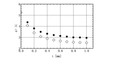
- the temperature of the base 3 is maintained at a constant temperature.
- ⁇ is the type having two legs 7b in Figure 2
- ⁇ is the type having the leg 7c in Figure 4, where the body 7a of the heat transfer member 7 is the same in size, and the thickness of the leg 7b is the same as the thickness of the leg 7c.
- the thickness of the leg refers to the length from the side of the leg facing the semiconductor light receiving element 10 (inside) to the opposite side (outside) in the direction away from the semiconductor light receiving element 10.
- the height of the legs 7b and 7c which corresponds to the total thickness of the semiconductor light receiving element 10 and the substrate 4, is, for example, 0.8 mm.
- the contact area of the leg 7c in FIG. 4 with the base 3 is approximately twice the contact area of the two legs 7b in FIG. 2 with the base 3.
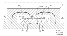
- the heat transfer member 7 is formed in a rectangular plate shape, and the two support parts 3c on which both ends of the heat transfer member 7 in close contact with the semiconductor light receiving element 10 are placed and fixed may be formed integrally with the base 3 so as to protrude from the base 3 toward the heat transfer member 7.
- the heat of the semiconductor light receiving element 10 is transferred to the base 3 via the substrate 4 on the first surface 11a side as shown by arrow H1, and is also transferred to the base 3 via the heat transfer member 7 on the second surface 11b side that is in close contact with the semiconductor light receiving element 10 and the two support parts 3c as shown by arrow H3.
- the only place where heat transfer is difficult in the path of arrow H3 is the interface between the heat transfer member 7 and the support parts 3c, but the heat transfer is improved by, for example, a thermally conductive paste that fixes the heat transfer member 7 to the support parts 3c.
- Heat can be transferred to the base 3 from the first surface 11a and second surface 11b, which have larger areas of the semiconductor light receiving element 10, promoting heat dissipation and minimizing temperature rise.
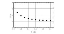
- Figure 7 shows the results of a simulation showing the relationship between the thickness t of the heat transfer member 7 and the temperature rise ⁇ T of the semiconductor light receiving element 10 when 1 W of input light L1 is input to the optical power supply converter 1 having the heat transfer member 7 and base 3 of Figure 6.
- the size of the support 3c is equal to the leg 7b of Figure 2. In this case as well, it can be seen that up to a thickness t of about 0.8 mm of the main body 7a, the thicker the heat transfer member 7 is, the smaller the temperature rise ⁇ T of the semiconductor light receiving element 10 becomes, and the easier it is for the heat of the semiconductor light receiving element 10 to be transferred to the base 3 via the heat transfer member 7.
- the support protruding from the base 3 so as to follow the outer periphery of the heat transfer member 7 formed in a rectangular flat plate shape may be formed integrally with the base 3.
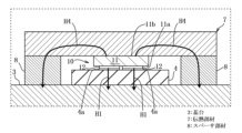
- metal spacer members 8 made of, for example, aluminum or copper, which have better thermal conductivity than the heat transfer member 7, may be disposed on both ends of the heat transfer member 7 formed in a rectangular plate shape, or along the outer periphery of the heat transfer member 7, and the heat transfer member 7 in close contact with the semiconductor light receiving element 10 may be fixed to the base 3 via the spacer members 8.
- the heat of the semiconductor light receiving element 10 is transferred to the base 3 via the substrate 4 on the first surface 11a side as shown by arrow H1, and is transferred to the base 3 via the heat transfer member 7 and spacer member 8 on the second surface 11b side as shown by arrow H4.
- the path of arrow H4 includes the interface between the spacer member 8 and the heat transfer member 7 and the interface between the spacer member 8 and the base 3, but the heat transfer is improved by, for example, a thermally conductive paste, and the heat is transferred from the heat transfer member 7 to the base 3 via the spacer member 8, which has high thermal conductivity. Therefore, heat can be transferred to the base 3 from the first surface 11a and second surface 11b, which have larger areas of the semiconductor light receiving element 10, promoting heat dissipation, minimizing temperature rise, and facilitating the formation of the heat transfer member 7 and base 3.
- the photodiode 12 of the semiconductor light receiving element 10 has a plurality of segments equally divided in the circumferential direction by a plurality of grooves 13 extending radially from the center C of the photodiode 12, as shown in Fig. 9.
- the photodiode 12 is equally divided into eight segments, but the number of divisions is appropriately set according to the required voltage.
- Each of the plurality of segments has a pair of electrodes, and the electrode covering most of the surface of each segment is the second electrode 15, and the other electrode is the first electrode 14.
- a wiring section 4a is formed on the substrate 4 on which the semiconductor light receiving element 10 is mounted.
- the wiring section 4a is formed to correspond to the second electrode 15 of each segment and has a wiring pattern that extends to connect to the first electrode 14 of the adjacent segment, and has wiring patterns for connecting the conductive wires 6a, 6b at both ends of the series connection.
- the multiple first and second electrodes 14, 15 of the semiconductor light receiving element 10 are aligned with the corresponding wiring portion 4a of the substrate 4 and connected, for example, by a lead-free solder paste. This fixes the semiconductor light receiving element 10 to the substrate 4 and forms a photodiode 12 in which multiple segments are connected in series.
- Figure 11 is a cross-sectional view of a main part of this series-connected photodiode 12, and is a cross-sectional view corresponding to the XI-XI line in Figures 9 and 10.
- the multiple segments constituting the photodiode 12 are formed on the first surface 11a side of the semiconductor substrate 11, with a circular PIN photodiode formed by stacking a first semiconductor layer 16, a light absorbing layer 17, and a second semiconductor layer 18, and divided equally in the circumferential direction by multiple grooves 13.
- An insulating layer 19 is formed to cover the inside of the grooves 13 and the second semiconductor layer 18, and a second electrode 15 connected to the second semiconductor layer 18 through an opening formed in the insulating layer 19 is formed so as to cover most of the second semiconductor layer 18.
- the first electrode 14 is connected to the first semiconductor layer 16 through a connection hole that penetrates the second semiconductor layer 18 and the light absorbing layer 17.
- An insulating layer 19 is also formed on the inner wall of the connection hole.
- the semiconductor substrate 11 is, for example, a semi-insulating InP substrate, and the first semiconductor layer 16 is, for example, an n-InP layer.
- the light absorbing layer 17 is, for example, an InGaAs layer
- the second semiconductor layer 18 is, for example, a p-InP layer
- the insulating layer 19 is, for example, a SiO2 layer.
- the first and second electrodes 14, 15 are formed of a metal containing, for example, gold as a main component.
- the wiring portion 4a of the substrate 4 is formed of a metal containing, for example, gold or copper as a main component.
- the first and second electrodes 14, 15 and the corresponding wiring portion 4a are connected by solder paste 20.
- the optical fiber cable OC is fixed so that the optical axis OA of the input light L1 is perpendicular to the photodiode 12 and passes through the center C of the photodiode 12.
- the photodiode 12 which has multiple segments connected in series and equally spaced circumferentially, generates heat in response to the input light L1, causing the temperature of the semiconductor light receiving element 10 to rise.
- a heat transfer member 7 is provided in close contact with the semiconductor light receiving element 10.
- the input light L1 input through the optical fiber cable OC spreads out in a cone shape.
- the light intensity distribution of this input light L1 decreases the further away from the optical axis OA of the input light L1, and becomes a Gaussian distribution that is rotationally symmetrical about the optical axis OA.
- the photodiode 12 has multiple grooves 13 that extend radially from its center C in a direction perpendicular to the optical axis OA, and since photoelectric conversion is not possible in these grooves 13, the areas of high light intensity near the optical axis OA cannot be used near the center C where the multiple grooves 13 are concentrated.
- a conical concave surface 7d is formed in the area of the heat transfer member 7 where the input light L1 is irradiated.
- This concave surface 7d is formed by conically recessing the surface of the rectangular, flat body portion 7a of the heat transfer member 7 opposite the surface that is brought into close contact with the semiconductor light receiving element 10.
- the conical concave surface 7d may be formed by a known etching technique, or the conical concave surface 7d may be formed by polishing.
- the input light L1 spreads away from the optical axis OA by the conical concave surface 7d, and the circular irradiation area becomes annular. Then, the light with the annular irradiation area is incident on the photodiode 12.
- the heat transfer member 7 having a conical concave surface 7d prevents the input light L1 from entering near the center C of the photodiode 12 where the multiple radial grooves 13 gather, allowing the input light L1 to be used effectively.
- the heat of the semiconductor light receiving element 10 is transferred to the base 3 not only through the substrate 4 but also through the heat transfer member 7, promoting heat dissipation from the semiconductor light receiving element 10 and suppressing a rise in temperature of the semiconductor light receiving element 10.
- the conical concave surface 7d can also be formed on the heat transfer member 7 of the type shown in FIG. 4, FIG. 6, or FIG. 8.
- curve A1 shows the output characteristics of the optical power converter at a certain temperature (e.g. room temperature), and curve A2 shows the output characteristics when the temperature rises.
- An increase in temperature causes the maximum output power Pmax to shift closer to the origin, i.e. the maximum output power Pmax decreases.
- the optical power converter 1 equipped with the heat transfer member 7 can reduce the temperature rise by promoting heat dissipation by transferring some of the heat from the semiconductor light receiving element 10 to the base 3 via the heat transfer member 7, thereby reducing this decrease in output.
- the input light L1 input to the optical power supply converter 1 via the optical fiber cable OC passes through the heat transfer member 7 that is in close contact with the semiconductor light receiving element 10 and enters the semiconductor light receiving element 10, and a part of the heat of the semiconductor light receiving element 10 is transferred to the base 3 via the heat transfer member 7. Therefore, the heat of the semiconductor light receiving element 10 is transferred to the base 3 not only from the first surface 11a side on which the photodiode 12 is formed, but also from the second surface 11b side to the base 3 via the heat transfer member 7. Therefore, it is possible to promote heat dissipation from the semiconductor light receiving element 10, reduce a temperature rise, and suppress a decrease in the output of the optical power supply converter 1.
- the only interface where heat transfer is generally difficult is the interface between the legs 7b and the base 3, making it easier to transfer heat to the base 3.
- the support 3c to which the heat transfer member 7 is fixed is formed integrally with the base 3, the only interface where heat transfer is difficult is the interface between the heat transfer member 7 and the support 3c, making it easier to transfer heat to the base 3.
- the heat transfer member 7 is fixed to the base 3 via a spacer member 8 made of a material with excellent thermal conductivity, it is easier to transfer heat to the base 3 and it becomes easier to form the heat transfer member 7 and the base 3.
- the photodiode 12 is formed by connecting multiple segments in series, each segment being equally divided by multiple grooves 13 extending radially from its center C.
- the irradiation area of the input light L1 from the optical fiber cable OC is circular, and its light intensity distribution is rotationally symmetrical with respect to the optical axis OA, with the light intensity decreasing the farther away from the optical axis OA. Therefore, in order to make the input light L1 evenly incident on the multiple segments, the input light L1 is input so that its optical axis OA passes through the center C of the photodiode 12.
- the part of the input light L1 with high light intensity near the optical axis OA is not photoelectrically converted, resulting in a large amount of waste.
- a conical concave surface 7d is formed in the area of the heat transfer member 7 where the input light L1 is irradiated, the circular irradiation area of the input light L1 incident on this concave surface 7d is converted into an annular shape and incident on the photodiode 12. Therefore, the part of the input light L1 with high light intensity is made incident on the photodiode 12, avoiding the vicinity of the center C of the photodiode 12 where the grooves 13 are concentrated, and the input light L1 can be used effectively.
- the substrate 4 may be a silicon substrate having an insulating layer and a wiring portion 4a on the insulating layer.
- the wiring portion 4a of the substrate 4 may be formed on the insulating layer of the base 3, and the substrate 4 may be omitted and the semiconductor light receiving element 10 may be fixed to the base 3 to promote heat dissipation.
- a person skilled in the art may implement the above embodiment in various modified forms without departing from the spirit of the present invention, and the present invention also includes such modified forms.
Landscapes
- Light Receiving Elements (AREA)
Priority Applications (2)
| Application Number | Priority Date | Filing Date | Title |
|---|---|---|---|
| JP2024554013A JP7755757B2 (ja) | 2022-11-02 | 2022-11-02 | 光給電コンバータ |
| PCT/JP2022/041024 WO2024095405A1 (ja) | 2022-11-02 | 2022-11-02 | 光給電コンバータ |
Applications Claiming Priority (1)
| Application Number | Priority Date | Filing Date | Title |
|---|---|---|---|
| PCT/JP2022/041024 WO2024095405A1 (ja) | 2022-11-02 | 2022-11-02 | 光給電コンバータ |
Publications (1)
| Publication Number | Publication Date |
|---|---|
| WO2024095405A1 true WO2024095405A1 (ja) | 2024-05-10 |
Family
ID=90929960
Family Applications (1)
| Application Number | Title | Priority Date | Filing Date |
|---|---|---|---|
| PCT/JP2022/041024 Ceased WO2024095405A1 (ja) | 2022-11-02 | 2022-11-02 | 光給電コンバータ |
Country Status (2)
| Country | Link |
|---|---|
| JP (1) | JP7755757B2 (cg-RX-API-DMAC7.html) |
| WO (1) | WO2024095405A1 (cg-RX-API-DMAC7.html) |
Citations (6)
| Publication number | Priority date | Publication date | Assignee | Title |
|---|---|---|---|---|
| JP2006295222A (ja) * | 2006-07-20 | 2006-10-26 | Sumitomo Electric Ind Ltd | 半導体受光素子モジュール |
| JP2008304611A (ja) * | 2007-06-06 | 2008-12-18 | Fujikura Ltd | 光送受信装置 |
| JP2010114235A (ja) * | 2008-11-06 | 2010-05-20 | Nec Corp | 光電変換素子、光給電装置、及び光電変換素子の製造方法 |
| US20110108081A1 (en) * | 2006-12-20 | 2011-05-12 | Jds Uniphase Corporation | Photovoltaic Power Converter |
| JP6795870B1 (ja) * | 2020-07-06 | 2020-12-02 | 株式会社京都セミコンダクター | 光給電コンバータ |
| JP6836300B1 (ja) * | 2020-09-10 | 2021-02-24 | 株式会社京都セミコンダクター | 面入射型半導体受光素子 |
Family Cites Families (3)
| Publication number | Priority date | Publication date | Assignee | Title |
|---|---|---|---|---|
| JP2006029522A (ja) * | 2004-07-20 | 2006-02-02 | Ntn Corp | 円すいころ軸受 |
| JP4768433B2 (ja) * | 2005-12-22 | 2011-09-07 | シャープ株式会社 | 光半導体装置およびそれを備えた電子機器 |
| JP6650075B2 (ja) * | 2018-02-01 | 2020-02-19 | 株式会社京都セミコンダクター | 半導体受光素子 |
-
2022
- 2022-11-02 WO PCT/JP2022/041024 patent/WO2024095405A1/ja not_active Ceased
- 2022-11-02 JP JP2024554013A patent/JP7755757B2/ja active Active
Patent Citations (6)
| Publication number | Priority date | Publication date | Assignee | Title |
|---|---|---|---|---|
| JP2006295222A (ja) * | 2006-07-20 | 2006-10-26 | Sumitomo Electric Ind Ltd | 半導体受光素子モジュール |
| US20110108081A1 (en) * | 2006-12-20 | 2011-05-12 | Jds Uniphase Corporation | Photovoltaic Power Converter |
| JP2008304611A (ja) * | 2007-06-06 | 2008-12-18 | Fujikura Ltd | 光送受信装置 |
| JP2010114235A (ja) * | 2008-11-06 | 2010-05-20 | Nec Corp | 光電変換素子、光給電装置、及び光電変換素子の製造方法 |
| JP6795870B1 (ja) * | 2020-07-06 | 2020-12-02 | 株式会社京都セミコンダクター | 光給電コンバータ |
| JP6836300B1 (ja) * | 2020-09-10 | 2021-02-24 | 株式会社京都セミコンダクター | 面入射型半導体受光素子 |
Also Published As
| Publication number | Publication date |
|---|---|
| JP7755757B2 (ja) | 2025-10-16 |
| JPWO2024095405A1 (cg-RX-API-DMAC7.html) | 2024-05-10 |
Similar Documents
| Publication | Publication Date | Title |
|---|---|---|
| CN110388576B (zh) | 一种光模块 | |
| CN111352192B (zh) | 一种光模块 | |
| US12174438B2 (en) | Optical module with structured protective cover | |
| US4267559A (en) | Low thermal impedance light-emitting diode package | |
| CN103915402B (zh) | 光电模块结构 | |
| US20160226592A1 (en) | Integrated parallel optical transceiver | |
| JP2010041033A (ja) | Ledチップからの光導出を高める改良ボンドパッドのデザイン | |
| CN115144977B (zh) | 一种光模块 | |
| JP2012128387A (ja) | 光導波路デバイスおよびこれを用いた光伝送装置 | |
| JP2018074104A (ja) | 光検出器 | |
| US20190067161A1 (en) | Semiconductor laser module and method for manufacturing the same | |
| JP7755757B2 (ja) | 光給電コンバータ | |
| JP7017829B1 (ja) | 光給電コンバータ | |
| TW201602663A (zh) | 具有散熱結構的主動光學組件 | |
| Peña et al. | One‐watt fiber‐based power‐by‐light system for satellite applications | |
| JP2010161146A (ja) | 光送信モジュール | |
| KR100720789B1 (ko) | 방열구조가 개선된 양방향 광송수신 모듈 | |
| JP2005086094A (ja) | レーザダイオードモジュール | |
| JP2011086737A (ja) | 熱電変換モジュール | |
| CN104718672B (zh) | 光电组件 | |
| JP6972067B2 (ja) | 半導体装置 | |
| US20030107114A1 (en) | Thermal circuitry | |
| JP7246808B1 (ja) | 光給電コンバータ | |
| JP7181462B2 (ja) | 光検出器 | |
| US10748732B2 (en) | Microelectromechanical light emitter component, light emitter component and method for producing a microelectromechanical light emitter component |
Legal Events
| Date | Code | Title | Description |
|---|---|---|---|
| 121 | Ep: the epo has been informed by wipo that ep was designated in this application |
Ref document number: 22964425 Country of ref document: EP Kind code of ref document: A1 |
|
| WWE | Wipo information: entry into national phase |
Ref document number: 2024554013 Country of ref document: JP |
|
| NENP | Non-entry into the national phase |
Ref country code: DE |
|
| 122 | Ep: pct application non-entry in european phase |
Ref document number: 22964425 Country of ref document: EP Kind code of ref document: A1 |