WO2024090248A1 - コネクタシステム及びコネクタ - Google Patents
コネクタシステム及びコネクタ Download PDFInfo
- Publication number
- WO2024090248A1 WO2024090248A1 PCT/JP2023/037226 JP2023037226W WO2024090248A1 WO 2024090248 A1 WO2024090248 A1 WO 2024090248A1 JP 2023037226 W JP2023037226 W JP 2023037226W WO 2024090248 A1 WO2024090248 A1 WO 2024090248A1
- Authority
- WO
- WIPO (PCT)
- Prior art keywords
- mating
- shell
- contact
- insulating housing
- connector
- Prior art date
Links
- 230000013011 mating Effects 0.000 claims abstract description 328
- 239000004020 conductor Substances 0.000 claims description 60
- 230000008054 signal transmission Effects 0.000 description 47
- 238000005476 soldering Methods 0.000 description 20
- 210000000078 claw Anatomy 0.000 description 10
- 239000002184 metal Substances 0.000 description 6
- 238000005452 bending Methods 0.000 description 5
- 239000000463 material Substances 0.000 description 5
- 238000000034 method Methods 0.000 description 5
- 238000004080 punching Methods 0.000 description 5
- 230000015556 catabolic process Effects 0.000 description 4
- 238000006731 degradation reaction Methods 0.000 description 4
- 238000000465 moulding Methods 0.000 description 4
- 239000011347 resin Substances 0.000 description 4
- 229920005989 resin Polymers 0.000 description 4
- 238000013459 approach Methods 0.000 description 1
- 230000005540 biological transmission Effects 0.000 description 1
- 230000000295 complement effect Effects 0.000 description 1
- 238000011109 contamination Methods 0.000 description 1
- 238000006073 displacement reaction Methods 0.000 description 1
- 230000010365 information processing Effects 0.000 description 1
- 238000004382 potting Methods 0.000 description 1
- 238000003825 pressing Methods 0.000 description 1
- 230000001105 regulatory effect Effects 0.000 description 1
- 238000007789 sealing Methods 0.000 description 1
Images


Classifications
-
- H—ELECTRICITY
- H01—ELECTRIC ELEMENTS
- H01R—ELECTRICALLY-CONDUCTIVE CONNECTIONS; STRUCTURAL ASSOCIATIONS OF A PLURALITY OF MUTUALLY-INSULATED ELECTRICAL CONNECTING ELEMENTS; COUPLING DEVICES; CURRENT COLLECTORS
- H01R12/00—Structural associations of a plurality of mutually-insulated electrical connecting elements, specially adapted for printed circuits, e.g. printed circuit boards [PCB], flat or ribbon cables, or like generally planar structures, e.g. terminal strips, terminal blocks; Coupling devices specially adapted for printed circuits, flat or ribbon cables, or like generally planar structures; Terminals specially adapted for contact with, or insertion into, printed circuits, flat or ribbon cables, or like generally planar structures
- H01R12/70—Coupling devices
- H01R12/71—Coupling devices for rigid printing circuits or like structures
- H01R12/75—Coupling devices for rigid printing circuits or like structures connecting to cables except for flat or ribbon cables
-
- H—ELECTRICITY
- H01—ELECTRIC ELEMENTS
- H01R—ELECTRICALLY-CONDUCTIVE CONNECTIONS; STRUCTURAL ASSOCIATIONS OF A PLURALITY OF MUTUALLY-INSULATED ELECTRICAL CONNECTING ELEMENTS; COUPLING DEVICES; CURRENT COLLECTORS
- H01R13/00—Details of coupling devices of the kinds covered by groups H01R12/70 or H01R24/00 - H01R33/00
- H01R13/648—Protective earth or shield arrangements on coupling devices, e.g. anti-static shielding
- H01R13/658—High frequency shielding arrangements, e.g. against EMI [Electro-Magnetic Interference] or EMP [Electro-Magnetic Pulse]
- H01R13/6581—Shield structure
- H01R13/6582—Shield structure with resilient means for engaging mating connector
-
- H—ELECTRICITY
- H01—ELECTRIC ELEMENTS
- H01R—ELECTRICALLY-CONDUCTIVE CONNECTIONS; STRUCTURAL ASSOCIATIONS OF A PLURALITY OF MUTUALLY-INSULATED ELECTRICAL CONNECTING ELEMENTS; COUPLING DEVICES; CURRENT COLLECTORS
- H01R13/00—Details of coupling devices of the kinds covered by groups H01R12/70 or H01R24/00 - H01R33/00
- H01R13/648—Protective earth or shield arrangements on coupling devices, e.g. anti-static shielding
- H01R13/658—High frequency shielding arrangements, e.g. against EMI [Electro-Magnetic Interference] or EMP [Electro-Magnetic Pulse]
- H01R13/6581—Shield structure
- H01R13/6585—Shielding material individually surrounding or interposed between mutually spaced contacts
Definitions
- This disclosure relates to a connector system and a connector.
- Patent Document 1 discloses a receptacle connector that is connected to a plug connector.
- the plug connector has a conductive signal contact member that is connected to the inner conductor of the cable, and a conductive shell portion that surrounds the signal contact member.
- the receptacle connector has a conductive contact member that is connected to the signal contact member of the plug connector, and a conductive shell portion that surrounds the contact member and is connected to the shell portion of the plug connector.
- This disclosure provides a connector system that is effective in achieving both reliable signal transmission and compact size.
- the connector system includes a connector having an insulating housing, conductive contacts held in the insulating housing, and a conductive shell held in the insulating housing so as to be arranged around the contacts; a mating connector having a mating insulating housing that mates with the insulating housing along a mating direction, a conductive mating contact that is held in the mating insulating housing and that comes into contact with the contact when the mating insulating housing is mated with the insulating housing, and a conductive mating shell that is held in the mating insulating housing and that cooperates with the shell to form an enclosure that surrounds the contact and the mating contact around an axis along the mating direction when the mating insulating housing is mated with the insulating housing, and the length of each of the portion where the shell forms the enclosure without overlapping with the mating shell and the portion where the mating shell forms the enclosure without overlapping with the shell in the circumferential direction around the axis is longer than the total
- the connector further has a conductive second contact held in the insulating housing so as to be aligned with the contact along an arrangement direction perpendicular to the mating direction, and a conductive second shell held in the insulating housing so as to be arranged around the second contact
- the mating connector further has a conductive mating second contact held in the mating insulating housing so as to be aligned with the mating contact along the arrangement direction and which comes into contact with the second contact when the mating insulating housing is mated to the insulating housing, and a conductive mating second shell held in the mating insulating housing and which cooperates with the second shell to form a second enclosure surrounding the second contact and the mating second contact around an axis along the mating direction when the mating insulating housing is mated to the insulating housing, and in the circumferential direction around the axis, the respective lengths of the portion where the second shell forms the second enclosure without overlapping with the mating second shell and the portion where the mating second shell forms the second
- the contact and the second contact may be electrically connected to a first signal line and a second signal line in the circuit board, and the mating contact and the mating second contact may be electrically connected to a first signal conductor and a second signal conductor of one or more cables. This is effective in miniaturizing the device in which the circuit board is mounted.
- the insulating housing has a surface facing the circuit board, and the arrangement direction and mating direction may be parallel to the facing surface. This is effective in miniaturizing the connector relative to the circuit board.
- the shell may include a contact portion that contacts the mating shell in a portion where the shell and the mating shell overlap to form an enclosure.
- the contact between the shell and the mating shell can further improve the reliability of signal transmission.
- the enclosure may surround the contact and the mating contact without interruption. Contact between the shell and the mating shell can further improve the reliability of signal transmission.
- the length of the portion of the shell that does not overlap with the mating shell and forms the enclosure, and the length of the portion of the shell that does not overlap with the mating shell and forms the enclosure, may each occupy 1/4 or more of the entire circumference of the enclosure. This is even more effective in reducing the size.
- the portion of the shell that does not overlap with the mating shell and forms the enclosure includes a pair of side portions that face each other in an opposing direction perpendicular to the fitting direction, and a base portion that connects the pair of side portions, and the portion of the shell that does not overlap with the mating shell and forms the enclosure may include a mating base portion that faces the base portion. This is even more effective in reducing size.
- the shell may have a pair of overlapping portions that are connected to a pair of side portions, respectively, and the mating shell may have a pair of mating overlapping portions that face each other in the opposing direction, overlap the pair of overlapping portions from the inside, and are maintained in contact with the shell. This is even more effective in achieving both reliable signal transmission and compact size.
- the shell may overlap with the mating shell along the circumferential direction around the axis. This is even more effective in reducing size.
- the shell may have a wall portion with a slit formed along the mating direction, and the mating shell may have a mating wall portion that intersects with the wall portion and fits into the slit, thereby maintaining contact with the shell along the circumferential direction. This is even more effective in achieving both reliable signal transmission and compact size.
- the mating shell may further have a mating cross wall portion that crosses the mating wall portion, and a mating slit is formed in the mating cross wall portion along the mating direction, and the shell may have a cross wall portion that crosses the mating cross wall portion and fits into the mating slit, thereby being maintained in contact with the mating shell along the circumferential direction. This is further effective in achieving both reliable signal transmission and compact size.
- a connector according to another aspect of the present disclosure is a connector that is connected to a mating connector having a mating insulating housing, a conductive mating contact held in the mating insulating housing, and a conductive mating shell held in the mating insulating housing so as to be arranged around the mating contact, and includes an insulating housing that mates with the mating insulating housing along the mating direction, a conductive contact that is held in the insulating housing and comes into contact with the mating contact when the insulating housing is mated with the mating insulating housing, and a conductive shell that is held in the insulating housing and cooperates with the mating shell to form an enclosure that surrounds the contact and the mating contact around an axis along the mating direction when the insulating housing is mated with the mating insulating housing, and the length of each of the portion where the shell forms the enclosure without overlapping with the mating shell and the portion where the mating shell forms the enclosure without overlapping with the shell in the circumfer
- This disclosure provides a connector system that is effective in achieving both reliable signal transmission and compact size.
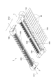
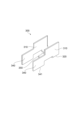
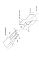
- FIG. 1 is a perspective view illustrating a connector system.
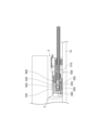
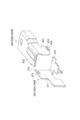
- FIG. 2 is a perspective view of the connector system of FIG. 1 as seen from below.
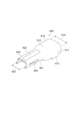
- FIG. 2 is a cross-sectional view taken along line III-III in FIG. 4 is a cross-sectional view showing a state in which the mating connector in FIG. 3 is fitted into the connector.
- 2 is a perspective view of the connector in FIG. 1 as viewed from below.
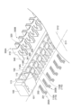
- FIG. 6 is an exploded perspective view of the connector in FIG. 5 .
- FIG. 7 is a partially enlarged view of FIG. 6 .
- FIG. 4 is an enlarged view of the shell of the connector as viewed from above.
- FIG. 4 is an enlarged view of the shell of the connector as viewed from below.
- FIG. 4 is an enlarged view of the shell of the connector as viewed from below.
- FIG. 2 is an exploded perspective view of the mating connector in FIG. 1 .
- FIG. 11 is a partially enlarged view of FIG. 4 is an enlarged view of the mating shell of the mating connector as viewed from above.
- FIG. 4 is an enlarged view of the mating shell of the mating connector as viewed from below.
- FIG. 1 is a perspective view illustrating an example of a combination of a shell and a mating shell.
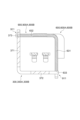
- FIG. FIG. 2 is a cross-sectional view illustrating an example of an enclosure.
- FIG. 13 is a perspective view showing a modified example of the shell and the mating shell.
- FIG. 13 is a perspective view showing a modified example of the enclosure.
- the connector system 1 shown in Fig. 1 and Fig. 2 is used to connect a circuit board 10 (shown in Fig. 3) and a plurality of cables 20 in an application requiring transmission of high-frequency signals with low degradation and a low profile.
- An example of such an application is an information processing system in which signals are transmitted on the circuit board 10 by a plurality of cables 20 instead of printed wiring on the circuit board 10.
- signals can be transmitted with higher signal transmission characteristics than printed wiring.
- the signal transmission characteristics mean less signal degradation in signal transmission, and high signal transmission characteristics mean less signal degradation in signal transmission. Specific examples of signal degradation include noise contamination due to crosstalk and signal attenuation.
- connection points between the circuit board 10 and the multiple cables 20 In order to further improve the signal transmission characteristics of the multiple cables 20, it is necessary to place the connection points between the circuit board 10 and the multiple cables 20 closer to the circuit elements (e.g., a processor) on the circuit board 10. To locate the connection points between the circuit board 10 and the multiple cables 20 near the circuit elements, it is necessary to avoid interference with heat sinks and the like provided on the circuit elements. For this reason, it is necessary to reduce the height of the connector system 1.
- the connector system 1 includes a connector 2 and a connector 3.
- the connector 2 is, for example, a receptacle connector, and is connected to a circuit board 10.
- the connector 3 is, for example, a plug connector, and is connected to a plurality of cables 20.
- the connector 3 can be connected to the connector 2.
- the plurality of cables 20 are electrically connected to the circuit board 10.
- the connectors 2 and 3 are fitted together along a fitting direction D12 parallel to the circuit board 10.
- the connector 3 may be referred to as the "mating connector" for the connector 2, but this does not necessarily mean that only the connector 3 corresponds to the "mating connector", and the connector 2 is the "mating connector" for the connector 3.
- the connector 2 comprises a plurality of contacts 200, a plurality of shells 300, and an insulating housing 100.
- the plurality of contacts 200 are held in the insulating housing 100 so as to be aligned along an arrangement direction D11 that is parallel to the main surface of the circuit board 10 and perpendicular to the mating direction D12.
- Each of the plurality of contacts 200 is electrically connected to the circuit board 10 and contacts a signal contact of the mating connector (connector 3).
- Each of the plurality of shells 300 is held in the insulating housing 100 so as to be arranged around at least one contact 200.
- each of the plurality of shells 300 is held in the insulating housing 100 so as to surround at least one contact 200 around an axis along the mating direction D12.
- the multiple contacts 200 transmit multiple types of signals.
- the multiple shells 300 may be provided for each of the multiple types of signals. In this case, in the area surrounded by each of the multiple shells 300, only one type of signal is transmitted, and other signals are not transmitted.
- each of the multiple contacts 200 may transmit one type of signal based on the ground potential.
- the multiple shells 300 are provided for each of the multiple contacts 200.
- Each of the multiple shells 300 surrounds only one contact 200, and does not surround the other contacts 200.
- the multiple contacts 200 may include multiple pairs of contacts 200 that each transmit multiple types of differential signals. In this case, the multiple shells 300 are provided for each of the multiple pairs of contacts 200. Each of the multiple shells 300 surrounds only one pair of contacts 200, and does not surround the other contacts 200.
- the insulating housing 100 holds the multiple contacts 200 and the multiple shells 300 together.
- the insulating housing 100 keeps the multiple contacts 200 insulated from each other, keeps the multiple shells 300 insulated from each other, and keeps the multiple contacts 200 and the multiple shells 300 insulated from each other.
- the connector 3 comprises a base unit 500 and a number of shells 600.
- the base unit 500 has a connector base 510, a number of insulating housings 520, and a number of conductive contacts 530.
- the connector base 510 extends along the arrangement direction D11 (D21).
- the multiple insulating housings 520 are aligned along the arrangement direction D11, and each protrude in the same direction from the connector base 510 along the mating direction D12 (D22).
- the multiple contacts 530 are held in the multiple insulating housings 520 so as to be aligned along the arrangement direction D11.
- Each of the multiple contacts 530 is electrically connected to one of the multiple cables 20 and contacts the contacts 200 of the mating connector (connector 2).
- Each of the multiple insulating housings 520 holds at least one contact 530.
- the multiple contacts 530 may transmit the multiple types of signals described above, and multiple insulating housings 520 may be provided for each of the multiple types of signals. In this case, only one type of signal is transmitted in the multiple insulating housings 520, and no other signals are transmitted. As an example, each of the multiple contacts 530 may transmit one type of signal based on the ground potential. In this case, multiple insulating housings 520 are provided for each of the multiple contacts 530. Each of the multiple insulating housings 520 holds only one contact 530 and does not hold any other contacts 530.
- the multiple contacts 530 may include multiple pairs of contacts 530 that each transmit multiple types of differential signals. In this case, multiple insulating housings 520 are provided for each of the multiple pairs of contacts 530. Each of the multiple insulating housings 520 holds only a pair of contacts 530 and does not hold any other contacts 530.
- the multiple shells 600 correspond to the multiple insulating housings 520, respectively. Each of the multiple shells 600 surrounds the corresponding insulating housing 520 around an axis along the mating direction D12 (D22).
- the insulating housings 520 correspond to the shells 300, respectively. As shown in Figures 3 and 4, each of the insulating housings 520 is inserted into the corresponding shell 300 along the mating direction D12. Each of the shells 600 is mated with the corresponding shell 300 along the mating direction D12. Each of the contacts 530 contacts the corresponding contact 200 in the corresponding shell 300. This electrically connects the cables 20 to the circuit board 10.
- the relationship between the contacts 200 and the shells 300 can be individually optimized. Furthermore, the shells 300 surround the contacts 200 around an axis along the mating direction D12 parallel to the circuit board 10. This restricts the mating direction of the connector 3 to the connector 2 to a direction parallel to the circuit board 10. This makes it possible to reduce the height of the connection formed by the connectors 2 and 3 (reducing the height relative to the surface of the circuit board 10). This is therefore effective in achieving both improved signal transmission characteristics and a reduced height.
- Each of the multiple shells 300 may complement the surrounding of the insulating housing 520 by the corresponding shell 600.
- the shell 300 may surround the periphery of the insulating housing 520 that is not surrounded by the shell 600. This reduces the overlap between the shells 600 and 300, making it possible to further reduce the height.
- connector 2 and connector 3 are illustrated in more detail below.
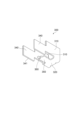
- FIG. 5 is a perspective view of the connector 2 as seen from below
- Fig. 6 is an exploded perspective view of the connector 2 in Fig. 5.
- the connector 2 has an insulating housing 100, a plurality of conductive contacts 200, and a plurality of conductive shells 300.
- the insulating housing 100 has an opposing surface 101, a recessed surface 102, and multiple protrusions 110.
- the opposing surface 101 faces the circuit board 10.
- the arrangement direction D11 and the mating direction D12 are parallel to the opposing surface 101.
- the recessed surface 102 faces the circuit board 10 at a position away from the circuit board 10 when the opposing surface 101 faces the circuit board 10.
- the multiple protrusions 110 are aligned along the arrangement direction D11 parallel to the opposing surface 101, and each protrudes from the recessed surface 102.
- the multiple protrusions 110 correspond to the multiple shells 300, respectively.
- Each of the multiple shells 300 is held by the corresponding protrusion 110.
- At least one contact 200 surrounded by each of the multiple shells 300 is also held by the protrusion 110.
- a pair of contacts 200 surrounded by each of the multiple shells 300 are held by the protrusion 110 so as to be aligned along the arrangement direction D11.
- the insulating housing 100 is formed by molding a resin material, etc.
- a single convex portion 110, the corresponding shell 300, and a pair of contacts 200 constitute one set of signal transmission parts TP1.
- the connector 2 includes multiple sets of signal transmission parts TP1 corresponding to the multiple convex portions 110, respectively.
- the multiple sets of signal transmission parts TP1 are aligned along the arrangement direction D11, and each transmit the multiple types of signals described above. Below, a more detailed configuration example is provided for the first and second sets of signal transmission parts TP1 from the left side of the illustration, which are representative of the multiple sets of signal transmission parts TP1.
- the multiple sets of signal transmission parts TP1 have the same configuration, but for ease of explanation, the convex part 110, contact 200, and shell 300 belonging to the first signal transmission part TP1 from the left in the figure are distinguished from one another as the first convex part 110A, first contact 200A, and first shell 300A, and the convex part 110, contact 200, and shell 300 belonging to the second signal transmission part TP1 from the left in the figure are distinguished from one another as the second convex part 110B, second contact 200B, and second shell 300B.
- the first contact 200A and the second contact 200B are held in the insulating housing 100 so as to be aligned along the arrangement direction D11.
- the first contact 200A and the second contact 200B are electrically connected to a pair of signal lines 13 on the circuit board 10.
- the "pair of signal lines 13" to which the first contact 200A and the second contact 200B are respectively connected transmit different signals.
- the first convex portion 110A includes a pair of first contacts 200A and the second convex portion 110B includes a pair of second contacts 200B
- the pair of first contacts 200A are held in the first convex portion 110A so as to be aligned along the arrangement direction D11
- the pair of second contacts 200B are held in the second convex portion 110B so as to be aligned along the arrangement direction D11
- the pair of first contacts 200A and the pair of second contacts 200B are aligned along the arrangement direction D11 in accordance with the arrangement of the first convex portion 110A and the second convex portion 110B.
- the pair of first contacts 200A are electrically connected to a pair of signal lines 13 that transmit a first differential signal on the circuit board 10.
- the pair of second contacts 200B are electrically connected to a pair of signal lines 13 that transmit a second differential signal different from the first differential signal on the circuit board 10.
- Each of the pair of first contacts 200A has a connection portion 201 (first connection portion) and a contact portion 202 (first contact portion).
- the connection portion 201 is electrically connected to the circuit board 10.
- the connection portion 201 is connected to a conductive signal terminal formed on the circuit board 10 by soldering or the like.
- the contact portion 202 protrudes from the connection portion 201 along a mating direction D12 that is parallel to the opposing surface 101 and perpendicular to the arrangement direction D11.
- the protruding direction of the contact portion 202 relative to the connection portion 201 will be referred to as the "forward direction” and the opposite direction will be referred to as the "rearward direction”.
- the first contact 200A is bent in a crank shape between the connection portion 201 and the contact portion 202 so that the contact portion 202 is located away from the circuit board 10.
- the first contact 200A is formed, for example, by punching and bending a thin metal plate material.
- Each of the pair of second contacts 200B is configured similarly to the first contact 200A and has a connection portion 201 (second connection portion) and a contact portion 202 (second connection portion).
- the connection portion 201 of the second contact 200B is connected by soldering or the like to a conductive signal terminal formed on the circuit board 10 separately from the signal terminal to which the connection portion 201 of the first contact 200A is connected.
- the first shell 300A is held in the insulating housing 100 so as to be arranged around the pair of first contacts 200A.
- the first shell 300A is held in the insulating housing 100 so as to surround the pair of first contacts 200A around an axis along the mating direction D12, and is electrically connected to the circuit board 10 with the opposing surface 101 facing the circuit board 10.
- the first shell 300A may partially surround the pair of first contacts 200A.
- the first shell 300A surrounds at least the contact portions 202 of the pair of first contacts 200A.
- the first shell 300A no signals are transmitted other than the one type of signal transmitted by at least one first contact 200A.
- the one type of signal is the only signal transmitted in the first shell 300A.
- only the first differential signal is transmitted, and no other signals are transmitted.
- the first shell 300A surrounds only the pair of first contacts 200A, and does not surround the other contacts 200.
- the first shell 300A may surround the pair of first contacts 200A in a circular shape, or may surround the pair of first contacts 200A in a polygonal shape. As an example, the first shell 300A may surround the first contacts 200A in a rectangular shape.
- the first shell 300A has a pair of side wall portions 310 (first side wall portions) and a base portion 320 (first base portion) (see FIG. 8).
- the pair of side wall portions 310 face each other along the arrangement direction D11.
- the contact portion 202 of the pair of first contacts 200A is located between the pair of side wall portions 310.
- the base portion 320 extends parallel to the facing surface 101 and connects the pair of side wall portions 310. With the facing surface 101 facing the circuit board 10, the base portion 320 may be located between the contact portion 202 and the circuit board 10.
- a receiving space IS (first receiving space) is formed between a pair of side wall portions 310.
- a mating first housing (one of the multiple insulating housings 520) of a mating connector (connector 3) is inserted into the receiving space IS along the mating direction D12.
- the mating shell (shell 600A) of the mating connector is mated with the first shell 300A, and the mating signal contact (contact 530A) held in the mating first housing contacts the contact portion 202 of the first contact 200A (see FIG. 4).
- the pair of contacts 530A each contacts the contact portion 202 of the pair of first contacts 200A.
- the first shell 300A may further have a pair of protruding portions 340 (first protruding portions) that protrude rearward from the pair of side wall portions 310.
- the connection portions 201 of the pair of first contacts 200A are located between the pair of protruding portions 340.
- the first shell 300A may further have a pair of shell connection parts 341 (first shell connection parts) formed on the pair of protrusions 340, respectively, so as to be electrically connected to the circuit board 10 when the opposing surface 101 faces the circuit board 10.
- each of the pair of shell connection parts 341 is formed on the lower edge of the corresponding protrusion 340, and is connected by soldering or the like to a conductive ground terminal formed on the circuit board 10 separately from the above-mentioned signal terminal.
- a ground potential is applied to the ground terminal. The same applies below to the ground terminal to which the other parts of the shell connection parts 341 are connected.
- the first shell 300A may further have an anchor portion 350 (first anchor portion) and an intermediate connection portion 360 (first intermediate connection portion) (see FIG. 9).
- the anchor portion 350 protrudes rearward from the base portion 320 and is held by the first convex portion 110A.
- the intermediate connection portion 360 is formed on the base portion 320 so as to be electrically connected to the circuit board 10 when the opposing surface 101 faces the circuit board 10.
- the intermediate connection portion 360 is formed on the rear end portion of the anchor portion 350 and protrudes from the rear end portion of the anchor portion 350 in a direction away from the receding surface 102.
- the intermediate connection portion 360 protrudes rearward and downward from the rear end portion of the anchor portion 350 and is connected to a ground terminal formed on the circuit board 10 by soldering or the like.
- the first shell 300A is formed, for example, by punching and bending a thin metal plate.
- the second shell 300B is held in the insulating housing 100 so as to be disposed around the pair of second contacts 200B.
- the second shell 300B is held in the insulating housing 100 so as to surround the pair of second contacts 200B around an axis along the mating direction D12, and is electrically connected to the circuit board 10 with the opposing surface 101 facing the circuit board 10.
- the second shell 300B surrounds the contact portions 202 of at least a pair of second contacts 200B.
- no signals are transmitted other than the one type of signal transmitted by at least one second contact 200B.
- the one type of signal is the only signal transmitted in the second shell 300B.
- only the second differential signal is transmitted, and no other signals are transmitted.
- the second shell 300B surrounds only the pair of second contacts 200B, and does not surround other contacts 200.
- the second shell 300B is configured similarly to the first shell 300A, and has a pair of side walls 310 (second side walls) and a base 320 (second base).
- the contact portions 202 of the pair of second contacts 200B are located between the pair of side walls 310.
- a receiving space IS (second receiving space) is formed between the pair of side wall portions 310.
- a mating second housing (one of the multiple insulating housings 520) of the mating connector (connector 3) is inserted into the receiving space IS along the mating direction D12.
- a mating shell (shell 600B) surrounding the mating second housing is mated with the second shell 300B, and a mating signal contact (contact 530B) held in the mating second housing contacts the contact portion 202 of the second contact 200B (see FIG. 4).
- the pair of contacts 530B each contacts the contact portion 202 of the pair of second contacts 200B.
- the second shell 300B may further have a pair of protrusions 340 (second protrusions) and a pair of shell connection parts 341.
- the connection parts 201 of the pair of second contacts 200B are located between the pair of protrusions 340.
- the pair of shell connection parts 341 of the second shell 300B are connected to a ground terminal formed on the circuit board 10 by soldering or the like.
- the second shell 300B may further include an anchor portion 350 and an intermediate connection portion 360.
- the anchor portion 350 protrudes rearward from the base portion 320 and is held by the second protrusion 110B.
- the intermediate connection portion 360 is connected to a ground terminal formed on the circuit board 10 by soldering or the like.
- the first convex portion 110A protrudes from the recessed surface 102 and is located between a pair of overhanging portions 340 of the first shell 300A, and holds a pair of first contacts 200A and the first shell 300A.
- the first convex portion 110A has a pair of contact holding holes 111 (located above the first convex portion 110A) and an anchor hole 112.
- the pair of contact holding holes 111 are aligned along the arrangement direction D11 and each penetrates the first convex portion 110A along the mating direction D12.
- the contact portions 202 of the pair of first contacts 200A are inserted into the pair of contact holding holes 111 from the rear.
- the ends of the contact portions 202 of the pair of first contacts 200A protrude forward from the first convex portion 110A and are surrounded by the first shell 300A.
- the anchor hole 112 is located below the pair of contact holding holes 111 and penetrates the first convex portion 110A along the mating direction D12.
- the anchor portion 350 of the first shell 300A is inserted into the anchor hole 112 from the front.
- the first convex portion 110A may have a slit 113 (first slit).
- the slit 113 allows the intermediate connection portion 360 to be displaced along the mating direction D12.
- the slit 113 is formed along the entire length of the lower part of the anchor hole 112 along the mating direction D12, and the intermediate connection portion 360 is disposed within the slit 113. Because the slit 113 extends along the mating direction D12, the intermediate connection portion 360 is allowed to be displaced along the mating direction D12.
- the insulating housing 100 may further include a first support portion 114A.
- the first support portion 114A protrudes forward from the first convex portion 110A and is located between the contact portion 202 and the base portion 320.
- the first support portion 114A protrudes forward from the first convex portion 110A between the pair of contact holding holes 111 and the anchor hole 112.
- the second convex portion 110B protrudes from the receding surface 102 and is located between a pair of overhanging portions 340 of the second shell 300B, and holds a pair of second contacts 200B and the second shell 300B.
- the second convex portion 110B has a pair of contact holding holes 111 (located above the second convex portion 110B) and an anchor hole 112, similar to the first convex portion 110A.
- the contact portions 202 of the pair of second contacts 200B are inserted from the rear into the pair of contact holding holes 111, respectively.
- the ends of the contact portions 202 of the pair of second contacts 200B protrude forward from the second convex portion 110B and are surrounded by the second shell 300B.
- the anchor portion 350 of the second shell 300B is inserted from the front into the anchor hole 112. Similar to the first convex portion 110A, the second convex portion 110B may have a slit 113 (second slit). The intermediate connection part 360 of the second shell 300B is disposed within the slit 113.
- the insulating housing 100 may further have a second support portion 114B similar to the first support portion 114A.
- the second support portion 114B protrudes forward from the second convex portion 110B and is located between the contact portion 202 and the base portion 320.
- the second support portion 114B protrudes forward from the second convex portion 110B between the pair of contact holding holes 111 and the anchor hole 112.
- the connector 2 may further include a conductive outer shell 400.
- the insulating housing 100 has a back surface 103 of the opposing surface 101, and the outer shell 400 covers the back surface 103.
- the outer shell 400 has a main plate portion 410, a pair of outer side walls 420, and a pair of anchor portions 430, and is formed by punching and bending a thin metal plate material.
- the main plate portion 410 extends so as to cover at least a part of the rear surface 103.
- the pair of outer side walls 420 are provided at both ends of the main plate portion 410 in the arrangement direction D11.
- the pair of outer side walls 420 are bent downward with respect to the main plate portion 410 at both ends of the main plate portion 410 and face each other along the arrangement direction D11.
- the pair of anchor portions 430 are also provided at both ends of the main plate portion 410 in the arrangement direction D11, and are located rearward of the pair of outer side walls 420.
- the pair of anchor portions 430 are bent downward with respect to the main plate portion 410 at both ends of the main plate portion 410 and face each other along the arrangement direction D11.
- the multiple shells 300 are located between a pair of outer sidewall portions 420 and also between a pair of anchor portions 430.
- the pair of anchor portions 430 are held by the insulating housing 100.
- the insulating housing 100 further has a pair of outer retaining holes 121 that respectively correspond to the pair of anchor portions 430.
- Each of the pair of outer retaining holes 121 penetrates the insulating housing 100 from above.
- the pair of anchor portions 430 are each inserted into the pair of outer retaining holes 121 from above.
- the pair of outer side walls 420 may protrude forward beyond the front surface of the insulating housing 100. This allows the connector 3 to be smoothly guided along the mating direction D12.
- a pair of protruding portions 412 that protrude forward beyond the front surface of the insulating housing 100 are formed on both ends of the main plate portion 410, and a pair of locking openings 411 are formed in each of the pair of protruding portions 412.
- each of the pair of locking openings 411 is located between the multiple shells 300 and a pair of outer side walls 420.
- the outer shell 400 may further have a pair of outer connection parts 421.
- the pair of outer connection parts 421 are formed on the pair of outer sidewall parts 420, respectively, so as to be electrically connected to the circuit board 10 with the opposing surface 101 facing the circuit board 10.
- each of the pair of outer connection parts 421 is formed on the lower edge of the corresponding outer sidewall part 420, and is connected to a ground terminal formed on the circuit board 10 by soldering or the like.
- each of the plurality of cables 20 has at least one signal conductor 24.
- One cable 20 transmits one type of signal.
- the cable 20 transmits one type of differential signal.
- one cable 20 has a pair of electric wires 21, an outer conductor 22, and an insulating outer sheath 23.
- Each of the pair of electric wires 21 has one signal conductor 24 and an insulating inner sheath 25 that covers the signal conductor 24.
- the signal conductor 24 of the pair of electric wires 21 will be referred to as the pair of signal conductors 24.
- the above-mentioned differential signal is transmitted by the pair of signal conductors 24.
- the outer conductor 22 surrounds the pair of electric wires 21, and the outer sheath 23 covers the outer conductor 22.
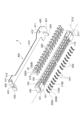
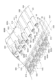
- FIG. 10 is an exploded perspective view of the connector 3, and FIG. 11 is a partially enlarged view of FIG. 10.
- the connector 3 has a base unit 500 and a plurality of shells 600.
- the base unit 500 has a connector base 510, a plurality of insulating housings 520, and a plurality of conductive contacts 530.
- the connector base 510 has an opposing surface 511.
- the opposing surface 511 faces the outer circumference of the ends of the multiple cables 20 arranged along the arrangement direction D21.
- the multiple insulating housings 520 correspond to the multiple cables 20, respectively.
- the multiple insulating housings 520 are lined up along the arrangement direction D21, and each protrudes in a direction away from the end of the corresponding cable 20 along a mating direction D22 that is parallel to the opposing surface 511 and perpendicular to the arrangement direction D21.
- the multiple insulating housings 520 are mated with the insulating housing 100 along the mating directions D12 and D22 with the mating direction D12 and the mating direction D22 coinciding.
- the multiple insulating housings 520 are each mated with the space between the multiple protrusions 110 and the receding surface 102.
- the direction in which the opposing surface 511 faces will be referred to as “upward” and the opposite direction as “downward”.
- the direction in which the multiple insulating housings 520 protrude from the connector base 510 will be referred to as “forward” and the opposite direction as “rearward”.
- the multiple cables 20 will extend rearward from the connector base 510.
- the multiple contacts 530 include multiple pairs of contacts 530 corresponding to the multiple insulating housings 520, respectively. Each of the multiple pairs of contacts 530 is held in the corresponding insulating housing 520, and contacts each of the multiple pairs of contacts 200 when the insulating housing 520 is fitted into the insulating housing 100. Each of the multiple pairs of contacts 530 is connected to the pair of signal conductors 24 described above.
- the multiple shells 600 correspond to the multiple insulating housings 520, respectively.
- Each of the multiple shells 600 is held in the insulating housing 520, and when the insulating housing 520 is fitted into the insulating housing 100, it cooperates with the shell 300 to form an enclosure that surrounds the contacts 200 and 530 around an axis along the fitting directions D12, D22.
- the enclosure will be described in more detail below.
- the connector 3 includes multiple sets of signal transmission parts TP2 corresponding to the multiple insulating housings 520, respectively.
- the multiple sets of signal transmission parts TP2 are arranged along the arrangement direction D21, and each transmits the multiple types of signals described above.
- a more detailed configuration example is given for the two sets of signal transmission parts TP2, the first and second from the right in the illustration (illustrated in Figures 10 and 11), which are representative of the multiple sets of signal transmission parts TP2.
- the first signal transmission part TP2 from the right in the illustration corresponds to the first signal transmission part TP1 from the left in Figure 7.
- the second signal transmission part TP2 from the right in the illustration corresponds to the second signal transmission part TP1 from the left in Figure 7.
- the signal transmission parts TP2 have the same configuration, for ease of explanation, the insulating housing 520, contacts 530, and shell 600 belonging to the first signal transmission part TP2 from the right in FIG. 11 are distinguished from one another as the first insulating housing 520A, first contacts 530A, and first shell 600A, and the insulating housing 520, contacts 530, and shell 600 belonging to the second signal transmission part TP2 from the right are distinguished from one another as the second insulating housing 520B, second contacts 530B, and second shell 600B.
- the cable 20 corresponding to the first signal transmission part TP2 from the right is distinguished from one another as the first cable 20A
- the cable 20 belonging to the second signal transmission part TP2 from the right is distinguished from one another as the second cable 20B.
- the first insulating housing 520A and the second insulating housing 520B are aligned along the arrangement direction D21 and protrude forward from the connector base 510 along the mating direction D22.
- the first contact 530A and the second contact 530B are electrically connected to a pair of electric wires 21.
- the first contact 530A is electrically connected to the signal conductor 24 of the electric wire 21 of the first cable 20A
- the second contact 530B is electrically connected to the signal conductor 24 of the electric wire 21 of the second cable 20B.
- the pair of first contacts 530A are held in the first insulating housing 520A and are each connected to the signal conductors 24 of the pair of electric wires 21 of the first cable 20A.
- Each of the pair of first contacts 530A has a connection portion 531 (first connection portion) and a contact portion 532 (first contact portion) that are aligned in sequence toward the front.
- the first insulating housing 520A holds a pair of first contacts 530A so that the connection portion 531 is exposed upward and the contact portion 532 is exposed downward (see FIG. 3). This allows the signal conductor 24 to be connected to the connection portion 531 from above, and the contact portion 532 can come into contact with the first contact 200A of the mating connector (connector 2) from above (see FIG. 4).
- the outer sheath 23, the outer conductor 22, and the inner sheath 25 are removed from the portion corresponding to the connection portion 531, and the pair of exposed signal conductors 24 are each connected to the connection portion 531.
- the first contact 530A is formed, for example, by punching and bending a thin metal plate.
- the pair of second contacts 530B are held in the second insulating housing 520B so as to be aligned with the pair of first contacts 530A along the arrangement direction D21, and are each connected to the signal conductors 24 of the pair of electric wires 21 of the second cable 20B.
- Each of the pair of second contacts 530B has a connection portion 531 (second connection portion) and a contact portion 532 (second contact portion), similar to the first insulating housing 520A.
- the second insulating housing 520B holds a pair of second contacts 530B so that the connection portion 531 is exposed upward and the contact portion 532 is exposed downward (see FIG. 3). This allows the signal conductor 24 to be connected to the connection portion 531 from above, and the contact portion 532 can come into contact with the second contact 200B of the mating connector (connector 2) from above (see FIG. 4).
- the outer sheath 23, the outer conductor 22, and the inner sheath 25 are removed, and the pair of exposed signal conductors 24 are each connected to the connection portion 531.
- the first shell 600A is fixed to the connector base 510 so as to surround the first insulating housing 520A around an axis along the mating direction D22.
- the first shell 600A has a cable holding portion 610 (first cable holding portion) and a mating portion 620 (first mating portion).
- the cable holding portion 610 surrounds the first cable 20A and is fixed to the connector base 510.
- the outer sheath 23 is removed from the tip of the first cable 20A at a portion corresponding to the cable holding portion 610.
- the cable holding portion 610 surrounds the external conductor 22 exposed by removing the outer sheath 23.
- the cable holding portion 610 may surround the external conductor 22 in a circular shape, or in a polygonal shape.
- the cable holding portion 610 may surround the external conductor 22 in a rectangular shape.
- the cable holding portion 610 has a pair of side walls 611 (first base side walls) and a base portion 612 (first base).
- the pair of side walls 611 face each other along the arrangement direction D21.
- the external conductor 22 of the first cable 20A is located between the pair of side walls 611 of the first shell 600A.
- the base portion 612 extends parallel to the opposing surface 511 and connects the pair of side wall portions 611.
- the mating portion 620 extends forward from the cable holding portion 610 along the mating direction D22 to surround the first insulating housing 520A.
- the mating portion 620 may surround the first insulating housing 520A in a circular shape, or in a polygonal shape.
- the mating portion 620 may surround the first insulating housing 520A in a rectangular shape.
- the mating portion 620 has a pair of side wall portions 621 (first side wall portions) and a base portion 622 (first base portion).
- the pair of side wall portions 621 are connected to the pair of side wall portions 611.
- the base portion 622 is connected to the base portion 612 and connects the pair of side wall portions 621.
- the spacing 623 between the pair of base portions 622 is smaller than the spacing 614 between the pair of side wall portions 611 (see FIG. 12).
- the outer conductor 22 of the first cable 20A is present in the cable holding portion 610, whereas the outer conductor 22 of the first cable 20A is not present in the mating portion 620.
- the mating portion 620A fits into the upper portion of the first shell 300A.
- the pair of side wall portions 621 overlap the inner surfaces of the pair of side wall portions 310 of the first shell 300A, respectively.
- the first shell 300A complements the surrounding of the first insulating housing 520A by the mating portion 620A.
- the lower portion of the first insulating housing 520A that is not surrounded by the mating portion 620A is surrounded by the first shell 300A.
- Each of the pair of side wall portions 621 may have a resilient contact portion 624 (first resilient contact portion) (see Figures 12 and 13).
- the resilient contact portion 624 approaches the first insulating housing 520A when an external force is applied, and moves away from the first insulating housing 520A when the external force is removed.
- the resilient contact portions 624 of the pair of side wall portions 621 respectively contact the inner surfaces of the pair of side wall portions 310 of the first shell 300A. This further strengthens the encircling of the first insulating housing 520A by the fitting portion 620A, which is complemented by the first shell 300A.
- the second shell 600B is fixed to the connector base 510 so as to surround the second insulating housing 520B around an axis along the mating direction D22.
- the second shell 600B has a cable holding portion 610 (second base portion) and a mating portion 620 (second end portion) similar to the first shell 600A.
- the cable holding portion 610 surrounds the second cable 20B and is fixed to the connector base 510. Like the cable holding portion 610 of the first shell 600A, the cable holding portion 610 of the second shell 600B has a pair of side walls 611 (second base side walls) and a base portion 612 (second base base portion). At the portion of the tip of the second cable 20B that corresponds to the cable holding portion 610, the outer sheath 23 is removed. The cable holding portion 610 surrounds the outer conductor 22 exposed by removing the outer sheath 23.
- the mating portion 620 extends forward from the cable holding portion 610 along the mating direction D22 and surrounds the second insulating housing 520B. Similar to the cable holding portion 610 of the first shell 600A, the mating portion 620 of the second shell 600B has a pair of side walls 621 (second end side walls) and a base portion 622 (second end base portion).
- the mating portion 620B fits into the upper portion of the second shell 300B.
- the pair of side wall portions 621 overlap the inner surfaces of the pair of side wall portions 310 of the second shell 300B, respectively.
- the surrounding of the second insulating housing 520B by the mating portion 620B is complemented by the second shell 300B.
- the lower portion of the second insulating housing 520B that is not surrounded by the mating portion 620B is surrounded by the second shell 300B.
- each of the pair of side wall portions 621 of the second shell 600B may have an elastic contact portion 624 (second elastic contact portion).
- the connector base 510 may have a conductive base plate 512 and an insulating base housing 513.
- the base plate 512 extends along the opposing surface 511 and supports the multiple cables 20 from below.
- the base housing 513 holds the base plate 512, a first insulating housing 520A, and a second insulating housing 520B.
- the base unit 500 is formed by molding the base housing 513 and the multiple insulating housings 520 with a resin material, using insert molding with the base plate 512 and the multiple contacts 530 in place.
- the cable holding portion 610 of the first shell 600A surrounds the outer conductor 22 of the first cable 20A with a pair of side walls 611, a base portion 612, and a base plate 512, and is fixed to the base plate 512.
- the cable holding portion 610 of the second shell 600B surrounds the outer conductor 22 of the second cable 20B with a pair of side walls 611, a base portion 612, and a base plate 512, and is fixed to the base plate 512.
- the base plate 512 electrically connects the cable holding portion 610 of the first shell 600A to the cable holding portion 610 of the second shell 600B.
- the outer conductor 22 of the first cable 20A is electrically connected to the base plate 512.
- the outer conductor 22 is fixed to the base plate 512 by soldering or the like.
- the outer conductor 22 of the second cable 20B is electrically connected to the base plate 512.
- the outer conductor 22 is fixed to the base plate 512 by soldering or the like.
- the base plate 512 may have a number of fixing holes 514 corresponding to the multiple cables 20, respectively.
- the multiple fixing holes 514 are aligned along the arrangement direction D21 and penetrate the base plate 512 in the up-down direction perpendicular to the opposing surface 511.
- Each of the multiple fixing holes 514 exposes the outer conductor 22 of the corresponding cable 20 downward.
- the multiple fixing holes 514 include a first fixing hole 514A corresponding to the first cable 20A and a second fixing hole 514B corresponding to the second cable 20B.
- the first fixing hole 514A exposes the outer conductor 22 of the first cable 20A downward
- the second fixing hole 514B exposes the outer conductor 22 of the second cable 20B downward.
- each of the multiple shells 600 has a pair of side wall portions 611, so that the connector 3 has multiple pairs of side wall portions 611 aligned along the arrangement direction D21.
- the base plate 512 may have multiple pairs of shell fixing holes 515 corresponding to the multiple pairs of side wall portions 611, respectively.
- the multiple fixing holes 514 and the multiple pairs of shell fixing holes 515 are aligned in a row along the arrangement direction D21.
- one fixing hole 514 is disposed between each of the multiple pairs of shell fixing holes 515.
- Each of the multiple pairs of shell fixing holes 515 penetrates the base plate 512 in the up-down direction, exposing a corresponding pair of side wall portions 611 downward.
- the multiple pairs of side wall portions 611 and the external conductors 22 of the multiple cables 20 are exposed downward while aligned in a row. Therefore, the multiple pairs of side wall portions 611 and the external conductors 22 of the multiple cables 20 can be fixed to the base plate 512 from below by soldering or the like.
- the multiple pairs of shell fixing holes 515 include a pair of first shell fixing holes 515A that respectively correspond to a pair of side wall portions 611 of the first shell 600A, and a pair of second shell fixing holes 515B that respectively correspond to a pair of side wall portions 611 of the second shell 600B.
- the first fixing hole 514A is located between the pair of first shell fixing holes 515A
- the second fixing hole 514B is located between the pair of second shell fixing holes 515B.
- Each of the multiple pairs of side wall portions 611 may have a fixing piece 613 inserted into the corresponding shell fixing hole 515.
- each of the pair of side wall portions 611 of the first shell 600A may have a fixing piece 613 (first fixing piece) inserted into the corresponding first shell fixing hole 515A.
- Each of the pair of side wall portions 611 of the second shell 600B may have a fixing piece 613 (second fixing piece) inserted into the corresponding second shell fixing hole 515B.
- This allows the multiple shells 600 to be positioned and temporarily fixed to the base plate 512 before fixing by soldering or the like, improving the workability when fixing the multiple pairs of side wall portions 611 and the outer conductors 22 of the multiple cables 20 to the base plate 512.
- the fixing piece 613 is fixed to the base plate 512 by soldering or the like while inserted into the corresponding shell fixing hole 515.
- the connector 3 may further include an insulating outer housing 700.
- the outer housing 700 accommodates a connector base 510 to which multiple shells 600, including a first shell 600A and a second shell 600B, are fixed.
- the outer housing 700 may have a front wall portion 710 perpendicular to the mating direction D22.
- the front wall portion 710 may have multiple openings 711 corresponding to the multiple insulating housings 520, respectively.
- Each of the multiple insulating housings 520 protrudes forward from the outer housing 700 through the corresponding opening 711 while being surrounded by the shell 600.
- the multiple openings 711 include a first opening 711A corresponding to the first insulating housing 520A and a second opening 711B corresponding to the second insulating housing 520B.
- the first insulating housing 520A protrudes forward from the outer housing 700 through the first opening 711A while surrounded by the first shell 600A.
- the second insulating housing 520B protrudes forward from the outer housing 700 through the second opening 711B while surrounded by the second shell 600B.
- the connector 3 may further include an insulating separator 730 fixed to the outer housing 700 and regulating the spacing of the multiple cables 20, including the spacing between the first cable 20A and the second cable 20B.
- the separator 730 holds the multiple cables 20 from outside the outer sheath 23 behind the connector base 510.
- the connector base 510 is disposed between the front wall portion 710 and the separator 730.
- the separator 730 has multiple openings 731 corresponding to the multiple cables 20 (see Figures 2 and 3).
- the multiple openings 731 are aligned along the arrangement direction D21.
- Each of the multiple openings 731 penetrates the separator 730 along the mating direction D22.
- Each of the multiple cables 20 is held in the corresponding opening 731.
- the separator 730 can appropriately maintain the distance between the cables 20, further improving the signal transmission characteristics.
- the separator 730 can also increase the fixing strength of the multiple cables 20 to the connector 3.
- the separator 730 is formed by two-color resin molding performed with the base unit 500, the shells 600, and the outer housing 700 attached to the ends of the cables 20.
- the separator 730 may be formed by resin sealing using potting.
- the base unit 500, the shells 600, and the outer housing 700 may be attached to the ends of the cables 20 with the pre-molded separator 730 attached to the cables 20.
- the separator 730 may be molded separately into an upper member and a lower member with the openings 731 at the center, and the upper member and the lower member may be combined to sandwich the cables 20.
- the separator 730 may be attached to the base unit 500 or may be molded integrally with the base unit 500. This can further increase the fixing strength of the cables 20 to the connector 3.
- the connector 3 may further include a locking member 800.
- the locking member 800 prevents the connector 3 from coming off when it is engaged with the connector 2.
- the locking member 800 has a pair of locking portions 810 and a locking knob 820.
- the pair of locking portions 810 are held in the outer housing 700 so as to correspond to the multiple locking openings 411 (see FIG. 5) of the connector 2, respectively.
- the outer housing 700 further has a pair of lock accommodating portions 720 that open upward and backward at both ends in the arrangement direction D21, and a pair of hold bars 721 that respectively correspond to the pair of lock accommodating portions 720, and the pair of locking portions 810 are respectively accommodated in the pair of lock accommodating portions 720.
- Each of the pair of hold bars 721 is located above the rear end of the corresponding lock accommodating portion 720, and holds the locking portion 810 in the lock accommodating portion 720.
- Each of the pair of locking sections 810 has a lock base 811, a lock plate 812, and an elastic connecting section 813.
- the lock base 811 extends along the mating direction D22 and contacts the bottom surface of the lock accommodating section 720.
- the lock plate 812 extends along the mating direction D22 at a position away from the bottom surface of the lock accommodating section 720 and faces the lock base 811 in the vertical direction.
- a lock claw 814 that engages with the lock opening 411 of the connector 2 is formed on the upper surface of the lock plate 812.
- the elastic connecting section 813 connects the front end of the lock base 811 to the front end of the lock plate 812 so as to enable elastic displacement of the lock claw 814 in the vertical direction.
- the locking section 810 can switch between a locked state in which the locking claw 814 engages with the locking opening 411 and a released state in which the locking claw 814 does not engage with the locking opening 411. For example, when an external force is applied from above to the locking plate 812 to bring the locking plate 812 closer to the locking base 811, the locking claw 814 descends below the main plate section 410, and the above-mentioned released state is reached. In this state, the connector 3 is fitted into the connector 2, the locking claw 814 is positioned below the locking opening 411, the external force on the locking plate 812 is removed, and the locking plate 812 is elastically restored in a direction away from the locking base 811, whereby the locking claw 814 is positioned in the locking opening 411.
- the locking claw 814 engages with the inner circumference of the locking opening 411, and the released state is switched to the locked state.
- An external force is again applied from above to the lock plate 812, bringing the lock plate 812 closer to the lock base 811 and lowering the lock claw 814, thereby switching the lock state back to the released state.
- the lock knob 820 is an operating part for simultaneously applying an external force to the lock plates 812 of the pair of locking parts 810 to switch the locked state to the unlocked state.
- the lock knob 820 extends along the arrangement direction D21 to connect the lock plates 812 of the pair of locking parts 810, and protrudes rearward so as to hang over the multiple cables 20. By pressing the lock knob 820 down towards the multiple cables 20, an external force from above can be applied simultaneously to the lock plates 812 of the pair of locking parts 810, switching the locked state to the unlocked state.
- the lock member 800 is formed by punching and bending a thin metal plate material, etc.
- the insulating housings 520 are disposed between the pair of locking portions 810 when viewed from the front. By disposing the pair of locking portions 810 in a position that does not overlap with the insulating housings 520, it is possible to achieve both a reliable connection of the connector 3 to the connector 2 and a low profile for the connector system 1.
- This procedure includes: facing the outer periphery of the first cable 20A to the facing surface 511 and connecting the signal conductor 24 of the first cable 20A to the first contact 530A; facing the outer periphery of the second cable 20B to the facing surface 511 and connecting the signal conductor 24 of the second cable 20B to the second contact 530B; disposing the first shell 600A to surround the first insulating housing 520A around an axis along the mating direction D22 in a state in which the signal conductor 24 of the first cable 20A is connected to the first contact 530A; fixing the first shell 600A to the connector base 510; disposing the second shell 600B to surround the second insulating housing 520B around an axis along the mating direction D22 in a state in which the signal conductor 24 of the second cable 20B is connected to the second contact 530B; and fixing the second shell 600B to the connector base
- the signal conductor 24 of the first cable 20A may be connected to the first contact 530A, and the signal conductor 24 of the second cable 20B may be connected to the second contact 530B simultaneously.
- the first shell 600A may be fixed to the connector base 510, and the second shell 600B may be fixed to the connector base 510 simultaneously.
- the assembly procedure for the connector 3 may further include housing the connector base 510, to which the first shell 600A and the second shell 600B are fixed, in an insulating outer housing 700.
- Fixing the first shell 600A to the connector base 510 may include soldering the first shell 600A to the base plate 512 through the first shell fixing hole 515A and soldering the outer conductor 22 of the first cable 20A to the base plate 512 through the first fixing hole 514A
- fixing the second shell 600B to the connector base 510 may include soldering the second shell 600B to the base plate 512 through the second shell fixing hole 515B and soldering the outer conductor 22 of the second cable 20B to the base plate 512 through the second fixing hole 514B.
- the soldering of the first shell 600A to the base plate 512, the soldering of the outer conductor 22 of the first cable 20A to the base plate 512, the soldering of the second shell 600B to the base plate 512, and the soldering of the outer conductor 22 of the second cable 20B to the base plate 512 may be performed simultaneously.
- the shell 600 cooperates with the shell 300 to form an enclosure 900 that surrounds the contact 200 and the contact 530 around an axis Ax1 along the mating directions D12 and D22.
- the first shell 600A cooperates with the first shell 300A to form a first enclosure 900A
- the second shell 600B cooperates with the second shell 300B to form a second enclosure 900B.
- the first enclosure 900A surrounds the first contact 200A and the first contact 530A around a first axis Ax11 along the mating directions D12 and D22.
- the second enclosure 900B surrounds the second contact 200B and the second contact 530B around a second axis Ax12 along the mating directions D12 and D22.
- non-overlapping portion 912 the length of the portion of shell 300 that does not overlap with shell 600 and forms enclosure 900
- non-overlapping portion 913 the portion of shell 600 that does not overlap with shell 300 and forms enclosure 900
- overlapping portion 911 the total length of the portion of shell 300 and shell 600 that overlap and form enclosure 900
- the non-overlapping portion 912 includes the base portion 320 described above and a portion of the pair of side wall portions 310 (a pair of side portions 311).
- the pair of side portions 311 face each other in opposing directions (e.g., arrangement direction D11, arrangement direction D21) perpendicular to the fitting directions D12, D22.
- the base portion 320 connects the pair of side portions 311.
- the non-overlapping portion 913 includes the base portion 622 described above. The base portion 622 faces the base portion 320.
- a portion of the pair of side wall portions 310 (a pair of overlapping portions 312 each connected to the pair of side portions 311) and a pair of side wall portions 621 (a pair of mating overlapping portions) overlap at two locations aligned in the arrangement direction D11.
- the pair of side wall portions 621 face each other in the opposing direction, overlap the pair of overlapping portions 312 from the inside, and are kept in contact with the shell 300.
- the pair of side wall portions 621 are kept in contact with the shell 300 by contacting the overlapping portion 312 with the elastic contact portion 624 elastically displaced inward.
- the shell 300 includes a contact portion 313 (a portion in contact with the elastic contact portion 624) that contacts the shell 600 in the overlapping portion 911.
- the surrounding body 900 may surround the contacts 200 and 530 without any gaps, or the surrounding body 900 may have gaps in the circumferential direction.
- the overlapping portion 911 has lengths L1 and L2 along the circumferential direction.
- the non-overlapping portion 912 has length L3 along the circumferential direction.
- the non-overlapping portion 913 has length L4 along the circumferential direction.
- Length L3 is longer than the sum of lengths L1 and L2, and length L4 is longer than the sum of lengths L1 and L2.
- each of lengths L3 and L4 may occupy more than 1 ⁇ 4 of the entire circumference of the connector system of the enclosure 900.
- the shell 300 overlaps with the shell 600 in the arrangement directions D11 and D21 that intersect (e.g., are perpendicular to) the circumferential direction.
- the shell 300 may be configured to overlap with the shell 600 along the circumferential direction.
- the shell 300 shown in Figures 16 and 17 has a wall portion 371 corresponding to one of the pair of side wall portions 310, a wall portion 372 corresponding to the base portion 320, and does not have a wall portion opposite the wall portion 371.
- a slit 373 is formed in the wall portion 371 along the arrangement direction D11. The slit 373 is open toward the shell 600.
- the shell 600 has a wall portion 632 corresponding to the base portion 622, and a wall portion 631 continuing to the wall portion 632 along the circumferential direction.
- the wall portion 631 is perpendicular to the wall portion 632.
- a slit 633 is formed in the wall portion 631 along the arrangement direction D21. The slit 633 is open toward the shell 300.
- the wall portion 632 faces the wall portion 372 and is kept in contact with the shell 300 along the circumferential direction by fitting into the slit 373 of the wall portion 371.
- the wall portion 372 is kept in contact with the shell 300 along the circumferential direction by fitting into the slit 633 of the wall portion 631.
- the shell 300 overlaps with the shell 600 along the circumferential direction at the portion where the wall portion 632 fits into the slit 373 and at the portion where the wall portion 372 fits into the slit 633.
- the portion where the shell 300 and the shell 600 overlap in the circumferential direction constitutes part of the enclosure 900, so the portion where the wall portion 632 fits into the slit 373 and the portion where the wall portion 372 fits into the slit 633 both correspond to the overlapping portion 911.
- the length of the overlapping portion 911 in the circumferential direction is essentially zero.
- the inner edge of the slit 373 may be formed with a contact protrusion 374 that protrudes inward and contacts the wall portion 632 (e.g., contacts the outer surface of the wall portion 632).
- the inner edge of the slit 633 may be formed with a contact protrusion 634 that protrudes inward and contacts the wall portion 372 (e.g., contacts the outer surface of the wall portion 372).
- a connector 2 includes an insulating housing 100, a conductive contact 200 held in the insulating housing 100, and a conductive shell 300 held in the insulating housing 100 so as to be disposed around the contact 200; a mating insulating housing 520 that mates with the insulating housing 100 along a mating direction D12; a conductive mating contact 530 that is held in the mating insulating housing 520 and that comes into contact with the contact 200 when the mating insulating housing 520 is mated with the insulating housing 100; and a mating insulating housing 530 that is held in the mating insulating housing 520 and that contacts the contact 200 when the mating insulating housing 520 is mated with the insulating housing 100.
- a mating connector 3 having a conductive mating shell 600 which, when mated to the connector 100, cooperates with the shell 300 to form an enclosure 900 that surrounds the contacts 200 and the mating contacts 530 around an axis along the mating direction D12, wherein, in the circumferential direction around the axis, the respective lengths of a portion where the shell 300 forms the enclosure 900 without overlapping with the mating shell 600 and a portion where the mating shell 600 forms the enclosure 900 without overlapping with the shell 300 are longer than the overall length of a portion where the shell 300 and the mating shell 600 overlap to form the enclosure 900. It is possible to form an enclosure 900 that encloses the contact 200 and the mating contact 530 while reducing the overlapping portion between the shell 300 and the mating shell 600. This is therefore effective in achieving both reliable signal transmission and compactness.
- the connector 2 further includes a conductive second contact 200B that is held in the insulating housing 100 so as to be aligned with the contact 200 along the arrangement direction D11 perpendicular to the mating direction D12, and a conductive second shell 300B that is held in the insulating housing 100 so as to be disposed around the second contact 200B.
- the mating connector 3 includes a conductive mating second contact 530B that is held in the mating insulating housing 520 so as to be aligned with the mating contact 530 along the arrangement direction D11, and in a state in which the mating insulating housing 520 is mated with the insulating housing 100, the conductive mating second contact 530B that comes into contact with the second contact 200B and is held in the mating insulating housing 520, and the mating insulating housing 520 is held in the insulating housing 100.
- the second enclosure 900B can be configured while reducing the overlapping portion between the second shell 300B and the mating second shell 300B for the second contact 200B and the mating second contact 530B. This is therefore more effective in achieving both reliable signal transmission and compact size.
- the portion of the shell 300 that forms the surrounding body 900 without overlapping with the mating shell 600 includes a pair of side portions 311 that face each other in an opposing direction perpendicular to the mating direction D12, and a base portion connecting the pair of side portions 311, and the portion of the shell 300 that forms the surrounding body 900 without overlapping with the mating shell 300 includes a mating base portion that faces the base portion. It is also effective in reducing size.
- a connector 2 that includes a conductive shell 300 that cooperates with the mating shell 600 to form an enclosure 900 that surrounds the contacts 200 and the mating contacts 530 around an axis along the mating direction D12 when the insulating housing 100 is fitted into the mating insulating housing 520, and in the circumferential direction around the axis, the length of the portion where the shell 300 forms the enclosure 900 without overlapping with the mating shell 600 and the length of the portion where the mating shell 600 forms the enclosure 900 without overlapping with the shell 300 are longer than the total length of the portion where the shell 300 and the mating shell 600 overlap to form the enclosure 900.
- 1...connector system 2...connector, 200...contact, 100...insulating housing, 101...opposing surface, D11...arrangement direction, D12...mating direction, 200B...second contact, 300B...second shell, 3...mating connector, 520...mating insulating housing, 530...mating contact, 530B...mating second contact, 900...enclosure, 900B...second enclosure, 311...side, 312...overlapping portion, 621...mating overlapping portion, 313...contact portion, 371...wall portion, 373...slit, 372...crossing wall portion, 631...mating wall portion, 632...mating crossing wall portion, 633...mating slit.
Landscapes
- Details Of Connecting Devices For Male And Female Coupling (AREA)
- Coupling Device And Connection With Printed Circuit (AREA)
Abstract
コネクタシステム1は、コネクタ2と、コネクタ3とを備える。コネクタ2は、絶縁ハウジング100と、コンタクト200と、シェル300と、を有する。コネクタ3は、相手絶縁ハウジング520と、相手コンタクト530と、シェル300と協働して、嵌合方向D12に沿った軸線まわりにコンタクト200及び相手コンタクト530を包囲する包囲体900を構成する相手シェル600と、を有する。周方向において、相手シェル600と重ならずにシェル300が包囲体900を構成する部分と、シェル300と重ならずに相手シェル600が包囲体900を構成する部分とのそれぞれの長さが、シェル300と相手シェル600とが重なって包囲体900を構成する部分の全長よりも長い。
Description
本開示は、コネクタシステム及びコネクタに関する。
特許文献1には、プラグコネクタと連結されるリセプタクルコネクタが開示されている。プラグコネクタは、ケーブルの内部導体に接続される導電性のシグナルコンタクト部材と、シグナルコンタクト部材を包囲する導電性のシェル部とを有する。リセプタクルコネクタは、プラグコネクタのシグナルコンタクト部材に接続される導電性のコンタクト部材と、コンタクト部材を包囲し、プラグコネクタのシェル部に接続される導電性のシェル部とを有する。
本開示は、信号伝送の信頼性と、小型化との両立に有効なコネクタシステムを提供する。
本開示の一側面に係るコネクタシステムは、絶縁ハウジングと、絶縁ハウジングに保持される導電性のコンタクトと、コンタクトの周囲に配置されるように絶縁ハウジングに保持される導電性のシェルと、を有するコネクタと、嵌合方向に沿って絶縁ハウジングと嵌合する相手絶縁ハウジングと、相手絶縁ハウジングに保持され、相手絶縁ハウジングが絶縁ハウジングに嵌合した状態にて、コンタクトと接触する導電性の相手コンタクトと、相手絶縁ハウジングに保持され、相手絶縁ハウジングが絶縁ハウジングに嵌合した状態にて、シェルと協働して、嵌合方向に沿った軸線まわりにコンタクト及び相手コンタクトを包囲する包囲体を構成する導電性の相手シェルと、を有する相手コネクタと、を備え、軸線まわりの周方向において、相手シェルと重ならずにシェルが包囲体を構成する部分と、シェルと重ならずに相手シェルが包囲体を構成する部分とのそれぞれの長さが、シェルと相手シェルとが重なって包囲体を構成する部分の全長よりも長い。
シェルと相手シェルとが重なる部分を減らしつつ、コンタクト及び相手コンタクトを包囲する包囲体を構成することができる。従って、信号伝送の信頼性と、小型化との両立に有効である。
コネクタは、嵌合方向に垂直な配列方向に沿ってコンタクトと並ぶように絶縁ハウジングに保持される導電性の第二コンタクトと、第二コンタクトの周囲に配置されるように絶縁ハウジングに保持される導電性の第二シェルと、を更に有し、相手コネクタは、配列方向に沿って相手コンタクトと並ぶように相手絶縁ハウジングに保持され、相手絶縁ハウジングが絶縁ハウジングに嵌合した状態にて、第二コンタクトと接触する導電性の相手第二コンタクトと、相手絶縁ハウジングに保持され、相手絶縁ハウジングが絶縁ハウジングに嵌合した状態にて、第二シェルと協働して、嵌合方向に沿った軸線まわりに第二コンタクト及び相手第二コンタクトを包囲する第二包囲体を構成する導電性の相手第二シェルと、を更に有し、軸線まわりの周方向において、相手第二シェルと重ならずに第二シェルが第二包囲体を構成する部分と、第二シェルと重ならずに相手第二シェルが第二包囲体を構成する部分とのそれぞれの長さが、第二シェルと相手第二シェルとが重なって第二包囲体を構成する部分の全長よりも長くてもよい。第二コンタクト及び相手第二コンタクトに対しても、第二シェルと相手第二シェルとが重なる部分を減らしつつ第二包囲体を構成することができる。従って、信号伝送の信頼性と、小型化との両立に更に有効である。
コンタクト及び第二コンタクトは回路基板における第一信号ライン及び第二信号ラインに電気的に接続され、相手コンタクト及び相手第二コンタクトは一以上のケーブルの第一信号導体及び第二信号導体に電気的に接続されてもよい。回路基板が搭載される機器の小型化に有効である。
絶縁ハウジングは回路基板に対向する対向面を有し、配列方向及び嵌合方向は対向面に平行であってもよい。回路基板に対するコネクタの小型化に有効である。
シェルは、シェルと相手シェルとが重なって包囲体を構成する部分において相手シェルに接触する接触部を含んでもよい。シェルと相手シェルとの接触によって、信号伝送の信頼性を更に向上させることができる。
包囲体は、切れ目なくコンタクト及び相手コンタクトを包囲してもよい。シェルと相手シェルとの接触によって、信号伝送の信頼性を更に向上させることができる。
相手シェルと重ならずにシェルが包囲体を構成する部分の長さと、シェルと重ならずに相手シェルが包囲体を構成する部分の長さとのそれぞれが、包囲体の全周の1/4以上を占めてもよい。小型化に更に有効である。
相手シェルと重ならずにシェルが包囲体を構成する部分は、嵌合方向に垂直な対向方向において互いに対向する一対の側部と、一対の側部をつなぐベース部とを含み、シェルと重ならずに相手シェルが包囲体を構成する部分は、ベース部と対向する相手ベース部を含んでもよい。小型化に更に有効である。
シェルは、一対の側部にそれぞれ連なる一対の重複部を有し、相手シェルは、対向方向において互いに対向し、一対の重複部に対して内方からそれぞれ重なって、シェルと接触した状態に保たれる一対の相手重複部を有してもよい。信号伝送の信頼性と、小型化との両立に更に有効である。
シェルは、軸線まわりの周方向に沿って相手シェルと重なってもよい。小型化に更に有効である。
シェルは、嵌合方向に沿ったスリットが形成された壁部を有し、相手シェルは、壁部に交差してスリットにはまり込むことで、周方向に沿ってシェルと接触した状態に保たれる相手壁部を有してもよい。信号伝送の信頼性と、小型化との両立に更に有効である。
相手シェルは、相手壁部に交差する相手交差壁部を更に有し、相手交差壁部には嵌合方向に沿った相手スリットが形成され、シェルは、相手交差壁部に交差して相手スリットにはまり込むことで、周方向に沿って相手シェルと接触した状態に保たれる交差壁部を有してもよい。信号伝送の信頼性と、小型化との両立に更に有効である。
本開示の他の側面に係るコネクタは、相手絶縁ハウジングと、相手絶縁ハウジングに保持される導電性の相手コンタクトと、相手コンタクトの周囲に配置されるように相手絶縁ハウジングに保持される導電性の相手シェルと、を有する相手コネクタと接続されるコネクタであって、嵌合方向に沿って相手絶縁ハウジングと嵌合する絶縁ハウジングと、絶縁ハウジングに保持され、絶縁ハウジングが相手絶縁ハウジングに嵌合した状態にて、相手コンタクトと接触する導電性のコンタクトと、絶縁ハウジングに保持され、絶縁ハウジングが相手絶縁ハウジングに嵌合した状態にて、相手シェルと協働して、嵌合方向に沿った軸線まわりにコンタクト及び相手コンタクトを包囲する包囲体を構成する導電性のシェルと、を備え、軸線まわりの周方向において、相手シェルと重ならずにシェルが包囲体を構成する部分と、シェルと重ならずに相手シェルが包囲体を構成する部分とのそれぞれの長さが、シェルと相手シェルとが重なって包囲体を構成する部分の全長よりも長い。
本開示によれば、信号伝送の信頼性と、小型化との両立に有効なコネクタシステムを提供することができる。
以下、実施形態について、図面を参照しつつ詳細に説明する。説明において、同一要素又は同一機能を有する要素には同一の符号を付し、重複する説明を省略する。
〔コネクタシステム〕
図1及び図2に示すコネクタシステム1は、高周波信号を低い劣化で伝送することと、低背化とが求められる用途において、回路基板10(図3に示される)と、複数のケーブル20との接続に用いられる。このような用途の一例として、回路基板10上のプリント配線の代わりに、複数のケーブル20によって回路基板10上の信号伝送を行う情報処理システムが挙げられる。複数のケーブル20のそれぞれをシールドケーブルとすること等によって、プリント配線よりも高い信号伝送特性で信号を伝送することができる。信号伝送特性とは、信号伝送における信号劣化の少なさを意味し、信号伝送特性が高いとは、信号伝送における信号劣化が少ないことを意味する。信号劣化の具体例としては、クロストーク等によるノイズの混入及び信号の減衰等が挙げられる。
図1及び図2に示すコネクタシステム1は、高周波信号を低い劣化で伝送することと、低背化とが求められる用途において、回路基板10(図3に示される)と、複数のケーブル20との接続に用いられる。このような用途の一例として、回路基板10上のプリント配線の代わりに、複数のケーブル20によって回路基板10上の信号伝送を行う情報処理システムが挙げられる。複数のケーブル20のそれぞれをシールドケーブルとすること等によって、プリント配線よりも高い信号伝送特性で信号を伝送することができる。信号伝送特性とは、信号伝送における信号劣化の少なさを意味し、信号伝送特性が高いとは、信号伝送における信号劣化が少ないことを意味する。信号劣化の具体例としては、クロストーク等によるノイズの混入及び信号の減衰等が挙げられる。
複数のケーブル20による信号伝送特性を更に高めるためには、回路基板10と複数のケーブル20との接続箇所を、回路基板10上の回路素子(例えばプロセッサ)に近付けることが必要となる。回路基板10と複数のケーブル20との接続箇所を回路素子の近傍に設けるためには、回路素子に設けられるヒートシンク等との干渉を避ける必要がある。このため、コネクタシステム1の低背化が必要とされる。
コネクタシステム1は、コネクタ2と、コネクタ3とを備える。コネクタ2は、例えばリセプタクルコネクタであり、回路基板10に接続される。コネクタ3は、例えばプラグコネクタであり、複数のケーブル20に接続される。コネクタ3をコネクタ2に接続可能である。コネクタ3をコネクタ2に接続することによって、複数のケーブル20が回路基板10に電気的に接続される。コネクタ2とコネクタ3とは、回路基板10に平行な嵌合方向D12に沿って互いに嵌合する。以下、コネクタ3をコネクタ2に対する「相手コネクタ」と称する場合があるが、必ずしもコネクタ3のみが「相手コネクタ」に該当するわけではなく、コネクタ2はコネクタ3に対する「相手コネクタ」である。
コネクタ2は、複数のコンタクト200と、複数のシェル300と、絶縁ハウジング100とを備える。複数のコンタクト200は、回路基板10の主面に平行で嵌合方向D12に垂直な配列方向D11に沿って並ぶように絶縁ハウジング100に保持される。複数のコンタクト200のそれぞれは、回路基板10に電気的に接続され、相手コネクタ(コネクタ3)の信号コンタクトに接触する。複数のシェル300のそれぞれは、少なくとも一つのコンタクト200の周囲に配置されるように絶縁ハウジング100に保持される。例えば複数のシェル300のそれぞれは、嵌合方向D12に沿った軸線まわりに少なくとも一つのコンタクト200を包囲するように絶縁ハウジング100に保持される。
複数のコンタクト200は複数種類の信号を伝送する。複数のシェル300は、複数種類の信号ごとに設けられていてもよい。この場合、複数のシェル300のそれぞれが包囲する領域においては、一種類の信号のみが伝送され、他の信号は伝送されない。一例として、複数のコンタクト200のそれぞれが、グランド電位を基準とする一種類の信号を伝送してもよい。この場合、複数のシェル300は複数のコンタクト200ごとに設けられる。複数のシェル300のそれぞれは一つのコンタクト200のみを包囲し、他のコンタクト200を包囲しない。複数のコンタクト200は、複数種類の差動信号をそれぞれ伝送する複数対のコンタクト200を含んでいてもよい。この場合、複数のシェル300は複数対のコンタクト200ごとに設けられる。複数のシェル300のそれぞれは、一対のコンタクト200のみを包囲し、他のコンタクト200を包囲しない。
絶縁ハウジング100は、複数のコンタクト200と、複数のシェル300とを一体的に保持する。絶縁ハウジング100は、複数のコンタクト200同士を互いに絶縁された状態に保ち、複数のシェル300同士を互いに絶縁された状態に保ち、複数のコンタクト200と複数のシェル300とを互いに絶縁された状態に保つ。
コネクタ3は、図1及び図10に示されるように、ベースユニット500と、複数のシェル600とを備える。ベースユニット500は、コネクタベース510と、絶縁性の複数の絶縁ハウジング520と、導電性の複数のコンタクト530とを有する。コネクタベース510は、配列方向D11(D21)に沿って延びる。複数の絶縁ハウジング520は配列方向D11に沿って並び、それぞれ嵌合方向D12(D22)に沿ってコネクタベース510から互いに同じ方向に向かって突出している。
複数のコンタクト530は、配列方向D11に沿って並ぶように複数の絶縁ハウジング520に保持される。複数のコンタクト530のそれぞれは、複数のケーブル20のいずれかに電気的に接続され、相手コネクタ(コネクタ2)のコンタクト200に接触する。複数の絶縁ハウジング520のそれぞれは、少なくとも一つのコンタクト530を保持する。
複数のコンタクト530は上述の複数種類の信号を伝送し、複数の絶縁ハウジング520は、複数種類の信号ごとに設けられていてもよい。この場合、複数の絶縁ハウジング520においては、一種類の信号のみが伝送され、他の信号は伝送されない。一例として、複数のコンタクト530のそれぞれが、グランド電位を基準とする一種類の信号を伝送してもよい。この場合、複数の絶縁ハウジング520は複数のコンタクト530ごとに設けられる。複数の絶縁ハウジング520のそれぞれは一つのコンタクト530のみを保持し、他のコンタクト530を保持しない。複数のコンタクト530は、複数種類の差動信号をそれぞれ伝送する複数対のコンタクト530を含んでいてもよい。この場合、複数の絶縁ハウジング520は複数対のコンタクト530ごとに設けられる。複数の絶縁ハウジング520のそれぞれは、一対のコンタクト530のみを保持し、他のコンタクト530を保持しない。
複数のシェル600は、複数の絶縁ハウジング520にそれぞれ対応する。複数のシェル600のそれぞれは、対応する絶縁ハウジング520を嵌合方向D12(D22)に沿った軸線まわりに包囲する。
複数の絶縁ハウジング520は、複数のシェル300にそれぞれ対応する。図3及び図4に示すように、複数の絶縁ハウジング520のそれぞれは、嵌合方向D12に沿って、対応するシェル300に挿入される。複数のシェル600のそれぞれは、嵌合方向D12に沿って、対応するシェル300に嵌合する。複数のコンタクト530のそれぞれは、対応するシェル300内において、対応するコンタクト200に接触する。これにより、複数のケーブル20が回路基板10に電気的に接続される。
このコネクタシステム1によれば、複数のコンタクト200に個別のシェル300を設けることによって、コンタクト200とシェル300との関係を個別に最適化することができる。また、シェル300は、回路基板10に平行な嵌合方向D12に沿った軸線まわりにコンタクト200を包囲する。これにより、コネクタ2に対するコネクタ3の嵌合方向が、回路基板10に平行な方向に規制される。このため、コネクタ2とコネクタ3とにより構成される接続部の低背化(回路基板10の表面に対する低背化)を図ることができる。従って、信号伝送特性の向上と、低背化との両立に有効である。
低背化によって、例えば図3及び図4に示すように、ヒートシンク12等との干渉を避け、回路素子11の近傍にコネクタ2を配置することが可能となるので、信号伝送特性の更なる向上を図ることができる。
複数のシェル300のそれぞれは、対応するシェル600による絶縁ハウジング520の包囲を補完してもよい。例えば、絶縁ハウジング520の周囲のうち、シェル600により包囲されていない部分をシェル300が包囲してもよい。これにより、シェル600とシェル300との重複を削減することで、更なる低背化が可能となる。
以下、コネクタ2及びコネクタ3のそれぞれの構成をより詳細に例示する。
〔第一コネクタ〕
コネクタ2の説明においては、便宜上、回路基板の表面に向かう方向を「下方」とし、回路基板の表面から離れる方向を「上方」とする。図5は、コネクタ2を下方から見た斜視図であり、図6は、図5中のコネクタ2を分解して示す斜視図である。図5に示すように、コネクタ2は、絶縁性の絶縁ハウジング100と、導電性の複数のコンタクト200と、導電性の複数のシェル300とを有する。
コネクタ2の説明においては、便宜上、回路基板の表面に向かう方向を「下方」とし、回路基板の表面から離れる方向を「上方」とする。図5は、コネクタ2を下方から見た斜視図であり、図6は、図5中のコネクタ2を分解して示す斜視図である。図5に示すように、コネクタ2は、絶縁性の絶縁ハウジング100と、導電性の複数のコンタクト200と、導電性の複数のシェル300とを有する。
図6及び図7に示されるように、絶縁ハウジング100は、対向面101と、後退面102と、複数の凸部110とを有する。対向面101は、回路基板10に対向する。配列方向D11及び嵌合方向D12は対向面101に平行である。後退面102は、対向面101が回路基板10に対向した状態にて、回路基板10から離れた位置で回路基板10に対向する。複数の凸部110は、対向面101に平行な配列方向D11に沿って並び、それぞれ後退面102から突出している。
複数の凸部110は、複数のシェル300にそれぞれ対応する。複数のシェル300のそれぞれは、対応する凸部110に保持される。また、複数のシェル300のそれぞれが包囲する少なくとも一つのコンタクト200も凸部110に保持される。例えば、複数のシェル300のそれぞれが包囲する一対のコンタクト200が、配列方向D11に沿って並ぶように凸部110に保持される。絶縁ハウジング100は、樹脂材料の成型等により形成される。
一箇所の凸部110と、これに対応するシェル300及び一対のコンタクト200は、一セットの信号伝送部TP1を構成する。コネクタ2は、複数の凸部110にそれぞれ対応する複数セットの信号伝送部TP1を含む。複数セットの信号伝送部TP1は、配列方向D11に沿って並び、上述した複数種類の信号をそれぞれ伝送する。以下、複数セットの信号伝送部TP1を代表して、図示左側から一番目と二番目の二セットの信号伝送部TP1について、より詳細に構成を例示する。
複数セットの信号伝送部TP1の構成は共通であるが、説明の便宜上、図示左側から一番目の信号伝送部TP1に属する凸部110、コンタクト200及びシェル300を第一凸部110A、第一コンタクト200A及び第一シェル300Aとし、図示左側から二番目の信号伝送部TP1に属する凸部110、コンタクト200及びシェル300を第二凸部110B、第二コンタクト200B及び第二シェル300Bとして互いに区別する。
特に図7に示すように、第一コンタクト200Aと、第二コンタクト200Bとは、配列方向D11に沿って並ぶように絶縁ハウジング100に保持される。第一コンタクト200Aと第二コンタクト200Bとは、回路基板10における一対の信号ライン13に電気的に接続される。第一コンタクト200Aと第二コンタクト200Bとがそれぞれ接続される「一対の信号ライン13」は、互いに別の信号を伝送する。第一凸部110Aが一対の第一コンタクト200Aを含み、第二凸部110Bが一対の第二コンタクト200Bを含む場合には、例えば、一対の第一コンタクト200Aが配列方向D11に沿って並ぶように第一凸部110Aに保持され、一対の第二コンタクト200Bが配列方向D11に沿って並ぶように第二凸部110Bに保持され、第一凸部110Aと第二凸部110Bとの配列に対応して、一対の第一コンタクト200Aと一対の第二コンタクト200Bとが配列方向D11に沿って並んでいる。
一対の第一コンタクト200Aは、回路基板10において第一差動信号を伝送する一対の信号ライン13に電気的に接続される。一対の第二コンタクト200Bは、回路基板10において第一差動信号とは別の第二差動信号を伝送する一対の信号ライン13に電気的に接続される。
一対の第一コンタクト200Aのそれぞれは、接続部201(第一接続部)と、接触部202(第一接触部)とを有する。接続部201は、回路基板10に電気的に接続される。例えば接続部201は、回路基板10に形成された導電性の信号ターミナルに半田付け等によって接続される。接触部202は、対向面101に平行で配列方向D11に垂直な嵌合方向D12に沿って接続部201から突出している。以下、説明の便宜上、接続部201に対する接触部202の突出方向を「前方」といい、その反対方向を「後方」という。 第一コンタクト200Aは、接触部202が回路基板10から離れて位置するように、接続部201と接触部202との間でクランク状に屈曲している。第一コンタクト200Aは、例えば金属の薄板材の打ち抜き及び曲げ加工等により形成される。
一対の第二コンタクト200Bのそれぞれは、第一コンタクト200Aと同様に構成され、接続部201(第二接続部)と、接触部202(第二接続部)とを有する。第二コンタクト200Bの接続部201は、第一コンタクト200Aの接続部201が接続される信号ターミナルとは別個に回路基板10に形成された導電性の信号ターミナルに半田付け等によって接続される。
第一シェル300Aは、一対の第一コンタクト200Aの周囲に配置されるように絶縁ハウジング100に保持される。例えば第一シェル300Aは、嵌合方向D12に沿った軸線まわりに一対の第一コンタクト200Aを包囲するように絶縁ハウジング100に保持され、対向面101が回路基板10に対向した状態にて、回路基板10に電気的に接続される。
嵌合方向D12において、第一シェル300Aは一対の第一コンタクト200Aを部分的に包囲していてもよい。例えば第一シェル300Aは、少なくとも一対の第一コンタクト200Aの接触部202を包囲する。
第一シェル300A内においては、少なくとも一つの第一コンタクト200Aにより伝送される一種類の信号以外の信号は伝送されない。当該一種類の信号が、第一シェル300A内で伝送される唯一の信号である。例えば、第一シェル300A内においては、上記第一差動信号のみが伝送され、他の信号は伝送されない。第一シェル300Aは一対の第一コンタクト200Aのみを包囲し、他のコンタクト200を包囲しない。
一対の第一コンタクト200Aを包囲する形状に特に制限はない。第一シェル300Aは、一対の第一コンタクト200Aを円形状に包囲してもよく、一対の第一コンタクト200Aを多角形状に包囲してもよい。一例として、第一シェル300Aは、第一コンタクト200Aを矩形状に包囲してもよい。例えば第一シェル300Aは、一対の側壁部310(第一側壁部)と、ベース部320(第一ベース部)とを有する(図8参照)。
一対の側壁部310は、配列方向D11に沿って互いに対向する。一対の第一コンタクト200Aの接触部202は、一対の側壁部310の間に位置する。ベース部320は、対向面101に平行に広がって一対の側壁部310を連結する。対向面101が回路基板10に対向した状態にて、ベース部320は接触部202と回路基板10との間に位置してもよい。
図6に示されるように、一対の側壁部310の間には、受入空間IS(第一受入空間)が形成される。受入空間ISには、嵌合方向D12に沿って、相手コネクタ(コネクタ3)の相手第一ハウジング(複数の絶縁ハウジング520のいずれか一つ)が挿入される。相手コネクタの相手シェル(シェル600A)が第一シェル300Aに嵌合し、相手第一ハウジングに保持された相手信号コンタクト(コンタクト530A)が第一コンタクト200Aの接触部202に接触する(図4参照)。例えば、一対のコンタクト530Aが、一対の第一コンタクト200Aの接触部202にそれぞれ接触する。
図8に示されるように、第一シェル300Aは、後方に向かって一対の側壁部310からそれぞれ張り出した一対の張出部340(第一張出部)を更に有してもよい。一対の第一コンタクト200Aの接続部201は、一対の張出部340の間に位置する。
第一シェル300Aは、対向面101が回路基板10に対向した状態にて、回路基板10に電気的に接続されるように一対の張出部340にそれぞれ形成された一対のシェル接続部341(第一シェル接続部)を更に有してもよい。例えば一対のシェル接続部341のそれぞれは、対応する張出部340の下縁に形成され、上述の信号ターミナルとは別個に回路基板10に形成された導電性のグランドターミナルに半田付け等によって接続される。回路基板10において、グランドターミナルにはグランド電位が付与される。以下、シェル接続部341の他の部分が接続されるグランドターミナルについても同様である。
第一シェル300Aは、アンカー部350(第一アンカー部)と、中間接続部360(第一中間接続部)とを更に有してもよい(図9参照)。アンカー部350は、ベース部320から後方に向かって張り出して第一凸部110Aに保持される。中間接続部360は、対向面101が回路基板10に対向した状態にて、回路基板10に電気的に接続されるようにベース部320に形成されている。例えば中間接続部360は、アンカー部350の後端部に形成されており、後退面102から離れる方向に向かってアンカー部350の後端部から突出している。一例として、中間接続部360は、アンカー部350の後端部から後方及び下方に向かって突出し、回路基板10に形成されたグランドターミナルに半田付け等によって接続される。
第一シェル300Aは、例えば金属の薄板の打ち抜き及び曲げ加工により形成される。
第二シェル300Bは、一対の第二コンタクト200Bの周囲に配置されるように絶縁ハウジング100に保持される。第二シェル300Bは、嵌合方向D12に沿った軸線まわりに一対の第二コンタクト200Bを包囲するように絶縁ハウジング100に保持され、対向面101が回路基板10に対向した状態にて、回路基板10に電気的に接続される。例えば第二シェル300Bは、少なくとも一対の第二コンタクト200Bの接触部202を包囲する。第二シェル300B内においては、少なくとも一つの第二コンタクト200Bにより伝送される一種類の信号以外の信号は伝送されない。当該一種類の信号が、第二シェル300B内で伝送される唯一の信号である。例えば、第二シェル300B内においては、上記第二差動信号のみが伝送され、他の信号は伝送されない。第二シェル300Bは一対の第二コンタクト200Bのみを包囲し、他のコンタクト200を包囲しない。
第二シェル300Bは、第一シェル300Aと同様に構成され、一対の側壁部310(第二側壁部)と、ベース部320(第二ベース部)とを有する。一対の第二コンタクト200Bの接触部202は、一対の側壁部310の間に位置する。
一対の側壁部310の間には、受入空間IS(第二受入空間)が形成される。受入空間ISには、嵌合方向D12に沿って、相手コネクタ(コネクタ3)の相手第二ハウジング(複数の絶縁ハウジング520のいずれか一つ)が挿入される。相手第二ハウジングを包囲する相手シェル(シェル600B)が第二シェル300Bに嵌合し、相手第二ハウジングに保持された相手信号コンタクト(コンタクト530B)が第二コンタクト200Bの接触部202に接触する(図4参照)。例えば、一対のコンタクト530Bが、一対の第二コンタクト200Bの接触部202にそれぞれ接触する。
第一シェル300Aと同様に、第二シェル300Bは、一対の張出部340(第二張出部)と、一対のシェル接続部341を更に有してもよい。一対の第二コンタクト200Bの接続部201は、一対の張出部340の間に位置する。第一シェル300Aの一対のシェル接続部341と同様に、第二シェル300Bの一対のシェル接続部341は、回路基板10に形成されたグランドターミナルに半田付け等によって接続される。
第一シェル300Aと同様に、第二シェル300Bは、アンカー部350と、中間接続部360とを更に有してもよい。アンカー部350は、ベース部320から後方に張り出して第二凸部110Bに保持される。中間接続部360は、回路基板10に形成されたグランドターミナルに半田付け等によって接続される。
図7に示されるように、第一凸部110Aは、後退面102から突出して第一シェル300Aの一対の張出部340の間に位置し、一対の第一コンタクト200Aと第一シェル300Aとを保持する。例えば第一凸部110Aは、一対のコンタクト保持孔111(第一凸部110Aの上方に位置する)と、アンカー孔112とを有する。一対のコンタクト保持孔111は、配列方向D11に沿って並び、それぞれ嵌合方向D12に沿って第一凸部110Aを貫通している。一対のコンタクト保持孔111には、後方から一対の第一コンタクト200Aの接触部202がそれぞれ挿入される。一対の第一コンタクト200Aの接触部202の端部は、第一凸部110Aから前方に突出し、第一シェル300Aに包囲される。アンカー孔112は、一対のコンタクト保持孔111よりも下方に位置し、嵌合方向D12に沿って第一凸部110Aを貫通している。アンカー孔112には、前方から第一シェル300Aのアンカー部350が挿入される。
第一凸部110Aには、スリット113(第一スリット)が形成されていてもよい。スリット113は、嵌合方向D12に沿った中間接続部360の変位を許容する。例えばスリット113は、嵌合方向D12に沿い、アンカー孔112の下部の全長に亘って形成されており、スリット113内に中間接続部360が配置される。スリット113が嵌合方向D12に沿って延びているため、嵌合方向D12に沿った中間接続部360の変位が許容される。
絶縁ハウジング100は、第一支持部114Aを更に有してもよい。第一支持部114Aは、第一凸部110Aから前方に向かって張り出して接触部202とベース部320との間に位置する。例えば第一支持部114Aは、一対のコンタクト保持孔111とアンカー孔112との間において、第一凸部110Aから前方に向かって張り出している。
第二凸部110Bは、後退面102から突出して第二シェル300Bの一対の張出部340の間に位置し、一対の第二コンタクト200Bと第二シェル300Bとを保持する。例えば第二凸部110Bは、第一凸部110Aと同様に、一対のコンタクト保持孔111(第二凸部110Bの上方に位置する)と、アンカー孔112とを有する。一対のコンタクト保持孔111には、後方から一対の第二コンタクト200Bの接触部202がそれぞれ挿入される。一対の第二コンタクト200Bの接触部202の端部は、第二凸部110Bから前方に突出し、第二シェル300Bに包囲される。アンカー孔112には、前方から第二シェル300Bのアンカー部350が挿入される。第一凸部110Aと同様に、第二凸部110Bにはスリット113(第二スリット)が形成されていてもよい。スリット113内には、第二シェル300Bの中間接続部360が配置される。
絶縁ハウジング100は、第一支持部114Aと同様の第二支持部114Bを更に有してもよい。第二支持部114Bは、第二凸部110Bから前方に向かって張り出して接触部202とベース部320との間に位置する。例えば第二支持部114Bは、一対のコンタクト保持孔111とアンカー孔112との間において、第二凸部110Bから前方に向かって張り出している。
図5及び図6に戻り、コネクタ2は、導電性のアウターシェル400を更に備えてもよい。絶縁ハウジング100は、対向面101の裏面103を有し、アウターシェル400は裏面103を覆う。
例えばアウターシェル400は、主板部410と、一対のアウター側壁部420と、一対のアンカー部430とを有し、金属の薄板材の打ち抜き及び曲げ加工等により形成される。主板部410は、裏面103の少なくとも一部を覆うように広がっている。一対のアウター側壁部420は、配列方向D11における主板部410の両端部にそれぞれ設けられている。例えば一対のアウター側壁部420は、主板部410の両端部において、主板部410に対して下方に屈曲し、配列方向D11に沿って互いに対向している。一対のアンカー部430も、配列方向D11における主板部410の両端部にそれぞれ設けられており、一対のアウター側壁部420よりも後方に位置している。例えば一対のアンカー部430は、主板部410の両端部において、主板部410に対して下方に屈曲し、配列方向D11に沿って互いに対向している。前方から見て、複数のシェル300は、一対のアウター側壁部420の間に位置し、一対のアンカー部430の間にも位置する。
一対のアンカー部430は、絶縁ハウジング100に保持される。例えば絶縁ハウジング100は、一対のアンカー部430にそれぞれ対応する一対のアウター保持孔121を更に有する。一対のアウター保持孔121のそれぞれは、絶縁ハウジング100を上下に貫通している。一対のアンカー部430は、上方から一対のアウター保持孔121にそれぞれ挿入される。
一対のアウター側壁部420は、絶縁ハウジング100の前面よりも前方に張り出していてもよい。これにより、嵌合方向D12に沿ってコネクタ3がスムーズにガイドされる。
主板部410の両端部には、絶縁ハウジング100の前面よりも前方に張り出す一対の張出部412がそれぞれ形成されており、一対の張出部412には一対のロック開口411がそれぞれ形成されている。一対のロック開口411のそれぞれは、下方から見て、複数のシェル300と、一対のアウター側壁部420との間にそれぞれ位置している。一対のロック開口411には、後述するコネクタ3の一対のロック爪814がそれぞれ係合する。
アウターシェル400は、一対のアウター接続部421を更に有してもよい。一対のアウター接続部421は、対向面101が回路基板10に対向した状態にて、回路基板10に電気的に接続されるように、一対のアウター側壁部420にそれぞれ形成されている。例えば一対のアウター接続部421のそれぞれは、対応するアウター側壁部420の下縁に形成され、回路基板10に形成されたグランドターミナルに半田付け等によって接続される。
〔第二コネクタ〕
上述したように、コネクタ3は、複数のケーブル20に接続される。特に図11に示されるように、複数のケーブル20のそれぞれは、少なくとも一本の信号導体24を有する。一本のケーブル20は、一種類の信号を伝送する。例えばケーブル20は、一種類の差動信号を伝送する。例えば、一本のケーブル20は、一対の電線21と、外部導体22と、絶縁性のアウターシース23とを有する。一対の電線21のそれぞれは、一本の信号導体24と、信号導体24を被覆する絶縁性のインナーシース25とを有する。以下、一対の電線21の信号導体24を、一対の信号導体24という。一対の信号導体24によって、上述の差動信号が伝送される。外部導体22は、一対の電線21を包囲し、アウターシース23は外部導体22を被覆する。
上述したように、コネクタ3は、複数のケーブル20に接続される。特に図11に示されるように、複数のケーブル20のそれぞれは、少なくとも一本の信号導体24を有する。一本のケーブル20は、一種類の信号を伝送する。例えばケーブル20は、一種類の差動信号を伝送する。例えば、一本のケーブル20は、一対の電線21と、外部導体22と、絶縁性のアウターシース23とを有する。一対の電線21のそれぞれは、一本の信号導体24と、信号導体24を被覆する絶縁性のインナーシース25とを有する。以下、一対の電線21の信号導体24を、一対の信号導体24という。一対の信号導体24によって、上述の差動信号が伝送される。外部導体22は、一対の電線21を包囲し、アウターシース23は外部導体22を被覆する。
図10は、コネクタ3を分解して示す斜視図であり、図11は、図10の部分拡大図である。図10に示すように、コネクタ3は、ベースユニット500と、複数のシェル600とを有する。図11に示すように、ベースユニット500は、コネクタベース510と、絶縁性の複数の絶縁ハウジング520と、導電性の複数のコンタクト530とを有する。
コネクタベース510は、対向面511を有する。対向面511は、配列方向D21に沿って配列された複数のケーブル20の端部の外周に対向する。複数の絶縁ハウジング520は、複数のケーブル20にそれぞれ対応する。複数の絶縁ハウジング520は、配列方向D21に沿って並び、それぞれ対向面511に平行で配列方向D21に垂直な嵌合方向D22に沿って、対応するケーブル20の端部から遠ざかる方向に突出する。複数の絶縁ハウジング520は、嵌合方向D12と嵌合方向D22とが一致した状態にて、嵌合方向D12,D22に沿って絶縁ハウジング100と嵌合する。例えば複数の絶縁ハウジング520は、複数の凸部110と後退面102との間の空間にそれぞれ嵌合する。
以下、説明の便宜上、対向面511が面する方向を「上方」とし、その反対方向を「下方」とする。また、複数の絶縁ハウジング520がコネクタベース510から突出する方向を「前方」とし、その反対方向を「後方」とする。この定義によれば、複数のケーブル20が、コネクタベース510から後方に延びることとなる。コネクタ3がコネクタ2に嵌合した状態において、コネクタ2の説明における上下と、コネクタ3の説明における上下とは一致することとなる。また、コネクタ3の説明における前方はコネクタ2の説明における後方に対応し、コネクタ3の説明における後方はコネクタ2の説明における前方に対応する。
複数のコンタクト530は、複数の絶縁ハウジング520にそれぞれ対応する複数対のコンタクト530を含む。複数対のコンタクト530のそれぞれは、対応する絶縁ハウジング520に保持され、絶縁ハウジング520が絶縁ハウジング100に嵌合した状態にて、複数対のコンタクト200とそれぞれ接触する。複数対のコンタクト530のそれぞれには、上述した一対の信号導体24がそれぞれ接続される。
複数のシェル600は、複数の絶縁ハウジング520にそれぞれ対応する。複数のシェル600のそれぞれは、絶縁ハウジング520に保持され、絶縁ハウジング520が絶縁ハウジング100に嵌合した状態にて、シェル300と協働して、嵌合方向D12,D22に沿った軸線まわりにコンタクト200及びコンタクト530を包囲する包囲体を構成する。包囲体についてはより詳細に後述する。
コネクタ3は、複数の絶縁ハウジング520にそれぞれ対応する複数セットの信号伝送部TP2を含む。複数セットの信号伝送部TP2は、配列方向D21に沿って並び、上述した複数種類の信号をそれぞれ伝送する。以下、複数セットの信号伝送部TP2を代表して、図示(図10及び図11における図示)の右側から一番目と二番目の二セットの信号伝送部TP2について、より詳細に構成を例示する。なお、図示右側から一番目の信号伝送部TP2は、図7における左側から一番目の信号伝送部TP1に対応する。図示右側から二番目の信号伝送部TP2は、図7における左側から二番目の信号伝送部TP1に対応する。
複数の信号伝送部TP2の構成は共通であるが、説明の便宜上、図11における右側から一番目の信号伝送部TP2に属する絶縁ハウジング520、コンタクト530及びシェル600を第一絶縁ハウジング520A、第一コンタクト530A及び第一シェル600Aとし、右側から二番目の信号伝送部TP2に属する絶縁ハウジング520、コンタクト530及びシェル600を第二絶縁ハウジング520B、第二コンタクト530B及び第二シェル600Bとして互いに区別する。また、右側から一番目の信号伝送部TP2に対応するケーブル20を第一ケーブル20Aとし、右側から二番目の信号伝送部TP2に属するケーブル20を第二ケーブル20Bとして互いに区別する。
第一絶縁ハウジング520A及び第二絶縁ハウジング520Bは、配列方向D21に沿って並び、嵌合方向D22に沿ってコネクタベース510から前方に向かって突出している。
図11に示されるように、第一コンタクト530Aと第二コンタクト530Bとは、一対の電線21に電気的に接続される。例えば第一コンタクト530Aは、第一ケーブル20Aの電線21の信号導体24に電気的に接続され、第二コンタクト530Bは、第二ケーブル20Bの電線21の信号導体24に電気的に接続される。一対の第一コンタクト530Aは、第一絶縁ハウジング520Aに保持され、第一ケーブル20Aの一対の電線21の信号導体24にそれぞれ接続される。一対の第一コンタクト530Aのそれぞれは、前方に向かって順に並ぶ接続部531(第一接続部)と接触部532(第一接触部)とを有する。
第一絶縁ハウジング520Aは、接続部531を上方に露出させ、接触部532を下方に露出させるように、一対の第一コンタクト530Aを保持する(図3参照)。これにより、接続部531に対して上方から信号導体24を接続することが可能であり、接触部532は相手コネクタ(コネクタ2)の第一コンタクト200Aに上方から接触可能である(図4参照)。
第一ケーブル20Aの先端部のうち、接続部531に対応する部分においては、アウターシース23、外部導体22及びインナーシース25が除去され、露出した一対の信号導体24が接続部531にそれぞれ接続される。
第一コンタクト530Aは、例えば金属の薄板材の打ち抜き及び曲げ加工等により形成される。
一対の第二コンタクト530Bは、配列方向D21に沿って一対の第一コンタクト530Aと並ぶように第二絶縁ハウジング520Bに保持され、第二ケーブル20Bの一対の電線21の信号導体24にそれぞれ接続される。一対の第二コンタクト530Bのそれぞれは、第一絶縁ハウジング520Aと同様に、接続部531(第二接続部)と接触部532(第二接触部)とを有する。
第二絶縁ハウジング520Bは、接続部531を上方に露出させ、接触部532を下方に露出させるように、一対の第二コンタクト530Bを保持する(図3参照)。これにより、接続部531に対して上方から信号導体24を接続することが可能であり、接触部532は相手コネクタ(コネクタ2)の第二コンタクト200Bに上方から接触可能である(図4参照)。
第二ケーブル20Bの先端部のうち、接続部531に対応する部分においては、アウターシース23、外部導体22及びインナーシース25が除去され、露出した一対の信号導体24が接続部531にそれぞれ接続される。
第一シェル600Aは、嵌合方向D22に沿った軸線まわりに第一絶縁ハウジング520Aを包囲するようにコネクタベース510に固定される。例えば第一シェル600Aは、ケーブル保持部610(第一ケーブル保持部)と、嵌合部620(第一嵌合部)とを有する。
ケーブル保持部610は、第一ケーブル20Aを包囲してコネクタベース510に固定される。第一ケーブル20Aの先端部のうち、ケーブル保持部610に対応する部分においては、アウターシース23が除去される。ケーブル保持部610は、アウターシース23の除去により露出した外部導体22を包囲する。外部導体22を包囲する形状に特に制限はない。ケーブル保持部610は、外部導体22を円形状に包囲してもよく、外部導体22を多角形状に包囲してもよい。一例として、ケーブル保持部610は、外部導体22を矩形状に包囲してもよい。例えばケーブル保持部610は、一対の側壁部611(第一ベース側壁部)と、ベース部612(第一ベース部)とを有する。一対の側壁部611は、配列方向D21に沿って互いに対向する。第一ケーブル20Aの外部導体22は、第一シェル600Aの一対の側壁部611の間に位置する。ベース部612は、対向面511に平行に広がって一対の側壁部611を連結する。
嵌合部620は、嵌合方向D22に沿ってケーブル保持部610から前方に延びて第一絶縁ハウジング520Aを包囲する。第一絶縁ハウジング520Aを包囲する形状に特に制限はない。嵌合部620は、第一絶縁ハウジング520Aを円形状に包囲してもよく、第一絶縁ハウジング520Aを多角形状に包囲してもよい。一例として、嵌合部620は、第一絶縁ハウジング520Aを矩形状に包囲してもよい。例えば嵌合部620は、一対の側壁部621(第一側壁部)と、ベース部622(第一ベース部)とを有する。一対の側壁部621は、一対の側壁部611に連なる。ベース部622は、ベース部612に連なり、一対の側壁部621を連結する。
一対の側壁部611の間隔614に比較して、一対のベース部622の間隔623は小さい(図12参照)。ケーブル保持部610内には第一ケーブル20Aの外部導体22が存在するのに対し、嵌合部620内には第一ケーブル20Aの外部導体22が存在しない。外部導体22が存在する位置における間隔614に比較して、外部導体22が存在しない位置の間隔623を小さくすることによって、一対の信号導体24と、一対の信号導体24を包囲するグランド電位の金属体との配置関係の均一性を向上させ、信号伝送特性を更に向上させることができる。
図11に戻り、嵌合部620Aは、第一シェル300Aの上側部分に嵌合する。例えば、一対の側壁部621が、第一シェル300Aの一対の側壁部310の内面にそれぞれ重なる。このように嵌合部620Aが第一シェル300Aに嵌合すると、嵌合部620Aによる第一絶縁ハウジング520Aの包囲が第一シェル300Aにより補完される。例えば、嵌合部620Aによっては包囲されない第一絶縁ハウジング520Aの下側部分が、第一シェル300Aにより包囲される。
一対の側壁部621のそれぞれは、弾性接触部624(第一弾性接触部)を有してもよい(図12及び図13参照)。弾性接触部624は、外力の付与によって第一絶縁ハウジング520Aに近付き、外力の除去によって第一絶縁ハウジング520Aから離れる。一対の側壁部621の弾性接触部624は、第一シェル300Aの一対の側壁部310の内面にそれぞれ接触する。これにより、嵌合部620Aによる第一絶縁ハウジング520Aの包囲が、第一シェル300Aによって更に強固に補完される。
第二シェル600Bは、嵌合方向D22に沿った軸線まわりに第二絶縁ハウジング520Bを包囲するようにコネクタベース510に固定される。例えば第二シェル600Bは、第一シェル600Aと同様に、ケーブル保持部610(第二ベース部)と、嵌合部620(第二エンド部)とを有する。
ケーブル保持部610は、第二ケーブル20Bを包囲してコネクタベース510に固定される。第二シェル600Bのケーブル保持部610は、第一シェル600Aのケーブル保持部610と同様に、一対の側壁部611(第二ベース側壁部)と、ベース部612(第二ベースベース部)とを有する。第二ケーブル20Bの先端部のうち、ケーブル保持部610に対応する部分においては、アウターシース23が除去される。ケーブル保持部610は、アウターシース23の除去により露出した外部導体22を包囲する。
嵌合部620は、嵌合方向D22に沿ってケーブル保持部610から前方に延びて第二絶縁ハウジング520Bを包囲する。第二シェル600Bの嵌合部620は、第一シェル600Aのケーブル保持部610と同様に、一対の側壁部621(第二エンド側壁部)と、ベース部622(第二エンドベース部)とを有する。
嵌合部620Bは、第二シェル300Bの上側部分に嵌合する。例えば、一対の側壁部621が、第二シェル300Bの一対の側壁部310の内面にそれぞれ重なる。このように、嵌合部620Bが第二シェル300Bに嵌合すると、嵌合部620Bによる第二絶縁ハウジング520Bの包囲が第二シェル300Bにより補完される。例えば、嵌合部620Bによっては包囲されない第二絶縁ハウジング520Bの下側部分が、第二シェル300Bにより包囲される。
第一シェル600Aの一対の側壁部621と同様に、第二シェル600Bの一対の側壁部621のそれぞれは、弾性接触部624(第二弾性接触部)を有してもよい。
コネクタベース510は、導電性のベースプレート512と、絶縁性のベースハウジング513とを有してもよい。ベースプレート512は対向面511に沿って広がり、複数のケーブル20を下方から支持する。ベースハウジング513は、ベースプレート512と、第一絶縁ハウジング520Aと、第二絶縁ハウジング520Bとを保持する。ベースユニット500は、ベースプレート512と、複数のコンタクト530とを配置した状態で行うインサート成型により、ベースハウジング513及び複数の絶縁ハウジング520を樹脂材料で成型すること等によって形成される。
第一シェル600Aのケーブル保持部610は、一対の側壁部611と、ベース部612と、ベースプレート512とによって第一ケーブル20Aの外部導体22を包囲し、ベースプレート512に固定される。第二シェル600Bのケーブル保持部610は、一対の側壁部611と、ベース部612と、ベースプレート512とによって第二ケーブル20Bの外部導体22を包囲し、ベースプレート512に固定される。ベースプレート512は、第一シェル600Aのケーブル保持部610と、第二シェル600Bのケーブル保持部610とを電気的に接続する。
第一シェル600Aのケーブル保持部610内においては、第一ケーブル20Aの外部導体22が、ベースプレート512に電気的に接続される。例えば外部導体22は、半田付け等によってベースプレート512に固定される。第二シェル600Bのケーブル保持部610内においては、第二ケーブル20Bの外部導体22が、ベースプレート512に電気的に接続される。例えば外部導体22は、半田付け等によってベースプレート512に固定される。
ベースプレート512は、複数のケーブル20にそれぞれ対応する複数の固定孔514を有してもよい。複数の固定孔514は、配列方向D21に沿って並び、対向面511に垂直な上下方向に沿ってベースプレート512を貫通する。複数の固定孔514のそれぞれは、対応するケーブル20の外部導体22を下方に露出させる。
複数の固定孔514は、第一ケーブル20Aに対応する第一固定孔514Aと、第二ケーブル20Bに対応する第二固定孔514Bとを含む。第一固定孔514Aは第一ケーブル20Aの外部導体22を下方に露出させ、第二固定孔514Bは第二ケーブル20Bの外部導体22を下方に露出させる。
第一シェル600A及び第二シェル600Bについて上述したように、複数のシェル600のそれぞれが一対の側壁部611を有するので、コネクタ3は配列方向D21に沿って並ぶ複数対の側壁部611を備えることとなる。これに対し、ベースプレート512は、複数対の側壁部611にそれぞれ対応する複数対のシェル固定孔515を有してもよい。
複数の固定孔514と、複数対のシェル固定孔515とは、配列方向D21に沿って一列に並んでいる。この配列において、複数対のシェル固定孔515のそれぞれの間には、一つの固定孔514が配置される。複数対のシェル固定孔515のそれぞれは、上下方向に沿ってベースプレート512を貫通し、対応する一対の側壁部611をそれぞれ下方に露出させる。これにより、複数対の側壁部611と、複数のケーブル20の外部導体22とが、一列に並んだ状態で下方に露出することとなる。このため、複数対の側壁部611と、複数のケーブル20の外部導体22とを、下方からまとめて半田付け等によってベースプレート512に固定することができる。
複数対のシェル固定孔515は、第一シェル600Aの一対の側壁部611にそれぞれ対応する一対の第一シェル固定孔515Aと、第二シェル600Bの一対の側壁部611にそれぞれ対応する一対の第二シェル固定孔515Bとを含む。第一固定孔514Aは、一対の第一シェル固定孔515Aの間に位置し、第二固定孔514Bは一対の第二シェル固定孔515Bの間に位置する。
複数対の側壁部611のそれぞれは、対応するシェル固定孔515に挿入される固定片613を有してもよい。例えば、第一シェル600Aの一対の側壁部611のそれぞれは、対応する第一シェル固定孔515Aに挿入される固定片613(第一固定片)を有してもよい。第二シェル600Bの一対の側壁部611のそれぞれは、対応する第二シェル固定孔515Bに挿入される固定片613(第二固定片)を有してもよい。これにより、半田付け等による固定の前に、複数のシェル600をベースプレート512に対して位置決め及び仮止めすることができるので、複数対の側壁部611と、複数のケーブル20の外部導体22とをベースプレート512に固定する際の作業性が向上する。固定片613は、対応するシェル固定孔515に挿入された状態で半田付け等によってベースプレート512に固定される。
図10に戻り、コネクタ3は、絶縁性のアウターハウジング700を更に備えてもよい。アウターハウジング700は、第一シェル600A及び第二シェル600Bを含む複数のシェル600が固定されたコネクタベース510を収容する。アウターハウジング700は、嵌合方向D22に垂直な前壁部710を有してもよい。前壁部710は、複数の絶縁ハウジング520にそれぞれ対応する複数の開口711を有してもよい。複数の絶縁ハウジング520のそれぞれは、シェル600に包囲された状態で、対応する開口711を経てアウターハウジング700から前方に突出する。
複数の開口711は、第一絶縁ハウジング520Aに対応する第一開口711Aと、第二絶縁ハウジング520Bに対応する第二開口711Bとを含む。第一絶縁ハウジング520Aは、第一シェル600Aに包囲された状態で、第一開口711Aを経てアウターハウジング700から前方に突出する。第二絶縁ハウジング520Bは、第二シェル600Bに包囲された状態で、第二開口711Bを経てアウターハウジング700から前方に突出する。
コネクタ3は、アウターハウジング700に固定され、第一ケーブル20Aと第二ケーブル20Bとの間隔を含む複数のケーブル20の間隔を規制する絶縁性のセパレータ730を更に備えてもよい。セパレータ730は、コネクタベース510よりも後方において、複数のケーブル20をアウターシース23の外から保持する。コネクタベース510は、前壁部710とセパレータ730との間に配置される。セパレータ730は、複数のケーブル20にそれぞれ対応する複数の開口731を有する(図2及び図3参照)。複数の開口731は、配列方向D21に沿って並ぶ。複数の開口731のそれぞれは、嵌合方向D22に沿ってセパレータ730を貫通する。複数のケーブル20のそれぞれは、対応する開口731内に保持される。セパレータ730によって、ケーブル20間の距離を適切に保ち、信号伝送特性を更に向上させることができる。また、セパレータ730によって、コネクタ3に対する複数のケーブル20の固定強度を高めることもできる。
セパレータ730は、複数のケーブル20の端部にベースユニット500、複数のシェル600及びアウターハウジング700を取り付けた状態で行う樹脂の二色成型により形成される。セパレータ730は、ポッティングによる樹脂封止により形成されてもよい。予め成形されたセパレータ730を複数のケーブル20に装着した状態で、複数のケーブル20の端部にベースユニット500、複数のシェル600及びアウターハウジング700を取り付けてもよい。この場合、複数の開口731を中心に、セパレータ730を上部材と下部材とに分けて成形し、複数のケーブル20を挟むように上部材と下部材とを組み合わせてもよい。セパレータ730を、ベースユニット500に取り付けてもよく、ベースユニット500と一体的に成形してもよい。これにより、コネクタ3に対する複数のケーブル20の固定強度を更に高めることができる。
コネクタ3は、ロック部材800を更に備えてもよい。ロック部材800は、コネクタ2に嵌合したコネクタ3の外れを防止する。ロック部材800は、一対のロック部810と、ロックノブ820とを有する。一対のロック部810は、コネクタ2の複数のロック開口411(図5参照)にそれぞれ対応するように、アウターハウジング700に保持される。アウターハウジング700は、配列方向D21における両端部に、上方及び後方に開口する一対のロック収容部720と、一対のロック収容部720にそれぞれ対応する一対のホールドバー721とを更に有し、一対のロック部810は、一対のロック収容部720にそれぞれ収容される。一対のホールドバー721のそれぞれは、対応するロック収容部720の後端部の上方に位置し、ロック部810をロック収容部720内に保持する。
一対のロック部810のそれぞれは、ロックベース811と、ロックプレート812と、弾性連結部813とを有する。ロックベース811は、嵌合方向D22に沿って延び、ロック収容部720の底面に接する。ロックプレート812は、ロック収容部720の底面から離れた位置にて嵌合方向D22に沿って延び、上下方向においてロックベース811と対向する。ロックプレート812の上面には、コネクタ2のロック開口411に係合するロック爪814が形成されている。弾性連結部813は、上下方向に沿ってロック爪814を弾性変位させることを可能とするように、ロックベース811の前端部とロックプレート812の前端部とを連結する。
ロック部810によれば、ロック爪814がロック開口411に係合するロック状態と、ロック爪814がロック開口411に係合しない解除状態とを切り替えることが可能である。例えば、ロックプレート812に上方から外力を作用させ、ロックプレート812をロックベース811に接近させると、ロック爪814が主板部410よりも下方まで下降し、上記解除状態となる。この状態でコネクタ3をコネクタ2に嵌合させ、ロック爪814をロック開口411の下方に配置し、ロックプレート812に対する外力を除去し、ロックベース811から離れる方向にロックプレート812を弾性復帰させることで、ロック爪814がロック開口411に配置される。これにより、ロック爪814がロック開口411の内周に係合し、解除状態がロック状態に切り替わる。再度ロックプレート812に上方から外力を作用させ、ロックプレート812をロックベース811に接近させ、ロック爪814を下降させることで、ロック状態が再度解除状態に切り替わる。
ロックノブ820は、ロック状態を解除状態に切り替えるための外力を、一対のロック部810のロックプレート812に同時に作用させるための操作部である。ロックノブ820は、配列方向D21に沿って延びて一対のロック部810のロックプレート812を連結し、複数のケーブル20の上方にかかるように後方に張り出している。ロックノブ820を、複数のケーブル20に向かって押し下げることで、上方からの外力を一対のロック部810のロックプレート812に同時に作用させ、ロック状態を解除状態に切り替えることができる。ロック部材800は、金属の薄板材の打ち抜き及び曲げ加工等により形成される。
一対のロック収容部720が、配列方向D21におけるアウターハウジング700の両端部に設けられるので、前方から見て、複数の絶縁ハウジング520は一対のロック部810の間に配置されることとなる。複数の絶縁ハウジング520と重複しない位置に一対のロック部810を配置することによって、コネクタ2に対するコネクタ3の接続の信頼性と、コネクタシステム1の低背化との両立が図られている。
〔第二コネクタの組立手順〕
続いて、コネクタの組立方法の一例として、コネクタ3の組立手順を例示する。この手順は、対向面511に、第一ケーブル20Aの外周を対向させ、第一ケーブル20Aの信号導体24を第一コンタクト530Aに接続することと、対向面511に、第二ケーブル20Bの外周を対向させ、第二ケーブル20Bの信号導体24を第二コンタクト530Bに接続することと、第一ケーブル20Aの信号導体24が第一コンタクト530Aに接続された状態にて、嵌合方向D22に沿った軸線まわりに第一絶縁ハウジング520Aを包囲するように第一シェル600Aを配置することと、第一シェル600Aをコネクタベース510に固定することと、第二ケーブル20Bの信号導体24が第二コンタクト530Bに接続された状態にて、嵌合方向D22に沿った軸線まわりに第二絶縁ハウジング520Bを包囲するように第二シェル600Bを配置することと、第二シェル600Bをコネクタベース510に固定することと、を含む。
続いて、コネクタの組立方法の一例として、コネクタ3の組立手順を例示する。この手順は、対向面511に、第一ケーブル20Aの外周を対向させ、第一ケーブル20Aの信号導体24を第一コンタクト530Aに接続することと、対向面511に、第二ケーブル20Bの外周を対向させ、第二ケーブル20Bの信号導体24を第二コンタクト530Bに接続することと、第一ケーブル20Aの信号導体24が第一コンタクト530Aに接続された状態にて、嵌合方向D22に沿った軸線まわりに第一絶縁ハウジング520Aを包囲するように第一シェル600Aを配置することと、第一シェル600Aをコネクタベース510に固定することと、第二ケーブル20Bの信号導体24が第二コンタクト530Bに接続された状態にて、嵌合方向D22に沿った軸線まわりに第二絶縁ハウジング520Bを包囲するように第二シェル600Bを配置することと、第二シェル600Bをコネクタベース510に固定することと、を含む。
第一コンタクト530Aに対する第一ケーブル20Aの信号導体24の接続と、第二コンタクト530Bに対する第二ケーブル20Bの信号導体24の接続とを同時に行ってもよい。コネクタベース510に対する第一シェル600Aの固定と、コネクタベース510に対する第二シェル600Bの固定とを同時に行ってもよい。
コネクタ3の組立手順は、第一シェル600A及び第二シェル600Bが固定されたコネクタベース510を、絶縁性のアウターハウジング700に収容することを更に含んでもよい。
第一シェル600Aをコネクタベース510に固定することは、第一シェル固定孔515Aを介して第一シェル600Aをベースプレート512に半田付けすることと、第一固定孔514Aを介して第一ケーブル20Aの外部導体22をベースプレート512に半田付けすることと、を含み、第二シェル600Bをコネクタベース510に固定することは、第二シェル固定孔515Bを介して第二シェル600Bをベースプレート512に半田付けすることと、第二固定孔514Bを介して第二ケーブル20Bの外部導体22をベースプレート512に半田付けすることと、を含んでもよい。
ベースプレート512に対する第一シェル600Aの半田付けと、ベースプレート512に対する第一ケーブル20Aの外部導体22の半田付けと、ベースプレート512に対する第二シェル600Bの半田付けと、ベースプレート512に対する第二ケーブル20Bの外部導体22の半田付けとを同時に行ってもよい。
〔包囲体〕
図14及び図15に示すように、シェル600は、シェル300と協働して、嵌合方向D12,D22に沿った軸線Ax1まわりにコンタクト200及びコンタクト530を包囲する包囲体900を構成する。例えば第一シェル600Aは、第一シェル300Aと協働して第一包囲体900Aを構成し、第二シェル600Bは、第二シェル300Bと協働して第二包囲体900Bを構成する。第一包囲体900Aは、嵌合方向D12,D22に沿った第一軸線Ax11まわりに第一コンタクト200A及び第一コンタクト530Aを包囲する。第二包囲体900Bは、嵌合方向D12,D22に沿った第二軸線Ax12まわりに第二コンタクト200B及び第二コンタクト530Bを包囲する。
図14及び図15に示すように、シェル600は、シェル300と協働して、嵌合方向D12,D22に沿った軸線Ax1まわりにコンタクト200及びコンタクト530を包囲する包囲体900を構成する。例えば第一シェル600Aは、第一シェル300Aと協働して第一包囲体900Aを構成し、第二シェル600Bは、第二シェル300Bと協働して第二包囲体900Bを構成する。第一包囲体900Aは、嵌合方向D12,D22に沿った第一軸線Ax11まわりに第一コンタクト200A及び第一コンタクト530Aを包囲する。第二包囲体900Bは、嵌合方向D12,D22に沿った第二軸線Ax12まわりに第二コンタクト200B及び第二コンタクト530Bを包囲する。
軸線Ax1まわりの周方向において、シェル600と重ならずにシェル300が包囲体900を構成する部分(以下、「非重複部分912」という。)と、シェル300と重ならずにシェル600が包囲体900を構成する部分(以下、「非重複部分913」という。)とのそれぞれの長さは、シェル300とシェル600とが重なって包囲体900を構成する部分(以下、「重複部分911」という。)の全長よりも長い。
図15に示すように、非重複部分912は、上述したベース部320と、一対の側壁部310の一部(一対の側部311)とを含む。一対の側部311は、嵌合方向D12,D22に垂直な対向方向(例えば配列方向D11,配列方向D21)において互いに対向する。ベース部320は一対の側部311をつなぐ。非重複部分913は、上述したベース部622を含む。ベース部622はベース部320と対向する。
重複部分911においては、一対の側壁部310の一部(一対の側部311にそれぞれ連なる一対の重複部312)と、一対の側壁部621(一対の相手重複部)とが、配列方向D11に並ぶ二箇所でそれぞれ重なる。例えば一対の側壁部621は、上記対向方向において互いに対向し、一対の重複部312に対して内方からそれぞれ重なって、シェル300と接触した状態に保たれる。例えば一対の側壁部621は、弾性接触部624が内方に弾性変位した状態で重複部312に接触することによって、シェル300と接触した状態に保たれる。これにより、シェル300は、重複部分911においてシェル600に接触する接触部313(弾性接触部624と接触する部分)を含むこととなる。
包囲体900は、切れ目なくコンタクト200及びコンタクト530を包囲してもよいが、周方向において包囲体900に切れ目が形成されていてもよい。
配列方向D11に並ぶ二箇所において、重複部分911は、周方向に沿って長さL1及び長さL2を有する。非重複部分912は周方向に沿って長さL3を有する。非重複部分913は周方向に沿って長さL4を有する。長さL3は、長さL1と長さL2との合計よりも長く、長さL4は、長さL1と長さL2との合計よりも長い。図示のように、長さL3と、長さL4とのそれぞれが、包囲体900の全周のコネクタシステム1/4以上を占めていてもよい。
以上においては、シェル300が、周方向に交差(例えば直交)する配列方向D11,配列方向D21においてシェル600と重なる構成を例示した。図16及び図17に示すように、シェル300は、周方向に沿ってシェル600と重なるように構成されていてもよい。
図16及び図17に示すシェル300は、一対の側壁部310の一方に対応する壁部371と、ベース部320に対応する壁部372とを有し、壁部371に対向する壁部を有しない。壁部371には、配列方向D11に沿ったスリット373が形成されている。スリット373は、シェル600に向かって開いている。
シェル600は、ベース部622に対応する壁部632と、周方向に沿って壁部632に連なる壁部631とを有する。壁部631は、壁部632に対して垂直である。壁部631には、配列方向D21に沿ったスリット633が形成されている。スリット633は、シェル300に向かって開いている。
壁部632は、壁部372と対向し、壁部371のスリット373にはまり込むことで、周方向に沿ってシェル300と接触した状態に保たれる。壁部372は、壁部631のスリット633にはまり込むことで、周方向に沿ってシェル300と接触した状態に保たれる。壁部632がスリット373にはまり込んだ部分と、壁部372がスリット633にはまり込んだ部分とにおいて、シェル300が周方向に沿ってシェル600と重なることとなる。シェル300とシェル600とが周方向に重なる部分は包囲体900の一部を構成するので、壁部632がスリット373にはまり込んだ部分と、壁部372がスリット633にはまり込んだ部分とはいずれも重複部分911に相当する。周方向における重複部分911の長さは実質的にゼロである。
図16に示すように、スリット373の内側縁には、内方に突出して壁部632に接触する(例えば壁部632の外面に接触する)接触凸部374が形成されていてもよい。同様に、スリット633の内側縁には、内方に突出して壁部372に接触する(壁部372の外面に接触する)接触凸部634が形成されていてもよい。
〔まとめ〕
以上に例示した実施形態は、以下の構成を含む。
(1) 絶縁ハウジング100と、絶縁ハウジング100に保持される導電性のコンタクト200と、コンタクト200の周囲に配置されるように絶縁ハウジング100に保持される導電性のシェル300と、を有するコネクタ2と、嵌合方向D12に沿って絶縁ハウジング100と嵌合する相手絶縁ハウジング520と、相手絶縁ハウジング520に保持され、相手絶縁ハウジング520が絶縁ハウジング100に嵌合した状態にて、コンタクト200と接触する導電性の相手コンタクト530と、相手絶縁ハウジング520に保持され、相手絶縁ハウジング520が絶縁ハウジング100に嵌合した状態にて、シェル300と協働して、嵌合方向D12に沿った軸線まわりにコンタクト200及び相手コンタクト530を包囲する包囲体900を構成する導電性の相手シェル600と、を有する相手コネクタ3と、を備え、軸線まわりの周方向において、相手シェル600と重ならずにシェル300が包囲体900を構成する部分と、シェル300と重ならずに相手シェル600が包囲体900を構成する部分とのそれぞれの長さが、シェル300と相手シェル600とが重なって包囲体900を構成する部分の全長よりも長い、コネクタシステム1。
シェル300と相手シェル600とが重なる部分を減らしつつ、コンタクト200及び相手コンタクト530を包囲する包囲体900を構成することができる。従って、信号伝送の信頼性と、小型化との両立に有効である。
(2) コネクタ2は、嵌合方向D12に垂直な配列方向D11に沿ってコンタクト200と並ぶように絶縁ハウジング100に保持される導電性の第二コンタクト200Bと、第二コンタクト200Bの周囲に配置されるように絶縁ハウジング100に保持される導電性の第二シェル300Bと、を更に有し、相手コネクタ3は、配列方向D11に沿って相手コンタクト530と並ぶように相手絶縁ハウジング520に保持され、相手絶縁ハウジング520が絶縁ハウジング100に嵌合した状態にて、第二コンタクト200Bと接触する導電性の相手第二コンタクト530Bと、相手絶縁ハウジング520に保持され、相手絶縁ハウジング520が絶縁ハウジング100に嵌合した状態にて、第二シェル300Bと協働して、嵌合方向D12に沿った軸線まわりに第二コンタクト200B及び相手第二コンタクト530Bを包囲する第二包囲体900Bを構成する導電性の相手第二シェル300Bと、を更に有し、軸線まわりの周方向において、相手第二シェル300Bと重ならずに第二シェル300Bが第二包囲体900Bを構成する部分と、第二シェル300Bと重ならずに相手第二シェル300Bが第二包囲体900Bを構成する部分とのそれぞれの長さが、第二シェル300Bと相手第二シェル300Bとが重なって第二包囲体900Bを構成する部分の全長よりも長い、(1)記載のコネクタシステム1。
第二コンタクト200B及び相手第二コンタクト530Bに対しても、第二シェル300Bと相手第二シェル300Bとが重なる部分を減らしつつ第二包囲体900Bを構成することができる。従って、信号伝送の信頼性と、小型化との両立に更に有効である。
第二コンタクト200B及び相手第二コンタクト530Bに対しても、第二シェル300Bと相手第二シェル300Bとが重なる部分を減らしつつ第二包囲体900Bを構成することができる。従って、信号伝送の信頼性と、小型化との両立に更に有効である。
(3) コンタクト200及び第二コンタクト200Bは回路基板における第一信号ライン及び第二信号ラインに電気的に接続され、相手コンタクト530及び相手第二コンタクト530Bは一以上のケーブルの第一信号導体及び第二信号導体に電気的に接続される、(2)記載のコネクタシステム1。
回路基板が搭載される機器の小型化に有効である。
回路基板が搭載される機器の小型化に有効である。
(4) 絶縁ハウジング100は回路基板に対向する対向面101を有し、配列方向D11及び嵌合方向D12は対向面101に平行である、(3)記載のコネクタシステム1。
回路基板に対するコネクタ2の小型化に有効である。
回路基板に対するコネクタ2の小型化に有効である。
(5) シェル300は、シェル300と相手シェル600とが重なって包囲体900を構成する部分において相手シェル600に接触する接触部313を含む、(1)~(4)のいずれか記載のコネクタシステム1。
シェル300と相手シェル600との接触によって、信号伝送の信頼性を更に向上させることができる。
シェル300と相手シェル600との接触によって、信号伝送の信頼性を更に向上させることができる。
(6) 包囲体900は、切れ目なくコンタクト200及び相手コンタクト530を包囲する、(1)~(5)のいずれか記載のコネクタシステム1。
シェル300と相手シェル600との接触によって、信号伝送の信頼性を更に向上させることができる。
シェル300と相手シェル600との接触によって、信号伝送の信頼性を更に向上させることができる。
(7) 相手シェル600と重ならずにシェル300が包囲体900を構成する部分の長さと、シェル300と重ならずに相手シェル600が包囲体900を構成する部分の長さとのそれぞれが、包囲体900の全周の1/4以上を占める、(1)~(6)のいずれか記載のコネクタシステム1。
小型化に更に有効である。
小型化に更に有効である。
(8) 相手シェル600と重ならずにシェル300が包囲体900を構成する部分は、嵌合方向D12に垂直な対向方向において互いに対向する一対の側部311と、一対の側部311をつなぐベース部とを含み、シェル300と重ならずに相手シェル600が包囲体900を構成する部分は、ベース部と対向する相手ベース部を含む、(7)記載のコネクタシステム1。
小型化に更に有効である。
小型化に更に有効である。
(9) シェル300は、一対の側部311にそれぞれ連なる一対の重複部312を有し、相手シェル600は、対向方向において互いに対向し、一対の重複部312に対して内方からそれぞれ重なって、シェル300と接触した状態に保たれる一対の相手重複部621を有する、(8)記載のコネクタシステム1。
信号伝送の信頼性と、小型化との両立に更に有効である。
信号伝送の信頼性と、小型化との両立に更に有効である。
(10) シェル300は、軸線まわりの周方向に沿って相手シェル600と重なる、(9)記載のコネクタシステム1。
小型化に更に有効である。
小型化に更に有効である。
(11) シェル300は、嵌合方向D12に沿ったスリット373が形成された壁部371を有し、相手シェル600は、壁部371に交差してスリット373にはまり込むことで、周方向に沿ってシェル300と接触した状態に保たれる相手壁部631を有する、(10)記載のコネクタシステム1。
信号伝送の信頼性と、小型化との両立に更に有効である。
信号伝送の信頼性と、小型化との両立に更に有効である。
(12) 相手シェル600は、相手壁部631に交差する相手交差壁部632を更に有し、相手交差壁部632には嵌合方向D12に沿った相手スリット633が形成され、シェル300は、相手交差壁部632に交差して相手スリット633にはまり込むことで、周方向に沿って相手シェル600と接触した状態に保たれる交差壁部372を有する、(11)記載のコネクタシステム1。
信号伝送の信頼性と、小型化との両立に更に有効である。
信号伝送の信頼性と、小型化との両立に更に有効である。
(13) 相手絶縁ハウジング520と、相手絶縁ハウジング520に保持される導電性の相手コンタクト530と、相手コンタクト530の周囲に配置されるように相手絶縁ハウジング520に保持される導電性の相手シェル600と、を有する相手コネクタ3と接続されるコネクタ2であって、嵌合方向D12に沿って相手絶縁ハウジング520と嵌合する絶縁ハウジング100と、絶縁ハウジング100に保持され、絶縁ハウジング100が相手絶縁ハウジング520に嵌合した状態にて、相手コンタクト530と接触する導電性のコンタクト200と、絶縁ハウジング100に保持され、絶縁ハウジング100が相手絶縁ハウジング520に嵌合した状態にて、相手シェル600と協働して、嵌合方向D12に沿った軸線まわりにコンタクト200及び相手コンタクト530を包囲する包囲体900を構成する導電性のシェル300と、を備え、軸線まわりの周方向において、相手シェル600と重ならずにシェル300が包囲体900を構成する部分と、シェル300と重ならずに相手シェル600が包囲体900を構成する部分とのそれぞれの長さが、シェル300と相手シェル600とが重なって包囲体900を構成する部分の全長よりも長い、コネクタ2。
以上、実施形態について説明したが、本発明は必ずしも例示した実施形態に限定されるものではなく、その要旨を逸脱しない範囲で適宜変更可能である。
1…コネクタシステム、2…コネクタ、200…コンタクト、100…絶縁ハウジング、101…対向面、D11…配列方向、D12…嵌合方向、200B…第二コンタクト、300B…第二シェル、3…相手コネクタ、520…相手絶縁ハウジング、530…相手コンタクト、530B…相手第二コンタクト、900…包囲体、900B…第二包囲体、311…側部、312…重複部、621…相手重複部、313…接触部、371…壁部、373…スリット、372…交差壁部、631…相手壁部、632…相手交差壁部、633…相手スリット。
Claims (13)
- 絶縁ハウジングと、
前記絶縁ハウジングに保持される導電性のコンタクトと、
前記コンタクトの周囲に配置されるように前記絶縁ハウジングに保持される導電性のシェルと、
を有するコネクタと、
嵌合方向に沿って前記絶縁ハウジングと嵌合する相手絶縁ハウジングと、
前記相手絶縁ハウジングに保持され、前記相手絶縁ハウジングが前記絶縁ハウジングに嵌合した状態にて、前記コンタクトと接触する導電性の相手コンタクトと、
前記相手絶縁ハウジングに保持され、前記相手絶縁ハウジングが前記絶縁ハウジングに嵌合した状態にて、前記シェルと協働して、前記嵌合方向に沿った軸線まわりに前記コンタクト及び前記相手コンタクトを包囲する包囲体を構成する導電性の相手シェルと、
を有する相手コネクタと、
を備え、
前記軸線まわりの周方向において、前記相手シェルと重ならずに前記シェルが前記包囲体を構成する部分と、前記シェルと重ならずに前記相手シェルが前記包囲体を構成する部分とのそれぞれの長さが、前記シェルと前記相手シェルとが重なって前記包囲体を構成する部分の全長よりも長い、コネクタシステム。 - 前記コネクタは、
前記嵌合方向に垂直な配列方向に沿って前記コンタクトと並ぶように前記絶縁ハウジングに保持される導電性の第二コンタクトと、
前記第二コンタクトの周囲に配置されるように前記絶縁ハウジングに保持される導電性の第二シェルと、
を更に有し、
前記相手コネクタは、
前記配列方向に沿って前記相手コンタクトと並ぶように前記相手絶縁ハウジングに保持され、前記相手絶縁ハウジングが前記絶縁ハウジングに嵌合した状態にて、前記第二コンタクトと接触する導電性の相手第二コンタクトと、
前記相手絶縁ハウジングに保持され、前記相手絶縁ハウジングが前記絶縁ハウジングに嵌合した状態にて、前記第二シェルと協働して、前記嵌合方向に沿った前記軸線まわりに前記第二コンタクト及び前記相手第二コンタクトを包囲する第二包囲体を構成する導電性の相手第二シェルと、
を更に有し、
前記軸線まわりの前記周方向において、前記相手第二シェルと重ならずに前記第二シェルが前記第二包囲体を構成する部分と、前記第二シェルと重ならずに前記相手第二シェルが前記第二包囲体を構成する部分とのそれぞれの長さが、前記第二シェルと前記相手第二シェルとが重なって前記第二包囲体を構成する部分の全長よりも長い、
請求項1記載のコネクタシステム。 - 前記コンタクト及び前記第二コンタクトは回路基板における第一信号ライン及び第二信号ラインに電気的に接続され、
前記相手コンタクト及び前記相手第二コンタクトは一以上のケーブルの第一信号導体及び第二信号導体に電気的に接続される、
請求項2記載のコネクタシステム。 - 前記絶縁ハウジングは前記回路基板に対向する対向面を有し、
前記配列方向及び前記嵌合方向は前記対向面に平行である、
請求項3記載のコネクタシステム。 - 前記シェルは、前記シェルと前記相手シェルとが重なって前記包囲体を構成する部分において前記相手シェルに接触する接触部を含む、
請求項1記載のコネクタシステム。 - 前記包囲体は、切れ目なく前記コンタクト及び前記相手コンタクトを包囲する、
請求項1記載のコネクタシステム。 - 前記相手シェルと重ならずに前記シェルが前記包囲体を構成する部分の長さと、前記シェルと重ならずに前記相手シェルが前記包囲体を構成する部分の長さとのそれぞれが、前記包囲体の全周の1/4以上を占める、
請求項1記載のコネクタシステム。 - 前記相手シェルと重ならずに前記シェルが前記包囲体を構成する部分は、前記嵌合方向に垂直な対向方向において互いに対向する一対の側部と、前記一対の側部をつなぐベース部とを含み、
前記シェルと重ならずに前記相手シェルが前記包囲体を構成する部分は、前記ベース部と対向する相手ベース部を含む、
請求項7記載のコネクタシステム。 - 前記シェルは、前記一対の側部にそれぞれ連なる一対の重複部を有し、
前記相手シェルは、対向方向において互いに対向し、前記一対の重複部に対して内方からそれぞれ重なって、前記シェルと接触した状態に保たれる一対の相手重複部を有する、
請求項8記載のコネクタシステム。 - 前記シェルは、前記軸線まわりの前記周方向に沿って前記相手シェルと重なる、
請求項9記載のコネクタシステム。 - 前記シェルは、前記嵌合方向に沿ったスリットが形成された壁部を有し、
前記相手シェルは、前記壁部に交差して前記スリットにはまり込むことで、前記周方向に沿って前記シェルと接触した状態に保たれる相手壁部を有する、
請求項10記載のコネクタシステム。 - 前記相手シェルは、前記相手壁部に交差する相手交差壁部を更に有し、
前記相手交差壁部には前記嵌合方向に沿った相手スリットが形成され、
前記シェルは、前記相手交差壁部に交差して前記相手スリットにはまり込むことで、前記周方向に沿って前記相手シェルと接触した状態に保たれる交差壁部を有する、
請求項11記載のコネクタシステム。 - 相手絶縁ハウジングと、
前記相手絶縁ハウジングに保持される導電性の相手コンタクトと、
前記相手コンタクトの周囲に配置されるように前記相手絶縁ハウジングに保持される導電性の相手シェルと、
を有する相手コネクタと接続されるコネクタであって、
嵌合方向に沿って前記相手絶縁ハウジングと嵌合する絶縁ハウジングと、
前記絶縁ハウジングに保持され、前記絶縁ハウジングが前記相手絶縁ハウジングに嵌合した状態にて、前記相手コンタクトと接触する導電性のコンタクトと、
前記絶縁ハウジングに保持され、前記絶縁ハウジングが前記相手絶縁ハウジングに嵌合した状態にて、前記相手シェルと協働して、前記嵌合方向に沿った軸線まわりに前記コンタクト及び前記相手コンタクトを包囲する包囲体を構成する導電性のシェルと、
を備え、
前記軸線まわりの周方向において、前記相手シェルと重ならずに前記シェルが前記包囲体を構成する部分と、前記シェルと重ならずに前記相手シェルが前記包囲体を構成する部分とのそれぞれの長さが、前記シェルと前記相手シェルとが重なって前記包囲体を構成する部分の全長よりも長い、コネクタ。
Applications Claiming Priority (2)
| Application Number | Priority Date | Filing Date | Title |
|---|---|---|---|
| JP2022-171219 | 2022-10-26 | ||
| JP2022171219A JP2024063349A (ja) | 2022-10-26 | 2022-10-26 | コネクタシステム及びコネクタ |
Publications (1)
| Publication Number | Publication Date |
|---|---|
| WO2024090248A1 true WO2024090248A1 (ja) | 2024-05-02 |
Family
ID=90830633
Family Applications (1)
| Application Number | Title | Priority Date | Filing Date |
|---|---|---|---|
| PCT/JP2023/037226 WO2024090248A1 (ja) | 2022-10-26 | 2023-10-13 | コネクタシステム及びコネクタ |
Country Status (2)
| Country | Link |
|---|---|
| JP (1) | JP2024063349A (ja) |
| WO (1) | WO2024090248A1 (ja) |
Citations (4)
| Publication number | Priority date | Publication date | Assignee | Title |
|---|---|---|---|---|
| JP2016157642A (ja) * | 2015-02-25 | 2016-09-01 | アルプス電気株式会社 | シールド接続構造 |
| JP2019075315A (ja) * | 2017-10-17 | 2019-05-16 | 第一精工株式会社 | リセプタクルコネクタ |
| JP2020166970A (ja) * | 2019-03-28 | 2020-10-08 | 日本圧着端子製造株式会社 | 多極同軸コネクタ |
| JP2022024502A (ja) * | 2020-07-28 | 2022-02-09 | 住友電装株式会社 | コネクタ構造体 |
-
2022
- 2022-10-26 JP JP2022171219A patent/JP2024063349A/ja active Pending
-
2023
- 2023-10-13 WO PCT/JP2023/037226 patent/WO2024090248A1/ja unknown
Patent Citations (4)
| Publication number | Priority date | Publication date | Assignee | Title |
|---|---|---|---|---|
| JP2016157642A (ja) * | 2015-02-25 | 2016-09-01 | アルプス電気株式会社 | シールド接続構造 |
| JP2019075315A (ja) * | 2017-10-17 | 2019-05-16 | 第一精工株式会社 | リセプタクルコネクタ |
| JP2020166970A (ja) * | 2019-03-28 | 2020-10-08 | 日本圧着端子製造株式会社 | 多極同軸コネクタ |
| JP2022024502A (ja) * | 2020-07-28 | 2022-02-09 | 住友電装株式会社 | コネクタ構造体 |
Also Published As
| Publication number | Publication date |
|---|---|
| JP2024063349A (ja) | 2024-05-13 |
Similar Documents
| Publication | Publication Date | Title |
|---|---|---|
| CN111490410B (zh) | 连接器组件 | |
| JP3415889B2 (ja) | シールドコネクタ | |
| EP0118168B2 (en) | Electrical plug connector and receptacle therefor | |
| JP2602473B2 (ja) | プラグ・ソケット型電気コネクタ | |
| US20050048846A1 (en) | Plug connector, receptacle connector, and joint-type connector | |
| WO2018008374A1 (ja) | シールドコネクタ | |
| CN112913090B (zh) | 同轴连接器装置 | |
| JP2002343503A (ja) | 多極コネクタ | |
| JP5091763B2 (ja) | シールドコネクタ装置 | |
| WO2024090248A1 (ja) | コネクタシステム及びコネクタ | |
| WO2022230579A1 (ja) | コネクタ及び組立方法 | |
| WO2022230582A1 (ja) | コネクタ及びコネクタシステム | |
| JP6080922B2 (ja) | 電気コネクタ | |
| JP6847016B2 (ja) | 同軸ケーブル用コネクタ | |
| JP2004007045A (ja) | ダイバーシティ受信機用コネクタユニット | |
| WO2023127532A1 (ja) | ケーブル、ケーブルの接合構造及びケーブルとコネクタとの接合構造 | |
| JP7112062B2 (ja) | 電気コネクタ | |
| WO2022176595A1 (ja) | コネクタ | |
| KR102088326B1 (ko) | 파크라 단자 | |
| JP2024063390A (ja) | ケーブルコネクタ | |
| WO2023008059A1 (ja) | コネクタシステム | |
| WO2023190537A1 (ja) | コネクタ及びコネクタシステム | |
| JP2023077162A (ja) | コネクタ | |
| JP2024063389A (ja) | ケーブルコネクタ | |
| JP2024068586A (ja) | コネクタ装置 |