WO2024080279A1 - 圧電素子 - Google Patents
圧電素子 Download PDFInfo
- Publication number
- WO2024080279A1 WO2024080279A1 PCT/JP2023/036764 JP2023036764W WO2024080279A1 WO 2024080279 A1 WO2024080279 A1 WO 2024080279A1 JP 2023036764 W JP2023036764 W JP 2023036764W WO 2024080279 A1 WO2024080279 A1 WO 2024080279A1
- Authority
- WO
- WIPO (PCT)
- Prior art keywords
- electrode plate
- laminate
- conductor layer
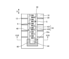
- stacking direction
- piezoelectric element
- Prior art date
- Legal status (The legal status is an assumption and is not a legal conclusion. Google has not performed a legal analysis and makes no representation as to the accuracy of the status listed.)
- Ceased
Links
Images









Classifications
-
- H—ELECTRICITY
- H10—SEMICONDUCTOR DEVICES; ELECTRIC SOLID-STATE DEVICES NOT OTHERWISE PROVIDED FOR
- H10N—ELECTRIC SOLID-STATE DEVICES NOT OTHERWISE PROVIDED FOR
- H10N30/00—Piezoelectric or electrostrictive devices
- H10N30/50—Piezoelectric or electrostrictive devices having a stacked or multilayer structure
-
- H—ELECTRICITY
- H10—SEMICONDUCTOR DEVICES; ELECTRIC SOLID-STATE DEVICES NOT OTHERWISE PROVIDED FOR
- H10N—ELECTRIC SOLID-STATE DEVICES NOT OTHERWISE PROVIDED FOR
- H10N30/00—Piezoelectric or electrostrictive devices
- H10N30/80—Constructional details
- H10N30/87—Electrodes or interconnections, e.g. leads or terminals
- H10N30/872—Interconnections, e.g. connection electrodes of multilayer piezoelectric or electrostrictive devices
-
- H—ELECTRICITY
- H10—SEMICONDUCTOR DEVICES; ELECTRIC SOLID-STATE DEVICES NOT OTHERWISE PROVIDED FOR
- H10N—ELECTRIC SOLID-STATE DEVICES NOT OTHERWISE PROVIDED FOR
- H10N30/00—Piezoelectric or electrostrictive devices
- H10N30/80—Constructional details
- H10N30/88—Mounts; Supports; Enclosures; Casings
- H10N30/883—Additional insulation means preventing electrical, physical or chemical damage, e.g. protective coatings
Definitions
- the disclosed embodiment relates to a piezoelectric element.
- a piezoelectric element that includes a laminate in which piezoelectric bodies and internal electrodes are stacked in multiple layers, a conductor layer located on the side of the laminate and connected to the internal electrodes, and an electrode plate whose width direction is partially joined to the conductor layer via a conductive bonding material (see, for example, Patent Document 1). Also proposed is a piezoelectric element structure in which the conductor layer and the electrode plate are covered by a covering layer located on the side of the laminate (see, for example, Patent Document 2).
- the piezoelectric element includes a laminate, a conductor layer, an electrode plate, and a covering layer.
- the laminate is a stack of multiple piezoelectric bodies and internal electrodes.
- the conductor layer is connected to the internal electrodes and is positioned along the stacking direction of the laminate.
- the electrode plate is bonded to the conductor layer via a conductive bonding material and is positioned along the stacking direction of the laminate.
- the covering layer covers the conductor layer and the electrode plate.
- the electrode plate has multiple slits that extend in a direction intersecting the stacking direction.
- the piezoelectric element has a first gap between the electrode plate, the conductor layer, and the bonding material.
- the possibility of peeling off of the electrode plate covered with the coating layer can be reduced.
- FIG. 1 is a perspective view showing the overall configuration of a piezoelectric element according to an embodiment.
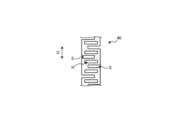
- FIG. 2 is an enlarged plan view showing an example of the configuration of an electrode plate and its surroundings according to the embodiment.
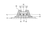
- FIG. 3 is a cross-sectional view taken along line III-III in FIG.
- FIG. 4 is a cross-sectional view taken along line IV-IV in FIG.
- FIG. 5 is a cross-sectional view showing an example of the configuration of an electrode plate and its surroundings according to the first alternative embodiment.
- FIG. 6 is a cross-sectional view showing an example of the configuration of an electrode plate and its surroundings according to the first alternative embodiment.
- FIG. 7 is a cross-sectional view showing an example of the configuration of an electrode plate and its surroundings according to another embodiment 2. In FIG. FIG. FIG.
- FIG. 8 is a cross-sectional view showing an example of the configuration of an electrode plate and its surroundings according to another embodiment 2.
- FIG. 9 is an enlarged plan view showing an example of the configuration of an electrode plate according to another embodiment 3.
- FIG. 10 is an enlarged plan view showing an example of the configuration of an electrode plate according to another embodiment 4.
- FIG. 11 is an enlarged plan view showing an example of the configuration of an electrode plate and its periphery according to another embodiment 5.
- FIG. 12 is a cross-sectional view taken along line XII-XII of FIG. 13 is a cross-sectional view taken along line XIII-XIII in FIG.
- FIG. 14 is a cross-sectional view showing an example of the configuration of an electrode plate and its surroundings according to another embodiment 6.
- FIG. 15 is a cross-sectional view showing an example of the configuration of an electrode plate and its surroundings according to another embodiment 6.
- FIG. 16 is an enlarged plan view showing an example of the configuration of an electrode plate and its periphery according to another embodiment 7.
- FIG. 17 is a cross-sectional view taken along line XVII-XVII of FIG.
- FIG. 18 is a cross-sectional view showing an example of the configuration of an electrode plate and its surroundings according to another embodiment 8.
- FIG. 19 is an enlarged plan view showing an example of the configuration of an electrode plate and its surroundings according to another embodiment 9.
- FIG. 19 is an enlarged plan view showing an example of the configuration of an electrode plate and its surroundings according to another embodiment 9.
- FIG. 20 is a cross-sectional view taken along line XX-XX of FIG. 19.
- FIG. FIG. 21 is a cross-sectional view showing an example of the configuration of an electrode plate and its surroundings according to another embodiment 10.
- FIG. 22 is an enlarged plan view showing an example of the configuration of an electrode plate and its surroundings according to another embodiment 11.
- FIG. 23 is a cross-sectional view showing an example of the configuration of an electrode plate and its surroundings according to another embodiment 12. As shown in FIG.
- Fig. 1 is a perspective view showing the overall configuration of a piezoelectric element 1 according to an embodiment.
- the piezoelectric element 1 includes a laminate 10, a pair of conductor layers 20, a pair of electrode plates 40, and a covering layer 50 (see FIGS. 3 and 4).
- the pair of conductor layers 20 include conductor layer 20A and conductor layer 20B
- the pair of electrode plates 40 include electrode plate 40A and electrode plate 40B.
- the covering layer 50, conductor layer 20B, and electrode plate 40B are omitted from FIG. 1.
- the laminate 10 has a columnar shape.
- the laminate 10 is, for example, a square prism (rectangular parallelepiped) with a length of 0.5 (mm) to 10 (mm), a width of 0.5 (mm) to 10 (mm), and a height of 1 (mm) to 100 (mm).
- the shape of the laminate 10 is not limited to a square prism, and may be a hexagonal prism, an octagonal prism, a cylinder, or the like.
- the laminate 10 has a piezoelectric body 11, an internal electrode 12, and a planned fracture layer 13.
- the laminate 10 is constructed by stacking the piezoelectric body 11, the internal electrode 12, and the planned fracture layer 13 in a predetermined order along the stacking direction D.
- the stacking direction D of the laminate 10 coincides with the longitudinal direction of the laminate 10.
- the piezoelectric body 11 is made of a piezoelectric material having piezoelectric properties, such as piezoelectric ceramics, for example, a perovskite oxide made of lead zirconate titanate ( PbZrO3 - PbTiO3 ), lithium niobate ( LiNbO3 ), or lithium tantalate ( LiTaO3 ).
- a piezoelectric material having piezoelectric properties such as piezoelectric ceramics, for example, a perovskite oxide made of lead zirconate titanate ( PbZrO3 - PbTiO3 ), lithium niobate ( LiNbO3 ), or lithium tantalate ( LiTaO3 ).
- the average particle size of such piezoelectric ceramics is, for example, 1.6 ( ⁇ m) to 2.8 ( ⁇ m).
- the thickness of the piezoelectric body 11 is, for example, 3 ( ⁇ m) to 250 ( ⁇ m).
- the internal electrode 12 is made of a conductive material and includes a plurality of first electrodes 12a and a plurality of second electrodes 12b.
- the first electrodes 12a are electrically connected to a conductor layer 20A disposed on one side surface 10a of the laminate 10.
- a predetermined positive voltage is applied to the first electrodes 12a via the conductor layer 20A.
- the second electrode 12b is electrically connected to a conductor layer 20B disposed on the side surface 10b opposite the side surface 10a of the laminate 10.
- a predetermined negative voltage (or ground voltage) is applied to the second electrode 12b via the conductor layer 20B.
- the first electrode 12a, the second electrode 12b, and the piezoelectric body 11 are laminated so that the piezoelectric body 11 is disposed between the first electrode 12a and the second electrode 12b. This allows the laminate 10 to apply a drive voltage to the piezoelectric body 11 by the first electrode 12a and the second electrode 12b.
- the laminate 10 according to the embodiment is composed of an active section formed by alternately stacking multiple piezoelectric bodies 11 and internal electrodes 12, and an inactive section having a piezoelectric body 11 and arranged on both ends of the active section in the stacking direction D.
- the active portion is a portion that expands or contracts (hereinafter also referred to as expanding or contracting) in the stacking direction D when a drive voltage is applied to the laminate 10 from the outside.
- the inactive portion is a portion that does not expand or contract even when a drive voltage is applied to the laminate 10 from the outside.
- the lower end in FIG. 1 is referred to as the base end 10e of the laminate 10
- the upper end in FIG. 1 is referred to as the tip end 10f of the laminate 10.
- the base end 10e of the laminate 10 is fixed, and the tip end 10f of the laminate 10 is displaced along the stacking direction D.
- the material of the internal electrode 12 is, for example, a metal whose main component is silver, silver-palladium, silver-platinum, or copper.
- the internal electrode 12 can be formed, for example, by co-firing with the piezoelectric body 11.
- the thickness of the internal electrode 12 is, for example, 0.1 ( ⁇ m) to 5 ( ⁇ m).
- the planned rupture layer 13 is a layer for relieving stress caused by driving the laminate 10.
- Examples of the planned rupture layer 13 include a porous metal layer that does not function as an internal electrode 12, or a metal layer that has cracks in it. Note that the planned rupture layer 13 may be omitted in the laminate 10 according to the embodiment.
- the pair of conductor layers 20 includes conductor layer 20A located on side surface 10a of laminate 10 and conductor layer 20B located on side surface 10b of laminate 10. Conductor layer 20 is disposed across the entire active portion of laminate 10. Conductor layer 20 is positioned along stacking direction D.
- the material of the conductor layer 20 is, for example, a metal whose main component is silver or copper.
- the conductor layer 20 can be, for example, a metallized layer made of a sintered body of the above-mentioned metal and glass.
- the thickness of the conductor layer 20 is, for example, 5 ( ⁇ m) to 500 ( ⁇ m).
- the pair of electrode plates 40 includes electrode plate 40A and electrode plate 40B, which are electrically connected to the pair of conductor layers 20, respectively. Specifically, electrode plate 40A is electrically connected to conductor layer 20A, and electrode plate 40B is electrically connected to conductor layer 20B.
- the electrode plate 40 is positioned along the stacking direction D of the laminate 10. A portion of the electrode plate 40 in the width direction intersecting with the stacking direction D is joined to the conductor layer 20 via a conductive bonding material 30.
- bonding material 30 for example, an epoxy resin or polyimide resin containing a metal powder with high conductivity, such as Ag powder or Cu powder, is used.
- the material of the electrode plate 40 is, for example, a metal such as copper, iron, stainless steel, or phosphor bronze.
- the width of the electrode plate 40 is, for example, 0.5 (mm) to 10 (mm), and the thickness of the electrode plate 40 is, for example, 0.01 (mm) to 1.0 (mm).
- the surface of the electrode plate 40 may be provided with a plating film such as tin plating or silver plating to improve electrical conductivity and thermal conductivity.
- the coating layer 50 is positioned around the entire side of the laminate 10, including side 10a and side 10b, and covers the conductor layer 20 and the electrode plate 40. By arranging the coating layer 50 on the sides 10a and 10b, it is possible to reduce creeping discharge between the two electrodes that occurs when a high voltage is applied during operation.
- the coating layer 50 is made of, for example, an insulator.
- insulators that can be used for the coating layer 50 include fluorine-based resin, silicone resin, epoxy resin, and nylon resin.
- the covering layer 50 only needs to be located on at least the side surfaces 10a and 10b of the laminate 10 so as to cover the conductor layer 20 and the electrode plate 40, and does not necessarily have to be arranged around the entire side surface.
- the covering layer 50 may not be arranged on the side surfaces 10c and 10d of the laminate 10, but only on the side surfaces 10a and 10b.
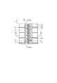
- Fig. 2 is an enlarged plan view showing an example of the configuration of the electrode plate 40 and its periphery according to the embodiment.
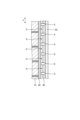
- Fig. 3 is a cross-sectional view taken along line III-III in Fig. 2.
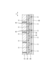
- Fig. 4 is a cross-sectional view taken along line IV-IV in Fig. 2.
- the covering layer 50 is omitted in Fig. 2.
- the electrode plate 40 is a plate-shaped member that extends in the stacking direction D of the laminate 10, and a portion of the width direction that intersects with the stacking direction D is joined to the conductor layer 20 via a conductive bonding material 30.
- the electrode plate 40 has a plurality of slits S.
- the slits S are cut out to extend, for example, along the width direction of the electrode plate 40 (i.e., the direction intersecting with the stacking direction D).
- the multiple slits S are cut out alternately from the end faces of both ends located outside the bonding material 30 in the width direction of the electrode plate 40 in a planar view, and are arranged side by side at approximately equal intervals along the stacking direction D.
- the multiple slits S all have approximately the same length.
- the length of the slits S refers to the length in the cutout direction of the slits S (i.e., the width direction of the electrode plate 40).
- the lengths of the multiple slits S are set so that the tips overlap when viewed in the stacking direction D.
- overlapping means that adjacent slits S have areas that face each other when viewed in the stacking direction D.
- the electrode plate 40 can expand and contract in the stacking direction D in accordance with the expansion and contraction of the laminate 10 in the stacking direction D. Therefore, according to the embodiment, the possibility of the electrode plate 40 peeling off from the laminate 10 or the conductor layer 20 can be reduced.
- the electrode plate 40 is covered together with the conductor layer 20 by a covering layer 50 (see Figures 3 and 4) located on the side of the laminate 10.
- the electrode plate 40 and the conductor layer 20 are completely covered with the covering layer 50, when the laminate 10 expands and contracts, a large stress that limits the deformation of the electrode plate 40 is generated in the electrode plate 40.
- the stress that limits the torsional deformation is concentrated on the end portion of the electrode plate 40 that is located outside the bonding material 30 in the width direction in a planar view. Then, as the stress that limits the deformation is generated in the electrode plate 40 in response to the expansion and contraction of the laminate 10, there is a possibility that the electrode plate 40 will peel off from the laminate 10 or the conductor layer 20.
- the conductor layer 20 and the electrode plate 40 are covered with a covering layer 50 while leaving a gap G between the conductor layer 20 and the end portion of the electrode plate 40 located outside the bonding material 30 in a planar view.
- the piezoelectric element 1 has a gap G between the electrode plate 40, the conductor layer 20, and the bonding material 30.
- a plurality of such gaps G are formed at positions that do not overlap with the plurality of slits S of the electrode plate 40 in a planar view (see Fig. 2).
- the end portion of the electrode plate 40 located outside the bonding material 30 in a planar view and the conductor layer 20 are positioned opposite each other with each gap G therebetween.
- the gap G is an example of a first gap.
- the stress generated in the electrode plate 40 due to the expansion and contraction of the laminate 10 can be alleviated, thereby reducing the possibility of the electrode plate 40 peeling off from the laminate 10 or the conductor layer 20.
- the gap G between one end of the electrode plate 40 located outside the bonding material 30 in a plan view and the conductor layer 20 is separated from the gap G between the other end of the electrode plate 40 and the conductor layer 20. That is, the gap G between one end of the electrode plate 40 and the conductor layer 20 and the gap G between the other end of the electrode plate 40 and the conductor layer 20 are not connected, and are individually closed with the bonding material 30 as a boundary.
- the stress generated in the electrode plate 40 due to the expansion and contraction of the laminate 10 can be further alleviated, and the possibility of the electrode plate 40 peeling off from the laminate 10 or the conductor layer 20 can be further reduced.
- the gap G between one end of the electrode plate 40 and the conductor layer 20 and the gap G between the other end of the electrode plate 40 and the conductor layer 20 are positioned at positions offset from each other in the stacking direction D of the laminate 10. This makes it easier for twisting deformation to occur at both ends in the width direction of the electrode plate 40 in accordance with the expansion and contraction of the laminate 10 in the stacking direction D. Therefore, according to the embodiment, the stress generated in the electrode plate 40 due to the expansion and contraction of the laminate 10 can be further alleviated, thereby further reducing the possibility of the electrode plate 40 peeling off from the laminate 10 or the conductor layer 20.
- the bonding material 30 may be positioned so as to overlap the center portion of the electrode plate 40 in a plan view. This allows the gap G on one end side of the electrode plate 40 divided by the bonding material 30 and the gap G on the other end side to be approximately the same size, and torsional deformation occurs evenly at both ends in the width direction of the electrode plate 40 in accordance with the expansion and contraction of the laminate 10 in the stacking direction D. Therefore, according to the embodiment, the stress generated in the electrode plate 40 due to the expansion and contraction of the laminate 10 can be evenly alleviated at both ends in the width direction of the electrode plate 40, thereby further reducing the possibility of the electrode plate 40 peeling off from the laminate 10 or the conductor layer 20.
- the bonding material 30 may have an area that overlaps with the slit S of the electrode plate 40 in a plan view. This makes it difficult for the electrode plate 40 to peel off from the bonding material 30 near the slit S of the electrode plate 40.
- the length of the slit S in the electrode plate 40 is greater than half the width of the electrode plate 40.
- the position of the tip of the slit S in the cutout direction which is the starting point of the twist that occurs at the end in the width direction of the electrode plate 40, is misaligned with the position of the bonding material 30 located in the center part of the electrode plate 40, making it difficult for the electrode plate 40 to peel off from the bonding material 30.
- FIGS. 5 and 6 are cross-sectional views showing an example of the configuration of the electrode plate 40 and its surroundings according to another embodiment 1.
- FIG. 5 corresponds to a cross-sectional view taken along line III-III in FIG. 2
- FIG. 6 corresponds to a cross-sectional view taken along line IV-IV in FIG. 2.
- the configuration of the covering layer 50 differs from the above-described embodiment.
- the covering layer 50 has a protruding portion 51.
- the protruding portion 51 is positioned protruding inward from the end of the electrode plate 40 in the direction intersecting the stacking direction D (i.e., the width direction) and is in contact with the conductor layer 20.
- the inward side means the side toward the center of the electrode plate 40.
- the protruding portion 51 is an example of a first protruding portion.
- the adhesion between the covering layer 50 and the conductor layer 20 is improved compared to when the protrusion 51 is not provided, and therefore the adhesion between the electrode plate 40 covered by the covering layer 50 and the conductor layer 20 is improved. Therefore, according to other embodiment 1, it is possible to reduce the possibility that the electrode plate 40 covered by the covering layer 50 will peel off from the conductor layer 20.
- the covering layer 50 may have a protruding portion 52.
- the protruding portion 52 is located protruding inward from the inner wall surface of the slit S in the electrode plate 40 and is in contact with the conductor layer 20.
- the inner side means the side closer to the center of each electrode plate.
- the protruding portion 52 is an example of a second protruding portion.
- the adhesion between the coating layer 50 and the conductor layer 20 is improved compared to when the protrusion 52 is not provided, and therefore the adhesion between the electrode plate 40 covered by the coating layer 50 and the conductor layer 20 is improved. Therefore, according to the alternative embodiment 1, it is possible to reduce the possibility that the electrode plate 40 covered by the coating layer 50 will peel off from the conductor layer 20.
- ⁇ Another embodiment 2> 7 and 8 are cross-sectional views showing an example of the configuration of the electrode plate 40 and its surroundings according to another embodiment 2.
- Fig. 7 corresponds to a cross-sectional view taken along line III-III in Fig. 2
- Fig. 8 corresponds to a cross-sectional view taken along line IV-IV in Fig. 2.
- the configuration of the electrode plate 40 differs from that of the alternative embodiment 2 described above.
- the electrode plate 40 has a protrusion 41 that protrudes in the thickness direction of the electrode plate 40 on the periphery of the end of the electrode plate 40 in the direction intersecting with the stacking direction D (i.e., the width direction).
- the protrusion 41 is an example of a first protrusion.
- the strength of both ends of the electrode plate 40 is increased compared to a case in which the protrusion 41 is not provided, and therefore damage to both ends of the electrode plate 40 due to repeated deformation is less likely to occur. Therefore, according to other embodiment 2, the durability of the electrode plate 40 can be improved. Note that, although the protrusion 41 is located on the laminate 10 side and on the opposite side of the laminate 10 in FIG. 7, it may be located only on the laminate 10 side.
- the thickness of the protruding portion 51 of the coating layer 50 located near the protruding portion 41 is reduced by the thickness of the protruding portion 41, so that the electrode plate 40 can be easily deformed in accordance with the expansion and contraction of the laminate 10 in the stacking direction D. Therefore, according to alternative embodiment 2, the stress generated in the electrode plate 40 due to the expansion and contraction of the laminate 10 can be further alleviated, so that the possibility of the electrode plate 40 peeling off from the laminate 10 or the conductor layer 20 can be further reduced.
- the protrusions 41 may extend along the stacking direction D of the laminate 10. This further increases the strength of both ends of the electrode plate 40, making it less likely that damage to both ends of the electrode plate 40 will occur due to repeated deformation. Therefore, according to alternative embodiment 2, the durability of the electrode plate 40 can be further improved.
- the electrode plate 40 may have a protrusion 42 that protrudes in the thickness direction of the electrode plate 40 on the periphery of the slit S in the electrode plate 40.
- the protrusion 42 is an example of a second protrusion.
- the strength of the periphery of the slits S in the electrode plate 40 is increased compared to when the protrusions 42 are not provided, and therefore the periphery of the slits S in the electrode plate 40 is less likely to be damaged due to repeated deformation. Therefore, according to the second alternative embodiment, the durability of the electrode plate 40 can be improved. Note that, although the protrusions 42 are located on the laminate 10 side and the opposite side of the laminate 10 in FIG. 8, they may be located only on the laminate 10 side.
- the thickness of the protruding portion 52 of the coating layer 50 located near the protruding portion 42 is reduced by the thickness of the protruding portion 42, making it easier to deform the electrode plate 40 in accordance with the expansion and contraction of the laminate 10 in the stacking direction D. Therefore, according to alternative embodiment 2, the stress generated in the electrode plate 40 due to the expansion and contraction of the laminate 10 can be further alleviated, thereby further reducing the possibility of the electrode plate 40 peeling off from the laminate 10 or the conductor layer 20.
- the protrusions 42 may extend along the longitudinal direction of the slits S. This further increases the strength of the edges of the slits S in the electrode plate 40, making it less likely that damage to the edges of the slits S in the electrode plate 40 will occur due to repeated deformation. Therefore, according to alternative embodiment 2, the durability of the electrode plate 40 can be further improved.
- the protrusions 41 and 42 can be formed by etching the side of the metal plate 40a (see FIG. 7), which serves as the base material for the electrode plate 40, to form a recess, and then plating the corners located on the periphery of the recess more thickly than the other parts.
- Fig. 9 is an enlarged plan view showing an example of the configuration of the electrode plate 40 according to Alternative Embodiment 3.
- the shape of the electrode plate 40 is different from that of the above-described embodiments.
- the electrode plate 40 has a plurality of slits S and a plurality of through holes H.
- the slits S are formed, for example, so as to extend along the width direction of the electrode plate 40 (i.e., the direction intersecting with the stacking direction D) to the end face of one of the ends of the electrode plate 40. Furthermore, the through holes H are formed so as to extend along the same direction as the slits S, but do not extend to the end faces of either end of the electrode plate 40.
- the multiple slits S are cut alternately from the end faces of both ends of the electrode plate 40 in the width direction, and are arranged side by side at approximately equal intervals along the stacking direction D.
- the multiple slits S all have approximately the same length.
- the lengths of the multiple slits S are set so that the tips overlap when viewed in the stacking direction D.
- the electrode plate 40 by arranging multiple slits S in the electrode plate 40, the electrode plate 40 can expand and contract in the stacking direction D in accordance with the expansion and contraction of the laminate 10 in the stacking direction D. Therefore, according to the other embodiment 3, the possibility of the electrode plate 40 peeling off from the laminate 10 or the conductor layer 20 can be reduced.
- through holes H are located between slits S that are alternately cut out from the end faces of both ends in the width direction of the electrode plate 40.
- Such through holes H are arranged at equal intervals with respect to both adjacent slits S, and have a length approximately equal to the length of the slits S.
- a slit S extending from the end face of one end, a through hole H, and a slit S and a through hole H extending from the end face of the other end are arranged in this order at approximately equal intervals along the stacking direction D.
- a through hole H is disposed at a location where the tips of a slit S extending from the end face of one end and a slit S extending from the end face of the other end overlap.
- the possibility of the electrode plate 40 peeling off from the laminate 10 or the conductor layer 20 can be further reduced.
- Fig. 10 is an enlarged plan view showing an example of the configuration of an electrode plate 40 according to Alternative Embodiment 4.
- Alternative Embodiment 4 shown in Fig. 10 the arrangement of the through holes H is different from that of Alternative Embodiment 3 described above.
- two or more through holes H are located adjacent to each other between slits S cut alternately from the end faces of both ends in the width direction of the electrode plate 40.
- a slit S extending from an end face at one end, a through hole H, a through hole H, and a slit S extending from an end face at the other end are arranged in this order at approximately equal intervals along the stacking direction D.
- the stress generated in the electrode plate 40 due to the expansion and contraction of the laminate 10 can be further alleviated. Therefore, according to the fourth alternative embodiment, the possibility of the electrode plate 40 peeling off from the laminate 10 or the conductor layer 20 can be further reduced.
- Fig. 11 is an enlarged plan view showing an example of the configuration of an electrode plate 40 and its periphery according to another embodiment 5.
- Fig. 12 is a cross-sectional view taken along line XII-XII in Fig. 11.
- Fig. 13 is a cross-sectional view taken along line XIII-XIII in Fig. 11.
- the coating layer 50 is omitted from Figs. 11 to 13.
- the fifth alternative embodiment shown in Figures 11 to 13 differs from the above-mentioned embodiments in the configuration of the electrode plate 40 and in the fact that a fixing material 60 is newly provided.
- the electrode plate 40 is a plate-shaped member extending in the stacking direction D of the laminate 10, and has a main body portion 43 joined to the conductor layer 20 via a conductive bonding material 30, and a protruding portion 44 that protrudes from one end 43a of the main body portion 43 in the stacking direction D and faces the laminate 10.
- the main body 43 has a first portion 431 that contacts the bonding material 30, and a second portion 432 that is located on both sides of the first portion 431 in the width direction (i.e., the direction intersecting the stacking direction D) and faces the conductor layer 20 without contacting the bonding material 30.
- the main body 43 of the electrode plate 40 has multiple slits S.
- the slits S are cut out to extend, for example, along the width direction of the main body 43 (i.e., the direction intersecting with the stacking direction D).
- the multiple slits S are cut alternately from both sides of the main body 43 (i.e., the sides of the pair of second portions 432) and are arranged side by side at approximately equal intervals along the stacking direction D.
- the multiple slits S all have approximately the same length.
- the length of the slits S refers to the length in the cutout direction of the slits S (i.e., the width direction of the main body 43).
- the lengths of the multiple slits S are set so that the tips overlap when viewed in the stacking direction D.
- overlapping means that adjacent slits S have areas that face each other when viewed in the stacking direction D.
- the main body 43 of the electrode plate 40 by arranging multiple slits S in the main body 43 of the electrode plate 40, the main body 43 can expand and contract in the stacking direction D in accordance with the expansion and contraction of the laminate 10 in the stacking direction D. Therefore, according to the other embodiment 5, the possibility of the electrode plate 40 peeling off from the laminate 10 or the conductor layer 20 can be reduced.
- the protruding portion 44 of the electrode plate 40 faces the laminate 10 across a first gap G1 .
- the piezoelectric element 1 includes a fixing material 60.
- the fixing material 60 fixes the electrode plate 40 and the laminate 10.
- the fixing material 60 fixes at least the protruding portion 44 of the electrode plate 40 to the laminate 10.
- the fixing material 60 according to alternative embodiment 5 does not necessarily have to fix the entire periphery of the protruding portion 44 to the laminate 10. In short, it is sufficient that the fixing material 60 fixes at least a portion of the periphery of the protruding portion 44 to the laminate 10.
- the fixing material 60 according to the fifth alternative embodiment may be fixed to the laminate 10 along the entire periphery of the protruding portion 44, with a predetermined area surrounded by the periphery of the protruding portion 44 remaining on the protruding portion 44. This allows the predetermined area remaining on the protruding portion 44 to be used as an area for joining a lead terminal that supplies power to the electrode plate 40.
- the fixing material 60 is made of, for example, an insulating material that is heat resistant and flexible.
- an insulating material that is heat resistant and flexible.
- epoxy resin, glass, ceramics, or a composite material of epoxy resin and ceramics is used as the insulating material for the fixing material 60.
- the ceramic material may be the same as the piezoelectric ceramic that becomes the piezoelectric body 11.
- the fixing material 60 fixes at least the protruding portion 44 of the electrode plate 40 to the laminate 10 in a state in which the first gap G1 is maintained between the protruding portion 44 and the laminate 10.
- the piezoelectric element 1 has the first gap G1 between the fixing material 60, the protruding portion 44, and the laminate 10.
- the protruding portion 44 on the first gap G1 expands and contracts along the stacking direction D, and the stress generated at the end portion (near one end 43a) of the joint portion between the electrode plate 40 and the conductor layer 20 can be released to the interface between the fixing material 60 and the laminate 10. Therefore, according to the fifth alternative embodiment, the stress generated at the end portion (near one end 43a) of the joint portion between the electrode plate 40 and the conductor layer 20 due to the expansion and contraction of the laminate 10 in the stacking direction D can be dispersed, and the possibility of the electrode plate 40 peeling off from the conductor layer 20 can be reduced.
- Figures 14 and 15 are cross-sectional views showing an example of the configuration of the electrode plate 40 and its surroundings according to another embodiment 6.
- Figure 14 corresponds to a cross-sectional view taken along line XII-XII in Figure 11
- Figure 15 corresponds to a cross-sectional view taken along line XIII-XIII in Figure 11. Note that, for convenience of explanation, the coating layer 50 is omitted in Figures 14 and 15.
- the configuration of the fixing material 60 differs from Alternative Embodiment 5 described above.
- the fixing material 60 has a protruding portion 61.
- the protruding portion 61 is located protruding inward from the periphery of the protruding portion 44 and is in contact with the laminate 10.
- “inward from the periphery of the protruding portion 44” can also be rephrased as a direction approaching the central axis of the protruding portion 44 (electrode plate 40).
- the protruding portion 61 is an example of a first protruding portion.
- the stress generated at the end (near one end 43a) of the joint between the electrode plate 40 and the conductor layer 20 can be efficiently released from the interface between the fixing material 60 and the laminate 10 in accordance with the expansion and contraction of the laminate 10 in the stacking direction D. Therefore, according to another embodiment 6, the stress generated at the end of the joint between the electrode plate 40 and the conductor layer 20 due to the expansion and contraction of the laminate 10 in the stacking direction D can be more efficiently dispersed, and the possibility of the electrode plate 40 peeling off from the conductor layer 20 can be further reduced.
- Fig. 16 is an enlarged plan view showing an example of the configuration of the electrode plate 40 and its periphery according to Alternative Embodiment 7.
- Fig. 17 is a cross-sectional view taken along line XVII-XVII shown in Fig. 16 .
- the fixing material 60 fixes the main body 43 and the conductor layer 20 to the laminate 10 at one end of the conductor layer 20 located on the one end 43a side of the main body 43.
- the stress generated at the end (near one end 43a) of the joint between the electrode plate 40 and the conductor layer 20 can be efficiently released by the interface between the fixing material 60 and the laminate 10 in accordance with the expansion and contraction of the laminate 10 in the stacking direction D. Therefore, according to other embodiment 7, the stress generated at the end of the joint between the electrode plate 40 and the conductor layer 20 due to the expansion and contraction of the laminate 10 in the stacking direction D can be more efficiently dispersed, and the possibility of the electrode plate 40 peeling off from the conductor layer 20 can be further reduced.
- ⁇ Other embodiment 8> 18 is a cross-sectional view showing an example of the configuration of an electrode plate 40 and its surroundings according to another embodiment 8.
- Fig. 18 corresponds to a cross-sectional view taken along line XVII-XVII shown in Fig. 16 .
- the main body 43 has the first portion 431 in contact with the bonding material 30, and the second portions 432 located on both sides of the first portion 431 in the width direction (i.e., the direction intersecting the stacking direction D) and facing the conductor layer 20 without contacting the bonding material 30.
- the second portions 432 face the conductor layer 20 across the second gap G2 .
- the configuration of the fixing material 60 differs from alternative embodiment 7 described above.
- the fixing material 60 has a protruding portion 62.
- the protruding portion 62 is positioned protruding inward from the side of the second portion 432 and is in contact with the conductor layer 20.
- the "inward from the side of the second portion 432" can also be rephrased as the direction approaching the central axis of the protrusion 44 (electrode plate 40).
- the protruding portion 62 is an example of a second protruding portion.
- the adhesion between the fixing material 60 and the conductor layer 20 is improved compared to when the protrusion 62 is not provided, and therefore the adhesion between the fixing material 60 and the laminate 10 is improved. Therefore, according to another embodiment 8, the possibility that the conductor layer 20 will peel off from the laminate 10 can be reduced.
- Fig. 19 is an enlarged plan view showing an example of the configuration of an electrode plate 40 and its surroundings according to Alternative Embodiment 9.
- Fig. 20 is a cross-sectional view taken along line XX-XX shown in Fig. 19 .
- a coating layer 50 that covers the main body portion 43 and the conductor layer 20 is located on a side surface 10a (an example of a surface that is located along the stacking direction D of the laminate 10) of the laminate 10.
- a coating layer 50 that covers the main body portion 43 and the conductor layer 20 is also located on a side surface 10b (an example of a surface that is located along the stacking direction D of the laminate 10) of the laminate 10.
- the coating layer 50 is made of, for example, an insulator.
- insulators that can be used for the coating layer 50 include fluorine-based resin, silicone resin, epoxy resin, and nylon resin.
- the end of the covering layer 50 covers the end of the fixing material 60 located on one end 43a side of the main body 43.
- the stress generated at the end (near one end 43a) of the joint between the electrode plate 40 and the conductor layer 20 can be released to the interface between the fixing material 60 and the laminate 10 and the interface between the coating layer 50 and the laminate 10 in accordance with the expansion and contraction of the laminate 10 in the stacking direction D. Therefore, according to other embodiment 9, the stress generated at the end of the joint between the electrode plate 40 and the conductor layer 20 due to the expansion and contraction of the laminate 10 in the stacking direction D can be more efficiently dispersed, and the possibility of the electrode plate 40 peeling off from the conductor layer 20 can be further reduced.
- ⁇ Other embodiment 10> 21 is a cross-sectional view showing an example of the configuration of an electrode plate 40 and its surroundings according to another embodiment 10.
- Fig. 21 corresponds to a cross-sectional view taken along line XXI-XXI shown in Fig. 19 .
- the configuration of the coating layer 50 differs from that of the other embodiment 9 described above.
- the coating layer 50 is located around the entire periphery of the side surfaces, including the side surface 10a, of the laminate 10. That is, the coating layer 50 is located not only on the side surfaces 10a and 10b of the laminate 10, but also on the side surfaces 10c (see FIG. 1) and 10d (see FIG. 1) that are located between the side surfaces 10a and 10b.
- the stress generated in the coating layer 50 can be dispersed around the entire side surface of the laminate 10 in response to the expansion and contraction of the laminate 10 in the stacking direction D.
- ⁇ Other embodiment 11> 22 is an enlarged plan view showing an example of the configuration of the electrode plate 40 and its surroundings according to another embodiment 11.
- the laminate 10 is composed of an active portion 10A formed by alternately laminating a plurality of piezoelectric bodies 11 and internal electrodes 12, and an inactive portion 10B disposed on both ends of the active portion in the lamination direction D, which has the piezoelectric body 11 but does not have the internal electrode 12.
- the electrode plate 40 has a wide portion 45 that is wider than the other portions at least in the protruding portion 44 at a position that overlaps with the inactive portion 10B in a plan view.
- the fixing material 60 may fix the wide portion 45 to the laminate 10.
- the stress generated at the end (near one end 43a) of the joint between the electrode plate 40 and the conductor layer 20 can be efficiently released by the interface between the fixing material 60 and the laminate 10 in accordance with the expansion and contraction of the laminate 10 in the stacking direction D. Therefore, according to other embodiment 11, the stress generated at the end of the joint between the electrode plate 40 and the conductor layer 20 due to the expansion and contraction of the laminate 10 in the stacking direction D can be more efficiently dispersed, and the possibility of the electrode plate 40 peeling off from the conductor layer 20 can be further reduced.
- ⁇ Other embodiment 12> 23 is a cross-sectional view showing an example of the configuration of an electrode plate 40 and its surroundings according to another embodiment 12.
- Fig. 23 corresponds to a cross-sectional view taken along line XXI-XXI shown in Fig. 19.
- the protrusion 44 is inclined so that the distance between the protrusion 44 and the laminate 10 narrows toward the tip 44a of the protrusion 44. In other words, the protrusion 44 is inclined downward toward the tip 44a of the protrusion 44.
- a portion of the uncured fixing material 60 is appropriately filled into the gap between the tip 44a of the protrusion 44 and the laminate 10, thereby improving the adhesion strength between the tip 44a of the protrusion 44 and the laminate 10 after the fixing material 60 has hardened.
- the shape of the through hole H is rectangular in a plan view, but it may be rounded near the end in the width direction of the electrode plate 40. In this case, it is possible to reduce the risk of stress concentrating on the corners and causing cracks during expansion and contraction.
- a ceramic green sheet that will become the piezoelectric layer (piezoelectric body 11) is prepared. Specifically, a calcined powder of piezoelectric ceramics, a binder having an organic polymer such as an acrylic or butyral-based polymer, and a plasticizer are mixed to prepare a ceramic slurry. Then, a ceramic green sheet is prepared from this ceramic slurry by using a tape molding method such as a well-known doctor blade method or a calendar roll method.
- any material having piezoelectric properties may be used, and for example, a perovskite oxide having PbZrO 3 -PbTiO 3 may be used.
- a plasticizer dibutyl phthalate (DBP), dioctyl phthalate (DOP), etc. may be used.
- a conductive paste that will become the internal electrodes 12 is prepared. Specifically, a binder and a plasticizer are added to and mixed with a silver-palladium alloy metal powder to prepare the conductive paste. This conductive paste is printed on the ceramic green sheets using a screen printing method. Next, multiple ceramic green sheets with the conductive paste printed on them are stacked together, and multiple ceramic green sheets with no conductive paste printed on both ends in the stacking direction are stacked together to obtain a laminated molded body. This laminated molded body is subjected to a binder removal process at a predetermined temperature, and then fired at 900 to 1200°C to obtain the laminated body 10.
- a conductive paste made of silver and glass is applied to the side of the laminate 10 and baked to form the conductor layer 20.
- the conductive paste is made by adding and mixing a binder, plasticizer, glass powder, etc. to a metal powder made mainly of silver, and the conductive layer 20 can be formed by printing it on the side of the laminate 10 by a method such as screen printing and baking it at 600 to 800°C.
- the bonding material 30 is applied to the upper surface of the conductor layer 20, and the electrode plate 40 is attached on top of it.
- the bonding material 30 is then dried at a temperature of 100 to 140°C, and then hardened at a temperature of 180 to 220°C to fix the electrode plate 40 in place.
- the coating layer 50 is applied to the laminate 10 by a general application method such as dipping, and after a degassing process, the coating layer 50 is cured.
- a general application method such as dipping
- the coating layer 50 is cured.
- minute voids of 0.1 ⁇ m or less may be dispersed within the coating layer 50, no voids G are formed. Therefore, voids G can also be formed by using a highly viscous resin as the coating layer 50 and applying it to a specified position by screen printing. Note that voids G can also be formed, for example, by the following method as another method.
- a photosensitive coating layer 50 is applied to the laminate 10.
- a gap G is then provided between the electrode plate 40 and the conductor layer 20, and the coating layer 50 is irradiated with light to harden it before it flows into the gap G.
- the coating layer 50 is applied twice. Specifically, the coating layer 50 is applied before the bonding material 30 and the electrode plate 40 are fixed. After that, plasma etching or blasting is performed on the area where the electrode plate 40 is to be fixed to expose the conductor layer 20, the bonding material 30 and the electrode plate 40 are fixed, and the coating layer 50 is applied again on the electrode plate 40 to form the gap G.
- the electrode plate 40 having the convex portions 41 (42) shown in Figures 7 and 8 is fixed to the laminate 10, the gap between the convex portions 41 (42) and the conductor layer 20 is reduced, and the coating layer 50 is applied by screen printing. This makes it difficult for the coating layer 50 to flow into the convex portions 41 (42), and in this state, the coating layer 50 is hardened to form a gap G.
- the piezoelectric element 1 of this example is produced.
- the piezoelectric element (e.g., piezoelectric element 1) according to the embodiment includes a laminate (e.g., laminate 10), a conductor layer (e.g., conductor layer 20), an electrode plate (e.g., electrode plate 40), and a covering layer (e.g., covering layer 50).
- the laminate includes a plurality of piezoelectric bodies (e.g., piezoelectric body 11) and internal electrodes (e.g., internal electrodes 12) stacked on top of each other.
- the conductor layer is connected to the internal electrodes and is located along the stacking direction (e.g., stacking direction D) of the laminate.
- the electrode plate is bonded to the conductor layer via a conductive bonding material (e.g., bonding material 30) and is located along the stacking direction of the laminate.
- the covering layer covers the conductor layer and the electrode plate.
- the electrode plate has a plurality of slits (e.g., slits S) extending in a direction (e.g., width direction) intersecting the stacking direction.
- the piezoelectric element has a first gap (e.g., gap G) between the electrode plate, the conductor layer, and the bonding material. This can reduce the possibility of peeling off of the electrode plate covered with the covering layer.
- (Appendix 1) a laminate in which a plurality of piezoelectric bodies and internal electrodes are laminated; a conductor layer connected to the internal electrode and positioned along a lamination direction of the laminate; an electrode plate joined to the conductor layer via a conductive bonding material and positioned along the stacking direction of the laminate; a covering layer that covers the conductor layer and the electrode plate; Equipped with The electrode plate has a plurality of slits extending in a direction intersecting the stacking direction, A piezoelectric element having a first gap between the electrode plate, the conductor layer, and the bonding material.
- (Appendix 2) The piezoelectric element of claim 1, wherein the covering layer has a first protruding portion that is positioned protruding inward from an end of the electrode plate in a direction intersecting the stacking direction and that contacts the conductor layer.
- Appendix 8 A piezoelectric element as described in any one of Appendices 1 to 7, wherein a gap between one end of the electrode plate located outside the bonding material in a planar view in the width direction and the conductor layer and a gap between the other end of the electrode plate and the conductor layer are separated.
- Piezoelectric element 10 Laminated body 10a to 10d Side 10e Base end 10f Tip 11 Piezoelectric body 12 Internal electrode 12a First electrode 12b Second electrode 13 Planned fracture layer 20, 20A, 20B Conductive layer 30 Bonding material 40, 40A, 40B Electrode plate 41, 42 Convex portion 50 Covering layer 51, 52 Overhang D Stacking direction G Gap H Through hole S Slit
Landscapes
- General Electrical Machinery Utilizing Piezoelectricity, Electrostriction Or Magnetostriction (AREA)
Priority Applications (2)
| Application Number | Priority Date | Filing Date | Title |
|---|---|---|---|
| EP23877282.6A EP4604708A1 (en) | 2022-10-14 | 2023-10-10 | Piezoelectric element |
| JP2024551696A JPWO2024080279A1 (https=) | 2022-10-14 | 2023-10-10 |
Applications Claiming Priority (2)
| Application Number | Priority Date | Filing Date | Title |
|---|---|---|---|
| JP2022-165512 | 2022-10-14 | ||
| JP2022165512 | 2022-10-14 |
Publications (1)
| Publication Number | Publication Date |
|---|---|
| WO2024080279A1 true WO2024080279A1 (ja) | 2024-04-18 |
Family
ID=90669648
Family Applications (1)
| Application Number | Title | Priority Date | Filing Date |
|---|---|---|---|
| PCT/JP2023/036764 Ceased WO2024080279A1 (ja) | 2022-10-14 | 2023-10-10 | 圧電素子 |
Country Status (3)
| Country | Link |
|---|---|
| EP (1) | EP4604708A1 (https=) |
| JP (1) | JPWO2024080279A1 (https=) |
| WO (1) | WO2024080279A1 (https=) |
Citations (6)
| Publication number | Priority date | Publication date | Assignee | Title |
|---|---|---|---|---|
| JP2006005244A (ja) * | 2004-06-18 | 2006-01-05 | Tdk Corp | 積層型圧電素子 |
| JP2006041279A (ja) | 2004-07-28 | 2006-02-09 | Denso Corp | 積層型圧電体素子及びその製造方法 |
| JP2008211054A (ja) | 2007-02-27 | 2008-09-11 | Tdk Corp | 積層型圧電素子 |
| WO2011065182A1 (ja) * | 2009-11-26 | 2011-06-03 | 京セラ株式会社 | 積層型圧電素子およびこれを用いた噴射装置ならびに燃料噴射システム |
| WO2012115230A1 (ja) * | 2011-02-24 | 2012-08-30 | 京セラ株式会社 | 積層型圧電素子およびこれを備えた噴射装置ならびに燃料噴射システム |
| WO2014025050A1 (ja) * | 2012-08-10 | 2014-02-13 | 京セラ株式会社 | 積層型圧電素子およびこれを備えた圧電アクチュエータ、噴射装置ならびに燃料噴射システム |
-
2023
- 2023-10-10 EP EP23877282.6A patent/EP4604708A1/en active Pending
- 2023-10-10 JP JP2024551696A patent/JPWO2024080279A1/ja active Pending
- 2023-10-10 WO PCT/JP2023/036764 patent/WO2024080279A1/ja not_active Ceased
Patent Citations (6)
| Publication number | Priority date | Publication date | Assignee | Title |
|---|---|---|---|---|
| JP2006005244A (ja) * | 2004-06-18 | 2006-01-05 | Tdk Corp | 積層型圧電素子 |
| JP2006041279A (ja) | 2004-07-28 | 2006-02-09 | Denso Corp | 積層型圧電体素子及びその製造方法 |
| JP2008211054A (ja) | 2007-02-27 | 2008-09-11 | Tdk Corp | 積層型圧電素子 |
| WO2011065182A1 (ja) * | 2009-11-26 | 2011-06-03 | 京セラ株式会社 | 積層型圧電素子およびこれを用いた噴射装置ならびに燃料噴射システム |
| WO2012115230A1 (ja) * | 2011-02-24 | 2012-08-30 | 京セラ株式会社 | 積層型圧電素子およびこれを備えた噴射装置ならびに燃料噴射システム |
| WO2014025050A1 (ja) * | 2012-08-10 | 2014-02-13 | 京セラ株式会社 | 積層型圧電素子およびこれを備えた圧電アクチュエータ、噴射装置ならびに燃料噴射システム |
Also Published As
| Publication number | Publication date |
|---|---|
| EP4604708A1 (en) | 2025-08-20 |
| JPWO2024080279A1 (https=) | 2024-04-18 |
Similar Documents
| Publication | Publication Date | Title |
|---|---|---|
| US5266862A (en) | Piezoelectric actuator | |
| US11189777B2 (en) | Multilayer piezoelectric element and vibrating device | |
| JP3668072B2 (ja) | 積層型圧電アクチュエータ | |
| JPH11112046A (ja) | 圧電アクチュエータ及びその製造方法 | |
| JPH11186626A (ja) | 積層型圧電アクチュエータ | |
| JP2006351602A (ja) | 積層型圧電アクチュエータ素子 | |
| WO2024080279A1 (ja) | 圧電素子 | |
| JP2001210886A (ja) | 積層型圧電アクチュエータ | |
| JP3881474B2 (ja) | 積層型圧電アクチュエータ | |
| JPH05218519A (ja) | 電歪効果素子 | |
| US11944999B2 (en) | Vibration device and piezoelectric element | |
| JP2024058316A (ja) | 圧電素子 | |
| JP6809822B2 (ja) | 圧電アクチュエータ | |
| JP6813318B2 (ja) | 圧電アクチュエータ | |
| JP6940330B2 (ja) | 積層型圧電素子 | |
| CN110233202B (zh) | 层叠型压电元件 | |
| JP6898167B2 (ja) | 積層型圧電素子 | |
| JPH08167746A (ja) | 積層型圧電アクチュエータ | |
| JP2000294843A (ja) | 圧電素子及び積層型圧電アクチュエータ | |
| JP7129478B2 (ja) | 圧電アクチュエータ | |
| JPH0456179A (ja) | 積層型圧電素子 | |
| JP4724385B2 (ja) | 積層型電子部品及び積層中間体 | |
| JPS62133777A (ja) | 積層型圧電素子およびその製造方法 | |
| JP4373904B2 (ja) | 積層型圧電素子 | |
| JP6927848B2 (ja) | 圧電アクチュエータ |
Legal Events
| Date | Code | Title | Description |
|---|---|---|---|
| 121 | Ep: the epo has been informed by wipo that ep was designated in this application |
Ref document number: 23877282 Country of ref document: EP Kind code of ref document: A1 |
|
| WWE | Wipo information: entry into national phase |
Ref document number: 2024551696 Country of ref document: JP |
|
| WWE | Wipo information: entry into national phase |
Ref document number: 2023877282 Country of ref document: EP |
|
| NENP | Non-entry into the national phase |
Ref country code: DE |
|
| ENP | Entry into the national phase |
Ref document number: 2023877282 Country of ref document: EP Effective date: 20250514 |
|
| WWP | Wipo information: published in national office |
Ref document number: 2023877282 Country of ref document: EP |