WO2024075818A1 - ロボットシステム、アライナおよび半導体基板のアライメント方法 - Google Patents
ロボットシステム、アライナおよび半導体基板のアライメント方法 Download PDFInfo
- Publication number
- WO2024075818A1 WO2024075818A1 PCT/JP2023/036406 JP2023036406W WO2024075818A1 WO 2024075818 A1 WO2024075818 A1 WO 2024075818A1 JP 2023036406 W JP2023036406 W JP 2023036406W WO 2024075818 A1 WO2024075818 A1 WO 2024075818A1
- Authority
- WO
- WIPO (PCT)
- Prior art keywords
- mark
- rotation
- unit
- control
- semiconductor substrate
- Prior art date
- Legal status (The legal status is an assumption and is not a legal conclusion. Google has not performed a legal analysis and makes no representation as to the accuracy of the status listed.)
- Ceased
Links
Images




Classifications
-
- H—ELECTRICITY
- H10—SEMICONDUCTOR DEVICES; ELECTRIC SOLID-STATE DEVICES NOT OTHERWISE PROVIDED FOR
- H10P—GENERIC PROCESSES OR APPARATUS FOR THE MANUFACTURE OR TREATMENT OF DEVICES COVERED BY CLASS H10
- H10P72/00—Handling or holding of wafers, substrates or devices during manufacture or treatment thereof
- H10P72/50—Handling or holding of wafers, substrates or devices during manufacture or treatment thereof for positioning, orientation or alignment
- H10P72/53—Handling or holding of wafers, substrates or devices during manufacture or treatment thereof for positioning, orientation or alignment using optical controlling means
-
- H—ELECTRICITY
- H10—SEMICONDUCTOR DEVICES; ELECTRIC SOLID-STATE DEVICES NOT OTHERWISE PROVIDED FOR
- H10P—GENERIC PROCESSES OR APPARATUS FOR THE MANUFACTURE OR TREATMENT OF DEVICES COVERED BY CLASS H10
- H10P72/00—Handling or holding of wafers, substrates or devices during manufacture or treatment thereof
- H10P72/06—Apparatus for monitoring, sorting, marking, testing or measuring
- H10P72/0606—Position monitoring, e.g. misposition detection or presence detection
-
- H—ELECTRICITY
- H10—SEMICONDUCTOR DEVICES; ELECTRIC SOLID-STATE DEVICES NOT OTHERWISE PROVIDED FOR
- H10P—GENERIC PROCESSES OR APPARATUS FOR THE MANUFACTURE OR TREATMENT OF DEVICES COVERED BY CLASS H10
- H10P72/00—Handling or holding of wafers, substrates or devices during manufacture or treatment thereof
- H10P72/30—Handling or holding of wafers, substrates or devices during manufacture or treatment thereof for conveying, e.g. between different workstations
- H10P72/33—Handling or holding of wafers, substrates or devices during manufacture or treatment thereof for conveying, e.g. between different workstations into and out of processing chamber
- H10P72/3302—Mechanical parts of transfer devices
-
- H—ELECTRICITY
- H10—SEMICONDUCTOR DEVICES; ELECTRIC SOLID-STATE DEVICES NOT OTHERWISE PROVIDED FOR
- H10P—GENERIC PROCESSES OR APPARATUS FOR THE MANUFACTURE OR TREATMENT OF DEVICES COVERED BY CLASS H10
- H10P72/00—Handling or holding of wafers, substrates or devices during manufacture or treatment thereof
- H10P72/50—Handling or holding of wafers, substrates or devices during manufacture or treatment thereof for positioning, orientation or alignment
-
- H—ELECTRICITY
- H10—SEMICONDUCTOR DEVICES; ELECTRIC SOLID-STATE DEVICES NOT OTHERWISE PROVIDED FOR
- H10P—GENERIC PROCESSES OR APPARATUS FOR THE MANUFACTURE OR TREATMENT OF DEVICES COVERED BY CLASS H10
- H10P72/00—Handling or holding of wafers, substrates or devices during manufacture or treatment thereof
- H10P72/70—Handling or holding of wafers, substrates or devices during manufacture or treatment thereof for supporting or gripping
- H10P72/76—Handling or holding of wafers, substrates or devices during manufacture or treatment thereof for supporting or gripping using mechanical means, e.g. clamps or pinches
- H10P72/7604—Handling or holding of wafers, substrates or devices during manufacture or treatment thereof for supporting or gripping using mechanical means, e.g. clamps or pinches the wafers being placed on a susceptor, stage or support
-
- H—ELECTRICITY
- H10—SEMICONDUCTOR DEVICES; ELECTRIC SOLID-STATE DEVICES NOT OTHERWISE PROVIDED FOR
- H10W—GENERIC PACKAGES, INTERCONNECTIONS, CONNECTORS OR OTHER CONSTRUCTIONAL DETAILS OF DEVICES COVERED BY CLASS H10
- H10W46/00—Marks applied to devices, e.g. for alignment or identification
-
- H—ELECTRICITY
- H10—SEMICONDUCTOR DEVICES; ELECTRIC SOLID-STATE DEVICES NOT OTHERWISE PROVIDED FOR
- H10W—GENERIC PACKAGES, INTERCONNECTIONS, CONNECTORS OR OTHER CONSTRUCTIONAL DETAILS OF DEVICES COVERED BY CLASS H10
- H10W46/00—Marks applied to devices, e.g. for alignment or identification
- H10W46/201—Marks applied to devices, e.g. for alignment or identification located on the periphery of wafers, e.g. orientation notches or lot numbers
Definitions
- This disclosure relates to a robot system, an aligner, and a method for aligning a semiconductor substrate.
- JP 2021-44548 A discloses an aligner for aligning a semiconductor substrate having a notch on its outer periphery.
- JP 2021-44548 A in a conventional aligner such as that described in JP 2021-44548 A, after rotating the mounting part on which the semiconductor substrate is placed to detect the position of the notch, the rotation of the mounting part is temporarily stopped, and then the detection data is analyzed to identify the position of the notch. After identifying the position of the notch, the mounting part is rotated in a direction closer to the alignment position as viewed from the position of the notch so that the position of the notch is located at the alignment position, which is the target position.
- This disclosure has been made to solve the problems described above, and one objective of this disclosure is to provide a robot system, an aligner, and a method for aligning a semiconductor substrate that can shorten the overall time required to align a semiconductor substrate.
- a robot system includes a substrate transport robot that transports a semiconductor substrate having a mark formed on its outer periphery for circumferential positioning, and an aligner for aligning the semiconductor substrate.
- the aligner includes a mounting section that rotates about a rotation axis with the semiconductor substrate placed thereon, a detection section that detects the mark on the semiconductor substrate placed on the mounting section and rotating about the rotation axis, and a control section that performs position identification control to identify the position of the mark based on the result of the detection of the mark by the detection section, and performs alignment control to rotate the mounting section to align the semiconductor substrate based on the identified position of the mark.
- the control section performs position identification control without stopping the rotation of the mounting section to detect the mark, and performs alignment control without stopping the rotation of the mounting section and while maintaining the rotational direction of the mounting section after the position of the mark is identified.
- the control unit performs position identification control without stopping the rotation of the placement unit to detect the mark, and after the position of the mark is identified, performs alignment control without stopping the rotation of the placement unit and while maintaining the rotational direction of the placement unit.
- the placement unit continues to rotate in the same direction without stopping from the time rotation of the placement unit is started to detect the mark until the mark is located at the alignment position, so the time required to decelerate and accelerate the rotation of the placement unit can be shortened compared to when the rotation of the placement unit is stopped once or when the rotation direction of the placement unit is changed midway.
- the overall time required to align the semiconductor substrate can be shortened.
- an aligner for aligning a semiconductor substrate having a mark formed on its outer periphery for circumferential positioning, and includes a mounting section that rotates about a rotation axis with the semiconductor substrate placed thereon, a detection section that detects the mark on the semiconductor substrate placed on the mounting section and rotating about the rotation axis, and a control section that performs position identification control to identify the position of the mark based on the result of detection of the mark by the detection section, and performs alignment control to rotate the mounting section so as to align the semiconductor substrate based on the identified position of the mark, and the control section performs position identification control without stopping the rotation of the mounting section to detect the mark, and after the position of the mark is identified, performs alignment control without stopping the rotation of the mounting section and while maintaining the rotational direction of the mounting section.
- the control unit performs position identification control without stopping the rotation of the placement unit to detect the mark, and after the position of the mark is identified, performs alignment control without stopping the rotation of the placement unit and while maintaining the rotational direction of the placement unit.
- the time required to decelerate and accelerate the rotation of the placement unit can be shortened compared to when the rotation of the placement unit is temporarily stopped or when the rotational direction of the placement unit is changed midway.
- the overall time required to align a semiconductor substrate can be shortened.
- a method for aligning a semiconductor substrate is a method for aligning a semiconductor substrate having a mark formed on its outer periphery for circumferential positioning, and includes detecting the mark on the semiconductor substrate placed on a mounting part and rotating about a rotation axis, identifying the position of the mark based on the result of the mark detection without stopping the rotation of the mounting part for detecting the mark, and after the position of the mark has been identified, rotating the mounting part so as to align the semiconductor substrate based on the identified position of the mark, without stopping the rotation of the mounting part and while maintaining the rotational direction of the mounting part.
- the position of the mark is identified based on the result of the detection of the mark without stopping the rotation of the placement part for detecting the mark, and after the position of the mark is identified, the placement part is rotated so as to align the semiconductor substrate based on the identified position of the mark without stopping the rotation of the placement part and while maintaining the rotation direction of the placement part.
- the placement part is rotated in the same direction without stopping it from the time when the placement part is rotated to detect the mark until the mark is located at the alignment position, it is possible to shorten the time for decelerating and accelerating the rotation of the placement part compared to the case where the rotation of the placement part for detecting the mark is stopped before identifying the position of the mark, the case where the rotation of the placement part is stopped once, the case where the rotation direction of the placement part is changed midway, etc. As a result, it is possible to shorten the overall time required for aligning the semiconductor substrate, similar to the robot system according to the first aspect.
- the present disclosure provides a robot system, an aligner, and a method for aligning a semiconductor substrate that can shorten the overall time required to align a semiconductor substrate.
- FIG. 1 is a perspective view showing an overall configuration of a robot system according to an embodiment of the present disclosure.
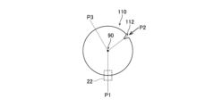
- FIG. 13 is a schematic diagram showing a state before a mounting portion is rotated to detect a mark in an aligner according to an embodiment of the present disclosure.
- FIG. 13 is a schematic diagram showing a state in which a mark overlaps a detection unit in a plan view in an aligner according to an embodiment of the present disclosure.
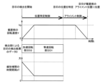
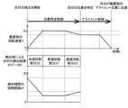
- FIG. 2 is a diagram for explaining position determination control and alignment control of an aligner according to an embodiment of the present disclosure.
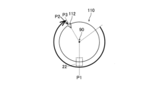
- FIG. 1 is a schematic diagram showing a state in which a mark is positioned at an alignment position in an aligner according to an embodiment of the present disclosure.
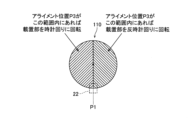
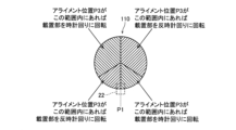
- FIG. 10 is a schematic diagram for explaining a rotation direction of a mounting portion of an aligner according to an embodiment of the present disclosure.
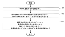
- FIG. 4 is a flow chart showing a process for aligning a semiconductor substrate by an aligner according to an embodiment of the present disclosure.
- FIG. 13 is a schematic diagram showing an aligner according to a first modified example of the present disclosure.
- FIG. 13 is a schematic diagram showing a semiconductor substrate according to a second modified example of the present disclosure.
- FIG. 13 is a schematic diagram for explaining a rotation direction of a mounting portion of an aligner according to a third modified example of the present disclosure.
- 13A and 13B are diagrams for explaining position identification control and alignment control of an aligner according to a fourth modified example of the present disclosure.
- Robot system configuration The configuration of a robot system 100 according to an embodiment of the present disclosure will be described with reference to FIGS. 1 to 6.
- the robot system 100 includes a substrate transport robot 10 that transports a semiconductor substrate 110, and an aligner 20 that aligns the semiconductor substrate 110.
- the semiconductor substrate 110 has a mark 112 formed on a part of an outer periphery 111 for circumferential positioning. Only one mark 112 is provided on the semiconductor substrate 110.
- the mark 112 is a notch.
- the alignment of the semiconductor substrate 110 is performed to correct the substrate transport operation by the robot system 100.
- the substrate transport operation by the robot system 100 includes, for example, an operation of the robot system 10 going to pick up the semiconductor substrate 110, an operation of the robot system 10 placing the semiconductor substrate 110, etc.
- the substrate transport robot 10 includes a hand 11 that holds a semiconductor substrate 110, and a robot arm 12 to the tip of which the hand 11 is attached.
- the substrate transport robot 10 is, for example, a horizontal articulated robot.
- the aligner 20 has a mounting part 21 that rotates around a rotation axis 90 with a semiconductor substrate 110 placed on it.
- the semiconductor substrate 110 is either attached to the mounting part 21 by suction so that the semiconductor substrate 110 can rotate while placed on the mounting part 21, or the mounting surface of the mounting part 21 is processed to generate a frictional force between the semiconductor substrate 110 and the mounting part 21.
- the center of gravity or center of the semiconductor substrate 110 placed on the mounting part 21 may be misaligned with the rotation axis 90 of the mounting part 21.
- the aligner 20 includes a detection unit 22 that detects the mark 112 on the semiconductor substrate 110 placed on the placement unit 21 and rotating around the rotation axis 90.
- the detection unit 22 includes a light-emitting unit that emits light for detection, and a light-receiving unit that receives the light emitted from the light-emitting unit.
- the light-emitting unit and the light-receiving unit are arranged to sandwich the outer periphery 111 of the semiconductor substrate 110.
- the detection unit 22 detects the mark 112 formed on the outer periphery 111 of the semiconductor substrate 110 based on whether or not the light-receiving unit receives the light emitted from the light-emitting unit when the semiconductor substrate 110 is rotating around the rotation axis 90 by rotating the placement unit 21. That is, the detection unit 22 is a transmission type sensor. Only one detection unit 22 is provided on the aligner 20.
- the detection unit 22 may be, for example, a reflective sensor or a camera equipped with an image sensor such as a CCD (Charge Coupled Device) or a CMOS (Complementary Metal Oxide Semiconductor).
- the aligner 20 includes a control unit 23 that controls the rotation of the mounting unit 21.
- the control unit 23 includes, for example, a processor such as a CPU (Central Processing Unit) and a memory that stores information.
- the control unit 23 may be a control unit dedicated to the aligner 20, or may also function as a control unit that controls the robot 10.
- the control unit 23 performs position identification control to identify the position P2 of the mark 112 based on the detection result of the mark 112 by the detection unit 22. Specifically, the control unit 23 rotates the mounting unit 21 in order to detect the mark 112 by the detection unit 22. As shown in FIG. 4, the control unit 23 acquires data D of the detection result of the mark 112 by the detection unit 22 while rotating the mounting unit 21. While rotating the mounting unit 21, the control unit 23 analyzes the acquired data D one by one in the order of acquisition until the position P2 of the mark 112 is identified. In other words, the control unit 23 performs position identification control without stopping the rotation of the mounting unit 21 for detecting the mark 112.
- the control unit 23 performs position identification control using the uniform rotation portion D1 of the data D detected while the placement unit 21 is rotating at a uniform speed, and the accelerated rotation portion D2 detected while the rotation of the placement unit 21 is accelerating. Specifically, after starting the rotation of the placement unit 21, the control unit 23 increases the rotation speed V of the placement unit 21 until it reaches a predetermined rotation speed Vp, and rotates the placement unit 21 at a uniform speed until the position P2 of the mark 112 is identified after the rotation speed V of the placement unit 21 reaches the predetermined rotation speed Vp. The control unit 23 continues to acquire data D from the start of the rotation of the placement unit 21 until the position P2 of the mark 112 is identified. The data D includes only the uniform rotation portion D1 and the accelerated rotation portion D2.
- the data D for detecting the mark 112 is sufficient for the placement unit 21 to rotate 360 degrees, so the rotation angle of the placement unit 21 corresponding to the uniform rotation portion D1 is less than 360 degrees. That is, the control unit 23 performs position identification control using the accelerated rotation portion D2 in addition to the uniform rotation portion D1 of the data D that is detected while the placement unit 21 is rotating at a uniform speed of less than 360 degrees.
- the control unit 23 performs position identification control using the uniform rotation portion D1 of the data D and the accelerated rotation portion D2 in which the time interval dT of the linear interpolation for analyzing the data D is adjusted according to the magnitude of the rotation speed of the mounting unit 21. Specifically, the control unit 23 performs position identification control using the uniform rotation portion D1 of the data D and the accelerated rotation portion D2 in which the time interval dT of the linear interpolation is adjusted to gradually decrease as the rotation speed of the mounting unit 21 increases. That is, the uniform rotation portion D1 of the data D used for position identification control is linearly interpolated at a constant time interval dT.
- the time interval dT of the linear interpolation in the accelerated rotation portion D2 of the data D used for position identification control is adjusted so that the rotation angle of the mounting unit 21 per unit time corresponding to the uniform rotation portion D1 and the rotation angle of the mounting unit 21 per unit time corresponding to the accelerated rotation portion D2 are approximately equal.
- the control unit 23 performs alignment control to rotate the mounting unit 21 so as to align the semiconductor substrate 110 based on the identified position P2 of the mark 112. Specifically, as shown in Fig. 3 and Fig. 5, after the position P2 of the mark 112 is identified, the control unit 23 rotates the mounting unit 21 until the mark 112 is located at the alignment position P3. Note that the alignment position P3 is the target position of the mark 112 in the alignment control.
- the control unit 23 After the position P2 of the mark 112 is identified, the control unit 23 performs alignment control without stopping the rotation of the mounting unit 21 and while maintaining the rotational direction of the mounting unit 21. That is, as shown in Figures 2, 3 and 5, the control unit 23 continues to rotate the mounting unit 21 in the same direction from when it starts rotating the mounting unit 21 to detect the mark 112 with the detection unit 22 until the mark 112 is located at the alignment position P3. Note that Figures 2, 3 and 5 show an example in which the mounting unit 21 is rotated clockwise.
- the control unit 23 When performing eccentricity analysis control to analyze eccentricity, which is the deviation of the center of gravity or center of the semiconductor substrate 110 relative to the rotation axis 90 of the placement unit 21, the control unit 23 performs alignment control after the position P2 of the mark 112 is identified and after the placement unit 21 has rotated at least approximately 180 degrees after starting rotation for identifying the position P2 of the mark 112. Specifically, when it is necessary to perform eccentricity analysis control, even after the position P2 of the mark 112 is identified, alignment control is not performed until the placement unit 21 has rotated at least approximately 180 degrees required for eccentricity analysis control after starting rotation for identifying the position P2 of the mark 112.
- eccentricity analysis control is performed based on detection data for approximately 180 degrees of the outer periphery 111 of the semiconductor substrate 110 in order to detect the center of gravity or center of the semiconductor substrate 110.
- Information on the center of gravity or center of the semiconductor substrate 110 acquired by eccentricity analysis control is used to correct the substrate transport operation by the robot system 100.
- the control unit 23 determines the rotation direction of the mounting unit 21 for detecting the mark 112 by the detection unit 22 based on the relationship between the position P1 of the detection unit 22 relative to the mounting unit 21 before the rotation of the mounting unit 21 and the alignment position P3. Specifically, as shown in FIG. 6, the control unit 23 determines the rotation of the mounting unit 21 for detecting the mark 112 by the detection unit 22 in a direction closer to the alignment position P3 as viewed from the position P1 of the detection unit 22 relative to the mounting unit 21 before the rotation of the mounting unit 21.
- the control unit 23 continues to rotate the mounting unit 21 clockwise after starting the rotation of the mounting unit 21 for detecting the mark 112 by the detection unit 22 until the mark 112 is located at the alignment position P3.
- the position P1 of the detection unit 22 is in the 6 o'clock direction and the alignment position P3 is within the range between the 0 o'clock direction and the 6 o'clock direction, the placement unit 21 continues to rotate counterclockwise.
- the placement unit 21 continues to rotate counterclockwise after the rotation of the placement unit 21 for detecting the mark 112 by the detection unit 22 is started until the mark 112 is located at the alignment position P3.
- the semiconductor substrate 110 is likened to a clock
- the position P1 of the detection unit 22 is in the 6 o'clock direction and the alignment position P3 is within the range between the 6 o'clock direction and the 12 o'clock direction, the placement unit 21 continues to rotate clockwise.
- Method for aligning a semiconductor substrate A method for aligning the semiconductor substrate 110 will be described with reference to FIG.
- step S1 the mark 112 on the semiconductor substrate 110 placed on the placement unit 21 and rotating around the rotation axis 90 is detected.
- step S2 the position P2 of the mark 112 is identified based on the detection result of the mark 112 without stopping the rotation of the mounting unit 21 for detecting the mark 112. Note that step S2 is not started after step S1 is completed, but is carried out substantially in parallel with step S1.
- step S3 after the position P2 of the mark 112 is identified, the mounting part 21 is rotated so as to align the semiconductor substrate 110 based on the identified position P2 of the mark 112, without stopping the rotation of the mounting part 21 and while maintaining the rotational direction of the mounting part 21.
- the control unit 23 performs position identification control without stopping the rotation of the mounting unit 21 to detect the mark 112, and performs alignment control without stopping the rotation of the mounting unit 21 and maintaining the rotation direction of the mounting unit 21 after the position P2 of the mark 112 is identified.
- the mounting unit 21 continues to rotate in the same direction without stopping it from when the mounting unit 21 is rotated to detect the mark 112 until the mark 112 is located at the alignment position P3. Therefore, the time required to decelerate and accelerate the rotation of the mounting unit 21 can be shortened compared to when the rotation of the mounting unit 21 is temporarily stopped or when the rotation direction of the mounting unit 21 is changed midway. As a result, the overall time required to align the semiconductor substrate 110 can be shortened.
- control unit 23 performs position identification control using the accelerated rotation portion D2 detected while accelerating the rotation of the mounting unit 21 in addition to the uniform rotation portion D1 detected while rotating the mounting unit 21 at a uniform speed, out of the data D of the detection result of the mark 112 by the detection unit 22.
- This makes it possible to reduce the rotation angle range of the mounting unit 21 for acquiring the uniform rotation portion D1 required for position identification control by the amount of the accelerated rotation portion D2 used for position identification control.
- the time required for position identification control can be shortened compared to when the accelerated rotation portion D2 is not used for position identification control, and therefore the overall time required for aligning the semiconductor substrate 110 can be shortened.
- control unit 23 performs position identification control using the accelerated rotation portion D2 of the data D in addition to the uniform rotation portion D1 detected while the mounting unit 21 is rotating at a uniform speed of less than 360 degrees. This makes it possible to reduce the rotation angle range of the mounting unit 21 for acquiring the uniform rotation portion D1 compared to when the uniform rotation portion D1 is 360 degrees or more. As a result, the time required for position identification control can be shortened compared to when the uniform rotation portion D1 is 360 degrees or more, and therefore the overall time required for aligning the semiconductor substrate 110 can be shortened.
- the control unit 23 performs position identification control using, in addition to the constant speed rotation portion D1 of the data D, the accelerated rotation portion D2 in which the time interval of linear interpolation for analyzing the data D is adjusted according to the magnitude of the rotation speed of the mounting unit 21.
- the control unit 23 performs position identification control using, in addition to the constant speed rotation portion D1 of the data D, the accelerated rotation portion D2 in which the time interval of linear interpolation for analyzing the data D is adjusted according to the magnitude of the rotation speed of the mounting unit 21.
- the control unit 23 performs position identification control using, in addition to the uniform rotation portion D1 of the data D, an accelerated rotation portion D2 in which the time interval dT of linear interpolation is adjusted to gradually decrease as the rotation speed of the mounting unit 21 increases.
- This makes it possible to adjust the time interval dT of linear interpolation for the accelerated rotation portion D2 so that the rotation angle of the mounting unit 21 per unit time corresponding to the uniform rotation portion D1 and the rotation angle of the mounting unit 21 per unit time corresponding to the accelerated rotation portion D2 are approximately equal, thereby ensuring that the accuracy of linear interpolation is equal between the uniform rotation portion D1 and the accelerated rotation portion D2.
- the accelerated rotation portion D2 is used for position identification control in addition to the uniform rotation portion D1, it is possible to reliably prevent the accuracy of the position identification control from decreasing.
- control unit 23 determines the rotation direction of the placement unit 21 for detecting the mark 112 by the detection unit 22 based on the relationship between the position P1 of the detection unit 22 relative to the placement unit 21 before the rotation of the placement unit 21 and the alignment position P3, which is the target position of the mark 112 in the alignment control.
- the rotation direction of the placement unit 21 can be determined so that the rotation angle range of the placement unit 21 until the mark 112 is positioned at the alignment position P3 is small in the alignment control performed after the position identification control.
- the time required for alignment control can be shortened compared to when the rotation direction of the placement unit 21 is determined without considering the relationship between the position P1 of the detection unit 22 relative to the placement unit 21 before the rotation of the placement unit 21 and the alignment position P3, and therefore the overall time required for aligning the semiconductor substrate 110 can be shortened.
- control unit 23 rotates the placement unit 21 to detect the mark 112 by the detection unit 22 in a direction closer to the alignment position P3 as viewed from the position P1 of the detection unit 22 relative to the placement unit 21 before the rotation of the placement unit 21.
- This makes it possible to reduce the rotation angle range of the placement unit 21 until the mark 112 is positioned at the alignment position P3 in the alignment control performed after the position identification control, compared to when the placement unit 21 is rotated in a direction farther from the alignment position P3 as viewed from the position P1 of the detection unit 22 relative to the placement unit 21 before the rotation of the placement unit 21.
- the time required for the alignment control can be shortened, compared to when the placement unit 21 is rotated in a direction farther from the alignment position P3 as viewed from the position P1 of the detection unit 22 relative to the placement unit 21 before the rotation of the placement unit 21, and therefore the overall time required for aligning the semiconductor substrate 110 can be shortened.
- the control unit 23 when performing eccentricity analysis control to analyze eccentricity, which is the deviation of the center of gravity or center of the semiconductor substrate 110 relative to the rotation axis 90 of the mounting unit 21, the control unit 23 performs alignment control after the position P2 of the mark 112 is identified and after the mounting unit 21 has rotated at least approximately 180 degrees after starting rotation for identifying the position P2 of the mark 112.
- alignment control is not performed until the mounting unit 21 has rotated at least approximately 180 degrees required for eccentricity analysis control after starting rotation for identifying the position P2 of the mark 112, thereby making it possible to reliably perform eccentricity analysis control.
- the rotation of the mounting unit 21 for position identification control and the rotation of the mounting unit 21 for eccentricity analysis control can be made common, the overall time required for aligning the semiconductor substrate 110 can be shortened.
- the mark 112 is a notch. This can reduce the overall time required to align the semiconductor substrate 110 whose mark 112 is a notch.
- the position P2 of the mark 112 is specified based on the detection result of the mark 112 without stopping the rotation of the placement part 21 for detecting the mark 112, and after the position P2 of the mark 112 is specified, the placement part 21 is rotated so as to align the semiconductor substrate 110 based on the specified position P2 of the mark 112 without stopping the rotation of the placement part 21 and while maintaining the rotation direction of the placement part 21.
- the placement part 21 is rotated to detect the mark 112 and continues to rotate in the same direction without stopping until the mark 112 is positioned at the alignment position P3, the time for decelerating and accelerating the rotation of the placement part 21 can be shortened compared to the case where the rotation of the placement part 21 is temporarily stopped or the rotation direction of the placement part 21 is changed midway. As a result, similar to the effects of the robot system 100 and the aligner 20, the overall time required for aligning the semiconductor substrate 110 can be shortened.
- FIG. 8 shows an example in which two detection units 22 are provided at intervals of approximately 180 degrees around the rotation axis 90.
- the mark 112 was a notch
- the present disclosure is not limited to this.
- the mark 212 may be an orientation flat, as in the semiconductor substrate 210 of the second modified example shown in FIG. 9. This can reliably shorten the overall time required to align the semiconductor substrate 210 whose mark 212 is an orientation flat.
- control unit 23 when the control unit 23 performs eccentricity analysis control to analyze eccentricity, which is the deviation of the center of gravity or center of the semiconductor substrate 110 relative to the rotation axis 90 of the mounting unit 21, an example has been shown in which the control unit performs alignment control after the position P2 of the mark 112 has been identified and after the mounting unit 21 has rotated at least approximately 180 degrees or more since starting rotation to identify the position P2 of the mark 112, but the present disclosure is not limited to this.
- control unit when the control unit does not perform eccentricity analysis control to analyze eccentricity, which is the deviation of the center of gravity or center of the semiconductor substrate relative to the rotation axis of the mounting unit, the control unit may perform alignment control after the position of the mark has been identified, regardless of whether the mounting unit has rotated at least approximately 180 degrees or more since starting rotation to identify the position of the mark.
- control unit 23 determines the rotation direction of the mounting unit 21 for detecting the mark 112 by the detection unit 22 in a direction closer to the alignment position P3 as viewed from the position P1 of the detection unit 22 relative to the mounting unit 21 before the rotation of the mounting unit 21, but the present disclosure is not limited to this.
- the present disclosure as in the third modified example shown in FIG.
- the rotation direction of the mounting unit 21 may be determined based on which of three or more regions the alignment position P3 is in, rather than on which of two regions the alignment position P3 is in, as in the case where the rotation direction of the mounting unit 21 is determined in a direction closer to the alignment position P3 as viewed from the position P1 of the detection unit 22 relative to the mounting unit 21 before the rotation of the mounting unit 21.
- the rotation direction of the placement part 21 is determined depending on which of the four regions the alignment position P3 of the placement part 21 is in. Specifically, in Fig. 10, when the semiconductor substrate 110 is likened to a clock, if the position P1 of the detection part 22 is in the 6 o'clock direction and the alignment position P3 is within the range between the 0 o'clock direction and the 4 o'clock direction, or within the range between the 6 o'clock direction and the 8 o'clock direction, the placement part 21 continues to rotate counterclockwise, and if the alignment position P3 of the semiconductor substrate 110 is within the range between the 4 o'clock direction and the 6 o'clock direction, or within the range between the 8 o'clock direction and the 12 o'clock direction, or within the range between the 4 o'clock direction and the 6 o'clock direction, the placement part 21 continues to rotate clockwise.
- control unit 23 determines the rotation direction of the mounting unit 21 for detecting the mark 112 by the detection unit 22 based on the relationship between the position P1 of the detection unit 22 relative to the mounting unit 21 before the rotation of the mounting unit 21 and the alignment position P3, but the present disclosure is not limited to this.
- the control unit may determine the rotation direction of the mounting unit for detecting the mark by the detection unit without being based on the relationship between the position of the detection unit relative to the mounting unit before the rotation of the mounting unit and the alignment position.
- control unit 23 performs position identification control by using the accelerated rotation portion D2 in which the time interval dT of the linear interpolation is adjusted to gradually decrease as the rotation speed of the mounting unit 21 increases, in addition to the uniform rotation portion D1 of the data D. That is, the control unit 23 performs position identification control by using the accelerated rotation portion D2 in which the time interval dT of the linear interpolation for analyzing the data D is adjusted according to the magnitude of the rotation speed of the mounting unit 21, in addition to the uniform rotation portion D1 of the data D, but the present disclosure is not limited to this.
- control unit may perform position identification control by using the accelerated rotation portion in which the time interval of the linear interpolation is not adjusted to gradually decrease as the rotation speed of the mounting unit increases, in addition to the uniform rotation portion of the data. That is, the control unit may perform position identification control by using the accelerated rotation portion in which the time interval of the linear interpolation for analyzing the data is not adjusted according to the magnitude of the rotation speed of the mounting unit, in addition to the uniform rotation portion of the data.
- the data D includes only the uniform rotation portion D1 and the accelerated rotation portion D2, and the control unit 23 performs position identification control using the uniform rotation portion D1 and the accelerated rotation portion D2 of the data D, but the present disclosure is not limited to this.
- the control unit 23 may perform position identification control using the decelerated rotation portion D3 detected while the rotation of the mounting unit 21 is being decelerated in addition to the uniform rotation portion D1 and the accelerated rotation portion D2 of the data D.
- the rotation angle range of the mounting unit 21 for acquiring the uniform rotation portion D1 required for position identification control can be reduced by the amount of the decelerated rotation portion D3 used for position identification control.
- the time required for position determination control can be shortened compared to when the decelerated rotation portion D3 is not used for position determination control, and therefore the overall time required for aligning the semiconductor substrate 110 can be shortened.
- control unit 23 performs position identification control using the accelerated rotation portion D2 of the data D in addition to the uniform rotation portion D1 detected while the placement unit 21 is rotating at a uniform speed less than 360 degrees, but the present disclosure is not limited to this.
- control unit may perform position identification control using the accelerated rotation portion of the data in addition to the uniform rotation portion detected while the placement unit is rotating at a uniform speed of 360 degrees or more.
- control unit 23 performs position identification control using the accelerated rotation portion D2 detected while the rotation of the mounting unit 21 is accelerating in addition to the uniform rotation portion D1 detected while the rotation of the mounting unit 21 is being accelerated, out of the data D of the detection result of the mark 112 by the detection unit 22, but the present disclosure is not limited to this.
- the control unit may perform position identification control using only the uniform rotation portion detected while the mounting unit is rotating at a uniform speed, without using the accelerated rotation portion detected while the rotation of the mounting unit is accelerating, out of the data of the detection result of the mark 112 by the detection unit.
- the detection unit 22 detects the mark 112 on the semiconductor substrate 110, and the control unit 23 identifies the position P2 of the mark 112 based on the detection result of the mark 112 by the detection unit 22, but the present disclosure is not limited to this.
- the detection unit may detect defects in the semiconductor substrate in addition to the marks on the semiconductor substrate, and the control unit may identify the position of the defect based on the detection result of the defect by the detection unit in addition to identifying the position of the mark based on the mark detection result by the detection unit.
- circuits or processing circuits including general purpose processors, special purpose processors, integrated circuits, ASICs (Application Specific Integrated Circuits), conventional circuits, and/or combinations thereof, configured or programmed to perform the disclosed functions.
- Processors are considered processing circuits or circuits because they include transistors and other circuits.
- a circuit, unit, or means is hardware that performs the recited functions or hardware that is programmed to perform the recited functions.
- the hardware may be hardware disclosed herein or other known hardware that is programmed or configured to perform the recited functions. Where the hardware is a processor, which is considered a type of circuit, the circuit, means, or unit is a combination of hardware and software, and the software is used to configure the hardware and/or the processor.
- a substrate transport robot that transports a semiconductor substrate having a mark formed on an outer periphery thereof for circumferential positioning; an aligner for aligning the semiconductor substrate;
- the aligner comprises: a mounting part that rotates around a rotation axis with the semiconductor substrate mounted thereon; a detection unit that detects the mark of the semiconductor substrate that is placed on the placement unit and rotates around the rotation axis; a control unit that performs position identification control to identify a position of the mark based on a detection result of the mark by the detection unit, and performs alignment control to rotate the placement unit so as to align the semiconductor substrate based on the identified position of the mark,
- the control unit performs the position identification control without stopping the rotation of the placement unit to detect the mark, and after the position of the mark is identified, performs the alignment control without stopping the rotation of the placement unit and while maintaining the rotational direction of the placement unit.
- (Item 2) 2. The robot system according to claim 1, wherein the control unit performs the position identification control using an accelerated rotation portion detected while accelerating the rotation of the placement unit in addition to a constant speed rotation portion detected while the placement unit is rotating at a constant speed, out of the data of the detection result of the mark by the detection unit.
- (Item 4) 4. The robot system according to claim 2, wherein the control unit performs the position identification control by using a decelerating rotation portion detected while decelerating the rotation of the placement unit in addition to the constant rotation portion and the accelerating rotation portion of the data.
- control unit performs the position identification control by using, in addition to the constant speed rotation portion of the data, the accelerated rotation portion in which a time interval of the linear interpolation for analyzing the data is adjusted depending on a magnitude of the rotation speed of the placement unit.
- (Item 7) The robot system according to any one of items 1 to 6, wherein the control unit determines a rotation direction of the placement unit for detecting the mark by the detection unit based on a relationship between a position of the detection unit relative to the placement unit before rotation of the placement unit and an alignment position, which is a target position of the mark in the alignment control.
- An aligner for aligning a semiconductor substrate having a mark formed on an outer periphery thereof for performing circumferential positioning, a mounting part that rotates around a rotation axis with the semiconductor substrate mounted thereon; a detection unit that detects the mark of the semiconductor substrate that is placed on the placement unit and rotates around the rotation axis; a control unit that performs position identification control to identify a position of the mark based on a detection result of the mark by the detection unit, and performs alignment control to rotate the placement unit so as to align the semiconductor substrate based on the identified position of the mark, The control unit performs the position identification control without stopping the rotation of the placement unit for detecting the mark, and after the position of the mark is identified, performs the alignment control without stopping the rotation of the placement unit and while maintaining the rotational direction of the placement unit.
- a method for aligning a semiconductor substrate having a mark formed on an outer periphery thereof for performing circumferential positioning comprising the steps of: detecting the mark on the semiconductor substrate placed on a placement part and rotating about a rotation axis; identifying a position of the mark based on a result of the detection of the mark without stopping the rotation of the placement unit for detecting the mark;
- a method for aligning a semiconductor substrate comprising: after the position of the mark is identified, rotating the placement portion so as to align the semiconductor substrate based on the identified position of the mark, without stopping the rotation of the placement portion and while maintaining the rotational direction of the placement portion.
Landscapes
- Container, Conveyance, Adherence, Positioning, Of Wafer (AREA)
- Engineering & Computer Science (AREA)
- Robotics (AREA)
Abstract
Description
図1から図6までを参照して、本開示の一実施形態によるロボットシステム100の構成について説明する。
図1に示すように、ロボットシステム100は、半導体基板110を搬送する基板搬送ロボット10と、半導体基板110をアライメントするためのアライナ20と、を備える。半導体基板110は、外周部111の一部に周方向の位置決めを行うための目印112が形成されている。目印112は、半導体基板110に1つだけ設けられている。目印112は、ノッチである。なお、半導体基板110のアライメントは、ロボットシステム100による基板搬送の動作を補正するために行われる。ロボットシステム100による基板搬送の動作は、たとえば、ロボットシステム10による半導体基板110を取りに行く動作、ロボットシステム10による半導体基板110を置く動作、等である。
図2および図3に示すように、制御部23は、検出部22による目印112の検出結果に基づいて目印112の位置P2を特定する位置特定制御を行う。具体的には、制御部23は、検出部22により目印112を検出するために、載置部21を回転させる。図4に示すように、制御部23は、載置部21を回転させながら、検出部22による目印112の検出結果のデータDを取得する。制御部23は、載置部21を回転させながら、取得したデータDを、目印112の位置P2が特定されるまで、取得した順に逐一解析する。すなわち、制御部23は、目印112を検出するための載置部21の回転を停止させずに、位置特定制御を行う。
制御部23は、特定した目印112の位置P2に基づいて半導体基板110をアライメントするように載置部21を回転させるアライメント制御を行う。具体的には、図3および図5に示すように、制御部23は、目印112の位置P2が特定された後、目印112がアライメント位置P3に位置するまで、載置部21を回転させる。なお、アライメント位置P3は、アライメント制御における目印112の目標位置である。
図7を参照して、半導体基板110のアライメント方法について説明する。
本実施形態では、以下のような効果を得ることができる。
本実施形態では、制御部23は、目印112を検出するための載置部21の回転を停止させずに、位置特定制御を行うとともに、目印112の位置P2が特定された後、載置部21の回転を停止させずに、かつ、載置部21の回転方向を維持したまま、アライメント制御を行う。これにより、目印112を検出するために載置部21を回転させてから、目印112がアライメント位置P3に位置するまで、載置部21を停止させることなく同じ方向に回転させ続けるので、載置部21の回転を一旦停止させる場合、載置部21の回転方向を途中で変える場合等と比較して、載置部21の回転を減速および加速させる時間を短くすることができる。その結果、半導体基板110をアライメントするための全体的な所要時間を短くすることができる。
本実施形態では、目印112を検出するための載置部21の回転を停止させずに、目印112の検出結果に基づいて目印112の位置P2を特定することが行われるとともに、目印112の位置P2が特定された後、載置部21の回転を停止させずに、かつ、載置部21の回転方向を維持したまま、特定した目印112の位置P2に基づいて半導体基板110をアライメントするように載置部21を回転させることが行われる。これにより、目印112を検出するために載置部21を回転させてから、目印112がアライメント位置P3に位置するまで、載置部21を停止させることなく同じ方向に回転させ続けるので、載置部21の回転を一旦停止させる場合、載置部21の回転方向を途中で変える場合等と比較して、載置部21の回転を減速および加速させる時間を短くすることができる。その結果、ロボットシステム100およびアライナ20の効果と同様に、半導体基板110をアライメントするための全体的な所要時間を短くすることができる。
今回開示された実施形態は、全ての点で例示であり制限的なものではないと考えられるべきである。本開示の範囲は、上記した実施形態の説明ではなく請求の範囲によって示され、さらに請求の範囲と均等の意味および範囲内での全ての変更(変形例)が含まれる。
上記した例示的な実施形態は、以下の態様の具体例であることが当業者により理解される。
外周部に周方向の位置決めを行うための目印が形成された半導体基板を搬送する基板搬送ロボットと、
前記半導体基板をアライメントするためのアライナと、を備え、
前記アライナは、
前記半導体基板を載置した状態で回転軸線周りに回転する載置部と、
前記載置部に載置され前記回転軸線回りに回転する前記半導体基板の前記目印を検出する検出部と、
前記検出部による前記目印の検出結果に基づいて前記目印の位置を特定する位置特定制御を行うとともに、前記特定した前記目印の位置に基づいて前記半導体基板をアライメントするように前記載置部を回転させるアライメント制御を行う制御部と、を備え、
前記制御部は、前記目印を検出するための前記載置部の回転を停止させずに、前記位置特定制御を行うとともに、前記目印の位置が特定された後、前記載置部の回転を停止させずに、かつ、前記載置部の回転方向を維持したまま、前記アライメント制御を行う、ロボットシステム。
前記制御部は、前記検出部による前記目印の前記検出結果のデータのうちの、前記載置部を等速で回転させている間に検出された等速回転部分に加えて、前記載置部の回転を加速させている間に検出された加速回転部分を用いて、前記位置特定制御を行う、項目1に記載のロボットシステム。
前記制御部は、前記データのうちの、前記載置部を等速で360度未満回転させている間に検出された前記等速回転部分に加えて、前記加速回転部分を用いて、前記位置特定制御を行う、項目2に記載のロボットシステム。
前記制御部は、前記データのうちの、前記等速回転部分および前記加速回転部分に加えて、前記載置部の回転を減速させている間に検出された減速回転部分を用いて、前記位置特定制御を行う、項目2または項目3に記載のロボットシステム。
前記制御部は、前記データのうちの、前記等速回転部分に加えて、前記載置部の回転速度の大きさに応じて前記データを解析するための前記線形補間の時間間隔が調整された前記加速回転部分を用いて、前記位置特定制御を行う、項目2から項目4までのいずれか1項に記載のロボットシステム。
前記制御部は、前記データのうちの、前記等速回転部分に加えて、前記載置部の回転速度が大きくなるにしたがって前記線形補間の時間間隔が徐々に小さくなるように調整された前記加速回転部分を用いて、前記位置特定制御を行う、項目5に記載のロボットシステム。
前記制御部は、前記検出部により前記目印を検出するための前記載置部の回転方向を、前記載置部の回転前の前記載置部に対する前記検出部の位置と、前記アライメント制御における前記目印の目標位置であるアライメント位置との関係に基づいて決定する、項目1から項目6までのいずれか1項に記載のロボットシステム。
前記制御部は、前記検出部により前記目印を検出するための前記載置部の回転方向を、前記載置部の回転前の前記載置部に対する前記検出部の位置から見て前記アライメント位置に対して近い方向に決定する、項目7に記載のロボットシステム。
前記制御部は、前記載置部の前記回転軸線に対する前記半導体基板の重心または中心のずれである偏心を解析する偏心解析制御を行う場合、前記目印の位置が特定された後、かつ、前記載置部が前記目印の位置の特定のための回転を開始してから少なくとも略180度以上回転した後に、前記アライメント制御を行う、項目1から項目8までのいずれか1項に記載のロボットシステム。
前記目印は、ノッチである、項目1から項目9までのいずれか1項に記載のロボットシステム。
前記目印は、オリエンテーションフラットである、項目1から項目9までのいずれか1項に記載のロボットシステム。
外周部に周方向の位置決めを行うための目印が形成された半導体基板をアライメントするためのアライナであって、
前記半導体基板を載置した状態で回転軸線周りに回転する載置部と、
前記載置部に載置され前記回転軸線回りに回転する前記半導体基板の前記目印を検出する検出部と、
前記検出部による前記目印の検出結果に基づいて前記目印の位置を特定する位置特定制御を行うとともに、前記特定した前記目印の位置に基づいて前記半導体基板をアライメントするように前記載置部を回転させるアライメント制御を行う制御部と、を備え、
前記制御部は、前記目印を検出するための前記載置部の回転を停止させずに、前記位置特定制御を行うとともに、前記目印の位置が特定された後、前記載置部の回転を停止させずに、かつ、前記載置部の回転方向を維持したまま、前記アライメント制御を行う、アライナ。
外周部に周方向の位置決めを行うための目印が形成された半導体基板のアライメント方法であって、
載置部に載置され回転軸線回りに回転する前記半導体基板の前記目印を検出することと、
前記目印を検出するための前記載置部の回転を停止させずに、前記目印の検出結果に基づいて前記目印の位置を特定することと、
前記目印の位置が特定された後、前記載置部の回転を停止させずに、かつ、前記載置部の回転方向を維持したまま、特定した前記目印の位置に基づいて前記半導体基板をアライメントするように前記載置部を回転させることと、を備える、半導体基板のアライメント方法。
Claims (13)
- 外周部に周方向の位置決めを行うための目印が形成された半導体基板を搬送する基板搬送ロボットと、
前記半導体基板をアライメントするためのアライナと、を備え、
前記アライナは、
前記半導体基板を載置した状態で回転軸線周りに回転する載置部と、
前記載置部に載置され前記回転軸線回りに回転する前記半導体基板の前記目印を検出する検出部と、
前記検出部による前記目印の検出結果に基づいて前記目印の位置を特定する位置特定制御を行うとともに、前記特定した前記目印の位置に基づいて前記半導体基板をアライメントするように前記載置部を回転させるアライメント制御を行う制御部と、を備え、
前記制御部は、前記目印を検出するための前記載置部の回転を停止させずに、前記位置特定制御を行うとともに、前記目印の位置が特定された後、前記載置部の回転を停止させずに、かつ、前記載置部の回転方向を維持したまま、前記アライメント制御を行う、ロボットシステム。 - 前記制御部は、前記検出部による前記目印の前記検出結果のデータのうちの、前記載置部を等速で回転させている間に検出された等速回転部分に加えて、前記載置部の回転を加速させている間に検出された加速回転部分を用いて、前記位置特定制御を行う、請求項1に記載のロボットシステム。
- 前記制御部は、前記データのうちの、前記載置部を等速で360度未満回転させている間に検出された前記等速回転部分に加えて、前記加速回転部分を用いて、前記位置特定制御を行う、請求項2に記載のロボットシステム。
- 前記制御部は、前記データのうちの、前記等速回転部分および前記加速回転部分に加えて、前記載置部の回転を減速させている間に検出された減速回転部分を用いて、前記位置特定制御を行う、請求項2に記載のロボットシステム。
- 前記制御部は、前記データのうちの、前記等速回転部分に加えて、前記載置部の回転速度の大きさに応じて前記データを解析するための前記線形補間の時間間隔が調整された前記加速回転部分を用いて、前記位置特定制御を行う、請求項2に記載のロボットシステム。
- 前記制御部は、前記データのうちの、前記等速回転部分に加えて、前記載置部の回転速度が大きくなるにしたがって前記線形補間の時間間隔が徐々に小さくなるように調整された前記加速回転部分を用いて、前記位置特定制御を行う、請求項5に記載のロボットシステム。
- 前記制御部は、前記検出部により前記目印を検出するための前記載置部の回転方向を、前記載置部の回転前の前記載置部に対する前記検出部の位置と、前記アライメント制御における前記目印の目標位置であるアライメント位置との関係に基づいて決定する、請求項1に記載のロボットシステム。
- 前記制御部は、前記検出部により前記目印を検出するための前記載置部の回転方向を、前記載置部の回転前の前記載置部に対する前記検出部の位置から見て前記アライメント位置に対して近い方向に決定する、請求項7に記載のロボットシステム。
- 前記制御部は、前記載置部の前記回転軸線に対する前記半導体基板の重心または中心のずれである偏心を解析する偏心解析制御を行う場合、前記目印の位置が特定された後、かつ、前記載置部が前記目印の位置の特定のための回転を開始してから少なくとも略180度以上回転した後に、前記アライメント制御を行う、請求項1に記載のロボットシステム。
- 前記目印は、ノッチである、請求項1に記載のロボットシステム。
- 前記目印は、オリエンテーションフラットである、請求項1に記載のロボットシステム。
- 外周部に周方向の位置決めを行うための目印が形成された半導体基板をアライメントするためのアライナであって、
前記半導体基板を載置した状態で回転軸線周りに回転する載置部と、
前記載置部に載置され前記回転軸線回りに回転する前記半導体基板の前記目印を検出する検出部と、
前記検出部による前記目印の検出結果に基づいて前記目印の位置を特定する位置特定制御を行うとともに、前記特定した前記目印の位置に基づいて前記半導体基板をアライメントするように前記載置部を回転させるアライメント制御を行う制御部と、を備え、
前記制御部は、前記目印を検出するための前記載置部の回転を停止させずに、前記位置特定制御を行うとともに、前記目印の位置が特定された後、前記載置部の回転を停止させずに、かつ、前記載置部の回転方向を維持したまま、前記アライメント制御を行う、アライナ。 - 外周部に周方向の位置決めを行うための目印が形成された半導体基板のアライメント方法であって、
載置部に載置され回転軸線回りに回転する前記半導体基板の前記目印を検出することと、
前記目印を検出するための前記載置部の回転を停止させずに、前記目印の検出結果に基づいて前記目印の位置を特定することと、
前記目印の位置が特定された後、前記載置部の回転を停止させずに、かつ、前記載置部の回転方向を維持したまま、特定した前記目印の位置に基づいて前記半導体基板をアライメントするように前記載置部を回転させることと、を備える、半導体基板のアライメント方法。
Priority Applications (3)
| Application Number | Priority Date | Filing Date | Title |
|---|---|---|---|
| KR1020257012178A KR20250069630A (ko) | 2022-10-05 | 2023-10-05 | 로봇 시스템, 얼라이너 및 반도체 기판의 얼라인먼트 방법 |
| US19/113,631 US20260101711A1 (en) | 2022-10-05 | 2023-10-05 | Robot system, aligner, and aligning semiconductor substrate |
| CN202380070809.9A CN119998941A (zh) | 2022-10-05 | 2023-10-05 | 机器人系统、对准器以及半导体基板的对准方法 |
Applications Claiming Priority (2)
| Application Number | Priority Date | Filing Date | Title |
|---|---|---|---|
| JP2022-160989 | 2022-10-05 | ||
| JP2022160989A JP2024054636A (ja) | 2022-10-05 | 2022-10-05 | ロボットシステム、アライナおよび半導体基板のアライメント方法 |
Publications (1)
| Publication Number | Publication Date |
|---|---|
| WO2024075818A1 true WO2024075818A1 (ja) | 2024-04-11 |
Family
ID=90608501
Family Applications (1)
| Application Number | Title | Priority Date | Filing Date |
|---|---|---|---|
| PCT/JP2023/036406 Ceased WO2024075818A1 (ja) | 2022-10-05 | 2023-10-05 | ロボットシステム、アライナおよび半導体基板のアライメント方法 |
Country Status (6)
| Country | Link |
|---|---|
| US (1) | US20260101711A1 (ja) |
| JP (1) | JP2024054636A (ja) |
| KR (1) | KR20250069630A (ja) |
| CN (1) | CN119998941A (ja) |
| TW (1) | TWI875229B (ja) |
| WO (1) | WO2024075818A1 (ja) |
Families Citing this family (2)
| Publication number | Priority date | Publication date | Assignee | Title |
|---|---|---|---|---|
| JP2021023320A (ja) * | 2019-07-31 | 2021-02-22 | 株式会社三洋物産 | 遊技機 |
| JP2021023319A (ja) * | 2019-07-31 | 2021-02-22 | 株式会社三洋物産 | 遊技機 |
Citations (5)
| Publication number | Priority date | Publication date | Assignee | Title |
|---|---|---|---|---|
| JP2001093828A (ja) * | 2000-07-14 | 2001-04-06 | Tokyo Electron Ltd | 処理システム |
| JP2003188235A (ja) * | 2001-10-12 | 2003-07-04 | Ckd Corp | アライナ装置 |
| JP2014060373A (ja) * | 2012-09-19 | 2014-04-03 | Sumitomo Precision Prod Co Ltd | アライメント装置およびそのための回転条件調整方法および装置、並びに基板処理装置 |
| JP2018056339A (ja) * | 2016-09-29 | 2018-04-05 | 株式会社Screenホールディングス | 基板搬送装置および基板搬送方法 |
| JP2021044548A (ja) * | 2019-09-06 | 2021-03-18 | 株式会社安川電機 | ウェハプリアライナおよびウェハのプリアライメント方法 |
Family Cites Families (3)
| Publication number | Priority date | Publication date | Assignee | Title |
|---|---|---|---|---|
| KR100271361B1 (ko) * | 1997-08-30 | 2001-01-15 | 윤종용 | 웨이퍼얼라인장치및그방법 |
| JP6285275B2 (ja) * | 2014-04-30 | 2018-02-28 | 株式会社Screenホールディングス | 基板処理装置および基板処理方法 |
| JP2022048506A (ja) * | 2020-09-15 | 2022-03-28 | 株式会社ダイヘン | アライナ装置 |
-
2022
- 2022-10-05 JP JP2022160989A patent/JP2024054636A/ja active Pending
-
2023
- 2023-10-05 WO PCT/JP2023/036406 patent/WO2024075818A1/ja not_active Ceased
- 2023-10-05 KR KR1020257012178A patent/KR20250069630A/ko active Pending
- 2023-10-05 CN CN202380070809.9A patent/CN119998941A/zh active Pending
- 2023-10-05 TW TW112138336A patent/TWI875229B/zh active
- 2023-10-05 US US19/113,631 patent/US20260101711A1/en active Pending
Patent Citations (5)
| Publication number | Priority date | Publication date | Assignee | Title |
|---|---|---|---|---|
| JP2001093828A (ja) * | 2000-07-14 | 2001-04-06 | Tokyo Electron Ltd | 処理システム |
| JP2003188235A (ja) * | 2001-10-12 | 2003-07-04 | Ckd Corp | アライナ装置 |
| JP2014060373A (ja) * | 2012-09-19 | 2014-04-03 | Sumitomo Precision Prod Co Ltd | アライメント装置およびそのための回転条件調整方法および装置、並びに基板処理装置 |
| JP2018056339A (ja) * | 2016-09-29 | 2018-04-05 | 株式会社Screenホールディングス | 基板搬送装置および基板搬送方法 |
| JP2021044548A (ja) * | 2019-09-06 | 2021-03-18 | 株式会社安川電機 | ウェハプリアライナおよびウェハのプリアライメント方法 |
Also Published As
| Publication number | Publication date |
|---|---|
| TWI875229B (zh) | 2025-03-01 |
| CN119998941A (zh) | 2025-05-13 |
| JP2024054636A (ja) | 2024-04-17 |
| KR20250069630A (ko) | 2025-05-19 |
| TW202425199A (zh) | 2024-06-16 |
| US20260101711A1 (en) | 2026-04-09 |
Similar Documents
| Publication | Publication Date | Title |
|---|---|---|
| JP4696373B2 (ja) | 処理システム及び被処理体の搬送方法 | |
| US8600150B2 (en) | Wafer aligning apparatus and related method | |
| US20100171966A1 (en) | Alignment apparatus for semiconductor wafer | |
| JP2004502312A (ja) | 端縁把持式前位置合わせ器 | |
| US20260101711A1 (en) | Robot system, aligner, and aligning semiconductor substrate | |
| KR100772843B1 (ko) | 웨이퍼 얼라인 장치 및 방법 | |
| JP3223584B2 (ja) | 半導体ウエハのセンタ合せ装置及び方法 | |
| JP7734744B2 (ja) | 搬送システム及び判定方法 | |
| CN119108317B (zh) | 晶圆寻边方法和装置 | |
| JP3820278B2 (ja) | 円板状体の中心決定装置 | |
| JP2001057380A (ja) | 半導体ウエハのセンタ合せ装置 | |
| JP2000208590A (ja) | ウエハの位置検出方法および位置検出装置 | |
| JP2002217268A (ja) | 基板搬送方法および基板搬送装置 | |
| KR100573471B1 (ko) | 디지털 이미지를 이용한 웨이퍼 얼라인 방법 | |
| JP2024153379A (ja) | 基板搬送装置および異常検出方法 | |
| JP2001230303A (ja) | 半導体ウエハのセンタ合せ方法 | |
| JP5115363B2 (ja) | ウェハのアライメント装置、それを備えた搬送装置、半導体製造装置、および半導体ウェハのアライメント方法 | |
| JPH1126556A (ja) | ウェーハ位置決め装置 | |
| KR100411617B1 (ko) | 씨씨디카메라에 의한 문자열 인식기능을 갖춘 반도체웨이퍼정렬장치 | |
| JPH1070177A (ja) | 円板形状体の位置決め方法及び装置 | |
| JPH04249340A (ja) | 半導体ウェハの位置合わせ方法 | |
| JPH0981244A (ja) | ワーク移載装置 | |
| TW202545039A (zh) | 基板處理方法、基板處理設備及物品製造方法 | |
| JPH0394447A (ja) | ウエハー位置決め装置 | |
| JPS60167009A (ja) | 板状物の位置合わせ方法および装置 |
Legal Events
| Date | Code | Title | Description |
|---|---|---|---|
| 121 | Ep: the epo has been informed by wipo that ep was designated in this application |
Ref document number: 23874943 Country of ref document: EP Kind code of ref document: A1 |
|
| WWE | Wipo information: entry into national phase |
Ref document number: 202380070809.9 Country of ref document: CN |
|
| ENP | Entry into the national phase |
Ref document number: 20257012178 Country of ref document: KR Kind code of ref document: A |
|
| WWE | Wipo information: entry into national phase |
Ref document number: 1020257012178 Country of ref document: KR |
|
| NENP | Non-entry into the national phase |
Ref country code: DE |
|
| WWP | Wipo information: published in national office |
Ref document number: 202380070809.9 Country of ref document: CN |
|
| 122 | Ep: pct application non-entry in european phase |
Ref document number: 23874943 Country of ref document: EP Kind code of ref document: A1 |