WO2024075738A1 - 長尺積層体、光起電力装置、及び光起電力装置の製造方法 - Google Patents
長尺積層体、光起電力装置、及び光起電力装置の製造方法 Download PDFInfo
- Publication number
- WO2024075738A1 WO2024075738A1 PCT/JP2023/036087 JP2023036087W WO2024075738A1 WO 2024075738 A1 WO2024075738 A1 WO 2024075738A1 JP 2023036087 W JP2023036087 W JP 2023036087W WO 2024075738 A1 WO2024075738 A1 WO 2024075738A1
- Authority
- WO
- WIPO (PCT)
- Prior art keywords
- electrode
- layer
- region
- laminate
- photovoltaic
- Prior art date
- Legal status (The legal status is an assumption and is not a legal conclusion. Google has not performed a legal analysis and makes no representation as to the accuracy of the status listed.)
- Ceased
Links
Images


Classifications
-
- H—ELECTRICITY
- H10—SEMICONDUCTOR DEVICES; ELECTRIC SOLID-STATE DEVICES NOT OTHERWISE PROVIDED FOR
- H10F—INORGANIC SEMICONDUCTOR DEVICES SENSITIVE TO INFRARED RADIATION, LIGHT, ELECTROMAGNETIC RADIATION OF SHORTER WAVELENGTH OR CORPUSCULAR RADIATION
- H10F19/00—Integrated devices, or assemblies of multiple devices, comprising at least one photovoltaic cell covered by group H10F10/00, e.g. photovoltaic modules
- H10F19/30—Integrated devices, or assemblies of multiple devices, comprising at least one photovoltaic cell covered by group H10F10/00, e.g. photovoltaic modules comprising thin-film photovoltaic cells
- H10F19/31—Integrated devices, or assemblies of multiple devices, comprising at least one photovoltaic cell covered by group H10F10/00, e.g. photovoltaic modules comprising thin-film photovoltaic cells having multiple laterally adjacent thin-film photovoltaic cells deposited on the same substrate
- H10F19/35—Structures for the connecting of adjacent photovoltaic cells, e.g. interconnections or insulating spacers
-
- H—ELECTRICITY
- H10—SEMICONDUCTOR DEVICES; ELECTRIC SOLID-STATE DEVICES NOT OTHERWISE PROVIDED FOR
- H10K—ORGANIC ELECTRIC SOLID-STATE DEVICES
- H10K30/00—Organic devices sensitive to infrared radiation, light, electromagnetic radiation of shorter wavelength or corpuscular radiation
- H10K30/50—Photovoltaic [PV] devices
-
- H—ELECTRICITY
- H10—SEMICONDUCTOR DEVICES; ELECTRIC SOLID-STATE DEVICES NOT OTHERWISE PROVIDED FOR
- H10K—ORGANIC ELECTRIC SOLID-STATE DEVICES
- H10K39/00—Integrated devices, or assemblies of multiple devices, comprising at least one organic radiation-sensitive element covered by group H10K30/00
- H10K39/10—Organic photovoltaic [PV] modules; Arrays of single organic PV cells
Definitions
- the present invention relates to a long laminate, a photovoltaic device, and a method for manufacturing a photovoltaic device.
- a laminate including a lower electrode, a power generation layer, and an upper electrode is used as the power generation section, and an insulating section is provided at the boundary between the multiple power generation sections.
- the lower electrode, power generation layer, and upper electrode are laminated in this order on the substrate, and the lower electrode, power generation layer, and upper electrode are patterned to form a predetermined uneven shape.
- Patent Document 2 describes a solar cell module in which the solar cell comprises a lower electrode, a photoelectric conversion layer, and an upper electrode, and a current collector is provided on the upper electrode. Patent Document 2 also teaches that this solar cell module is manufactured by the roll-to-roll method.
- the ratio of the insulating portion at the boundary of the power generating portion is 25% or more. Under this condition, the ratio of the insulating portion becomes large and the power generating area becomes small, so that the power generating area cannot be maximized with respect to the total area of the laminate having a power generating function provided in the device, and the power generating efficiency is insufficient.
- the solar cell (hereinafter referred to as a laminate having a power generating function) is manufactured using an apparatus that performs processes such as liquid preparation, coating, and film formation, and the solar cell has a fixed shape and size, and the voltage and current of the solar cell are also determined according to the size of the device, so that the solar cell cannot be adjusted to the shape and size of the device after it is manufactured.
- the wiring resistance is reduced to a certain extent by connecting the solar cell in series, but it is also desired to further reduce the wiring resistance.
- one possible way to solve the above problems is to fabricate a solar cell using multiple laminates including electrodes, power generation layers, etc.
- multiple laminates e.g., a first laminate and a second laminate
- the present invention aims to provide a long laminate that can be used to manufacture a high-quality photovoltaic device, a high-quality photovoltaic device, and a method for manufacturing a photovoltaic device using the long laminate.
- the present invention may include the following inventions.
- a base layer having a width direction and a length direction; a laminate including a first electrode formed on the base layer, a photovoltaic layer at least partially formed on the first electrode, and a second electrode at least partially formed on the photovoltaic layer;
- a long laminate comprising: the second electrode has a 2-1 region facing the first electrode and a 2-2 region not facing the first electrode, the 2-2 region being present on one width direction side of the base material layer and not present on the other width direction side of the base material layer;
- the long laminate is wound in a reel shape.
- a base material layer a laminate including a first electrode on the base layer, a second electrode above the first electrode, and a photovoltaic layer between the first electrode and the second electrode;
- the first electrode has a portion that does not face the second electrode, and has a portion where no other layer is provided between the first electrode and a height at which the second electrode is provided on the photovoltaic layer;
- a long laminate The second electrode has a portion extending on the base material layer via a side surface of the photovoltaic layer, and no other layer is provided between the portion and a height at which the second electrode is provided on the photovoltaic layer, or the photovoltaic layer has a portion provided below the second electrode, and no electrode is present below the portion. Long laminate.
- a device substrate, a first laminate, and a second laminate Each of the first stack and the second stack includes a first electrode at least partially formed on the device substrate, a photovoltaic layer at least partially formed on the first electrode, and a second electrode at least partially formed on the photovoltaic layer, the first stack and the second stack being formed side by side on the device substrate,
- the second electrode In each of the first stacked body and the second stacked body, the second electrode has a 2-1 region facing the first electrode and a 2-2 region not facing the first electrode, In each of the first stacked body and the second stacked body, the first electrode has a 1-1 region facing the second electrode and a 1-2 region not facing the second electrode.
- a photovoltaic device comprising: The first-2 region of the first electrode of the first stack is overlapped on and electrically connected to the second-2 region of the second electrode of the second stack, or the photovoltaic layer of the first stack has a portion that is provided below the 2-2 region of the second electrode of the first stack, and that is overlapped and electrically connected to the 1-2 region of the first electrode of the second stack, and the 1-2 region of the first electrode of the second stack has a portion between the portion where the photovoltaic layer is overlapped and the 1-1 region of the first electrode of the second stack, above the first electrode and where no other layer is provided up to a height where a second electrode is provided on the photovoltaic layer of the second stack; Photovoltaic devices.
- a photovoltaic device characterized in that the long laminate according to any one of [1] to [7] is transferred onto a device substrate and electrically connected thereto.
- the present invention makes it possible to provide a long laminate that can be used to manufacture a high-quality photovoltaic device, a high-quality photovoltaic device, and a method for manufacturing a photovoltaic device using the long laminate.
- FIG. 1 is a perspective view of a long laminate according to an embodiment of the present invention.
- FIG. 2 shows a cross-sectional view of a long laminate according to one embodiment (first aspect) of the present invention in a direction perpendicular to the longitudinal direction.
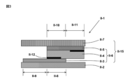
- FIG. 3 shows a cross-sectional view of a long laminate according to another embodiment (second aspect) of the present invention, taken along a direction perpendicular to the longitudinal direction.
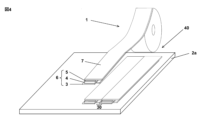
- FIG. 4 is a diagram showing a method for producing a photovoltaic device by sequentially attaching a plurality of power generating laminates provided in a long laminate according to an embodiment of the present invention to a device substrate.
- FIG. 1 is a perspective view of a long laminate according to an embodiment of the present invention.
- FIG. 2 shows a cross-sectional view of a long laminate according to one embodiment (first aspect) of the present invention in a direction perpendicular to the longitudinal direction.
- FIG. 3 shows a cross-sectional view of a long laminate according to
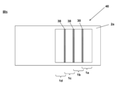
- FIG. 5 shows a plan view of a photovoltaic device of the present invention, which is obtained by sequentially attaching a plurality of power generating laminates provided in a long laminate according to an embodiment of the present invention to a device substrate.
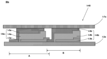
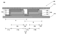
- FIG. 6 shows an example of a cross-sectional view of a photovoltaic device according to one embodiment (first aspect) of the present invention.
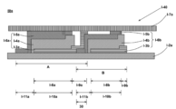
- FIG. 7 shows another example of a cross-sectional view of a photovoltaic device according to one embodiment (first aspect) of the present invention.
- FIG. 8 shows yet another example of a cross-sectional view of a photovoltaic device according to one embodiment (first aspect) of the present invention.
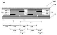
- FIG. 9 shows an example of a cross-sectional view of a photovoltaic device according to another embodiment (second aspect) of the present invention.
- the present invention includes a long laminate, a photovoltaic device, and a method for manufacturing a photovoltaic device of a first embodiment, and a long laminate, a photovoltaic device, and a method for manufacturing a photovoltaic device of a second embodiment.
- a long laminate, a photovoltaic device, and a method for manufacturing a photovoltaic device of a second embodiment are mentioned.
- the reference numerals in the drawings relating to the first embodiment are expressed as a combination of I and a number (e.g., I-1)
- the reference numerals in the drawings relating to the second embodiment are expressed as a combination of II and a number (e.g., II-1)
- the reference numerals in the drawings relating to both the first and second embodiments may be expressed only in Arabic numerals, omitting the Roman numerals.
- Figure 1 shows a perspective view of a long laminate according to an embodiment of the present invention
- Figure 2 shows a cross-sectional view of a long laminate according to one embodiment of the present invention (first aspect) in a direction perpendicular to the longitudinal direction
- Figure 3 shows a cross-sectional view of a long laminate according to another embodiment of the present invention (second aspect) in a direction perpendicular to the longitudinal direction.
- the long laminate 1 (I-1, II-1) includes a base layer 2 (I-2, II-2) having a width direction and a length direction, and a laminate 6 (I-6, II-6) formed on the base layer (I-2, II-2).
- the laminate 6 (I-6, II-6) includes a first electrode 3 (I-3, II-3) formed on the base layer 2 (I-2, II-2), a photovoltaic layer 4 (I-4, II-4) at least partially formed on the first electrode 3 (I-3, II-3), and a second electrode 5 (I-5, II-5) at least partially formed on the photovoltaic layer 4 (I-4, II-4), and has a power generation function.
- the second electrode 5 (I-5, II-5) has a 2-1 region 10 (I-10, II-10) facing the first electrode 3 (I-3, II-3) and a 2-2 region 11 not facing the first electrode 3 (I-3, II-3), and the 2-2 region 11 is present on one widthwise side of the base layer 2 (I-2, II-2) but not on the other widthwise side of the base layer 2 (I-2, II-2).
- the long laminate 1 (I-1, II-1) is wound, for example, in a reel shape. Furthermore, the long laminate 1 (I-1, II-1) may have a protective layer 7 (I-7, II-7) on the second electrode 5 (I-5, II-5).
- the width direction of the configuration is described as being substantially parallel to the width direction of the base layer
- the length direction of the configuration is described as being substantially parallel to the length direction of the base layer.
- this description is merely for convenience, and the length of a certain configuration in these two directions can be changed as appropriate within a range that does not impair the effect, and there may be cases where the direction described as the length direction is the short direction.
- the second electrode I-5 is formed on the photovoltaic layer I-4, and is preferably also formed on the side surface of the photovoltaic layer I-4 and on the base layer I-2.
- the second electrode II-5 is preferably formed only on the photovoltaic layer II-4, and one widthwise side of the photovoltaic layer II-4 is preferably formed on the first electrode II-3, and the other widthwise side of the photovoltaic layer II-4 is preferably not formed on the first electrode II-3.
- the long laminate 1 has a predetermined size in the thickness direction, width direction, and length (longitudinal) direction.
- the longitudinal size of the long laminate 1 may be longer than the transverse size, and is preferably 6 cm to 100 m, more preferably 10 cm to 80 m, and even more preferably 15 cm to 50 m.
- the size in the width direction of the long laminate 1 is preferably 1 cm or more and 100 cm or less, more preferably 2 cm or more and 80 cm or less, even more preferably 5 cm or more and 60 cm or less, and even more preferably 10 cm or more and 40 cm or less.
- the size in the thickness direction of the long laminate 1 is preferably 1 ⁇ m or more and 10,000 ⁇ m or less, more preferably 2 ⁇ m or more and 8,000 ⁇ m or less, even more preferably 5 ⁇ m or more and 6,000 ⁇ m or less, and even more preferably 10 ⁇ m or more and 4,000 ⁇ m or less.
- the substrate layer 2 is not particularly limited as long as it has flexibility, heat resistance, and the like so that the first electrode 3, the photovoltaic layer 4, the second electrode 5, and the like can be formed thereon.
- Examples of materials constituting the substrate layer 2 include organic materials, metal materials, fabric materials, and paper materials.
- organic materials include olefin resins such as polyester resin, methacrylic resin, methacrylic-maleic acid copolymer resin, polystyrene resin, fluororesin, polyimide resin, fluorinated polyimide resin, polyamide resin, polyamideimide resin, polyetherimide resin, cellulose resin, polyurethane resin, polyether ether ketone resin, polycarbonate resin, alicyclic polyolefin resin, polyarylate resin, polyethersulfone resin, polysulfone resin, cycloolefin resin, polyethylene terephthalate resin, polyethylene naphthalate resin, polyethylene resin, and polypropylene resin; and vinyl resins such as polyvinyl chloride resin and polyvinyl alcohol resin.
- the metal material include aluminum and copper that have been given insulating properties.
- the fabric material include nonwoven fabric and net.
- the paper material may be paper or synthetic paper.
- the substrate layer 2 may be any of the above materials, or a combination of the above materials.
- One or more of the organic materials, metal materials, fabric materials, and paper materials may be used.
- the plastic film has a low water vapor transmission rate.
- the organic material may have a predetermined glass transition temperature as an index of a predetermined strength, and the glass transition temperature of the organic material is preferably 50°C or higher, more preferably 60°C or higher, and preferably 300°C or lower, more preferably 280°C or lower.
- the glass transition temperature can be calculated based on, for example, JIS K 7121.
- the shape of the base layer 2 may be any of a plate, a film, and a sheet.
- a curved structure may be formed in a part or all of the base material layer 2.
- the size in the thickness direction of the base layer 2 is, for example, 0.5 ⁇ m or more and 50 ⁇ m or less, preferably 1 ⁇ m or more and 20 ⁇ m or less, more preferably 2 ⁇ m or more and 10 ⁇ m or less, and further preferably 3 ⁇ m or more and 8 ⁇ m or less.
- the size of the base material layer 2 in the width direction and the length direction may be the same as the size of the long laminate 1 in the width direction and the length direction.
- the substrate layer 2 is preferably wound in a reel shape. As described above, when a plurality of laminates 6 are present along the longitudinal direction of the substrate layer 2, the substrate layer 2 is preferably wound in a reel shape along the longitudinal direction.
- the substrate layer 2 (I-2, II-2), the laminate 6 (I-6, II-6) (including the first electrode 3 (I-3, II-3), the photovoltaic layer 4 (I-4, II-4), and the second electrode 5 (I-5, II-5)) on the substrate layer 2 (I-2, II-2), and the protective layer 7 (I-7, II-7) may also be wound in a reel shape if provided.
- the long laminate 1 (I-1, II-1) wound in a reel shape in this manner is preferably formed into a film roll.
- a film roll for example, when the long laminate 1 includes a plurality of laminates 6, the long laminate 1 may be easily handled.
- the long laminate 1 (I-1, II-1) when it is described that the long laminate 1 (I-1, II-1) is wound in a reel shape, it is intended to include the case where the entire long laminate 1 (I-1, II-1) is wound in a reel shape, and the case where the long laminate 1 (I-1, II-1) is partially wound in a reel shape.
- the base material layer 2 is preferably in contact with the first electrode 3 via an adhesive layer,
- the base layer 2 is preferably peelable so that the laminate 6 including the first electrode 3, the photovoltaic layer 4, and the second electrode 5 can be attached to a desired object.
- peeling off the base layer 2 leaves the adhesive layer on the first electrode 3 side, for example, and the first electrode 3 etc. can be attached to a desired target by the adhesive force of the adhesive layer.
- the adhesive layer is partially provided or not provided on the portion of the first electrode 3 etc. that is used for electrical connection as described later. The same applies to the other adhesive layers described later.
- the adhesive layer itself may be a peelable layer, but a release layer may be provided separately from the adhesive layer.
- a release layer and an adhesive layer are provided in this order between the base layer 2 and the first electrode 3, when the base layer 2 is peeled off, for example, the adhesive layer remains on the first electrode 3 side, and the first electrode 3 etc. can be attached to a desired target by the adhesive force of the adhesive layer.
- Materials for the release layer include silicone-based materials and non-silicone-based materials (eg, acrylic-based materials, urethane-based materials).
- the stack 6 (I-6, II-6) includes a first electrode 3 (I-3, II-3), a photovoltaic layer 4 (I-4, II-4), and a second electrode 5 (I-5, II-5).
- a part of the photovoltaic layer 4 (I-4, II-4) is formed on the first electrode 3 (I-3, II-3)
- at least a part of the second electrode 5 (I-5, II-5) is formed on the photovoltaic layer 4 (I-4, II-4).
- the first electrode 3 (I-3, II-3), the photovoltaic layer 4 (I-4, II-4), and the second electrode 5 (I-5, II-5) may be laminated in this order, or other layers may be formed between the first electrode 3 (I-3, II-3) and the photovoltaic layer 4 (I-4, II-4) and between the photovoltaic layer 4 (I-4, II-4) and the second electrode 5 (I-5, II-5).
- the other layers are preferably a hole extraction layer, an electron extraction layer, an adhesive layer made of a conductive paste, or the like, as described below.
- the laminate 6 (I-6, II-6) including the first electrode 3 (I-3, II-3), the photovoltaic layer 4 (I-4, II-4), and the second electrode 5 (I-5, II-5) may be present in one layer along the longitudinal direction of the base layer 2 (I-2, II-2), or a plurality of layers may be present along the longitudinal direction of the base layer 2 (I-2, II-2). However, it is preferable that a plurality of layers are present along the longitudinal direction of the base layer 2 (I-2, II-2). When there are a plurality of laminates 6, it is preferable that there is an area where no laminate is formed between one laminate 6 and another laminate 6. Each laminate constitutes a cell unit due to the area. It is preferable that the plurality of laminates 6 have the same structure.
- the number of laminates 6 is preferably 2 to 1,000, more preferably 3 to 700, even more preferably 5 to 400, and even more preferably 10 to 100.
- the laminate 6 including the first electrode 3, the photovoltaic layer 4, and the second electrode 5 may exist in one piece in the width direction of the base layer 2, or may exist in multiple pieces in the width direction of the base layer 2.
- the width of the laminate 6 is, for example, 1 cm or more and 100 cm or less, preferably 2 cm or more and 80 cm or less, more preferably 5 cm or more and 60 cm or less, and further preferably 10 cm or more and 40 cm or less.
- the longitudinal size of the laminate 6 is, for example, 5 cm or more and 200 cm or less, preferably 10 cm or more and 150 cm or less, more preferably 15 cm or more and 100 cm or less, and even more preferably 20 cm or more and 80 cm or less.
- the size in the thickness direction of the laminate 6 is, for example, 30 nm or more and 3000 nm or less, preferably 60 nm or more and 2400 nm or less, more preferably 90 nm or more and 1800 nm or less, and further preferably 150 nm or more and 1200 nm or less.
- the first electrode 3 (I-3, II-3) formed on the base layer 2 preferably has a 1-1 region 8 (I-8, II-8) facing the second electrode 5 (I-5, II-5) and a 1-2 region 9 (I-9, II-9) not facing the second electrode 5 (I-5, II-5).
- the first electrode and the second electrode can be connected in a planar manner, and therefore the wiring resistance can be reduced.
- the 1-2 region 9 (I-9, II-9) of the first electrode may be a region in which the second electrode 5 (I-5, II-5) is not formed, or may be a region in which neither the photovoltaic layer 4 (I-4, II-4) nor the second electrode 5 (I-5, II-5) is formed.
- the 1-2 region 9 (I-9, II-9) of the first electrode is present on the other widthwise side of the base layer 2 (I-2, II-2) and not present on one widthwise side of the base layer 2 (I-2, II-2). That is, the 1-2 region 9 (I-9, II-9) of the first electrode does not exist on both sides of the 1-1 region 8 (I-8, II-8) (2-1 region 10 (I-10, II-10)) where the first electrode 3 (I-3, II-3) and the second electrode 5 (I-5, II-5) face each other, but preferably exists on one side of the 1-1 region 8 (I-8, II-8) (2-1 region 10 (I-10, II-10)).
- the first electrode 3 (I-3, II-3), more specifically, the 1-2 region 9 (I-9, II-9) of the first electrode 3 (I-3, II-3) has a portion where no other layers are provided between the first electrode 3 (I-3, II-3) (which can be read as the 1-2 region 9 (I-9, II-9)) and the height at which the second electrode 5 (I-5, II-5) is provided on the photovoltaic layer 4 (I-4, II-4). In the example of Figures 2 and 3, this portion is provided at the end of the first electrode 3 (I-3, II-3).
- the 1-1 region 8 is preferably larger than the 1-2 region 9 . That is, when the total length (based on the width direction length) of the 1-1 region 8 and the 1-2 region 9 of the first electrode 3 is taken as 100%, the length ratio of the 1-1 region 8 is preferably more than 50% and not more than 90%, more preferably 60% or more and not more than 85%, and further preferably 65% or more and not more than 80%. With such a length ratio, the inflow and outflow of electrons can be performed successfully in the electrode.
- the length ratio of the 1-2 region 9 is preferably 10% or more and less than 50%, more preferably 15% or more and 40% or less, and even more preferably 20% or more and 35% or less.
- the 1-2 region 9 of the first electrode 3 satisfies the length ratio in the above range, by bonding it to another laminate as described below, a part (overlapping part) electrically connected with the second electrode or photovoltaic layer of the other laminate is formed, so that a plurality of laminates can be connected in series.
- the laminate having a power generating function can be adapted to the shape and size of the device, and it is possible to maximize the power generating area relative to the total area of the laminate having a power generating function provided in the device.
- the wiring resistance can be reduced.
- the second electrode 5 (I-5, II-5) is at least partially formed on the photovoltaic layer 4 (I-4, II-4).
- the second electrode I-5 is preferably formed not only on the photovoltaic layer I-4 but also on the side surface of the photovoltaic layer I-4 and the base layer I-2.
- the second electrode I-5 has a portion (a 2-2z region I-11z described later) that extends on the base layer I-2 via the side surface of the photovoltaic layer I-4.
- the second electrode II-5 is preferably formed only on the photovoltaic layer II-4.
- the 2-1 region 10 and the 2-2 region 11 of the second electrode 5 will be described below. Similar to the 1-1 region 8 of the first electrode 3, the 2-1 region 10 of the second electrode 5 corresponds to the region where the first electrode 3 and the second electrode 5 face each other.
- the second-2 region 11 (I-11, II-11) of the second electrode 5 (I-5, II-5) is not opposed to the first electrode 3 (I-3, II-3), is present on one widthwise side of the base layer 2 (I-2, II-2), and is not present on the other widthwise side of the base layer 2 (I-2, II-2). It is preferable that the second-2 region 11 (I-11, II-11) is a region that is formed only on one widthwise side of the base layer 2 (I-2, II-2).
- the 2-2 region I-11 may include a 2-2x region I-11x (the region surrounded by I-11xl and I-11xh in FIG. 2) provided on the photovoltaic layer I-4, a 2-2y region I-11y (the region surrounded by I-11yl and I-11yh in FIG. 2) provided on the side surface of the photovoltaic layer I-4, and a 2-2z region I-11z (the region surrounded by I-11zl and I-11zh in FIG. 2) provided on the base layer I-2.
- the 2-2y region I-11y is preferably in contact with the side surface of the photovoltaic layer I-4, and preferably connects the 2-2x region I-11x and the 2-2z region I-11z.
- the 2-2z region I-11z of the second electrode 5 (I-5), more specifically the 2-2z region I-11z of the 2-2 region I-11 of the second electrode 5 (I-5), is the portion that extends on the base layer I-2 via the side of the photovoltaic layer I-4, and is a portion where no other layer is provided between the portion and the height at which the second electrode 5 (I-5) is provided on the photovoltaic layer I-4. In the example of FIG. 2, the portion is provided at the end of the second electrode 5 (I-5).
- the side surface of the photovoltaic layer I-4 may have a slope (e.g., greater than 0 degrees and less than or equal to 90 degrees) with respect to the lower surface of the photovoltaic layer I-4, and when the slope is 90 degrees, the side surface may be perpendicular to the upper and lower surfaces of the photovoltaic layer I-4.
- a slope e.g., greater than 0 degrees and less than or equal to 90 degrees
- the second-2y region I-11y provided on the side surface of the photovoltaic layer I-4 may form a shape such as a rectangle or a parallelogram, and the upper and lower surfaces of the second electrode I-5 constituting the second-2y region I-11y may have a gradient start point and a gradient end point, or may form a gradient surface (the gradient is, for example, greater than 0 degrees and less than or equal to 90 degrees, based on the upper surface of the base material layer I-2).
- the gradient start point may be a point closer to substrate layer I-2, and the gradient end point may be a point farther from substrate layer I-2.
- I-11xl may be, for example, the length of a line segment connecting a junction between the lower surface of the second electrode I-5 and the upper surface of the photovoltaic layer I-4 and a junction between the upper surface of the photovoltaic layer I-4 and a side surface of the photovoltaic layer I-4, which corresponds to a junction between the 2-1 region I-10 and the 2-2 region I-11 of the second electrode I-5.
- I-11yl may be, for example, the length of a line segment connecting a junction between the upper surface of the photovoltaic layer I-4 and a side surface of the photovoltaic layer I-4 and a junction between a plane parallel to the upper surface of the photovoltaic layer I-4 and a gradient surface derived from the upper surface of the second electrode I-5 (or a length corresponding to the size of the second electrode I-5 in the thickness direction).
- I-11yl may be, for example, the length of a line segment connecting two points obtained by projecting the gradient start point and gradient end point of the upper surface of the second electrode I-5 onto the upper surface of the base material layer I-2.
- I-11zl may be, for example, the length of a line segment connecting an end point of the upper surface of the second electrode I-5 corresponding to the end point of the 2-2 region I-11 and the gradient starting point of the upper surface of the second electrode I-5.
- I-11xh may be, for example, a height corresponding to the size of the second electrode I-5 in the thickness direction.
- I-11yh may be, for example, a height corresponding to the size in the thickness direction of a stack I-6 composed of a first electrode I-3, a photovoltaic layer I-4, and a second electrode I-5.
- I-11zh may be, for example, a height corresponding to the size in the thickness direction of the first electrode I-3 and/or the second electrode I-5.
- the lengths (based on the width direction length) of the 2-2x region I-11x, the 2-2y region I-11y, and the 2-2z region I-11z have the following relationship: length of the 2-2x region I-11x (I-11xl in FIG. 2) ⁇ length of the 2-2y region I-11y (I-11yl in FIG. 2) ⁇ length of the 2-2z region I-11z (I-11zl in FIG. 2).
- the thicknesses of the second-1 region I-10 and the second-2 region I-11 preferably have the relationship: thickness of the second-1 region I-10 ⁇ thickness of the second-2 region I-11.
- the thicknesses of the 2-2x region I-11x, the 2-2y region I-11y, and the 2-2z region I-11z satisfy the following relationship: thickness of the 2-2z region I-11z (I-11zh in FIG. 2) ⁇ thickness of the 2-2x region I-11x (I-11xh in FIG. 2) ⁇ thickness of the 2-2y region I-11y (I-11yh in FIG. 2).
- the second-2 region 11 (I-11, II-11) of the second electrode 5 does not exist on both sides of the second-1 region 10 (I-10, II-10) (1-1 region 8 (I-8, II-8)) where the first electrode 3 (I-3, II-3) and the second electrode 5 (I-5, II-5) face each other, but preferably exists on one side of the second-1 region 10 (I-10, II-10) (1-1 region 8 (I-8, II-8)).
- the laminate having a power generating function can be adapted to the shape and size of the device, and it is possible to maximize the power generating area relative to the total area of the laminate having a power generating function provided in the device.
- the first electrode and the second electrode can be connected in a planar manner, so that the wiring resistance can be reduced.
- the respective length ratios of the 2-1 region 10 and the 2-2 region 11 are as follows:
- the 2-1 region I-10 of the second electrode I-5 preferably has a longer length than the 2-1 region I-10 or the 2-2 region I-11, from the viewpoint of flowing electrons in or out of the photovoltaic layer.
- the length ratio of the 2-1 region I-10 of the second electrode I-5 is preferably 45% or more and 80% or less, more preferably 50% or more and 75% or less, and even more preferably 55% or more and 70% or less, when the total length (based on the width direction length) of the 2-1 region I-10 and the 2-2 region I-11 of the second electrode I-5 is 100%. If the length ratio is 45% or more, the flow of electrons into or out of the photovoltaic layer can be made successful, whereas if the length ratio is 80% or less, the length corresponding to the 2-2 region can be ensured.
- the 2-2 region I-11 of the second electrode I-5 is formed in the width direction of the base material layer, and may have a length shorter than the length of the 2-1 region I-10 from the viewpoint of ensuring a bonding portion with another laminate.
- the length ratio of the 2-2 region I-11 of the second electrode I-5 is preferably 20% or more and 55% or less, more preferably 25% or more and 50% or less, and even more preferably 30% or more and 45% or less, when the total length (based on the width direction length) of the 2-1 region I-10 and the 2-2 region I-11 of the second electrode I-5 is 100%. If the length ratio is 20% or more, it is easy to ensure a bonding portion with another laminate, while if the length ratio is 55% or less, the flow of electrons into or out of the photovoltaic layer can be successfully achieved.
- the 2-2 region I-11 of the second electrode I-5 satisfies the length ratio in the above range, by bonding it with another laminate, a part (overlapping part) electrically connected with the first electrode or photovoltaic layer 4 of the other laminate is formed, so that a plurality of laminates having a power generation function can be connected in series.
- the laminate having a power generation function is produced, it can be adapted to the shape and size of the device, and it is possible to maximize the power generation area relative to the total area of the laminate having a power generation function provided in the device.
- the wiring resistance can be reduced.
- the durability of the photovoltaic device can be increased by functioning stably for a long period of time even if it is deformed by the application of an external force.
- the photovoltaic layer II-4 has a portion that is provided below the second electrode II-5, more specifically, the second-2 region II-11, and has a portion below which no electrode exists. In the example of FIG. 3, this portion is provided at the end of the photovoltaic layer II-4. This makes it possible to form multiple stacks connected in series by overlapping and contacting this portion with the electrode of another stack during the manufacture of the photovoltaic device described below.
- the 2-2 region II-11 of the second electrode II-5 may have a length longer than the length of the 2-1 region II-10 from the viewpoint of ensuring a bonding portion with another laminate.
- the length ratio of the 2-2 region II-11 of the second electrode II-5 is preferably 45% or more and 80% or less, more preferably 50% or more and 75% or less, and even more preferably 55% or more and 70% or less, when the total length (based on the width direction length) of the 2-1 region II-10 and the 2-2 region II-11 of the second electrode II-5 is 100%.
- the length ratio of the 2-1 region II-10 of the second electrode II-5 is preferably 20% or more and 55% or less, more preferably 25% or more and 50% or less, and even more preferably 30% or more and 45% or less, when the total length (based on the width direction length) of the 2-1 region II-10 and the 2-2 region II-11 of the second electrode II-5 is 100%.
- the length ratio is 20% or more, the strength of the laminate is easily ensured, whereas when the length ratio is 55% or less, the bonding portion with another laminate is easily ensured.
- the 2-2 region 11 (I-11, II-11) of the second electrode 5 (I-5, II-5) and the 1-2 region 9 (I-9, II-9) of the first electrode 3 (I-3, II-3) are present on one side and the other side in the width direction of the base layer 2 (I-2, II-2), respectively.
- the 2-2 region 11 of the second electrode 5 and the 1-2 region 9 of the first electrode 3 may have the same length or may have different lengths.
- first electrode 3 and the second electrode 5 are a negative electrode (anode) and the other is a positive electrode (cathode). It is also preferable that at least the second electrode 5 has optical transparency, and it is more preferable that both the second electrode 5 and the first electrode 3 have optical transparency.
- Each of the first electrode 3 and the second electrode 5 may be a single layer made of a conductive material, or may have a laminated structure of two or more layers.
- the negative electrode is made of a conductive material with a high work function, and is an electrode through which electrons flow into an external circuit.
- materials constituting the negative electrode include metal oxides such as nickel oxide, tin oxide, indium oxide, indium tin oxide (ITO), indium zirconium oxide (IZO), titanium oxide, indium oxide, and zinc oxide; metals such as gold, platinum, silver, chromium, and cobalt, and alloys thereof.
- a conductive polymer material such as PEDOT:PSS in which a polythiophene derivative is doped with polystyrene sulfonic acid, or polypyrrole or polyaniline doped with iodine or the like may be used.
- a transparent electrode it is preferable to use a light-transmitting metal oxide such as ITO, zinc oxide, or tin oxide, and it is more preferable to use ITO.
- the size in the thickness direction of the first electrode or the second electrode that will be the negative electrode is, for example, 10 nm or more and 1000 nm or less, preferably 20 nm or more and 800 nm or less, more preferably 30 nm or more and 600 nm or less, and even more preferably 50 nm or more and 400 nm or less.
- the size in the thickness direction of the negative electrode is within this range, light can be efficiently converted into electricity without reducing the light transmittance.
- the width of the first or second electrode that is the negative electrode may be the same as or different from the width of the laminate 6.
- the electrode that is the negative electrode, either the first electrode or the second electrode may have a predetermined sheet resistance, and the value of the sheet resistance is, for example, 1 ⁇ / ⁇ or more and 1000 ⁇ / ⁇ or less, preferably 2 ⁇ / ⁇ or more and 500 ⁇ / ⁇ or less, and more preferably 5 ⁇ / ⁇ or more and 100 ⁇ / ⁇ or less.
- the negative electrode out of the first and second electrodes may be formed using a vacuum film-forming method such as vapor deposition or sputtering, or a wet coating method in which an ink containing nanoparticles or the like is applied to form a film, and may be etched or otherwise shaped as required.
- a vacuum film-forming method such as vapor deposition or sputtering, or a wet coating method in which an ink containing nanoparticles or the like is applied to form a film, and may be etched or otherwise shaped as required.
- the positive electrode is made of a conductive material having a low work function, and is an electrode into which electrons flow.
- materials constituting the positive electrode include metals such as platinum, gold, silver, copper, iron, tin, zinc, aluminum, indium, chromium, lithium, sodium, potassium, cesium, calcium, and magnesium, and alloys thereof; inorganic salts such as lithium fluoride and cesium fluoride; and metal oxides such as nickel oxide, aluminum oxide, lithium oxide, and cesium oxide.
- Preferred materials for forming the positive electrode are metals such as platinum, gold, silver, copper, iron, tin, aluminum, calcium, and indium, and alloys of such metals with indium tin oxide or the like.
- the size in the thickness direction of the electrode that will be the positive electrode, of the first electrode or the second electrode is, for example, 10 nm or more and 1000 nm or less, preferably 20 nm or more and 800 nm or less, more preferably 30 nm or more and 600 nm or less, and even more preferably 50 nm or more and 400 nm or less.
- the size in the thickness direction of the positive electrode is within this range, light can be efficiently converted into electricity without reducing the light transmittance.
- the width of the first or second electrode that is the positive electrode may be the same as or different from the width of the laminate 6.
- the electrode that is the positive electrode, either the first electrode or the second electrode may have a predetermined sheet resistance, and the value of the sheet resistance is, for example, 1 ⁇ / ⁇ or more and 1000 ⁇ / ⁇ or less, preferably 2 ⁇ / ⁇ or more and 500 ⁇ / ⁇ or less, and more preferably 5 ⁇ / ⁇ or more and 100 ⁇ / ⁇ or less.
- the electrode that is the positive electrode, either the first or second electrode may be formed using a vacuum film-forming method such as vapor deposition or sputtering, or a wet coating method in which an ink containing nanoparticles or the like is applied to form a film, and may be etched or otherwise shaped into a desired shape as necessary.
- a vacuum film-forming method such as vapor deposition or sputtering, or a wet coating method in which an ink containing nanoparticles or the like is applied to form a film, and may be etched or otherwise shaped into a desired shape as necessary.
- the negative and positive electrodes may each use one or more materials in each layer, may have a laminated structure of two or more layers, and other layers may be formed in the negative and positive electrodes.
- Materials used in the other layers may be poly(ethylenedioxythiophene):poly(styrenesulfonic acid) (PEDOT:PSS), molybdenum oxide, lithium fluoride, 2,9-dimethyl-4,7-diphenyl-1,10-phenanthroline, etc.
- At least one electrode preferably has optical transparency from the viewpoint of absorbing solar light, and it is more preferable that the electrode has an optical transmittance of preferably 40% or more, more preferably 55% or more, even more preferably 85% or more, and even more preferably 90% or more in the wavelength range of 360 to 830 nm.
- the electrode may be formed using any of the above metal oxides or alloys thereof.
- Photovoltaic Layer At least a portion of the photovoltaic layer 4 (I-4, II-4) is formed on the first electrode 3 (I-3, II-3).
- the photovoltaic layer I-4 may be formed not only on the first electrode I-3 but also on the base material layer I-2.
- Materials constituting the photovoltaic layer 4 include organic compound materials (e.g., organic dye materials, organic semiconductor materials), etc.
- the material constituting the photovoltaic layer 4 is preferably an organic semiconductor material from the viewpoints of light weight, flexibility, etc.
- the photovoltaic layer 4 preferably includes an organic thin film.
- organic dye material examples include dye-sensitizable coumarin derivatives, mercurochrome dyes, etc.
- Organic semiconductor materials are broadly divided into p-type and n-type, but because the holes and electrons that contribute to electrical conduction change depending on the electronic state, doping state, and trap state of the material, it is sometimes not possible to clearly classify them as p-type or n-type, and the same material may exhibit both p-type and n-type properties.
- the p-type semiconductor may be a polymer organic semiconductor compound, a low molecular weight organic semiconductor compound, or the like.
- the polymer organic semiconductor compound include conjugated polymer semiconductor compounds such as polythiophene, polyfluorene, polyphenylene vinylene, polythienylene vinylene, polyacetylene, and polyaniline; polymer semiconductor compounds such as substituted oligothiophenes; and semiconductor compounds obtained by copolymerizing two or more types of monomers.
- the polymeric organic semiconductor compound may be one type of compound or a mixture of multiple types of compounds.
- low molecular weight organic semiconductor compounds include condensed aromatic hydrocarbons such as naphthacene, pentacene, and pyrene; oligothiophenes containing four or more thiophene rings; compounds containing one or more selected from thiophene rings, benzene rings, fluorene rings, naphthalene rings, anthracene rings, thiazole rings, thiadiazole rings, and benzothiazole rings, with a total of four or more rings linked together; phthalocyanine compounds, metal complexes thereof, porphyrin compounds such as tetrabenzoporphyrin, and macrocyclic compounds such as metal complexes thereof, and the like.
- the molecular weight of the low molecular weight organic semiconductor compound is, for example, 100 or more and 5,000 or less, and preferably 200 or more and 2,000 or less.
- the photovoltaic layer 4 is not limited thereto.
- a material used in a silicon-based solar cell such as a crystalline silicon solar cell and an amorphous silicon solar cell
- a compound-based solar cell such as a CIS solar cell, a CIGS solar cell, and a CdTe solar cell
- an organic-inorganic hybrid solar cell which may also be referred to as a perovskite solar cell
- a solar cell such as a dye-sensitized solar cell
- the material constituting the photovoltaic layer 4 for example, a silicon material, an inorganic compound material other than a silicon material, a perovskite material, and a quantum dot material may be used.
- the silicon material include single crystal silicon, polycrystalline silicon, microcrystalline silicon, and amorphous silicon.
- the inorganic compound material include InGaAs, GaAs, CIS, CIGS, CZTS, CdTe/CdS, InP, SiGe, Ge, and ZnO/CuAlO 2 . When such a material can be used, it is possible to form a thin layer, which is advantageous in terms of ease of handling during winding into a reel and transfer, which will be described later.
- n-type semiconductors include fullerene compounds, quinolinol derivative metal complexes such as 8-hydroxyquinoline aluminum, condensed ring tetracarboxylic acid diimides such as naphthalene tetracarboxylic acid diimide and perylene tetracarboxylic acid diimide, perylene diimide derivatives, terpyridine metal complexes, tropolone metal complexes, flavonol metal complexes, perinone derivatives, benzimidazole derivatives, benzoxazole derivatives, thiazole derivatives, benzthiazole derivatives, benzothiadiazole derivatives, oxadiazole derivatives, thiadiazole derivatives, triazole derivatives, pyrazine derivatives, phenanthroline derivatives, quinoxaline derivatives, benzoquinoline derivatives, borane derivatives, fluorides of condensed polycyclic aromatic hydrocarbons such as anthracene, pyrene
- the photovoltaic layer 4 may include at least a p-type semiconductor and an n-type semiconductor.
- the photovoltaic layer 4 may be a single layer, or may be configured as a laminated structure of two or more layers.
- the photovoltaic layer 4 may contain, for example, an n-type semiconductor and a p-type semiconductor in separate layers, or may contain an n-type semiconductor and a p-type semiconductor in the same layer.
- the n-type semiconductor and the p-type semiconductor used in the photovoltaic layer 4 may each be used alone or in combination of two or more kinds.
- Examples of the configuration of the photovoltaic layer 4 include a bulk heterojunction type having a layer (i layer) in which a p-type semiconductor and an n-type semiconductor are separated within the layer, a stacked type (hetero pn junction type) in which a layer containing a p-type semiconductor (p layer) and a layer containing an n-type semiconductor (n layer) have an interface, a Schottky type, and combinations of these.
- the size in the thickness direction of the photovoltaic layer 4 is, for example, 10 nm or more and 1000 nm or less, preferably 20 nm or more and 500 nm or less, and more preferably 50 nm or more and 300 nm or less.
- the size of the photovoltaic layer 4 in the width direction is smaller than the size of the laminate 6 in the width direction, for example.
- the photovoltaic layer 4 is preferably formed by a coating method, and more preferably by a wet coating method.
- the coating method include spin coating, reverse roll coating, gravure coating, kiss coating, spray coating, air knife coating, impregnation coating, and curtain coating.
- Electron Transport Layer An electron transport layer (electron transport layer II-12 in the example of FIG. 3) may be provided between the photovoltaic layer 4 and the electrode. The electron transport layer extracts electrons generated in the photovoltaic layer 4 and acts as an energy barrier to holes.
- the material constituting the electron transport layer may be any material as long as it is a material through which electrons can easily move, and examples of such materials include organic materials such as cyano group-containing polyphenylene vinylene, oxadiazole compounds, benzimidazole compounds, naphthalene tetracarboxylic acid compounds, perylene derivatives, and fluoro group-containing phthalocyanines, and inorganic materials such as phosphine oxide compounds, phosphine sulfide compounds, titanium oxide, zinc oxide, indium oxide, tin oxide, gallium oxide, tin sulfide, indium sulfide, and zinc sulfide.
- organic materials such as cyano group-containing polyphenylene vinylene, oxadiazole compounds, benzimidazole compounds, naphthalene tetracarboxylic acid compounds, perylene derivatives, and fluoro group-containing phthalocyanines
- inorganic materials such as
- the size of the electron transport layer in the thickness direction is, for example, 1 nm or more and 300 nm or less, preferably 2 nm or more and 200 nm or less, and more preferably 5 nm or more and 100 nm or less.
- the long laminate II-1 of the second embodiment preferably has an electron transport layer II-12 between the first electrode II-3 and the photovoltaic layer II-4 and/or between the second electrode II-5 and the photovoltaic layer II-4.
- the long laminate II-1 has an electron transport layer II-12 between the 1-1 region II-8 of the first electrode II-3 and the photovoltaic layer II-4, and has another electron transport layer II-12 between the 2-2 region II-11 of the second electrode II-5 and the photovoltaic layer II-4.
- the long laminate II-1 may have an electron transport layer II-12 between the 2-1 region II-10 of the second electrode II-5 and the photovoltaic layer II-4, and another electron transport layer II-12 below the 2-2 region II-11 of the second electrode II-5 and in contact with the lower surface of the photovoltaic layer II-4.
- the long laminate 1 (I-1, II-1) preferably further has a protective layer 7 (I-7, II-7) on the second electrode 5 (I-5, II-5).
- the protective layer 7 is preferably a layer that prevents deterioration of the laminate 6 from corrosion due to temperature, humidity, natural light, wind and rain, etc.
- Materials for the protective layer 7 include polyethylene resin, polypropylene resin, cyclic olefin resin, acrylonitrile-styrene resin, acrylonitrile-butadiene-styrene resin, polyvinyl chloride resin, fluororesin, polyester resins such as polyethylene terephthalate resin and polyethylene naphthalate resin, phenol resin, polyacrylic resin, polyamide resin, polyimide resin, polyurethane resin, silicone resin, etc.
- the protective layer 7 is weather resistant, it is preferable that the protective layer 7 is a fluororesin.
- fluororesins include polytetrafluoroethylene, 4-fluoroethylene-perchloroalkoxy copolymer, 4-fluoroethylene-6-fluoropropylene copolymer, 2-ethylene-4-fluoroethylene copolymer, polyvinylidene fluoride, polyvinyl fluoride, etc.
- the protective layer 7 may be made of one type of material, or may be made of two or more types of materials.
- the protective layer 7 may be one layer or two or more layers.
- the size in the thickness direction of the protective layer 7 is, for example, 0.5 ⁇ m to 100 ⁇ m, preferably 1 ⁇ m to 50 ⁇ m, and more preferably 2 ⁇ m to 30 ⁇ m. As the size in the thickness direction of the protective layer is reduced, the flexibility is increased.
- the size of the protective layer 7 in the width direction and the length direction may be the same as the size of the long laminate 1 in the width direction and the length direction.
- the protective layer 7 is preferably transparent to visible light.
- the light transmittance of the protective layer 7 in the visible light range of wavelengths from 360 to 830 nm is preferably 80% or more, more preferably 90% or more, and even more preferably 95% or more.
- the protective layer 7 may be formed on the second electrode 5 via an adhesive layer, similar to the base layer 2.
- the protective layer 7 may be peelable, similar to the base layer 2.
- a desired target such as a barrier layer
- the protective layer 7 may be provided for each laminate, or one protective layer 7 may be provided above the plurality of laminates.
- the adhesive layer provided on the protective layer 7 may be a peelable layer, or a peeling layer may be provided separately from the adhesive layer.
- a peeling layer and an adhesive layer are provided in this order between the protective layer 7 and the second electrode 5, when the protective layer 7 is peeled off, for example, the adhesive layer remains on the second electrode 5 side, and a desired object (such as a barrier layer) can be attached to the second electrode 5 or the like due to the adhesive force of the adhesive layer.
- a desired object such as a barrier layer
- peeling off of the protective layer 7 can be facilitated.
- the peeling force when peeling the base layer 2 from the first electrode 3 and the peeling force when peeling the protective layer 7 from the second electrode 5 are preferably different from each other. Such peeling force is derived from the adhesive layer and/or peeling layer described above.
- the peeling force when peeling the protective layer 7 from the second electrode 5 is preferably greater than the peeling force when peeling the base layer 2 from the first electrode 3. This makes it easier for the base layer 2 to be peeled off before the protective layer 7, and the first electrode 3 and the like can be attached to the target in a state in which the protective layer 7 is not peeled off.
- the case in which the base layer 2 is peeled off when attaching to the attachment target will mainly be described, but the protective layer 7 may be peeled off instead of the base layer 2 when attaching to the attachment target.
- the peeling force when peeling the base layer 2 from the first electrode 3 is preferably greater than the peeling force when peeling the protective layer 7 from the second electrode 5. This makes it easier for the protective layer 7 to be peeled off before the base layer 2.
- the electrode that is present on the outside after attachment to an object is preferably a transparent electrode.
- the protective layer 7 and the base layer 2 may have a predetermined rigidity (e.g., bending rigidity), and it is preferable that the protective layer 7 and the base layer 2 have different rigidities, and it is more preferable that the rigidity of the protective layer 7 is greater than the rigidity of the base layer 2. This makes it easier to wind the long laminate 1 into a reel.
- a predetermined rigidity e.g., bending rigidity
- the long laminate 1 preferably includes a laminate 6 including a first electrode 3, a photovoltaic layer 4, and a second electrode 5, and further includes an area where the laminate 6 is not formed.
- the area where the laminate 6 is not formed includes an area where the first electrode 3, the photovoltaic layer 4, and the second electrode 5 are not formed on the base layer 2, an area where the photovoltaic layer 4 and the second electrode 5 are not formed on the first electrode 3, an area where the second electrode 5 is not formed on the photovoltaic layer 4, and an air gap area formed between the second electrode 5 and the protective layer 7.
- Such an area can be used when the multiple laminates provided in the long laminate 1 are attached to the device base material with some overlapping each other to form a photovoltaic device described later.
- the proportion of this region is 60% or more, the strength of the photovoltaic device itself can be easily ensured, and when the proportion of this region is 95% or less, a region for arranging the laminates in series can be easily ensured.
- the insulating layer In order to increase the power generation area relative to the total area of the power generating laminate provided in the device, it is desirable to reduce the area of the insulating layer that is irradiated with light relative to the light receiving surface of the device.
- the area of the insulating layer is preferably 10% or less, more preferably 5% or less, even more preferably 1% or less, and even more preferably 0% relative to 100% of the area of the long laminate.
- the long laminate does not include an insulating layer.
- the insulating layer does not have to be provided between each of the laminates arranged in series, but can be provided at any location as long as it ensures insulation between the first electrodes and second electrodes of each laminate.
- FIG. 4 is a diagram showing a method for producing a photovoltaic device by sequentially attaching a plurality of laminates 6 provided in a long laminate 1 according to an embodiment of the present invention to a device substrate
- Fig. 5 is a plan view of a photovoltaic device obtained by sequentially attaching a plurality of laminates 6 (preferably laminates 6 from which the substrate layer 2 has been peeled off) provided in a long laminate 1 to a device substrate.
- Fig. 6 shows an example of a cross-sectional view of a photovoltaic device according to one embodiment of the present invention (first aspect), and Figs.
- FIG. 7 and 8 show other examples of cross-sectional views of a photovoltaic device according to one embodiment of the present invention (first aspect).
- Fig. 9 shows an example of a cross-sectional view of a photovoltaic device according to another embodiment of the present invention (second aspect).
- the long laminate 1 is formed by arranging a plurality of laminates 6 (including a first electrode 3, a photovoltaic layer 4, and a second electrode 5 in this order) having the same structure along the longitudinal direction.
- the base layer 2 is peeled off from the long laminate 1 so as to expose at least the first electrode 3 of the first laminate of the plurality of laminates 6, and the exposed first electrode 3 surface is attached to the device substrate 2a to form the first laminate on the device substrate 2a.
- the base layer 2 is peeled off from the long laminate 1 so as to expose at least the first electrode 3 of the second laminate of the plurality of laminates 6, for example, the second laminate arranged next to the first laminate.
- first electrodes 3 of the first and second laminates are exposed by peeling off the base layer 2 once, this second peeling is not essential.
- the exposed first electrode 3 surface of the second laminate is attached to the device substrate 2a so as to be parallel to the long side of the first laminate and overlap the first laminate to form an overlapping portion 30.
- This specification mainly describes an example in which the photovoltaic device 40 is produced as described above from multiple laminates 6 arranged on the same long laminate 1, but for example, a photovoltaic device 40 having a similar structure to that described above may be produced by attaching the laminates 6 arranged on different long laminates 1 to the same device substrate 2a.
- the photovoltaic device 40 will be described with reference to Fig. 5.
- the photovoltaic device 40 uses a plurality of laminates 6 (preferably laminates 6 from which the base layer 2 has been peeled off) provided on the long laminate 1, and is produced by bonding the first, second, third, and fourth laminates (in Fig. 5, the reference characters 1a, 1b, 1c, and 1d are given in order of appearance) of the plurality of laminates 6 to the device base material 2a so that adjacent laminates partially overlap each other.
- the overlapping portion 30 between the laminates 1a, 1b, 1c, and 1d is a portion where the first electrode I-3 of a certain laminate overlaps with the second electrode 1-5 of another laminate to realize an electrical connection
- the second embodiment it is a portion where the first electrode II-3 of a certain laminate overlaps with the photovoltaic layer II-4 of another laminate to realize an electrical connection. That is, in the photovoltaic device 40, the plurality of laminates 6 arranged on the long laminate 1 are transferred onto the device substrate 2a and electrically connected.
- the photovoltaic device I-40 of the first embodiment will be described with reference to FIG. 6.
- the photovoltaic device I-40 includes a device substrate I-2a, a first laminate I-6a, and a second laminate I-6b.
- the first laminate I-6a includes a first electrode I-3a at least partially formed on the device substrate I-2a, a photovoltaic layer I-4a at least partially formed on the first electrode I-3a, and a second electrode I-5a at least partially formed on the photovoltaic layer I-4a.
- the second laminate I-6b includes a first electrode I-3b at least partially formed on the device substrate I-2a, a photovoltaic layer I-4b at least partially formed on the first electrode I-3b, and a second electrode I-5b at least partially formed on the photovoltaic layer I-4b.
- a first laminate I-6a and a second laminate I-6b are formed side by side on a device substrate I-2a.
- the configuration of the photovoltaic device I-40 will be described in detail with reference to FIG.
- the second electrode I-5a of the first laminate I-6a has a 2-1 region I-10a facing the first electrode I-3a of the first laminate I-6a and a 2-2 region I-11a not facing the first electrode I-3a of the first laminate I-6a.
- the second electrode I-5b of the second laminate I-6b has a 2-1 region I-10b facing the first electrode I-3b of the second laminate I-6b and a 2-2 region I-11b not facing the first electrode I-3b of the second laminate I-6b.
- the first electrode I-3a of the first laminate I-6a has a 1-1 region I-8a facing the second electrode I-5a of the first laminate I-6a and a 1-2 region I-9a not facing the second electrode I-5a.
- the first electrode I-3b of the second laminate I-6b has a 1-1 region I-8b facing the second electrode I-5b of the first laminate I-6b and a 1-2 region I-9b not facing the second electrode I-5b.
- the 1-2 region I-9a of the first electrode I-3a of the first laminate I-6a is stacked on and electrically connected to the 2-2 region I-11b of the second electrode I-5b of the second laminate I-6b (in FIG. 6, the first laminate I-6a corresponds to laminate A, and the second laminate I-6b corresponds to laminate B).
- the laminate having a power generating function can be adapted to the shape and size of the device, and the power generating area relative to the total area of the laminate having a power generating function provided in the device can be maximized.
- the first electrode and the second electrode can be connected in a planar manner, the wiring resistance can be reduced.
- the overlapping portions of the 1-2 region I-9a of the first electrode I-3a of the first laminate I-6a and the 2-2 region I-11b of the second electrode I-5b of the second laminate I-6b have a portion where no other layer is provided between the overlapping portion and the height at which the second electrodes 1-5a and 1-5b are provided on the photovoltaic layers 1-4a and 1-4b. Furthermore, in the example of FIG. 7 and FIG.
- the second electrode I-5a is a portion that extends on the base layer I-2a via the side surface of the photovoltaic layer I-4a, and has a portion where no other layer is provided between the overlapping portion and the height at which the second electrode I-5a is provided on the photovoltaic layer I-4a.
- This portion corresponds to the above-mentioned 2-2z region I-11z of the 2-2 region I-11a of the second electrode I-5a.
- the photovoltaic device II-40 includes a device substrate II-2a, a first laminate II-6a, and a second laminate II-6b.
- the first laminate II-6a includes a first electrode II-3a at least partially formed on the device substrate II-2a, a photovoltaic layer II-4a at least partially formed on the first electrode II-3a, and a second electrode II-5a at least partially formed on the photovoltaic layer II-4a.
- the second laminate II-6b includes a first electrode II-3b at least partially formed on the device substrate II-2a, a photovoltaic layer II-4b at least partially formed on the first electrode II-3b, and a second electrode II-5b at least partially formed on the photovoltaic layer II-4b.
- the first laminate II-6a and the second laminate II-6b are formed side by side on the device substrate II-2a, and in a cross section in the direction in which the first laminate II-6a and the second laminate II-6b are arranged, the width direction sizes of the first laminate II-6a and the second laminate II-6b (the width direction sizes when the first electrode II-3a, the photovoltaic layer II-4a, and the second electrode II-5a are projected onto the device substrate II-2a, and the width direction sizes when the first electrode II-3b, the photovoltaic layer II-4b, and the second electrode II-5b are projected onto the device substrate II-2a) are
- the ratio of the area occupied by the first electrode II-3a and the first electrode II-3b, the photovoltaic layer II-4a and the photovoltaic layer II-4b, and the second electrode II-5a and the second electrode II-5b to the area multiplied by the thickness direction size of the stacked body II-6a or the stacked body II-6b is, for example, 60% or
- the second electrode II-5b of the second stacked body II-6b has a second-1 region II-10b facing the first electrode II-3b of the second stacked body II-6b and a second-2 region II-11b not facing the first electrode II-3b of the second stacked body II-6b.
- the first electrode II-3a of the first stack II-6a has a 1-1 region II-8a facing the second electrode II-5a of the first stack II-6a and a 1-2 region II-9a not facing the second electrode I-5a.
- the first electrode II-3b of the second stack II-6b has a 1-1 region II-8b facing the second electrode II-5b of the first stack II-6b and a 1-2 region II-9b not facing the second electrode II-5b.
- the photovoltaic layer II-4a of the first stack II-6a is stacked on and electrically connected to the 1-2 region II-9b of the first electrode II-3b of the second stack II-6b (in FIG. 9, the first stack II-6a corresponds to stack A, and the second stack II-6b corresponds to stack B).
- the photovoltaic layer II-4a of the first stack II-6a has a portion that is provided below the 2-2 region II-11a of the second electrode II-5a of the first stack II-6a and is overlapped on and electrically connected to the 1-2 region II-9b of the first electrode II-3b of the second stack II-6b, and the 1-2 region II-9b of the first electrode II-3b of the second stack II-6b has a portion between the portion where the photovoltaic layer II-4a is overlapped and the 1-1 region II-8b of the first electrode II-3b of the second stack II-6b, where no other layer is provided above the first electrode II-3b up to the height where the second electrode II-5b is provided on the photovoltaic layer II-4b of the second stack II-6b.
- the first electrode II-3a more specifically, the 1-2 region II-9a of the first electrode II-3a has a portion where no other layer is provided between the first electrode II-3a (which can be read as the 1-2 region II-9a) and the height at which the second electrode II-5a is provided on the photovoltaic layer II-4a.
- this configuration it is possible to form further series connections by overlapping and contacting the electrodes of other stacks with this portion.
- the 1-1 region 8a, the 1-2 region 9a, the 2-1 region 10a, and the 2-2 region 11a are based on a relative relationship (opposing relationship) between the first electrode 3a and the second electrode 5a included in the first stacked body 6a
- the 1-1 region 8b, the 1-2 region 9b, the 2-1 region 10b, and the 2-2 region 11b are based on the relative relationship (opposing relationship) between the first electrode 3b and the second electrode 5b included in the second laminate 6b, and these regions are named based on the relative relationship (opposing relationship) between the first electrode and the second electrode included in each laminate.
- the electrically connected region preferably corresponds to the overlapping portion 30 shown in FIG. 5.
- a plurality of laminates having a power generating function can be attached to a device substrate to connect the plurality of laminates in series.
- the first electrode and the second electrode can be connected in a planar manner, thereby reducing the wiring resistance.
- the overlapping portion has a certain area, it functions stably for a long period of time even if it is deformed by the application of an external force, thereby increasing the durability of the photovoltaic device.
- the electrically connected region means that the first electrode I-3a of the first laminate I-6a and the second-2 region I-11b of the second electrode I-5b of the second laminate I-6b are electrically conductive regions.
- the first electrode I-3a of the first laminate I-6a and the second electrode I-5b of the second laminate I-6b are preferably in contact with each other so as to be electrically conductive with each other, and more preferably are in contact due to tackiness (tack) of the surface of the first electrode I-3a of the first laminate I-6a and/or the surface of the second electrode I-5b of the second laminate I-6b, or the weight of the protective layer I-7, etc.
- the first electrode I-3a of the first laminate I-6a and the second electrode I-5b of the second laminate I-6b are more preferably joined with an electrically conductive adhesive (e.g., conductive paste), and more preferably joined by providing an electrically conductive adhesive in the first-2 region I-9a of the first laminate I-6a or the second-2 region I-11b of the second laminate I-6b.
- the electrically conductive adhesive may be applied using a dispenser.
- the electrically connected region means that the photovoltaic layer II-4a of the first stack II-6a and the 1-2 region II-9b of the first electrode II-3b of the second stack II-6b are electrically conductive regions.
- the photovoltaic layer II-4a of the first laminate II-6a and the 1-2 region II-9b of the first electrode II-3b of the second laminate II-6b are preferably in contact with each other so as to be electrically conductive with each other, and more preferably are in contact due to the stickiness (tack) of the surface of the photovoltaic layer II-4a of the first laminate II-6a and/or the surface of the 1-2 region II-9b of the first electrode II-3b of the second laminate II-6b, or the weight of the protective layer I-7, etc.
- the photovoltaic layer II-4a of the first laminate II-6a and the 1-2 region II-9b of the first electrode II-3b of the second laminate II-6b are more preferably bonded with an electrically conductive adhesive (e.g., conductive paste), and more preferably, the photovoltaic layer II-4a of the first laminate II-6a or the 1-2 region II-9b of the first electrode II-3b of the second laminate II-6b are bonded by providing an electrically conductive adhesive.
- the electrically conductive adhesive may be applied using a dispenser.
- an adhesive that can pass electricity e.g., conductive paste
- a mixture of a conductive filler and a resin that acts as an adhesive is used.
- the conductive filler is, for example, copper particles, silver particles, gold particles, nickel particles, silver-coated copper particles, silver-coated copper alloy particles, silver-coated nickel particles, etc., having a specific particle size.
- the resin that acts as an adhesive is, for example, an epoxy resin, a polyurethane resin, an acrylic resin, a phenolic resin, a polyimide resin, a fluororesin, etc.
- the material of the device substrate 2a may be the same as the material of the above-mentioned substrate layer 2. It is preferable to use a material having rigidity for the device substrate 2a.
- a first adhesive layer is preferably provided between the device substrate 2a and one or both of the first electrodes 3a and 3b of the first laminate 6a and the second laminate 6b. This adhesive layer may be derived from the long laminate 1 or may be provided on the device substrate 2a before the first laminate 6a and the second laminate 6b are attached, and is preferably derived from the long laminate 1.
- the photovoltaic device I-40 includes a protective layer I-7a on the second electrodes I-5a, I-5b.
- the photovoltaic device II-40 includes a protective layer II-7a on the second electrodes II-5a, II-5b.
- a second adhesive layer is provided between the protective layer 7a and one or both of the second electrodes 5a and 5b.
- a release layer may be provided separately from the second adhesive layer.
- the material used for the second adhesive layer may be, for example, a conductive filler and an adhesive resin exemplified as the electrically conductive adhesive described above.
- the peeling force when peeling off the device substrate 2a is preferably greater than the peeling force when peeling off the protective layer 7a.
- a peeling force is derived from the adhesive layer and/or the release layer.
- the peeling force when peeling off the device substrate 2a can be adjusted depending on whether or not the device substrate 2a is coated with silicon.
- the photovoltaic device 40 has the protective layer 7a, this allows only the protective layer 7a to be peeled off from the photovoltaic device 40 without peeling off the first electrode 3 from the device substrate 2a. This is advantageous when the protective layer 7a originates from the protective layer 7 described in the long laminate 1 and it is desired to provide, for example, an alternative layer or film.
- the photovoltaic device 40 includes at least a first laminate 6a (I-6a, II-6a) and a second laminate 6b (I-6b, II-6b), and these laminates 6a, 6b (I-6a, I-6b, II-6a, II-6b) include first electrodes 3a, 3b (I-3a, I-3b, II-3a, II-3b), photovoltaic layers 4a, 4b (I-4a, I-4b, II-4a, II-4b), and second electrodes 5a, 5b (I-5a, I-5b, II-5a, II-5b), respectively.
- the first electrode of the first laminate and the first electrode of the second laminate may have the same configuration or different configurations, but preferably have the same configuration.
- the second electrode of the first laminate and the second electrode of the second laminate may have the same configuration or different configurations, but preferably have the same configuration.
- the number of laminates formed on the device substrate 2a in the photovoltaic device 40, including the first laminate 6a, the second laminate 6b, etc., is preferably 3 to 1000, more preferably 4 to 700, even more preferably 5 to 400, and even more preferably 10 to 100, from the viewpoint of increasing the size of the photovoltaic device.
- the device substrate 2a, the first electrodes 3a, 3b (1-1 regions 8a, 8b, 1-2 regions 9a, 9b), and the second electrodes 5a, 5b (2-1 regions 10a, 10b, 2-2 regions 11a, 11b) may be the same as the substrate layer 2, the first electrode 3 (1-1 region 8, 1-2 region 9), and the second electrode 5 (2-1 region 10, 2-2 region 11) shown in the long laminate 1, respectively.
- the substrate layer 2 of the long laminate 1 is preferably a peelable substrate layer, more preferably a peelable substrate layer formed from an organic material
- the device substrate 2a of the photovoltaic device 40 is preferably a device substrate to be attached, more preferably a device substrate formed from an organic material, paper, metal, or glass.
- the width of the overlapping portion 30 between the 1-2 region I-9a of the first electrode I-3a of the first laminate I-6a and the 2-2 region I-11b of the second electrode I-5b of the second laminate I-6b is preferably 0.1 mm or more and 5 mm or less, more preferably 0.2 mm or more and 3 mm or less, from the viewpoint of the balance between the area of the overlapping portion and the area of the power generation layer.
- the laminate having a power generation function can be adapted to the shape and size of the device, and the power generation area relative to the total area of the laminate having a power generation function provided in the device can be maximized. Since the first electrode and the second electrode can be connected in a planar shape, the wiring resistance can be reduced. Since the overlapping portion has a certain area, it functions stably for a long period of time even if it is deformed by the application of an external force, and the durability of the photovoltaic device can be increased.
- the widthwise length of the overlapping portion 30 between the photovoltaic layer II-4a of the first laminate II-6a and the 1-2 region II-9b of the first electrode II-3b of the second laminate II-6b is preferably 1 mm or more and 100 mm or less, more preferably 2 mm or more and 50 mm or less, from the viewpoint of the balance between the area of the overlapping portion and the area of the power generation layer.
- the laminates having a power generation function can be adapted to the shape and size of the device, and the power generation area relative to the total area of the laminates having a power generation function provided in the device can be maximized. Since the overlapping portion has a certain area, it functions stably for a long period of time even if it is deformed by the application of an external force, thereby increasing the durability of the photovoltaic device.
- the distance between adjacent first and second laminates 6a and 6b is preferably 0.01 mm or more and 4 mm or less, more preferably 0.02 mm or more and 3 mm or less, and even more preferably 0.05 mm or more and 2 mm or less, from the viewpoint of maximizing the power generation area relative to the total area of the laminate having the power generation function.
- the photovoltaic layers 4a, 4b include an organic thin film.
- the photovoltaic layers 4a and 4b may be the same as the photovoltaic layer 4 described in the long laminate 1, and the material for the organic thin film may be the same as that described in the long laminate.
- the photovoltaic device 40 (I-40, II-40) preferably further includes a protective layer 7a (I-7a, II-7a) on the second electrodes 5a, 5b (I-5a, II-5b) of the first stack 6a (I-6a, II-6a) and the second stack 6b (I-6b, II-6b).
- the protective layer 7a may be the same as the protective layer 7 described in the long laminate 1.
- the protective layer 7a may be derived from the protective layer 7 described in the long laminate 1, or may be different from the protective layer 7.
- the photovoltaic device 40 may have a barrier layer for preventing deterioration of the photovoltaic device (particularly the first electrode 3, the photovoltaic layer 4, and the second electrode 5) due to water, oxygen, and the like. More specifically, the photovoltaic device 40 may have a barrier layer provided above the first stack 6a and the second stack 6b so as to cover the first stack 6a and the second stack 6b. The photovoltaic device 40 may have a barrier layer on the device substrate 2a side over the region where the stacks having a power generation function, such as the first stack 6a and the second stack 6b, are provided.
- the barrier layer is provided between the device substrate 2a and the stacks having a power generation function, such as the first stack 6a and the second stack 6b.
- the barrier layer preferably has transparency, and the total light transmittance of the barrier layer is, for example, 80% or more, preferably 85% or more.
- the barrier layer may be a barrier layer alone or a combination of a barrier layer and a resin layer.
- Examples of materials constituting the barrier layer include metals and inorganic compounds other than metals.
- Examples of the metal include aluminum, nickel, stainless steel, iron, copper, titanium, and alloys containing these metals.
- Examples of inorganic compounds include oxides, oxynitrides, nitrides, oxycarbides, and oxycarbonitrides of metal elements or nonmetal elements such as silicon, magnesium, calcium, potassium, sodium, tin, boron, lead, yttrium, zirconium, cerium, and zinc.
- silicon oxide aluminum oxide, titanium oxide, tin oxide, silicon-zinc alloy oxide, indium alloy oxide, silicon nitride, aluminum nitride, titanium nitride, silicon oxynitride, and zinc silicon oxide. These may be used alone or in combination of two or more.
- the barrier layer may be a layer formed by a vapor deposition method or a coating method, and from the viewpoints of adhesion to the resin and high water vapor barrier properties, a layer formed by a vapor deposition method is preferable.
- the barrier layer may be one layer or two or more layers.
- the size in the thickness direction of the barrier layer is, for example, 1 nm or more and 400 nm or less, preferably 5 nm or more and 300 nm or less, and more preferably 10 nm or more and 200 nm or less.
- the resin used in the barrier layer may be any of the resins described above.
- the size in the thickness direction of the resin used in the barrier layer is, for example, 100 nm to 10 ⁇ m, preferably 200 nm to 5 ⁇ m, and more preferably 300 nm to 3 ⁇ m.
- the barrier layer is preferably formed on at least the entire protective layer 7a, and more preferably on the entire protective layer 7a and the entire device substrate. If a barrier layer is provided, the protective layer 7a does not necessarily have to be provided.
- the collector wire is preferably connected to the first electrode and the second electrode exposed at each end of the multiple laminates connected in series.
- Example X of the photovoltaic device configuration Hereinafter, with reference to FIG. 7, a configuration example X of the first stack I-6a and the second stack I-6b in the photovoltaic device I-40 of the first embodiment will be described.
- a first laminate I-6a corresponding to laminate A is shown on the left side
- a second laminate I-6b corresponding to laminate B is shown on the right side.
- the 2-2 region I-11b of the second electrode I-5b of the second laminate I-6b forms an overlapping portion 30 with the 1-2 region I-9a of the first electrode I-3a of the first laminate I-6a, and is electrically connected.
- the 1-2 region I-9a of the first electrode I-3a of the first laminate I-6a is provided so as to overlap and contact the portion (corresponding to the above-mentioned 2-2z region I-11z) of the 2-2 region I-11b of the second electrode I-5b of the second laminate I-6b that extends on the device base material I-2a as described above.
- the photovoltaic layer I-4b of the second stack I-6b is also formed on the side surface of the first electrode I-3b and on the device substrate I-2a.
- the 2-2 region I-11b of the second electrode I-5b of the second laminate I-6b forms an overlapping portion 30 with the 1-2 region I-9a of the first electrode I-3a of the first laminate I-6a, and is electrically connected.
- the 1-2 region I-9a of the first electrode I-3a of the first laminate I-6a is arranged so as to overlap and contact the portion of the 2-2 region I-11b of the second electrode I-5b of the second laminate I-6b that is provided on the side surface of the photovoltaic layer I-4b as described above and the portion that extends on the device substrate I-2a (corresponding to the 2-2y region I-11y and 2-2z region I-11z described above).
- a photovoltaic device may be fabricated by arranging each laminate 6 using a combination of only the configuration example X, a combination of only the configuration example Y, or a combination of the configuration examples X and Y.
- the laminates 6 having a power generating function can be connected in series, and even after the laminates having a power generating function are fabricated, they can be adapted to the shape and size of the device, and the power generating area can be maximized relative to the total area of the laminates having a power generating function provided in the device. Since the first electrode and the second electrode can be connected in a planar manner, the wiring resistance can be reduced. The electrically connected portions (overlapping portions) of the laminates can withstand deformation caused by external forces. When a photovoltaic device 40 is produced using a plurality of laminates 6, the combination is not limited to the above-mentioned configuration examples X and Y, and the overlapping portions 30 between the laminates 6 may have different structures.
- the method for producing long stretch laminates may include the following steps.
- This step is a step of forming a first electrode on a base layer having a width direction and a length direction.
- the first electrode may be formed using a vacuum film formation method such as a vapor deposition method or a sputtering method, or a wet coating method in which an ink containing nanoparticles or the like is applied to form a film, and if necessary, the first electrode may be formed into a predetermined shape by etching or the like.
- This step is a step of forming a photovoltaic layer on at least a part of the first electrode.
- the photovoltaic layer is preferably formed by a coating method, and more preferably formed by a wet coating method.
- the coating method include spin coating, reverse roll coating, gravure coating, kiss coating, spray coating, air knife coating, impregnation coating, and curtain coating.
- This step is a step of forming a second electrode on at least a part of the photovoltaic layer, and is carried out, for example, by a method similar to that of the first electrode forming step.
- This step is a step of winding a long laminate including the obtained laminate into a roll. This step is carried out, for example, by using a conventionally known film winding device.
- the method for producing the long laminate may include an adhesive layer forming step, an electron transport layer forming step, a protective layer forming step, etc. According to such a production method, a long laminate including a plurality of photovoltaic cells can be produced at low cost without requiring large-scale production equipment.
- the manufacturing method of the photovoltaic device may include a step of peeling off the base layer from the laminate of the long laminate described above, and a step of transferring the laminate of the long laminate onto the device substrate so that in the first embodiment, the 1-2 region of the first electrode or the 2-2 region of the second electrode of the laminate, or in the second embodiment, the portion of the photovoltaic layer provided below the 2-2 region, is superimposed on and contacts an electrode of another laminate provided on the device substrate.
- This step is a step of peeling off the base layer from a certain laminate of the long laminate.
- the substrate layer may be peeled off either manually or mechanically.
- Laminate attachment process (1) This process is, for example, a process of attaching an exposed first electrode surface of a certain laminate (also referred to as the first laminate) among the long laminates to a device substrate, and forming the first laminate including a first electrode, a photovoltaic layer, and a second electrode on the device substrate. Through this process, a first laminate is formed on the device substrate.
- a certain laminate also referred to as the first laminate
- Laminate attachment process (2) This process is, for example, a process in which an exposed first electrode surface of another laminate (also referred to as a second laminate) of the long laminate is attached to a device substrate so as to be parallel to and partially overlap the long side of the first laminate, thereby forming a second laminate including a first electrode, a photovoltaic layer, and a second electrode on the device substrate.
- a second laminate including a first electrode, a photovoltaic layer, and a second electrode on the device substrate.
- the second embodiment it is preferable to attach a second laminate to the device substrate by overlapping a photovoltaic layer of a different laminate with the 1-2 region of the first electrode of the laminate attached to the device substrate.
- the long laminate and photovoltaic device of the present invention can be suitably used in, for example, vehicles such as airplanes, four-wheeled vehicles (e.g., automobiles), and two-wheeled vehicles (e.g., motorcycles and bicycles); building-related items such as building exterior walls, pipes, roofing tiles, and windows; clothing such as clothes, bags, shoes, belts, and hats; various containers such as bottles and cups made of plastic, glass, or metal; and various electronic devices such as clocks, wristwatches, personal computers, mobile phones, and chargers.
- vehicles such as airplanes, four-wheeled vehicles (e.g., automobiles), and two-wheeled vehicles (e.g., motorcycles and bicycles); building-related items such as building exterior walls, pipes, roofing tiles, and windows; clothing such as clothes, bags, shoes, belts, and hats; various containers such as bottles and cups made of plastic, glass, or metal; and various electronic devices such as clocks, wristwatches, personal computers, mobile phones, and chargers
- I-1, II-1 Long laminate 1a, 1b, 1c, 1d: Long laminate 2
- I-2, II-2 Base layer 2a, I-2a, II-2a: Device base material 3, I-3, II-3: First electrode 3a, I-3a, II-3a: First electrode 3b of first laminate, I-3b, II-3b: First electrode 4 of second laminate, I-4, II-4: Photovoltaic layer 4a, I-4a, II-4a : Photovoltaic layer 4b, I-4b, II-4b of the first laminate: Photovoltaic layer 5, I-5, II-5 of the second laminate: Second electrode 5a, I-5a, II-5a: Second electrode 5b, I-5b, II-5b of the first laminate: Second electrode 6, I-6, II-6 of the second laminate: Laminate 6a, I-6a, II-6a: First laminate 6b, I-6b, II-6b: Second laminate 7, I-7, II -7: protective layer 7a, I-7a, II-7a: protective layer 8, I-8, II-8: 1-1 region 8a,
Landscapes
- Physics & Mathematics (AREA)
- Electromagnetism (AREA)
- Photovoltaic Devices (AREA)
Priority Applications (1)
| Application Number | Priority Date | Filing Date | Title |
|---|---|---|---|
| JP2024522329A JPWO2024075738A1 (cg-RX-API-DMAC7.html) | 2022-10-03 | 2023-10-03 |
Applications Claiming Priority (2)
| Application Number | Priority Date | Filing Date | Title |
|---|---|---|---|
| JP2022-159812 | 2022-10-03 | ||
| JP2022159812 | 2022-10-03 |
Publications (1)
| Publication Number | Publication Date |
|---|---|
| WO2024075738A1 true WO2024075738A1 (ja) | 2024-04-11 |
Family
ID=90608167
Family Applications (1)
| Application Number | Title | Priority Date | Filing Date |
|---|---|---|---|
| PCT/JP2023/036087 Ceased WO2024075738A1 (ja) | 2022-10-03 | 2023-10-03 | 長尺積層体、光起電力装置、及び光起電力装置の製造方法 |
Country Status (3)
| Country | Link |
|---|---|
| JP (1) | JPWO2024075738A1 (cg-RX-API-DMAC7.html) |
| TW (1) | TW202423263A (cg-RX-API-DMAC7.html) |
| WO (1) | WO2024075738A1 (cg-RX-API-DMAC7.html) |
Cited By (1)
| Publication number | Priority date | Publication date | Assignee | Title |
|---|---|---|---|---|
| JP2026119863A (ja) * | 2025-01-08 | 2026-07-21 | 朝日インテック株式会社 | 医療デバイス、及び、カテーテル |
Citations (8)
| Publication number | Priority date | Publication date | Assignee | Title |
|---|---|---|---|---|
| JP2002094095A (ja) * | 2000-09-18 | 2002-03-29 | Canon Inc | 集積型光起電力素子及びその製造方法 |
| JP2002540633A (ja) * | 1999-03-26 | 2002-11-26 | エフ. カーチン ローレンス | 光起電デバイスおよびその製造方法 |
| JP2002343995A (ja) * | 2001-05-11 | 2002-11-29 | Sony Corp | 集積型薄膜素子およびその製造方法 |
| CN102157622A (zh) * | 2011-03-08 | 2011-08-17 | 中国科学院苏州纳米技术与纳米仿生研究所 | 一种串联式单片集成多结薄膜太阳能电池的制造方法 |
| JP2013055167A (ja) * | 2011-09-02 | 2013-03-21 | Hitachi Zosen Corp | 薄膜太陽電池の製造装置および製造方法 |
| WO2013137274A1 (ja) * | 2012-03-12 | 2013-09-19 | 三菱化学株式会社 | 有機薄膜太陽電池モジュールの製造方法、及び有機薄膜太陽電池モジュール |
| JP2015195315A (ja) * | 2014-03-31 | 2015-11-05 | 株式会社神戸製鋼所 | 金属基板 |
| JP2017152510A (ja) * | 2016-02-24 | 2017-08-31 | 積水化学工業株式会社 | 太陽電池モジュールの製造方法及び太陽電池モジュール |
-
2023
- 2023-10-03 JP JP2024522329A patent/JPWO2024075738A1/ja active Pending
- 2023-10-03 TW TW112137973A patent/TW202423263A/zh unknown
- 2023-10-03 WO PCT/JP2023/036087 patent/WO2024075738A1/ja not_active Ceased
Patent Citations (8)
| Publication number | Priority date | Publication date | Assignee | Title |
|---|---|---|---|---|
| JP2002540633A (ja) * | 1999-03-26 | 2002-11-26 | エフ. カーチン ローレンス | 光起電デバイスおよびその製造方法 |
| JP2002094095A (ja) * | 2000-09-18 | 2002-03-29 | Canon Inc | 集積型光起電力素子及びその製造方法 |
| JP2002343995A (ja) * | 2001-05-11 | 2002-11-29 | Sony Corp | 集積型薄膜素子およびその製造方法 |
| CN102157622A (zh) * | 2011-03-08 | 2011-08-17 | 中国科学院苏州纳米技术与纳米仿生研究所 | 一种串联式单片集成多结薄膜太阳能电池的制造方法 |
| JP2013055167A (ja) * | 2011-09-02 | 2013-03-21 | Hitachi Zosen Corp | 薄膜太陽電池の製造装置および製造方法 |
| WO2013137274A1 (ja) * | 2012-03-12 | 2013-09-19 | 三菱化学株式会社 | 有機薄膜太陽電池モジュールの製造方法、及び有機薄膜太陽電池モジュール |
| JP2015195315A (ja) * | 2014-03-31 | 2015-11-05 | 株式会社神戸製鋼所 | 金属基板 |
| JP2017152510A (ja) * | 2016-02-24 | 2017-08-31 | 積水化学工業株式会社 | 太陽電池モジュールの製造方法及び太陽電池モジュール |
Cited By (1)
| Publication number | Priority date | Publication date | Assignee | Title |
|---|---|---|---|---|
| JP2026119863A (ja) * | 2025-01-08 | 2026-07-21 | 朝日インテック株式会社 | 医療デバイス、及び、カテーテル |
Also Published As
| Publication number | Publication date |
|---|---|
| JPWO2024075738A1 (cg-RX-API-DMAC7.html) | 2024-04-11 |
| TW202423263A (zh) | 2024-06-01 |
Similar Documents
| Publication | Publication Date | Title |
|---|---|---|
| US8258396B2 (en) | Micro/nanostructure PN junction diode array thin-film solar cell and method for fabricating the same | |
| KR20230147195A (ko) | 페로브스카이트 기재 다중-접합 태양 전지 및 이를 제조하기 위한 방법 | |
| US20150228919A1 (en) | Organic photovoltaic cell and method for manufacturing the same | |
| US20110008926A1 (en) | Solar cell with conductive material embedded substrate | |
| JP2008153632A (ja) | 光電池 | |
| JP6094572B2 (ja) | 有機薄膜太陽電池モジュールの製造方法、及び有機薄膜太陽電池モジュール | |
| US20150228916A1 (en) | Bottom-up ultra-thin functional optoelectronic films and devices | |
| EP4270511A1 (en) | Method for manufacturing solar cell, and solar cell manufactured thereby | |
| JP5862189B2 (ja) | 有機光電変換素子およびこれを用いた太陽電池 | |
| WO2014003187A1 (ja) | 有機薄膜太陽電池モジュール | |
| JP2016058606A (ja) | 太陽電池モジュール | |
| JP2015154049A (ja) | 薄膜太陽電池モジュール | |
| Nawaz et al. | Flexible perovskite solar cells: advancements in materials, fabrication techniques, and future prospects | |
| JP2015154050A (ja) | 薄膜太陽電池モジュール | |
| TW202423263A (zh) | 長積層體、光伏打裝置、以及光伏打裝置的製造方法 | |
| JP2014207321A (ja) | 有機薄膜太陽電池素子 | |
| JP2017069395A (ja) | 有機薄膜太陽電池モジュール | |
| JP2015195375A (ja) | 太陽電池モジュール | |
| KR20190143744A (ko) | 다중접합 태양전지 및 이의 제조방법 | |
| JP2018026439A (ja) | 太陽電池モジュール | |
| JP5472939B2 (ja) | 薄膜太陽電池モジュール | |
| JP2012054494A (ja) | 太陽電池および太陽電池モジュール | |
| JP6458591B2 (ja) | 太陽電池装置 | |
| JP2015090935A (ja) | 薄膜太陽電池モジュール及び薄膜太陽電池アレイ | |
| JP2013089627A (ja) | 有機光電変換素子、およびそれを用いた有機太陽電池 |
Legal Events
| Date | Code | Title | Description |
|---|---|---|---|
| ENP | Entry into the national phase |
Ref document number: 2024522329 Country of ref document: JP Kind code of ref document: A |
|
| 121 | Ep: the epo has been informed by wipo that ep was designated in this application |
Ref document number: 23874865 Country of ref document: EP Kind code of ref document: A1 |
|
| NENP | Non-entry into the national phase |
Ref country code: DE |
|
| 122 | Ep: pct application non-entry in european phase |
Ref document number: 23874865 Country of ref document: EP Kind code of ref document: A1 |