WO2024071110A1 - 半導体モジュール - Google Patents
半導体モジュール Download PDFInfo
- Publication number
- WO2024071110A1 WO2024071110A1 PCT/JP2023/034917 JP2023034917W WO2024071110A1 WO 2024071110 A1 WO2024071110 A1 WO 2024071110A1 JP 2023034917 W JP2023034917 W JP 2023034917W WO 2024071110 A1 WO2024071110 A1 WO 2024071110A1
- Authority
- WO
- WIPO (PCT)
- Prior art keywords
- heat dissipation
- substrate
- dissipation member
- semiconductor module
- power supply
- Prior art date
- Legal status (The legal status is an assumption and is not a legal conclusion. Google has not performed a legal analysis and makes no representation as to the accuracy of the status listed.)
- Ceased
Links
Images






Classifications
-
- H—ELECTRICITY
- H10—SEMICONDUCTOR DEVICES; ELECTRIC SOLID-STATE DEVICES NOT OTHERWISE PROVIDED FOR
- H10W—GENERIC PACKAGES, INTERCONNECTIONS, CONNECTORS OR OTHER CONSTRUCTIONAL DETAILS OF DEVICES COVERED BY CLASS H10
- H10W40/00—Arrangements for thermal protection or thermal control
- H10W40/20—Arrangements for cooling
- H10W40/22—Arrangements for cooling characterised by their shape, e.g. having conical or cylindrical projections
- H10W40/226—Arrangements for cooling characterised by their shape, e.g. having conical or cylindrical projections characterised by projecting parts, e.g. fins to increase surface area
- H10W40/228—Arrangements for cooling characterised by their shape, e.g. having conical or cylindrical projections characterised by projecting parts, e.g. fins to increase surface area the projecting parts being wire-shaped or pin-shaped
-
- H—ELECTRICITY
- H10—SEMICONDUCTOR DEVICES; ELECTRIC SOLID-STATE DEVICES NOT OTHERWISE PROVIDED FOR
- H10W—GENERIC PACKAGES, INTERCONNECTIONS, CONNECTORS OR OTHER CONSTRUCTIONAL DETAILS OF DEVICES COVERED BY CLASS H10
- H10W40/00—Arrangements for thermal protection or thermal control
- H10W40/60—Securing means for detachable heating or cooling arrangements, e.g. clamps
-
- H—ELECTRICITY
- H10—SEMICONDUCTOR DEVICES; ELECTRIC SOLID-STATE DEVICES NOT OTHERWISE PROVIDED FOR
- H10W—GENERIC PACKAGES, INTERCONNECTIONS, CONNECTORS OR OTHER CONSTRUCTIONAL DETAILS OF DEVICES COVERED BY CLASS H10
- H10W90/00—Package configurations
-
- H—ELECTRICITY
- H10—SEMICONDUCTOR DEVICES; ELECTRIC SOLID-STATE DEVICES NOT OTHERWISE PROVIDED FOR
- H10W—GENERIC PACKAGES, INTERCONNECTIONS, CONNECTORS OR OTHER CONSTRUCTIONAL DETAILS OF DEVICES COVERED BY CLASS H10
- H10W90/00—Package configurations
- H10W90/20—Configurations of stacked chips
- H10W90/293—Configurations of stacked chips characterised by non-galvanic coupling between the chips, e.g. capacitive coupling
- H10W90/295—Configurations of stacked chips characterised by non-galvanic coupling between the chips, e.g. capacitive coupling optical coupling
Definitions
- the disclosed embodiment relates to a semiconductor module.
- semiconductor modules have been known in which semiconductor elements (hereinafter also referred to as optical elements) that convert electrical signals into optical signals are mounted on a substrate.
- these semiconductor modules are connected to optical fiber cables that transmit the converted optical signals from the optical elements to the outside (see Patent Document 1).
- the semiconductor module disclosed herein comprises a substrate, at least one semiconductor element located on a first surface of the substrate, a heat dissipation member located above the semiconductor element, and an optical fiber cable connected to the semiconductor element.
- a first direction in which the heat dissipation member extends relative to the semiconductor element intersects with a second direction in which the optical fiber cable extends.
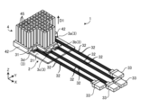
- FIG. 1 is a perspective view of a semiconductor module according to an embodiment, seen obliquely from above.
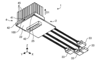
- FIG. 2 is a perspective view of the semiconductor module according to the embodiment, as viewed obliquely from below.
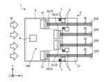
- FIG. 3 is a plan view of the semiconductor module according to the embodiment.
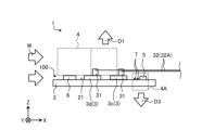
- FIG. 4 is a side view of the semiconductor module according to the embodiment.
- FIG. 5 is a plan view of a semiconductor module according to another embodiment 1.
- FIG. FIG. 6 is a plan view of a semiconductor module according to another embodiment 2.
- FIG. FIG. 7 is a plan view of a semiconductor module according to another embodiment 3.
- FIG. FIG. 8 is a side view of a semiconductor module according to another embodiment 3.
- FIG. 9 is a cross-sectional view taken along line AA of FIG.
- FIG. 10 is a perspective view of a semiconductor module according to another embodiment 4, as viewed obliquely from above.
- FIG. 11 is a cross-sectional view taken along line BB of FIG.
- drawings referenced below may show an orthogonal coordinate system that defines the X-axis, Y-axis, and Z-axis directions that are mutually perpendicular, with the positive Z-axis direction being the vertically upward direction.
- semiconductor modules have been known in which semiconductor elements (hereinafter also referred to as optical elements) that convert electrical signals into optical signals are mounted on a substrate.
- these semiconductor modules are connected to optical fiber cables that transmit the converted optical signals from the optical elements to the outside.
- Fig. 1 is a perspective view of the semiconductor module 1 according to the embodiment as viewed obliquely from above
- Fig. 2 is a perspective view of the semiconductor module 1 according to the embodiment as viewed obliquely from below.
- the semiconductor module 1 is described as an optical module in which an optical element 3 is mounted on a substrate, but the semiconductor module according to the present disclosure does not necessarily have to be an optical module.
- the semiconductor module 1 includes a substrate 2, a plurality of optical elements 3 (optical elements 3a to 3d), and a heat dissipation member 4.
- the optical elements 3 are an example of semiconductor elements.
- the substrate 2 has, for example, a rectangular plate shape when viewed from above.
- a power supply IC 5, a control IC 6, a chip resistor 7 (all see FIG. 3), etc. are located on a first surface 21 (here, the top surface) of the substrate 2.
- a capacitor and a coil may also be located on the first surface 21 of the substrate 2.
- a connector 25 is located on the second surface 22 (here, the bottom surface) of the substrate 2.
- the substrate 2 is electrically connected to the motherboard via the connector 25.
- the optical element 3 is a semiconductor element that converts an electrical signal into an optical signal.
- the optical element 3 may also convert an optical signal into an electrical signal.
- An interface unit 31 is located on the upper surface of each optical element 3.
- the interface unit 31 is connected to an optical connector 33 via a cable group 32A (see FIG. 3) that is made up of multiple optical fiber cables 32.
- cable group 32A see FIG. 3
- the heat dissipation member 4 is a so-called heat sink, and is located above the multiple optical elements 3. Note that the heat dissipation member 4 does not necessarily have to cover the entire upper surface of the multiple optical elements 3. In other words, as shown in FIG. 1, the upper surfaces of the multiple optical elements 3 may be partially exposed from the heat dissipation member 4.
- the heat dissipation member 4 is in close proximity to the multiple optical elements 3 and dissipates heat generated from the optical elements 3 to the outside of the semiconductor module 1.
- the heat dissipation member 4 may be in direct contact with the optical elements 3.
- the heat dissipation member 4 may be in contact with the optical elements 3 via a TIM (Thermal Interface Material).
- the heat dissipation member 4 may be thermally connected to the multiple optical elements 3.
- the heat dissipation member 4 may be made of a metal with a relatively high thermal conductivity, such as aluminum, copper, or iron.
- TIM is a composite material that contains a thermally conductive filler in a resin.
- the heat dissipation member 4 has a first portion 41, multiple third portions 42, and multiple second portions 45.
- the first portion 41 is a plate-shaped portion that faces the first surface 21 of the substrate 2 with a first gap G1 (see FIG. 11) between them.
- the third portions 42 are leg-shaped portions provided on the first portion 41. Specifically, the third portions 42 extend from the first portion 41 toward the substrate 2 and contact the substrate 2 (are placed on the substrate 2). The third portions 42 are also positioned at a third distance G3 (see FIG. 11) from each other along the fourth direction D4 (see FIG. 11).
- third portions 42 are shaped so that their thickness increases partially from the first portion 41.
- the third portions 42 may be integrated with the first portion 41.
- the multiple third portions 42 may be connected to the first portion 41 and the substrate 2.
- the multiple third portions 42 extend in a fixed direction (here, the X-axis direction).
- the second portion 45 is located on the surface of the first portion 41 opposite the surface facing the substrate 2, and extends from the first portion 41 along the first direction D1.
- Figs. 1 and 2 show an example in which the second portion 45 has a pin shape (i.e., a heat dissipation pin), the second portion 45 may also have a plate shape (i.e., a heat dissipation fin), for example.
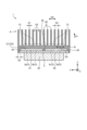
- Fig. 3 is a plan view of the semiconductor module 1 according to the embodiment
- Fig. 4 is a side view of the semiconductor module 1 according to the embodiment. Note that in Figs. 3 and 4, the heat dissipation member 4 is indicated by dashed lines for ease of understanding.
- the first direction D1 in which the heat dissipation member 4 extends relative to the optical element 3 is the positive direction of the Z axis.
- the first direction D1 in which the heat dissipation member 4 dissipates heat is the positive direction of the Z axis.
- the second direction D2 in which the optical fiber cable 32 extends from the optical element 3 is the positive direction of the X axis.
- the first direction D1 in which the heat dissipation member 4 extends relative to the optical element 3 and the second direction D2 in which the optical fiber cable 32 extends may intersect. This allows the heat generated in the optical element 3 to be dissipated in a direction away from the optical fiber cable 32, making it possible to uniform the temperature distribution in the extension direction of the optical fiber cable 32.
- the embodiment it is possible to prevent deterioration of signal quality due to uneven temperature distribution in the optical fiber cable 32, thereby improving the signal quality of the optical signal.
- the cable group 32A is preferably arranged so as to have a portion parallel to the first surface 21 above the substrate 2.
- the portion of the cable group 32A parallel to the substrate 2 is preferably located on the optical element 3 side to which the cable group 32A is connected.
- the cable group 32A may be gradually curved in a direction from the optical element 3 side to which the cable group 32A is connected to the end side of the substrate 2 in the direction in which the cable group 32A extends.
- the cable group 32A may be partially curved near the end of the substrate 2 so as to approach the first surface 21 of the substrate 2 or to contact the first surface 21 of the substrate 2.
- the cable group 32A may be oriented away from the first surface 21 of the substrate 2 near the end of the substrate 2. This is because the orientation of the cable group 32A changes depending on the arrangement and height of the external circuit device to which the cable group 32A is connected.
- the optical fiber cable 32 (or the cable group 32A) may be parallel to the first surface 21 at least above the substrate 2. This can further uniform the temperature distribution in the extension direction of the optical fiber cable 32 (or the cable group 32A).
- the optical fiber cable 32 (or the cable group 32A) extends parallel to the first surface 21 of the substrate 2 over the entire range from the connection portion with the optical element 3 above the substrate 2 to the end of the substrate 2.
- the airflow (heat) hitting the bent part is likely to become turbulent, which can hinder heat dissipation.
- the signal quality of the optical signal can be further improved.
- the multiple optical elements 3a to 3d are arranged along a direction (Y-axis direction) perpendicular to the extension direction (X-axis direction) of the optical fiber cable 32 when viewed along the extension direction. Specifically, the multiple optical elements 3a to 3d are arranged in the positive Y-axis direction in the order of optical element 3d, optical element 3c, optical element 3b, and optical element 3a.
- the multiple optical elements 3a to 3d are positioned apart from each other. With this configuration, when multiple optical elements 3a to 3d are positioned on the substrate 2, it is possible to reduce thermal interference between the optical elements 3a to 3d.
- optical element 3a and optical element 3b located closest to optical element 3a are offset from each other in the extension direction (X-axis direction) of optical fiber cable 32 and in a direction perpendicular to said extension direction (Y-axis direction).
- optical element 3d and optical element 3c located closest to optical element 3d are offset from each other in the X-axis direction and Y-axis direction.
- the multiple optical elements 3 are arranged with a mutual offset. This allows the size of the substrate 2 to be reduced while ensuring the distance between adjacent optical elements 3, in other words, suppressing thermal interference between adjacent optical elements 3, in this embodiment.
- the present disclosure is not limited to this, and in all of the multiple optical elements 3a to 3d, the positions of two adjacent semiconductor elements may be shifted in the extension direction of the optical fiber cable 32 (X-axis direction) and in a direction perpendicular to the extension direction (Y-axis direction).
- the optical elements 3a to 3d may be arranged in a staggered manner. This also makes it possible to reduce the size of the substrate 2 while suppressing thermal interference between the optical elements 3.
- a blower (not shown), such as a cooling fan, that blows air toward the semiconductor module 1 may be located on the negative X-axis side of the semiconductor module 1. Such a blower generates wind W that blows in the positive X-axis direction.
- the wind W sent from the blower hits the multiple second parts 45 (see FIG. 1) and flows along the first surface 21 of the substrate 2, passing through the ventilation passage 100 formed between the substrate 2 and the first part 41 of the heat dissipation member 4.
- the wind W hits the multiple light elements 3 located on the outlet side of the ventilation passage 100, thereby further increasing the heat dissipation efficiency of the multiple light elements 3.
- the multiple light elements 3 are arranged in a direction (here, the Y-axis direction) that intersects with the flow direction of the wind W, so that the wind W hits all the light elements 3 approximately evenly. Therefore, according to the embodiment, the heat dissipation efficiency of the multiple light elements 3 can be further improved.
- control IC 6 may be located below the heat dissipation member 4.
- the control IC 6 may be thermally connected to the heat dissipation member 4. This allows the heat generated by the control IC 6 to be efficiently dissipated by the heat dissipation member 4.
- multiple power supply ICs 5 may be located on the substrate 2. This allows power to be supplied to the optical element 3 at multiple reference voltages (four in FIG. 3).
- the power supply IC 5 may be located on the opposite side of the control IC 6 with respect to the optical element 3.
- the control IC 6 may be located on the negative X-axis side of the optical element 3
- the power supply IC 5 may be located on the positive X-axis side of the optical element 3.
- the multiple chip resistors 7 may be located close to the corresponding power supply ICs 5. In other words, the multiple chip resistors 7 may be located on the opposite side of the control IC 6 with respect to the optical element 3 when the first surface 21 is viewed in plan.
- At least one of the power supply IC 5 and the chip resistor 7 may be located adjacent to the optical fiber cable 32 but not overlapping with the optical fiber cable 32 when the first surface 21 is viewed in a plan view.
- At least one of the power supply IC 5 and the chip resistor 7 should be located in a position that does not overlap with the optical element 3 in the X-axis direction when the first surface 21 is viewed in a plan view.
- both the power supply IC 5 and the chip resistor 7 are positioned so as not to overlap the optical element 3 when viewed in the X-axis direction when the first surface 21 is viewed in a plan view.
- At least one of the power supply IC 5 and the chip resistor 7 may be located between adjacent cable groups 32A when the first surface 21 is viewed in plan.
- the temperature distribution in the extension direction of the optical fiber cable 32 can be made uniform.
- the signal quality of the optical signal can be improved.
- either the power supply IC 5 or the chip resistor 7 may be located in a position that does not overlap with the optical fiber cable 32, or both the power supply IC 5 and the chip resistor 7 may be located in a position that does not overlap with the optical fiber cable 32.
- the signal quality of the optical signal can be further improved.
- Fig. 5 is a plan view of the semiconductor module 1 according to another embodiment 1.
- the arrangement of the power supply ICs 5 and chip resistors 7 differs from that of the above-described embodiment. Specifically, in another embodiment 1, all of the light elements 3 and all of the power supply ICs 5 may be positioned in locations where they do not interfere with each other with respect to the wind W blown from the outside along the first surface 21 of the substrate 2.
- the chip resistor 7 may be positioned upwind of the corresponding power supply IC 5 with respect to the wind W blown from the outside along the first surface 21 of the substrate 2.
- all power supply ICs 5 and all chip resistors 7 are efficiently cooled by the wind W, which reduces the local increase in temperature of the optical fiber cable 32 caused by heat generated by the power supply ICs 5 and chip resistors 7.
- the temperature distribution in the extension direction of the optical fiber cable 32 can be made uniform. Therefore, according to alternative embodiment 1, the signal quality of the optical signal can be improved.
- the width of the power supply IC 5 is wider than the width of the chip resistor 7.
- the width refers to the length in the direction parallel to the first surface 21 of the substrate 2. In FIG. 5, it is the length in the Y-axis direction.
- the wider power supply IC 5 may be arranged behind the chip resistor 7.
- the wide power supply IC 5 has a portion that extends beyond the width of the chip resistor 7, so even if the power supply IC 5 is placed downstream of the chip resistor 7 in the direction of the wind W flow, it is likely that the wind W will hit the power supply IC 5, even if only partially.
- the power supply IC 5 may be larger in either height (thickness) or width than the chip resistor 7, but it may also be larger in both height (thickness) and width.
- Fig. 6 is a plan view of a semiconductor module 1 according to another embodiment 2.
- the configuration of the heat dissipation member 4 is different from that of the above-mentioned embodiment.
- the heat dissipation member 4 may be located not only above the optical element 3 and the control IC 6, but also above the power supply IC 5 and the chip resistor 7.
- At least one of the power supply IC 5 and the chip resistor 7 may be thermally connected to the heat dissipation member 4. This allows the heat generated from at least one of the power supply IC 5 and the chip resistor 7 to be efficiently dissipated by the heat dissipation member 4.
- At least one of the power supply IC 5 and the chip resistor 7 is thermally connected to the heat dissipation member 4, thereby reducing the local increase in temperature of the optical fiber cable 32 caused by heat generated from at least one of the power supply IC 5 and the chip resistor 7.
- the temperature distribution in the extension direction of the optical fiber cable 32 can be made uniform. Therefore, according to alternative embodiment 2, the signal quality of the optical signal can be improved.
- either the power supply IC 5 or the chip resistor 7 may be thermally connected to the heat dissipation member 4, or both the power supply IC 5 and the chip resistor 7 may be thermally connected to the heat dissipation member 4.
- Fig. 7 is a plan view of the semiconductor module 1 according to another embodiment 3
- Fig. 8 is a side view of the semiconductor module 1 according to another embodiment 3.
- Fig. 9 is a cross-sectional view taken along line AA in Fig. 7.
- another heat dissipation member 4A may be provided on the semiconductor module 1.
- the other heat dissipation member 4A may be formed of a metal with a relatively high thermal conductivity, such as aluminum, copper, or iron.
- the separate heat dissipation member 4A may be disposed on top of the power supply IC 5 and the chip resistor 7, as shown in FIG. 7.
- the separate heat dissipation member 4A may also be positioned so as to extend from above the first surface 21 of the substrate 2, around the side surface 23 of the substrate 2, and around the periphery of the second surface 22, as shown in FIG. 9.
- At least one of the power supply IC 5 and the chip resistor 7 may be thermally connected to another heat dissipation member 4A. This allows the heat generated from at least one of the power supply IC 5 and the chip resistor 7 to be efficiently dissipated by the other heat dissipation member 4A.
- the temperature distribution in the extension direction of the optical fiber cable 32 can be made uniform. Therefore, according to alternative embodiment 3, the signal quality of the optical signal can be improved.
- the third direction D3 in which the separate heat dissipation member 4A dissipates heat may be oriented in a direction different from the first direction D1 in which the heat dissipation member 4 dissipates heat.
- the first direction D1 in which the heat dissipation member 4 dissipates heat may be the positive direction of the Z axis
- the third direction D3 in which the separate heat dissipation member 4A dissipates heat may be the negative direction of the Z axis.
- optical element 3 power supply IC 5, control IC 6 and chip resistor 7 located on the first surface 21 of the substrate 2 to be cooled even more efficiently.
- the third direction D3 in which the other heat dissipation member 4A dissipates heat is directed toward the second surface 22 of the substrate 2, thereby reducing the local increase in temperature of the optical fiber cable 32 caused by heat generated from at least one of the power supply IC 5 and the chip resistor 7.
- the temperature distribution in the extension direction of the optical fiber cable 32 can be made uniform. Therefore, according to alternative embodiment 3, the signal quality of the optical signal can be improved.
- the separate heat dissipation member 4A and the optical fiber cable 32 may be spaced apart from each other. This reduces the transfer of heat from the separate heat dissipation member 4A to the optical fiber cable 32, making it possible to homogenize the temperature distribution in the extension direction of the optical fiber cable 32.
- the signal quality of the optical signal can be improved.
- a heat insulating member may be positioned between the other heat dissipation member 4A and the optical fiber cable 32. This also makes it possible to reduce the transfer of heat from the other heat dissipation member 4A to the optical fiber cable 32.
- the separate heat dissipation member 4A may have a substantially C-shape in cross section. This allows the separate heat dissipation member 4A to be fixed to the substrate 2 by fitting the separate heat dissipation member 4A from above the substrate 2.
- another heat dissipation member 4A can be easily attached to the substrate 2.
- FIG. 10 is a perspective view of a semiconductor module 1 according to another embodiment 4, as viewed obliquely from above, and FIG. 11 is a cross-sectional view taken along line BB in FIG.
- the configuration of the second portion 45 of the heat dissipation member 4 differs from that of the above-described embodiment (see Figure 1).
- the second portion 45 may be a plate-shaped heat dissipation fin extending from the first portion 41 along the first direction D1.
- multiple second portions 45 are positioned at a second interval G2 from each other along a fourth direction D4 (e.g., the Y-axis direction) that intersects with the second direction D2 (see FIG. 10).
- a fourth direction D4 e.g., the Y-axis direction
- the dimension S1 of the second portion 45 in the fourth direction D4 can be made smaller than when the second portion 45 is a heat dissipation pin, making it possible to reduce the weight of the heat dissipation member 4.
- the second gap G2 (see FIG. 11) between adjacent second portions 45 may extend along the second direction D2. This allows the wind W (see FIG. 3) sent from a blower (not shown) to flow smoothly along the second gap G2, so that the wind W hits all of the second portions 45 approximately evenly.
- the heat dissipation efficiency of the heat dissipation member 4 can be further improved.
- the dimension S1 of the second portion 45 in the fourth direction D4 may be smaller than the dimension S2 of the third portion 42 in the fourth direction D4. In this way, by reducing the dimension S1 of the second portion 45 (i.e., making the second portion 45 thinner), the desired heat dissipation efficiency can be achieved even if the heat dissipation member 4 is made smaller and thinner.
- the dimension S1 of the second portion 45 in the fourth direction D4 may be, for example, 0.5 mm to 1.0 mm, and more specifically, is approximately 0.6 mm.
- the dimension S2 of the third portion 42 may be, for example, 1 mm or more.
- the dimension S4 of the interface portion 31 in the fourth direction D4 may satisfy the following formula (1). S4 ⁇ 2 ⁇ S1+2 ⁇ S3 (1)
- the dimensions of the heat dissipation member 4 should be specified so that not only the thickness of the second portion 45 (i.e., dimension S1) but also the pitch between the multiple second portions 45 (i.e., dimension S3) is small, based on the dimension S4 in the fourth direction D4 of the interface portion 31.
- the present technology can also be configured as follows. (1) A substrate; at least one semiconductor device located on a first surface of the substrate; a heat dissipation member located above the semiconductor element; an optical fiber cable connected to the semiconductor device; Equipped with a first direction in which the heat dissipation member extends relative to the semiconductor element and a second direction in which the optical fiber cable extends intersect with each other. (2) The semiconductor module according to (1), wherein the optical fiber cable has at least a portion parallel to the first surface above the substrate.
- At least one power supply IC located on the first surface and supplying power to the semiconductor device; at least one chip resistor located on the first surface and electrically connected to the power supply IC; Further equipped with The semiconductor module described in (1) or (2), wherein at least one of the power supply IC and the chip resistor is located adjacent to the optical fiber cable and does not overlap with the optical fiber cable when viewed in a planar view of the first surface.
- the semiconductor module according to (3) wherein the semiconductor element and the power supply IC are positioned so as not to interfere with each other with respect to wind blown from the outside along the first surface of the substrate.
- the heat dissipation member has at least a plate-like first portion positioned opposite the substrate with a first distance therebetween, and a plurality of second portions extending from the first portion along the first direction,
- the semiconductor module according to any one of (1) to (8), wherein the second portion is a plate-shaped heat dissipation fin extending along the first direction.
- the second portions are positioned at second intervals from each other along a fourth direction intersecting the second direction, The semiconductor module according to (9), wherein the second interval extends along the second direction.
- the heat dissipation member further includes a plurality of third portions extending from the first portion toward the substrate and in contact with the substrate, the third portions being spaced apart from each other along the fourth direction,
- the semiconductor module according to (10) wherein a dimension of the second portion in the fourth direction is smaller than a dimension of the third portion in the fourth direction.
Landscapes
- Optical Couplings Of Light Guides (AREA)
Priority Applications (3)
| Application Number | Priority Date | Filing Date | Title |
|---|---|---|---|
| CN202380066637.8A CN119895565A (zh) | 2022-09-26 | 2023-09-26 | 半导体模块 |
| EP23872333.2A EP4597565A1 (en) | 2022-09-26 | 2023-09-26 | Semiconductor module |
| JP2024549418A JPWO2024071110A1 (https=) | 2022-09-26 | 2023-09-26 |
Applications Claiming Priority (2)
| Application Number | Priority Date | Filing Date | Title |
|---|---|---|---|
| JP2022152741 | 2022-09-26 | ||
| JP2022-152741 | 2022-09-26 |
Publications (1)
| Publication Number | Publication Date |
|---|---|
| WO2024071110A1 true WO2024071110A1 (ja) | 2024-04-04 |
Family
ID=90478003
Family Applications (1)
| Application Number | Title | Priority Date | Filing Date |
|---|---|---|---|
| PCT/JP2023/034917 Ceased WO2024071110A1 (ja) | 2022-09-26 | 2023-09-26 | 半導体モジュール |
Country Status (4)
| Country | Link |
|---|---|
| EP (1) | EP4597565A1 (https=) |
| JP (1) | JPWO2024071110A1 (https=) |
| CN (1) | CN119895565A (https=) |
| WO (1) | WO2024071110A1 (https=) |
Citations (7)
| Publication number | Priority date | Publication date | Assignee | Title |
|---|---|---|---|---|
| JP2001007403A (ja) * | 1999-06-23 | 2001-01-12 | Nec Corp | 並列伝送型光モジュールおよびその製造方法 |
| JP2005064384A (ja) * | 2003-08-19 | 2005-03-10 | Toshiba Corp | インターフェイスモジュール付lsiパッケージ及びそれに用いるヒートシンク |
| JP2010211157A (ja) * | 2009-03-12 | 2010-09-24 | Hitachi Cable Ltd | 光送受信器 |
| JP2014178383A (ja) * | 2013-03-13 | 2014-09-25 | Hitachi Metals Ltd | 通信モジュール及びそれを備えた信号伝送装置 |
| JP2015084040A (ja) * | 2013-10-25 | 2015-04-30 | 日立金属株式会社 | 光通信モジュール |
| JP2016031990A (ja) * | 2014-07-28 | 2016-03-07 | 日立金属株式会社 | 光電気変換モジュールおよび光電気変換モジュールを用いた伝送装置 |
| JP2020009824A (ja) | 2018-07-04 | 2020-01-16 | 沖電気工業株式会社 | 光通信装置、及び光通信装置の製造方法 |
-
2023
- 2023-09-26 WO PCT/JP2023/034917 patent/WO2024071110A1/ja not_active Ceased
- 2023-09-26 EP EP23872333.2A patent/EP4597565A1/en not_active Withdrawn
- 2023-09-26 CN CN202380066637.8A patent/CN119895565A/zh active Pending
- 2023-09-26 JP JP2024549418A patent/JPWO2024071110A1/ja active Pending
Patent Citations (7)
| Publication number | Priority date | Publication date | Assignee | Title |
|---|---|---|---|---|
| JP2001007403A (ja) * | 1999-06-23 | 2001-01-12 | Nec Corp | 並列伝送型光モジュールおよびその製造方法 |
| JP2005064384A (ja) * | 2003-08-19 | 2005-03-10 | Toshiba Corp | インターフェイスモジュール付lsiパッケージ及びそれに用いるヒートシンク |
| JP2010211157A (ja) * | 2009-03-12 | 2010-09-24 | Hitachi Cable Ltd | 光送受信器 |
| JP2014178383A (ja) * | 2013-03-13 | 2014-09-25 | Hitachi Metals Ltd | 通信モジュール及びそれを備えた信号伝送装置 |
| JP2015084040A (ja) * | 2013-10-25 | 2015-04-30 | 日立金属株式会社 | 光通信モジュール |
| JP2016031990A (ja) * | 2014-07-28 | 2016-03-07 | 日立金属株式会社 | 光電気変換モジュールおよび光電気変換モジュールを用いた伝送装置 |
| JP2020009824A (ja) | 2018-07-04 | 2020-01-16 | 沖電気工業株式会社 | 光通信装置、及び光通信装置の製造方法 |
Also Published As
| Publication number | Publication date |
|---|---|
| EP4597565A1 (en) | 2025-08-06 |
| JPWO2024071110A1 (https=) | 2024-04-04 |
| CN119895565A (zh) | 2025-04-25 |
Similar Documents
| Publication | Publication Date | Title |
|---|---|---|
| US20250247945A1 (en) | Working assembly and electronic device | |
| US7898806B2 (en) | Motor controller | |
| JP7339075B2 (ja) | 電気機器、電子制御装置 | |
| CN201115256Y (zh) | 散热装置 | |
| US7957143B2 (en) | Motor controller | |
| JPH07283564A (ja) | 電子装置 | |
| JP2010187504A (ja) | インバータ装置 | |
| CN113597823A (zh) | 电子控制装置 | |
| JP6222938B2 (ja) | 放熱装置 | |
| US12114467B2 (en) | Heatsink with increased air flow | |
| WO2023100480A1 (ja) | 電子制御装置 | |
| WO2024071110A1 (ja) | 半導体モジュール | |
| CN116266982B (zh) | 电源装置 | |
| US20250164719A1 (en) | Semiconductor module | |
| US20260099020A1 (en) | Semiconductor module | |
| JPH10256766A (ja) | 電子機器の強制空冷構造 | |
| US20080068794A1 (en) | Dissipation module and electronic device having the same | |
| TWI859951B (zh) | 散熱系統及環形散熱器 | |
| CN217825796U (zh) | 双面散热器和用电设备 | |
| CN111031754A (zh) | Pcb散热组件和具有其的服务器 | |
| WO2025052864A1 (ja) | 放熱部材、及びそれを備える電気機器並びにモータ装置 | |
| TW202529513A (zh) | 散熱模組及電子裝置 | |
| WO2024071244A1 (ja) | 半導体モジュール | |
| HK40091906A (zh) | 电子设备 | |
| JP2006179610A (ja) | 放熱板固定構造 |
Legal Events
| Date | Code | Title | Description |
|---|---|---|---|
| 121 | Ep: the epo has been informed by wipo that ep was designated in this application |
Ref document number: 23872333 Country of ref document: EP Kind code of ref document: A1 |
|
| WWE | Wipo information: entry into national phase |
Ref document number: 202380066637.8 Country of ref document: CN |
|
| WWE | Wipo information: entry into national phase |
Ref document number: 2024549418 Country of ref document: JP |
|
| WWP | Wipo information: published in national office |
Ref document number: 202380066637.8 Country of ref document: CN |
|
| WWE | Wipo information: entry into national phase |
Ref document number: 2023872333 Country of ref document: EP |
|
| NENP | Non-entry into the national phase |
Ref country code: DE |
|
| ENP | Entry into the national phase |
Ref document number: 2023872333 Country of ref document: EP Effective date: 20250428 |
|
| WWP | Wipo information: published in national office |
Ref document number: 2023872333 Country of ref document: EP |
|
| WWW | Wipo information: withdrawn in national office |
Ref document number: 2023872333 Country of ref document: EP |