WO2024071110A1 - Semiconductor module - Google Patents
Semiconductor module Download PDFInfo
- Publication number
- WO2024071110A1 WO2024071110A1 PCT/JP2023/034917 JP2023034917W WO2024071110A1 WO 2024071110 A1 WO2024071110 A1 WO 2024071110A1 JP 2023034917 W JP2023034917 W JP 2023034917W WO 2024071110 A1 WO2024071110 A1 WO 2024071110A1
- Authority
- WO
- WIPO (PCT)
- Prior art keywords
- heat dissipation
- substrate
- dissipation member
- semiconductor module
- power supply
- Prior art date
Links
- 239000004065 semiconductor Substances 0.000 title claims abstract description 83
- 230000017525 heat dissipation Effects 0.000 claims abstract description 92
- 239000000758 substrate Substances 0.000 claims abstract description 68
- 239000013307 optical fiber Substances 0.000 claims description 53
- 239000000835 fiber Substances 0.000 abstract 2
- 230000003287 optical effect Effects 0.000 description 94
- XEEYBQQBJWHFJM-UHFFFAOYSA-N Iron Chemical compound [Fe] XEEYBQQBJWHFJM-UHFFFAOYSA-N 0.000 description 4
- 230000014509 gene expression Effects 0.000 description 3
- RYGMFSIKBFXOCR-UHFFFAOYSA-N Copper Chemical compound [Cu] RYGMFSIKBFXOCR-UHFFFAOYSA-N 0.000 description 2
- 229910052782 aluminium Inorganic materials 0.000 description 2
- XAGFODPZIPBFFR-UHFFFAOYSA-N aluminium Chemical compound [Al] XAGFODPZIPBFFR-UHFFFAOYSA-N 0.000 description 2
- 229910052802 copper Inorganic materials 0.000 description 2
- 239000010949 copper Substances 0.000 description 2
- 230000006866 deterioration Effects 0.000 description 2
- 229910052742 iron Inorganic materials 0.000 description 2
- 229910052751 metal Inorganic materials 0.000 description 2
- 239000002184 metal Substances 0.000 description 2
- 238000012986 modification Methods 0.000 description 2
- 230000004048 modification Effects 0.000 description 2
- 238000012546 transfer Methods 0.000 description 2
- 238000009423 ventilation Methods 0.000 description 2
- 238000013459 approach Methods 0.000 description 1
- 239000003990 capacitor Substances 0.000 description 1
- 239000002131 composite material Substances 0.000 description 1
- 239000011231 conductive filler Substances 0.000 description 1
- 230000008094 contradictory effect Effects 0.000 description 1
- 238000001816 cooling Methods 0.000 description 1
- 238000013461 design Methods 0.000 description 1
- 238000009434 installation Methods 0.000 description 1
- 238000004519 manufacturing process Methods 0.000 description 1
- 239000000463 material Substances 0.000 description 1
- 238000012545 processing Methods 0.000 description 1
- 239000011347 resin Substances 0.000 description 1
- 229920005989 resin Polymers 0.000 description 1
Images


Classifications
-
- H—ELECTRICITY
- H01—ELECTRIC ELEMENTS
- H01L—SEMICONDUCTOR DEVICES NOT COVERED BY CLASS H10
- H01L23/00—Details of semiconductor or other solid state devices
- H01L23/34—Arrangements for cooling, heating, ventilating or temperature compensation ; Temperature sensing arrangements
- H01L23/40—Mountings or securing means for detachable cooling or heating arrangements ; fixed by friction, plugs or springs
-
- H—ELECTRICITY
- H01—ELECTRIC ELEMENTS
- H01L—SEMICONDUCTOR DEVICES NOT COVERED BY CLASS H10
- H01L25/00—Assemblies consisting of a plurality of individual semiconductor or other solid state devices ; Multistep manufacturing processes thereof
- H01L25/03—Assemblies consisting of a plurality of individual semiconductor or other solid state devices ; Multistep manufacturing processes thereof all the devices being of a type provided for in the same subgroup of groups H01L27/00 - H01L33/00, or in a single subclass of H10K, H10N, e.g. assemblies of rectifier diodes
- H01L25/04—Assemblies consisting of a plurality of individual semiconductor or other solid state devices ; Multistep manufacturing processes thereof all the devices being of a type provided for in the same subgroup of groups H01L27/00 - H01L33/00, or in a single subclass of H10K, H10N, e.g. assemblies of rectifier diodes the devices not having separate containers
-
- H—ELECTRICITY
- H01—ELECTRIC ELEMENTS
- H01L—SEMICONDUCTOR DEVICES NOT COVERED BY CLASS H10
- H01L25/00—Assemblies consisting of a plurality of individual semiconductor or other solid state devices ; Multistep manufacturing processes thereof
- H01L25/18—Assemblies consisting of a plurality of individual semiconductor or other solid state devices ; Multistep manufacturing processes thereof the devices being of types provided for in two or more different subgroups of the same main group of groups H01L27/00 - H01L33/00, or in a single subclass of H10K, H10N
-
- H—ELECTRICITY
- H05—ELECTRIC TECHNIQUES NOT OTHERWISE PROVIDED FOR
- H05K—PRINTED CIRCUITS; CASINGS OR CONSTRUCTIONAL DETAILS OF ELECTRIC APPARATUS; MANUFACTURE OF ASSEMBLAGES OF ELECTRICAL COMPONENTS
- H05K7/00—Constructional details common to different types of electric apparatus
- H05K7/20—Modifications to facilitate cooling, ventilating, or heating
Landscapes
- Engineering & Computer Science (AREA)
- Microelectronics & Electronic Packaging (AREA)
- Physics & Mathematics (AREA)
- Power Engineering (AREA)
- Condensed Matter Physics & Semiconductors (AREA)
- General Physics & Mathematics (AREA)
- Computer Hardware Design (AREA)
- Thermal Sciences (AREA)
- Optical Couplings Of Light Guides (AREA)
Abstract
This semiconductor module comprises a substrate, at least one semiconductor element that is positioned on a first surface of the substrate, a heat dissipation member that is positioned above the semiconductor element, and an optic fiber cable that is connected to the semiconductor element. A first direction in which the heat dissipation member extends relative to the semiconductor element and a second direction in which the optic fiber cable extends intersect each other.
Description
開示の実施形態は、半導体モジュールに関する。
The disclosed embodiment relates to a semiconductor module.
従来より、電気信号を光信号に変換する半導体素子(以下、光素子とも呼称する。)が基板上に実装された半導体モジュールが知られている。この半導体モジュールには、変換された光信号を光素子から外部に伝達する光ファイバーケーブルが接続される場合がある(特許文献1参照)。
Conventionally, semiconductor modules have been known in which semiconductor elements (hereinafter also referred to as optical elements) that convert electrical signals into optical signals are mounted on a substrate. In some cases, these semiconductor modules are connected to optical fiber cables that transmit the converted optical signals from the optical elements to the outside (see Patent Document 1).
本開示の半導体モジュールは、基板と、前記基板の第1面に位置する少なくとも1つの半導体素子と、前記半導体素子の上方に位置する放熱部材と、前記半導体素子に接続される光ファイバーケーブルと、を備える。また、前記半導体素子に対して前記放熱部材が延びる第1方向と、前記光ファイバーケーブルが延びる第2方向とが交差する。
The semiconductor module disclosed herein comprises a substrate, at least one semiconductor element located on a first surface of the substrate, a heat dissipation member located above the semiconductor element, and an optical fiber cable connected to the semiconductor element. In addition, a first direction in which the heat dissipation member extends relative to the semiconductor element intersects with a second direction in which the optical fiber cable extends.
以下、添付図面を参照して、本願の開示する半導体モジュールの実施形態について説明する。なお、以下に示す実施形態により本開示が限定されるものではない。また、各実施形態は、処理内容を矛盾させない範囲で適宜組み合わせることが可能である。また、以下の各実施形態において同一の部位には同一の符号を付し、重複する説明は省略される。
Below, an embodiment of the semiconductor module disclosed in the present application will be described with reference to the attached drawings. Note that the present disclosure is not limited to the embodiments described below. Furthermore, each embodiment can be appropriately combined as long as the processing content is not contradictory. Furthermore, the same parts in each of the following embodiments are given the same reference numerals, and duplicate explanations will be omitted.
また、以下に示す実施形態では、「一定」、「直交」、「垂直」あるいは「平行」といった表現が用いられる場合があるが、これらの表現は、厳密に「一定」、「直交」、「垂直」あるいは「平行」であることを要しない。すなわち、上記した各表現は、例えば製造精度、設置精度などのずれを許容するものとする。
In addition, in the embodiments described below, expressions such as "constant," "orthogonal," "vertical," and "parallel" may be used, but these expressions do not necessarily mean "constant," "orthogonal," "vertical," or "parallel" in the strict sense. In other words, each of the above expressions allows for deviations due to, for example, manufacturing precision, installation precision, and the like.
また、以下参照する各図面では、説明を分かりやすくするために、互いに直交するX軸方向、Y軸方向およびZ軸方向を規定し、Z軸正方向を鉛直上向き方向とする直交座標系を示す場合がある。
In addition, in order to make the explanation easier to understand, the drawings referenced below may show an orthogonal coordinate system that defines the X-axis, Y-axis, and Z-axis directions that are mutually perpendicular, with the positive Z-axis direction being the vertically upward direction.
従来より、電気信号を光信号に変換する半導体素子(以下、光素子とも呼称する。)が基板上に実装された半導体モジュールが知られている。この半導体モジュールには、変換された光信号を光素子から外部に伝達する光ファイバーケーブルが接続される場合がある。
Conventionally, semiconductor modules have been known in which semiconductor elements (hereinafter also referred to as optical elements) that convert electrical signals into optical signals are mounted on a substrate. In some cases, these semiconductor modules are connected to optical fiber cables that transmit the converted optical signals from the optical elements to the outside.
しかしながら、上述の従来技術では、半導体モジュールに搭載される光素子などの各種素子で発生する熱に起因して、光ファイバーケーブルの延在方向における熱分布が不均一となる場合があった。これにより、光ファイバーケーブル内を伝達する光信号の信号品質が低下する恐れがあった。
However, in the above-mentioned conventional technology, heat generated by various elements, such as optical elements, mounted on the semiconductor module can cause uneven heat distribution in the extension direction of the optical fiber cable. This can lead to a deterioration in the signal quality of the optical signal transmitted through the optical fiber cable.
そこで、上述の問題点を克服し、光信号の信号品質を向上させることができる技術の実現が期待されている。
Therefore, there is a need to develop technology that can overcome the problems mentioned above and improve the signal quality of optical signals.
<実施形態>
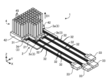
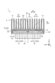
まず、実施形態に係る半導体モジュール1の全体構成について、図1および図2を参照しながら説明する。図1は、実施形態に係る半導体モジュール1を斜め上方から見た斜視図であり、図2は、実施形態に係る半導体モジュール1を斜め下方から見た斜視図である。 <Embodiment>
First, the overall configuration of asemiconductor module 1 according to an embodiment will be described with reference to Fig. 1 and Fig. 2. Fig. 1 is a perspective view of the semiconductor module 1 according to the embodiment as viewed obliquely from above, and Fig. 2 is a perspective view of the semiconductor module 1 according to the embodiment as viewed obliquely from below.
まず、実施形態に係る半導体モジュール1の全体構成について、図1および図2を参照しながら説明する。図1は、実施形態に係る半導体モジュール1を斜め上方から見た斜視図であり、図2は、実施形態に係る半導体モジュール1を斜め下方から見た斜視図である。 <Embodiment>
First, the overall configuration of a
なお、以下に示す各実施形態では、半導体モジュール1が光素子3を基板上に実装した光モジュールである場合を例に挙げて説明するが、本開示による半導体モジュールは、必ずしも光モジュールであることを要しない。
Note that in each of the embodiments described below, the semiconductor module 1 is described as an optical module in which an optical element 3 is mounted on a substrate, but the semiconductor module according to the present disclosure does not necessarily have to be an optical module.
図1および図2に示すように、実施形態に係る半導体モジュール1は、基板2と、複数の光素子3(光素子3a~3d)と、放熱部材4とを備える。光素子3は、半導体素子の一例である。
As shown in Figures 1 and 2, the semiconductor module 1 according to the embodiment includes a substrate 2, a plurality of optical elements 3 (optical elements 3a to 3d), and a heat dissipation member 4. The optical elements 3 are an example of semiconductor elements.
基板2は、たとえば平面視四角形の板形状を有する。基板2の第1面21(ここでは、上面)には、複数の光素子3a~3dおよび放熱部材4の他、電源IC5、制御IC6、チップ抵抗7(いずれも図3参照)などが位置する。また、基板2の第1面21には、図示しないコンデンサおよびコイルなどが位置してもよい。
The substrate 2 has, for example, a rectangular plate shape when viewed from above. In addition to the multiple optical elements 3a-3d and heat dissipation member 4, a power supply IC 5, a control IC 6, a chip resistor 7 (all see FIG. 3), etc. are located on a first surface 21 (here, the top surface) of the substrate 2. In addition, a capacitor and a coil (not shown) may also be located on the first surface 21 of the substrate 2.
基板2の第2面22(ここでは、下面)には、コネクタ25が位置している。基板2は、コネクタ25を介してマザーボードと電気的に接続される。
A connector 25 is located on the second surface 22 (here, the bottom surface) of the substrate 2. The substrate 2 is electrically connected to the motherboard via the connector 25.
光素子3は、電気信号を光信号に変換する半導体素子である。また、光素子3は、光信号を電気信号に変換してもよい。各光素子3の上面には、インタフェース部31が位置する。インタフェース部31は、複数の光ファイバーケーブル32で構成されるケーブル群32A(図3参照)を介して光コネクタ33に接続される。以下、光ファイバーケーブル32と記した場合にも、該当する図に基づいてケーブル群32Aを指す場合がある。
The optical element 3 is a semiconductor element that converts an electrical signal into an optical signal. The optical element 3 may also convert an optical signal into an electrical signal. An interface unit 31 is located on the upper surface of each optical element 3. The interface unit 31 is connected to an optical connector 33 via a cable group 32A (see FIG. 3) that is made up of multiple optical fiber cables 32. Hereinafter, even when optical fiber cable 32 is mentioned, it may refer to cable group 32A based on the relevant figure.
放熱部材4は、いわゆるヒートシンクであり、複数の光素子3の上方に位置する。なお、放熱部材4は、必ずしも複数の光素子3の上方の全てを覆っていなくてもよい。すなわち、図1に示すように、複数の光素子3の上面は、放熱部材4から部分的に露出していてもよい。
The heat dissipation member 4 is a so-called heat sink, and is located above the multiple optical elements 3. Note that the heat dissipation member 4 does not necessarily have to cover the entire upper surface of the multiple optical elements 3. In other words, as shown in FIG. 1, the upper surfaces of the multiple optical elements 3 may be partially exposed from the heat dissipation member 4.
放熱部材4は、複数の光素子3に近接し、光素子3から発生した熱を半導体モジュール1の外部に放出する。なお、放熱部材4は、光素子3と直接接触していてもよい。あるいは、放熱部材4は、光素子3にTIM(Thermal Interface Material)を介して接触していてもよい。すなわち、放熱部材4は、複数の光素子3と熱的に接続されてもよい。
The heat dissipation member 4 is in close proximity to the multiple optical elements 3 and dissipates heat generated from the optical elements 3 to the outside of the semiconductor module 1. The heat dissipation member 4 may be in direct contact with the optical elements 3. Alternatively, the heat dissipation member 4 may be in contact with the optical elements 3 via a TIM (Thermal Interface Material). In other words, the heat dissipation member 4 may be thermally connected to the multiple optical elements 3.
放熱部材4は、たとえばアルミニウム、銅、鉄などの熱伝導率が比較的高い金属で形成されてもよい。TIMとは、樹脂中に熱伝導性のフィラーを含む複合材料のことである。
The heat dissipation member 4 may be made of a metal with a relatively high thermal conductivity, such as aluminum, copper, or iron. TIM is a composite material that contains a thermally conductive filler in a resin.
放熱部材4は、第1部41と、複数の第3部42と、複数の第2部45とを有する。第1部41は、基板2の第1面21と第1間隔G1(図11参照)をあけて対向配置される板状の部位である。
The heat dissipation member 4 has a first portion 41, multiple third portions 42, and multiple second portions 45. The first portion 41 is a plate-shaped portion that faces the first surface 21 of the substrate 2 with a first gap G1 (see FIG. 11) between them.
複数の第3部42は、第1部41に設けられる脚状の部位である。具体的には、第3部42は、第1部41から基板2に向かって延びて基板2に接する(基板2上に据えられる)。また、複数の第3部42は、第4方向D4(図11参照)に沿って互いに第3間隔G3(図11参照)をあけて位置する。
The third portions 42 are leg-shaped portions provided on the first portion 41. Specifically, the third portions 42 extend from the first portion 41 toward the substrate 2 and contact the substrate 2 (are placed on the substrate 2). The third portions 42 are also positioned at a third distance G3 (see FIG. 11) from each other along the fourth direction D4 (see FIG. 11).
これらの第3部42は、第1部41からその厚みが部分的に厚くなる形状を成している。第3部42は第1部41と一体化していてもよい。複数の第3部42は、第1部41と基板2とに接続されていてもよい。複数の第3部42は、一定の方向(ここでは、X軸方向)に延在している。
These third portions 42 are shaped so that their thickness increases partially from the first portion 41. The third portions 42 may be integrated with the first portion 41. The multiple third portions 42 may be connected to the first portion 41 and the substrate 2. The multiple third portions 42 extend in a fixed direction (here, the X-axis direction).
第2部45は、第1部41における基板2との対向面とは反対側の面に位置し、第1部41から第1方向D1に沿って延びる部位である。図1および図2では、第2部45がピン形状を有する場合(すなわち、放熱ピンである場合)の例を示しているが、第2部45は、たとえば板形状(すなわち、放熱フィン)であってもよい。
The second portion 45 is located on the surface of the first portion 41 opposite the surface facing the substrate 2, and extends from the first portion 41 along the first direction D1. Although Figs. 1 and 2 show an example in which the second portion 45 has a pin shape (i.e., a heat dissipation pin), the second portion 45 may also have a plate shape (i.e., a heat dissipation fin), for example.
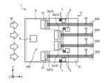
つづいて、実施形態に係る半導体モジュール1の詳細な構成について、図3および図4を参照しながら説明する。図3は、実施形態に係る半導体モジュール1の平面図であり、図4は、実施形態に係る半導体モジュール1の側面図である。なお、図3および図4では、理解を容易にするため、放熱部材4を破線で示している。
Next, the detailed configuration of the semiconductor module 1 according to the embodiment will be described with reference to Figs. 3 and 4. Fig. 3 is a plan view of the semiconductor module 1 according to the embodiment, and Fig. 4 is a side view of the semiconductor module 1 according to the embodiment. Note that in Figs. 3 and 4, the heat dissipation member 4 is indicated by dashed lines for ease of understanding.
図4などに示すように、光素子3に対して放熱部材4が延びる第1方向D1は、Z軸正方向である。すなわち、放熱部材4が放熱する第1方向D1は、Z軸正方向である。一方で、光素子3から光ファイバーケーブル32が延びる第2方向D2は、X軸正方向である。
As shown in FIG. 4 etc., the first direction D1 in which the heat dissipation member 4 extends relative to the optical element 3 is the positive direction of the Z axis. In other words, the first direction D1 in which the heat dissipation member 4 dissipates heat is the positive direction of the Z axis. On the other hand, the second direction D2 in which the optical fiber cable 32 extends from the optical element 3 is the positive direction of the X axis.
すなわち、実施形態では、光素子3に対して放熱部材4が延びる第1方向D1と、光ファイバーケーブル32が延びる第2方向D2とが交差していてもよい。これにより、光素子3で発生する熱を、光ファイバーケーブル32から離れる向きに放熱することができるため、光ファイバーケーブル32の延在方向における温度分布を均一化することができる。
In other words, in the embodiment, the first direction D1 in which the heat dissipation member 4 extends relative to the optical element 3 and the second direction D2 in which the optical fiber cable 32 extends may intersect. This allows the heat generated in the optical element 3 to be dissipated in a direction away from the optical fiber cable 32, making it possible to uniform the temperature distribution in the extension direction of the optical fiber cable 32.
したがって、実施形態によれば、光ファイバーケーブル32における温度分布の不均一化による信号品質の悪化を防ぐことができるため、光信号の信号品質を向上させることができる。
Therefore, according to the embodiment, it is possible to prevent deterioration of signal quality due to uneven temperature distribution in the optical fiber cable 32, thereby improving the signal quality of the optical signal.
また、実施形態では、図4に示すように、ケーブル群32Aは、基板2の上方において第1面21と平行な部分を有するように配置されるのがよい。ケーブル群32Aの基板2に平行な部分は、ケーブル群32Aの中で当該ケーブル群32Aが接続される光素子3側に位置しているのがよい。
In the embodiment, as shown in FIG. 4, the cable group 32A is preferably arranged so as to have a portion parallel to the first surface 21 above the substrate 2. The portion of the cable group 32A parallel to the substrate 2 is preferably located on the optical element 3 side to which the cable group 32A is connected.
ケーブル群32Aは、そのケーブル群32Aが接続される光素子3側からケーブル群32Aが延びている方向の基板2の端部側に至る方向に次第に湾曲していてもよい。例えば、ケーブル群32Aは、基板2の端部付近においては、基板2の第1面21に近づくかまたは基板2の第1面21に接するように一部が曲がっていてもよい。
The cable group 32A may be gradually curved in a direction from the optical element 3 side to which the cable group 32A is connected to the end side of the substrate 2 in the direction in which the cable group 32A extends. For example, the cable group 32A may be partially curved near the end of the substrate 2 so as to approach the first surface 21 of the substrate 2 or to contact the first surface 21 of the substrate 2.
ケーブル群32Aは、基板2の端部付近においては、基板2の第1面21から離れるような向きになってもよい。これは、ケーブル群32Aが接続される外部回路装置の配置や高さとの関係で向きが変化することによる。
The cable group 32A may be oriented away from the first surface 21 of the substrate 2 near the end of the substrate 2. This is because the orientation of the cable group 32A changes depending on the arrangement and height of the external circuit device to which the cable group 32A is connected.
光ファイバーケーブル32(またはケーブル群32A)は、少なくとも基板2の上方において、第1面21と平行であってもよい。これにより、光ファイバーケーブル32(またはケーブル群32A)の延在方向における温度分布をさらに均一化することができる。
The optical fiber cable 32 (or the cable group 32A) may be parallel to the first surface 21 at least above the substrate 2. This can further uniform the temperature distribution in the extension direction of the optical fiber cable 32 (or the cable group 32A).
この場合、光ファイバーケーブル32(またはケーブル群32A)は、基板2の上方における光素子3との接続部分から基板2の端部までの全範囲で基板2の第1面21と平行に延びた状態となっているのがよい。
In this case, it is preferable that the optical fiber cable 32 (or the cable group 32A) extends parallel to the first surface 21 of the substrate 2 over the entire range from the connection portion with the optical element 3 above the substrate 2 to the end of the substrate 2.
基板2の上方で、光ファイバーケーブル32(またはケーブル群32A)の一部が曲がった状態になると、その曲がった部分に当たった気流(熱)が乱流になりやすく、放熱性を妨げやすくなるからである。
If part of the optical fiber cable 32 (or cable group 32A) is bent above the substrate 2, the airflow (heat) hitting the bent part is likely to become turbulent, which can hinder heat dissipation.
したがって、実施形態によれば、光信号の信号品質をさらに向上させることができる。
Therefore, according to the embodiment, the signal quality of the optical signal can be further improved.
図3に示すように、複数の光素子3a~3dは、光ファイバーケーブル32の延在方向(X軸方向)に沿って見た場合に、かかる延在方向と直交する方向(Y軸方向)に沿って並べられる。具体的には、複数の光素子3a~3dは、Y軸正方向に光素子3d、光素子3c、光素子3bおよび光素子3aの順番で並べられる。
As shown in FIG. 3, the multiple optical elements 3a to 3d are arranged along a direction (Y-axis direction) perpendicular to the extension direction (X-axis direction) of the optical fiber cable 32 when viewed along the extension direction. Specifically, the multiple optical elements 3a to 3d are arranged in the positive Y-axis direction in the order of optical element 3d, optical element 3c, optical element 3b, and optical element 3a.
また、複数の光素子3a~3dは、互いに離隔して位置する。かかる構成とすることにより、基板2上に複数の光素子3a~3dが位置する場合に、光素子3a~3d同士の熱干渉を低減することができる。
Furthermore, the multiple optical elements 3a to 3d are positioned apart from each other. With this configuration, when multiple optical elements 3a to 3d are positioned on the substrate 2, it is possible to reduce thermal interference between the optical elements 3a to 3d.
発熱源である光素子3a~3dなどのデバイスを同一基板上に複数個配置する場合に、光素子3a~3d同士の距離が近くなると、個々の光素子3a~3dが発する熱が相乗し、単体での使用時よりも光素子3a~3dの温度が高くなってしまうことがある。
When multiple heat-generating devices such as optical elements 3a-3d are placed on the same board, if the optical elements 3a-3d are placed close to each other, the heat generated by each optical element 3a-3d is multiplied, and the temperature of the optical elements 3a-3d may become higher than when used alone.
複数の光素子3a~3dを図3に示したように隔離して配置にすることにより、個々の光素子3a~3dが発する熱が相乗して高くなることを抑制することが可能になる。電源IC5およびチップ抵抗7を光ファイバーケーブル32間に配置することは、自ずと光素子3a~3dの間隔を広げることにもなる。
By isolating and arranging the multiple optical elements 3a-3d as shown in Figure 3, it is possible to prevent the heat generated by each of the optical elements 3a-3d from increasing synergistically. Placing the power supply IC 5 and chip resistor 7 between the optical fiber cables 32 naturally increases the spacing between the optical elements 3a-3d.
具体的には、図3に示すように、複数の光素子3a~3dのうち光素子3aと、この光素子3aの最も近くに位置する光素子3bとは、互いの位置が光ファイバーケーブル32の延在方向(X軸方向)及びかかる延在方向と直交する方向(Y軸方向)にずれている。同様に、複数の光素子3a~3dのうち、光素子3dと、この光素子3dの最も近くに位置する光素子3cとは、互いの位置がX軸方向およびY軸方向にずれている。
Specifically, as shown in FIG. 3, among the multiple optical elements 3a to 3d, optical element 3a and optical element 3b located closest to optical element 3a are offset from each other in the extension direction (X-axis direction) of optical fiber cable 32 and in a direction perpendicular to said extension direction (Y-axis direction). Similarly, among the multiple optical elements 3a to 3d, optical element 3d and optical element 3c located closest to optical element 3d are offset from each other in the X-axis direction and Y-axis direction.
このように、複数の光素子3は、互いにずらされて配置される。これにより、実施形態では、隣接する光素子3同士の間の距離を確保しつつ、言い換えれば、隣接する光素子3同士の熱干渉を抑制しつつ、基板2のサイズを小型化することができる。
In this way, the multiple optical elements 3 are arranged with a mutual offset. This allows the size of the substrate 2 to be reduced while ensuring the distance between adjacent optical elements 3, in other words, suppressing thermal interference between adjacent optical elements 3, in this embodiment.
ここでは、複数の光素子3a~3dのうち近接する2つの光素子(たとえば、光素子3aと光素子3b)が、X軸方向およびY軸方向に離隔する場合の例について説明した。しかしながら、本開示はこれに限られず、複数の光素子3a~3dの全てにおいて、近接する2つの半導体素子の位置が、光ファイバーケーブル32の延在方向(X軸方向)およびかかる延在方向と直交する方向(Y軸方向)にずれていてもよい。
Here, an example has been described in which two adjacent optical elements (for example, optical element 3a and optical element 3b) among the multiple optical elements 3a to 3d are spaced apart in the X-axis direction and the Y-axis direction. However, the present disclosure is not limited to this, and in all of the multiple optical elements 3a to 3d, the positions of two adjacent semiconductor elements may be shifted in the extension direction of the optical fiber cable 32 (X-axis direction) and in a direction perpendicular to the extension direction (Y-axis direction).
たとえば、複数の光素子3a~3dは、互い違いに配置されてもよい。これによっても、光素子3同士の熱干渉を抑制しつつ、基板2のサイズを小型化することができる。
For example, the optical elements 3a to 3d may be arranged in a staggered manner. This also makes it possible to reduce the size of the substrate 2 while suppressing thermal interference between the optical elements 3.
半導体モジュール1のX軸負方向側には、半導体モジュール1に対して風を送る冷却ファンなどの送風機(図示せず)が位置する場合がある。かかる送風機は、X軸正方向に向かう風Wを発生させる。
A blower (not shown), such as a cooling fan, that blows air toward the semiconductor module 1 may be located on the negative X-axis side of the semiconductor module 1. Such a blower generates wind W that blows in the positive X-axis direction.
送風機から送られた風Wは、複数の第2部45(図1参照)に当たるとともに、基板2と放熱部材4の第1部41との間に形成される通風路100を抜けるように、基板2の第1面21に沿って流れる。
The wind W sent from the blower hits the multiple second parts 45 (see FIG. 1) and flows along the first surface 21 of the substrate 2, passing through the ventilation passage 100 formed between the substrate 2 and the first part 41 of the heat dissipation member 4.
そして、実施形態では、かかる風Wが通風路100の出口側に位置する複数の光素子3に当たることにより、複数の光素子3の放熱効率をさらに高めることができる。
In the embodiment, the wind W hits the multiple light elements 3 located on the outlet side of the ventilation passage 100, thereby further increasing the heat dissipation efficiency of the multiple light elements 3.
さらに、実施形態では、複数の光素子3が風Wの流れる方向と交差する方向(ここでは、Y軸方向)に沿って並べられるため、風Wがすべての光素子3に略均等に当たる。したがって、実施形態によれば、複数の光素子3の放熱効率をさらに高めることができる。
Furthermore, in the embodiment, the multiple light elements 3 are arranged in a direction (here, the Y-axis direction) that intersects with the flow direction of the wind W, so that the wind W hits all the light elements 3 approximately evenly. Therefore, according to the embodiment, the heat dissipation efficiency of the multiple light elements 3 can be further improved.
図3に示すように、制御IC6は、放熱部材4の下方に位置してもよい。そして、制御IC6は、放熱部材4と熱的に接続されてもよい。これにより、制御IC6から発生する熱を、放熱部材4によって効率よく放熱することができる。
As shown in FIG. 3, the control IC 6 may be located below the heat dissipation member 4. The control IC 6 may be thermally connected to the heat dissipation member 4. This allows the heat generated by the control IC 6 to be efficiently dissipated by the heat dissipation member 4.
電源IC5は、たとえば、基板2上に複数(図3では4つ)位置してもよい。これにより、光素子3に対して複数種類(図3では4種類)の基準電圧で電力を供給することができる。
For example, multiple power supply ICs 5 (four in FIG. 3) may be located on the substrate 2. This allows power to be supplied to the optical element 3 at multiple reference voltages (four in FIG. 3).
また、電源IC5は、第1面21を平面視した場合に、光素子3を基準として制御IC6の反対側に位置してもよい。たとえば、制御IC6は光素子3のX軸負方向側に位置し、電源IC5は光素子3のX軸正方向側に位置してもよい。
Furthermore, when the first surface 21 is viewed in plan, the power supply IC 5 may be located on the opposite side of the control IC 6 with respect to the optical element 3. For example, the control IC 6 may be located on the negative X-axis side of the optical element 3, and the power supply IC 5 may be located on the positive X-axis side of the optical element 3.
これにより、基板2の第1面21側において制御IC6と光素子3との間に位置する各種の配線(図示せず)と、電源IC5とが互いに干渉することを低減できる。したがって、実施形態によれば、配線設計の自由度を確保することができる。
This reduces interference between the various wirings (not shown) located between the control IC 6 and the optical element 3 on the first surface 21 side of the substrate 2 and the power supply IC 5. Therefore, according to the embodiment, it is possible to ensure freedom in wiring design.
複数のチップ抵抗7は、対応する電源IC5に近接して位置してもよい。すなわち、複数のチップ抵抗7は、第1面21を平面視した場合に、光素子3を基準として制御IC6の反対側に位置してもよい。
The multiple chip resistors 7 may be located close to the corresponding power supply ICs 5. In other words, the multiple chip resistors 7 may be located on the opposite side of the control IC 6 with respect to the optical element 3 when the first surface 21 is viewed in plan.
また、実施形態では、図3に示すように、電源IC5およびチップ抵抗7の少なくとも一方が、第1面21を平面視した場合に、光ファイバーケーブル32に隣接し、かつ光ファイバーケーブル32と重ならない場所に位置してもよい。
In addition, in an embodiment, as shown in FIG. 3, at least one of the power supply IC 5 and the chip resistor 7 may be located adjacent to the optical fiber cable 32 but not overlapping with the optical fiber cable 32 when the first surface 21 is viewed in a plan view.
また、電源IC5およびチップ抵抗7の少なくとも一方は、第1面21を平面視した場合に、X軸方向にも光素子3と重ならない場所に位置しているのがよい。
In addition, at least one of the power supply IC 5 and the chip resistor 7 should be located in a position that does not overlap with the optical element 3 in the X-axis direction when the first surface 21 is viewed in a plan view.
さらに、電源IC5およびチップ抵抗7の両方とも、第1面21を平面視した場合に、X軸方向に見て光素子3と重ならない場所に位置しているのがよい。
Furthermore, it is preferable that both the power supply IC 5 and the chip resistor 7 are positioned so as not to overlap the optical element 3 when viewed in the X-axis direction when the first surface 21 is viewed in a plan view.
たとえば、電源IC5およびチップ抵抗7の少なくとも一方が、第1面21を平面視した場合に、互いに隣接するケーブル群32A同士の間に位置してもよい。
For example, at least one of the power supply IC 5 and the chip resistor 7 may be located between adjacent cable groups 32A when the first surface 21 is viewed in plan.
これにより、電源IC5およびチップ抵抗7の少なくとも一方から発生する熱によって、光ファイバーケーブル32の温度が局所的に上昇することを低減できる。すなわち、実施形態では、光ファイバーケーブル32の延在方向における温度分布を均一化することができる。
This reduces the local increase in temperature of the optical fiber cable 32 caused by heat generated from at least one of the power supply IC 5 and the chip resistor 7. In other words, in this embodiment, the temperature distribution in the extension direction of the optical fiber cable 32 can be made uniform.
したがって、実施形態によれば、光信号の信号品質を向上させることができる。
Therefore, according to the embodiment, the signal quality of the optical signal can be improved.
実施形態では、電源IC5またはチップ抵抗7のいずれかが光ファイバーケーブル32と重ならない場所に位置してもよいし、電源IC5およびチップ抵抗7の両方が光ファイバーケーブル32と重ならない場所に位置してもよい。
In an embodiment, either the power supply IC 5 or the chip resistor 7 may be located in a position that does not overlap with the optical fiber cable 32, or both the power supply IC 5 and the chip resistor 7 may be located in a position that does not overlap with the optical fiber cable 32.
電源IC5およびチップ抵抗7の両方が光ファイバーケーブル32と重ならない場所に位置することで、光ファイバーケーブル32の温度が局所的に上昇することをさらに低減できる。したがって、実施形態によれば、光信号の信号品質をさらに向上させることができる。
By positioning both the power supply IC 5 and the chip resistor 7 in a location that does not overlap with the optical fiber cable 32, localized increases in temperature of the optical fiber cable 32 can be further reduced. Therefore, according to the embodiment, the signal quality of the optical signal can be further improved.
<別の実施形態1>
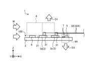
つづいて、別の各種実施形態に係る半導体モジュール1について、図5~図11を参照しながら説明する。図5は、別の実施形態1に係る半導体モジュール1の平面図である。 <Anotherembodiment 1>
Next, thesemiconductor module 1 according to various other embodiments will be described with reference to Fig. 5 to Fig. 11. Fig. 5 is a plan view of the semiconductor module 1 according to another embodiment 1.
つづいて、別の各種実施形態に係る半導体モジュール1について、図5~図11を参照しながら説明する。図5は、別の実施形態1に係る半導体モジュール1の平面図である。 <Another
Next, the
図5に示すように、別の実施形態1では、電源IC5およびチップ抵抗7の配置が、上述の実施形態と異なる。具体的には、別の実施形態1では、外側から基板2の第1面21に沿って送られる風Wに対して、すべての光素子3およびすべての電源IC5が、互いに干渉しない場所に位置してもよい。
As shown in FIG. 5, in another embodiment 1, the arrangement of the power supply ICs 5 and chip resistors 7 differs from that of the above-described embodiment. Specifically, in another embodiment 1, all of the light elements 3 and all of the power supply ICs 5 may be positioned in locations where they do not interfere with each other with respect to the wind W blown from the outside along the first surface 21 of the substrate 2.
これにより、すべての光素子3およびすべての電源IC5を、風Wによって効率よく冷却することができる。
This allows all of the optical elements 3 and all of the power supply ICs 5 to be efficiently cooled by the wind W.
また、別の実施形態1では、外側から基板2の第1面21に沿って送られる風Wに対して、チップ抵抗7が対応する電源IC5よりも風上側に位置してもよい。
In another embodiment 1, the chip resistor 7 may be positioned upwind of the corresponding power supply IC 5 with respect to the wind W blown from the outside along the first surface 21 of the substrate 2.
これにより、チップ抵抗7と、かかるチップ抵抗7よりも背の高い電源IC5との両方に風Wを当てることができる。したがって、別の実施形態1によれば、すべての電源IC5およびすべてのチップ抵抗7を、風Wによって効率よく冷却することができる。
This allows the wind W to be directed at both the chip resistors 7 and the power supply ICs 5 that are taller than the chip resistors 7. Therefore, according to another embodiment 1, all of the power supply ICs 5 and all of the chip resistors 7 can be efficiently cooled by the wind W.
また、別の実施形態1では、すべての電源IC5およびすべてのチップ抵抗7が風Wによって効率よく冷却されることで、電源IC5およびチップ抵抗7から発生する熱によって、光ファイバーケーブル32の温度が局所的に上昇することを低減できる。
In addition, in another embodiment 1, all power supply ICs 5 and all chip resistors 7 are efficiently cooled by the wind W, which reduces the local increase in temperature of the optical fiber cable 32 caused by heat generated by the power supply ICs 5 and chip resistors 7.
すなわち、別の実施形態1では、光ファイバーケーブル32の延在方向における温度分布を均一化することができる。したがって、別の実施形態1によれば、光信号の信号品質を向上させることができる。
In other words, in alternative embodiment 1, the temperature distribution in the extension direction of the optical fiber cable 32 can be made uniform. Therefore, according to alternative embodiment 1, the signal quality of the optical signal can be improved.
また、電源IC5の幅はチップ抵抗7の幅よりも広い方がよい。ここで、幅とは、基板2の第1面21に平行な方向の長さのことをいう。図5では、Y軸方向の長さになる。
Furthermore, it is preferable that the width of the power supply IC 5 is wider than the width of the chip resistor 7. Here, the width refers to the length in the direction parallel to the first surface 21 of the substrate 2. In FIG. 5, it is the length in the Y-axis direction.
電源IC5とチップ抵抗7との間で、電源IC5の幅がチップ抵抗7の幅よりも大きい(広い)場合、基板2上において、電源IC5およびチップ抵抗7を風Wの流れる方向(この場合、X軸方向)に配置したときに、幅の大きい電源IC5がチップ抵抗7の後方に配置されてもよい。
If the width of the power supply IC 5 between the power supply IC 5 and the chip resistor 7 is greater (wider) than the width of the chip resistor 7, when the power supply IC 5 and the chip resistor 7 are arranged on the substrate 2 in the direction in which the wind W flows (in this case, the X-axis direction), the wider power supply IC 5 may be arranged behind the chip resistor 7.
これは幅の広い電源IC5がチップ抵抗7の幅の分よりもはみ出た部分を有するため、電源IC5がチップ抵抗7の後方となる風Wの流れる方向の下手側に配置されても電源IC5に部分的にでも風Wが当たりやすくなるからである。
This is because the wide power supply IC 5 has a portion that extends beyond the width of the chip resistor 7, so even if the power supply IC 5 is placed downstream of the chip resistor 7 in the direction of the wind W flow, it is likely that the wind W will hit the power supply IC 5, even if only partially.
電源IC5はチップ抵抗7よりも高さ(厚み)および幅のうちの一方が大きくても良いが、高さ(厚み)および幅の両方が大きくてもよい。
The power supply IC 5 may be larger in either height (thickness) or width than the chip resistor 7, but it may also be larger in both height (thickness) and width.
<別の実施形態2>
図6は、別の実施形態2に係る半導体モジュール1の平面図である。図6に示すように、別の実施形態2では、放熱部材4の構成が上述の実施形態と異なる。具体的には、別の実施形態2では、放熱部材4が光素子3および制御IC6の上に位置するのに加え、電源IC5およびチップ抵抗7の上にも位置してもよい。 <Anotherembodiment 2>
Fig. 6 is a plan view of asemiconductor module 1 according to another embodiment 2. As shown in Fig. 6, in another embodiment 2, the configuration of the heat dissipation member 4 is different from that of the above-mentioned embodiment. Specifically, in another embodiment 2, the heat dissipation member 4 may be located not only above the optical element 3 and the control IC 6, but also above the power supply IC 5 and the chip resistor 7.
図6は、別の実施形態2に係る半導体モジュール1の平面図である。図6に示すように、別の実施形態2では、放熱部材4の構成が上述の実施形態と異なる。具体的には、別の実施形態2では、放熱部材4が光素子3および制御IC6の上に位置するのに加え、電源IC5およびチップ抵抗7の上にも位置してもよい。 <Another
Fig. 6 is a plan view of a
そして、別の実施形態2では、電源IC5およびチップ抵抗7の少なくとも一方が、放熱部材4と熱的に接続されてもよい。これにより、電源IC5およびチップ抵抗7の少なくとも一方から発生する熱を、放熱部材4によって効率よく放熱することができる。
In another embodiment 2, at least one of the power supply IC 5 and the chip resistor 7 may be thermally connected to the heat dissipation member 4. This allows the heat generated from at least one of the power supply IC 5 and the chip resistor 7 to be efficiently dissipated by the heat dissipation member 4.
また、別の実施形態2では、電源IC5及びチップ抵抗7の少なくとも一方が放熱部材4と熱的に接続されることで、電源IC5及びチップ抵抗7の少なくとも一方から発生する熱によって、光ファイバーケーブル32の温度が局所的に上昇することを低減できる。
In another embodiment 2, at least one of the power supply IC 5 and the chip resistor 7 is thermally connected to the heat dissipation member 4, thereby reducing the local increase in temperature of the optical fiber cable 32 caused by heat generated from at least one of the power supply IC 5 and the chip resistor 7.
すなわち、別の実施形態2では、光ファイバーケーブル32の延在方向における温度分布を均一化することができる。したがって、別の実施形態2によれば、光信号の信号品質を向上させることができる。
In other words, in alternative embodiment 2, the temperature distribution in the extension direction of the optical fiber cable 32 can be made uniform. Therefore, according to alternative embodiment 2, the signal quality of the optical signal can be improved.
別の実施形態2では、電源IC5またはチップ抵抗7のいずれかが放熱部材4と熱的に接続されてもよいし、電源IC5およびチップ抵抗7の両方が放熱部材4と熱的に接続されてもよい。
In another embodiment 2, either the power supply IC 5 or the chip resistor 7 may be thermally connected to the heat dissipation member 4, or both the power supply IC 5 and the chip resistor 7 may be thermally connected to the heat dissipation member 4.
電源IC5およびチップ抵抗7の両方が放熱部材4と熱的に接続されることで、電源IC5およびチップ抵抗7の両方から発生する熱を、放熱部材4によって効率よく放熱することができる。
By thermally connecting both the power supply IC 5 and the chip resistor 7 to the heat dissipation member 4, the heat generated from both the power supply IC 5 and the chip resistor 7 can be efficiently dissipated by the heat dissipation member 4.
<別の実施形態3>
図7は、別の実施形態3に係る半導体モジュール1の平面図であり、図8は、別の実施形態3に係る半導体モジュール1の側面図である。また、図9は、図7に示すA-A線の矢視断面図である。 <Anotherembodiment 3>
Fig. 7 is a plan view of thesemiconductor module 1 according to another embodiment 3, and Fig. 8 is a side view of the semiconductor module 1 according to another embodiment 3. Also, Fig. 9 is a cross-sectional view taken along line AA in Fig. 7.
図7は、別の実施形態3に係る半導体モジュール1の平面図であり、図8は、別の実施形態3に係る半導体モジュール1の側面図である。また、図9は、図7に示すA-A線の矢視断面図である。 <Another
Fig. 7 is a plan view of the
図7に示すように、別の実施形態3では、放熱部材4に加え、別の放熱部材4Aが半導体モジュール1に設けられてもよい。別の放熱部材4Aは、たとえばアルミニウム、銅、鉄などの熱伝導率が比較的高い金属で形成されてもよい。
As shown in FIG. 7, in another embodiment 3, in addition to the heat dissipation member 4, another heat dissipation member 4A may be provided on the semiconductor module 1. The other heat dissipation member 4A may be formed of a metal with a relatively high thermal conductivity, such as aluminum, copper, or iron.
別の放熱部材4Aは、図7に示すように、電源IC5およびチップ抵抗7の上に配置されてもよい。また、別の放熱部材4Aは、図9に示すように、基板2の第1面21の上方から、基板2の側面23を経由して第2面22の周縁部に回り込むように位置してもよい。
The separate heat dissipation member 4A may be disposed on top of the power supply IC 5 and the chip resistor 7, as shown in FIG. 7. The separate heat dissipation member 4A may also be positioned so as to extend from above the first surface 21 of the substrate 2, around the side surface 23 of the substrate 2, and around the periphery of the second surface 22, as shown in FIG. 9.
そして、別の実施形態3では、電源IC5およびチップ抵抗7の少なくとも一方が、別の放熱部材4Aと熱的に接続されてもよい。これにより、電源IC5およびチップ抵抗7の少なくとも一方から発生する熱を、別の放熱部材4Aによって効率よく放熱することができる。
In another embodiment 3, at least one of the power supply IC 5 and the chip resistor 7 may be thermally connected to another heat dissipation member 4A. This allows the heat generated from at least one of the power supply IC 5 and the chip resistor 7 to be efficiently dissipated by the other heat dissipation member 4A.
また、電源IC5およびチップ抵抗7の少なくとも一方が別の放熱部材4Aと熱的に接続されることで、電源IC5およびチップ抵抗7の少なくとも一方から発生する熱によって、光ファイバーケーブル32の温度が局所的に上昇することを低減できる。
In addition, by thermally connecting at least one of the power supply IC 5 and the chip resistor 7 to another heat dissipation member 4A, it is possible to reduce the local increase in temperature of the optical fiber cable 32 caused by heat generated from at least one of the power supply IC 5 and the chip resistor 7.
すなわち、別の実施形態3では、光ファイバーケーブル32の延在方向における温度分布を均一化することができる。したがって、別の実施形態3によれば、光信号の信号品質を向上させることができる。
In other words, in alternative embodiment 3, the temperature distribution in the extension direction of the optical fiber cable 32 can be made uniform. Therefore, according to alternative embodiment 3, the signal quality of the optical signal can be improved.
また、別の実施形態3では、図8に示すように、別の放熱部材4Aが放熱する第3方向D3が、放熱部材4が放熱する第1方向D1と異なる向きであってもよい。たとえば、放熱部材4が放熱する第1方向D1はZ軸正方向であり、別の放熱部材4Aが放熱する第3方向D3はZ軸負方向であってもよい。
In another embodiment 3, as shown in FIG. 8, the third direction D3 in which the separate heat dissipation member 4A dissipates heat may be oriented in a direction different from the first direction D1 in which the heat dissipation member 4 dissipates heat. For example, the first direction D1 in which the heat dissipation member 4 dissipates heat may be the positive direction of the Z axis, and the third direction D3 in which the separate heat dissipation member 4A dissipates heat may be the negative direction of the Z axis.
これにより、基板2の第1面21に位置する光素子3、電源IC5、制御IC6およびチップ抵抗7をさらに効率よく冷却することができる。
This allows the optical element 3, power supply IC 5, control IC 6 and chip resistor 7 located on the first surface 21 of the substrate 2 to be cooled even more efficiently.
また、別の実施形態3では、別の放熱部材4Aが放熱する第3方向D3を基板2の第2面22側に向けることで、電源IC5およびチップ抵抗7の少なくとも一方から発生する熱によって、光ファイバーケーブル32の温度が局所的に上昇することを低減できる。
In addition, in another embodiment 3, the third direction D3 in which the other heat dissipation member 4A dissipates heat is directed toward the second surface 22 of the substrate 2, thereby reducing the local increase in temperature of the optical fiber cable 32 caused by heat generated from at least one of the power supply IC 5 and the chip resistor 7.
すなわち、別の実施形態3では、光ファイバーケーブル32の延在方向における温度分布を均一化することができる。したがって、別の実施形態3によれば、光信号の信号品質を向上させることができる。
In other words, in alternative embodiment 3, the temperature distribution in the extension direction of the optical fiber cable 32 can be made uniform. Therefore, according to alternative embodiment 3, the signal quality of the optical signal can be improved.
また、別の実施形態3では、図9に示すように、別の放熱部材4Aと光ファイバーケーブル32とを互いに離間させてもよい。これにより、別の放熱部材4Aから光ファイバーケーブル32への熱の伝達を低減することができるため、光ファイバーケーブル32の延在方向における温度分布を均一化することができる。
In another embodiment 3, as shown in FIG. 9, the separate heat dissipation member 4A and the optical fiber cable 32 may be spaced apart from each other. This reduces the transfer of heat from the separate heat dissipation member 4A to the optical fiber cable 32, making it possible to homogenize the temperature distribution in the extension direction of the optical fiber cable 32.
したがって、別の実施形態3によれば、光信号の信号品質を向上させることができる。
Therefore, according to another embodiment 3, the signal quality of the optical signal can be improved.
なお、別の実施形態3では、別の放熱部材4Aと光ファイバーケーブル32との間に断熱部材が位置してもよい。これによっても、別の放熱部材4Aから光ファイバーケーブル32への熱の伝達を低減することができる。
In addition, in another embodiment 3, a heat insulating member may be positioned between the other heat dissipation member 4A and the optical fiber cable 32. This also makes it possible to reduce the transfer of heat from the other heat dissipation member 4A to the optical fiber cable 32.
また、別の実施形態3では、図9に示すように、別の放熱部材4Aが断面視で略C字形状を有してもよい。これにより、基板2の上方から別の放熱部材4Aを嵌め込むように、別の放熱部材4Aを基板2に固定することができる。
In another embodiment 3, as shown in FIG. 9, the separate heat dissipation member 4A may have a substantially C-shape in cross section. This allows the separate heat dissipation member 4A to be fixed to the substrate 2 by fitting the separate heat dissipation member 4A from above the substrate 2.
したがって、別の実施形態3によれば、別の放熱部材4Aを基板2に簡便に取り付けることができる。
Therefore, according to another embodiment 3, another heat dissipation member 4A can be easily attached to the substrate 2.
<別の実施形態4>
図10は、別の実施形態4に係る半導体モジュール1を斜め上方から見た斜視図であり、図11は、図10に示すB-B線の矢視断面図である。 <Anotherembodiment 4>
FIG. 10 is a perspective view of asemiconductor module 1 according to another embodiment 4, as viewed obliquely from above, and FIG. 11 is a cross-sectional view taken along line BB in FIG.
図10は、別の実施形態4に係る半導体モジュール1を斜め上方から見た斜視図であり、図11は、図10に示すB-B線の矢視断面図である。 <Another
FIG. 10 is a perspective view of a
図10および図11に示すように、別の実施形態4では、放熱部材4における第2部45の構成が上述の実施形態(図1参照)と異なる。具体的には、別の実施形態4では、第2部45が第1部41から第1方向D1に沿って延びる板状の放熱フィンであってもよい。
As shown in Figures 10 and 11, in another embodiment 4, the configuration of the second portion 45 of the heat dissipation member 4 differs from that of the above-described embodiment (see Figure 1). Specifically, in another embodiment 4, the second portion 45 may be a plate-shaped heat dissipation fin extending from the first portion 41 along the first direction D1.
別の実施形態4では、たとえば、図11に示すように、複数の第2部45が、第2方向D2(図10参照)と交差する第4方向D4(たとえば、Y軸方向)に沿って、互いに第2間隔G2をあけて位置する。
In another embodiment 4, for example, as shown in FIG. 11, multiple second portions 45 are positioned at a second interval G2 from each other along a fourth direction D4 (e.g., the Y-axis direction) that intersects with the second direction D2 (see FIG. 10).
これにより、第2部45が放熱ピンである場合と比べて、第2部45の第4方向D4における寸法S1を小さくできるため、放熱部材4を軽量化することができる。
As a result, the dimension S1 of the second portion 45 in the fourth direction D4 can be made smaller than when the second portion 45 is a heat dissipation pin, making it possible to reduce the weight of the heat dissipation member 4.
また、別の実施形態4では、図10に示すように、隣接する第2部45同士の間の第2間隔G2(図11参照)が、第2方向D2に沿って延びてもよい。これにより、送風機(図示せず)から送られた風W(図3参照)が第2間隔G2に沿ってスムーズに流れるため、風Wがすべての第2部45に略均等に当たる。
In another embodiment 4, as shown in FIG. 10, the second gap G2 (see FIG. 11) between adjacent second portions 45 may extend along the second direction D2. This allows the wind W (see FIG. 3) sent from a blower (not shown) to flow smoothly along the second gap G2, so that the wind W hits all of the second portions 45 approximately evenly.
したがって、別の実施形態4によれば、放熱部材4の放熱効率をさらに高めることができる。
Therefore, according to another embodiment 4, the heat dissipation efficiency of the heat dissipation member 4 can be further improved.
また、別の実施形態4では、図11に示すように、第2部45の第4方向D4における寸法S1が、第3部42の第4方向D4における寸法S2よりも小さくてもよい。このように、第2部45の寸法S1を小さくする(すなわち、第2部45を薄くする)ことで、放熱部材4を小型低背化したとしても、所望の放熱効率を実現することができる。
In another embodiment 4, as shown in FIG. 11, the dimension S1 of the second portion 45 in the fourth direction D4 may be smaller than the dimension S2 of the third portion 42 in the fourth direction D4. In this way, by reducing the dimension S1 of the second portion 45 (i.e., making the second portion 45 thinner), the desired heat dissipation efficiency can be achieved even if the heat dissipation member 4 is made smaller and thinner.
すなわち、別の実施形態4では、第2部45の寸法S1を第3部42の寸法S2よりも小さくすることで、第3部42の太さを確保して放熱部材4を基板2に安定して固定することができるとともに、第2部45を細くして放熱部材4の小型低背化を実現することができる。なお、本開示において、第2部45の第4方向D4における寸法S1は、たとえば、0.5mm~1.0mmであってもよく、より具体的には0.6mm程度である。第3部42の寸法S2は、たとえば、1mm以上であってもよい。
In other words, in another embodiment 4, by making the dimension S1 of the second portion 45 smaller than the dimension S2 of the third portion 42, the thickness of the third portion 42 can be ensured to stably fix the heat dissipation member 4 to the substrate 2, and the second portion 45 can be made thinner to achieve a smaller and lower-profile heat dissipation member 4. Note that in the present disclosure, the dimension S1 of the second portion 45 in the fourth direction D4 may be, for example, 0.5 mm to 1.0 mm, and more specifically, is approximately 0.6 mm. The dimension S2 of the third portion 42 may be, for example, 1 mm or more.
また、別の実施形態4では、第2間隔G2の第4方向D4における寸法をS3とした場合に、インタフェース部31の第4方向D4における寸法S4が、以下の式(1)を満たしていてもよい。
S4≧2×S1+2×S3 ・・・(1) In anotherembodiment 4, when the dimension of the second gap G2 in the fourth direction D4 is S3, the dimension S4 of the interface portion 31 in the fourth direction D4 may satisfy the following formula (1).
S4≧2×S1+2×S3 (1)
S4≧2×S1+2×S3 ・・・(1) In another
S4≧2×S1+2×S3 (1)
換言すると、インタフェース部31の第4方向D4における寸法S4を基準にして、第2部45の厚み(すなわち、寸法S1)だけでなく、複数の第2部45のピッチ(すなわち、寸法S3)も小さくするように、放熱部材4の寸法が規定されるとよい。
In other words, the dimensions of the heat dissipation member 4 should be specified so that not only the thickness of the second portion 45 (i.e., dimension S1) but also the pitch between the multiple second portions 45 (i.e., dimension S3) is small, based on the dimension S4 in the fourth direction D4 of the interface portion 31.
これにより、第1部41の上面に配置できる第2部45の数を増やすことができるため、放熱部材4の放熱効率をさらに高めることができる。また、放熱部材4を小型低背化したとしても所望の放熱効率を実現することができるため、放熱部材4の小型低背化を実現することができる。
This allows the number of second sections 45 that can be placed on the top surface of the first section 41 to be increased, further improving the heat dissipation efficiency of the heat dissipation member 4. In addition, the desired heat dissipation efficiency can be achieved even if the heat dissipation member 4 is made small and low-profile, so the heat dissipation member 4 can be made small and low-profile.
以上、本開示の実施形態について説明したが、本開示は上記実施形態に限定されるものではなく、その趣旨を逸脱しない限りにおいて種々の変更が可能である。
The above describes an embodiment of the present disclosure, but the present disclosure is not limited to the above embodiment, and various modifications are possible without departing from the spirit of the present disclosure.
さらなる効果や他の態様は、当業者によって容易に導き出すことができる。このため、本開示のより広範な態様は、以上のように表しかつ記述した特定の詳細および代表的な実施形態に限定されるものではない。したがって、添付の請求の範囲およびその均等物によって定義される総括的な発明の概念の精神または範囲から逸脱することなく、様々な変更が可能である。
Further advantages and other aspects may readily occur to those skilled in the art. Thus, the disclosure in its broader aspects is not limited to the specific details and representative embodiments shown and described above. Accordingly, various modifications may be made without departing from the spirit or scope of the general inventive concept as defined by the appended claims and equivalents thereof.
なお、本技術は以下のような構成も取ることができる。
(1)
基板と、
前記基板の第1面に位置する少なくとも1つの半導体素子と、
前記半導体素子の上方に位置する放熱部材と、
前記半導体素子に接続される光ファイバーケーブルと、
を備え、
前記半導体素子に対して前記放熱部材が延びる第1方向と、前記光ファイバーケーブルが延びる第2方向とが交差する
半導体モジュール。
(2)
前記光ファイバーケーブルは、少なくとも前記基板の上方において前記第1面に平行な部分を有する
前記(1)に記載の半導体モジュール。
(3)
前記第1面に位置し、前記半導体素子に電力を供給する少なくとも1つの電源ICと、
前記第1面に位置し、前記電源ICに電気的に接続される少なくとも1つのチップ抵抗と、
をさらに備え、
前記電源ICおよび前記チップ抵抗の少なくとも一方は、前記第1面を平面視した場合に、前記光ファイバーケーブルに隣接し、かつ前記光ファイバーケーブルと重ならない場所に位置する
前記(1)または(2)に記載の半導体モジュール。
(4)
外側から前記基板の前記第1面に沿って送られる風に対して、前記半導体素子および前記電源ICが、互いに干渉しない場所に位置する
前記(3)に記載の半導体モジュール。
(5)
外側から前記基板の前記第1面に沿って送られる風に対して、前記チップ抵抗が前記電源ICよりも風上側に位置する
前記(3)または(4)に記載の半導体モジュール。
(6)
前記電源ICおよび前記チップ抵抗の少なくとも一方は、前記放熱部材と熱的に接続される
前記(3)~(5)のいずれか一つに記載の半導体モジュール。
(7)
前記電源ICおよび前記チップ抵抗の少なくとも一方は、別の放熱部材と熱的に接続される
前記(3)~(5)のいずれか一つに記載の半導体モジュール。
(8)
前記別の放熱部材が放熱する第3方向は、前記第1方向と異なる向きである
前記(7)に記載の半導体モジュール。
(9)
前記放熱部材は、少なくとも、前記基板と第1間隔をあけて且つ前記基板に対向して位置する板状の第1部と、該第1部から前記第1方向に沿って延びる複数の第2部と、を有しており、
前記第2部は、前記第1方向に沿って延びる板状の放熱フィンである
前記(1)~(8)のいずれか一つに記載の半導体モジュール。
(10)
複数の前記第2部は、前記第2方向と交差する第4方向に沿って、互いに第2間隔をあけて位置するとともに、
前記第2間隔は、前記第2方向に沿って延びる
前記(9)に記載の半導体モジュール。
(11)
前記放熱部材は、前記第1部から前記基板に向かって延びて前記基板と接するとともに、前記第4方向に沿って互いに第3間隔をあけて位置する複数の第3部をさらに有しており、
前記第2部の前記第4方向における寸法は、前記第3部の前記第4方向における寸法よりも小さい
前記(10)に記載の半導体モジュール。 The present technology can also be configured as follows.
(1)
A substrate;
at least one semiconductor device located on a first surface of the substrate;
a heat dissipation member located above the semiconductor element;
an optical fiber cable connected to the semiconductor device;
Equipped with
a first direction in which the heat dissipation member extends relative to the semiconductor element and a second direction in which the optical fiber cable extends intersect with each other.
(2)
The semiconductor module according to (1), wherein the optical fiber cable has at least a portion parallel to the first surface above the substrate.
(3)
At least one power supply IC located on the first surface and supplying power to the semiconductor device;
at least one chip resistor located on the first surface and electrically connected to the power supply IC;
Further equipped with
The semiconductor module described in (1) or (2), wherein at least one of the power supply IC and the chip resistor is located adjacent to the optical fiber cable and does not overlap with the optical fiber cable when viewed in a planar view of the first surface.
(4)
The semiconductor module according to (3), wherein the semiconductor element and the power supply IC are positioned so as not to interfere with each other with respect to wind blown from the outside along the first surface of the substrate.
(5)
The semiconductor module according to (3) or (4), wherein the chip resistor is located on the windward side of the power supply IC with respect to wind blown from the outside along the first surface of the substrate.
(6)
At least one of the power supply IC and the chip resistor is thermally connected to the heat dissipation member.
(7)
At least one of the power supply IC and the chip resistor is thermally connected to another heat dissipation member.
(8)
The semiconductor module according to (7), wherein a third direction in which the another heat dissipation member dissipates heat is different from the first direction.
(9)
the heat dissipation member has at least a plate-like first portion positioned opposite the substrate with a first distance therebetween, and a plurality of second portions extending from the first portion along the first direction,
The semiconductor module according to any one of (1) to (8), wherein the second portion is a plate-shaped heat dissipation fin extending along the first direction.
(10)
The second portions are positioned at second intervals from each other along a fourth direction intersecting the second direction,
The semiconductor module according to (9), wherein the second interval extends along the second direction.
(11)
the heat dissipation member further includes a plurality of third portions extending from the first portion toward the substrate and in contact with the substrate, the third portions being spaced apart from each other along the fourth direction,
The semiconductor module according to (10), wherein a dimension of the second portion in the fourth direction is smaller than a dimension of the third portion in the fourth direction.
(1)
基板と、
前記基板の第1面に位置する少なくとも1つの半導体素子と、
前記半導体素子の上方に位置する放熱部材と、
前記半導体素子に接続される光ファイバーケーブルと、
を備え、
前記半導体素子に対して前記放熱部材が延びる第1方向と、前記光ファイバーケーブルが延びる第2方向とが交差する
半導体モジュール。
(2)
前記光ファイバーケーブルは、少なくとも前記基板の上方において前記第1面に平行な部分を有する
前記(1)に記載の半導体モジュール。
(3)
前記第1面に位置し、前記半導体素子に電力を供給する少なくとも1つの電源ICと、
前記第1面に位置し、前記電源ICに電気的に接続される少なくとも1つのチップ抵抗と、
をさらに備え、
前記電源ICおよび前記チップ抵抗の少なくとも一方は、前記第1面を平面視した場合に、前記光ファイバーケーブルに隣接し、かつ前記光ファイバーケーブルと重ならない場所に位置する
前記(1)または(2)に記載の半導体モジュール。
(4)
外側から前記基板の前記第1面に沿って送られる風に対して、前記半導体素子および前記電源ICが、互いに干渉しない場所に位置する
前記(3)に記載の半導体モジュール。
(5)
外側から前記基板の前記第1面に沿って送られる風に対して、前記チップ抵抗が前記電源ICよりも風上側に位置する
前記(3)または(4)に記載の半導体モジュール。
(6)
前記電源ICおよび前記チップ抵抗の少なくとも一方は、前記放熱部材と熱的に接続される
前記(3)~(5)のいずれか一つに記載の半導体モジュール。
(7)
前記電源ICおよび前記チップ抵抗の少なくとも一方は、別の放熱部材と熱的に接続される
前記(3)~(5)のいずれか一つに記載の半導体モジュール。
(8)
前記別の放熱部材が放熱する第3方向は、前記第1方向と異なる向きである
前記(7)に記載の半導体モジュール。
(9)
前記放熱部材は、少なくとも、前記基板と第1間隔をあけて且つ前記基板に対向して位置する板状の第1部と、該第1部から前記第1方向に沿って延びる複数の第2部と、を有しており、
前記第2部は、前記第1方向に沿って延びる板状の放熱フィンである
前記(1)~(8)のいずれか一つに記載の半導体モジュール。
(10)
複数の前記第2部は、前記第2方向と交差する第4方向に沿って、互いに第2間隔をあけて位置するとともに、
前記第2間隔は、前記第2方向に沿って延びる
前記(9)に記載の半導体モジュール。
(11)
前記放熱部材は、前記第1部から前記基板に向かって延びて前記基板と接するとともに、前記第4方向に沿って互いに第3間隔をあけて位置する複数の第3部をさらに有しており、
前記第2部の前記第4方向における寸法は、前記第3部の前記第4方向における寸法よりも小さい
前記(10)に記載の半導体モジュール。 The present technology can also be configured as follows.
(1)
A substrate;
at least one semiconductor device located on a first surface of the substrate;
a heat dissipation member located above the semiconductor element;
an optical fiber cable connected to the semiconductor device;
Equipped with
a first direction in which the heat dissipation member extends relative to the semiconductor element and a second direction in which the optical fiber cable extends intersect with each other.
(2)
The semiconductor module according to (1), wherein the optical fiber cable has at least a portion parallel to the first surface above the substrate.
(3)
At least one power supply IC located on the first surface and supplying power to the semiconductor device;
at least one chip resistor located on the first surface and electrically connected to the power supply IC;
Further equipped with
The semiconductor module described in (1) or (2), wherein at least one of the power supply IC and the chip resistor is located adjacent to the optical fiber cable and does not overlap with the optical fiber cable when viewed in a planar view of the first surface.
(4)
The semiconductor module according to (3), wherein the semiconductor element and the power supply IC are positioned so as not to interfere with each other with respect to wind blown from the outside along the first surface of the substrate.
(5)
The semiconductor module according to (3) or (4), wherein the chip resistor is located on the windward side of the power supply IC with respect to wind blown from the outside along the first surface of the substrate.
(6)
At least one of the power supply IC and the chip resistor is thermally connected to the heat dissipation member.
(7)
At least one of the power supply IC and the chip resistor is thermally connected to another heat dissipation member.
(8)
The semiconductor module according to (7), wherein a third direction in which the another heat dissipation member dissipates heat is different from the first direction.
(9)
the heat dissipation member has at least a plate-like first portion positioned opposite the substrate with a first distance therebetween, and a plurality of second portions extending from the first portion along the first direction,
The semiconductor module according to any one of (1) to (8), wherein the second portion is a plate-shaped heat dissipation fin extending along the first direction.
(10)
The second portions are positioned at second intervals from each other along a fourth direction intersecting the second direction,
The semiconductor module according to (9), wherein the second interval extends along the second direction.
(11)
the heat dissipation member further includes a plurality of third portions extending from the first portion toward the substrate and in contact with the substrate, the third portions being spaced apart from each other along the fourth direction,
The semiconductor module according to (10), wherein a dimension of the second portion in the fourth direction is smaller than a dimension of the third portion in the fourth direction.
1 半導体モジュール
2 基板
21 第1面
3、3a~3d 光素子(半導体素子の一例)
32 光ファイバーケーブル
4 放熱部材
41 第1部
42 第3部
45 第2部
4A 別の放熱部材
5 電源IC
6 制御IC
7 チップ抵抗
D1 第1方向
D2 第2方向
D3 第3方向
D4 第4方向
G1 第1間隔
G2 第2間隔
G3 第3間隔
S1~S4 寸法
W 風1 Semiconductor module 2 Substrate 21 First surface 3, 3a to 3d Optical element (an example of a semiconductor element)
32Optical fiber cable 4 Heat dissipation member 41 First part 42 Third part 45 Second part 4A Another heat dissipation member 5 Power supply IC
6 Control IC
7 Chip resistance D1 First direction D2 Second direction D3 Third direction D4 Fourth direction G1 First interval G2 Second interval G3 Third interval S1 to S4 Dimensions W Wind
2 基板
21 第1面
3、3a~3d 光素子(半導体素子の一例)
32 光ファイバーケーブル
4 放熱部材
41 第1部
42 第3部
45 第2部
4A 別の放熱部材
5 電源IC
6 制御IC
7 チップ抵抗
D1 第1方向
D2 第2方向
D3 第3方向
D4 第4方向
G1 第1間隔
G2 第2間隔
G3 第3間隔
S1~S4 寸法
W 風
32
6 Control IC
7 Chip resistance D1 First direction D2 Second direction D3 Third direction D4 Fourth direction G1 First interval G2 Second interval G3 Third interval S1 to S4 Dimensions W Wind
Claims (11)
- 基板と、
前記基板の第1面に位置する少なくとも1つの半導体素子と、
前記半導体素子の上方に位置する放熱部材と、
前記半導体素子に接続される光ファイバーケーブルと、
を備え、
前記半導体素子に対して前記放熱部材が延びる第1方向と、前記光ファイバーケーブルが延びる第2方向とが交差する
半導体モジュール。 A substrate;
at least one semiconductor device located on a first surface of the substrate;
a heat dissipation member located above the semiconductor element;
an optical fiber cable connected to the semiconductor device;
Equipped with
a first direction in which the heat dissipation member extends relative to the semiconductor element and a second direction in which the optical fiber cable extends intersect with each other. - 前記光ファイバーケーブルは、少なくとも前記基板の上方において前記第1面に平行な部分を有する
請求項1に記載の半導体モジュール。 The semiconductor module according to claim 1 , wherein the optical fiber cable has at least a portion parallel to the first surface above the substrate. - 前記第1面に位置し、前記半導体素子に電力を供給する少なくとも1つの電源ICと、
前記第1面に位置し、前記電源ICに電気的に接続される少なくとも1つのチップ抵抗と、
をさらに備え、
前記電源ICおよび前記チップ抵抗の少なくとも一方は、前記第1面を平面視した場合に、前記光ファイバーケーブルに隣接し、かつ前記光ファイバーケーブルと重ならない場所に位置する
請求項1または2に記載の半導体モジュール。 At least one power supply IC located on the first surface and supplying power to the semiconductor device;
at least one chip resistor located on the first surface and electrically connected to the power supply IC;
Further equipped with
The semiconductor module according to claim 1 , wherein at least one of the power supply IC and the chip resistor is located adjacent to the optical fiber cable but does not overlap with the optical fiber cable when the first surface is viewed in a plan view. - 外側から前記基板の前記第1面に沿って送られる風に対して、前記半導体素子および前記電源ICが、互いに干渉しない場所に位置する
請求項3に記載の半導体モジュール。 The semiconductor module according to claim 3 , wherein the semiconductor element and the power supply IC are positioned so as not to interfere with each other with respect to wind blown from the outside along the first surface of the substrate. - 外側から前記基板の前記第1面に沿って送られる風に対して、前記チップ抵抗が前記電源ICよりも風上側に位置する
請求項3または4に記載の半導体モジュール。 5. The semiconductor module according to claim 3, wherein the chip resistor is located on an upwind side of the power supply IC with respect to a wind blown from the outside along the first surface of the substrate. - 前記電源ICおよび前記チップ抵抗の少なくとも一方は、前記放熱部材と熱的に接続される
請求項3~5のいずれか一つに記載の半導体モジュール。 6. The semiconductor module according to claim 3, wherein at least one of the power supply IC and the chip resistor is thermally connected to the heat dissipation member. - 前記電源ICおよび前記チップ抵抗の少なくとも一方は、別の放熱部材と熱的に接続される
請求項3~5のいずれか一つに記載の半導体モジュール。 6. The semiconductor module according to claim 3, wherein at least one of the power supply IC and the chip resistor is thermally connected to another heat dissipation member. - 前記別の放熱部材が放熱する第3方向は、前記第1方向と異なる向きである
請求項7に記載の半導体モジュール。 The semiconductor module according to claim 7 , wherein a third direction in which the another heat dissipation member dissipates heat is different from the first direction. - 前記放熱部材は、少なくとも、前記基板と第1間隔をあけて且つ前記基板に対向して位置する板状の第1部と、該第1部から前記第1方向に沿って延びる複数の第2部と、を有しており、
前記第2部は、前記第1方向に沿って延びる板状の放熱フィンである
請求項1~8のいずれか一つに記載の半導体モジュール。 the heat dissipation member has at least a plate-like first portion positioned opposite the substrate with a first distance therebetween, and a plurality of second portions extending from the first portion along the first direction,
9. The semiconductor module according to claim 1, wherein the second portion is a plate-shaped heat dissipation fin extending along the first direction. - 複数の前記第2部は、前記第2方向と交差する第4方向に沿って、互いに第2間隔をあけて位置するとともに、
前記第2間隔は、前記第2方向に沿って延びる
請求項9に記載の半導体モジュール。 The second portions are positioned at second intervals from each other along a fourth direction intersecting the second direction,
The semiconductor module according to claim 9 , wherein the second interval extends along the second direction. - 前記放熱部材は、前記第1部から前記基板に向かって延びて前記基板と接するとともに、前記第4方向に沿って互いに第3間隔をあけて位置する複数の第3部をさらに有しており、
前記第2部の前記第4方向における寸法は、前記第3部の前記第4方向における寸法よりも小さい
請求項10に記載の半導体モジュール。 the heat dissipation member further includes a plurality of third portions extending from the first portion toward the substrate and in contact with the substrate, the third portions being spaced apart from each other along the fourth direction,
The semiconductor module according to claim 10 , wherein a dimension of the second portion in the fourth direction is smaller than a dimension of the third portion in the fourth direction.
Applications Claiming Priority (2)
| Application Number | Priority Date | Filing Date | Title |
|---|---|---|---|
| JP2022-152741 | 2022-09-26 | ||
| JP2022152741 | 2022-09-26 |
Publications (1)
| Publication Number | Publication Date |
|---|---|
| WO2024071110A1 true WO2024071110A1 (en) | 2024-04-04 |
Family
ID=90478003
Family Applications (1)
| Application Number | Title | Priority Date | Filing Date |
|---|---|---|---|
| PCT/JP2023/034917 WO2024071110A1 (en) | 2022-09-26 | 2023-09-26 | Semiconductor module |
Country Status (1)
| Country | Link |
|---|---|
| WO (1) | WO2024071110A1 (en) |
Citations (6)
| Publication number | Priority date | Publication date | Assignee | Title |
|---|---|---|---|---|
| JP2001007403A (en) * | 1999-06-23 | 2001-01-12 | Nec Corp | Parallel transmission type of optical module, and its manufacture |
| JP2005064384A (en) * | 2003-08-19 | 2005-03-10 | Toshiba Corp | Lsi package with interface module and heat sink used for it |
| JP2010211157A (en) * | 2009-03-12 | 2010-09-24 | Hitachi Cable Ltd | Optical transmitter-receiver |
| JP2014178383A (en) * | 2013-03-13 | 2014-09-25 | Hitachi Metals Ltd | Communication module and signal transmission device provided with the same |
| JP2015084040A (en) * | 2013-10-25 | 2015-04-30 | 日立金属株式会社 | Optical communication module |
| JP2016031990A (en) * | 2014-07-28 | 2016-03-07 | 日立金属株式会社 | Photo-electric conversion module and transmission device including photo-electric conversion module |
-
2023
- 2023-09-26 WO PCT/JP2023/034917 patent/WO2024071110A1/en unknown
Patent Citations (6)
| Publication number | Priority date | Publication date | Assignee | Title |
|---|---|---|---|---|
| JP2001007403A (en) * | 1999-06-23 | 2001-01-12 | Nec Corp | Parallel transmission type of optical module, and its manufacture |
| JP2005064384A (en) * | 2003-08-19 | 2005-03-10 | Toshiba Corp | Lsi package with interface module and heat sink used for it |
| JP2010211157A (en) * | 2009-03-12 | 2010-09-24 | Hitachi Cable Ltd | Optical transmitter-receiver |
| JP2014178383A (en) * | 2013-03-13 | 2014-09-25 | Hitachi Metals Ltd | Communication module and signal transmission device provided with the same |
| JP2015084040A (en) * | 2013-10-25 | 2015-04-30 | 日立金属株式会社 | Optical communication module |
| JP2016031990A (en) * | 2014-07-28 | 2016-03-07 | 日立金属株式会社 | Photo-electric conversion module and transmission device including photo-electric conversion module |
Similar Documents
| Publication | Publication Date | Title |
|---|---|---|
| US7898806B2 (en) | Motor controller | |
| JP5082970B2 (en) | Circuit board equipment | |
| TWI527168B (en) | Cooling apparatus and power module with cooling apparatus using the same | |
| JPH07283564A (en) | Electronic device | |
| US7957143B2 (en) | Motor controller | |
| JP2010187504A (en) | Inverter device | |
| JP2001119181A (en) | Cooling unit for electronic component and electronic apparatus | |
| CN102754202A (en) | Heat radiation device and electronic equipment using the same | |
| JP7339075B2 (en) | Electrical equipment, electronic controller | |
| CN113597823B (en) | Electronic control device | |
| WO2024083242A1 (en) | Working assembly and electronic device | |
| WO2024071110A1 (en) | Semiconductor module | |
| US20220361372A1 (en) | Heatsink with increased air flow | |
| CN114396662A (en) | Electric control box and air conditioner outdoor unit with same | |
| JP2018198508A (en) | Power semiconductor device and electric power conversion system | |
| JP6222938B2 (en) | Heat dissipation device | |
| WO2024071190A1 (en) | Semiconductor module | |
| JP4403753B2 (en) | Power converter | |
| WO2023145964A1 (en) | Semiconductor module | |
| WO2023100480A1 (en) | Electronic control device | |
| JPH10256766A (en) | Forced air cooling structure for electronic apparatus | |
| CN209914352U (en) | Radiating fin and radiating device using same | |
| US20080068794A1 (en) | Dissipation module and electronic device having the same | |
| CN220439616U (en) | Power device module and driver | |
| CN215220704U (en) | Heat dissipation part and electronic device |