WO2024048270A1 - 導電膜の製造方法、分散液、感放射線性樹脂組成物、発光素子 - Google Patents
導電膜の製造方法、分散液、感放射線性樹脂組成物、発光素子 Download PDFInfo
- Publication number
- WO2024048270A1 WO2024048270A1 PCT/JP2023/029520 JP2023029520W WO2024048270A1 WO 2024048270 A1 WO2024048270 A1 WO 2024048270A1 JP 2023029520 W JP2023029520 W JP 2023029520W WO 2024048270 A1 WO2024048270 A1 WO 2024048270A1
- Authority
- WO
- WIPO (PCT)
- Prior art keywords
- conductive film
- polymer
- radiation
- resin composition
- sensitive resin
- Prior art date
- Legal status (The legal status is an assumption and is not a legal conclusion. Google has not performed a legal analysis and makes no representation as to the accuracy of the status listed.)
- Ceased
Links
Images




Classifications
-
- B—PERFORMING OPERATIONS; TRANSPORTING
- B05—SPRAYING OR ATOMISING IN GENERAL; APPLYING FLUENT MATERIALS TO SURFACES, IN GENERAL
- B05D—PROCESSES FOR APPLYING FLUENT MATERIALS TO SURFACES, IN GENERAL
- B05D1/00—Processes for applying liquids or other fluent materials
- B05D1/36—Successively applying liquids or other fluent materials, e.g. without intermediate treatment
-
- B—PERFORMING OPERATIONS; TRANSPORTING
- B05—SPRAYING OR ATOMISING IN GENERAL; APPLYING FLUENT MATERIALS TO SURFACES, IN GENERAL
- B05D—PROCESSES FOR APPLYING FLUENT MATERIALS TO SURFACES, IN GENERAL
- B05D3/00—Pretreatment of surfaces to which liquids or other fluent materials are to be applied; After-treatment of applied coatings, e.g. intermediate treating of an applied coating preparatory to subsequent applications of liquids or other fluent materials
- B05D3/06—Pretreatment of surfaces to which liquids or other fluent materials are to be applied; After-treatment of applied coatings, e.g. intermediate treating of an applied coating preparatory to subsequent applications of liquids or other fluent materials by exposure to radiation
-
- B—PERFORMING OPERATIONS; TRANSPORTING
- B05—SPRAYING OR ATOMISING IN GENERAL; APPLYING FLUENT MATERIALS TO SURFACES, IN GENERAL
- B05D—PROCESSES FOR APPLYING FLUENT MATERIALS TO SURFACES, IN GENERAL
- B05D3/00—Pretreatment of surfaces to which liquids or other fluent materials are to be applied; After-treatment of applied coatings, e.g. intermediate treating of an applied coating preparatory to subsequent applications of liquids or other fluent materials
- B05D3/10—Pretreatment of surfaces to which liquids or other fluent materials are to be applied; After-treatment of applied coatings, e.g. intermediate treating of an applied coating preparatory to subsequent applications of liquids or other fluent materials by other chemical means
-
- B—PERFORMING OPERATIONS; TRANSPORTING
- B05—SPRAYING OR ATOMISING IN GENERAL; APPLYING FLUENT MATERIALS TO SURFACES, IN GENERAL
- B05D—PROCESSES FOR APPLYING FLUENT MATERIALS TO SURFACES, IN GENERAL
- B05D5/00—Processes for applying liquids or other fluent materials to surfaces to obtain special surface effects, finishes or structures
- B05D5/12—Processes for applying liquids or other fluent materials to surfaces to obtain special surface effects, finishes or structures to obtain a coating with specific electrical properties
-
- B—PERFORMING OPERATIONS; TRANSPORTING
- B05—SPRAYING OR ATOMISING IN GENERAL; APPLYING FLUENT MATERIALS TO SURFACES, IN GENERAL
- B05D—PROCESSES FOR APPLYING FLUENT MATERIALS TO SURFACES, IN GENERAL
- B05D7/00—Processes, other than flocking, specially adapted for applying liquids or other fluent materials to particular surfaces or for applying particular liquids or other fluent materials
- B05D7/24—Processes, other than flocking, specially adapted for applying liquids or other fluent materials to particular surfaces or for applying particular liquids or other fluent materials for applying particular liquids or other fluent materials
-
- C—CHEMISTRY; METALLURGY
- C09—DYES; PAINTS; POLISHES; NATURAL RESINS; ADHESIVES; COMPOSITIONS NOT OTHERWISE PROVIDED FOR; APPLICATIONS OF MATERIALS NOT OTHERWISE PROVIDED FOR
- C09D—COATING COMPOSITIONS, e.g. PAINTS, VARNISHES OR LACQUERS; FILLING PASTES; CHEMICAL PAINT OR INK REMOVERS; INKS; CORRECTING FLUIDS; WOODSTAINS; PASTES OR SOLIDS FOR COLOURING OR PRINTING; USE OF MATERIALS THEREFOR
- C09D179/00—Coating compositions based on macromolecular compounds obtained by reactions forming in the main chain of the macromolecule a linkage containing nitrogen, with or without oxygen, or carbon only, not provided for in groups C09D161/00 - C09D177/00
- C09D179/04—Polycondensates having nitrogen-containing heterocyclic rings in the main chain; Polyhydrazides; Polyamide acids or similar polyimide precursors
- C09D179/08—Polyimides; Polyester-imides; Polyamide-imides; Polyamide acids or similar polyimide precursors
-
- C—CHEMISTRY; METALLURGY
- C09—DYES; PAINTS; POLISHES; NATURAL RESINS; ADHESIVES; COMPOSITIONS NOT OTHERWISE PROVIDED FOR; APPLICATIONS OF MATERIALS NOT OTHERWISE PROVIDED FOR
- C09D—COATING COMPOSITIONS, e.g. PAINTS, VARNISHES OR LACQUERS; FILLING PASTES; CHEMICAL PAINT OR INK REMOVERS; INKS; CORRECTING FLUIDS; WOODSTAINS; PASTES OR SOLIDS FOR COLOURING OR PRINTING; USE OF MATERIALS THEREFOR
- C09D5/00—Coating compositions, e.g. paints, varnishes or lacquers, characterised by their physical nature or the effects produced; Filling pastes
- C09D5/24—Electrically-conducting paints
-
- H—ELECTRICITY
- H05—ELECTRIC TECHNIQUES NOT OTHERWISE PROVIDED FOR
- H05B—ELECTRIC HEATING; ELECTRIC LIGHT SOURCES NOT OTHERWISE PROVIDED FOR; CIRCUIT ARRANGEMENTS FOR ELECTRIC LIGHT SOURCES, IN GENERAL
- H05B33/00—Electroluminescent light sources
- H05B33/12—Light sources with substantially two-dimensional [2D] radiating surfaces
- H05B33/26—Light sources with substantially two-dimensional [2D] radiating surfaces characterised by the composition or arrangement of the conductive material used as an electrode
- H05B33/28—Light sources with substantially two-dimensional [2D] radiating surfaces characterised by the composition or arrangement of the conductive material used as an electrode of translucent electrodes
-
- H—ELECTRICITY
- H10—SEMICONDUCTOR DEVICES; ELECTRIC SOLID-STATE DEVICES NOT OTHERWISE PROVIDED FOR
- H10K—ORGANIC ELECTRIC SOLID-STATE DEVICES
- H10K50/00—Organic light-emitting devices
- H10K50/10—OLEDs or polymer light-emitting diodes [PLED]
Definitions
- the present invention relates to a method for manufacturing a conductive film.
- the present invention also relates to a dispersion liquid, a radiation-sensitive resin composition, and a light emitting element manufactured using the method for manufacturing the conductive film.
- electrodes and wiring of semiconductor devices have often been formed of metals such as copper and aluminum.
- metals such as copper and aluminum.
- nanocarbon materials particularly carbon nanotubes (hereinafter sometimes abbreviated as "CNT")
- CNT carbon nanotubes
- conductive films made of nanocarbon materials can be formed into films that exhibit high transparency to visible light, there is a movement toward their active use in semiconductor optical devices.
- Patent Document 1 listed below describes a composition in which a solvent and CNTs are used as a composition with improved dispersibility of CNTs.
- Compositions containing the present invention are disclosed.
- the conductive film produced using the above composition has a problem in that it tends to aggregate during the drying process and the like, and its homogeneity tends to be impaired.
- a CNT transparent conductive film exhibits conductivity by forming a circuit through which current flows by folding fibrous CNTs like a nonwoven fabric. For this reason, unlike metal films and metal oxide films, it has been difficult to configure them to have stable characteristics, and it has been difficult to develop stable electrical characteristics.
- the wiring width is extremely narrow, so forming wiring with a CNT conductive film may result in partially high-resistance wiring or disconnection. The problem was that it was easy for this to occur.
- a conductive film when used in light emitting devices, touch panels, etc., it is required to form a conductive film as thin as possible in order to increase the transparency of visible light, and it is also required to form a conductive film with high conductivity and uniformity. be done. Even in such a case, a problem arises in that the conductive film is likely to be disconnected, similar to the above-mentioned semiconductor devices such as LSIs. More specifically, for example, when configuring wiring constituting a touch panel, wiring is formed with a width of 50 ⁇ m or less, or when creating a pixel electrode of a display panel, a lead line from a contact hole with a width of 50 ⁇ m or less is created. In some cases, wire breakage is particularly likely to occur.
- an object of the present invention is to provide a method for manufacturing a conductive film that has high conductivity and can evenly fix a conductive carbon material over the entire conductive film formation area. It is also an object of the present invention to provide a manufacturing method that makes it possible to efficiently remove the dispersant remaining in the conductive film and the polymer present in the unexposed portions of the radiation-sensitive resin composition. purpose.
- the method for manufacturing a conductive film of the present invention includes: A dispersion containing a carbon material and a first polymer having a functional group of any one of a carboxyl group, a hydroxyl group, and a phenolic hydroxyl group is applied onto the main surface of the base material and dried to form a first film.
- Step (A) and A radiation-sensitive resin composition containing a photoacid generator and a second polymer having a functional group of any one of a carboxyl group, a hydroxyl group, and a phenolic hydroxyl group is applied onto the first film, and the second film is formed.
- the method may include a step (E) of heat-treating the base material.
- the step (A) may be a method of applying the first polymer having a polyamic acid structure
- the step (B) may be a method of applying the second polymer having a polyamic acid structure.
- the step (A) may be a method of applying the first polymer having a polyamic acid structure and the dispersion containing an organic solvent.
- polyamic acid structure as used herein is a structure that has a partial structure containing a carboxyl group, and when heated, the partial structure is dehydrated and ring-closed to form an imide structure.
- the step (B) is a method of applying the radiation-sensitive resin composition containing the second polymer mainly composed of polyamic acid having a structural unit represented by the following general formula (1), I don't mind.
- R 1 is a tetravalent organic group that constitutes a tetracarboxylic acid
- R 2 is a divalent organic group that constitutes a diamine
- n represents a positive integer.
- main component refers to the substance with the highest content rate among the substances contained in the material.
- the step (A) may be a method of applying the dispersion containing at least one carbon material selected from carbon nanotubes, graphene, and fullerene.
- the step (B) may be a method of applying the radiation-sensitive resin composition containing a quinonediazide compound as the photoacid generator.
- the step (B) may be a method of applying the radiation-sensitive resin composition containing a colorant.
- the step (A) may be a method of applying the dispersion liquid containing the first polymer in a range of 1,000% by mass to 10,0000% by mass based on the content of the carbon material. do not have.
- the step (A) may be a method of applying the dispersion liquid by any one of a spin coating method, a slit coating method, a bar coating method, a spray coating method, and an inkjet method.
- the step (B) may be a method of applying the radiation-sensitive resin composition by any one of a spin coating method, a slit coating method, a bar coating method, a spray coating method, and an inkjet method. .
- the step (C) may be a method of performing exposure through a halftone mask.
- the step (D) may be a method of removing the first polymer and the second polymer using an alkaline aqueous solution, an organic solvent, or a mixture thereof as a developer.
- a step (E) of removing the exposed carbon material by etching After carrying out the step (E), a step (F) of further exposing a part of the second film;
- the method may include a step (G) of removing the first polymer and the second polymer in the portion exposed in the step (F).
- the dispersion of the present invention is This is a dispersion liquid used in the above manufacturing method.
- the radiation-sensitive resin composition of the present invention is This is a radiation-sensitive resin composition used in the above manufacturing method.
- the light emitting device of the present invention is This is a light emitting element including a conductive film manufactured by the above manufacturing method.
- a method for manufacturing a conductive film is realized that has high conductivity and can evenly fix a conductive carbon material over the entire conductive film formation region. Furthermore, according to the present invention, it is possible to efficiently remove the dispersant remaining in the conductive film and the polymer present in the unexposed portions of the radiation-sensitive resin composition. A method is implemented.
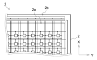
- FIG. 1 is a schematic diagram showing the overall configuration of an embodiment of a display panel.
- 3 is a drawing schematically showing a process of forming a conductive film.
- 3 is a drawing schematically showing a process of forming a conductive film.
- 3 is a drawing schematically showing a process of forming a conductive film.
- 3 is a drawing schematically showing a process of forming a conductive film.
- 3 is a drawing schematically showing a process of forming a conductive film.
- This is an AFM photograph of the surface of the substrate.
- This is an AFM photograph of the surface of the substrate.
- the configuration of the display panel 1 as one embodiment will be explained first, and then the details of one embodiment of the method for manufacturing the conductive film included in the display panel 1 will be explained. Then, we conducted a verification and evaluation experiment to confirm the dispersibility and coating properties of the dispersion liquid and radiation-sensitive resin composition using an example of the method for producing a conductive film.Finally, we will explain the details of the verification and evaluation experiment. be done.
- FIG. 1 is a schematic diagram showing the overall configuration of one embodiment of a display panel 1. As shown in FIG. The display panel 1 has a base material 2, and one surface of the base material 2 is provided with an element region 2a and a peripheral region 2b.
- the base material 2 is formed of a material having translucency, and specifically includes, for example, a glass substrate, a quartz substrate, or an organic resin substrate.
- the material for the organic resin substrate include polyimide.
- the organic resin substrate can have a thickness ranging from several micrometers to several tens of micrometers, making it possible to realize a flexible sheet display.
- the element area 2a is an area where elements for displaying images are formed.
- a lower layer electrode is provided, and an insulating layer is provided on the lower layer electrode.
- An organic resin layer is provided on the insulating layer, and a conductive film is provided on the organic resin layer.
- the material of the organic resin layer is an organic material containing a polymer having hydrocarbon groups.
- the material of the conductive film is CNT.
- As the type of CNT single-walled carbon nanotubes or multi-walled carbon nanotubes having two or more layers can be employed, and single-walled carbon nanotubes are preferable.
- a conductive film made of carbon nanotubes has a transmittance that varies depending on the film thickness, but is a transparent conductive film that is transparent to visible light.
- the material constituting the organic resin layer is an organic resin material containing a polymer having a hydrocarbon group.
- examples of the material constituting the organic resin layer include polyimide resin, polyamide resin, polyether resin, polyester resin, and the like.
- the material constituting the organic resin layer is preferably a material containing an aromatic hydrocarbon, and more preferably a material containing a polycyclic aromatic hydrocarbon.
- the first film which is a coating film for forming the conductive film in this embodiment, is formed by applying a dispersion containing carbon nanotubes and a first polymer that is a dispersant.
- the first polymer is not particularly limited, it is preferable to use a polymer whose main component is a polyamic acid having a structural unit represented by formula (1) in terms of improving the dispersibility of carbon nanotubes. Just to be sure, equation (1) is reproduced.
- R 1 is a tetravalent organic group that constitutes a tetracarboxylic acid
- R 2 is a divalent organic group that constitutes a diamine
- n represents a positive integer.
- tetravalent organic group constituting the tetracarboxylic acid represented by R1 include pyromellitic acid, 2,3,6,7-naphthalenetetracarboxylic acid, and 1,2,5,6-naphthalenetetracarboxylic acid.
- Carboxylic acid 1,4,5,8-naphthalenetetracarboxylic acid, 2,3,6,7-anthracenetetracarboxylic acid, 1,2,5,6-anthracenetetracarboxylic acid, 3,3',4,4 '-Biphenyltetracarboxylic acid, 2,3,3',4-biphenyltetracarboxylic acid, bis(3,4-dicarboxyphenyl) ether, 3,3'4,4'-benzophenonetetracarboxylic acid, bis(3 ,4-dicarboxyphenyl) sulfone, bis(3,4-dicarboxyphenyl)methane, 2,2-bis(3,4-dicarboxyphenyl)propane, 1,1,1,3,3,3-hexane Fluoro-2,2-bis(3,4-dicarboxyphenyl)propane, bis(3,4-dicarboxyphenyl)dimethylsilane, bis(3,4-dica
- divalent organic group constituting the diamine represented by R2 include p-phenylenediamine, m-phenylenediamine, 2,5-diaminotoluene, 2,6-diaminotoluene, 4,4'-diamino Biphenyl, 3,3'-dimethyl-4,4'-diaminobiphenyl, 3,3'-dimethoxy-4,4'-diaminobiphenyl, diaminodiphenylmethane, diaminodiphenyl ether, 2,2'-diaminodiphenylpropane, bis(3 ,5-diethyl-4-aminophenyl)methane, diaminodiphenylsulfone, diaminobenzophenone, diaminonaphthalene, 1,4-bis(4-aminophenoxy)benzene, 1,4-bis(4-aminophenyl)benzene, 9, 10-bis(
- R 1 in the above formula (1) is a cyclobutane ring, and the cyclobutane ring is decomposed by light irradiation or heating, causing a structural change in the polyamic acid, and thereby forming the first polyamic acid. This is preferable in that it becomes easier to remove the combined polyamic acid.
- the above-mentioned dispersion liquid may contain an organic solvent as a dispersion medium, for example.
- the radiation-sensitive resin composition to be applied on the first film to form an insulating layer pattern is a polyamic acid having a structural moiety represented by the above formula (1) contained in the coating liquid for forming the first film. (second polymer). Since polyamic acid exhibits solubility in an alkaline aqueous solution, it can be removed, for example, with an alkaline aqueous solution. That is, an alkaline aqueous solution can be used as a developer.
- the developer is preferably an alkaline aqueous solution, an organic solvent, or a mixture thereof, but solutions other than these may be used as long as the material can remove the first polymer. do not have.
- a combination such as a polymer having a carboxyl group and an aqueous solution of TMAH (tetramethylammonium hydroxide) can be adopted.
- the radiation-sensitive resin composition is a material that is applied onto the first film to form the second film, and a pattern is formed on the conductive film by exposing and developing a part of the second film. It becomes possible to simultaneously remove the first polymer remaining in the first film during this development and the first polymer and second polymer present in the exposed areas of the radiation-sensitive resin composition by one development.
- polyimide is used for forming the insulating layer because it has high insulation properties and excellent resistance to organic solvents and the like.
- polyimide can be used for bank layers formed when partitioning light emitting areas.
- the radiation-sensitive resin composition only needs to contain the polyamic acid represented by formula (1) and have a polyamic acid structure, and some substituents may be different. Furthermore, it may contain an alkali-soluble resin other than polyamic acid.
- alkali-soluble resins include polymers obtained by radical polymerization using an unsaturated compound containing a carboxyl group as an alkali-soluble group as a monomer; other alkali-soluble resins include polysiloxane, cardo resin containing a skeleton, phenol novolak resin, cresol novolak resin, biphenyl resin, bisphenol A type resin, bisphenol F type resin, resin having a dicyclopentanyl skeleton, resin having a trisphenol methane skeleton, bisphenol F type epoxy resin, Multifunctional epoxy resin, flexible epoxy resin, brominated epoxy resin, glycidyl ester type epoxy resin, phenoxy resin, biphenyl type epoxy resin, siloxane resin, polyhydroxystyrene resin, s
- the radiation-sensitive resin composition contains a photoacid generator and functions as a positive radiation-sensitive material.
- a photoacid generator quinonediazide compounds are particularly preferred. Quinonediazide compounds generate carboxylic acids when irradiated with radiation.
- the positive radiation-sensitive resin composition can be given a positive radiation-sensitive property in which the exposed portion is removed in a development step.
- the quinonediazide compound preferably includes a condensate of a compound having a phenolic hydroxyl group and naphthoquinonediazide sulfonic acid halide.
- Examples of the compound having a phenolic hydroxyl group include the compounds shown below.
- compounds having a phenolic hydroxyl group include 4,4'-[1-[4-[1-(4-hydroxyphenyl)-1-methylethyl]phenyl]ethylidene]bisphenol, 1,1,1 -tri(p-hydroxyphenyl)ethane is preferred.
- the naphthoquinonediazide sulfonic acid halide include 1,2-naphthoquinonediazide-4-sulfonic acid chloride and 1,2-naphthoquinonediazide-5-sulfonic acid chloride.
- An ester compound (quinonediazide compound) obtained from 1,2-naphthoquinonediazide-4-sulfonic acid chloride has absorption in the i-line (wavelength 365 nm) region and is therefore suitable for i-line exposure.
- an ester compound (quinonediazide compound) obtained from 1,2-naphthoquinonediazide-5-sulfonic acid chloride has absorption in a wide range of wavelengths and is therefore suitable for exposure over a wide range of wavelengths.
- the quinonediazide compounds include 4,4'-[1-[4-[1-(4-hydroxyphenyl)-1-methylethyl]phenyl]ethylidene]bisphenol and 1,2-naphthoquinonediazide-5-sulfonic acid chloride.
- a condensate of 1,1,1-tri(p-hydroxyphenyl)ethane and 1,2-naphthoquinonediazide-5-sulfonic acid chloride is preferred.
- Quinonediazide compounds can be used alone or in combination of two or more.
- the content of the quinonediazide compound in the radiation-sensitive resin composition is preferably 1 part by mass to 100 parts by mass, more preferably 5 parts by mass to 50 parts by mass, based on 100 parts by mass of polyamic acid.
- the photosensitive resin composition may contain a coloring agent to impart reflective properties or light-blocking properties to the organic EL bank.
- the colorant includes at least one colorant selected from the group consisting of white pigments, black organic colorants, black inorganic colorants, and non-black colorants.
- the colorant is a mixture of two or more inorganic or organic colorants.
- a white pigment When imparting reflectivity to the organic EL bank, a white pigment can be used.
- white pigments include alumina, magnesium oxide, antimony oxide, titanium oxide, zirconium oxide, aluminum hydroxide, magnesium hydroxide, barium sulfate, magnesium carbonate, barium carbonate, calcium carbonate, lead sulfate, lead phosphate, and zinc phosphate. , silicon dioxide, zinc oxide, tin oxide, strontium sulfide, strontium titanate, barium tungstate, lead metasilicate, talc, kaolin, clay, bismuth chloride oxide, hollow silica particles, organic hollow particles, core shell particles, etc. be able to
- the white pigment may contain at least one inorganic substance selected from the group consisting of alumina, magnesium oxide, antimony oxide, titanium oxide, zirconium oxide, aluminum hydroxide, magnesium hydroxide, barium sulfate, magnesium carbonate, and barium carbonate.
- at least one inorganic substance selected from the group consisting of alumina, magnesium oxide, antimony oxide, titanium oxide, zirconium oxide, aluminum hydroxide, magnesium hydroxide, barium sulfate, magnesium carbonate, and barium carbonate.
- titanium oxide is included. Since the above-mentioned inorganic substance has a high refractive index, it is possible to improve the reflection characteristics of the cured film that is formed. Among them, titanium oxide has a particularly high refractive index and is also preferable from the viewpoint of dispersion characteristics in solvents.
- the lower limit of the average particle diameter of the white pigment is preferably 50 nm, preferably 100 nm, and more preferably 200 nm. On the other hand, this upper limit is preferably 700 nm, more preferably 500 nm, and even more preferably 400 nm.
- the average particle diameter of the white pigment is within the above range, good dispersibility, light scattering properties, etc. can be exhibited, and as a result, light reflection properties and light blocking properties can be improved.
- At least one colorant selected from the group consisting of a black organic colorant, a black inorganic colorant, and a colorant other than black can be used.
- any black inorganic colorant, any black organic colorant, and any non-black colorant known in the art may be used.
- any compound classified as a pigment in the Color Index (published by the Society of Dyeing and Color Engineers) and dyes known in the art can be used.
- a specific example of a black organic colorant is at least one selected from the group consisting of aniline black, lactam black, and perylene black.
- lactam black represented by the following formula (for example, Irgaphor Black S 0100 CF manufactured by BASF) in terms of optical density, dielectric constant, transmittance, etc.
- perylene black it is preferable to use perylene black represented by the following formula (manufactured by BASF, LumogenBlack FK42809) in terms of optical density, dielectric constant, transmittance, etc.
- black inorganic colorants include carbon black, titanium black, metal oxides such as Cu-Fe-Mn based oxides, synthetic iron black, and the like. From the viewpoint of pattern characteristics and chemical resistance, it is preferable to use carbon black.
- colorants other than black include C.I. I. Pigment Violet 13, 14, 19, 23, 25, 27, 29, 32, 33, 36, 37 and 38 and C.I. I. Pigment Blue 15 (15:3, 15:4, 15:6 etc.), 16, 21, 28, 60, 64 and 76 may be mentioned.
- the non-black colorant may include at least one colorant selected from the group consisting of a blue colorant and a violet colorant. From the viewpoint of reducing reflectance, C. I. Pigment Blue 15:6 and 60 or C.I. I. Pigment Violet 23.
- the colorant is contained in an amount of 1 to 50% by mass, preferably 5 to 20% by mass, based on the total amount of the photosensitive resin composition.
- the optical density is excellent, and when the colorant is contained in an amount of 5 to 20% by weight, the optical density can be even more excellent.
- the solid content in the photosensitive resin composition means the total of the components from which the solvent is removed.
- the radiation-sensitive resin composition contains a photoacid generator (other than a quinone diazide compound), an antioxidant, a polyfunctional acrylate, a surfactant, an adhesion aid, an inorganic oxide particle, a compound having a cyclic ether group, a solvent, etc. It may also contain other optional ingredients. Other optional components may be used alone or in combination of two or more.
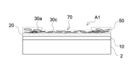
- FIGS. 2 to 6 are drawings schematically showing the process of forming a conductive film. Note that in the method for manufacturing a conductive film of this embodiment, a conductive film is manufactured on an organic resin layer formed on a substrate.
- an organic resin layer 20 is formed on the base material 2 on which the insulating layer 10 is formed by applying an organic resin material containing a polymer having a hydrocarbon group. .
- step S1 On the substrate on which the organic resin layer 20 is formed, as shown in FIG. A pattern is formed (step S1).
- Step S2 Step S1 and step S2 correspond to step (A).
- step S1 a pattern is formed by a coating film of a dispersion containing CNTs on the organic resin layer 20 using a printing technique such as casting, screen printing, or inkjet.
- step S3 corresponds to step (B).
- step S4 corresponds to step (C).
- the radiation-sensitive resin composition forming the second film 50 contains a quinonediazide compound, and therefore functions as a positive-type radiation-sensitive resin material.
- the quinonediazide compound changes to an indenecarboxylic acid structure, so that it becomes soluble in the alkaline aqueous solution.
- the radiation L1 used for exposure is preferably radiation with a wavelength in the range of 190 nm to 450 nm, and more preferably radiation containing ultraviolet rays of 365 nm.
- the exposure amount is preferably 500 J/m 2 to 6,000 J/m 2 , more preferably 1,500 J/m 2 to 1,800 J/m 2 .
- This exposure amount is a value obtained by measuring the intensity of radiation at a wavelength of 365 nm using a luminometer ("OAI model 356" manufactured by OAI Optical Associates).
- a halftone mask can be used as the photomask 60. By using a halftone mask, it is possible to control the shape of the resulting pattern. Specifically, it becomes possible to control the inclination (also referred to as taper shape) of the pattern sidewall.
- step S4 the polyamic acid 30a, which is the second polymer of the radiation-sensitive resin composition layer in the exposed area A1, is developed by using an alkaline aqueous solution as a developer after exposure. It is removed (step S5). This step S5 corresponds to step (D).
- the conductive film 70 is formed in a part of the organic resin layer 20, and a region where the second film 50 remains is formed in the other part. Note that, as shown in FIG. 6, the conductive film 70 has a structure in which CNTs 30c are dispersed and is transparent to visible light, that is, it is transparent.
- the first polymer of the dispersion liquid and the second polymer contained in the radiation-sensitive resin composition are polymers having a polyamic acid structure, and since the polymer having a polyamic acid structure has a carboxyl group in the molecule, High solubility in alkaline aqueous developer.
- alkaline aqueous solution for example, KOH (potassium hydroxide), NaOH (sodium hydroxide), sodium carbonate, TMAH (tetramethylammonium hydroxide) aqueous solution, etc. can be suitably used.
- step S5 the polyamic acid 30a of the first film 40 and the polyamic acid 30a of the second film 50 in the exposed area A1 are removed simultaneously by further development, and the exposed carbon material can be etched. Through this etching process, the film made of carbon material is patterned (step S6). This step S6 corresponds to step (E).
- step S5 the exposed portion A2 of the second film 50 is added to the remaining radiation-sensitive resin composition forming the second film 50 through a photomask, as in step S4.
- step S8 of creating a new exposed portion of the conductive film 70 may be performed by exposing (step S7) and developing with a developer similarly to step S5. Steps S7 and S8 correspond to step (F) and step (G), respectively.
- the conductive film 70 can be precisely patterned using the radiation-sensitive resin composition, and at the same time, the conductive film 70 from which the polyamic acid has been removed and the polyamic acid structure changed to a polyimide structure. It becomes possible to form a pattern with Due to this effect, finer wiring can be formed in, for example, a touch panel or a substrate for a solar cell, which can contribute to more complicated wiring design and higher integration than in the past.
- Examples of methods for applying the dispersion include spray coating, roll coating, spin coating, slit die coating, bar coating, solution dipping, An appropriate method such as an inkjet method can be employed.
- the conductive film is formed with a constant thickness by a predetermined method.
- the methods for applying the radiation-sensitive resin composition are similar, such as spray coating, roll coating, spin coating, slit die coating, and bar coating.
- An appropriate method such as a solution immersion method, an inkjet method, etc. can be employed.
- the conductive film is formed with a constant thickness by a predetermined method.
- the content of the first polymer in the dispersion applied onto the organic resin layer 20 is within the range of 1,000% by mass to 100,000% by mass relative to the CNTs 30a.
- the content of the first polymer to the CNTs 30c within the range, non-uniformity of the solvent in the drying process is prevented, and the CNTs 30c are aggregated and localized on the organic resin layer 20 during drying. Storage is suppressed.
- the slit die coating method or the inkjet method is preferable from the viewpoint of uniformity of the coating film thickness and liquid saving. Further, from the viewpoint that electrode patterning can be performed only by coating, the inkjet method is more preferable.
- the conductive film formed on the organic resin layer exhibits unique electrical properties, has excellent adhesion to the organic resin layer, and has excellent chemical resistance and flatness. will also be good.
- the CNTs 30c included in the first film 40 exhibit high adhesion to the organic resin layer 20, so that the solvent agglomerates in the drying process. Accordingly, the effect of being difficult to localize can be obtained. Furthermore, even in the solution immersion process for removing the first polymer, CNTs do not peel or aggregate, and localization of CNTs is suppressed, resulting in wiring with a very narrow pattern width. Even in this case, it is possible to obtain the effect that locally high resistance parts and disconnections are less likely to occur.
- the method for manufacturing a conductive film includes forming an insulating layer 10 on a base material 2, forming an organic resin layer 20 after forming the insulating layer 10, and forming an organic resin layer 20 on the organic resin layer 20.
- the method may also include forming a conductive film 70 made of CNTs 30a.
- the CNTs 30a contained in the dispersion liquid include at least one of a single-walled nanotube and a multi-walled nanotube. According to such a method of manufacturing a conductive film, it is possible to form a semiconductor device in which the adhesiveness between the organic resin layer 20 and the conductive film 70 is even better. Moreover, the manufacturing yield becomes even better. Furthermore, as a carbon material other than carbon nanotubes, for example, graphene or fullerene, which have excellent conductivity, can be used, but materials other than these may be used as long as they exhibit conductivity.
- the method for manufacturing the conductive film described above can be applied not only to the manufacture of the display panel 1 but also to the manufacture of all electronic devices. Suitable for manufacturing devices, etc.
- the organic resin layer may be formed by the steps shown below.
- the organic resin layer formed by the steps described below exhibits unique electrical properties, has excellent adhesion to CNTs, and has good chemical resistance and flatness. Further, according to the formation method, since heating is performed at 140° C. or lower, thermal deterioration of the substrate and elements provided on the substrate is suppressed. Each step will be explained in detail below.
- Step (1) a coating film is formed on the insulating layer using the radiation-sensitive resin composition. Specifically, a coating film of the radiation-sensitive resin composition is formed by applying the radiation-sensitive resin composition to the surface of the insulating layer. In addition, in order to remove the solvent contained in the coating film, it is preferable that a pre-baking treatment is performed in this step.
- an appropriate method such as a spray method, a roll coating method, a spin coating method, a slit die coating method, a bar coating method, an inkjet method, etc. can be adopted.
- the inkjet method is preferred as the coating method.
- the prebaking conditions may vary depending on the type of each component, the proportion used, etc., but may be, for example, at 60° C. to 130° C. for about 30 seconds to 10 minutes.
- the thickness of the coating film formed after prebaking is preferably 0.1 ⁇ m to 5 ⁇ m, more preferably 0.1 ⁇ m to 1 ⁇ m, and even more preferably 0.2 ⁇ m to 0.4 ⁇ m.
- Step (2) In this step, a portion of the coating film is irradiated (exposed) with radiation. Specifically, the coating film formed in step (1) is irradiated with radiation through a photomask having a predetermined pattern. Depending on the pattern of the photomask used, it is possible to form patterns such as contact hole formation and line and space formation.
- the radiation used at this time examples include ultraviolet rays, deep ultraviolet rays, X-rays, and charged particle beams.
- the photomask used may be a multi-tone photomask such as a halftone mask or a graytone mask.
- Examples of the ultraviolet light include g-line (wavelength: 436 nm), i-line (wavelength: 365 nm), KrF excimer laser light (wavelength: 248 nm), and the like.
- Examples of the X-ray include synchrotron radiation.
- Examples of the charged particle beam include an electron beam. Among these radiations, ultraviolet rays are preferable, and ultraviolet rays with a wavelength of 200 nm or more and 380 nm or less are more preferable.
- the amount of radiation exposure is preferably 1,000 J/m 2 to 20,000 J/m 2 .
- PEB post-exposure bake
- Step (3) the coating film irradiated with radiation is developed.
- the coating film irradiated with radiation in step (2) is developed with a developer to remove the radiation irradiated portion.
- the developer include an alkaline aqueous solution in which potassium hydroxide, sodium carbonate, triethanolamine, tetramethylammonium hydroxide (TMAH), tetraethylammonium hydroxide, etc. are dissolved in water, ethanol, isopropyl alcohol, acetone, ethyl acetate, Organic solvents such as butyl acetate can be used.
- an appropriate method such as a liquid piling method, a dipping method, a rocking immersion method, a shower method, etc. can be adopted, for example.
- the development time varies depending on the composition of the radiation-sensitive resin composition, but can be, for example, 30 seconds to 120 seconds.
- Step (4) the coating film after the above step (3) can be heated.
- the coating film is cured by heat treatment (post-baking) using a heating device such as a hot plate or an oven.
- the upper limit of the heating temperature in this step is 140°C, and the heating temperature may be 130°C, 125°C, or 115°C. According to the formation method, the coating film can be formed into a good shape even by heating at a relatively low temperature.
- BAF 2,2'-bis(3-amino-4-hydroxyphenyl)hexafluoropropane
- BAHF 2,2'-bis(3-amino-4-hydroxyphenyl)hexafluoropropane
- TCA 2,3,5-tricarboxycyclopentyl acetic dianhydride
- TMHQ 1,3-dihydro-1,3-dioxo-5-isobenzofurancarboxylic acid-1,4-phenylene ester
- PAA polyamic acid solution
- a radiation-sensitive resin composition (P-1) was prepared.
- a radiation-sensitive resin composition (P-2) was prepared.
- a quinonediazide compound (4,4'-[1-[4-[1-( 30 parts by mass of a condensate of 4-hydroxyphenyl)-1-methylethyl]phenyl]ethylidene]bisphenol and 1,2-naphthoquinonediazide-5-sulfonic acid chloride), and an adhesion aid (1:3-glycidyloxy 3 parts by mass of propyltrimethoxysilane) were mixed and dissolved in a solvent (propylene glycol monomethyl ether acetate (PGMEA)) so that the solid content concentration was 30% by mass, and then filtered through a membrane filter with a pore size of 0.2 ⁇ m.
- a radiation-sensitive resin composition (pp-1) was prepared.
- the substrates on which the coating films were formed are referred to as (S-1) substrate, (S-2) substrate, and (ss-1) substrate, respectively.
- the obtained pattern shape was evaluated using a SEM (scanning electron microscope). If the cross section of the obtained pattern has a forward taper shape, it is judged as "Good (A)", and if the taper angle is smaller than that of a forward taper and the shape is close to perpendicular to the substrate, it is judged as “Good (B)”, and the space part is judged as “Good (B)”. When there was an undissolved residue on the film and it was recognized that the development was insufficient, it was evaluated as "Poor (C)".
- the film of the light-emitting material whose pattern has a forward tapered cross section is formed smoothly, without any part of the thin film layer becoming thin or interrupted, and with no unevenness in brightness within the light-emitting region. This is preferable in that it can prevent problems such as the following.
- the results are shown in Table 2.
- FIG. 7 and 8 are photographs taken using an AFM (atomic force scanning microscope) of the surface of the space portion of the substrate, and FIG. 7 is an example of a photograph of the substrate surface where the unevenness of CNTs is observed.
- FIG. 8 is an example of a photograph of the substrate surface in which the unevenness of the CNTs is not observed by AFM, that is, the CNTs are covered with the resin/first polymer. If the first polymer on the surface was removed and CNTs (carbon nanotubes) were exposed as shown in FIG. 7, it was evaluated as "good (A)", and as shown in FIG. If the surface was covered with resin and no exposed CNTs were observed, or if the film formation was poor and could not be determined, it was classified as "poor (C)."
- Display panel 2 Base material 10: Insulating layer 20: Organic resin layer 30: Coating film 40: First film 50: Second film 60: Photomask 70: Conductive layer 80: Pattern
Landscapes
- Chemical & Material Sciences (AREA)
- Engineering & Computer Science (AREA)
- Life Sciences & Earth Sciences (AREA)
- Wood Science & Technology (AREA)
- Materials Engineering (AREA)
- Chemical Kinetics & Catalysis (AREA)
- Physics & Mathematics (AREA)
- Organic Chemistry (AREA)
- Optics & Photonics (AREA)
- Plasma & Fusion (AREA)
- General Chemical & Material Sciences (AREA)
- Materials For Photolithography (AREA)
- Electroluminescent Light Sources (AREA)
Priority Applications (3)
| Application Number | Priority Date | Filing Date | Title |
|---|---|---|---|
| CN202380062324.5A CN119816381A (zh) | 2022-09-02 | 2023-08-15 | 导电膜的制造方法、分散液、感放射线性树脂组合物、发光元件 |
| KR1020257006412A KR20250057796A (ko) | 2022-09-02 | 2023-08-15 | 도전막의 제조 방법, 분산액, 감방사선성 수지 조성물, 발광 소자 |
| JP2024544109A JPWO2024048270A1 (https=) | 2022-09-02 | 2023-08-15 |
Applications Claiming Priority (2)
| Application Number | Priority Date | Filing Date | Title |
|---|---|---|---|
| JP2022140054 | 2022-09-02 | ||
| JP2022-140054 | 2022-09-02 |
Publications (1)
| Publication Number | Publication Date |
|---|---|
| WO2024048270A1 true WO2024048270A1 (ja) | 2024-03-07 |
Family
ID=90099305
Family Applications (1)
| Application Number | Title | Priority Date | Filing Date |
|---|---|---|---|
| PCT/JP2023/029520 Ceased WO2024048270A1 (ja) | 2022-09-02 | 2023-08-15 | 導電膜の製造方法、分散液、感放射線性樹脂組成物、発光素子 |
Country Status (5)
| Country | Link |
|---|---|
| JP (1) | JPWO2024048270A1 (https=) |
| KR (1) | KR20250057796A (https=) |
| CN (1) | CN119816381A (https=) |
| TW (1) | TW202412021A (https=) |
| WO (1) | WO2024048270A1 (https=) |
Cited By (1)
| Publication number | Priority date | Publication date | Assignee | Title |
|---|---|---|---|---|
| WO2026004678A1 (ja) * | 2024-06-28 | 2026-01-02 | 日産化学株式会社 | 積層体のパターン形成方法及びそれに用いる組成物 |
Citations (6)
| Publication number | Priority date | Publication date | Assignee | Title |
|---|---|---|---|---|
| JP2000214585A (ja) * | 1999-01-25 | 2000-08-04 | Inst Of Physical & Chemical Res | 感光性樹脂組成物 |
| JP2006281189A (ja) * | 2005-04-04 | 2006-10-19 | Mikuni Denshi Kk | インクジェット塗布溶液と乾燥方法 |
| JP2016087602A (ja) * | 2014-10-31 | 2016-05-23 | Jsr株式会社 | 親液部と撥液部を有する基材の製造方法、組成物、導電膜の形成方法、電子回路および電子デバイス |
| JP2022022537A (ja) * | 2020-06-26 | 2022-02-07 | 東レ株式会社 | 感光性組成物、硬化物および有機el表示装置 |
| WO2022039034A1 (ja) * | 2020-08-18 | 2022-02-24 | 東レ株式会社 | 着色感光性樹脂組成物、硬化物、表示装置及び硬化物の製造方法 |
| WO2022181419A1 (ja) * | 2021-02-26 | 2022-09-01 | 東レ株式会社 | 感光性樹脂組成物、硬化物、表示装置、有機el表示装置および半導体装置 |
Family Cites Families (1)
| Publication number | Priority date | Publication date | Assignee | Title |
|---|---|---|---|---|
| JP5347610B2 (ja) | 2009-03-18 | 2013-11-20 | 東レ株式会社 | 透明導電膜付き基材の製造方法 |
-
2023
- 2023-08-14 TW TW112130484A patent/TW202412021A/zh unknown
- 2023-08-15 WO PCT/JP2023/029520 patent/WO2024048270A1/ja not_active Ceased
- 2023-08-15 CN CN202380062324.5A patent/CN119816381A/zh active Pending
- 2023-08-15 KR KR1020257006412A patent/KR20250057796A/ko active Pending
- 2023-08-15 JP JP2024544109A patent/JPWO2024048270A1/ja active Pending
Patent Citations (6)
| Publication number | Priority date | Publication date | Assignee | Title |
|---|---|---|---|---|
| JP2000214585A (ja) * | 1999-01-25 | 2000-08-04 | Inst Of Physical & Chemical Res | 感光性樹脂組成物 |
| JP2006281189A (ja) * | 2005-04-04 | 2006-10-19 | Mikuni Denshi Kk | インクジェット塗布溶液と乾燥方法 |
| JP2016087602A (ja) * | 2014-10-31 | 2016-05-23 | Jsr株式会社 | 親液部と撥液部を有する基材の製造方法、組成物、導電膜の形成方法、電子回路および電子デバイス |
| JP2022022537A (ja) * | 2020-06-26 | 2022-02-07 | 東レ株式会社 | 感光性組成物、硬化物および有機el表示装置 |
| WO2022039034A1 (ja) * | 2020-08-18 | 2022-02-24 | 東レ株式会社 | 着色感光性樹脂組成物、硬化物、表示装置及び硬化物の製造方法 |
| WO2022181419A1 (ja) * | 2021-02-26 | 2022-09-01 | 東レ株式会社 | 感光性樹脂組成物、硬化物、表示装置、有機el表示装置および半導体装置 |
Cited By (1)
| Publication number | Priority date | Publication date | Assignee | Title |
|---|---|---|---|---|
| WO2026004678A1 (ja) * | 2024-06-28 | 2026-01-02 | 日産化学株式会社 | 積層体のパターン形成方法及びそれに用いる組成物 |
Also Published As
| Publication number | Publication date |
|---|---|
| TW202412021A (zh) | 2024-03-16 |
| CN119816381A (zh) | 2025-04-11 |
| JPWO2024048270A1 (https=) | 2024-03-07 |
| KR20250057796A (ko) | 2025-04-29 |
Similar Documents
| Publication | Publication Date | Title |
|---|---|---|
| KR100743338B1 (ko) | 표시 장치 | |
| WO2019059359A1 (ja) | 着色樹脂組成物、着色膜、カラーフィルターおよび液晶表示装置 | |
| TWI726960B (zh) | 膜觸控感測器及其製作方法 | |
| EP1662322A2 (en) | Positive type photo-sensitive siloxane composition, curing film formed by the composition and device with the curing film | |
| JP2011048195A (ja) | 光学素子隔壁形成用感光性組成物、これを用いたブラックマトリックスおよびその製造方法、並びにカラーフィルタオンアレイの製造方法 | |
| KR20040040349A (ko) | 감광성 수지조성물, 릴리프패턴의 형성방법 및 전자부품 | |
| WO2019182041A1 (ja) | 硬化膜の製造方法、及び有機elディスプレイの製造方法 | |
| WO2024048270A1 (ja) | 導電膜の製造方法、分散液、感放射線性樹脂組成物、発光素子 | |
| JP2009086357A (ja) | 感光性樹脂組成物、該組成物を用いるパターンの製造法および電子デバイス | |
| TW468092B (en) | Radiation-sensitive resin composition for use in spacer, producing method of spacer, spacer and liquid crystal display element | |
| JP2012155226A (ja) | ポジ型感放射線性組成物、硬化膜、硬化膜の形成方法、表示素子、及び硬化膜形成用のポリシロキサン | |
| JP4556639B2 (ja) | ネガ型感光性樹脂組成物、それから形成された透明硬化膜、および硬化膜を有する素子 | |
| JP2008040324A (ja) | 樹脂組成物およびそれを用いたパターン化樹脂膜の製造方法 | |
| JP2024082310A (ja) | 導電膜の製造方法、タッチパネル、ディスプレイパネル | |
| WO2023095785A1 (ja) | 感光性樹脂組成物、硬化物、有機el表示装置、半導体装置および硬化物の製造方法 | |
| WO2023238530A1 (ja) | 導電膜の製造方法、タッチパネル、ディスプレイパネル | |
| JP4878525B2 (ja) | ポジ型感光性樹脂組成物 | |
| JPH11338143A (ja) | ポジ型感光性ポリイミド前駆体樹脂組成物及びこれを用いたレリーフパターンの製造法 | |
| KR101813669B1 (ko) | 신규 가교제 화합물, 이를 포함하는 감광성 폴리이미드 조성물 및 이의 제조방법 | |
| WO2025057653A1 (ja) | 導電膜の製造方法、タッチパネル、ディスプレイパネル | |
| WO2023238765A1 (en) | Method for producing vertical organic light-emitting transistor device, display | |
| JP2004035685A (ja) | アルカリ可溶性樹脂 | |
| JP2010243748A (ja) | 感光性樹脂組成物および耐熱性樹脂膜の製造方法 | |
| KR101421789B1 (ko) | 패턴의 제조방법 | |
| EP4737506A1 (en) | Cured film and organic el display device |
Legal Events
| Date | Code | Title | Description |
|---|---|---|---|
| 121 | Ep: the epo has been informed by wipo that ep was designated in this application |
Ref document number: 23860035 Country of ref document: EP Kind code of ref document: A1 |
|
| WWE | Wipo information: entry into national phase |
Ref document number: 2024544109 Country of ref document: JP |
|
| WWE | Wipo information: entry into national phase |
Ref document number: 202380062324.5 Country of ref document: CN |
|
| NENP | Non-entry into the national phase |
Ref country code: DE |
|
| WWP | Wipo information: published in national office |
Ref document number: 202380062324.5 Country of ref document: CN |
|
| WWP | Wipo information: published in national office |
Ref document number: 1020257006412 Country of ref document: KR |
|
| 122 | Ep: pct application non-entry in european phase |
Ref document number: 23860035 Country of ref document: EP Kind code of ref document: A1 |