WO2024038657A1 - 積層セラミックコンデンサ - Google Patents
積層セラミックコンデンサ Download PDFInfo
- Publication number
- WO2024038657A1 WO2024038657A1 PCT/JP2023/020657 JP2023020657W WO2024038657A1 WO 2024038657 A1 WO2024038657 A1 WO 2024038657A1 JP 2023020657 W JP2023020657 W JP 2023020657W WO 2024038657 A1 WO2024038657 A1 WO 2024038657A1
- Authority
- WO
- WIPO (PCT)
- Prior art keywords
- ceramic capacitor
- multilayer ceramic
- layer
- drawer
- height direction
- Prior art date
- Legal status (The legal status is an assumption and is not a legal conclusion. Google has not performed a legal analysis and makes no representation as to the accuracy of the status listed.)
- Ceased
Links
Images


Classifications
-
- H—ELECTRICITY
- H01—ELECTRIC ELEMENTS
- H01G—CAPACITORS; CAPACITORS, RECTIFIERS, DETECTORS, SWITCHING DEVICES, LIGHT-SENSITIVE OR TEMPERATURE-SENSITIVE DEVICES OF THE ELECTROLYTIC TYPE
- H01G4/00—Fixed capacitors; Processes of their manufacture
- H01G4/30—Stacked capacitors
-
- H—ELECTRICITY
- H01—ELECTRIC ELEMENTS
- H01G—CAPACITORS; CAPACITORS, RECTIFIERS, DETECTORS, SWITCHING DEVICES, LIGHT-SENSITIVE OR TEMPERATURE-SENSITIVE DEVICES OF THE ELECTROLYTIC TYPE
- H01G4/00—Fixed capacitors; Processes of their manufacture
- H01G4/002—Details
- H01G4/005—Electrodes
- H01G4/012—Form of non-self-supporting electrodes
-
- H—ELECTRICITY
- H01—ELECTRIC ELEMENTS
- H01G—CAPACITORS; CAPACITORS, RECTIFIERS, DETECTORS, SWITCHING DEVICES, LIGHT-SENSITIVE OR TEMPERATURE-SENSITIVE DEVICES OF THE ELECTROLYTIC TYPE
- H01G4/00—Fixed capacitors; Processes of their manufacture
- H01G4/002—Details
- H01G4/018—Dielectrics
- H01G4/06—Solid dielectrics
- H01G4/08—Inorganic dielectrics
- H01G4/12—Ceramic dielectrics
- H01G4/1209—Ceramic dielectrics characterised by the ceramic dielectric material
- H01G4/1218—Ceramic dielectrics characterised by the ceramic dielectric material based on titanium oxides or titanates
- H01G4/1227—Ceramic dielectrics characterised by the ceramic dielectric material based on titanium oxides or titanates based on alkaline earth titanates
-
- H—ELECTRICITY
- H01—ELECTRIC ELEMENTS
- H01G—CAPACITORS; CAPACITORS, RECTIFIERS, DETECTORS, SWITCHING DEVICES, LIGHT-SENSITIVE OR TEMPERATURE-SENSITIVE DEVICES OF THE ELECTROLYTIC TYPE
- H01G4/00—Fixed capacitors; Processes of their manufacture
- H01G4/002—Details
- H01G4/224—Housing; Encapsulation
-
- H—ELECTRICITY
- H01—ELECTRIC ELEMENTS
- H01G—CAPACITORS; CAPACITORS, RECTIFIERS, DETECTORS, SWITCHING DEVICES, LIGHT-SENSITIVE OR TEMPERATURE-SENSITIVE DEVICES OF THE ELECTROLYTIC TYPE
- H01G4/00—Fixed capacitors; Processes of their manufacture
- H01G4/002—Details
- H01G4/228—Terminals
- H01G4/232—Terminals electrically connecting two or more layers of a stacked or rolled capacitor
Definitions
- the present invention relates to a multilayer ceramic capacitor.
- a typical multilayer ceramic capacitor has a generally rectangular parallelepiped-shaped laminate whose dimension in the length direction L is longer than the dimension in the width direction W, and external electrodes are provided at both ends of the laminate in the length direction L. It is being On the other hand, so-called LW inversion type multilayer ceramic capacitors are also known, in which the size relationship between the length direction L dimension and the width direction W dimension of the laminate is reversed in order to reduce ESL (Patent Document 1 and (See Patent Document 2).
- Patent Document 2 discloses that an edge of at least one of the fourth and fifth surfaces of an external electrode is provided with a recess that is recessed from the edge toward the first surface, and both sides of the recess in the third direction
- An LW inversion type multilayer ceramic electronic component is disclosed in which the portion is a covering portion that covers the ridges of two surfaces in the second direction of the component body.
- the laminated ceramic electronic component is likely to rotate or tilt, and there is a possibility that the mounting performance may be deteriorated.
- the distance between the lands of the board on which the LW reversal type multilayer ceramic electronic component is mounted is short, the self-alignment effect deteriorates, and if the multilayer ceramic electronic component rotates significantly, the polarity may change. If one external electrode is mounted so as to straddle different lands, a short-circuit failure may occur.
- An object of the present invention is to provide an LW inversion type multilayer ceramic capacitor that can suppress deterioration of the self-alignment effect and perform stable mounting.
- the multilayer ceramic capacitor according to the present invention includes a plurality of dielectric layers and a plurality of internal electrode layers alternately stacked in the height direction, and a first main surface and a second main surface facing each other in the height direction. a first end face and a second end face facing each other in a length direction perpendicular to the height direction, and a first side face and a second end face facing each other in a width direction perpendicular to the height direction and the length direction. 2 side surfaces, a first surface portion located on the first end surface, a second surface portion located on a part of the first main surface, and a second surface portion located on the second main surface.
- a first external electrode having a sixth surface portion located on the second end surface, a seventh surface portion located on a portion of the first main surface, and a seventh surface portion located on a portion of the second main surface.
- a second surface having at least one of the eighth surface portions located on the second side surface, a ninth surface portion located on a portion of the first side surface, and a tenth surface portion located on a portion of the second side surface.
- the length in the longitudinal direction connecting the first end face and the second end face of the multilayer body is l
- the first side surface and the second end face are
- w is the length in the width direction connecting the side surfaces of
- t is the length in the height direction connecting the first main surface and the second main surface, the dimensional relationship w>l>t.
- the fourth surface, the fifth surface, the ninth surface, and the tenth surface have openings through which the surface of the laminate is exposed;
- the fifth surface portion and the tenth surface portion each have a convex portion that protrudes in the longitudinal direction from the longitudinal center side facing each other.
- an LW inversion type multilayer ceramic capacitor that can suppress deterioration of the self-alignment effect and perform stable mounting.
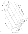
- FIG. 1 is an external perspective view of a multilayer ceramic capacitor according to an embodiment.
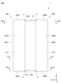
- FIG. 2 is a view in the direction of arrows when the multilayer ceramic capacitor shown in FIG. 1 is viewed from a first side surface side along the direction of arrow II.
- FIG. 2 is a view in the direction of arrows when the multilayer ceramic capacitor shown in FIG. 1 is viewed from a second side surface side along the direction of arrow III.
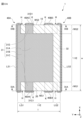
- FIG. 3 is a view in the direction of arrows when the multilayer ceramic capacitor shown in FIG. 2 is viewed from the first main surface side along the direction of arrow IV.
- FIG. 3 is a view in the direction of arrows when the multilayer ceramic capacitor shown in FIG. 2 is viewed from the second main surface side along the direction of arrow V.
- FIG. 2 is a view in the direction of arrows when the multilayer ceramic capacitor shown in FIG. 1 is viewed from a first side surface side along the direction of arrow II.
- FIG. 2 is a view in the
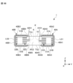
- FIG. 5 is a cross-sectional view of the multilayer ceramic capacitor shown in FIG. 4 taken along line VI-VI.
- 7 is a sectional view taken along line VII-VII of the multilayer ceramic capacitor shown in FIG. 6.
- FIG. 7 is a sectional view taken along line VIIIA-VIIIA of the multilayer ceramic capacitor shown in FIG. 6, and shows a first internal electrode layer.
- FIG. 7 is a sectional view taken along line VIIIB-VIIIB of the multilayer ceramic capacitor shown in FIG. 6, and is a diagram showing a second internal electrode layer.
- FIG. 5 is a sectional view taken along line IXA-IXA of the multilayer ceramic capacitor shown in FIG. 4, and is a view showing the first side surface of the multilayer body.
- FIG. 5 is a sectional view taken along line IXB-IXB of the multilayer ceramic capacitor shown in FIG. 4, and is a view showing a second side surface of the multilayer body.
- FIG. FIG. 7 is an enlarged view of section XA in FIG. 6, showing a cross section of the first external electrode.
- FIG. 7 is an enlarged view of section XB in FIG. 6, showing a cross section of the second external electrode.
- 10A is a cross-sectional view showing a modification of the layer structure of the external electrode of the multilayer ceramic capacitor of the above embodiment, and is a diagram corresponding to FIG. 10A.
- FIG. 10A is a cross-sectional view showing a modification of the layer structure of the external electrode of the multilayer ceramic capacitor of the above embodiment, and is a diagram corresponding to FIG. 10A.
- FIG. 10B is a cross-sectional view showing a modification of the layer structure of the external electrode of the multilayer ceramic capacitor of the above embodiment, and is a diagram corresponding to FIG. 10B.
- FIG. FIG. 6 is a diagram showing an intermediate state in the manufacturing process of the multilayer ceramic capacitor of the embodiment.
- FIG. 6 is a diagram showing an intermediate state in the manufacturing process of the multilayer ceramic capacitor of the embodiment.
- FIG. 6 is a diagram showing an intermediate state in the manufacturing process of the multilayer ceramic capacitor of the embodiment.
- FIG. 2 is a sectional view showing a modification of the arrangement position of the external electrodes of the multilayer ceramic capacitor of the above embodiment, and corresponds to FIG. 1 .
- 2 is an external perspective view of a multilayer ceramic capacitor of Comparative Example 1, corresponding to FIG. 1.
- FIG. 8A is a diagram showing the first internal electrode layer of the multilayer ceramic capacitor of the comparative example, and corresponds to FIG. 8A.
- 8B is a diagram showing a second internal electrode layer of the multilayer ceramic capacitor of the comparative example, and corresponds to FIG. 8B.
- FIG. 2 is an external perspective view of a multilayer ceramic capacitor of Comparative Example 2, corresponding to FIG. 1.
- FIG. FIG. 8A is a diagram showing the first internal electrode layer of the multilayer ceramic capacitor of the comparative example, and corresponds to FIG. 8A.
- 8B is a diagram showing a second internal electrode layer of the multilayer ceramic capacitor of the comparative example, and corresponds to FIG. 8B.
- FIG. FIG. 3 is a diagram for explaining a method for evaluating mountability in an experimental example.
- FIG. 3 is a diagram for explaining a method for evaluating mountability in an experimental example.
- FIG. 3 is a diagram for explaining a method for evaluating mountability in an experimental example.
- FIG. 3 is a diagram for explaining a method for evaluating mountability in an experimental example.
- FIG. 3 is a diagram for explaining a method for evaluating mountability in an experimental example.
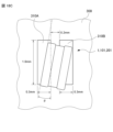
- FIG. 1 is an external perspective view of a multilayer ceramic capacitor 1 according to this embodiment.
- FIG. 2 is a view in the direction of arrows when the multilayer ceramic capacitor 1 shown in FIG. 1 is viewed from the first side surface WS1 along the direction of arrow II.
- FIG. 3 is an arrow view of the multilayer ceramic capacitor 1 shown in FIG. 1 when looking at the second side surface WS2 along the direction of arrow III.
- FIG. 4 is a view in the direction of arrows when the multilayer ceramic capacitor 1 shown in FIG. 2 is viewed from the first main surface TS1 side along the direction of arrow IV.
- FIG. 5 is an arrow view of the multilayer ceramic capacitor 1 shown in FIG.
- FIG. 6 is a cross-sectional view of the multilayer ceramic capacitor 1 shown in FIG. 4 taken along the line VI-VI.
- FIG. 7 is a cross-sectional view of the multilayer ceramic capacitor 1 shown in FIG. 6 taken along line VII-VII.
- FIG. 8A is a cross-sectional view of the multilayer ceramic capacitor 1 shown in FIG. 6 taken along the line VIIIA-VIIIA.
- FIG. 8B is a cross-sectional view of the multilayer ceramic capacitor 1 shown in FIG. 6 taken along the line VIIIB-VIIIB.
- 9A is a cross-sectional view of the multilayer ceramic capacitor 1 shown in FIG.
- FIG. 10A is an enlarged view of the XA section in FIG. 6, and is a diagram showing a cross section of the first external electrode 40A.
- FIG. 10B is an enlarged view of the XB section in FIG. 6, and is a diagram showing a cross section of the second external electrode 40B.
- the multilayer ceramic capacitor 1 includes a multilayer body 10 and an external electrode 40.
- FIGS. 1 to 9B An XYZ orthogonal coordinate system is shown in FIGS. 1 to 9B.
- the length direction L of the multilayer ceramic capacitor 1 and the multilayer body 10 corresponds to the Y direction.
- the width direction W of the multilayer ceramic capacitor 1 and the multilayer body 10 corresponds to the X direction.
- the height direction T of the multilayer ceramic capacitor 1 and the multilayer body 10 corresponds to the Z direction.
- the cross section shown in FIG. 6 is also referred to as the LT cross section.
- the cross section shown in FIG. 7 is also referred to as a WT cross section.
- the cross sections shown in FIGS. 8A and 8B are also referred to as LW cross sections.
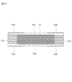
- the laminate 10 has a first main surface TS1 and a second main surface TS2 facing in the height direction T and facing in the length direction L perpendicular to the height direction T. It includes a first end surface LS1 and a second end surface LS2, and a first side surface WS1 and a second side surface WS2 facing in the width direction W perpendicular to the height direction T and the length direction L.
- the laminate 10 has a substantially rectangular parallelepiped shape. It is preferable that the corners and ridges of the laminate 10 be rounded. A corner is a part where three sides of the laminate intersect, and a ridgeline is a part where two sides of the laminate intersect. Incidentally, unevenness may be formed on a part or all of the surface constituting the laminate 10.
- the laminate 10 includes an inner layer portion 11, a first main surface side outer layer portion 12, and a second main surface, which are arranged to sandwich the inner layer portion 11 in the height direction T. It has a side outer layer part 13.
- the inner layer section 11 includes a plurality of dielectric layers 20 and a plurality of internal electrode layers 30.
- the inner layer portion 11 includes, in the height direction T, an internal electrode layer 30 located closest to the first main surface TS1 to an internal electrode layer 30 located closest to the second main surface TS2.
- a plurality of internal electrode layers 30 are arranged facing each other with the dielectric layer 20 interposed therebetween.
- the inner layer portion 11 is a portion that generates capacitance and essentially functions as a capacitor. Note that the inner layer portion 11 is also referred to as an effective layer portion.
- the plurality of dielectric layers 20 are made of dielectric material.
- the dielectric material is, for example, a ceramic material.
- the dielectric material may be, for example, a dielectric ceramic containing components such as BaTiO 3 , CaTiO 3 , SrTiO 3 or CaZrO 3 .
- these components are the main components, depending on the desired properties of the laminate, subcomponents whose content is smaller than the main components, such as Mn compounds, Fe compounds, Cr compounds, Co compounds, Ni compounds, etc. may be added.
- the thickness of the dielectric layer 20 is preferably 0.5 ⁇ m or more and 10 ⁇ m or less.
- the number of dielectric layers 20 to be laminated is preferably 15 or more and 700 or less. Note that the number of dielectric layers 20 is the total number of dielectric layers in the inner layer section 11 and the number of dielectric layers in the first main surface side outer layer section 12 and the second main surface side outer layer section 13. be.
- the plurality of internal electrode layers 30 have a plurality of first internal electrode layers 31 and a plurality of second internal electrode layers 32.
- the first internal electrode layer 31 is arranged on the plurality of dielectric layers 20 and drawn out to the first end surface LS1.
- the second internal electrode layer 32 is arranged on the plurality of dielectric layers 20 and drawn out to the second end surface LS2.
- the plurality of first internal electrode layers 31 and the plurality of second internal electrode layers 32 are alternately arranged in the height direction T of the stacked body 10 with the dielectric layers 20 interposed therebetween.
- the first internal electrode layer 31 and the second internal electrode layer 32 are arranged with the dielectric layer 20 sandwiched therebetween.
- the first internal electrode layer 31 includes a first opposing electrode section 31A that faces the second internal electrode layer 32, and a first end surface LS1, a first opposing electrode section 31A, and a first end surface LS1.
- a first lead-out portion 31B drawn out to a part of the first side surface WS1 and a part of the second side surface WS2, and a second lead-out part 31B drawn out from the first counter electrode part 31A to a part of the first side surface WS1. It has a lead-out part 31C and a third lead-out part 31D drawn out from the first counter electrode part 31A to a part of the second side surface WS2.
- the first counter electrode section 31A is located inside the stacked body 10.
- the first lead-out portion 31B is connected to the first counter electrode portion 31A, and is exposed on the first end surface LS1, a portion of the first side surface WS1, and a portion of the second side surface WS2.
- the second lead-out portion 31C is connected to the first counter electrode portion 31A and is exposed on a part of the first side surface WS1.
- the third lead-out portion 31D is connected to the first counter electrode portion 31A and is exposed on a part of the second side surface WS2.
- the second drawer portion 31C is spaced apart in the length direction L from the portion of the first drawer portion 31B that is drawn out to the first side surface WS1.
- the third drawer portion 31D is spaced apart from the portion of the first drawer portion 31B that is drawn out to the second side surface WS2 in the length direction L.
- the second internal electrode layer 32 includes a second opposing electrode section 32A that faces the first internal electrode layer 31, and a second end surface LS2, a second end surface LS2, a second opposing electrode section 32A, and a A fourth lead-out portion 32B that is drawn out to a part of the first side surface WS1 and a part of the second side surface WS2, and a fifth lead-out part 32B that is drawn out from the second counter electrode part 32A to a part of the first side surface WS1. It has a drawn-out portion 32C and a sixth drawn-out portion 32D drawn out from the second counter electrode portion 32A to a part of the second side surface WS2.
- the second counter electrode section 32A is located inside the stacked body 10.
- the fourth lead-out portion 32B is connected to the second counter electrode portion 32A, and is exposed on the second end surface LS2, a portion of the first side surface WS1, and a portion of the second side surface WS2.
- the fifth lead-out portion 32C is connected to the second counter electrode portion 32A and is exposed on a part of the first side surface WS1.
- the sixth lead-out portion 32D is connected to the second counter electrode portion 32A and is exposed on a part of the second side surface WS2.
- the fifth drawer portion 32C is spaced apart in the length direction L from the portion of the fourth drawer portion 32B that is drawn out to the first side surface WS1.
- the sixth drawer portion 32D is spaced apart from the portion of the fourth drawer portion 32B that is drawn out to the second side surface WS2 in the length direction L.
- FIG. 9A is a cross-sectional view of the multilayer ceramic capacitor 1 shown in FIG. 4 taken along the line IXA-IXA, and is a view showing the first side surface WS1 of the multilayer body 10.
- 9B is a cross-sectional view of the multilayer ceramic capacitor 1 shown in FIG. 4 taken along the line IXB-IXB, and is a view showing the second side surface WS2 of the multilayer body 10.
- the first side surface WS1 of the stacked body 10 includes a first lead-out portion 31B and a second lead-out portion 31C of each of the plurality of first internal electrode layers 31, and a plurality of second The fourth lead-out portion 32B and the fifth lead-out portion 32C of each internal electrode layer 32 are exposed.
- the plurality of first drawer portions 31B and the plurality of second drawer portions 31C are exposed on the surface of the laminate 10 while being separated from each other.
- the plurality of fourth drawer sections 32B and the plurality of fifth drawer sections 32C are exposed on the surface of the laminate 10 in a spaced-apart manner.
- the plurality of second drawer portions 31C located at the center in the height direction T
- the dimension in the length direction L of the drawer portion 31C is such that it is located at a position other than the center part in the height direction T, that is, the first main surface TS1 side and the second main surface TS2 side from the center part in the height direction T. It is longer than the dimension in the length direction L of the second drawer portion 31C located at each of the second drawer portions 31C.
- the positions of the outer ends in the length direction L, that is, the ends on the first end surface LS1 side, of all the second drawer parts 31C are aligned in the length direction L.
- the center side in the length direction L of the plurality of second drawer parts 31C located at the center part in the height direction T is smaller than the plurality of second drawer parts 31C located at the center part in the height direction T. It protrudes toward the center in the length direction L.
- each of the plurality of second drawer parts 31C located at the center part in the height direction T is located at the end of the plurality of second drawer parts 31C on the longitudinal center side other than the center part in the height direction T. It has a protruding portion 31C1 that protrudes from the portion toward the center in the length direction.
- the tip of the protruding portion 31C1 on the center side in the length direction is located closer to the center in the length direction than the end portion 40A9 on the center side in the length direction of the second surface portion 40A2 and the third surface portion 40A3. That is, the longitudinal center side of the plurality of second drawer portions 31C located at the center in the height direction T is longer than the end portion 40A9 of the second surface portion 40A2 and the third surface portion 40A3 on the longitudinal direction center side. It protrudes toward the center in the horizontal direction.
- the dimension in the length direction L of the plurality of fifth drawer portions 32C located at the center in the height direction T is as follows: Length of the fifth drawer portion 32C located outside the center in the height direction T, that is, located closer to the first main surface TS1 and the second main surface TS2 than the center in the height direction T It is longer than the dimension in direction L.
- the positions of the outer ends in the length direction L, that is, the ends on the second end surface LS2 side, of all the fifth drawer parts 32C are aligned in the length direction L.
- the center side in the length direction L of the plurality of fifth drawer parts 32C located at the center part in the height direction T is smaller than the plurality of fifth drawer parts 32C located at the center part in the height direction T. It protrudes toward the center in the length direction L.
- each of the plurality of fifth drawer parts 32C located at the center part in the height direction T is located at the end of the plurality of fifth drawer parts 32C on the longitudinal center side other than the center part in the height direction T. It has a protruding portion 32C1 that protrudes from the portion toward the center in the length direction.
- the tip of the protruding portion 32C1 on the center side in the length direction is located closer to the center in the length direction than the end portion 40B9 on the center side in the length direction of the seventh surface portion 40B2 and the eighth surface portion 40B3. That is, the lengthwise center side of the plurality of fifth drawer portions 32C located at the center in the height direction T is longer than the lengthwise center side end portion 40B9 of the seventh surface portion 40B2 and the eighth surface portion 40B3. It protrudes toward the center in the horizontal direction.
- a plurality of third drawer parts 31D located at the center in the height direction T is the dimension in the length direction L of the drawer portion 31D located at a position other than the center part in the height direction T, that is, the first main surface TS1 side and the second main surface TS2 from the center part in the height direction T. It is longer than the dimension in the length direction L of the third drawer portion 31D located on each side.
- each of the plurality of third drawer parts 31D located at the center part in the height direction T is located at the end of the plurality of third drawer parts 31D other than the center part in the height direction T on the longitudinal center side. It has a protrusion 31D1 that protrudes from the portion toward the center in the length direction.
- the tip of the protruding portion 31D1 on the center side in the length direction is located closer to the center in the length direction than the end portion 40A9 on the center side in the length direction of the second surface portion 40A2 and the third surface portion 40A3. That is, the lengthwise center side of the plurality of third drawer portions 31D located at the center in the height direction T is longer than the end portion 40A9 of the second surface portion 40A2 and the third surface portion 40A3 on the lengthwise center side. It protrudes toward the center in the horizontal direction.
- the dimension in the length direction L of the plurality of sixth drawer portions 32D located at the center in the height direction T is as follows: Length of the sixth drawer portion 32D located outside the center in the height direction T, that is, located closer to the first main surface TS1 and the second main surface TS2 than the center in the height direction T It is longer than the dimension in direction L.
- the positions of the outer ends of all the sixth drawer parts 32D in the length direction L, that is, the ends on the second end surface LS2 side, are aligned in the length direction T.
- the center side in the length direction L of the plurality of sixth drawer parts 32D located at the center part in the height direction T is smaller than the plurality of sixth drawer parts 32D located at the center part in the height direction T. It protrudes toward the center in the length direction L.
- each of the plurality of sixth drawer parts 32D located at the center part in the height direction T is located at the end of the plurality of sixth drawer parts 32D on the longitudinal center side other than the center part in the height direction T. It has a protrusion 32D1 that protrudes from the portion toward the center in the length direction.
- the tip of the protruding portion 32D1 on the center side in the longitudinal direction is located closer to the center in the longitudinal direction than the end portion 40B9 on the center side in the longitudinal direction of the seventh surface portion 40B2 and the eighth surface portion 40B3. That is, the longitudinal center side of the plurality of sixth drawer portions 32D located at the center in the height direction T is longer than the end portion 40B9 of the seventh surface portion 40B2 and the eighth surface portion 40B3 on the longitudinal direction center side. It protrudes toward the center in the horizontal direction.
- the dimensions in the length direction L of the portions of the first drawer portion 31B and the fourth drawer portion 32B that are exposed on a part of the first side surface WS1 are respectively 30 ⁇ m or more and 230 ⁇ m or less. It is preferable that the dimensions in the length direction L of the portions of the first drawer portion 31B and the fourth drawer portion 32B that are exposed on a part of the second side surface WS2 are each 30 ⁇ m or more and 230 ⁇ m or less. It is preferable that the dimensions in the length direction L of the portions of the second drawer portion 31C and the fifth drawer portion 32C that are exposed on a part of the first side surface WS1 are each 30 ⁇ m or more and 230 ⁇ m or less. It is preferable that the dimensions in the length direction L of the portions of the third drawer portion 31D and the sixth drawer portion 32D that are exposed on a part of the second side surface WS2 are each 30 ⁇ m or more and 230 ⁇ m or less.
- each drawer portion exposed on the side surface of these laminates 10 are not particularly limited. However, the dimensions in the length direction L of the portions of the second drawer portion 31C and the fifth drawer portion 32C that are exposed on a part of the first side surface WS1 are the same as those of the first drawer portion 31B and the fourth drawer portion 32B. It may be longer than the dimension in the length direction L of the part exposed to a part of the first side surface WS1.
- the dimensions in the length direction L of the portions of the third drawer portion 31D and the sixth drawer portion 32D that are exposed on a part of the second side surface WS2 are as follows: It may be longer than the dimension in the length direction L of the portion exposed to a part of the side surface WS2 of No. 2.
- the shape of the external electrode 40 of this embodiment having an opening H and a convex part K, which will be described later, can be realized. Since the distance between the second lead-out part 31C of the first internal electrode layer 31 and the fifth lead-out part 32C of the second internal electrode layer 32 can be shortened, the first internal electrode Since the distance between the third lead-out portion 31D of the layer 31 and the sixth lead-out portion 32D of the second internal electrode layer 32 can be shortened, the path through which the current flows can be shortened. Therefore, ESL can be reduced.
- a capacitance is formed by the first counter electrode section 31A and the second counter electrode section 32A facing each other with the dielectric layer 20 in between, and the characteristics of a capacitor are exhibited.
- the shapes of the first counter electrode section 31A and the second counter electrode section 32A are not particularly limited, but are preferably rectangular. However, the rectangular corner portions may be rounded, or the rectangular corner portions may be formed obliquely.
- the shapes of the first drawer part 31B and the fourth drawer part 32B are not particularly limited, but are preferably rectangular. However, the rectangular corner portions may be rounded, or the rectangular corner portions may be formed obliquely. In this embodiment, the shapes of the first drawer part 31B and the fourth drawer part 32B are substantially T-shaped with a part of the rectangular corner part removed.
- the shapes of the second drawer part 31C, the third drawer part 31D, the fifth drawer part 32C, and the sixth drawer part 32D are not particularly limited, but are preferably rectangular.
- the rectangular corner portions may be rounded, or the rectangular corner portions may be formed obliquely.
- the dimension in the width direction W of the portion of the first lead-out portion 31B exposed to the first end surface LS1 is larger than the dimension in the width direction of the first counter electrode portion 31A.
- the dimension in the width direction W of the portion of the fourth lead-out portion 32B exposed to the second end surface LS2 is larger than the dimension in the width direction of the second opposing electrode portion 32A.
- the first internal electrode layer 31 and the second internal electrode layer 32 are made of an appropriate conductive material such as a metal such as Ni, Cu, Ag, Pd, or Au, or an alloy containing at least one of these metals. be done. When using an alloy, the first internal electrode layer 31 and the second internal electrode layer 32 may be made of, for example, an Ag--Pd alloy.
- each of the first internal electrode layer 31 and the second internal electrode layer 32 is preferably about 0.2 ⁇ m or more and 2.0 ⁇ m or less, for example.
- the total number of first internal electrode layers 31 and second internal electrode layers 32 is preferably 15 or more and 200 or less.
- the first main surface side outer layer portion 12 is located on the first main surface TS1 side of the laminate 10.
- the first main surface side outer layer portion 12 is an aggregate of a plurality of dielectric layers 20 located between the first main surface TS1 and the internal electrode layer 30 closest to the first main surface TS1. That is, the first main surface side outer layer portion 12 is located between the first main surface TS1 and the internal electrode layer 30 located closest to the first main surface TS1 among the plurality of internal electrode layers 30. It is formed from a plurality of dielectric layers 20.
- the dielectric layer 20 used in the first main surface side outer layer section 12 may be the same as the dielectric layer 20 used in the inner layer section 11.
- the second main surface side outer layer portion 13 is located on the second main surface TS2 side of the laminate 10.
- the second main surface side outer layer portion 13 is an aggregate of a plurality of dielectric layers 20 located between the second main surface TS2 and the internal electrode layer 30 closest to the second main surface TS2. That is, the second main surface side outer layer portion 13 is located between the second main surface TS2 and the internal electrode layer 30 located closest to the second main surface TS2 among the plurality of internal electrode layers 30. It is formed from a plurality of dielectric layers 20.
- the dielectric layer 20 used in the second main surface side outer layer portion 13 may be the same as the dielectric layer 20 used in the inner layer portion 11.
- the laminate 10 includes a plurality of stacked dielectric layers 20 and a plurality of internal electrode layers 30 stacked on the dielectric layers 20. That is, the multilayer ceramic capacitor 1 has a multilayer body 10 in which dielectric layers 20 and internal electrode layers 30 are alternately stacked.
- the laminate 10 has a counter electrode portion 11E.
- the counter electrode portion 11E is a portion where the first counter electrode portion 31A of the first internal electrode layer 31 and the second counter electrode portion 32A of the second internal electrode layer 32 face each other.
- the counter electrode section 11E is configured as a part of the inner layer section 11. 8A and 8B show the range in the width direction W and length direction L of the counter electrode portion 11E. Note that the counter electrode portion 11E is also referred to as a capacitor effective portion.
- the laminate 10 has an outer layer portion on the end surface side.
- the end surface side outer layer portion includes a first end surface side outer layer portion LG1 located on the first end surface LS1 side and a second end surface side outer layer portion LG2 located on the second end surface LS2 side.
- the first end surface side outer layer portion LG1 is a portion including the dielectric layer 20 and the first extension portion 31B located between the counter electrode portion 11E and the first end surface LS1. That is, the first end surface side outer layer portion LG1 is an assembly of the portions of the plurality of dielectric layers 20 on the first end surface LS1 side and the plurality of first lead-out portions 31B.
- the second end surface side outer layer portion LG2 is a portion including the dielectric layer 20 and the fourth extension portion 32B located between the counter electrode portion 11E and the second end surface LS2. That is, the second end surface side outer layer portion LG2 is an assembly of the portions of the plurality of dielectric layers 20 on the second end surface LS2 side and the plurality of fourth lead-out portions 32B.
- FIG. 8A, and FIG. 8B show the range in the length direction L of the first end surface side outer layer portion LG1 and the second end surface side outer layer portion LG2. Note that the first end surface side outer layer portion LG1 and the second end surface side outer layer portion LG2 are also referred to as an L gap or an end gap.
- the laminate 10 has a side surface side outer layer portion.
- the side surface side outer layer portion includes a first side surface side outer layer portion WG1 located on the first side surface WS1 side and a second side surface side outer layer portion WG2 located on the second side surface WS2 side.
- the first side surface side outer layer portion WG1 is a portion including the dielectric layer 20 located between the counter electrode portion 11E and the first side surface WS1. That is, the first side surface side outer layer portion WG1 is a collection of portions of the plurality of dielectric layers 20 on the first side surface WS1 side.
- the second side surface side outer layer portion WG2 is a portion including the dielectric layer 20 located between the counter electrode portion 11E and the second side surface WS2.
- the second side surface side outer layer portion WG2 is an assembly of portions of the plurality of dielectric layers 20 on the second side surface WS2 side.
- FIG. 8A, and FIG. 8B show the range in the width direction W of the first side-side outer layer portion WG1 and the second side-side outer layer portion WG2.
- the first side surface side outer layer portion WG1 and the second side surface side outer layer portion WG2 are also referred to as a W gap or a side gap.
- the length in the longitudinal direction L connecting the first end surface LS1 and the second end surface LS2 of the laminate 10 is l
- the length in the longitudinal direction L connecting the first side surface WS1 and the second side surface WS2 is l
- the length in the longitudinal direction L connecting the first side surface WS1 and the second side surface WS2 is
- the dimensional relationship between these is w>l>t. ing.
- the width of the extended portion at the end face of the internal electrode layer 30 can be increased.
- the distance between the first external electrode 40A and the second external electrode 40B can be shortened, the ESL of the multilayer ceramic capacitor 1 can be reduced.
- the length l in the longitudinal direction L connecting the first end surface LS1 and the second end surface LS2 of the laminate 10 is preferably 0.05 mm or more and 0.7 mm or less.
- the length w in the width direction W connecting the first side surface WS1 and the second side surface WS2 of the laminate 10 is preferably 0.15 mm or more and 1.5 mm or less.
- the length t in the height direction T connecting the first main surface TS1 and the second main surface TS2 of the laminate 10 is 150 ⁇ m or less. This enables high-density packaging.
- the length t in the height direction T connecting the first main surface TS1 and the second main surface TS2 of the laminate 10 is preferably 100 ⁇ m or less, more preferably 50 ⁇ m or less. This enables higher density packaging.
- the w dimension of the laminate 10 is measured. Specifically, the w dimension of the laminated body 10 is measured with a micrometer at the middle position in the length direction L of the laminated ceramic capacitor 1, that is, at the position L/2 of the laminated ceramic capacitor 1.
- the l dimension and t dimension of the laminate 10 are measured.
- the multilayer ceramic capacitor 1, which is the same as the multilayer ceramic capacitor 1 whose w dimension was measured, is connected to the LT surface to the middle position in the width direction W of the multilayer ceramic capacitor 1, that is, to the W/2 position of the multilayer ceramic capacitor 1. Polished so that they are parallel.
- the LT cross section exposed by polishing is observed using a microscope.
- the l dimension of the laminate 10 is measured using a microscope at the middle position of the laminate 10 in the height direction T, that is, at the t/2 position of the laminate 10 in the LT cross section.
- the t dimension of the laminate 10 is measured using a microscope at the middle position in the length direction L of the laminate 10 in the LT cross section, that is, at the 1/2 position of the laminate 10.
- the external electrode 40 includes a first external electrode 40A arranged on the first end surface LS1 side and a second external electrode 40B arranged on the second end surface LS2 side.
- the first external electrode 40A is connected to the first internal electrode layer 31.
- the first external electrode 40A of this embodiment includes a first surface portion 40A1 located on the first end surface LS1, a second surface portion 40A2 located on a part of the first main surface TS1, and a second main surface portion 40A2 located on a part of the first main surface TS1.
- the first external electrode 40A includes at least one of a second surface portion 40A2 located on a portion of the first main surface TS1 and a third surface portion 40A3 located on a portion of the second main surface TS2. , a first surface portion 40A1 located on the first end surface LS1, a fourth surface portion 40A4 located on a portion of the first side surface WS1, and a fifth surface portion located on a portion of the second side surface WS2. 40A5.
- the first surface portion 40A1 is a portion that covers the entire first end surface LS1 and is connected to the first internal electrode layer 31.
- Either the second surface portion 40A2 or the third surface portion 40A3 is a portion connected to a land of the mounting board.
- the fourth surface portion 40A4 is a portion connected to the first drawer portion 31B and the second drawer portion 31C exposed on the first side surface WS1.
- the fifth surface portion 40A5 is a portion connected to the first drawer portion 31B and the third drawer portion 31D exposed on the second side surface WS2. In this way, the first lead-out part 31B, the second lead-out part 31C, and the third lead-out part 31D are all connected to the first external electrode 40A, which is the same external electrode.
- Openings H through which the laminate 10 is exposed are present in the fourth surface portion 40A4 and the fifth surface portion 40A5.
- the opening H is surrounded by the material constituting the external electrode 40 .
- the opening H is a recess formed to be recessed from the surfaces of the fourth surface 40A4 and the fifth surface 40A5, and the surface of the laminate 10 is exposed at the bottom.
- a second wetted portion of the solder is formed on both sides of the opening H in the length direction L of the laminate 10.
- a connecting surface is formed that connects the surface portion 40A2 and the third surface portion 40A3 in the height direction.
- the fourth surface portion 40A4 has a first connection that connects the second surface portion 40A2 and the third surface portion 40A3 in the height direction at the center side of the opening H in the length direction L of the laminate 10. It has a surface F1. Further, the fourth surface portion 40A4 has a second connecting surface F2 on the first end surface LS1 side of the opening H that connects the second surface portion 40A2 and the third surface portion 40A3 in the height direction. The second connecting surface F2 is connected to the first surface portion 40A1.
- the fifth surface portion 40A5 has a third connection that connects the second surface portion 40A2 and the third surface portion 40A3 in the height direction at the center side of the opening H in the length direction L of the laminate 10. It has a surface F3. Further, the fifth surface portion 40A5 has a fourth connecting surface F4 on the first end surface LS1 side of the opening H that connects the second surface portion 40A2 and the third surface portion 40A3 in the height direction. The fourth connecting surface F4 is connected to the first surface portion 40A1.
- the second external electrode 40B is connected to the second internal electrode layer 32.
- the second external electrode 40B of this embodiment includes a sixth surface portion 40B1 located on the second end surface LS2, a seventh surface portion 40B2 located on a part of the first main surface TS1, and a second main surface portion 40B1 located on the second end surface LS2.
- the second external electrode 40B includes at least one of the seventh surface portion 40B2 located on a portion of the first main surface TS1 and the eighth surface portion 40B3 located on a portion of the second main surface TS2. , the first external electrode 40A, the sixth surface portion 40B1 located on the second end surface LS2, the ninth surface portion 40B4 located on a part of the first side surface WS1, and the third surface portion 40B4 located on the second side surface WS2. It is preferable to have a tenth surface part 40B5 located in a part.
- the sixth surface portion 40B1 is a portion that covers the entire second end surface LS2 and is connected to the second internal electrode layer 32.
- Either the seventh surface portion 40B2 or the eighth surface portion 40B3 is a portion connected to a land of the mounting board.
- the ninth surface portion 40B4 is a portion connected to the fourth drawer portion 32B and the fifth drawer portion 32C exposed on the first side surface WS1.
- the tenth surface portion 40B5 is a portion connected to the fourth drawer portion 32B and the sixth drawer portion 32D exposed on the second side surface WS2. In this way, the fourth lead-out part 32B, the fifth lead-out part 32C, and the sixth lead-out part 32D are all connected to the second external electrode 40B, which is the same external electrode.
- Openings H through which the laminate 10 is exposed are present in the ninth surface portion 40B4 and the tenth surface portion 40B5.
- the opening H is surrounded by the material constituting the external electrode 40 .
- the opening H is a recess formed to be recessed from the surfaces of the ninth surface 40B4 and the tenth surface 40B5, and the surface of the laminate 10 is exposed at the bottom.
- a seventh portion as a wetting portion of the solder is formed on both sides of the opening portion H in the length direction L of the laminate 10.
- a connecting surface is formed that connects the surface portion 40B2 and the eighth surface portion 40B3 in the height direction.
- the ninth surface portion 40B4 has a fifth connection that connects the seventh surface portion 40B2 and the eighth surface portion 40B3 in the height direction at the center side of the opening H in the length direction L of the laminate 10. It has a surface F5. Further, the ninth surface portion 40B4 has a sixth connecting surface F6 on the second end surface LS2 side of the opening H that connects the seventh surface portion 40B2 and the eighth surface portion 40B3 in the height direction. The sixth connecting surface F6 is connected to the sixth surface portion 40B1.
- the tenth surface portion 40B5 has a seventh connection that connects the seventh surface portion 40B2 and the eighth surface portion 40B3 in the height direction at the center side of the opening H in the length direction L of the laminate 10. It has a surface F7. Furthermore, the tenth surface portion 40B5 has, on the second end surface LS2 side of the opening H, an eighth connecting surface F8 that connects the seventh surface portion 40B2 and the eighth surface portion 40B3 in the height direction. The eighth connecting surface F8 is connected to the sixth surface portion 40B1.
- the amount of solder that wets the first side surface WS1 and the second side surface WS2 of the laminate 10 can be made appropriate. Further, since the solder is wetted so as to surround the opening H, the solder can be divided into two parts and wetted with the opening H as a boundary. Therefore, on the mounting surface side of the multilayer ceramic capacitor 1, the points where stress is applied by the solder can be distributed to two points. Therefore, the self-alignment effect is improved and the mounting performance of the multilayer ceramic capacitor 1 is stabilized. As a result, it is possible to prevent the multilayer ceramic capacitor 1 from tilting. Furthermore, it is possible to prevent the multilayer ceramic capacitor 1 from rotating and causing a short circuit.
- the openings H provided in the fourth surface 40A4, the fifth surface 40A5, the ninth surface 40B4, and the tenth surface 40B5 are preferably formed to have substantially the same size.
- the shape of the opening H is not particularly limited, and is preferably rectangular, polygonal, circular, or elliptical.
- the opening H formed in the fourth surface part 40A4 and the fifth surface part 40A5 is arranged at the center of the fourth surface part 40A4 and the fifth surface part 40A5 in the height direction T.
- the opening H formed in the fourth surface portion 40A4 and the fifth surface portion 40A5 is located at the center portion in the length direction L of the fourth surface portion 40A4 and the fifth surface portion 40A5, or the length of the fourth surface portion 40A4 and the fifth surface portion 40A5.
- the first end face LS1 is disposed closer to the first end surface LS1 than the central part in the direction L.
- the openings H formed in the ninth surface portion 40B4 and the tenth surface portion 40B5 are arranged at the center of the ninth surface portion 40B4 and the tenth surface portion 40B5 in the height direction T.
- the opening H formed in the ninth surface portion 40B4 and the tenth surface portion 40B5 is located at the center of the ninth surface portion 40B4 and the tenth surface portion 40B5 in the length direction L, or the length of the ninth surface portion 40B4 and the tenth surface portion 40B5.
- the second end surface LS2 is disposed closer to the second end surface LS2 than the center portion in the direction L.
- the solder is divided into two parts with the opening H as a boundary, making it easier to wet the solder. Therefore, on the mounting surface side of the multilayer ceramic capacitor 1, the points where stress is applied by the solder can be distributed to two points. Therefore, the self-alignment effect is improved and the mounting performance of the multilayer ceramic capacitor 1 is stabilized. As a result, it is possible to prevent the multilayer ceramic capacitor from tilting. Furthermore, it is possible to prevent the multilayer ceramic capacitor 1 from rotating and causing a short circuit.
- the areas of the openings H formed in the fourth surface 40A4, the fifth surface 40A5, the ninth surface 40B4, and the tenth surface 40B5 are the areas of the fourth surface 40A4, the fifth surface 40A5, the ninth surface 40B4, and the tenth surface, respectively. It is preferable that it is 1% or more and 50% or less with respect to each area of 40B5. More preferably, the area ratio of this opening H is 3% or more and 20% or less. Thereby, a self-alignment effect is exhibited, and the suppressing effect of suppressing the multilayer ceramic capacitor 1 from tilting or rotating resulting in a short circuit failure can be made more remarkable.
- the area ratio of the opening H described above is measured using an optical microscope.
- a method of measuring the area ratio of the opening H in the fourth surface portion 40A4 will be described.
- region of 4th surface part 40A4 and the opening H are both substantially rectangular shape is demonstrated.
- the field of view is set so that the first external electrode 40A located on the first side surface WS1 of the multilayer ceramic capacitor 1 comes within the field of view of the microscope.
- the outline of the opening H is identified, and the dimension d1 in the length direction L and the dimension d2 in the height direction T of the opening H are measured.
- the outline of the first external electrode 40A is identified, and the dimension D1 in the length direction L and the dimension D2 in the height direction T of the fourth surface portion 40A4 are measured.
- the area ratio of the opening H located in the fourth surface portion 40A4 to the area of the fourth surface portion 40A4 is calculated using the calculation formula A1 ⁇ A2.
- the method for measuring the area ratio of the opening H located on the fourth surface 40A4 has been described above as a representative method for measuring the area ratio of the opening H.
- the area ratio of the opening H located at is also calculated by the same measuring method.
- the area ratios of the openings H located on the fourth surface 40A4, the fifth surface 40A5, the ninth surface 40B4, and the tenth surface 40B5 are calculated, and then the average value of the area ratios of the four openings H is It is calculated as the area ratio of the opening H in the capacitor 1.
- the fourth surface portion 40A4 of the first external electrode 40A disposed in the length direction L and the ninth surface portion 40B4 of the second external electrode 40B and The fifth surface portion 40A5 of the first external electrode 40A and the tenth surface portion 40B5 of the second external electrode 40B have a convex portion K that projects in the longitudinal direction L from the center side of the longitudinal direction L that faces each other. Each has their own.
- the fourth surface portion 40A4 and the ninth surface portion 40B4 arranged on the first side surface WS1 of the laminate 10 have a rectangular convex portion K.
- the convex portion K of the fourth surface portion 40A4 protrudes in the length direction L toward the ninth surface portion 40B4 from the side K4 on the longitudinal center side opposite to the ninth surface portion 40B4.
- the convex portion K of the ninth surface portion 40B4 protrudes in the length direction L toward the fourth surface portion 40A4 from the side K9 on the longitudinal center side facing the fourth surface portion 40A4.
- the convex portion K of the fourth surface portion 40A4 is located at the center in the height direction T of the plurality of second drawer portions 31C exposed on the first side surface WS1 of the laminate 10. It covers each protrusion 31C1 of the plurality of second drawer parts 31C.
- the convex portion K of the fourth surface portion 40A4 is connected to the plurality of protrusions 31C1.
- the convex portion K of the ninth surface portion 40B4 is located at the center of the plurality of fifth drawer portions 32C in the height direction T of the plurality of fifth drawer portions 32C exposed on the first side surface WS1 of the laminate 10. It covers each protrusion 32C1 of the drawer 32C.
- the convex portion K of the ninth surface portion 40B4 is connected to the plurality of protrusions 32C1.
- the fifth surface portion 40A5 and the tenth surface portion 40B5 arranged on the second side surface WS2 of the laminate 10 have a rectangular convex portion K.
- the convex portion K of the fifth surface portion 40A5 protrudes in the length direction L toward the tenth surface portion 40B5 from the side K5 on the longitudinal center side opposite to the tenth surface portion 40B5.
- the convex portion K of the tenth surface portion 40B5 protrudes in the length direction L toward the fifth surface portion 40A5 from the side K10 on the longitudinal center side facing the fifth surface portion 40A5.
- the convex portion K of the fifth surface portion 40A5 is located at the center in the height direction T of the plurality of third drawer portions 31D exposed on the second side surface WS2 of the laminate 10. Each protruding portion 31D1 of the plurality of second drawer portions 31D is covered.
- the convex portion K of the fifth surface portion 40A5 is connected to the plurality of protrusions 31D1.
- the convex portion K of the tenth surface portion 40B5 corresponds to the plurality of sixth drawer portions 32D located at the center in the height direction T of the plurality of sixth drawer portions 32D exposed on the second side surface WS2 of the laminate 10. It covers each protruding part 32D1 of the drawer part 32D.
- the convex portion K of the tenth surface portion 40B5 is connected to the plurality of protrusions 32D1.
- the multilayer ceramic capacitor 1 of the present embodiment has the fourth surface portion 40A4 and the ninth surface portion 40B4 located on the first side surface WS1 and the third surface portion 40B4 located on the second side surface WS2 of each external electrode.
- Each of the fifth surface portion 40A5 and the tenth surface portion 40B5 has a convex portion K.
- the protrusions K serve as an escape route for the solder, and excess solder is trapped in the protrusions K. As a result, the effect of stabilizing the mounting performance of the multilayer ceramic capacitor 1 can be obtained.
- the convex portion K of the fourth surface portion 40A4 is arranged at the center of the fourth surface portion 40A4 in the height direction T. It is preferable that the convex portion K of the fifth surface portion 40A5 is arranged at the center of the fifth surface portion 40A5 in the height direction T. It is preferable that the convex portion K of the ninth surface portion 40B4 is arranged at the center of the ninth surface portion 40B4 in the height direction T. It is preferable that the convex portion K of the tenth surface portion 40B5 is arranged at the center of the tenth surface portion 40B5 in the height direction T. Thereby, the above-mentioned effect can be made more noticeable.
- each convex portion K in the height direction T is preferably 10% or more and 90% or less of the dimension in the height direction T. Thereby, the above-mentioned effect can be made more noticeable.
- each convex portion K in the length direction L is preferably 2% or more and 18% or less of the dimension in the length direction L. Thereby, the above-mentioned effect can be made more noticeable.
- each convex portion K disposed on the fourth surface portion 40A4 and the fifth surface portion 40A5 are as follows when observed from the first side surface WS1 of the laminate 10. Measurement is performed using a microscope at a position 1/2 in the length direction L of each convex portion K arranged at 40A5. Similarly, the dimension in the height direction T of each convex portion K disposed on the ninth surface portion 40B4 and the tenth surface portion 40B5 is the dimension of the ninth surface portion 40B4 when observed from the second side surface WS2 of the laminate 10. Measurement is performed using a microscope at a position 1/2 in the length direction L of each convex portion K disposed on the tenth surface portion 40B5.
- the dimensions in the length direction L of each convex K disposed on the fourth surface 40A4 and the fifth surface 40A5 are the dimensions of the fourth surface 40A4 and the fifth surface when observed from the first side surface WS1 of the laminate 10. Measurement is performed using a microscope at a position of 1/2 in the height direction T of each convex portion K arranged at 40A5.
- the dimension in the length direction L of each convex portion K disposed on the ninth surface portion 40B4 and the tenth surface portion 40B5 is the dimension of the ninth surface portion 40B4 when observed from the second side surface WS2 of the laminate 10. Measurement is performed using a microscope at a position of 1/2 in the height direction T of each convex portion K disposed on the tenth surface portion 40B5.
- each convex portion K is not limited to a rectangular shape, and may be, for example, a polygonal shape, a semicircular arc shape, a semielliptical shape, etc.
- the first external electrode 40A includes a first base electrode layer 50A and a first plating layer 60A disposed on the first base electrode layer 50A.
- the first base electrode layer 50A is arranged on the surface of the laminate 10.
- the first plating layer 60A is arranged to cover the first base electrode layer 50A.
- the second external electrode 40B includes a second base electrode layer 50B and a second plating layer 60B disposed on the second base electrode layer 50B.
- the second base electrode layer 50B is arranged on the surface of the laminate 10.
- the second plating layer 60B is arranged to cover the second base electrode layer 50B.
- the first base electrode layer 50A and the second base electrode layer 50B include at least one selected from a baked layer, a thin film layer, and the like.
- the first base electrode layer 50A and the second base electrode layer 50B are thin film layers in this embodiment.
- the thin film layer is a layer on which metal particles are deposited.
- the first base electrode layer 50A and the second base electrode layer 50B are formed by a thin film forming method such as a sputtering method or a vapor deposition method.
- a sputter electrode formed by a sputtering method will be described.
- the first base electrode layer 50A of this embodiment is composed of a first thin film layer 51A formed of a sputtered electrode.
- the second base electrode layer 50B is composed of a second thin film layer 51B formed from a sputtered electrode.
- the first thin film layer 51A formed with a sputtered electrode is formed on a part of the first end surface LS1 side on the first main surface TS1 and on the second main surface TS2. It is arranged in a part of the first end surface LS1 side.
- the first thin film layer 51A is preferably disposed on the first main surface TS1 in a portion covered by the first external electrode 40A shown in FIG. 4.
- the first thin film layer 51A is preferably disposed on the second main surface TS2 in a portion covered by the first external electrode 40A shown in FIG.
- the first thin film layer 51A extends from a part of the first main surface TS1 and a part of the first side surface WS1 continuously from a part of the first main surface TS1. It is preferable that they be arranged so as to slightly wrap around the area.
- the first thin film layer 51A is arranged to extend slightly around a part of the first side surface WS1 continuously from a part on the second main surface TS2 and a part on the second main surface TS2. It is preferable.
- the first thin film layer 51A covers a part of the first main surface TS1 and the first side surface WS1. It is preferable that the second side surface WS2 is disposed continuously from a part on the main surface TS1 of the main surface TS1 so as to slightly wrap around a part of the second side surface WS2. Further, the first thin film layer 51A is arranged so as to extend slightly around a part of the second side surface WS2 continuously from a part of the second main surface TS2 and a part of the second main surface TS2. It is preferable that
- the first thin film layer 51A is formed on a portion of the first main surface TS1 on the first end surface LS1 side and on that portion. It is preferable to arrange the chamfer on the continuous first side surface WS1 side and the continuous chamfer on the second side surface WS2 side.
- the first thin film layer 51A includes a part of the second main surface TS2 on the first end surface LS1 side, a chamfered part on the first side surface WS1 side and a chamfered part on the second side surface WS2 side that are continuous with that part. It is preferable that the This makes it easy to form a thin film layer by sputtering or the like.
- the distance from the internal electrode layer 30 exposed on the second side surface WS2 can be controlled. Therefore, the first thin film layer 51A disposed on a portion of the first side surface WS1 and a portion of the second side surface WS2, and the first thin film layer 51A disposed on a portion of the first side surface WS1 and a portion of the second side surface WS2, are exposed on the first side surface WS1 and the second side surface WS2. It is also easy to deposit a plating layer on the surface of the laminate 10 between the inner electrode layer 30 and the inner electrode layer 30.
- the second thin film layer 51B formed by the sputter electrode is formed on a part of the second end surface LS2 side on the first main surface TS1 and on the second main surface TS2. It is arranged in a part of the second end surface LS2 side.
- the second thin film layer 51B is preferably disposed on the first main surface TS1 in a portion covered by the second external electrode 40B shown in FIG. 4.
- the second thin film layer 51B is preferably disposed on the second main surface TS2 in a portion covered by the second external electrode 40B shown in FIG.
- the second thin film layer 51B extends from a part of the first main surface TS1 and a part of the first side surface WS1 continuously from a part of the first main surface TS1. It is preferable that they be arranged so as to slightly wrap around the area.
- the second thin film layer 51B is arranged to extend slightly around a part of the first side surface WS1 continuously from a part on the second main surface TS2 and a part on the second main surface TS2. It is preferable.
- the second thin film layer 51B covers a part of the first main surface TS1 and the first side surface WS2. It is preferable that the second side surface WS2 is disposed continuously from a part on the main surface TS1 of the main surface TS1 so as to slightly wrap around a part of the second side surface WS2. Further, the second thin film layer 51B is arranged so as to extend slightly around a part of the second side surface WS2 continuously from a part of the second main surface TS2 and a part of the second main surface TS2. It is preferable that
- the second thin film layer 51B is formed on a portion of the first main surface TS1 on the second end surface LS2 side and on that portion. It is preferable to arrange the chamfer on the continuous first side surface WS1 side and the continuous chamfer on the second side surface WS2 side.
- the second thin film layer 51B includes a portion of the second main surface TS2 on the second end surface LS2 side, a chamfered portion on the first side surface WS1 side and a chamfered portion on the second side surface WS2 side that are continuous to that portion. It is preferable that the This makes it easy to form a thin film layer by sputtering or the like.
- the lengthwise center side of the second drawer portion 31C and the third drawer portion 31D located at the center in the height direction T is the length of the first thin film layer 51A disposed on the first main surface TS1. It protrudes toward the center in the longitudinal direction from the end on the center side in the longitudinal direction and the end on the center side in the longitudinal direction of the first thin film layer 51A disposed on the second main surface TS2.
- the longitudinal center side of the fifth drawer section 32C and the sixth drawer section 32D located at the center in the height direction T is located at the center side of the fifth drawer section 32C and the sixth drawer section 32D located at the center in the height direction T.
- the end of the second thin film layer 51B on the center side in the length direction and the end of the second thin film layer 51B on the center side in the length direction that are disposed on the second main surface TS2 protrude toward the center in the length direction. ing.
- the second thin film layer 51B disposed on a part of the first side surface WS1 and a part of the second side surface WS2 and the second thin film layer 51B disposed on a part of the first side surface WS1 and a part of the second side surface WS2
- the distance from the internal electrode layer 30 exposed on the second side surface WS2 can be controlled.
- the thin film layer formed by the sputter electrode preferably contains at least one metal selected from the group consisting of, for example, Mg, Al, Ti, W, Cr, Cu, Ni, Ag, Co, Mo, and V. Thereby, the adhesion force of the external electrode 40 to the laminate 10 can be increased.
- the thin film layer may be a single layer or may be formed of multiple layers. For example, it may be formed of a two-layer structure including a Ni--Cr alloy layer and a Ni--Cu alloy layer.
- the thickness in the stacking direction connecting the first main surface TS1 and the second main surface TS2 of the sputter electrode is preferably 50 nm or more and 400 nm or less, and more preferably 50 nm or more and 130 nm or less.
- sputtering electrodes are directly formed on the first main surface TS1 and the second main surface TS2 of the laminate 10 to arrange a base electrode layer
- baking is not performed on the first end surface LS1 and the second end surface LS2.
- a plating layer which will be described later, is directly formed on the first end surface LS1 and the second end surface LS2 without forming a base electrode layer.
- the first base electrode layer 50A and the second base electrode layer 50B may be baked layers.
- the baking layer contains a metal component and either a glass component or a ceramic component, or both.
- the metal component includes, for example, at least one selected from Cu, Ni, Ag, Pd, Ag-Pd alloy, Au, and the like.
- the glass component includes, for example, at least one selected from B, Si, Ba, Mg, Al, Li, and the like.
- the ceramic component the same type of ceramic material as the dielectric layer 20 may be used, or a different type of ceramic material may be used.
- the ceramic component includes, for example, at least one selected from BaTiO 3 , CaTiO 3 , (Ba,Ca)TiO 3 , SrTiO 3 , CaZrO 3 , and the like.
- the baked layer is, for example, a layer formed by applying a conductive paste containing glass and metal to the laminate 10 and baking it.
- the baked layer may be obtained by simultaneously firing a multilayer chip having an internal electrode layer and a dielectric layer and a conductive paste applied to the multilayer chip, or by baking a multilayer chip having an internal electrode layer and a dielectric layer to create a multilayer product.
- a conductive paste may be applied to the laminate 10 and baked.
- the baked layer is formed by baking a ceramic material added instead of a glass component. It is preferable to do so. In this case, it is particularly preferable to use the same type of ceramic material as the dielectric layer 20 as the added ceramic material.
- the baking layer may have multiple layers.
- first plating layer 60A and a second plating layer 60B which will be described later, are arranged directly on the laminate 10 without providing the first base electrode layer 50A and the second base electrode layer 50B. It's okay.
- the first plating layer 60A is arranged to cover the first base electrode layer 50A.
- the second plating layer 60B is arranged to cover the second base electrode layer 50B.
- the first plating layer 60A and the second plating layer 60B may contain at least one selected from Cu, Ni, Sn, Ag, Pd, Ag-Pd alloy, Au, etc., for example.
- the first plating layer 60A and the second plating layer 60B may each be formed of multiple layers.
- the plating layer has three layers: a Cu plating layer as a lower plating layer, a Ni plating layer as a middle plating layer, and a Sn plating layer as an upper plating layer.
- the first plating layer 60A preferably includes a first Cu plating layer 61A, a first Ni plating layer 62A, and a first Sn plating layer 63A.
- the second plating layer 60B preferably includes a second Cu plating layer 61B, a second Ni plating layer 62B, and a second Sn plating layer 63B.
- the first plating layer 60A and the second plating layer 60B are not limited to the three-layer structure, and may have other layer structures.
- the first Cu plating layer 61A serves as a first base electrode layer 50A disposed on the first end surface LS1 of the laminate 10 and the first main surface TS1 and second main surface TS2 of the laminate 10. It is arranged so as to cover the first thin film layer 51A.
- the first Cu plating layer 61A is further arranged to cover the exposed portion of the internal electrode layer 30 on the first side surface WS1 and the second side surface WS2 of the stacked body 10. .
- gaps between the first thin film layer 51A and the internal electrode layers 30 exposed on the surface of the laminate 10, and gaps between the plurality of internal electrode layers 30 exposed on the surface of the laminate 10 are removed. Since the gaps are formed narrowly, the plating layer is deposited also in the areas of these gaps. Therefore, the above-mentioned opening H is formed in the fourth surface portion 40A4 and the fifth surface portion 40A5 of the first external electrode 40A.
- the first Ni plating layer 62A is arranged to cover the first Cu plating layer 61A.
- the first Sn plating layer 63A is arranged to cover the first Ni plating layer 62A.
- the first plating layer 60A is directly electrically connected to the first internal electrode layer 31.
- the second Cu plating layer 61B serves as a second base electrode layer 50B disposed on the second end surface LS2 of the laminate 10 and the first main surface TS1 and second main surface TS2 of the laminate 10.
- the second thin film layer 51B is arranged to cover the second thin film layer 51B.
- the second Cu plating layer 61B is further arranged to cover the exposed portion of the internal electrode layer 30 on the first side surface WS1 and the second side surface WS2 of the laminate 10. .
- gaps between the second thin film layer 51B and the internal electrode layers 30 exposed on the surface of the laminate 10, and gaps between the plurality of internal electrode layers 30 exposed on the surface of the laminate 10 are removed. Since the gaps are formed narrowly, the plating layer is deposited also in the areas of these gaps. Therefore, the above-mentioned opening H is formed in the ninth surface portion 40B4 and the tenth surface portion 40B5 of the second external electrode 40B.
- the second Ni plating layer 62B is arranged to cover the second Cu plating layer 61B.
- the second Sn plating layer 63B is arranged to cover the second Ni plating layer 62B.
- the second plating layer 60B is directly electrically connected to the second internal electrode layer 32.
- the base electrode layer is prevented from being eroded by solder when mounting the multilayer ceramic capacitor 1. Further, by further providing a Sn plating layer on the surface of the Ni plating layer, the wettability of solder when mounting the multilayer ceramic capacitor 1 is improved. Thereby, the multilayer ceramic capacitor 1 can be easily mounted.
- each plating layer is preferably 2 ⁇ m or more and 15 ⁇ m or less. That is, the first Cu plating layer 61A, the first Ni plating layer 62A, the first Sn plating layer 63A, the second Cu plating layer 61B, the second Ni plating layer 62B, and the second Sn plating layer 63B.
- the average thickness of each layer is preferably 2 ⁇ m or more and 15 ⁇ m or less. More specifically, the average thickness of each of the first Cu plating layer 61A and the second Cu plating layer 61B is more preferably 5 ⁇ m or more and 8 ⁇ m or less.
- the average thickness of each of the first Ni plating layer 62A, the first Sn plating layer 63A, the second Ni plating layer 62B, and the second Sn plating layer 63B is more preferably 2 ⁇ m or more and 4 ⁇ m or less. .
- the L dimension is 0.1 mm or more and 0.1 mm or more. It is preferably 8 mm or less.
- the W dimension is preferably 0.2 mm or more and 1.6 mm or less.
- the T dimension is preferably 0.05 mm or more and 0.2 mm or less.
- the L dimension in the length direction of the multilayer ceramic capacitor 1 of this embodiment is smaller than the W dimension in the width direction of the multilayer ceramic capacitor 1 .
- the height direction connecting the first main surface TS1 and the second main surface TS2 of the multilayer ceramic capacitor 1 is the lamination direction of the dielectric layer 20 and the internal electrode layer 30.
- the multilayer ceramic capacitor 1 of the present embodiment is an LW inversion type multilayer ceramic capacitor, and the fourth surface portion 40A4 and the fifth surface portion 40A5 of the first external electrode 40A and the ninth surface portion of the second external electrode 40B.
- An opening H through which the surface of the laminate 10 is exposed is formed in the surface portion 40B4 and the tenth surface portion 40B5.
- the self-alignment effect refers to the effect of a force that reduces the surface area of the molten solder during soldering, that is, surface tension, which causes the electronic element to be mounted supported by the molten solder to move. This is the effect of positioning. By obtaining this self-alignment effect, positional deviation during mounting can be prevented.
- the multilayer ceramic capacitor 1 of the present embodiment is an LW inversion type multilayer ceramic capacitor, and the fourth surface 40A4 and the fifth surface 40A5 of the first external electrode 40A and the ninth surface 40B4 and the fifth surface 40A5 of the second external electrode 40B are
- the tenth surface portion 40B5 has a convex portion K that protrudes toward the center in the length direction L.
- 11A and 11B are cross-sectional views showing a modification of the layer structure of the external electrode 40 of the multilayer ceramic capacitor 1 of this embodiment, and correspond to FIGS. 10A and 10B.
- the configuration of the external electrode 40 is different from the above embodiment.
- the first external electrode 40A has a first base electrode layer 50A and a first plating layer 60A.
- the first base electrode layer 50A of this modification is composed of the first baked layer 52A.
- the first plating layer 60A of this modification includes a first Ni plating layer 62A and a first Sn plating layer 63A.
- the second external electrode 40B has a second base electrode layer 50B and a second plating layer 60B.
- the second base electrode layer 50B of this modification is constituted by the second baked layer 52B.
- the second plating layer 60B of this modification includes a second Ni plating layer 62B and a second Sn plating layer 63B.
- the first base electrode layer 50A includes, for example, a first surface portion located on the first end surface LS1 and a first surface portion located on the first main surface TS1, similar to the above-described first external electrode 40A. a second surface portion located on a portion of the second main surface TS2, a fourth surface portion located on a portion of the first side surface WS1, and a second surface portion located on a portion of the second main surface TS2. A fifth surface portion located on a part of WS2. Note that openings corresponding to the aforementioned openings H are formed in the fourth and fifth surfaces of the first base electrode layer 50A. Note that in this modification, the first base electrode layer 50A is connected to the first internal electrode layer 31.
- the first Ni plating layer 62A is arranged to cover the first base electrode layer 50A.
- the first Sn plating layer 63A is arranged to cover the first Ni plating layer 62A.
- the second base electrode layer 50B includes, for example, a sixth surface portion located on the second end surface LS2 and a sixth surface portion located on the first main surface TS1, similar to the above-described second external electrode 40B. an eighth surface portion located on a portion of the second main surface TS2; a ninth surface portion located on a portion of the first side surface WS1; and a tenth surface portion located on a part of WS2. Note that openings corresponding to the aforementioned openings H are formed in the ninth and tenth surfaces of the second base electrode layer 50B. Note that in this modification, the second base electrode layer 50B is connected to the second internal electrode layer 32.
- the second Ni plating layer 62B is arranged to cover the second base electrode layer 50B.
- the second Sn plating layer 63B is arranged to cover the second Ni plating layer 62B.
- the first baked layer 52A that makes up the first base electrode layer 50A and the second baked layer 52B that makes up the second base electrode layer 50B are formed by coating a laminate with a conductive paste containing glass and metal, for example. It may also be one that has been baked. Note that when the pre-fired laminated chip and the conductive paste applied to the laminated chip are fired at the same time, the baked layer is preferably formed by baking a ceramic material added instead of a glass component. At this time, it is particularly preferable to use the same type of ceramic material as the dielectric layer 20 as the added ceramic material.
- the first plating layer 60A and the second plating layer 60B may have a two-layer structure in which a Sn plating layer is formed on a Ni plating layer. preferable.
- the Ni plating layer prevents the base electrode layer from being eroded by solder when mounting the multilayer ceramic capacitor 1.
- the Sn plating layer improves solder wettability when mounting the multilayer ceramic capacitor 1. This facilitates mounting of the multilayer ceramic capacitor 1.
- first plating layer 60A and the second plating layer 60B are not limited to a two-layer structure, but may be formed with a three-layer structure including Cu plating, as in the above embodiment, or may have other layer structures. It may be.
- each plating layer is preferably 2 ⁇ m or more and 15 ⁇ m or less. That is, the average thickness of each of the first Ni plating layer 62A, the first Sn plating layer 63A, the second Ni plating layer 62B, and the second Sn plating layer 63B is preferably 2 ⁇ m or more and 15 ⁇ m or less. More specifically, the average thickness of each of the first Ni plating layer 62A, the first Sn plating layer 63A, the second Ni plating layer 62B, and the second Sn plating layer 63B is 2 ⁇ m or more and 4 ⁇ m or less. It is more preferable.
- a dielectric sheet for the dielectric layer 20 and a conductive paste for the internal electrode layer 30 are prepared.
- the conductive paste for the dielectric sheet and internal electrodes contains a binder and a solvent.
- the binder and solvent may be known ones.
- a paste made of a conductive material is, for example, one in which an organic binder and an organic solvent are added to metal powder.
- a conductive paste for the internal electrode layer 30 is placed on the dielectric sheet using a printing plate whose pattern is designed to have the shape of the internal electrode layer 30 of this embodiment by, for example, screen printing or gravure printing. printed.
- a dielectric sheet on which the pattern of the first internal electrode layer 31 is formed and a dielectric sheet on which the pattern of the second internal electrode layer 32 is formed are prepared.
- the distance between the first drawer part 31B, the second drawer part 31C, and the third drawer part 31D, the distance between the fourth drawer part 32B, the fifth drawer part 32C, and the sixth drawer part 32D By controlling the interval between the openings H, the size of the opening H can be adjusted.
- the dimension in the length direction L of the plurality of second drawer parts 31C and the third drawer part 31D located at the center part in the height direction T is different from the dimension in the length direction L of the plurality of second drawer parts 31C and the third drawer part 31D located at the center part in the height direction T.
- the conductive paste for the first internal electrode layer 31 is printed so that the protruding portion 31C1 and the protruding portion 31D1 are longer than the dimension in the length direction L of the drawn-out portion 31C and the third drawn-out portion 31D. do. Thereby, the convex portion K can be formed when forming the first external electrode 40A.
- the dimension in the length direction L of the plurality of fifth drawer parts 32C and the sixth drawer part 32D located at the center part in the height direction T is different from the dimension in the length direction L of the plurality of fifth drawer parts 32C and the sixth drawer part 32D located at the center part in the height direction T.
- the conductive paste for the second internal electrode layer 32 is formed such that the protruding portion 32C1 and the protruding portion 32D1 are longer than the dimensions in the length direction L of the second drawn-out portion 32C and the sixth drawn-out portion 32D. print. Thereby, the convex portion K can be formed when forming the second external electrode 40B.
- the dimension in the length direction L and the position in the height direction T of the protrusion 31C1, the protrusion 31D1, the protrusion 32C1, and the protrusion 32D1, which are the portions corresponding to the protrusion K at this time can be controlled.
- a laminated block is produced by pressing the laminated sheet in the lamination direction by means such as a hydrostatic press.
- laminated chips are cut out.
- the corners and ridges of the laminated chip may be rounded by barrel polishing or the like.
- the stacked body 10 is produced by firing the stacked chips.
- the firing temperature depends on the materials of the dielectric layer 20 and the internal electrode layer 30, it is preferably 900° C. or more and 1400° C. or less.
- the base electrode layer is formed of a thin film layer.
- the thin film layer is formed in the portion of the laminate 10 where the external electrode is desired to be formed by performing masking or the like.
- the thin film layer is formed by a thin film forming method such as a sputtering method or a vapor deposition method.
- a sputter electrode as a thin film layer is formed by a sputtering method.
- FIGS. 12 to 14 are diagrams showing intermediate states in the manufacturing process of the multilayer ceramic capacitor of this embodiment, after the thin film layer is arranged on the laminate 10 and before the plating layer is arranged.
- FIG. FIG. 12 is a diagram showing a state in which a first thin film layer 51A and a second thin film layer 51B as thin film layers are arranged in the laminate 10, and corresponds to the LT cross section of FIG. 6.
- FIG. 13 is a diagram showing a state in which a first thin film layer 51A as a thin film layer is arranged on the laminate 10, and corresponds to the WT cross section of FIG. 7.
- FIG. 14 is a diagram showing a state in which the first thin film layer 51A and the second thin film layer 51B are arranged on the laminate 10, and the surface of the first side surface WS1 of the laminate 10 corresponding to FIG. 9A.
- the first thin film layer 51A formed of the sputter electrode is formed on a part of the first main surface TS1 on the first end surface LS1 side and a part of the second main surface TS2 on the first end surface LS1 side. Placed.
- the second thin film layer 51B formed by the sputter electrode is formed on a part of the first main surface TS1 on the second end surface LS2 side and a part of the second main surface TS2 on the second end surface LS2 side. Placed.
- the thin film layer formed by the sputter electrode is formed on a part of the first main surface TS1, a part of the second main surface TS2, a part of the first main surface TS1, and a part of the first main surface TS1. It is arranged so as to continue from a portion on the second main surface TS2 and slightly wrap around a portion of the first side surface WS1 and a portion of the second side surface WS2. Thereby, the thin film layer disposed on a part of the first side surface WS1 and a part of the second side surface WS2, and the internal electrode exposed on the first side surface WS1 and the second side surface WS2. It becomes possible to control the distance to the membrane.
- a plating layer is formed on the base electrode layer made of a thin film layer and on the surface of the laminate.
- three plating layers are formed: a Cu plating layer, a Ni plating layer, and a Sn plating layer.
- the plating layer is formed by electrolytic plating.
- As the plating method it is preferable to use barrel plating.
- the thin film layer and the first side surface WS1 of the laminate 10 and the part of the second side surface WS2 are formed.
- the distance to the internal electrode layer exposed on the second side surface WS2 can be controlled. Therefore, the thin film layer disposed on a part of the first side surface WS1 and the part of the second side surface WS2, and the internal electrode layer exposed on the first side surface WS1 and the second side surface WS2. It becomes easy to deposit a plating layer also on the surface of the laminate 10 between the two.
- the plating layer is arranged so as to cover the exposed portions of the internal electrode layers on the first side surface WS1 and the second side surface WS2 of the stacked body 10. At this time, the gaps between the thin film layer and the internal electrode layers exposed on the surface of the laminate 10 and the gaps between the plurality of internal electrode layers exposed on the surface of the laminate 10 are formed narrowly. Therefore, a plating layer is deposited also in the areas of these gaps. As a result, a plating layer is formed in the portion other than the opening H in this embodiment.
- the plating layer may be formed by masking the location where the opening is to be provided. This makes it easier to form the opening H.
- the base electrode layer is formed of a baked layer, on the first end surface LS1 side of the laminate 10, the first surface portion located on the first end surface LS1 of the laminate 10 and the first main surface TS1 a second surface portion located on a portion of the upper surface; a third surface portion located on a portion of the second main surface TS2; a fourth surface portion located on a portion of the first side surface WS1; A conductive paste that will become the first base electrode layer is applied to the fifth surface portion located on a portion of the side surface WS2.
- a sixth surface portion located on the second end surface LS2 of the laminate 10 a seventh surface portion located on a part of the first main surface TS1, An eighth surface portion located on a portion of the second main surface TS2, a ninth surface portion located on a portion of the first side surface WS1, and a tenth surface portion located on a portion of the second side surface WS2. Then, a conductive paste that will become the second base electrode layer is applied.
- a conductive paste containing a glass component and a metal is applied to the laminate 10 by, for example, dipping or screen printing. Thereafter, a baking process is performed to form a base electrode layer.
- the temperature of the baking treatment at this time is preferably 700°C or more and 900°C or less.
- the baked layer is preferably formed by baking a ceramic material added instead of a glass component.
- a ceramic material added instead of a glass component.
- a conductive paste is applied to the laminated chip before firing, and the laminated chip and the conductive paste applied to the laminated chip are simultaneously baked to form the laminated body 10 in which the baked layer is formed.
- a plating layer is formed on the surface of the base electrode layer and the laminate 10 made of the baked layer.
- the base electrode layer is formed of a baked layer
- two plating layers for example, a Ni plating layer and a Sn plating layer, are formed as the plating layers.
- the plating layer is formed by electrolytic plating. As the plating method, it is preferable to use barrel plating.
- the area where the opening H is to be provided may be masked to form the plating layer. This makes it easier to form the opening H.
- the multilayer ceramic capacitor 1 is manufactured through such a manufacturing process.
- FIG. 15 is a sectional view showing a modification of the arrangement position of the external electrode 40 of the multilayer ceramic capacitor 1 of this embodiment, and corresponds to FIG. 1.
- the arrangement position of the external electrode 40 is different from the above embodiment.
- the first external electrode 40A and the second external electrode 40B are arranged only on either the first main surface TS1 or the second main surface TS2.
- the first external electrode 40A of this modification includes a first surface portion 40A1 located on the first end surface LS1, a third surface portion 40A3 located on a part of the second main surface TS2, and a first surface portion 40A3 located on a part of the second main surface TS2. It has a fourth surface part 40A4 located on a part of the side surface WS1, and a fifth surface part 40A5 located on a part of the second side surface WS2. That is, the first external electrode 40A of this modification is not formed on the first main surface TS1.
- the second external electrode 40B of this modification includes a sixth surface portion 40B1 located on the second end surface LS2, an eighth surface portion 40B3 located on a part of the second main surface TS2, and a first surface portion 40B1 located on the second end surface LS2. It has a ninth surface part 40B4 located on a part of the side surface WS1 of , and a tenth surface part 40B5 located on a part of the second side surface WS2. That is, the second external electrode 40B of this modification is not formed on the first main surface TS1.
- the fourth surface portion 40A4 and the fifth surface portion 40A5 of the first external electrode 40A of this modification and the ninth surface portion 40B4 and the tenth surface portion 40B5 of the second external electrode 40B are provided with a laminate as in the above embodiment. There is an opening H through which the surface of 10 is exposed.
- the height of the multilayer ceramic capacitor 1 can be increased. By reducing the dimension in the direction T, the height of the multilayer ceramic capacitor 1 can be further reduced. Furthermore, by not disposing the first external electrode 40A and the second external electrode 40B on either the first main surface TS1 or the second main surface TS2, the thickness of the external electrode 40 can be reduced. Therefore, the height of the laminate 10 can be ensured. Therefore, it is possible to increase the volume of the effective layer portion of the laminate 10, and the capacity of the multilayer ceramic capacitor 1 can be increased.
- the multilayer ceramic capacitor 1 of this embodiment includes a plurality of laminated dielectric layers 20 and a plurality of internal electrode layers 30 laminated on the dielectric layers 20, which are opposed to each other in the height direction.
- a laminate 10 having a first side surface WS1 and a second side surface WS2 facing each other in the direction, a first surface part 40A1 located on the first end surface LS1, and a part located on the first main surface TS1.
- the multilayer ceramic capacitor 1 has a tenth surface portion 40B5 located on a part of the second side surface WS2, and a second external electrode 40B having a first end surface LS1 and a second end surface LS1 of the multilayer body 10.
- the length in the longitudinal direction connecting the end surface LS2 is l
- the length in the width direction connecting the first side surface WS1 and the second side surface WS2 is w
- the length in the width direction connecting the first main surface TS1 and the second main surface TS2 is
- the length in the height direction is t
- the fourth surface 40A4, the fifth surface 40A5, the ninth surface 40B4, and the tenth surface 40B5 are
- the fourth surface 40A4 and the ninth surface 40B4 arranged in the length direction L and the fifth surface 40A5 and the tenth surface 40B5 arranged in the length direction L face each other.
- Each has a convex portion K projecting in the length direction L from the center side in the length direction.
- the convex portion K is arranged at the center in the height direction T of the fourth surface portion 40A4, the fifth surface portion 40A5, the ninth surface portion 40B4, and the tenth surface portion 40B5. There is. Thereby, the above-mentioned effect can be made more noticeable.
- the dimension of the convex portion K in the height direction T is 10% or more and 90% or less of the dimension in the height direction T.
- the dimension of the convex portion K in the length direction L is 2% or more and 18% or less of the dimension in the length direction L. Thereby, the above-mentioned effect can be made more noticeable.
- the internal electrode layer 30 has a first internal electrode layer 31 and a second internal electrode layer 32, and the first internal electrode layer 31 has a multilayer A first opposing electrode section 31A located inside the body 10, connected to the first opposing electrode section 31A, and a first end surface LS1, a part of the first side surface WS1, and a part of the second side surface WS2.
- the first drawn-out portion 31B exposed at the top and the portion drawn out to the first side surface WS1 of the first drawn-out portion 31B are connected to the first counter electrode portion 31A with an interval between them.
- the second drawn-out portion 31C exposed to a part of the side surface WS1 and the portion drawn out to the second side surface WS2 of the first drawn-out portion 31B are spaced apart from each other and are connected to the first counter electrode portion 31A.
- the second inner electrode layer 32 includes a second opposing electrode portion 32A located inside the stacked body 10, and a third lead-out portion 31D that is connected to and exposed to a part of the second side surface WS2.
- a fifth drawer portion 32C is connected to the second counter electrode portion 32A and exposed to a part of the first side surface WS1, spaced apart from the portion of the drawer portion 32B drawn out to the first side surface WS1.
- the fourth lead-out part 32B is spaced apart from the part drawn out to the second side surface WS2, and is connected to the second counter electrode part 32A and exposed to a part of the second side surface WS2.
- the dimension in the length direction L of each of the second drawer part 31C and the third drawer part 31D, which are located at the center in the height direction T, has a drawer part 32D of 6.
- the fifth drawer part 32C and the fifth drawer part 32C and the third drawer part 32C and the third drawer part 32C and the third drawer part 32C and the third drawer part 31D and the third drawer part 31D and the third drawer part 31D and The dimension in the length direction L of each of the sixth drawer portions 32D is greater than the dimension in the length direction L of each of the fifth drawer portion 32C and the sixth drawer portion 32D located outside the center in the height direction T. It's also long.
- the convex part K protrudes from the longitudinal center side of the fourth surface part 40A4 and the ninth surface part 40B4 that face each other in the length direction L, and the fifth surface part 40A5 and the tenth surface part 40B5 that face each other in the length direction L.
- the convex portion K protruding from the longitudinal center side can be easily formed. Furthermore, the distance between the second extended portion 31C of the first internal electrode layer 31 and the fifth extended portion 32C of the second external electrode 40B, and the distance between the third extended portion 31D of the first internal electrode layer 31 and Since the distance between the second external electrode 40B and the sixth lead-out portion 32D can be shortened, the path through which the current flows can be shortened. Therefore, ESL can be reduced.
- the second surface portion 40A2 and the second surface portion 40A2 and the third drawer portion 31D are located at the center in the longitudinal direction of the second drawer portion 31C and the third drawer portion 31D.
- the fifth drawer portion 32C and the sixth drawer portion 32D protrude toward the center in the length direction from the end portion 40A9 on the center side in the length direction of the third surface portion 40A3, and are located at the center in the height direction T.
- the center side in the length direction projects further toward the center in the length direction than the end portion 40B9 of the seventh surface portion 40B2 and the eighth surface portion 40B3 on the center side in the length direction.
- the opening H of the multilayer ceramic capacitor 1 of this embodiment is arranged at the center in the height direction of the fourth surface 40A4, the fifth surface 40A5, the ninth surface 40B4, and the tenth surface 40B5. As a result, the solder is appropriately wetted so as to surround the opening H.
- the opening H formed in the fourth surface 40A4 and the fifth surface 40A5 of the multilayer ceramic capacitor 1 of the present embodiment is wider than the central portion in the length direction of the fourth surface 40A4 and the fifth surface 40A5.
- the opening H formed in the ninth surface portion 40B4 and the tenth surface portion 40B5 is biased toward the first end surface LS1 side, and the opening H formed in the ninth surface portion 40B4 and the tenth surface portion 40B5 is located closer to the center portion in the length direction of the ninth surface portion 40B4 and the tenth surface portion 40B5. 2 is biased toward the end surface LS2 side.
- the area of the opening H of the multilayer ceramic capacitor 1 of this embodiment is the area of each of the fourth surface 40A4 and the fifth surface 40A5, and the ninth surface 40B4 and the tenth surface 40B5, where the opening H is arranged. On the other hand, it is 3% or more and 20% or less. Thereby, a self-alignment effect is exhibited, and the suppressing effect of suppressing the multilayer ceramic capacitor 1 from tilting or rotating resulting in a short circuit failure can be made more remarkable.
- the length t in the height direction T connecting the first main surface TS1 and the second main surface TS2 of the multilayer body 10 of the multilayer ceramic capacitor 1 of this embodiment is 150 ⁇ m or less. In such a low-profile multilayer ceramic capacitor, the effects of this embodiment can be appropriately obtained.
- the length t in the height direction T connecting the first main surface TS1 and the second main surface TS2 of the multilayer body 10 of the multilayer ceramic capacitor 1 of this embodiment is 100 ⁇ m or less. In such a low-profile multilayer ceramic capacitor, the effects of this embodiment can be appropriately obtained.
- the length t in the height direction T connecting the first main surface TS1 and the second main surface TS2 of the multilayer body 10 of the multilayer ceramic capacitor 1 of this embodiment is 50 ⁇ m or less. In such a low-profile multilayer ceramic capacitor, the effects of this embodiment can be appropriately obtained.
- the first lead-out part 31B, the second lead-out part 31C, and the third lead-out part 31C are all connected to the first external electrode 40A
- the fourth lead-out part 32B, the fifth lead-out part 32C, and the sixth lead-out part 32D are all connected to the second external electrode.
- the first external electrode 40A of the multilayer ceramic capacitor 1 of this embodiment includes a first base electrode layer 50A and a first plating layer 60A disposed on the first base electrode layer 50A.
- the second external electrode 40B has a second base electrode layer 50B and a second plating layer 60B disposed on the second base electrode layer 50B, and the second external electrode 40B has a second base electrode layer 50B and a second plating layer 60B disposed on the second base electrode layer 50B.
- 50A and the second base electrode layer 50B are sputter electrodes. This makes it possible to form the external electrodes thinly, resulting in a structure in which the thickness of the laminate 10 can be easily ensured, so that capacity and strength of the laminate 10 can be ensured.
- a multilayer ceramic capacitor 1 having the following specifications as shown in FIGS. 1 to 10B was manufactured according to the manufacturing method described above. Furthermore, as a sample of Comparative Example 1, a multilayer ceramic capacitor 101 shown in FIG. 16A in which the opening H and the convex part K are not provided in the external electrode 140 (first external electrode 140A, second external electrode 140B) is used. Created. In addition, as a sample of Comparative Example 2, the opening H and the convex part K are not provided in the external electrodes 240 (first external electrode 240A, second external electrode 240B) shown in FIG. 17A, and the external electrode A multilayer ceramic capacitor 201 was manufactured in which a recessed portion R was formed from the edge toward the end surface of the multilayer body 10.
- FIG. 16A is an external perspective view of the multilayer ceramic capacitor 101 of Comparative Example 1, and corresponds to FIG. 1.
- FIG. 16B is a diagram showing the first internal electrode layer 131 of the multilayer ceramic capacitor 101 of Comparative Example 1, and corresponds to FIG. 8A.
- FIG. 16C is a diagram showing the second internal electrode layer 132 of the multilayer ceramic capacitor 101 of Comparative Example 1, and corresponds to FIG. 8B.
- FIG. 17A is an external perspective view of a multilayer ceramic capacitor 201 of Comparative Example 2, and corresponds to FIG. 1.
- FIG. 17B is a diagram showing the first internal electrode layer 231 of the multilayer ceramic capacitor 201 of Comparative Example 2, and corresponds to FIG. 8A.
- FIG. 17C is a diagram showing the second internal electrode layer 232 of the multilayer ceramic capacitor 201 of Comparative Example 2, and corresponds to FIG. 8B. Note that external electrodes are omitted in FIGS. 16B, 16C, 17B, and 17C.
- Base electrode layer thin film layer (sputter electrode)
- Material of base electrode layer Two-layer structure of NiCr layer and NiCu layer
- Thickness of base electrode layer Main surface thickness 0.2 ⁇ m (base electrode layer arranged on each of the first main surface TS1 and second main surface TS2) thickness)
- Plating layer 3-layer structure of Cu plating, Ni plating, and Sn plating Cu plating thickness: 5.5 ⁇ m
- Sn plating thickness 3.2 ⁇ m
- Area ratio of the opening H where the laminate of the fourth surface, the fifth surface, the ninth surface, and the tenth surface is exposed 13%
- Dimension in the height direction of the convex part on the fourth surface and the convex part on the fifth surface 50% of the dimension in the height direction of the laminate
- Dimension in the height direction of the convex part on the ninth surface and the convex part on the tenth surface 50% of the dimension in the height direction of the laminate Lengthwise dimension of the con
- Base electrode layer Baked layer coated with conductive paste and baked Material of base electrode layer: Ni Thickness of the base electrode layer: end face thickness 10 ⁇ m, side surface thickness 5 ⁇ m, main surface thickness 5 ⁇ m (thickness of the base electrode layer arranged on each of the first main surface TS1 and the second main surface TS2)
- Plating layer 3-layer structure of Cu plating, Ni plating, and Sn plating Cu plating thickness: 5.5 ⁇ m
- Base electrode layer thin film layer (sputter electrode) Material of base electrode layer: 2 layers, NiCr layer and NiCu layer Thickness of base electrode layer: Main surface thickness 0.2 ⁇ m (of the base electrode layers arranged on each of the first main surface TS1 and second main surface TS2) thickness)
- Plating layer 3-layer structure of Cu plating, Ni plating, and Sn plating Cu plating thickness: 5.5 ⁇ m
- Comparative Example 1 Eight samples were found to have rotational defects. It is presumed that because the evaluation was performed with an increased amount of solder, a difference occurred in the way the solder wetted the first external electrode and the second external electrode, which caused the rotation failure.
- Comparative Example 2 15 samples were found to have rotational defects. Two of them had a large amount of rotation and were mounted so that one external electrode straddled lands with different polarities, resulting in short-circuit defects.
- the external electrode covering the ridgeline portions of the first and second side surfaces of the laminate There may be variations in the area and shape of the solder, and the way the solder wets the external electrodes on the first side surface and the second side surface tends to change, resulting in a large difference in the amount of solder wetting. Conceivable. As a result, it is presumed that a difference occurred in the way the tensile stress of the solder was applied to the multilayer ceramic capacitor, which caused the rotation failure.
- FIGS. 18A to 18D are diagrams for explaining a method for evaluating mountability.
- solder solder composition Sn-3.0Ag-0.5Cu
- the amount of solder at this time was 1.5 times as much as in a normal test in order to make the conditions more severe than in a normal test.
- 150 um thick solder is printed on each land.
- the length of the land in the width direction was 1.0 mm
- the length of the land in the longitudinal direction was 0.3 mm
- the distance between the two lands was 0.2 mm.
- a multilayer ceramic capacitor is placed on the land coated with solder.
- a reference line is taken perpendicular to the width direction of the land at the center of the length in the width direction of the land, and from the reference line, 0.
- the multilayer ceramic capacitor is placed so that the center of the multilayer ceramic capacitor in the width direction W is located at a position shifted by 1 mm. Note that at this time, the angle ⁇ formed between the land and the multilayer ceramic capacitor shown in FIG. or the surface on the second end surface LS2 side so that the angle ⁇ on the acute angle side formed is within 5°.
- the external electrodes of the multilayer ceramic capacitor are soldered to the lands by reflow soldering, and the multilayer ceramic capacitor is mounted on the board.
- the mounting state of the multilayer ceramic capacitor was observed, and a case where the angle ⁇ between the land and the multilayer ceramic capacitor was tilted by 5° or more was determined to be defective in rotation.
- a multilayer ceramic capacitor rotated significantly and was mounted in such a way that the first external electrode or the second external electrode straddled two lands, which was considered to be a short-circuit failure.
- the outline of the first external electrode 40A is identified, and the dimension D1 in the length direction L and the dimension D2 in the height direction T of the fourth surface part 40A4 are measured (see FIG. 2).
- the area ratio of the opening H located in the fourth surface portion 40A4 to the area of the fourth surface portion 40A4 is calculated using the calculation formula A1 ⁇ A2.
- the area ratios of the openings H located on the fifth surface 40A5, the ninth surface 40B4, and the tenth surface 40B5 are also calculated.
- the average value of the area ratios of the four openings H is It is calculated as the area ratio of the opening H in the ceramic capacitor 1.
- the dimensions in the height direction T of each convex portion K disposed on the fourth surface portion 40A4 and the fifth surface portion 40A5 are as follows when observed from the first side surface WS1 of the laminate 10. Measurement is performed using a microscope at a position 1/2 in the length direction L of each convex portion K arranged at 40A5. Similarly, the dimension in the height direction T of each convex portion K disposed on the ninth surface portion 40B4 and the tenth surface portion 40B5 is the dimension of the ninth surface portion 40B4 when observed from the second side surface WS2 of the laminate 10. Measurement is performed using a microscope at a position 1/2 in the length direction L of each convex portion K disposed on the tenth surface portion 40B5.
- the dimensions in the length direction L of each convex K disposed on the fourth surface 40A4 and the fifth surface 40A5 are the dimensions of the fourth surface 40A4 and the fifth surface when observed from the first side surface WS1 of the laminate 10. Measurement is performed using a microscope at a position of 1/2 in the height direction T of each convex portion K arranged at 40A5.
- the dimension in the length direction L of each convex portion K disposed on the ninth surface portion 40B4 and the tenth surface portion 40B5 is the dimension of the ninth surface portion 40B4 when observed from the second side surface WS2 of the laminate 10. Measurement is performed using a microscope at a position of 1/2 in the height direction T of each convex portion K disposed on the tenth surface portion 40B5.
- the present invention is not limited to the configuration of the above-described embodiments, and can be modified and applied as appropriate without changing the gist of the present invention. Note that the present invention also includes a combination of two or more of the individual desirable configurations described in the above embodiments.
- (1) It includes a plurality of dielectric layers and a plurality of internal electrode layers alternately stacked in the height direction, and a first main surface and a second main surface facing the height direction; A first end face and a second end face facing each other in a length direction perpendicular to the direction, and a first side face and a second side face facing each other in a width direction perpendicular to the height direction and the length direction.
- a laminate having; At least any of a first surface portion located on the first end surface, a second surface portion located on a portion of the first main surface, and a third surface portion located on a portion of the second main surface.
- a fourth surface portion located on a portion of the first side surface; and a fifth surface portion located on a portion of the second side surface; At least any of a sixth surface portion located on the second end surface, a seventh surface portion located on a portion of the first main surface, and an eighth surface portion located on a portion of the second main surface.
- a second external electrode having a ninth surface portion located on a portion of the first side surface and a tenth surface portion located on a portion of the second side surface;
- a ceramic capacitor The length in the longitudinal direction connecting the first end surface and the second end surface of the laminate is l, the length in the width direction connecting the first side surface and the second side surface is w, and When the length in the height direction connecting the first main surface and the second main surface is t, there is a dimensional relationship of w>l>t, Openings through which the surfaces of the laminate are exposed are present in the fourth surface, the fifth surface, the ninth surface, and the tenth surface, The fourth surface portion, the ninth surface portion, the fifth surface portion, and the tenth surface portion each have a convex portion that protrudes in the longitudinal direction from the longitudinal center side facing each other.
- the internal electrode layer has a first internal electrode layer and a second internal electrode layer,
- the first internal electrode layer is connected to a first opposing electrode section located inside the laminate and the first opposing electrode section, and is connected to the first end surface and the first side surface.
- a first drawer portion exposed to a portion of the second side surface and a portion of the first drawer portion that is drawn out to the first side surface are spaced apart from each other.
- a second drawn-out portion connected to the counter electrode portion of the and exposed to a part of the first side surface is spaced apart from a portion of the first drawn-out portion drawn out to the second side surface.
- a third lead-out part that is open and connected to the first counter electrode part and exposed to a part of the second side surface;
- the second internal electrode layer is connected to a second opposing electrode section located inside the laminate and the second opposing electrode section, and is connected to the second end surface and the first side surface.
- the fourth drawer part partially exposed to the second side surface and the part of the fourth drawer part drawn out to the first side surface are spaced apart from each other.
- a fifth lead-out part that is connected to the counter electrode part and is exposed to a part of the first side surface is spaced apart from a part of the fourth lead-out part that is drawn out to the second side surface.
- a sixth lead-out portion connected to the second counter electrode portion and exposed on a part of the second side surface;
- the dimensions in the length direction of each of the second drawer part and the third drawer part located in the center part in the height direction are the same as those of the second drawer part located in a part other than the center part in the height direction. longer than the longitudinal dimension of each of the section and the third drawer section,
- the dimensions in the length direction of each of the fifth drawer part and the sixth drawer part located in the center part in the height direction are the same as those of the fifth drawer part located in a part other than the center part in the height direction.
- the multilayer ceramic capacitor according to any one of (1) to (4), wherein the multilayer ceramic capacitor is longer than the longitudinal dimension of each of the section and the sixth drawer section.
- the longitudinal center side of the second drawer section and the third drawer section located at the center in the height direction is the center of the longitudinal direction of the second surface section and the third surface section. It protrudes toward the center in the length direction than the side edges,
- the center side in the longitudinal direction of the fifth drawer part and the sixth drawer part located at the center in the height direction is the end of the seventh surface part and the eighth surface part on the center side in the longitudinal direction.
- the openings formed in the fourth surface and the fifth surface are arranged closer to the first end surface than the central portions in the length direction of the fourth and fifth surfaces. is, The openings formed in the ninth surface and the tenth surface are arranged closer to the second end surface than the central portions in the length direction of the ninth and tenth surfaces. , the multilayer ceramic capacitor according to any one of (1) to (7).
- the area of the opening is 3% or more and 20% or less of the area of each of the fourth surface, the fifth surface, the ninth surface, and the tenth surface on which the opening is arranged.
- the multilayer ceramic capacitor according to any one of (1) to (8).
- the length in the height direction connecting the first main surface and the second main surface of the laminate is 150 ⁇ m or less, according to any one of (1) to (9). Multilayer ceramic capacitor.
- the length in the height direction connecting the first main surface and the second main surface of the laminate is 100 ⁇ m or less, according to any one of (1) to (10). Multilayer ceramic capacitor.
- the length in the height direction connecting the first main surface and the second main surface of the laminate is 50 ⁇ m or less, according to any one of (1) to (11). Multilayer ceramic capacitor.
- the first lead-out part, the second lead-out part, and the third lead-out part are all connected to the first external electrode,
- the first external electrode includes a first base electrode layer and a first plating layer disposed on the first base electrode layer
- the second external electrode includes a second base electrode layer and a second plating layer disposed on the second base electrode layer
- the multilayer ceramic capacitor according to any one of (1) to (13), wherein the first base electrode layer and the second base electrode layer are sputter electrodes.
- Multilayer ceramic capacitor 10 Laminated body 11 Inner layer portion 12 First main surface side outer layer portion 13 Second main surface side outer layer portion 20 Dielectric layer 30 Internal electrode layer 31 First internal electrode layer 31A First counter electrode portion 31B First lead-out part 31C Second lead-out part 31D Third lead-out part 32 Second internal electrode layer 32A Second counter electrode part 32B Fourth lead-out part 32C Fifth lead-out part 32D Sixth lead-out part 40 External electrode 40A First external electrode 40A1 First surface 40A2 Second surface 40A3 Third surface 40A4 Fourth surface 40A5 Fifth surface 40B Second external electrode 40B1 Sixth surface 40B2 Seventh surface 40B3 Eighth surface 40B4 Ninth Surface portion 40B5 Tenth surface portion 50A First base electrode layer 50B Second base electrode layer 51A First thin film layer 51B Second thin film layer 60A First plating layer 60B Second plating layer H Opening K Convex L Length direction W Width direction T Lamination direction LS1 First end surface LS2 Second end surface WS1 First side surface WS2 Second side surface TS
Landscapes
- Engineering & Computer Science (AREA)
- Power Engineering (AREA)
- Manufacturing & Machinery (AREA)
- Microelectronics & Electronic Packaging (AREA)
- Chemical & Material Sciences (AREA)
- Ceramic Engineering (AREA)
- Inorganic Chemistry (AREA)
- Fixed Capacitors And Capacitor Manufacturing Machines (AREA)
- Ceramic Capacitors (AREA)
Priority Applications (3)
| Application Number | Priority Date | Filing Date | Title |
|---|---|---|---|
| JP2024541426A JP7794323B2 (ja) | 2022-08-18 | 2023-06-02 | 積層セラミックコンデンサ |
| CN202380045206.3A CN119365948A (zh) | 2022-08-18 | 2023-06-02 | 层叠陶瓷电容器 |
| US18/665,821 US20240304387A1 (en) | 2022-08-18 | 2024-05-16 | Multilayer ceramic capacitor |
Applications Claiming Priority (2)
| Application Number | Priority Date | Filing Date | Title |
|---|---|---|---|
| JP2022130706 | 2022-08-18 | ||
| JP2022-130706 | 2022-08-18 |
Related Child Applications (1)
| Application Number | Title | Priority Date | Filing Date |
|---|---|---|---|
| US18/665,821 Continuation US20240304387A1 (en) | 2022-08-18 | 2024-05-16 | Multilayer ceramic capacitor |
Publications (1)
| Publication Number | Publication Date |
|---|---|
| WO2024038657A1 true WO2024038657A1 (ja) | 2024-02-22 |
Family
ID=89941779
Family Applications (1)
| Application Number | Title | Priority Date | Filing Date |
|---|---|---|---|
| PCT/JP2023/020657 Ceased WO2024038657A1 (ja) | 2022-08-18 | 2023-06-02 | 積層セラミックコンデンサ |
Country Status (4)
| Country | Link |
|---|---|
| US (1) | US20240304387A1 (https=) |
| JP (1) | JP7794323B2 (https=) |
| CN (1) | CN119365948A (https=) |
| WO (1) | WO2024038657A1 (https=) |
Families Citing this family (1)
| Publication number | Priority date | Publication date | Assignee | Title |
|---|---|---|---|---|
| WO2024038658A1 (ja) * | 2022-08-18 | 2024-02-22 | 株式会社村田製作所 | 積層セラミックコンデンサ |
Citations (5)
| Publication number | Priority date | Publication date | Assignee | Title |
|---|---|---|---|---|
| JPH09153430A (ja) * | 1995-11-30 | 1997-06-10 | Taiyo Yuden Co Ltd | チップ状回路部品とその製造方法 |
| JP2003173926A (ja) * | 2001-12-05 | 2003-06-20 | Murata Mfg Co Ltd | 積層セラミック電子部品の製造方法 |
| JP2015046422A (ja) * | 2013-08-27 | 2015-03-12 | Tdk株式会社 | セラミック電子部品 |
| JP2016134616A (ja) * | 2015-01-20 | 2016-07-25 | サムソン エレクトロ−メカニックス カンパニーリミテッド. | 積層セラミック電子部品、その製造方法及び電子部品が実装された回路基板 |
| JP2020061524A (ja) * | 2018-10-12 | 2020-04-16 | 太陽誘電株式会社 | セラミック電子部品、セラミック電子部品の製造方法およびセラミック電子部品実装回路基板 |
Family Cites Families (7)
| Publication number | Priority date | Publication date | Assignee | Title |
|---|---|---|---|---|
| JP4475294B2 (ja) * | 2007-05-30 | 2010-06-09 | Tdk株式会社 | 積層コンデンサ |
| JP7358692B2 (ja) * | 2018-06-15 | 2023-10-11 | サムソン エレクトロ-メカニックス カンパニーリミテッド. | キャパシタ部品及びキャパシタ部品の製造方法 |
| KR102620541B1 (ko) * | 2018-08-22 | 2024-01-03 | 삼성전기주식회사 | 커패시터 부품 |
| KR102762881B1 (ko) * | 2019-09-02 | 2025-02-07 | 삼성전기주식회사 | 적층 세라믹 전자부품 |
| JP7521507B2 (ja) * | 2021-09-16 | 2024-07-24 | 株式会社村田製作所 | 積層セラミックコンデンサ |
| JP7567757B2 (ja) * | 2021-11-16 | 2024-10-16 | 株式会社村田製作所 | 積層セラミックコンデンサ |
| WO2024038658A1 (ja) * | 2022-08-18 | 2024-02-22 | 株式会社村田製作所 | 積層セラミックコンデンサ |
-
2023
- 2023-06-02 WO PCT/JP2023/020657 patent/WO2024038657A1/ja not_active Ceased
- 2023-06-02 JP JP2024541426A patent/JP7794323B2/ja active Active
- 2023-06-02 CN CN202380045206.3A patent/CN119365948A/zh active Pending
-
2024
- 2024-05-16 US US18/665,821 patent/US20240304387A1/en active Pending
Patent Citations (5)
| Publication number | Priority date | Publication date | Assignee | Title |
|---|---|---|---|---|
| JPH09153430A (ja) * | 1995-11-30 | 1997-06-10 | Taiyo Yuden Co Ltd | チップ状回路部品とその製造方法 |
| JP2003173926A (ja) * | 2001-12-05 | 2003-06-20 | Murata Mfg Co Ltd | 積層セラミック電子部品の製造方法 |
| JP2015046422A (ja) * | 2013-08-27 | 2015-03-12 | Tdk株式会社 | セラミック電子部品 |
| JP2016134616A (ja) * | 2015-01-20 | 2016-07-25 | サムソン エレクトロ−メカニックス カンパニーリミテッド. | 積層セラミック電子部品、その製造方法及び電子部品が実装された回路基板 |
| JP2020061524A (ja) * | 2018-10-12 | 2020-04-16 | 太陽誘電株式会社 | セラミック電子部品、セラミック電子部品の製造方法およびセラミック電子部品実装回路基板 |
Also Published As
| Publication number | Publication date |
|---|---|
| JP7794323B2 (ja) | 2026-01-06 |
| JPWO2024038657A1 (https=) | 2024-02-22 |
| CN119365948A (zh) | 2025-01-24 |
| US20240304387A1 (en) | 2024-09-12 |
Similar Documents
| Publication | Publication Date | Title |
|---|---|---|
| US11367574B2 (en) | Multilayer ceramic capacitor | |
| JP7670193B2 (ja) | 積層セラミックコンデンサおよび積層セラミックコンデンサの実装構造 | |
| KR20190122533A (ko) | 적층 세라믹 전자부품 | |
| CN116779329A (zh) | 层叠陶瓷电容器 | |
| CN115938798B (zh) | 层叠陶瓷电容器 | |
| CN116137208B (zh) | 层叠陶瓷电容器 | |
| KR20190116116A (ko) | 적층 세라믹 전자부품 | |
| WO2024038657A1 (ja) | 積層セラミックコンデンサ | |
| WO2024038658A1 (ja) | 積層セラミックコンデンサ | |
| CN216119933U (zh) | 层叠陶瓷电容器 | |
| US11315737B2 (en) | Multilayer ceramic capacitor | |
| WO2023189749A1 (ja) | 積層セラミックコンデンサ | |
| US20260088228A1 (en) | Multilayer ceramic component | |
| CN217214474U (zh) | 层叠陶瓷电容器 | |
| WO2024219093A1 (ja) | 積層セラミックコンデンサ | |
| WO2025079281A1 (ja) | 積層セラミックコンデンサ | |
| WO2025141994A1 (ja) | 積層セラミックコンデンサ | |
| WO2025047205A1 (ja) | 積層セラミックコンデンサ | |
| WO2024062684A1 (ja) | 積層セラミックコンデンサ | |
| WO2025191662A1 (ja) | 積層セラミックコンデンサ | |
| JP2025150229A (ja) | 積層セラミック電子部品 | |
| WO2025134454A1 (ja) | 積層セラミックコンデンサ | |
| KR20250136382A (ko) | 적층 세라믹 콘덴서 | |
| WO2025164277A1 (ja) | 積層セラミックコンデンサ | |
| CN120709077A (zh) | 层叠陶瓷电容器 |
Legal Events
| Date | Code | Title | Description |
|---|---|---|---|
| 121 | Ep: the epo has been informed by wipo that ep was designated in this application |
Ref document number: 23854696 Country of ref document: EP Kind code of ref document: A1 |
|
| WWE | Wipo information: entry into national phase |
Ref document number: 202380045206.3 Country of ref document: CN |
|
| WWP | Wipo information: published in national office |
Ref document number: 202380045206.3 Country of ref document: CN |
|
| WWE | Wipo information: entry into national phase |
Ref document number: 2024541426 Country of ref document: JP |
|
| NENP | Non-entry into the national phase |
Ref country code: DE |
|
| 122 | Ep: pct application non-entry in european phase |
Ref document number: 23854696 Country of ref document: EP Kind code of ref document: A1 |