WO2024034641A1 - 光導波路構造 - Google Patents
光導波路構造 Download PDFInfo
- Publication number
- WO2024034641A1 WO2024034641A1 PCT/JP2023/029112 JP2023029112W WO2024034641A1 WO 2024034641 A1 WO2024034641 A1 WO 2024034641A1 JP 2023029112 W JP2023029112 W JP 2023029112W WO 2024034641 A1 WO2024034641 A1 WO 2024034641A1
- Authority
- WO
- WIPO (PCT)
- Prior art keywords
- layer
- optical waveguide
- waveguide structure
- adhesive
- structure according
- Prior art date
- Legal status (The legal status is an assumption and is not a legal conclusion. Google has not performed a legal analysis and makes no representation as to the accuracy of the status listed.)
- Ceased
Links
Images



Classifications
-
- G—PHYSICS
- G02—OPTICS
- G02B—OPTICAL ELEMENTS, SYSTEMS OR APPARATUS
- G02B6/00—Light guides; Structural details of arrangements comprising light guides and other optical elements, e.g. couplings
- G02B6/24—Coupling light guides
- G02B6/26—Optical coupling means
- G02B6/30—Optical coupling means for use between fibre and thin-film device
- G02B6/305—Optical coupling means for use between fibre and thin-film device and having an integrated mode-size expanding section, e.g. tapered waveguide
-
- G—PHYSICS
- G02—OPTICS
- G02B—OPTICAL ELEMENTS, SYSTEMS OR APPARATUS
- G02B6/00—Light guides; Structural details of arrangements comprising light guides and other optical elements, e.g. couplings
- G02B6/10—Light guides; Structural details of arrangements comprising light guides and other optical elements, e.g. couplings of the optical waveguide type
- G02B6/12—Light guides; Structural details of arrangements comprising light guides and other optical elements, e.g. couplings of the optical waveguide type of the integrated circuit kind
- G02B6/122—Basic optical elements, e.g. light-guiding paths
-
- G—PHYSICS
- G02—OPTICS
- G02B—OPTICAL ELEMENTS, SYSTEMS OR APPARATUS
- G02B6/00—Light guides; Structural details of arrangements comprising light guides and other optical elements, e.g. couplings
- G02B6/10—Light guides; Structural details of arrangements comprising light guides and other optical elements, e.g. couplings of the optical waveguide type
- G02B6/12—Light guides; Structural details of arrangements comprising light guides and other optical elements, e.g. couplings of the optical waveguide type of the integrated circuit kind
- G02B6/13—Integrated optical circuits characterised by the manufacturing method
- G02B6/132—Integrated optical circuits characterised by the manufacturing method by deposition of thin films
-
- G—PHYSICS
- G02—OPTICS
- G02B—OPTICAL ELEMENTS, SYSTEMS OR APPARATUS
- G02B6/00—Light guides; Structural details of arrangements comprising light guides and other optical elements, e.g. couplings
- G02B6/10—Light guides; Structural details of arrangements comprising light guides and other optical elements, e.g. couplings of the optical waveguide type
- G02B6/12—Light guides; Structural details of arrangements comprising light guides and other optical elements, e.g. couplings of the optical waveguide type of the integrated circuit kind
- G02B2006/12035—Materials
- G02B2006/12038—Glass (SiO2 based materials)
Definitions
- the present invention relates to an optical waveguide structure.
- one of the objects of the present invention is to develop a new and improved structure that can further improve the mechanical properties of a subassembly that integrates an optical waveguide structure and other members.
- the purpose of the present invention is to obtain an optical waveguide structure having the following characteristics.
- the optical waveguide structure of the present invention includes, for example, a first member having a first surface facing in a first direction, and a core extending in a second direction intersecting the first direction at a position away from the first surface.
- a cladding layer that surrounds the core layer on the first surface and protrudes in the first direction with respect to its peripheral portion at least at a portion opposite to the first member with respect to the core layer.
- the device includes a second member provided on the opposite side of the first member, and an adhesive that joins the cladding layer and the second member at a position offset from the inclined portion.
- the waveguide layer may have, as the adhesive, a first adhesive that joins the protrusion and the second member.
- the waveguide layer may have, as the adhesive, a second adhesive that joins the peripheral portion and the second member.
- the waveguide layer includes, as the adhesive, a first adhesive that bonds the protrusion and the second member, and a second adhesive that bonds the peripheral portion and the second member. and an agent.
- the waveguide layer may have, as the adhesive, a plurality of adhesives that join the cladding layer and the second member.
- the inclined portion may be located between the plurality of adhesives.
- a plurality of inclined parts may be located between the plurality of adhesives as the inclined parts.
- the cladding layer includes, as the inclined part, a first inclined part located at an end of the protruding part in a third direction intersecting the first direction and the second direction, and the protruding part. a second sloped part located at an end in the opposite direction to the third direction, and the first sloped part and the second sloped part may be located between the plurality of adhesives. .
- the waveguide layer includes a dummy layer that is spaced apart from the core layer in a direction intersecting the first direction and the second direction, and the protrusion is formed in the dummy layer.
- the first member may include a portion located on the opposite side of the first member.
- the waveguide layer includes, as the dummy layer, a first dummy layer shifted in a third direction intersecting the first direction and the second direction with respect to the core layer, and the core layer. and a second dummy layer shifted in a direction opposite to the third direction.
- the dummy layer may have a leakage portion that leaks light.
- the dummy layer has, as the leakage portion, a concave shape or a convex shape when viewed in a direction opposite to the first direction, on an edge of the dummy layer on the opposite side from the core layer. may be provided.
- the thickness of the cladding layer stacked on the core layer in the first direction may be 15 [ ⁇ m] or less.
- the cladding layer may include tetraethoxysilane.
- the width of the core layer in a third direction intersecting the first direction and the second direction may be 1 [mm] or more.
- an optical waveguide structure has an improved novel configuration that makes it possible to further improve the mechanical properties of a subassembly in which the optical waveguide structure and other members are integrated, for example. can be obtained.
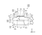
- FIG. 1 is an exemplary and schematic side view of the optical waveguide structure of the first embodiment.
- FIG. 2 is an exemplary and schematic front view of a part of the optical waveguide structure of the first embodiment.
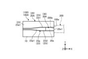
- FIG. 3 is an exemplary and schematic plan view of the optical waveguide structure of the first embodiment.
- FIG. 4 is an exemplary and schematic front view of a part of the optical waveguide structure of the second embodiment.
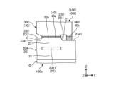
- FIG. 5 is an exemplary and schematic front view of a part of the optical waveguide structure of the third embodiment.
- FIG. 6 is an exemplary and schematic front view of a part of the optical waveguide structure of the fourth embodiment.
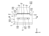
- FIG. 7 is an exemplary and schematic front view of a part of the optical waveguide structure of the fifth embodiment.
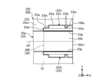
- FIG. 8 is a sectional view taken along line VIII-VIII in FIG.
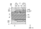
- FIG. 9 is an exemplary and schematic plan view of the waveguide layer of the optical waveguide structure of the fifth embodiment.
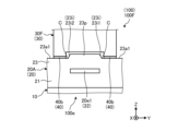
- FIG. 10 is an exemplary and schematic front view of a part of the optical waveguide structure of the sixth embodiment.
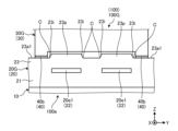
- FIG. 11 is an exemplary and schematic front view of a part of the optical waveguide structure of the seventh embodiment.
- FIG. 12 is an exemplary and schematic front view of a part of the optical waveguide structure of the eighth embodiment.
- FIG. 13 is an exemplary and schematic front view of a part of the optical waveguide structure of the ninth embodiment.
- Exemplary embodiments of the present invention are disclosed below.
- the configuration of the embodiment shown below, and the actions and results (effects) brought about by the configuration are examples.
- the present invention can be realized by configurations other than those disclosed in the following embodiments. Further, according to the present invention, it is possible to obtain at least one of various effects (including derivative effects) obtained by the configuration.
- the X direction is represented by an arrow X
- the Y direction is represented by an arrow Y
- the Z direction is represented by an arrow Z.
- the X direction, Y direction, and Z direction intersect each other and are orthogonal to each other.
- the X direction is also referred to as the longitudinal direction or extension direction
- the Y direction is also referred to as the lateral direction or width direction
- the Z direction is also referred to as the stacking direction or height direction.
- each figure is a schematic diagram for the purpose of explanation, and the scale and ratio of each figure and the actual thing do not necessarily match.
- FIG. 1 is a side view of the optical waveguide structure 100A (100) of the first embodiment.
- the optical waveguide structure 100 includes a base 10, a waveguide layer 20A (20), a member 30A (30), and an adhesive 40.
- the base 10, waveguide layer 20, adhesive 40, and member 30 are laminated in the Z direction.
- the member 30 is provided on the side opposite to the base 10 with respect to the end 20e of the waveguide layer 20 in the X direction, that is, the end 20e in the longitudinal direction.
- the adhesive 40 joins the end 20e of the waveguide layer 20 and the member 30.
- the base 10 is an example of a first member. Adhesive 40 may also be referred to as a bonding agent.
- the base 10 may also be referred to as a substrate.
- the base 10 and the waveguide layer 20 constitute a PLC (planar lightwave circuit).
- the end surface 100e of the optical waveguide structure 100 and the end surface 200e of another optical structure 200 are joined with an adhesive or the like while facing each other, so that the optical waveguide structure 100 and the optical Structure 200 is integrated.
- the end surface 100e is configured as an end surface of the base 10, the waveguide layer 20, the adhesive 40, and the member 30.
- An end surface 20e1 of the waveguide layer 20 located within the end surface 100e of the optical waveguide structure 100 is an input end or an output end of light.
- the optical structure 200 is, for example, an optical fiber support structure, an optical sensor, etc., but is not limited thereto.
- the waveguide layer 20 of the optical waveguide structure 100 and the waveguide (not shown) of the optical structure 200 are optically connected.
- the optical waveguide structure 100 did not have the member 30 and the adhesive 40 but only the base 10 and the waveguide layer 20, the structure would be different from the structure with the member 30 and the adhesive 40. , the thickness in the Z direction becomes thinner. Therefore, there is a possibility that the subassembly of the optical waveguide structure 100 and the optical structure 200 becomes easy to bend and break at the joint portion of the end surfaces 100e and 200e. Furthermore, since the end surface 100e is narrow, there is also a possibility that the tensile strength will be insufficient.
- the optical waveguide structure 100 of the present embodiment has the member 30 facing the optical structure 200 and the adhesive 40 on the side opposite to the base 10 with respect to the end 20e of the waveguide layer 20.
- the subassembly in which the optical waveguide structure 100 and the optical structure 200 are integrated has lower bending rigidity, bending strength, shear strength, and tensile strength. Easy to improve mechanical properties.
- Member 30 is an example of a second member.
- the member 30 functions as a reinforcing member, and may also be referred to as an upper plate, a yato, or the like.
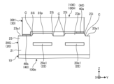
- FIG. 2 is a front view of the optical waveguide structure 100A of the first embodiment and a part of the end face 100e of (100).
- the base 10 is, for example, a silicon substrate. As shown in FIGS. 1 and 2, the base 10 intersects and is perpendicular to the Z direction, and extends in the X and Y directions.
- Base 10 has a surface 10a.
- the surface 10a is an end face in the Z direction.
- the surface 10a faces the Z direction, intersects and is perpendicular to the Z direction, and extends in the X and Y directions.
- the Z direction is an example of the first direction.
- Surface 10a is an example of a first surface.
- the waveguide layer 20 includes a first cladding layer 21, a core layer 22, and a second cladding layer 23.
- the first cladding layer 21, the core layer 22, and the second cladding layer 23 are laminated in this order on the surface 10a by a CVD method (CVD: chemical vapor deposition).
- the first cladding layer 21 covers the surface 10a of the base 10 with a substantially constant thickness t1 in the Z direction.
- the first cladding layer 21 intersects and is perpendicular to the Z direction, and extends in the X direction and the Y direction.
- the core layer 22 is laminated on a portion of the upper surface 21a of the first cladding layer 21 with a substantially constant thickness t2 in the Z direction.
- the first cladding layer 21 is interposed between the core layer 22 and the surface 10a of the base 10. That is, the core layer 22 is located away from the surface 10a in the Z direction.
- the core layer 22 extends in the X direction with a predetermined width w1.
- the X direction is an example of the second direction.
- the second cladding layer 23 is laminated on the first cladding layer 21 and the core layer 22 with a substantially constant thickness t3 in the Z direction.
- the core layer 22 is laminated on the upper surface 21a of the first cladding layer 21. Therefore, before the second cladding layer 23 is laminated, the core layer 22 protrudes from the upper surface 21a in the Z direction by a thickness t2. Therefore, the second cladding layer 23 laminated on the first cladding layer 21 and the core layer 22 having such a shape and arrangement includes a portion 23a formed on the upper surface 21a apart from the core layer 22, and a portion 23a formed on the upper surface 21a of the core layer 22.
- a protrusion 23p is formed in a portion that includes a portion 23b formed on the core layer 22 and is on the opposite side of the base 10 with respect to the core layer 22.
- the protruding portion 23p is a part (end portion in the Z direction) of the portion 23b.
- the top surface 23p1 of the protrusion 23p that is, the top surface 23p1 located at the end of the portion 23b in the Z direction, faces the Z direction, intersects and is perpendicular to the Z direction, and extends in the X and Y directions. There is.
- the surface 23a1 located at the end of the portion 23a in the Z direction also faces the Z direction, intersects and is perpendicular to the Z direction, and extends in the X direction and the Y direction.
- the top surface 23p1 protrudes from the surface 23a1 in the Z direction at approximately the same height as the thickness t2 of the core layer 22.
- the surface 23a1 is an example of a peripheral portion of the protrusion 23p, and may also be referred to as a base surface or a flat surface.
- the first cladding layer 21 and the second cladding layer 23 constitute a cladding layer that surrounds the core layer 22 on the surface 10a of the base 10 and extends in the X direction.
- the cladding layers are made of, for example, a silica-based glass material.
- the core layer 22 is made of, for example, a silica-based glass material having a higher refractive index than the refractive index of the first cladding layer 21 and the second cladding layer 23.
- the core layer 22 may be made of, for example, quartz glass containing germania (GeO2) or zirconia (ZrO2) as a dopant that increases the refractive index.
- the member 30 is made of, for example, a quartz glass material, a borosilicate glass material, or the like.
- the adhesive 40 is made of, for example, epoxy resin, acrylic resin, vinyl resin, or the like.
- an inclined portion 23i is formed at the boundary between the protruding portion 23p and the surface 23a1.
- the inclined part 23i includes an inclined part 23i1 located at the end of the protruding part 23p in the Y direction, and an inclined part 23i2 located at the opposite end of the protruding part 23p in the Y direction.
- the slope portion 23i1 is an example of a first slope portion
- the slope portion 23i2 is an example of a second slope portion.
- the Y direction is an example of the third direction.
- FIG. 3 is a plan view of the optical waveguide structure 100A (100) of the first embodiment.
- the protrusion 23p is formed on the opposite side of the base 10 with respect to the core layer 22. Therefore, the planar shape of the protrusion 23p as shown in FIG. 3 approximately corresponds to the planar shape of the core layer 22.
- the protrusion 23p extends in the X direction, and the width of the protrusion 23p in the Y direction changes. That is, the core layer 22 extends in the X direction, and the width of the core layer 22 in the Y direction changes.
- the protrusion 23p has a section where the width in the Y direction increases as it goes in the X direction, and the width in the Y direction at the end of the protrusion 23p in the X direction is in the opposite direction to the X direction of the protrusion 23p. It is wider than the width in the Y direction at the end. That is, the core layer 22 has a section where the width in the Y direction increases as it goes in the X direction, and the width in the Y direction at the end of the core layer 22 in the X direction is equal to the width in the opposite direction to the X direction. It is wider than the width in the Y direction at the end.
- the planar shape of the protrusion 23p that is, the planar shape of the core layer 22, is not limited to that shown in FIG. 3, and for example, the width may be constant, branched, or curved.
- the thicknesses t1 and t3 (see FIG. 2) of the first cladding layer 21 and the second cladding layer 23 are, for example, 10 [ ⁇ m]
- the thickness t2 (see FIG. 2) of the core layer 22 is, for example, It can be set to 3 [ ⁇ m].
- the width w1 (see FIG. 2) of the core layer 22 can be set to, for example, 1 [mm] or more.
- the inventors found that when the thickness t3 of the second cladding layer 23 is thin as in the above-described configuration, the slope of the slope portion 23i with respect to the surface 23a1 and the top surface 23p1 is lower than when the second cladding layer 23 is thick. It was found that the curve becomes steeper. This is because when the second cladding layer 23 is laminated by the CVD method, if the thickness t3 of the second cladding layer 23 is relatively thick, the inclination occurs corresponding to the inclination of the edge of the core layer 22 in the width direction.
- the inventors found that when a fluid adhesive 40 before solidification is applied onto such a steep slope 23i, the corner C between the slope 23i and the surface 23a1 (see FIG. (see), the adhesive 40 may not enter the corner C, and a gap may be created between the corner C and the adhesive 40, which may reduce the bonding strength between the waveguide layer 20 and the member 30 due to the adhesive 40, or reduce the bonding strength. It was found that there is a possibility that individual differences may occur.
- the bonding strength between the waveguide layer 20 and the member 30 decreases, the bonding strength between the optical waveguide structure 100 and the optical structure 200 also decreases, and the mechanical properties of the subassembly of the optical waveguide structure 100 and the optical structure 200 also decrease. It will be damaged.
- the adhesive 40 is not applied to the inclined part 23i, but is applied to the inclined part 23i, particularly the corner C between the inclined part 23i and the surface 23a1, that is, the root part of the protruding part 23p.
- the waveguide layer 20 (second cladding layer 23) and the member 30 are bonded.
- the adhesive 40 is provided on the top surface 23p1 of the protrusion 23p, and joins the top surface 23p1 and the bottom surface 30a of the member 30.
- the configuration in which the member 30A is located on the protrusion 23p as in this embodiment is more effective when the width w1 of one core layer 22 is wide, such as 1 mm or more.
- the fact that the second cladding layer 23 was laminated by the CVD method that produces the above-mentioned steep slope portion 23i can be identified by the fact that the second cladding layer 23 contains tetraethoxysilane.
- the steep slope portion 23i in which the adhesive 40 is difficult to enter the corner C is formed when the thickness t3 of the second cladding layer 23 is, for example, 15 [ ⁇ m] or less. It was found that this phenomenon is more likely to occur when the thickness is thin. That is, the configuration of this embodiment is more effective when the thickness t3 of the second cladding layer 23 is 15 [ ⁇ m] or less.
- FIG. 4 is a front view of the optical waveguide structure 100B (100) of the second embodiment. As will become clear when FIG. 4 is compared with FIG. 2, the shape of the member 30B (30) is different from the member 30A (30) of the first embodiment.
- the width in the Y direction of the member 30B at a position away from the bonded portion with the adhesive 40 in the Z direction is wider than the width in the Y direction of the bonded portion.
- the area of the end surface 100e joined to the end surface 200e of another optical structure 200 can be made larger, and the joining strength with the optical structure 200 can be increased accordingly.
- FIG. 5 is a front view of an optical waveguide structure 100C (100) of the third embodiment.
- the member 30C (30) and the waveguide layer 20 are bonded to each other by adhesives 40 provided at a plurality of locations (two locations in this example).
- the adhesive 40 includes an adhesive 40a that joins the protrusion 23p and the member 30C, and an adhesive 40b that joins the surface 23a1 and the member 30C at a position shifted from the slope 23i and away from the corner C. I'm here.
- the inclined portion 23i is located between the plurality of adhesives 40a and 40b.
- the adhesive 40a is an example of a first adhesive
- the adhesive 40b is an example of a second adhesive.
- the adhesive 40 is provided at two locations, the bonding strength between the member 30C and the waveguide layer 20 can be further increased. Furthermore, since the adhesive 40 is provided at two locations separated in the Y direction, the member 30C has a wider width in the Y direction, so the area of the end surface 100e to be joined to the end surface 200e of the optical structure 200 is increased. Therefore, the bonding strength with the optical structure 200 can be increased accordingly.
- FIG. 6 is a front view of an optical waveguide structure 100D (100) of the fourth embodiment.
- the member 30D (30) and the waveguide layer 20 are bonded to each other by adhesives 40 provided at a plurality of locations (three locations in this example).
- the adhesive 40 includes an adhesive 40a that joins the protrusion 23p and the member 30D, and two adhesives 40b that join the surface 23a1 and the member 30C at a position shifted from the slope 23i and away from the corner C. Contains.
- two inclined parts 23i1 and 23i2 are located between two adhesives 40b.
- the adhesive 40 is provided at three locations, the bonding strength between the member 30C and the waveguide layer 20 can be further increased. Furthermore, since the adhesive 40 is provided at three locations separated in the Y direction, the member 30C has a wider width in the Y direction, so the area of the end surface 100e to be joined to the end surface 200e of the optical structure 200 is increased. Therefore, the bonding strength with the optical structure 200 can be increased accordingly.
- FIG. 7 is a front view of an optical waveguide structure 100E (100) of the fifth embodiment.
- the waveguide layer 20E (20) of this embodiment is provided with dummy layers 24A and 24B (24) that are lined up with the core layer 22 in the Y direction.
- the dummy layer 24 is laminated in the same process as the core layer 22.
- the dummy layer 24 is made of the same components as the core layer 22 and has the same thickness t2 (see FIG. 2) as the core layer 22.
- a second cladding layer 23 is interposed between the dummy layer 24 and the core layer 22. Therefore, light hardly leaks from the core layer 22 to the dummy layer 24.
- the dummy layer 24A shifted in the Y direction with respect to the core layer 22 is an example of a first dummy layer
- the dummy layer 24B shifted in the opposite direction of the Y direction with respect to the core layer 22 is a second dummy layer. This is an example.
- the protrusion 23p is formed to cover the core layer 22 and the two dummy layers 24. That is, the protrusion 23p includes a portion located on the opposite side of the base 10 with respect to the dummy layer 24.
- the width of the protrusion 23p in the Y direction can be made wider.
- the width of the adhesive 40 in the Y direction can be increased, and the bonding strength between the protrusion 23p and the member 30E can be increased accordingly.
- the member 30E since the width of the protrusion 23p and the adhesive 40 is increased, the member 30E has a wider width in the Y direction, so the area of the end surface 100e joined to the end surface 200e of the optical structure 200 is increased. Therefore, the bonding strength with the optical structure 200 can be increased accordingly.
- a groove 23g is formed on the top surface 23p1 at a position aligned with the interval between the core layer 22 and the dummy layer 24 in the Z direction.
- the depth of the groove 23g is set to be shallower than the height of the protrusion 23p, that is, the thickness t2 of the core layer 22, and is set to such an extent that the adhesive 40 can enter therein. Therefore, the adhesive 40 does not enter into the groove 23g, and a gap is created between the adhesive 40 and the protrusion 23p, and the bonding strength between the waveguide layer 20 and the member 30E by the adhesive 40 is reduced. This situation can be avoided.
- FIG. 8 is a sectional view taken along line VIII-VIII in FIG. 7. As shown in FIG. 8 when the cross section is viewed in the opposite direction to the Z direction, a concave shape 24b and a convex shape 24a are provided on the edge of the dummy layer 24 on the opposite side to the core layer 22.
- the concave shape 24b and the convex shape 24a are formed by alternately providing edges extending in the X direction and edges extending in the Y direction in a plan view of FIG. If light were to leak from the core layer 22 to the dummy layer 24, it would be undesirable for the leaked light to be transmitted within the dummy layer 24 in the X direction toward the optical structure 200.
- the concave shape 24b and the convex shape 24a are provided at the position of the dummy layer 24 in the waveguide layer 20 so that the effective refractive index changes discontinuously along the X direction.
- the light transmitted through the dummy layer 24 leaks out of the dummy layer 24 from the concave shape 24b and the convex shape 24a.
- the width w2 of the convex shape 24a in the Y direction is 500 [ ⁇ m]
- the width w3 of the concave shape 24b in the Y direction is 250 [ ⁇ m].
- the length L1 of the convex shape 24a in the X direction is 300 [ ⁇ m] or more and 2000 [ ⁇ m] or less, and the length L2 of the concave shape 24b in the X direction is 200 [ ⁇ m] or more and 1000 [ ⁇ m] or less. . Further, the distance d1 between the core layer 22 and the dummy layer 24 is 10 [ ⁇ m]. However, the values of width w2, width w3, length L1, length L2, and distance d1 are only examples, and are not limited to the above values.
- the concave shape 24b and the convex shape 24a are examples of leakage portions.
- the optical waveguide structure 100E of this embodiment has a plane-symmetric structure with respect to the virtual plane VP.
- the virtual plane VP is along the X direction and the Z direction and is orthogonal to the Y direction. Therefore, the dummy layer 24B also has a structure that is plane symmetrical to the dummy layer 24A. Therefore, the same effect as the dummy layer 24A can be obtained by the dummy layer 24B as well.
- FIG. 9 is a plan view of the waveguide layer 20E of the optical waveguide structure 100E, in other words, a plan view showing a state before the member 30E is placed on the waveguide layer 20E in the manufacturing process of the optical waveguide structure 100E.
- a protrusion 23p corresponding to the core layer 22 and the dummy layer 24 is formed at the end of the waveguide layer 20 in the Z direction. That is, the protrusion 23p has a shape corresponding to the concave shape 24b and the convex shape 24a in a plan view seen in the opposite direction to the Z direction.
- the inclined part 23i1 located at the end of the protrusion 23p in the Y direction and the inclined part 23i2 located at the opposite end of the Y direction are respectively a section 23ia extending in the X direction and a section extending in the Y direction. 23ib.
- these sections 23ia and 23ib can be used for positioning the member 30E. That is, the sections 23ia and 23ib of the inclined portion 23i are examples of alignment markers.
- FIG. 10 is a front view of an optical waveguide structure 100F (100) of the sixth embodiment.
- the member 30F (30) and the waveguide layer 20 are bonded to each other by the adhesive 40 provided at a plurality of locations (two locations in this example).
- the adhesive 40 includes two adhesives 40b that join the surface 23a1 and the member 30F at a position offset from the inclined portion 23i and away from the corner C.
- two inclined parts 23i1 and 23i2 are located between two adhesives 40b.
- the adhesive 40 is provided at two locations, the bonding strength between the member 30F and the waveguide layer 20 can be further increased. Furthermore, since the adhesive 40 is provided at two locations separated in the Y direction, the member 30F has a wider width in the Y direction, so the area of the end surface 100e to be joined to the end surface 200e of the optical structure 200 is increased. Therefore, the bonding strength with the optical structure 200 can be increased accordingly. Note that, as is clear from the example of FIG. 10, it is not essential that the member 30F (30) and the protruding portion 23p be joined by the adhesive 40.
- FIG. 11 is a front view of an optical waveguide structure 100G (100) of the seventh embodiment.
- the member 30G (30) and the waveguide layer 20G (20) are bonded to each other by the adhesive 40 provided at a plurality of locations (two locations in this example).
- the adhesive 40 includes two adhesives 40b that join the surface 23a1 and the member 30G at a position offset from the inclined portion 23i and away from the corner C.
- two protrusions 23p that is, four inclined portions 23i, are located between the two adhesives 40b.
- the adhesive 40 is provided at two locations, the bonding strength between the member 30G and the waveguide layer 20 can be further increased. Furthermore, since the adhesive 40 is provided at two locations separated in the Y direction, the member 30G has a wider width in the Y direction, so the area of the end surface 100e to be joined to the end surface 200e of the optical structure 200 is increased. Therefore, the bonding strength with the optical structure 200 can be increased accordingly. Moreover, in this embodiment, one member 30G functions as a reinforcing member corresponding to the plurality of protrusions 23p (core layer 22).
- the number of parts can be further reduced, and the labor and cost of manufacturing can be reduced. It also has the advantage of being able to.
- FIG. 12 is a front view of an optical waveguide structure 100H (100) of the eighth embodiment.
- the member 30H (30) and the waveguide layer 20 are bonded to each other by the adhesive 40 provided at a plurality of locations (two locations in this example).
- the adhesive 40 includes an adhesive 40a that joins the protrusion 23p and the member 30H, and two adhesives 40b that join the surface 23a1 and the member 30H at a position shifted from the slope 23i and away from the corner C. Contains.
- three inclined portions 23i are located between the two adhesives 40a and 40b.
- the adhesive 40 is provided at two locations, the bonding strength between the member 30H and the waveguide layer 20 can be further increased. Furthermore, since the adhesive 40 is provided at two locations separated in the Y direction, the member 30H has a wider width in the Y direction, so the area of the end surface 100e to be joined to the end surface 200e of the optical structure 200 is increased. Therefore, the bonding strength with the optical structure 200 can be increased accordingly. Further, in this embodiment as well, since one member 30H is shared by a plurality of protrusions 23p (core layer 22), the number of parts can be further reduced, and the labor and cost of manufacturing can be reduced. Can be done.
- FIG. 13 is a front view of an optical waveguide structure 100I (100) of the ninth embodiment.
- the member 30I (30) and the waveguide layer 20 are bonded to each other by the adhesive 40 provided at a plurality of locations (in this example, two or more locations).
- the adhesive 40 includes a plurality of adhesives 40a that join the protrusion 23p and the member 30I.
- two inclined portions 23i are located between two adhesives 40a adjacent to each other in the Y direction.
- the member 30I is provided to cover two or more protrusions 23p.
- the adhesive 40 is provided at two or more locations, the bonding strength between the member 30I and the waveguide layer 20 can be further increased. Furthermore, since the adhesive 40 is provided at two or more locations separated in the Y direction, the member 30I has a wider width in the Y direction, so the area of the end surface 100e to be joined to the end surface 200e of the optical structure 200 is reduced. It can be made larger, and the bonding strength with the optical structure 200 can be increased accordingly. Further, in this embodiment as well, since one member 30I is shared by a plurality of protrusions 23p (core layer 22), the number of parts can be further reduced, and the labor and cost of manufacturing can be reduced. Can be done.
- the optical waveguide structure is a PLC, but it is not limited to this, and the optical waveguide structure may be, for example, a SiPh waveguide, an InP waveguide, or a SiN waveguide.
- the present invention can be utilized for optical waveguide structures.
Landscapes
- Physics & Mathematics (AREA)
- General Physics & Mathematics (AREA)
- Optics & Photonics (AREA)
- Engineering & Computer Science (AREA)
- Microelectronics & Electronic Packaging (AREA)
- Optical Couplings Of Light Guides (AREA)
- Optical Integrated Circuits (AREA)
Abstract
Description
図1は、第1実施形態の光導波路構造100A(100)の側面図である。図1に示されるように、光導波路構造100は、ベース10と、導波路層20A(20)と、部材30A(30)と、接着剤40と、を備えている。ベース10、導波路層20、接着剤40、および部材30は、Z方向に積層されている。部材30は、導波路層20のX方向の端部20e、すなわち長手方向の端部20eに対して、ベース10とは反対側に設けられている。接着剤40は、導波路層20の端部20eと部材30とを接合している。ベース10は、第一部材の一例である。接着剤40は、接合剤とも称されうる。ベース10は、基板とも称されうる。また、ベース10および導波路層20は、PLC(planar lightwave circuit)を構成している。
図4は、第2実施形態の光導波路構造100B(100)の正面図である。図4を図2と比較すれば明らかとなるように、部材30B(30)の形状が、第1実施形態の部材30A(30)と相違している。
図5は、第3実施形態の光導波路構造100C(100)の正面図である。本実施形態では、部材30C(30)と導波路層20とは、複数箇所(この例では2箇所)に設けられた接着剤40によって接合されている。接着剤40は、突出部23pと部材30Cとを接合する接着剤40aと、傾斜部23iからずれるとともに隅部Cから離れた位置で表面23a1と部材30Cとを接合する接着剤40bと、を含んでいる。この場合、複数の接着剤40a,40bの間に、傾斜部23iが位置している。接着剤40aは、第一接着剤の一例であり、接着剤40bは、第二接着剤の一例である。
図6は、第4実施形態の光導波路構造100D(100)の正面図である。本実施形態でも、部材30D(30)と導波路層20とは、複数箇所(この例では3箇所)に設けられた接着剤40によって接合されている。接着剤40は、突出部23pと部材30Dとを接合する接着剤40aと、傾斜部23iからずれるとともに隅部Cから離れた位置で表面23a1と部材30Cとを接合する二つの接着剤40bと、を含んでいる。また、本実施形態では、二つの接着剤40bの間に、二つの傾斜部23i1,23i2が位置している。
図7は、第5実施形態の光導波路構造100E(100)の正面図である。本実施形態の導波路層20E(20)には、Y方向においてコア層22と並んだダミー層24A,24B(24)が設けられている。
図10は、第6実施形態の光導波路構造100F(100)の正面図である。本実施形態でも、部材30F(30)と導波路層20とは、複数箇所(この例では2箇所)に設けられた接着剤40によって接合されている。接着剤40は、傾斜部23iからずれるとともに隅部Cから離れた位置で表面23a1と部材30Fとを接合する二つの接着剤40bを含んでいる。また、本実施形態では、二つの接着剤40bの間に、二つの傾斜部23i1,23i2が位置している。
図11は、第7実施形態の光導波路構造100G(100)の正面図である。本実施形態でも、部材30G(30)と導波路層20G(20)とは、複数箇所(この例では2箇所)に設けられた接着剤40によって接合されている。接着剤40は、傾斜部23iからずれるとともに隅部Cから離れた位置で表面23a1と部材30Gとを接合する二つの接着剤40bを含んでいる。また、本実施形態では、二つの接着剤40bの間に、二つの突出部23p、すなわち四つの傾斜部23iが、位置している。
図12は、第8実施形態の光導波路構造100H(100)の正面図である。本実施形態でも、部材30H(30)と導波路層20とは、複数箇所(この例では2箇所)に設けられた接着剤40によって接合されている。接着剤40は、突出部23pと部材30Hとを接合する接着剤40aと、傾斜部23iからずれるとともに隅部Cから離れた位置で表面23a1と部材30Hとを接合する二つの接着剤40bと、を含んでいる。また、本実施形態では、二つの接着剤40a,40bの間に、三つの傾斜部23iが位置している。
図13は、第9実施形態の光導波路構造100I(100)の正面図である。本実施形態でも、部材30I(30)と導波路層20とは、複数箇所(この例では2箇所以上)に設けられた接着剤40によって接合されている。接着剤40は、突出部23pと部材30Iとを接合する複数の接着剤40aを含んでいる。また、本実施形態では、Y方向に隣り合った二つの接着剤40aの間に、二つの傾斜部23iが位置している。部材30Iは、2個以上の突出部23pを覆うように設けられている。
10a…表面
20,20A,20E,20G…導波路層
20e…端部
20e1…端面
21…第一クラッド層
21a…上面
22…コア層
23…第二クラッド層
23a…部位
23b…部位
23a1…表面(周辺部分)
23g…溝
23i…傾斜部
23i1…傾斜部(第一傾斜部)
23i2…傾斜部(第二傾斜部)
23ia…区間
23ib…区間
23p…突出部
23p1…頂面
24…ダミー層
24A…ダミー層(第一ダミー層)
24B…ダミー層(第二ダミー層)
24a…凸部形状(漏洩部)
24b…凹部形状(漏洩部)
30,30A~30I…部材
30a…底面
40…接着剤
40a…接着剤(第一接着剤)
40b…接着剤(第二接着剤)
100,100A~100I…光導波路構造
100e…端面
200…光学構造
200e…端面
C…隅部
d1…距離
L1…長さ
L2…長さ
t1…厚さ
t2…厚さ
t3…厚さ
w1…幅
w2…幅
w3…幅
VP…仮想平面
X…方向(第二方向)
Y…方向(第三方向)
Z…方向(第一方向)
Claims (15)
- 第一方向を向いた第一面を有した第一部材と、
前記第一面から離れた位置で前記第一方向と交差した第二方向に延びたコア層と、前記第一面上で前記コア層を取り囲むクラッド層であって少なくとも前記コア層に対して前記第一部材の反対側となる部位でその周辺部分に対して前記第一方向に突出した突出部を有したクラッド層と、前記突出部と前記周辺部分との境界に設けられた傾斜部と、を有した導波路層と、
前記導波路層の長手方向の端部に対して前記第一部材とは反対側に設けられた第二部材と、
前記傾斜部からずれた位置で、前記クラッド層と前記第二部材とを接合した接着剤と、
を備えた、光導波路構造。 - 前記導波路層は、前記接着剤として、前記突出部と前記第二部材とを接合した第一接着剤を有した、請求項1に記載の光導波路構造。
- 前記導波路層は、前記接着剤として、前記周辺部分と前記第二部材とを接合した第二接着剤を有した、請求項1に記載の光導波路構造。
- 前記導波路層は、前記接着剤として、前記突出部と前記第二部材とを接合した第一接着剤と、前記周辺部分と前記第二部材とを接合した第二接着剤と、を有した、請求項1に記載の光導波路構造。
- 前記導波路層は、前記接着剤として、前記クラッド層と前記第二部材とを接合する複数の接着剤を有した、請求項1に記載の光導波路構造。
- 前記複数の接着剤の間に、前記傾斜部が位置した、請求項5に記載の光導波路構造。
- 前記複数の接着剤の間に、前記傾斜部として複数の傾斜部が位置した、請求項5に記載の光導波路構造。
- 前記クラッド層は、前記傾斜部として、前記突出部における前記第一方向および前記第二方向と交差した第三方向の端部に位置した第一傾斜部と、前記突出部における前記第三方向の反対方向の端部に位置した第二傾斜部と、を有し、
前記複数の接着剤の間に、前記第一傾斜部および前記第二傾斜部が位置した、請求項7に記載の光導波路構造。 - 前記導波路層は、前記第一方向および前記第二方向と交差した方向に間隔をあけて前記コア層と並んだダミー層を有し、
前記突出部は、前記ダミー層に対して前記第一部材とは反対側に位置した部位を含む、請求項2に記載の光導波路構造。 - 前記導波路層は、前記ダミー層として、前記コア層に対して前記第一方向および前記第二方向と交差した第三方向にずれた第一ダミー層と、前記コア層に対して前記第三方向の反対方向にずれた第二ダミー層と、を有した、請求項9に記載の光導波路構造。
- 前記ダミー層は、光を漏洩する漏洩部を有した、請求項10に記載の光導波路構造。
- 前記ダミー層は、前記漏洩部として、前記ダミー層の前記コア層とは反対側の縁に、前記第一方向の反対方向に見た場合における凹部形状または凸部形状が設けられた、請求項11に記載の光導波路構造。
- 前記コア層上に積層される前記クラッド層の前記第一方向における厚さは、15[μm]以下である、請求項1~12のうちいずれか一つに記載の光導波路構造。
- 前記クラッド層は、テトラエトキシシランを含む、請求項1~12のうちいずれか一つに記載の光導波路構造。
- 前記コア層の、前記第一方向および前記第二方向と交差した第三方向における幅は、1[mm]以上である、請求項1~12のうちいずれか一つに記載の光導波路構造。
Priority Applications (2)
| Application Number | Priority Date | Filing Date | Title |
|---|---|---|---|
| CN202380055850.9A CN119790337A (zh) | 2022-08-10 | 2023-08-09 | 光波导结构 |
| US19/046,779 US20250180807A1 (en) | 2022-08-10 | 2025-02-06 | Optical waveguide structure |
Applications Claiming Priority (2)
| Application Number | Priority Date | Filing Date | Title |
|---|---|---|---|
| JP2022-128408 | 2022-08-10 | ||
| JP2022128408A JP2024025173A (ja) | 2022-08-10 | 2022-08-10 | 光導波路構造 |
Related Child Applications (1)
| Application Number | Title | Priority Date | Filing Date |
|---|---|---|---|
| US19/046,779 Continuation US20250180807A1 (en) | 2022-08-10 | 2025-02-06 | Optical waveguide structure |
Publications (1)
| Publication Number | Publication Date |
|---|---|
| WO2024034641A1 true WO2024034641A1 (ja) | 2024-02-15 |
Family
ID=89851663
Family Applications (1)
| Application Number | Title | Priority Date | Filing Date |
|---|---|---|---|
| PCT/JP2023/029112 Ceased WO2024034641A1 (ja) | 2022-08-10 | 2023-08-09 | 光導波路構造 |
Country Status (4)
| Country | Link |
|---|---|
| US (1) | US20250180807A1 (ja) |
| JP (1) | JP2024025173A (ja) |
| CN (1) | CN119790337A (ja) |
| WO (1) | WO2024034641A1 (ja) |
Citations (9)
| Publication number | Priority date | Publication date | Assignee | Title |
|---|---|---|---|---|
| JPH0843675A (ja) * | 1994-08-02 | 1996-02-16 | Shin Etsu Chem Co Ltd | 光導波路 |
| JP2001242332A (ja) * | 2000-03-01 | 2001-09-07 | Nippon Telegr & Teleph Corp <Ntt> | 光導波路及びこれを用いた光導波路モジュール |
| JP2003240990A (ja) * | 2002-02-14 | 2003-08-27 | Fujitsu Ltd | 平面光導波路装置 |
| US20040126051A1 (en) * | 2001-01-25 | 2004-07-01 | Michel Bruel | Low-birefringent integrated optics structures |
| JP2009139474A (ja) * | 2007-12-04 | 2009-06-25 | Ntt Electornics Corp | 光導波回路チップ |
| JP2010122350A (ja) * | 2008-11-18 | 2010-06-03 | Nippon Telegr & Teleph Corp <Ntt> | 光導波路の作製方法 |
| JP2014238491A (ja) * | 2013-06-07 | 2014-12-18 | 日東電工株式会社 | 光電気混載モジュール |
| US20170184792A1 (en) * | 2014-01-31 | 2017-06-29 | Centre National De La Recherche Scientifique | Method for Producing a Ridge Optical Waveguide Having Low Coupling Losses Between the Ridge Optical Waveguide and an Optical Fibre, and a Ridge Optical Waveguide Made Using This Method |
| JP2019039948A (ja) * | 2017-08-22 | 2019-03-14 | 日東電工株式会社 | 光導波路、光電気混載基板および光電気混載モジュール |
-
2022
- 2022-08-10 JP JP2022128408A patent/JP2024025173A/ja active Pending
-
2023
- 2023-08-09 CN CN202380055850.9A patent/CN119790337A/zh active Pending
- 2023-08-09 WO PCT/JP2023/029112 patent/WO2024034641A1/ja not_active Ceased
-
2025
- 2025-02-06 US US19/046,779 patent/US20250180807A1/en active Pending
Patent Citations (9)
| Publication number | Priority date | Publication date | Assignee | Title |
|---|---|---|---|---|
| JPH0843675A (ja) * | 1994-08-02 | 1996-02-16 | Shin Etsu Chem Co Ltd | 光導波路 |
| JP2001242332A (ja) * | 2000-03-01 | 2001-09-07 | Nippon Telegr & Teleph Corp <Ntt> | 光導波路及びこれを用いた光導波路モジュール |
| US20040126051A1 (en) * | 2001-01-25 | 2004-07-01 | Michel Bruel | Low-birefringent integrated optics structures |
| JP2003240990A (ja) * | 2002-02-14 | 2003-08-27 | Fujitsu Ltd | 平面光導波路装置 |
| JP2009139474A (ja) * | 2007-12-04 | 2009-06-25 | Ntt Electornics Corp | 光導波回路チップ |
| JP2010122350A (ja) * | 2008-11-18 | 2010-06-03 | Nippon Telegr & Teleph Corp <Ntt> | 光導波路の作製方法 |
| JP2014238491A (ja) * | 2013-06-07 | 2014-12-18 | 日東電工株式会社 | 光電気混載モジュール |
| US20170184792A1 (en) * | 2014-01-31 | 2017-06-29 | Centre National De La Recherche Scientifique | Method for Producing a Ridge Optical Waveguide Having Low Coupling Losses Between the Ridge Optical Waveguide and an Optical Fibre, and a Ridge Optical Waveguide Made Using This Method |
| JP2019039948A (ja) * | 2017-08-22 | 2019-03-14 | 日東電工株式会社 | 光導波路、光電気混載基板および光電気混載モジュール |
Also Published As
| Publication number | Publication date |
|---|---|
| JP2024025173A (ja) | 2024-02-26 |
| CN119790337A (zh) | 2025-04-08 |
| US20250180807A1 (en) | 2025-06-05 |
Similar Documents
| Publication | Publication Date | Title |
|---|---|---|
| JP2011102819A (ja) | ハイブリッド集積光モジュール | |
| US11934011B2 (en) | Optical connecting structure | |
| CN103620893A (zh) | 光模块 | |
| JP2014048628A (ja) | 光接続部品 | |
| CN115774299A (zh) | 硅光芯片与平面波导阵列的封装方法及其封装结构 | |
| JP2024025173A (ja) | 光導波路構造 | |
| JP4471778B2 (ja) | 光導波路部材 | |
| US20240402444A1 (en) | Optical module | |
| US10215924B2 (en) | Optical interconnect with high alignment tolerance | |
| JP2025179381A (ja) | 光導波路部品 | |
| CN107430246B (zh) | 光传输模块 | |
| JP2020160261A (ja) | 導波路基板、光コネクタ、及び導波路基板の製造方法 | |
| US12222567B2 (en) | Optical circuit module | |
| JP5498175B2 (ja) | 光結合装置 | |
| CN116068702A (zh) | 一种光纤阵列组件及制作方法 | |
| US20250155644A1 (en) | Optical connection structure, optical module, and method for manufacturing optical module | |
| WO2022041021A1 (zh) | 一种光纤阵列单元与光通信设备 | |
| JP7244788B2 (ja) | 光ファイバ接続構造 | |
| WO2025182816A1 (ja) | 光部品 | |
| JP2015125286A (ja) | 光導波路デバイス、光導波路装置、光導波路デバイスを作製する方法 | |
| US20250116817A1 (en) | Multi-waveguide optical edge coupler having sub-wavelength structures | |
| WO2025244025A1 (ja) | 光モジュール | |
| WO2026047903A1 (ja) | 光接続構造 | |
| WO2018186037A1 (ja) | 光ファイバ部材及び光ファイバ保持具 | |
| JP2018180046A (ja) | 光ファイバ部材 |
Legal Events
| Date | Code | Title | Description |
|---|---|---|---|
| 121 | Ep: the epo has been informed by wipo that ep was designated in this application |
Ref document number: 23852603 Country of ref document: EP Kind code of ref document: A1 |
|
| WWE | Wipo information: entry into national phase |
Ref document number: 202380055850.9 Country of ref document: CN |
|
| NENP | Non-entry into the national phase |
Ref country code: DE |
|
| WWP | Wipo information: published in national office |
Ref document number: 202380055850.9 Country of ref document: CN |
|
| 122 | Ep: pct application non-entry in european phase |
Ref document number: 23852603 Country of ref document: EP Kind code of ref document: A1 |