WO2024029410A1 - 反射型マスクブランク及び反射型マスク - Google Patents
反射型マスクブランク及び反射型マスク Download PDFInfo
- Publication number
- WO2024029410A1 WO2024029410A1 PCT/JP2023/027272 JP2023027272W WO2024029410A1 WO 2024029410 A1 WO2024029410 A1 WO 2024029410A1 JP 2023027272 W JP2023027272 W JP 2023027272W WO 2024029410 A1 WO2024029410 A1 WO 2024029410A1
- Authority
- WO
- WIPO (PCT)
- Prior art keywords
- absorption layer
- reflective mask
- less
- pattern
- film
- Prior art date
- Legal status (The legal status is an assumption and is not a legal conclusion. Google has not performed a legal analysis and makes no representation as to the accuracy of the status listed.)
- Ceased
Links
Images


Classifications
-
- G—PHYSICS
- G03—PHOTOGRAPHY; CINEMATOGRAPHY; ANALOGOUS TECHNIQUES USING WAVES OTHER THAN OPTICAL WAVES; ELECTROGRAPHY; HOLOGRAPHY
- G03F—PHOTOMECHANICAL PRODUCTION OF TEXTURED OR PATTERNED SURFACES, e.g. FOR PRINTING, FOR PROCESSING OF SEMICONDUCTOR DEVICES; MATERIALS THEREFOR; ORIGINALS THEREFOR; APPARATUS SPECIALLY ADAPTED THEREFOR
- G03F1/00—Originals for photomechanical production of textured or patterned surfaces, e.g., masks, photo-masks, reticles; Mask blanks or pellicles therefor; Containers specially adapted therefor; Preparation thereof
- G03F1/22—Masks or mask blanks for imaging by radiation of 100nm or shorter wavelength, e.g. X-ray masks, extreme ultraviolet [EUV] masks; Preparation thereof
- G03F1/24—Reflection masks; Preparation thereof
-
- G—PHYSICS
- G03—PHOTOGRAPHY; CINEMATOGRAPHY; ANALOGOUS TECHNIQUES USING WAVES OTHER THAN OPTICAL WAVES; ELECTROGRAPHY; HOLOGRAPHY
- G03F—PHOTOMECHANICAL PRODUCTION OF TEXTURED OR PATTERNED SURFACES, e.g. FOR PRINTING, FOR PROCESSING OF SEMICONDUCTOR DEVICES; MATERIALS THEREFOR; ORIGINALS THEREFOR; APPARATUS SPECIALLY ADAPTED THEREFOR
- G03F1/00—Originals for photomechanical production of textured or patterned surfaces, e.g., masks, photo-masks, reticles; Mask blanks or pellicles therefor; Containers specially adapted therefor; Preparation thereof
- G03F1/26—Phase shift masks [PSM]; PSM blanks; Preparation thereof
- G03F1/32—Attenuating PSM [att-PSM], e.g. halftone PSM or PSM having semi-transparent phase shift portion; Preparation thereof
-
- G—PHYSICS
- G03—PHOTOGRAPHY; CINEMATOGRAPHY; ANALOGOUS TECHNIQUES USING WAVES OTHER THAN OPTICAL WAVES; ELECTROGRAPHY; HOLOGRAPHY
- G03F—PHOTOMECHANICAL PRODUCTION OF TEXTURED OR PATTERNED SURFACES, e.g. FOR PRINTING, FOR PROCESSING OF SEMICONDUCTOR DEVICES; MATERIALS THEREFOR; ORIGINALS THEREFOR; APPARATUS SPECIALLY ADAPTED THEREFOR
- G03F1/00—Originals for photomechanical production of textured or patterned surfaces, e.g., masks, photo-masks, reticles; Mask blanks or pellicles therefor; Containers specially adapted therefor; Preparation thereof
- G03F1/38—Masks having auxiliary features, e.g. special coatings or marks for alignment or testing; Preparation thereof
- G03F1/48—Protective coatings
-
- G—PHYSICS
- G03—PHOTOGRAPHY; CINEMATOGRAPHY; ANALOGOUS TECHNIQUES USING WAVES OTHER THAN OPTICAL WAVES; ELECTROGRAPHY; HOLOGRAPHY
- G03F—PHOTOMECHANICAL PRODUCTION OF TEXTURED OR PATTERNED SURFACES, e.g. FOR PRINTING, FOR PROCESSING OF SEMICONDUCTOR DEVICES; MATERIALS THEREFOR; ORIGINALS THEREFOR; APPARATUS SPECIALLY ADAPTED THEREFOR
- G03F1/00—Originals for photomechanical production of textured or patterned surfaces, e.g., masks, photo-masks, reticles; Mask blanks or pellicles therefor; Containers specially adapted therefor; Preparation thereof
- G03F1/54—Absorbers, e.g. of opaque materials
Definitions
- the present invention relates to a reflective mask blank used in extreme ultraviolet (EUV) lithography in semiconductor manufacturing and the like, and a reflective mask using the same.
- EUV extreme ultraviolet
- a reflective mask used in EUV lithography has a mask pattern made of an absorption layer that absorbs EUV light on a multilayer reflective film that reflects EUV light with a short wavelength of about 13.5 nm.
- a reflective mask has a thick absorption layer, dimensional errors in the transferred pattern are likely to occur due to so-called shadowing, in which obliquely incident (usually at an incident angle of 6 degrees) EUV light and its reflected light are blocked.
- phase shift mask technology improves the contrast of the edge portion of the transferred pattern by absorbing EUV light and using an absorption layer formed so that the reflected light has a different phase from the reflected light from the multilayer reflective film. Development is also underway.
- a material or shape that has a different refractive index or transmittance than the transmission part is added to the transmission part of the mask pattern, and the phase of light in this part is changed to improve the resolution. It is something that improves.
- the transmitted diffracted lights having a phase difference interfere with each other, and the light intensity decreases.
- the contrast of the transferred pattern is improved, and as a result, the depth of focus during transfer is expanded and the transfer accuracy is improved.
- a halftone mask which is a type of transmission phase shift mask, has a thin film semi-transparent to exposure light formed in a portion that changes the phase of transmitted light.
- Halftone masks improve the resolution of pattern edges by attenuating the transmittance to about a few percent (usually about 2.5 to 15.0% of the light transmitted through the substrate) and changing the phase. By doing so, the transfer accuracy can be improved. Note that, in principle, the best phase difference is 180°, but it is known that an effect of improving resolution can be obtained if the phase difference is substantially about 175 to 185°.
- phase difference the phase difference in a conventional reflective mask is generally designed so that the phase difference is around 180° (almost inverted) (for example, see Patent Document 1).
- the absorption layer of a reflective mask has a phase difference of 180 mm based on the refractive index (hereinafter sometimes referred to as n) and extinction coefficient (hereinafter sometimes referred to as k) of the constituent materials.
- n refractive index
- k extinction coefficient
- LSIs large-scale integrated circuits
- DRAM Dynamic Random Access Memory
- MOS transistors and resistors are becoming rapidly miniaturized, and as a result, wiring lines and contact holes for MOS transistors and resistors are reaching a level that is close to the limit of exposure technology. It has become even more miniaturized.
- DRAM Dynamic Random Access Memory
- NA numerical aperture
- the present invention was made in view of these circumstances, and provides a reflective mask for EUV lithography that can form a transfer pattern with high dimensional accuracy in a fine hole pattern, and a reflective mask blank used therein.
- the purpose is to provide.
- the present invention can be applied to fine hole-like patterns in an absorbing layer with high dimensional accuracy when the phase difference between the reflected light from the multilayer reflective film and the reflected light from the absorbing layer is larger than before. This is based on the discovery that it is possible to form a transfer pattern.
- the present invention is as follows.
- a reflective mask blank for EUV lithography in which a multilayer reflective film that reflects EUV light and an absorption layer that absorbs EUV light are laminated in this order from the substrate side on a substrate, and the absorption layer has a refractive index of less than 0.94 for EUV light with a wavelength of 13.5 nm, and an extinction coefficient of 0.060 or less, and is A reflective mask blank, wherein the phase difference between the reflected light from the surface of the absorption layer and the reflected light from the surface of the absorption layer is 220 to 320°.
- the absorption layer contains tantalum (Ta), tungsten (W), chromium (Cr), molybdenum (Mo), niobium (Nb), osmium (Os), iridium (Ir), rhenium (Re), and rhodium.
- a reflective mask for EUV lithography in which a multilayer reflective film that reflects EUV light and an absorption layer that absorbs EUV light are laminated in this order from the substrate side on a substrate, the absorption layer being , the refractive index of EUV light with a wavelength of 13.5 nm is less than 0.94, and the extinction coefficient is 0.060 or less, and the refractive index from the surface of the multilayer reflective film with respect to the incident light of EUV light with a wavelength of 13.5 nm is A reflective mask, wherein a phase difference between reflected light and reflected light from a surface of the absorption layer is 220 to 320°, and a mask pattern is formed on the absorption layer.
- a reflective mask for EUV lithography that can form a transfer pattern with high dimensional accuracy in a fine hole-like pattern, and a reflective mask blank used therein.
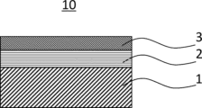
- FIG. 1 is a schematic cross-sectional view schematically showing a reflective mask blank in an embodiment of the present invention.
- FIG. 3 is a schematic cross-sectional view schematically showing a reflective mask blank in another embodiment of the present invention.
- FIG. 3 is a schematic plan view of a hole-like pattern formed in an absorption layer of a reflective mask according to an embodiment of the present invention, in which (a) shows a staggered arrangement and (b) shows an aligned arrangement.
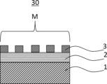
- FIG. 1 is a schematic cross-sectional view schematically showing a reflective mask in an embodiment of the present invention.
- FIG. 3 is a schematic cross-sectional view schematically showing a reflective mask in another embodiment of the present invention.
- FIG. 3 is a schematic diagram for explaining a light intensity distribution in a transfer pattern.
- the terms "on a substrate, on a layer,” and on a film include not only the case where the material is in contact with the upper surface of the film, etc., but also the upper part that is not in contact with the upper surface of the film, etc.
- film B on film A may mean that film A and film B are in contact with each other, or that another film or the like may be interposed between film A and film B.
- above here does not necessarily mean a high position in the vertical direction, but indicates a relative positional relationship.
- the thickness of the formed film, etc. can be measured using a transmission electron microscope or an X-ray reflectance method.
- the preferable numerical range can be determined by arbitrarily combining each of the preferable lower limit and upper limit.
- FIGS. 1 and 2 schematically show cross sections of the reflective mask blank of this embodiment.
- a multilayer reflective film 2 that reflects EUV light and an absorption layer 3 that absorbs EUV light are laminated on a substrate 1 in this order from the substrate 1 side.
- a protective film 4 also called a cap layer
- an antireflection film may be formed on the absorption layer 3 to facilitate pattern defect inspection after mask processing.
- the substrate 1 preferably has a low thermal expansion coefficient at 20°C, preferably 0 ⁇ 0.05 ⁇ 10 -7 /°C, more preferably 0 ⁇ It is 0.03 ⁇ 10 ⁇ 7 /°C. Further, it is preferable that the substrate 1 has excellent smoothness, high flatness, and excellent resistance (chemical resistance) to the cleaning liquid used in the manufacturing process of the reflective mask.
- the material of the substrate 1 include SiO 2 -TiO 2 glass, multi-component glass ceramics, etc., and crystallized glass in which ⁇ -quartz solid solution is precipitated, quartz glass, silicon, metal, etc. can also be used. .
- the substrate 1 is preferably smooth, and has a surface roughness (RMS) of preferably 0.15 nm or less, more preferably 0.10 nm or less. It is. From the same viewpoint, the flatness (TIR; Total Indicated Reading) is preferably 100 nm or less, more preferably 50 nm or less, and still more preferably 30 nm or less.
- RMS surface roughness
- TIR Total Indicated Reading
- the substrate 1 has high rigidity from the viewpoint of preventing deformation due to stress of a film or the like laminated thereon. Specifically, it is preferable that the Young's modulus is 65 GPa or more.
- the multilayer reflective film 2 preferably has a structure in which a plurality of layers containing elements having different refractive indexes as main components are periodically laminated.
- the multilayer reflective film 2 has a structure in which one period is a set of one high refractive index layer and one low refractive index layer, and about 40 to 60 periods are laminated.
- the high refractive index layer/low refractive index layer is generally a Mo/Si multilayer reflective film, but is not limited to this, and includes, for example, a Ru/Si multilayer reflective film, a Mo/Be multilayer reflective film, Mo compound/Si compound multilayer reflective film, Si/Mo/Ru multilayer reflective film, Si/Mo/Ru/Mo multilayer reflective film, MoRu/Si multilayer reflective film, Si/Ru/Mo multilayer reflective film, Si/Ru/Mo /Ru multilayer reflective film, etc. may also be mentioned.
- the multilayer reflective film 2 preferably has a reflectance of 60% or more, more preferably 65% or more of EUV light having a wavelength of around 13.5 nm and incident light at an incident angle of 6°.
- the thickness of each film constituting the multilayer reflective film 2 and the repetition period of lamination are appropriately set according to the film material, desired reflectance of EUV light, and the like.
- the multilayer reflective film 2 can be formed by forming each constituent film to a desired thickness using a known film forming method such as magnetron sputtering or ion beam sputtering.
- a known film forming method such as magnetron sputtering or ion beam sputtering.
- argon (Ar) gas gas pressure 1.3 ⁇ 10 ⁇ 2 to 2.7 ⁇ 10 ⁇ 2 Pa
- a Si film was first deposited to a thickness of 4.5 nm using a Si target, and then a Mo target was deposited.
- a Mo film is formed to a thickness of 2.3 nm using the following method. By repeating this as one cycle and stacking the Mo film/Si film for 30 to 60 cycles, a Mo/Si multilayer reflective film can be formed.
- the reflective mask blank of this embodiment may have a protective film 4 between the multilayer reflective film 2 and the absorption layer 3 to protect the multilayer reflective film 2 from dry etching when forming a mask pattern.
- the protective film 4 also has the role of preventing the multilayer reflective film 2 from being oxidized during EUV exposure and reducing the reflectance of EUV light.
- the etching rate ratio is preferably 10 to 200, more preferably 30 to 100. Note that as the etching gas, a halogen-based gas, an oxygen-based gas, or a mixed gas thereof is usually used.
- halogen-based gas examples include a chlorine-based gas containing one or more selected from Cl 2 , SiCl 4 , CHCl 3 , CCl 4 and BCl 3 ; selected from CF 4 , CHF 3 , SF 6 , BF 3 and XeF 2
- fluorine-based gases examples include fluorine-based gases containing one or more of the following.
- the protective film 4 contains one or more elements selected from, for example, Ru, Rh, and Si.
- the protective film 4 may be a film made only of Rh, but it is also preferable that it contains one or more elements selected from Ru, Nb, Mo, Ta, Ir, Pd, Zr, Y, and Ti.
- one or more elements selected from Ru, Ta, Ir, Pd, and Y are preferred from the viewpoint of improving resistance to etching gas and sulfuric acid peroxide used for cleaning reflective masks.
- one or more elements selected from N, O, C, and B may be included.
- the protective film 4 may be a single layer or a multilayer film consisting of multiple layers.
- the lower layer of the protective film 4 may be formed so as to contact the uppermost surface of the multilayer reflective film 2
- the upper layer of the protective film 4 may be formed so as to contact the lowermost surface of the absorbing layer 3 .
- the protective film 4 may include a layer that does not contain Rh.
- the thickness of the protective film 4 means the total thickness of the multilayer film.
- the thickness of the protective film 4 may be within a range that can sufficiently fulfill the above-mentioned role without interfering with the reflective performance of the multilayer reflective film 2, and is preferably 1.0 to 10.0 nm, more preferably 2.0 nm to 10.0 nm. It is 0 to 3.5 nm. From the same viewpoint, the protective film 4 preferably has a root mean square roughness (RMS) of 0.3 nm or less, more preferably 0.1 nm or less, and is preferably smooth.
- RMS root mean square roughness
- the protective film 4 can be formed by forming a film to a desired thickness using a known film forming method such as DC sputtering, magnetron sputtering, or ion beam sputtering.
- a buffer layer (not shown) may be formed between the protective film 4 and the absorption layer 3 to protect the multilayer reflective film 2 during dry etching or defect correction.
- the material constituting the buffer layer is not particularly limited, and examples thereof include materials containing SiO 2 , Cr, Ta, etc. as main components.
- the absorption layer 3 has a refractive index of less than 0.94 for EUV light with a wavelength of 13.5 nm, and an extinction coefficient of 0.060 or less, and is a multilayer reflective film 2 for the incident light of EUV light with a wavelength of 13.5 nm.
- the phase difference between the light reflected from the surface of the absorption layer 3 and the light reflected from the surface of the absorption layer 3 is 220 to 320°.
- the reflective mask blank of this embodiment is suitable for a reflective mask for EUV lithography that can transfer a fine hole-like pattern with high dimensional accuracy because the absorption layer 3 has such characteristics.
- the refractive index of the absorption layer 3 for EUV light with a wavelength of 13.5 nm is less than 0.94, preferably 0.93 or less, and more preferably 0.92 or less.
- the refractive index is preferably 0.85 or more.
- the extinction coefficient of EUV light with a wavelength of 13.5 nm of the absorption layer 3 is 0.060 or less, preferably 0.010 to 0.050, more preferably 0.020 to 0.045, and even more preferably 0.060. 030 to 0.040.
- phase difference is 220 to 320°, preferably 220 to 280°, more preferably 220 to 260°. Note that the method for measuring the phase difference will be described later. Moreover, the above-mentioned phase difference is a value calculated by an optical multilayer simulation described later. By having a phase difference within the above range, a phase shift mask capable of transferring a fine hole-like pattern with high dimensional accuracy can be obtained.
- the reflected light from the surface of the multilayer reflective film 2 in the phase shift mask passes through the opening of the mask pattern without passing through the absorption layer 3, and passes through the (protective film 4 and) the multilayer reflective film.
- EUV light with a wavelength of 13.5 nm that was directly incident on the multilayer reflective film 2 is reflected by the multilayer reflective film 2 and passed through the opening of the mask pattern without passing through the absorption layer 3 again.
- reflected light from the surface of the absorption layer 3 means that incident light of EUV light with a wavelength of 13.5 nm is transmitted through the absorption layer 3 (and protective film 4) while being absorbed by the absorption layer 3, and the multilayer reflection film 2 This means the reflected light that is reflected by the absorption layer 3 and transmitted through the absorption layer 3 while being absorbed by the absorption layer 3 again.
- the absorption layer of a reflective mask for EUV lithography is desirably thin from the viewpoint of suppressing shadowing, and various constituent materials and structures have been studied. was considered the best.
- the phase difference uses a value calculated by optical multilayer simulation, but can be roughly expressed by the following formula (1).
- ⁇ is the phase difference
- d is the thickness of the absorption layer 3
- ⁇ is the wavelength of the incident light
- n is the refractive index of the absorption layer 3.
- Examples of the mask pattern formed on the absorption layer 3 of the reflective mask blank 10 include a mask pattern including periodically arranged hole-shaped patterns.
- the mask pattern formed on the absorption layer 3 of the reflective mask blank 10 may have a staggered arrangement as shown in FIG. 3(a), or may have an aligned arrangement as shown in FIG. 3(b).
- the width (H1) of the holes H and the interval (H2) between the holes H are both equal, but the width (H1) and the interval (H2) are , the width (H1) and the interval (H2) may be different. Note that in this specification, "width of a hole” means the major axis of the hole.
- EUV lithography is a reduction projection exposure.
- the numerical aperture (NA) of the lens of the exposure device is 0.33
- the reduction ratio of the transferred pattern to the mask pattern is 4 times in the vertical direction (X direction) and 4 times in the horizontal direction (Y direction).
- the dimensions of the hole H are four times the width of the hole in the transfer pattern both vertically (in the X direction) and horizontally (in the Y direction).
- the numerical aperture (NA) of the lens of the exposure device is 0.55
- the reduction ratio of the transferred pattern with respect to the mask pattern is 4 times in the vertical direction (X direction) and 8 times in the horizontal direction (Y direction).
- the length (X direction) of the hole H is four times the hole width of the transfer pattern
- the width (Y direction) is eight times the hole width of the transfer pattern.
- the transfer pattern formed by the hole-like pattern includes a fine hole-like pattern with a hole width of 22 nm or less when the numerical aperture (NA) of the lens of the exposure device is 0.33, for example.
- NA numerical aperture
- the NA 0.55
- the hole width of the transfer pattern is within the above range, more excellent effects as a phase shift mask with high dimensional accuracy can be obtained.
- the material constituting the absorption layer 3 is not particularly limited as long as it can form the phase shift mask as described above, and includes, for example, ruthenium (Ru), rhenium (Re), iridium (Ir), Examples include materials containing osmium (Os) and platinum (Pt).
- the material constituting the absorption layer 3 preferably contains ruthenium (Ru), and further contains tantalum (Ta), tungsten (W), chromium (Cr), molybdenum (Mo), niobium (Nb), and osmium ( It is more preferable that the metal element contains one or more metal elements selected from Os), iridium (Ir), rhenium (Re), and rhodium (Rh).
- the metal elements may be used alone or in combination of two or more.
- the composition ratio of each metal is not particularly limited as long as the refractive index and extinction coefficient of the absorption layer 3 satisfy the above numerical ranges.
- the above-mentioned material may be a single metal element or an alloy, or may be a compound containing, for example, oxygen (O), nitrogen (N), carbon (C), boron (B), hydrogen (H), etc. .
- the ratio of the Ru content [at%] to the Ta content [at%] is preferably 10 to 97, more preferably 15 to 96, more preferably 18 to 95.5, even more preferably 20 to 50. If Ru/Ta is 10 or more, the hydrogen resistance of the phase shift film 13 is likely to be improved, and if it is 97 or less, the etching selectivity is large and the processability of the phase shift film 13 is likely to be good.
- the ratio of the Ru content [at%] to the Cr content [at%] is preferably 1 to 13, more preferably 1 to 6, more preferably 1.5 to 5.7, even more preferably 1.8 to 5.6.
- Ru/Cr is 1 or more, the hydrogen resistance of the phase shift film 13 is easily improved, and when it is 13 or less, the etching selectivity is large and the processability of the phase shift film 13 is likely to be good.
- the ratio of the Ru content [at%] to the W content [at%] is preferably 1 to 20, more preferably 2 to 18, more preferably 2-15, even more preferably 2-9. If Ru/Cr is 1 or more, the hydrogen resistance of the phase shift film 13 is likely to be improved, and if it is 20 or less, the etching selectivity is large and the processability of the phase shift film 13 is likely to be good.
- the total content [at%] of these elements is preferably 1 to 75 at%, more preferably 2 at%. ⁇ 72 at%, more preferably 3 to 50 at%, even more preferably 5 to 30 at%, particularly preferably 7 to 20 at%.
- the absorbent layer 3 may have a multilayer structure in which two or more layers are laminated.
- a multilayer structure is preferable in that the entire absorbent layer 3 can be designed with each layer having a predetermined functional layer made of different materials.
- Functional layers include, for example, a buffer layer that is formed between the reflective layer and the absorbing layer as necessary to prevent damage to the reflective layer during patterning, and a buffer layer that improves the contrast during mask pattern inspection.
- a low reflection layer (a low reflection layer in the wavelength range of the mask pattern inspection light) formed as necessary on the top layer of the absorption layer 3 for the purpose of controlling the reflectance at EUV wavelengths. Examples include a phase control layer formed for the purpose of controlling the phase at EUV wavelength.
- layer combinations in the multilayer structure include Ru/Ta 2 O 5 , Ru/Cr 2 O 3 , Ir/Ta 2 O 5 , Ir/Ru, Pt/Ru, and the like.
- the constituent materials of these layers such as Ru, Ta 2 O 5 , Cr 2 O 3 , Ir, Pt, etc. may be alloys, nitrogen substances, acid It may also be a nitride, a boride, or the like.
- the lamination order may be any order; for example, in the case of the above-mentioned two-layer structure, the order is preferably first layer/second layer.
- the refractive index and extinction coefficient are obtained as a weighted average value taking into account the thickness of each layer.
- the absorption layer 3 can be formed by forming each constituent film to a desired thickness using a known film forming method such as magnetron sputtering or ion beam sputtering.
- the total thickness of the absorption layer 3 is 60 nm or less, and it can exhibit the effect as a phase shift mask that can transfer a fine hole-like pattern with high dimensional accuracy while suppressing shadowing.
- the total thickness of the absorption layer 3 is preferably thin from the viewpoint of etching efficiency during film formation of the absorption layer 3 and mask pattern formation, and is preferably 60 nm or less, more preferably 58 nm or less, and even more preferably 53 nm or less. It is. Further, the total thickness of the absorption layer 3 is preferably 20 nm or more from the viewpoint of the absorption effect of EUV light.
- An antireflection film (not shown) may be laminated on the absorption layer 3 to prevent reflection when DUV light (deep ultraviolet light) with a wavelength of 190 to 260 nm is used in the inspection process.
- the reflective mask is sometimes inspected for defects in the mask pattern formed on the absorption layer 3.
- the presence or absence of defects is determined mainly based on the optical data of the reflected light of the inspection light. Therefore, the light that passes through the mask cannot be used as the inspection light, and DUV light is used. For this reason, when the above-mentioned mask inspection is performed, it is preferable to provide an antireflection film on the absorption layer 3 to prevent reflection of DUV light, which is the inspection light, for accurate inspection.
- the antireflection film is preferably formed of a material that has a lower refractive index for DUV light than the absorption layer 3.
- the constituent material of the antireflection film include a material containing Ta as a main component and one or more components selected from Hf, Ge, Si, B, N, H, and O in addition to Ta. Specific examples include TaO, TaON, TaONH, TaHfO, TaHfON, TaBSiO, TaBSiON, and the like.
- the antireflection film can be formed by forming a film to a desired thickness using, for example, a known film forming method such as magnetron sputtering or ion beam sputtering.
- the reflective mask blank of this embodiment may be provided with a known functional film for reflective mask blanks.
- a back conductive film may be formed on the surface (back surface) opposite to the multilayer reflective film 2 of the substrate 1. good.
- the back conductive film preferably has a sheet resistance of 100 ⁇ / ⁇ or less, and a known configuration can be applied.
- the constituent material of the back conductive film include Si, TiN, Mo, Cr, TaSi, and the like.
- the thickness of the back conductive film can be, for example, 10 to 1000 nm.
- the back conductive film is formed to a desired thickness using a known film forming method such as magnetron sputtering, ion beam sputtering, chemical vapor deposition (CVD), vacuum evaporation, or electroplating. It can be formed by coating.
- a known film forming method such as magnetron sputtering, ion beam sputtering, chemical vapor deposition (CVD), vacuum evaporation, or electroplating. It can be formed by coating.
- the reflective mask blank of the present invention has a reflectance of EUV light of preferably 2.0 to 30%, more preferably 3.0 to 25%, still more preferably 5.0 to 20%, even more preferably 6. .0 to 15.0%, particularly preferably 8.0 to 10%.
- the reflective mask 30 shown in FIG. 4 is a reflective mask for EUV lithography in which a multilayer reflective film 2 that reflects EUV light and an absorption layer 3 that absorbs EUV light are laminated in this order from the substrate 1 side on a substrate 1. type mask, the absorption layer 3 has a refractive index of less than 0.94 for EUV light with a wavelength of 13.5 nm, an extinction coefficient of 0.060 or less, and absorbs incident light of EUV light with a wavelength of 13.5 nm.
- the phase difference between the light reflected from the surface of the multilayer reflective film 2 and the light reflected from the surface of the absorption layer 3 is 220 to 320°, preferably 220 to 280°, and the absorption layer 3 has a mask pattern M. It is being formed. As shown in FIG. 5, a protective film 4 may be formed between the multilayer reflective film 2 and the absorption layer 3 to protect the multilayer reflective film 2 from dry etching when forming a mask pattern.
- the reflective mask of the present invention has a mask pattern M formed on the absorption layer 3 of the reflective mask blank 10 of the present embodiment. Therefore, the description of each constituent layer of the reflective mask 30 is the same as that of the reflective mask blank 10 described above, and will therefore be omitted.
- the mask pattern M preferably includes a periodically arranged hole pattern from the viewpoint of supporting a more complex semiconductor circuit.
- the reflective mask 30 has a normalized image log slope (NILS) of the hole-like pattern, preferably 1.4 or more, more preferably 1.5 or more, More preferably, it is 2.0 or more.
- NILS normalized image log slope
- the reflective mask 30 has holes in the transfer pattern formed by the hole-like pattern, for example, if the numerical aperture (NA) of the lens of the exposure device is 0.33, It is suitable when the material includes a fine hole-like pattern with a width of 22 nm or less, and when NA is 0.55, it is suitable when the material contains a fine hole-like pattern with a hole width of 14 nm or less. When the hole width is within the above range, a more excellent effect as a phase shift mask with high dimensional accuracy can be obtained.
- NA numerical aperture
- the present invention provides high dimensional accuracy when the phase difference between the light reflected from the multilayer reflective film and the light reflected from the absorption layer is larger than before in the absorbing layer in a mask including a fine hole-like pattern in EUV lithography. This is based on the discovery that it is possible to form a transfer pattern using Further, the present inventor focused on the refractive index n, extinction coefficient k, and phase difference of the absorption layer 3 for EUV light, and found that there is a range in which high transfer accuracy can be achieved in an EUV mask including a hole-like pattern. I found out.
- the excellent transfer accuracy by the reflective mask 30 can be estimated from the normalized image log slope (NILS).
- NILS is a characteristic value indicating the contrast between bright and dark areas of light intensity in a transferred pattern. It can be said that the higher the value of NILS, the higher the contrast of the transferred pattern and the better the transfer accuracy.
- NILS is determined by the following formula (2).
- I(x) is the light intensity distribution in the transfer pattern (intensity normalized by the maximum intensity, dimensionless quantity), and x is the distance from the peak position in the hole width direction of the transfer pattern (unit: nm) ), CD represents the critical dimension of the hole width at the resolution limit of the transfer pattern. Note that in this specification, CD corresponds to the hole width of the transfer pattern.
- FIG. 6 shows an outline of the light intensity distribution I(x).
- NILS is the slope of lnI(x) (natural logarithm of I(x)) when the width (x 2 - x 1 ) at the peak of I(x) is equal to CD, as shown in FIG. It is obtained as the product of CD.
- I(x) is based on known optical imaging theory (for example, Koichi Matsumoto, "Lithography Optics”, “Optics”, Optical Society of Japan, March 2001, Vol. 30, No. 3, p. 40-47) (Reference) is determined by lithography simulation.
- optical imaging theory for example, Koichi Matsumoto, "Lithography Optics”, “Optics”, Optical Society of Japan, March 2001, Vol. 30, No. 3, p. 40-47
- Reference is determined by lithography simulation.
- commercially available software for example, lithography simulator "PROLITH”, manufactured by KLA-Tencor; "Sentaurus Lithography”, manufactured by Synopsis, etc.
- simulations were performed assuming that the numerical aperture NA of the lens of the EUV exposure apparatus was 0.33, or 0.55 in consideration of a next-generation model aimed at further miniaturization of patterns.
- the refractive index n is 0.88 to 0.96
- the extinction coefficient k is 0.015 to 0.065
- the absorption layer thickness d Calculations were performed repeatedly while changing the value in the range of 20 to 80 nm, and d (optimal value) at which the NILS was maximized was determined at predetermined n and k. Furthermore, the optimum value of the phase difference was determined from the values of d, n, and k at this time.
- each alloy is Ru 0.7 Cr 0.3 , Ru 0.7 Ta 0.3 , Ru 0.5 W 0 It was set as .5 . Strictly speaking, the optical constants of each alloy may vary slightly depending on the density and film forming conditions, so representative values were used. Further, the first layer and the second layer in Table 2 mean that they are formed in this order from the substrate 1 side.
- the NILS is high and the contrast of the transferred pattern is high.
- the phase difference between the light reflected from the surface of the multilayer reflective film 2 and the light reflected from the surface of the absorption layer 3 is 220 to 320 degrees, and even if the total thickness is 60 nm or less, the dimensional accuracy is It can be said that a transfer pattern with high quality can be obtained.
- n is, the more preferable it is, for example, a suitable range is n less than 0.94, more preferably 0.93 or less, still more preferably 0.92 or less.
- the extinction coefficient k has a smaller influence than the refractive index n, it can be seen that the NILS increases in a region where k is low.
- a suitable range is for k to be 0.06 or less, more preferably 0.05 or less, still more preferably 0.04 or less. It can be seen that the phase difference at this time varies depending on the refractive index n and extinction coefficient k of the material, but falls within the range of 220 to 230°. Similarly, in FIGS.
- the extinction coefficient k has a smaller effect than the refractive index n, but from the viewpoint of compatibility with various CDs, the preferred range is similarly that k is 0.06 or less, and It is preferably 0.05 or less, more preferably 0.04 or less.
- the phase difference at this time varies depending on the refractive index n and extinction coefficient k of the material, but is 230 to 270°, and it can be seen that the narrower the CD, the higher the optimal phase difference.
- phase difference that takes the maximum value of NILS increases when the CD becomes narrower is considered as follows.
- a phase shift mask provides a reversal phase difference to light transmitted through the transparent portions of the mask pattern by making the transparent portions of a different material or shape from the adjacent transparent portions.
- the electric field of light changes continuously at the interface between a transparent part on the mask pattern and an adjacent transparent part.
- the period of the unevenness of the EUV mask pattern becomes smaller. Therefore, the electric field of light inside the pattern structure of the EUV mask is bent significantly in a shorter period than when the CD is large.
- the CD of the EUV mask structure when it is made narrower than when it is sufficiently large compared to the wavelength, the contribution of electric field distortion inside the concavo-convex pattern increases, and as a result, the transmission part of the mask pattern and It is thought that a phenomenon occurs in which the average phase difference between adjacent transparent parts becomes smaller than the intended value (that is, the value calculated by the above simulation or the above equation (1)). Therefore, if the CD is narrow, the thickness of the mask is adjusted in advance to create a mask that can provide a larger phase difference than the conventional one as calculated by the above simulation or the above formula (1). By doing so, it becomes possible to realize the effect of a phase shift mask.
- FIG. 3 is a diagram showing a distribution of phase difference values. It can be seen from FIG. 8 that as the CD becomes narrower, the thickness of the absorption layer that takes the maximum value of NILS becomes thicker, and the optimum value of the phase difference corresponding to this becomes higher.
- Table 4 is organized by film thickness when NILS in the 4x direction is maximum.
- the reason why the NILS in the 4x direction was selected as a reference is because the concavo-convex period of the EUV mask pattern is smaller than that in the 8x direction, so that the contribution of the distortion of the electric field inside the above-mentioned concavo-convex pattern becomes larger.
- the irregularity period of the EUV mask pattern is smaller in the 4x direction than in the 8x direction, making it difficult to process. It is desirable to do so.
- the NILS may be high and the contrast of the transferred pattern may be high.
- the phase difference between the light reflected from the surface of the multilayer reflective film 2 and the light reflected from the surface of the absorption layer 3 is 220 to 320 degrees, and even if the total thickness is 60 nm or less, the dimensional accuracy is It can be said that a transfer pattern with high quality can be obtained.
- the reflective mask 30 can be manufactured by forming a mask pattern M using the reflective mask blank 10 by applying a known lithography technique. For example, a photoresist film is formed on the absorption layer 3 of the reflective mask blank 10, processed into a resist pattern having a desired pattern shape, and after etching the absorption layer 3 by dry etching or the like, the resist pattern is By removing unnecessary photoresist including , a reflective mask 30 in which a mask pattern M is formed on the absorption layer 3 can be obtained.
- the part of the absorption layer 3 from which the photoresist has been removed is the transmission part, and the part of the absorption layer 3 from which the photoresist has not been removed is the area between the two transmission parts.
- a mask pattern M is configured.
- Substrate 2 Multilayer reflective film 3
- Absorption layer 4 Protective film 10, 20 Reflective mask blank 30, 40
- Reflective mask H Hole-shaped hole H1 Width of hole H2 Spacing between holes X Vertical (X direction) Y horizontal (Y direction) M mask pattern
Landscapes
- Physics & Mathematics (AREA)
- General Physics & Mathematics (AREA)
- Preparing Plates And Mask In Photomechanical Process (AREA)
- Exposure Of Semiconductors, Excluding Electron Or Ion Beam Exposure (AREA)
Priority Applications (3)
| Application Number | Priority Date | Filing Date | Title |
|---|---|---|---|
| JP2024539094A JPWO2024029410A1 (https=) | 2022-08-03 | 2023-07-25 | |
| KR1020257002973A KR20250047993A (ko) | 2022-08-03 | 2023-07-25 | 반사형 마스크 블랭크 및 반사형 마스크 |
| US19/026,266 US20250172864A1 (en) | 2022-08-03 | 2025-01-16 | Reflective mask blank and reflective mask |
Applications Claiming Priority (2)
| Application Number | Priority Date | Filing Date | Title |
|---|---|---|---|
| JP2022124355 | 2022-08-03 | ||
| JP2022-124355 | 2022-08-03 |
Related Child Applications (1)
| Application Number | Title | Priority Date | Filing Date |
|---|---|---|---|
| US19/026,266 Continuation US20250172864A1 (en) | 2022-08-03 | 2025-01-16 | Reflective mask blank and reflective mask |
Publications (1)
| Publication Number | Publication Date |
|---|---|
| WO2024029410A1 true WO2024029410A1 (ja) | 2024-02-08 |
Family
ID=89849013
Family Applications (1)
| Application Number | Title | Priority Date | Filing Date |
|---|---|---|---|
| PCT/JP2023/027272 Ceased WO2024029410A1 (ja) | 2022-08-03 | 2023-07-25 | 反射型マスクブランク及び反射型マスク |
Country Status (5)
| Country | Link |
|---|---|
| US (1) | US20250172864A1 (https=) |
| JP (1) | JPWO2024029410A1 (https=) |
| KR (1) | KR20250047993A (https=) |
| TW (1) | TW202409710A (https=) |
| WO (1) | WO2024029410A1 (https=) |
Cited By (2)
| Publication number | Priority date | Publication date | Assignee | Title |
|---|---|---|---|---|
| JP7681153B1 (ja) | 2024-04-11 | 2025-05-21 | テクセンドフォトマスク株式会社 | 反射型フォトマスクブランク、反射型フォトマスク及び反射型フォトマスクの製造方法 |
| WO2025239179A1 (ja) * | 2024-05-13 | 2025-11-20 | Agc株式会社 | 反射型マスクブランク、反射型マスク、反射型マスクの製造方法 |
Citations (6)
| Publication number | Priority date | Publication date | Assignee | Title |
|---|---|---|---|---|
| WO2019225736A1 (ja) * | 2018-05-25 | 2019-11-28 | Hoya株式会社 | 反射型マスクブランク、反射型マスク及びその製造方法、並びに半導体装置の製造方法 |
| WO2021132111A1 (ja) * | 2019-12-27 | 2021-07-01 | Agc株式会社 | Euvリソグラフィ用反射型マスクブランク、euvリソグラフィ用反射型マスク、およびそれらの製造方法 |
| JP6929983B1 (ja) * | 2020-03-10 | 2021-09-01 | Hoya株式会社 | 反射型マスクブランクおよび反射型マスク、並びに半導体デバイスの製造方法 |
| JP2022024617A (ja) * | 2020-07-28 | 2022-02-09 | Agc株式会社 | Euvリソグラフィ用反射型マスクブランク、euvリソグラフィ用反射型マスク、およびそれらの製造方法 |
| WO2022050156A1 (ja) * | 2020-09-04 | 2022-03-10 | Agc株式会社 | 反射型マスク、反射型マスクブランク、および反射型マスクの製造方法 |
| WO2022065144A1 (ja) * | 2020-09-28 | 2022-03-31 | Hoya株式会社 | 多層反射膜付き基板、反射型マスクブランク、反射型マスクの製造方法、及び半導体装置の製造方法 |
Family Cites Families (1)
| Publication number | Priority date | Publication date | Assignee | Title |
|---|---|---|---|---|
| JP5766393B2 (ja) | 2009-07-23 | 2015-08-19 | 株式会社東芝 | 反射型露光用マスクおよび半導体装置の製造方法 |
-
2023
- 2023-07-25 JP JP2024539094A patent/JPWO2024029410A1/ja active Pending
- 2023-07-25 KR KR1020257002973A patent/KR20250047993A/ko active Pending
- 2023-07-25 WO PCT/JP2023/027272 patent/WO2024029410A1/ja not_active Ceased
- 2023-07-28 TW TW112128451A patent/TW202409710A/zh unknown
-
2025
- 2025-01-16 US US19/026,266 patent/US20250172864A1/en active Pending
Patent Citations (6)
| Publication number | Priority date | Publication date | Assignee | Title |
|---|---|---|---|---|
| WO2019225736A1 (ja) * | 2018-05-25 | 2019-11-28 | Hoya株式会社 | 反射型マスクブランク、反射型マスク及びその製造方法、並びに半導体装置の製造方法 |
| WO2021132111A1 (ja) * | 2019-12-27 | 2021-07-01 | Agc株式会社 | Euvリソグラフィ用反射型マスクブランク、euvリソグラフィ用反射型マスク、およびそれらの製造方法 |
| JP6929983B1 (ja) * | 2020-03-10 | 2021-09-01 | Hoya株式会社 | 反射型マスクブランクおよび反射型マスク、並びに半導体デバイスの製造方法 |
| JP2022024617A (ja) * | 2020-07-28 | 2022-02-09 | Agc株式会社 | Euvリソグラフィ用反射型マスクブランク、euvリソグラフィ用反射型マスク、およびそれらの製造方法 |
| WO2022050156A1 (ja) * | 2020-09-04 | 2022-03-10 | Agc株式会社 | 反射型マスク、反射型マスクブランク、および反射型マスクの製造方法 |
| WO2022065144A1 (ja) * | 2020-09-28 | 2022-03-31 | Hoya株式会社 | 多層反射膜付き基板、反射型マスクブランク、反射型マスクの製造方法、及び半導体装置の製造方法 |
Cited By (4)
| Publication number | Priority date | Publication date | Assignee | Title |
|---|---|---|---|---|
| JP7681153B1 (ja) | 2024-04-11 | 2025-05-21 | テクセンドフォトマスク株式会社 | 反射型フォトマスクブランク、反射型フォトマスク及び反射型フォトマスクの製造方法 |
| WO2025216119A1 (ja) * | 2024-04-11 | 2025-10-16 | テクセンドフォトマスク株式会社 | 反射型フォトマスクブランク、反射型フォトマスク及び反射型フォトマスクの製造方法 |
| JP2025161069A (ja) * | 2024-04-11 | 2025-10-24 | テクセンドフォトマスク株式会社 | 反射型フォトマスクブランク、反射型フォトマスク及び反射型フォトマスクの製造方法 |
| WO2025239179A1 (ja) * | 2024-05-13 | 2025-11-20 | Agc株式会社 | 反射型マスクブランク、反射型マスク、反射型マスクの製造方法 |
Also Published As
| Publication number | Publication date |
|---|---|
| KR20250047993A (ko) | 2025-04-07 |
| TW202409710A (zh) | 2024-03-01 |
| JPWO2024029410A1 (https=) | 2024-02-08 |
| US20250172864A1 (en) | 2025-05-29 |
Similar Documents
| Publication | Publication Date | Title |
|---|---|---|
| JP7047046B2 (ja) | マスクブランク用基板、多層反射膜付き基板、反射型マスクブランク及び反射型マスク、並びに半導体装置の製造方法 | |
| KR102802783B1 (ko) | 반사형 마스크 블랭크, 반사형 마스크 및 반사형 마스크 블랭크의 제조 방법 | |
| TWI881058B (zh) | 反射型光罩基底及反射型光罩、與半導體裝置之製造方法 | |
| JP6636581B2 (ja) | 反射型マスクブランク、反射型マスクの製造方法、及び半導体装置の製造方法 | |
| KR102938891B1 (ko) | 반사형 마스크 블랭크 및 반사형 마스크, 그리고 반도체 장치의 제조 방법 | |
| JP5590044B2 (ja) | Euvリソグラフィ用光学部材 | |
| JPWO2019225737A1 (ja) | 反射型マスクブランク、反射型マスク、並びに反射型マスク及び半導体装置の製造方法 | |
| JPWO2019225736A1 (ja) | 反射型マスクブランク、反射型マスク及びその製造方法、並びに半導体装置の製造方法 | |
| KR102002441B1 (ko) | 반사형 마스크 블랭크, 반사형 마스크 및 그 제조 방법, 및 반도체 장치의 제조 방법 | |
| KR20190059326A (ko) | 반사형 마스크 블랭크, 반사형 마스크의 제조 방법, 및 반도체 장치의 제조 방법 | |
| KR20160034315A (ko) | 다층 반사막을 구비한 기판, euv 리소그래피용 반사형 마스크 블랭크, euv 리소그래피용 반사형 마스크 및 그 제조 방법과 반도체 장치의 제조 방법 | |
| WO2020184473A1 (ja) | 反射型マスクブランク、反射型マスク及びその製造方法、並びに半導体装置の製造方法 | |
| US20250172864A1 (en) | Reflective mask blank and reflective mask | |
| JP6441012B2 (ja) | 反射型マスクブランク、反射型マスク及びその製造方法、並びに半導体装置の製造方法 | |
| KR20160054458A (ko) | 다층 반사막을 구비한 기판, euv 리소그래피용 반사형 마스크 블랭크, euv 리소그래피용 반사형 마스크 및 그 제조 방법과 반도체 장치의 제조 방법 | |
| WO2021193089A1 (ja) | 多層反射膜付き基板、反射型マスクブランク、反射型マスク、及び半導体デバイスの製造方法 | |
| TW202219625A (zh) | 附多層反射膜之基板、反射型光罩基底、反射型光罩之製造方法及半導體裝置之製造方法 | |
| WO2023008435A1 (ja) | 反射型マスクブランク、反射型マスク、反射型マスクブランクの製造方法、及び反射型マスクの製造方法 | |
| WO2024029409A1 (ja) | 反射型マスクブランク及び反射型マスク | |
| WO2023171582A1 (ja) | 反射型マスクブランク、並びに、反射型マスク及びその製造方法 |
Legal Events
| Date | Code | Title | Description |
|---|---|---|---|
| 121 | Ep: the epo has been informed by wipo that ep was designated in this application |
Ref document number: 23849965 Country of ref document: EP Kind code of ref document: A1 |
|
| WWE | Wipo information: entry into national phase |
Ref document number: 2024539094 Country of ref document: JP |
|
| NENP | Non-entry into the national phase |
Ref country code: DE |
|
| WWE | Wipo information: entry into national phase |
Ref document number: 11202500497P Country of ref document: SG |
|
| WWP | Wipo information: published in national office |
Ref document number: 11202500497P Country of ref document: SG |
|
| WWP | Wipo information: published in national office |
Ref document number: 1020257002973 Country of ref document: KR |
|
| 122 | Ep: pct application non-entry in european phase |
Ref document number: 23849965 Country of ref document: EP Kind code of ref document: A1 |