WO2024029410A1 - Reflective mask blank and reflective mask - Google Patents
Reflective mask blank and reflective mask Download PDFInfo
- Publication number
- WO2024029410A1 WO2024029410A1 PCT/JP2023/027272 JP2023027272W WO2024029410A1 WO 2024029410 A1 WO2024029410 A1 WO 2024029410A1 JP 2023027272 W JP2023027272 W JP 2023027272W WO 2024029410 A1 WO2024029410 A1 WO 2024029410A1
- Authority
- WO
- WIPO (PCT)
- Prior art keywords
- absorption layer
- reflective mask
- less
- pattern
- film
- Prior art date
Links
- 238000010521 absorption reaction Methods 0.000 claims abstract description 115
- 238000012546 transfer Methods 0.000 claims abstract description 38
- 230000008033 biological extinction Effects 0.000 claims abstract description 36
- 239000000758 substrate Substances 0.000 claims abstract description 25
- 238000001900 extreme ultraviolet lithography Methods 0.000 claims abstract description 18
- 230000001681 protective effect Effects 0.000 claims description 30
- 239000011651 chromium Substances 0.000 claims description 16
- 229910052751 metal Inorganic materials 0.000 claims description 11
- 239000010948 rhodium Substances 0.000 claims description 11
- 229910052741 iridium Inorganic materials 0.000 claims description 7
- 239000010955 niobium Substances 0.000 claims description 6
- 229910052707 ruthenium Inorganic materials 0.000 claims description 6
- 229910052804 chromium Inorganic materials 0.000 claims description 5
- 229910052750 molybdenum Inorganic materials 0.000 claims description 5
- 229910052715 tantalum Inorganic materials 0.000 claims description 5
- KJTLSVCANCCWHF-UHFFFAOYSA-N Ruthenium Chemical compound [Ru] KJTLSVCANCCWHF-UHFFFAOYSA-N 0.000 claims description 4
- GKOZUEZYRPOHIO-UHFFFAOYSA-N iridium atom Chemical compound [Ir] GKOZUEZYRPOHIO-UHFFFAOYSA-N 0.000 claims description 4
- 229910052762 osmium Inorganic materials 0.000 claims description 4
- SYQBFIAQOQZEGI-UHFFFAOYSA-N osmium atom Chemical compound [Os] SYQBFIAQOQZEGI-UHFFFAOYSA-N 0.000 claims description 4
- 229910052702 rhenium Inorganic materials 0.000 claims description 4
- WUAPFZMCVAUBPE-UHFFFAOYSA-N rhenium atom Chemical compound [Re] WUAPFZMCVAUBPE-UHFFFAOYSA-N 0.000 claims description 4
- 229910052703 rhodium Inorganic materials 0.000 claims description 4
- VYZAMTAEIAYCRO-UHFFFAOYSA-N Chromium Chemical compound [Cr] VYZAMTAEIAYCRO-UHFFFAOYSA-N 0.000 claims description 3
- ZOKXTWBITQBERF-UHFFFAOYSA-N Molybdenum Chemical compound [Mo] ZOKXTWBITQBERF-UHFFFAOYSA-N 0.000 claims description 3
- 239000011733 molybdenum Substances 0.000 claims description 3
- 229910052758 niobium Inorganic materials 0.000 claims description 3
- GUCVJGMIXFAOAE-UHFFFAOYSA-N niobium atom Chemical compound [Nb] GUCVJGMIXFAOAE-UHFFFAOYSA-N 0.000 claims description 3
- MHOVAHRLVXNVSD-UHFFFAOYSA-N rhodium atom Chemical compound [Rh] MHOVAHRLVXNVSD-UHFFFAOYSA-N 0.000 claims description 3
- GUVRBAGPIYLISA-UHFFFAOYSA-N tantalum atom Chemical compound [Ta] GUVRBAGPIYLISA-UHFFFAOYSA-N 0.000 claims description 3
- WFKWXMTUELFFGS-UHFFFAOYSA-N tungsten Chemical compound [W] WFKWXMTUELFFGS-UHFFFAOYSA-N 0.000 claims description 3
- 229910052721 tungsten Inorganic materials 0.000 claims description 3
- 239000010937 tungsten Substances 0.000 claims description 3
- 238000010030 laminating Methods 0.000 claims description 2
- 239000010410 layer Substances 0.000 description 149
- 239000010408 film Substances 0.000 description 147
- 239000000463 material Substances 0.000 description 27
- 230000010363 phase shift Effects 0.000 description 26
- 238000004088 simulation Methods 0.000 description 18
- 238000009826 distribution Methods 0.000 description 13
- 238000005530 etching Methods 0.000 description 12
- 239000007789 gas Substances 0.000 description 12
- 238000000034 method Methods 0.000 description 12
- 239000000470 constituent Substances 0.000 description 11
- 238000010586 diagram Methods 0.000 description 10
- 238000007689 inspection Methods 0.000 description 10
- 230000000694 effects Effects 0.000 description 9
- 229910045601 alloy Inorganic materials 0.000 description 8
- 239000000956 alloy Substances 0.000 description 8
- 230000005540 biological transmission Effects 0.000 description 8
- 230000003287 optical effect Effects 0.000 description 8
- 238000001312 dry etching Methods 0.000 description 6
- 229910052739 hydrogen Inorganic materials 0.000 description 6
- 238000001659 ion-beam spectroscopy Methods 0.000 description 6
- 239000002184 metal Substances 0.000 description 6
- 238000001459 lithography Methods 0.000 description 5
- 238000001755 magnetron sputter deposition Methods 0.000 description 5
- 229910052760 oxygen Inorganic materials 0.000 description 5
- BASFCYQUMIYNBI-UHFFFAOYSA-N platinum Chemical compound [Pt] BASFCYQUMIYNBI-UHFFFAOYSA-N 0.000 description 5
- IJGRMHOSHXDMSA-UHFFFAOYSA-N Atomic nitrogen Chemical compound N#N IJGRMHOSHXDMSA-UHFFFAOYSA-N 0.000 description 4
- UFHFLCQGNIYNRP-UHFFFAOYSA-N Hydrogen Chemical compound [H][H] UFHFLCQGNIYNRP-UHFFFAOYSA-N 0.000 description 4
- 229910052796 boron Inorganic materials 0.000 description 4
- 230000007547 defect Effects 0.000 description 4
- 230000005684 electric field Effects 0.000 description 4
- 239000001257 hydrogen Substances 0.000 description 4
- 238000005286 illumination Methods 0.000 description 4
- 229910052757 nitrogen Inorganic materials 0.000 description 4
- 229920002120 photoresistant polymer Polymers 0.000 description 4
- 238000012545 processing Methods 0.000 description 4
- 230000002745 absorbent Effects 0.000 description 3
- 239000002250 absorbent Substances 0.000 description 3
- 229910052799 carbon Inorganic materials 0.000 description 3
- 150000001875 compounds Chemical class 0.000 description 3
- 239000000203 mixture Substances 0.000 description 3
- 229910052697 platinum Inorganic materials 0.000 description 3
- 239000004065 semiconductor Substances 0.000 description 3
- 229910052710 silicon Inorganic materials 0.000 description 3
- 238000002834 transmittance Methods 0.000 description 3
- XKRFYHLGVUSROY-UHFFFAOYSA-N Argon Chemical compound [Ar] XKRFYHLGVUSROY-UHFFFAOYSA-N 0.000 description 2
- 229910004298 SiO 2 Inorganic materials 0.000 description 2
- QVGXLLKOCUKJST-UHFFFAOYSA-N atomic oxygen Chemical compound [O] QVGXLLKOCUKJST-UHFFFAOYSA-N 0.000 description 2
- 238000005229 chemical vapour deposition Methods 0.000 description 2
- 239000000460 chlorine Substances 0.000 description 2
- 238000004140 cleaning Methods 0.000 description 2
- 238000005516 engineering process Methods 0.000 description 2
- 239000011521 glass Substances 0.000 description 2
- 229910052736 halogen Inorganic materials 0.000 description 2
- 150000002367 halogens Chemical class 0.000 description 2
- 238000003475 lamination Methods 0.000 description 2
- 239000002346 layers by function Substances 0.000 description 2
- 238000004519 manufacturing process Methods 0.000 description 2
- 238000013041 optical simulation Methods 0.000 description 2
- 239000001301 oxygen Substances 0.000 description 2
- 229910052763 palladium Inorganic materials 0.000 description 2
- 238000004544 sputter deposition Methods 0.000 description 2
- 239000000126 substance Substances 0.000 description 2
- 229910052727 yttrium Inorganic materials 0.000 description 2
- 229910000952 Be alloy Inorganic materials 0.000 description 1
- ZOXJGFHDIHLPTG-UHFFFAOYSA-N Boron Chemical compound [B] ZOXJGFHDIHLPTG-UHFFFAOYSA-N 0.000 description 1
- OKTJSMMVPCPJKN-UHFFFAOYSA-N Carbon Chemical compound [C] OKTJSMMVPCPJKN-UHFFFAOYSA-N 0.000 description 1
- ZAMOUSCENKQFHK-UHFFFAOYSA-N Chlorine atom Chemical compound [Cl] ZAMOUSCENKQFHK-UHFFFAOYSA-N 0.000 description 1
- YCKRFDGAMUMZLT-UHFFFAOYSA-N Fluorine atom Chemical compound [F] YCKRFDGAMUMZLT-UHFFFAOYSA-N 0.000 description 1
- 229910015799 MoRu Inorganic materials 0.000 description 1
- 241000917012 Quercus floribunda Species 0.000 description 1
- 235000003976 Ruta Nutrition 0.000 description 1
- 240000005746 Ruta graveolens Species 0.000 description 1
- 229910003902 SiCl 4 Inorganic materials 0.000 description 1
- VYPSYNLAJGMNEJ-UHFFFAOYSA-N Silicium dioxide Chemical compound O=[Si]=O VYPSYNLAJGMNEJ-UHFFFAOYSA-N 0.000 description 1
- 229910003071 TaON Inorganic materials 0.000 description 1
- 229910010413 TiO 2 Inorganic materials 0.000 description 1
- ATJFFYVFTNAWJD-UHFFFAOYSA-N Tin Chemical compound [Sn] ATJFFYVFTNAWJD-UHFFFAOYSA-N 0.000 description 1
- 239000002253 acid Substances 0.000 description 1
- 229910052786 argon Inorganic materials 0.000 description 1
- 230000015572 biosynthetic process Effects 0.000 description 1
- 238000004364 calculation method Methods 0.000 description 1
- 239000003990 capacitor Substances 0.000 description 1
- 229910052801 chlorine Inorganic materials 0.000 description 1
- 239000011248 coating agent Substances 0.000 description 1
- 238000000576 coating method Methods 0.000 description 1
- 238000012937 correction Methods 0.000 description 1
- 230000007423 decrease Effects 0.000 description 1
- 238000000151 deposition Methods 0.000 description 1
- 230000008021 deposition Effects 0.000 description 1
- 238000011161 development Methods 0.000 description 1
- 230000018109 developmental process Effects 0.000 description 1
- 238000009713 electroplating Methods 0.000 description 1
- 229910052731 fluorine Inorganic materials 0.000 description 1
- 239000011737 fluorine Substances 0.000 description 1
- 229910052732 germanium Inorganic materials 0.000 description 1
- 239000002241 glass-ceramic Substances 0.000 description 1
- 229910052735 hafnium Inorganic materials 0.000 description 1
- 230000010354 integration Effects 0.000 description 1
- 230000002452 interceptive effect Effects 0.000 description 1
- 239000007788 liquid Substances 0.000 description 1
- 150000004767 nitrides Chemical class 0.000 description 1
- 238000012634 optical imaging Methods 0.000 description 1
- 238000000059 patterning Methods 0.000 description 1
- 230000007261 regionalization Effects 0.000 description 1
- 235000005806 ruta Nutrition 0.000 description 1
- 239000010703 silicon Substances 0.000 description 1
- 239000002356 single layer Substances 0.000 description 1
- QAOWNCQODCNURD-UHFFFAOYSA-N sulfuric acid Substances OS(O)(=O)=O QAOWNCQODCNURD-UHFFFAOYSA-N 0.000 description 1
- -1 sulfuric acid peroxide Chemical class 0.000 description 1
- 230000003746 surface roughness Effects 0.000 description 1
- 239000010409 thin film Substances 0.000 description 1
- 229910052718 tin Inorganic materials 0.000 description 1
- 229910052719 titanium Inorganic materials 0.000 description 1
- 238000007738 vacuum evaporation Methods 0.000 description 1
- 229910052726 zirconium Inorganic materials 0.000 description 1
- 229910000500 β-quartz Inorganic materials 0.000 description 1
Images


Classifications
-
- G—PHYSICS
- G03—PHOTOGRAPHY; CINEMATOGRAPHY; ANALOGOUS TECHNIQUES USING WAVES OTHER THAN OPTICAL WAVES; ELECTROGRAPHY; HOLOGRAPHY
- G03F—PHOTOMECHANICAL PRODUCTION OF TEXTURED OR PATTERNED SURFACES, e.g. FOR PRINTING, FOR PROCESSING OF SEMICONDUCTOR DEVICES; MATERIALS THEREFOR; ORIGINALS THEREFOR; APPARATUS SPECIALLY ADAPTED THEREFOR
- G03F1/00—Originals for photomechanical production of textured or patterned surfaces, e.g., masks, photo-masks, reticles; Mask blanks or pellicles therefor; Containers specially adapted therefor; Preparation thereof
- G03F1/22—Masks or mask blanks for imaging by radiation of 100nm or shorter wavelength, e.g. X-ray masks, extreme ultraviolet [EUV] masks; Preparation thereof
- G03F1/24—Reflection masks; Preparation thereof
-
- G—PHYSICS
- G03—PHOTOGRAPHY; CINEMATOGRAPHY; ANALOGOUS TECHNIQUES USING WAVES OTHER THAN OPTICAL WAVES; ELECTROGRAPHY; HOLOGRAPHY
- G03F—PHOTOMECHANICAL PRODUCTION OF TEXTURED OR PATTERNED SURFACES, e.g. FOR PRINTING, FOR PROCESSING OF SEMICONDUCTOR DEVICES; MATERIALS THEREFOR; ORIGINALS THEREFOR; APPARATUS SPECIALLY ADAPTED THEREFOR
- G03F1/00—Originals for photomechanical production of textured or patterned surfaces, e.g., masks, photo-masks, reticles; Mask blanks or pellicles therefor; Containers specially adapted therefor; Preparation thereof
- G03F1/26—Phase shift masks [PSM]; PSM blanks; Preparation thereof
- G03F1/32—Attenuating PSM [att-PSM], e.g. halftone PSM or PSM having semi-transparent phase shift portion; Preparation thereof
Definitions
- the present invention relates to a reflective mask blank used in extreme ultraviolet (EUV) lithography in semiconductor manufacturing and the like, and a reflective mask using the same.
- EUV extreme ultraviolet
- a reflective mask used in EUV lithography has a mask pattern made of an absorption layer that absorbs EUV light on a multilayer reflective film that reflects EUV light with a short wavelength of about 13.5 nm.
- a reflective mask has a thick absorption layer, dimensional errors in the transferred pattern are likely to occur due to so-called shadowing, in which obliquely incident (usually at an incident angle of 6 degrees) EUV light and its reflected light are blocked.
- phase shift mask technology improves the contrast of the edge portion of the transferred pattern by absorbing EUV light and using an absorption layer formed so that the reflected light has a different phase from the reflected light from the multilayer reflective film. Development is also underway.
- a material or shape that has a different refractive index or transmittance than the transmission part is added to the transmission part of the mask pattern, and the phase of light in this part is changed to improve the resolution. It is something that improves.
- the transmitted diffracted lights having a phase difference interfere with each other, and the light intensity decreases.
- the contrast of the transferred pattern is improved, and as a result, the depth of focus during transfer is expanded and the transfer accuracy is improved.
- a halftone mask which is a type of transmission phase shift mask, has a thin film semi-transparent to exposure light formed in a portion that changes the phase of transmitted light.
- Halftone masks improve the resolution of pattern edges by attenuating the transmittance to about a few percent (usually about 2.5 to 15.0% of the light transmitted through the substrate) and changing the phase. By doing so, the transfer accuracy can be improved. Note that, in principle, the best phase difference is 180°, but it is known that an effect of improving resolution can be obtained if the phase difference is substantially about 175 to 185°.
- phase difference the phase difference in a conventional reflective mask is generally designed so that the phase difference is around 180° (almost inverted) (for example, see Patent Document 1).
- the absorption layer of a reflective mask has a phase difference of 180 mm based on the refractive index (hereinafter sometimes referred to as n) and extinction coefficient (hereinafter sometimes referred to as k) of the constituent materials.
- n refractive index
- k extinction coefficient
- LSIs large-scale integrated circuits
- DRAM Dynamic Random Access Memory
- MOS transistors and resistors are becoming rapidly miniaturized, and as a result, wiring lines and contact holes for MOS transistors and resistors are reaching a level that is close to the limit of exposure technology. It has become even more miniaturized.
- DRAM Dynamic Random Access Memory
- NA numerical aperture
- the present invention was made in view of these circumstances, and provides a reflective mask for EUV lithography that can form a transfer pattern with high dimensional accuracy in a fine hole pattern, and a reflective mask blank used therein.
- the purpose is to provide.
- the present invention can be applied to fine hole-like patterns in an absorbing layer with high dimensional accuracy when the phase difference between the reflected light from the multilayer reflective film and the reflected light from the absorbing layer is larger than before. This is based on the discovery that it is possible to form a transfer pattern.
- the present invention is as follows.
- a reflective mask blank for EUV lithography in which a multilayer reflective film that reflects EUV light and an absorption layer that absorbs EUV light are laminated in this order from the substrate side on a substrate, and the absorption layer has a refractive index of less than 0.94 for EUV light with a wavelength of 13.5 nm, and an extinction coefficient of 0.060 or less, and is A reflective mask blank, wherein the phase difference between the reflected light from the surface of the absorption layer and the reflected light from the surface of the absorption layer is 220 to 320°.
- the absorption layer contains tantalum (Ta), tungsten (W), chromium (Cr), molybdenum (Mo), niobium (Nb), osmium (Os), iridium (Ir), rhenium (Re), and rhodium.
- a reflective mask for EUV lithography in which a multilayer reflective film that reflects EUV light and an absorption layer that absorbs EUV light are laminated in this order from the substrate side on a substrate, the absorption layer being , the refractive index of EUV light with a wavelength of 13.5 nm is less than 0.94, and the extinction coefficient is 0.060 or less, and the refractive index from the surface of the multilayer reflective film with respect to the incident light of EUV light with a wavelength of 13.5 nm is A reflective mask, wherein a phase difference between reflected light and reflected light from a surface of the absorption layer is 220 to 320°, and a mask pattern is formed on the absorption layer.
- a reflective mask for EUV lithography that can form a transfer pattern with high dimensional accuracy in a fine hole-like pattern, and a reflective mask blank used therein.
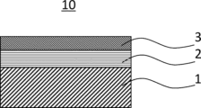
- FIG. 1 is a schematic cross-sectional view schematically showing a reflective mask blank in an embodiment of the present invention.
- FIG. 3 is a schematic cross-sectional view schematically showing a reflective mask blank in another embodiment of the present invention.
- FIG. 3 is a schematic plan view of a hole-like pattern formed in an absorption layer of a reflective mask according to an embodiment of the present invention, in which (a) shows a staggered arrangement and (b) shows an aligned arrangement.
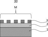
- FIG. 1 is a schematic cross-sectional view schematically showing a reflective mask in an embodiment of the present invention.
- FIG. 3 is a schematic cross-sectional view schematically showing a reflective mask in another embodiment of the present invention.
- FIG. 3 is a schematic diagram for explaining a light intensity distribution in a transfer pattern.
- the terms "on a substrate, on a layer,” and on a film include not only the case where the material is in contact with the upper surface of the film, etc., but also the upper part that is not in contact with the upper surface of the film, etc.
- film B on film A may mean that film A and film B are in contact with each other, or that another film or the like may be interposed between film A and film B.
- above here does not necessarily mean a high position in the vertical direction, but indicates a relative positional relationship.
- the thickness of the formed film, etc. can be measured using a transmission electron microscope or an X-ray reflectance method.
- the preferable numerical range can be determined by arbitrarily combining each of the preferable lower limit and upper limit.
- FIGS. 1 and 2 schematically show cross sections of the reflective mask blank of this embodiment.
- a multilayer reflective film 2 that reflects EUV light and an absorption layer 3 that absorbs EUV light are laminated on a substrate 1 in this order from the substrate 1 side.
- a protective film 4 also called a cap layer
- an antireflection film may be formed on the absorption layer 3 to facilitate pattern defect inspection after mask processing.
- the substrate 1 preferably has a low thermal expansion coefficient at 20°C, preferably 0 ⁇ 0.05 ⁇ 10 -7 /°C, more preferably 0 ⁇ It is 0.03 ⁇ 10 ⁇ 7 /°C. Further, it is preferable that the substrate 1 has excellent smoothness, high flatness, and excellent resistance (chemical resistance) to the cleaning liquid used in the manufacturing process of the reflective mask.
- the material of the substrate 1 include SiO 2 -TiO 2 glass, multi-component glass ceramics, etc., and crystallized glass in which ⁇ -quartz solid solution is precipitated, quartz glass, silicon, metal, etc. can also be used. .
- the substrate 1 is preferably smooth, and has a surface roughness (RMS) of preferably 0.15 nm or less, more preferably 0.10 nm or less. It is. From the same viewpoint, the flatness (TIR; Total Indicated Reading) is preferably 100 nm or less, more preferably 50 nm or less, and still more preferably 30 nm or less.
- RMS surface roughness
- TIR Total Indicated Reading
- the substrate 1 has high rigidity from the viewpoint of preventing deformation due to stress of a film or the like laminated thereon. Specifically, it is preferable that the Young's modulus is 65 GPa or more.
- the multilayer reflective film 2 preferably has a structure in which a plurality of layers containing elements having different refractive indexes as main components are periodically laminated.
- the multilayer reflective film 2 has a structure in which one period is a set of one high refractive index layer and one low refractive index layer, and about 40 to 60 periods are laminated.
- the high refractive index layer/low refractive index layer is generally a Mo/Si multilayer reflective film, but is not limited to this, and includes, for example, a Ru/Si multilayer reflective film, a Mo/Be multilayer reflective film, Mo compound/Si compound multilayer reflective film, Si/Mo/Ru multilayer reflective film, Si/Mo/Ru/Mo multilayer reflective film, MoRu/Si multilayer reflective film, Si/Ru/Mo multilayer reflective film, Si/Ru/Mo /Ru multilayer reflective film, etc. may also be mentioned.
- the multilayer reflective film 2 preferably has a reflectance of 60% or more, more preferably 65% or more of EUV light having a wavelength of around 13.5 nm and incident light at an incident angle of 6°.
- the thickness of each film constituting the multilayer reflective film 2 and the repetition period of lamination are appropriately set according to the film material, desired reflectance of EUV light, and the like.
- the multilayer reflective film 2 can be formed by forming each constituent film to a desired thickness using a known film forming method such as magnetron sputtering or ion beam sputtering.
- a known film forming method such as magnetron sputtering or ion beam sputtering.
- argon (Ar) gas gas pressure 1.3 ⁇ 10 ⁇ 2 to 2.7 ⁇ 10 ⁇ 2 Pa
- a Si film was first deposited to a thickness of 4.5 nm using a Si target, and then a Mo target was deposited.
- a Mo film is formed to a thickness of 2.3 nm using the following method. By repeating this as one cycle and stacking the Mo film/Si film for 30 to 60 cycles, a Mo/Si multilayer reflective film can be formed.
- the reflective mask blank of this embodiment may have a protective film 4 between the multilayer reflective film 2 and the absorption layer 3 to protect the multilayer reflective film 2 from dry etching when forming a mask pattern.
- the protective film 4 also has the role of preventing the multilayer reflective film 2 from being oxidized during EUV exposure and reducing the reflectance of EUV light.
- the etching rate ratio is preferably 10 to 200, more preferably 30 to 100. Note that as the etching gas, a halogen-based gas, an oxygen-based gas, or a mixed gas thereof is usually used.
- halogen-based gas examples include a chlorine-based gas containing one or more selected from Cl 2 , SiCl 4 , CHCl 3 , CCl 4 and BCl 3 ; selected from CF 4 , CHF 3 , SF 6 , BF 3 and XeF 2
- fluorine-based gases examples include fluorine-based gases containing one or more of the following.
- the protective film 4 contains one or more elements selected from, for example, Ru, Rh, and Si.
- the protective film 4 may be a film made only of Rh, but it is also preferable that it contains one or more elements selected from Ru, Nb, Mo, Ta, Ir, Pd, Zr, Y, and Ti.
- one or more elements selected from Ru, Ta, Ir, Pd, and Y are preferred from the viewpoint of improving resistance to etching gas and sulfuric acid peroxide used for cleaning reflective masks.
- one or more elements selected from N, O, C, and B may be included.
- the protective film 4 may be a single layer or a multilayer film consisting of multiple layers.
- the lower layer of the protective film 4 may be formed so as to contact the uppermost surface of the multilayer reflective film 2
- the upper layer of the protective film 4 may be formed so as to contact the lowermost surface of the absorbing layer 3 .
- the protective film 4 may include a layer that does not contain Rh.
- the thickness of the protective film 4 means the total thickness of the multilayer film.
- the thickness of the protective film 4 may be within a range that can sufficiently fulfill the above-mentioned role without interfering with the reflective performance of the multilayer reflective film 2, and is preferably 1.0 to 10.0 nm, more preferably 2.0 nm to 10.0 nm. It is 0 to 3.5 nm. From the same viewpoint, the protective film 4 preferably has a root mean square roughness (RMS) of 0.3 nm or less, more preferably 0.1 nm or less, and is preferably smooth.
- RMS root mean square roughness
- the protective film 4 can be formed by forming a film to a desired thickness using a known film forming method such as DC sputtering, magnetron sputtering, or ion beam sputtering.
- a buffer layer (not shown) may be formed between the protective film 4 and the absorption layer 3 to protect the multilayer reflective film 2 during dry etching or defect correction.
- the material constituting the buffer layer is not particularly limited, and examples thereof include materials containing SiO 2 , Cr, Ta, etc. as main components.
- the absorption layer 3 has a refractive index of less than 0.94 for EUV light with a wavelength of 13.5 nm, and an extinction coefficient of 0.060 or less, and is a multilayer reflective film 2 for the incident light of EUV light with a wavelength of 13.5 nm.
- the phase difference between the light reflected from the surface of the absorption layer 3 and the light reflected from the surface of the absorption layer 3 is 220 to 320°.
- the reflective mask blank of this embodiment is suitable for a reflective mask for EUV lithography that can transfer a fine hole-like pattern with high dimensional accuracy because the absorption layer 3 has such characteristics.
- the refractive index of the absorption layer 3 for EUV light with a wavelength of 13.5 nm is less than 0.94, preferably 0.93 or less, and more preferably 0.92 or less.
- the refractive index is preferably 0.85 or more.
- the extinction coefficient of EUV light with a wavelength of 13.5 nm of the absorption layer 3 is 0.060 or less, preferably 0.010 to 0.050, more preferably 0.020 to 0.045, and even more preferably 0.060. 030 to 0.040.
- phase difference is 220 to 320°, preferably 220 to 280°, more preferably 220 to 260°. Note that the method for measuring the phase difference will be described later. Moreover, the above-mentioned phase difference is a value calculated by an optical multilayer simulation described later. By having a phase difference within the above range, a phase shift mask capable of transferring a fine hole-like pattern with high dimensional accuracy can be obtained.
- the reflected light from the surface of the multilayer reflective film 2 in the phase shift mask passes through the opening of the mask pattern without passing through the absorption layer 3, and passes through the (protective film 4 and) the multilayer reflective film.
- EUV light with a wavelength of 13.5 nm that was directly incident on the multilayer reflective film 2 is reflected by the multilayer reflective film 2 and passed through the opening of the mask pattern without passing through the absorption layer 3 again.
- reflected light from the surface of the absorption layer 3 means that incident light of EUV light with a wavelength of 13.5 nm is transmitted through the absorption layer 3 (and protective film 4) while being absorbed by the absorption layer 3, and the multilayer reflection film 2 This means the reflected light that is reflected by the absorption layer 3 and transmitted through the absorption layer 3 while being absorbed by the absorption layer 3 again.
- the absorption layer of a reflective mask for EUV lithography is desirably thin from the viewpoint of suppressing shadowing, and various constituent materials and structures have been studied. was considered the best.
- the phase difference uses a value calculated by optical multilayer simulation, but can be roughly expressed by the following formula (1).
- ⁇ is the phase difference
- d is the thickness of the absorption layer 3
- ⁇ is the wavelength of the incident light
- n is the refractive index of the absorption layer 3.
- Examples of the mask pattern formed on the absorption layer 3 of the reflective mask blank 10 include a mask pattern including periodically arranged hole-shaped patterns.
- the mask pattern formed on the absorption layer 3 of the reflective mask blank 10 may have a staggered arrangement as shown in FIG. 3(a), or may have an aligned arrangement as shown in FIG. 3(b).
- the width (H1) of the holes H and the interval (H2) between the holes H are both equal, but the width (H1) and the interval (H2) are , the width (H1) and the interval (H2) may be different. Note that in this specification, "width of a hole” means the major axis of the hole.
- EUV lithography is a reduction projection exposure.
- the numerical aperture (NA) of the lens of the exposure device is 0.33
- the reduction ratio of the transferred pattern to the mask pattern is 4 times in the vertical direction (X direction) and 4 times in the horizontal direction (Y direction).
- the dimensions of the hole H are four times the width of the hole in the transfer pattern both vertically (in the X direction) and horizontally (in the Y direction).
- the numerical aperture (NA) of the lens of the exposure device is 0.55
- the reduction ratio of the transferred pattern with respect to the mask pattern is 4 times in the vertical direction (X direction) and 8 times in the horizontal direction (Y direction).
- the length (X direction) of the hole H is four times the hole width of the transfer pattern
- the width (Y direction) is eight times the hole width of the transfer pattern.
- the transfer pattern formed by the hole-like pattern includes a fine hole-like pattern with a hole width of 22 nm or less when the numerical aperture (NA) of the lens of the exposure device is 0.33, for example.
- NA numerical aperture
- the NA 0.55
- the hole width of the transfer pattern is within the above range, more excellent effects as a phase shift mask with high dimensional accuracy can be obtained.
- the material constituting the absorption layer 3 is not particularly limited as long as it can form the phase shift mask as described above, and includes, for example, ruthenium (Ru), rhenium (Re), iridium (Ir), Examples include materials containing osmium (Os) and platinum (Pt).
- the material constituting the absorption layer 3 preferably contains ruthenium (Ru), and further contains tantalum (Ta), tungsten (W), chromium (Cr), molybdenum (Mo), niobium (Nb), and osmium ( It is more preferable that the metal element contains one or more metal elements selected from Os), iridium (Ir), rhenium (Re), and rhodium (Rh).
- the metal elements may be used alone or in combination of two or more.
- the composition ratio of each metal is not particularly limited as long as the refractive index and extinction coefficient of the absorption layer 3 satisfy the above numerical ranges.
- the above-mentioned material may be a single metal element or an alloy, or may be a compound containing, for example, oxygen (O), nitrogen (N), carbon (C), boron (B), hydrogen (H), etc. .
- the ratio of the Ru content [at%] to the Ta content [at%] is preferably 10 to 97, more preferably 15 to 96, more preferably 18 to 95.5, even more preferably 20 to 50. If Ru/Ta is 10 or more, the hydrogen resistance of the phase shift film 13 is likely to be improved, and if it is 97 or less, the etching selectivity is large and the processability of the phase shift film 13 is likely to be good.
- the ratio of the Ru content [at%] to the Cr content [at%] is preferably 1 to 13, more preferably 1 to 6, more preferably 1.5 to 5.7, even more preferably 1.8 to 5.6.
- Ru/Cr is 1 or more, the hydrogen resistance of the phase shift film 13 is easily improved, and when it is 13 or less, the etching selectivity is large and the processability of the phase shift film 13 is likely to be good.
- the ratio of the Ru content [at%] to the W content [at%] is preferably 1 to 20, more preferably 2 to 18, more preferably 2-15, even more preferably 2-9. If Ru/Cr is 1 or more, the hydrogen resistance of the phase shift film 13 is likely to be improved, and if it is 20 or less, the etching selectivity is large and the processability of the phase shift film 13 is likely to be good.
- the total content [at%] of these elements is preferably 1 to 75 at%, more preferably 2 at%. ⁇ 72 at%, more preferably 3 to 50 at%, even more preferably 5 to 30 at%, particularly preferably 7 to 20 at%.
- the absorbent layer 3 may have a multilayer structure in which two or more layers are laminated.
- a multilayer structure is preferable in that the entire absorbent layer 3 can be designed with each layer having a predetermined functional layer made of different materials.
- Functional layers include, for example, a buffer layer that is formed between the reflective layer and the absorbing layer as necessary to prevent damage to the reflective layer during patterning, and a buffer layer that improves the contrast during mask pattern inspection.
- a low reflection layer (a low reflection layer in the wavelength range of the mask pattern inspection light) formed as necessary on the top layer of the absorption layer 3 for the purpose of controlling the reflectance at EUV wavelengths. Examples include a phase control layer formed for the purpose of controlling the phase at EUV wavelength.
- layer combinations in the multilayer structure include Ru/Ta 2 O 5 , Ru/Cr 2 O 3 , Ir/Ta 2 O 5 , Ir/Ru, Pt/Ru, and the like.
- the constituent materials of these layers such as Ru, Ta 2 O 5 , Cr 2 O 3 , Ir, Pt, etc. may be alloys, nitrogen substances, acid It may also be a nitride, a boride, or the like.
- the lamination order may be any order; for example, in the case of the above-mentioned two-layer structure, the order is preferably first layer/second layer.
- the refractive index and extinction coefficient are obtained as a weighted average value taking into account the thickness of each layer.
- the absorption layer 3 can be formed by forming each constituent film to a desired thickness using a known film forming method such as magnetron sputtering or ion beam sputtering.
- the total thickness of the absorption layer 3 is 60 nm or less, and it can exhibit the effect as a phase shift mask that can transfer a fine hole-like pattern with high dimensional accuracy while suppressing shadowing.
- the total thickness of the absorption layer 3 is preferably thin from the viewpoint of etching efficiency during film formation of the absorption layer 3 and mask pattern formation, and is preferably 60 nm or less, more preferably 58 nm or less, and even more preferably 53 nm or less. It is. Further, the total thickness of the absorption layer 3 is preferably 20 nm or more from the viewpoint of the absorption effect of EUV light.
- An antireflection film (not shown) may be laminated on the absorption layer 3 to prevent reflection when DUV light (deep ultraviolet light) with a wavelength of 190 to 260 nm is used in the inspection process.
- the reflective mask is sometimes inspected for defects in the mask pattern formed on the absorption layer 3.
- the presence or absence of defects is determined mainly based on the optical data of the reflected light of the inspection light. Therefore, the light that passes through the mask cannot be used as the inspection light, and DUV light is used. For this reason, when the above-mentioned mask inspection is performed, it is preferable to provide an antireflection film on the absorption layer 3 to prevent reflection of DUV light, which is the inspection light, for accurate inspection.
- the antireflection film is preferably formed of a material that has a lower refractive index for DUV light than the absorption layer 3.
- the constituent material of the antireflection film include a material containing Ta as a main component and one or more components selected from Hf, Ge, Si, B, N, H, and O in addition to Ta. Specific examples include TaO, TaON, TaONH, TaHfO, TaHfON, TaBSiO, TaBSiON, and the like.
- the antireflection film can be formed by forming a film to a desired thickness using, for example, a known film forming method such as magnetron sputtering or ion beam sputtering.
- the reflective mask blank of this embodiment may be provided with a known functional film for reflective mask blanks.
- a back conductive film may be formed on the surface (back surface) opposite to the multilayer reflective film 2 of the substrate 1. good.
- the back conductive film preferably has a sheet resistance of 100 ⁇ / ⁇ or less, and a known configuration can be applied.
- the constituent material of the back conductive film include Si, TiN, Mo, Cr, TaSi, and the like.
- the thickness of the back conductive film can be, for example, 10 to 1000 nm.
- the back conductive film is formed to a desired thickness using a known film forming method such as magnetron sputtering, ion beam sputtering, chemical vapor deposition (CVD), vacuum evaporation, or electroplating. It can be formed by coating.
- a known film forming method such as magnetron sputtering, ion beam sputtering, chemical vapor deposition (CVD), vacuum evaporation, or electroplating. It can be formed by coating.
- the reflective mask blank of the present invention has a reflectance of EUV light of preferably 2.0 to 30%, more preferably 3.0 to 25%, still more preferably 5.0 to 20%, even more preferably 6. .0 to 15.0%, particularly preferably 8.0 to 10%.
- the reflective mask 30 shown in FIG. 4 is a reflective mask for EUV lithography in which a multilayer reflective film 2 that reflects EUV light and an absorption layer 3 that absorbs EUV light are laminated in this order from the substrate 1 side on a substrate 1. type mask, the absorption layer 3 has a refractive index of less than 0.94 for EUV light with a wavelength of 13.5 nm, an extinction coefficient of 0.060 or less, and absorbs incident light of EUV light with a wavelength of 13.5 nm.
- the phase difference between the light reflected from the surface of the multilayer reflective film 2 and the light reflected from the surface of the absorption layer 3 is 220 to 320°, preferably 220 to 280°, and the absorption layer 3 has a mask pattern M. It is being formed. As shown in FIG. 5, a protective film 4 may be formed between the multilayer reflective film 2 and the absorption layer 3 to protect the multilayer reflective film 2 from dry etching when forming a mask pattern.
- the reflective mask of the present invention has a mask pattern M formed on the absorption layer 3 of the reflective mask blank 10 of the present embodiment. Therefore, the description of each constituent layer of the reflective mask 30 is the same as that of the reflective mask blank 10 described above, and will therefore be omitted.
- the mask pattern M preferably includes a periodically arranged hole pattern from the viewpoint of supporting a more complex semiconductor circuit.
- the reflective mask 30 has a normalized image log slope (NILS) of the hole-like pattern, preferably 1.4 or more, more preferably 1.5 or more, More preferably, it is 2.0 or more.
- NILS normalized image log slope
- the reflective mask 30 has holes in the transfer pattern formed by the hole-like pattern, for example, if the numerical aperture (NA) of the lens of the exposure device is 0.33, It is suitable when the material includes a fine hole-like pattern with a width of 22 nm or less, and when NA is 0.55, it is suitable when the material contains a fine hole-like pattern with a hole width of 14 nm or less. When the hole width is within the above range, a more excellent effect as a phase shift mask with high dimensional accuracy can be obtained.
- NA numerical aperture
- the present invention provides high dimensional accuracy when the phase difference between the light reflected from the multilayer reflective film and the light reflected from the absorption layer is larger than before in the absorbing layer in a mask including a fine hole-like pattern in EUV lithography. This is based on the discovery that it is possible to form a transfer pattern using Further, the present inventor focused on the refractive index n, extinction coefficient k, and phase difference of the absorption layer 3 for EUV light, and found that there is a range in which high transfer accuracy can be achieved in an EUV mask including a hole-like pattern. I found out.
- the excellent transfer accuracy by the reflective mask 30 can be estimated from the normalized image log slope (NILS).
- NILS is a characteristic value indicating the contrast between bright and dark areas of light intensity in a transferred pattern. It can be said that the higher the value of NILS, the higher the contrast of the transferred pattern and the better the transfer accuracy.
- NILS is determined by the following formula (2).
- I(x) is the light intensity distribution in the transfer pattern (intensity normalized by the maximum intensity, dimensionless quantity), and x is the distance from the peak position in the hole width direction of the transfer pattern (unit: nm) ), CD represents the critical dimension of the hole width at the resolution limit of the transfer pattern. Note that in this specification, CD corresponds to the hole width of the transfer pattern.
- FIG. 6 shows an outline of the light intensity distribution I(x).
- NILS is the slope of lnI(x) (natural logarithm of I(x)) when the width (x 2 - x 1 ) at the peak of I(x) is equal to CD, as shown in FIG. It is obtained as the product of CD.
- I(x) is based on known optical imaging theory (for example, Koichi Matsumoto, "Lithography Optics”, “Optics”, Optical Society of Japan, March 2001, Vol. 30, No. 3, p. 40-47) (Reference) is determined by lithography simulation.
- optical imaging theory for example, Koichi Matsumoto, "Lithography Optics”, “Optics”, Optical Society of Japan, March 2001, Vol. 30, No. 3, p. 40-47
- Reference is determined by lithography simulation.
- commercially available software for example, lithography simulator "PROLITH”, manufactured by KLA-Tencor; "Sentaurus Lithography”, manufactured by Synopsis, etc.
- simulations were performed assuming that the numerical aperture NA of the lens of the EUV exposure apparatus was 0.33, or 0.55 in consideration of a next-generation model aimed at further miniaturization of patterns.
- the refractive index n is 0.88 to 0.96
- the extinction coefficient k is 0.015 to 0.065
- the absorption layer thickness d Calculations were performed repeatedly while changing the value in the range of 20 to 80 nm, and d (optimal value) at which the NILS was maximized was determined at predetermined n and k. Furthermore, the optimum value of the phase difference was determined from the values of d, n, and k at this time.
- each alloy is Ru 0.7 Cr 0.3 , Ru 0.7 Ta 0.3 , Ru 0.5 W 0 It was set as .5 . Strictly speaking, the optical constants of each alloy may vary slightly depending on the density and film forming conditions, so representative values were used. Further, the first layer and the second layer in Table 2 mean that they are formed in this order from the substrate 1 side.
- the NILS is high and the contrast of the transferred pattern is high.
- the phase difference between the light reflected from the surface of the multilayer reflective film 2 and the light reflected from the surface of the absorption layer 3 is 220 to 320 degrees, and even if the total thickness is 60 nm or less, the dimensional accuracy is It can be said that a transfer pattern with high quality can be obtained.
- n is, the more preferable it is, for example, a suitable range is n less than 0.94, more preferably 0.93 or less, still more preferably 0.92 or less.
- the extinction coefficient k has a smaller influence than the refractive index n, it can be seen that the NILS increases in a region where k is low.
- a suitable range is for k to be 0.06 or less, more preferably 0.05 or less, still more preferably 0.04 or less. It can be seen that the phase difference at this time varies depending on the refractive index n and extinction coefficient k of the material, but falls within the range of 220 to 230°. Similarly, in FIGS.
- the extinction coefficient k has a smaller effect than the refractive index n, but from the viewpoint of compatibility with various CDs, the preferred range is similarly that k is 0.06 or less, and It is preferably 0.05 or less, more preferably 0.04 or less.
- the phase difference at this time varies depending on the refractive index n and extinction coefficient k of the material, but is 230 to 270°, and it can be seen that the narrower the CD, the higher the optimal phase difference.
- phase difference that takes the maximum value of NILS increases when the CD becomes narrower is considered as follows.
- a phase shift mask provides a reversal phase difference to light transmitted through the transparent portions of the mask pattern by making the transparent portions of a different material or shape from the adjacent transparent portions.
- the electric field of light changes continuously at the interface between a transparent part on the mask pattern and an adjacent transparent part.
- the period of the unevenness of the EUV mask pattern becomes smaller. Therefore, the electric field of light inside the pattern structure of the EUV mask is bent significantly in a shorter period than when the CD is large.
- the CD of the EUV mask structure when it is made narrower than when it is sufficiently large compared to the wavelength, the contribution of electric field distortion inside the concavo-convex pattern increases, and as a result, the transmission part of the mask pattern and It is thought that a phenomenon occurs in which the average phase difference between adjacent transparent parts becomes smaller than the intended value (that is, the value calculated by the above simulation or the above equation (1)). Therefore, if the CD is narrow, the thickness of the mask is adjusted in advance to create a mask that can provide a larger phase difference than the conventional one as calculated by the above simulation or the above formula (1). By doing so, it becomes possible to realize the effect of a phase shift mask.
- FIG. 3 is a diagram showing a distribution of phase difference values. It can be seen from FIG. 8 that as the CD becomes narrower, the thickness of the absorption layer that takes the maximum value of NILS becomes thicker, and the optimum value of the phase difference corresponding to this becomes higher.
- Table 4 is organized by film thickness when NILS in the 4x direction is maximum.
- the reason why the NILS in the 4x direction was selected as a reference is because the concavo-convex period of the EUV mask pattern is smaller than that in the 8x direction, so that the contribution of the distortion of the electric field inside the above-mentioned concavo-convex pattern becomes larger.
- the irregularity period of the EUV mask pattern is smaller in the 4x direction than in the 8x direction, making it difficult to process. It is desirable to do so.
- the NILS may be high and the contrast of the transferred pattern may be high.
- the phase difference between the light reflected from the surface of the multilayer reflective film 2 and the light reflected from the surface of the absorption layer 3 is 220 to 320 degrees, and even if the total thickness is 60 nm or less, the dimensional accuracy is It can be said that a transfer pattern with high quality can be obtained.
- the reflective mask 30 can be manufactured by forming a mask pattern M using the reflective mask blank 10 by applying a known lithography technique. For example, a photoresist film is formed on the absorption layer 3 of the reflective mask blank 10, processed into a resist pattern having a desired pattern shape, and after etching the absorption layer 3 by dry etching or the like, the resist pattern is By removing unnecessary photoresist including , a reflective mask 30 in which a mask pattern M is formed on the absorption layer 3 can be obtained.
- the part of the absorption layer 3 from which the photoresist has been removed is the transmission part, and the part of the absorption layer 3 from which the photoresist has not been removed is the area between the two transmission parts.
- a mask pattern M is configured.
- Substrate 2 Multilayer reflective film 3
- Absorption layer 4 Protective film 10, 20 Reflective mask blank 30, 40
- Reflective mask H Hole-shaped hole H1 Width of hole H2 Spacing between holes X Vertical (X direction) Y horizontal (Y direction) M mask pattern
Landscapes
- Physics & Mathematics (AREA)
- General Physics & Mathematics (AREA)
- Preparing Plates And Mask In Photomechanical Process (AREA)
- Exposure Of Semiconductors, Excluding Electron Or Ion Beam Exposure (AREA)
Abstract
Provided are a reflective mask for EUV lithography that can form transfer patterns with high dimensional accuracy in fine hole-like patterns, and a reflective mask blank used for said reflective mask. A reflective mask blank 10 for EUV lithography in which a multilayer reflective film 2 that reflects EUV light and an absorption layer 3 that absorbs EUV light are layered on a substrate 1 in the stated order from the substrate 1 side, wherein: the absorption layer 3 has a refractive index of less than 0.94 and an extinction coefficient of 0.060 or less for EUV light having a wavelength of 13.5 nm; and the phase difference between light reflected from the surface of the multilayer reflective film and the light reflected from the surface of the absorption layer, with respect to incident light of EUV light having a wavelength of 13.5 nm, is 220-320°. Additionally, a reflective mask obtained by forming a mask pattern on the absorption layer 3.
Description
本発明は、半導体製造等における極端紫外線(EUV;Extreme Ultraviolet)リソグラフィに用いられる反射型マスクブランク、及びこれを用いた反射型マスクに関する。
The present invention relates to a reflective mask blank used in extreme ultraviolet (EUV) lithography in semiconductor manufacturing and the like, and a reflective mask using the same.
EUVリソグラフィに用いられる反射型マスクは、波長13.5nm程度の短波長のEUV光を反射する多層反射膜の上に、EUV光を吸収する吸収層によるマスクパターンが設けられている。反射型マスクは、吸収層が厚いと、斜め(通常、入射角6°)に入射するEUV光及びその反射光が遮られる、いわゆるシャドーイングによって、転写パターンの寸法誤差が生じやすくなる。
A reflective mask used in EUV lithography has a mask pattern made of an absorption layer that absorbs EUV light on a multilayer reflective film that reflects EUV light with a short wavelength of about 13.5 nm. When a reflective mask has a thick absorption layer, dimensional errors in the transferred pattern are likely to occur due to so-called shadowing, in which obliquely incident (usually at an incident angle of 6 degrees) EUV light and its reflected light are blocked.
このようなシャドーイングによる寸法誤差の抑制のため、マスクの吸収層の膜厚はできるだけ小さくすることが検討されている。また、EUV光を吸収するとともに、多層反射膜からの反射光とは位相が異なる反射光となるように形成された吸収層により、転写パターンのエッジ部のコントラストを向上させる、位相シフトマスクの技術開発も進められている。
In order to suppress dimensional errors caused by such shadowing, it is being considered to reduce the thickness of the absorption layer of the mask as much as possible. In addition, phase shift mask technology improves the contrast of the edge portion of the transferred pattern by absorbing EUV light and using an absorption layer formed so that the reflected light has a different phase from the reflected light from the multilayer reflective film. Development is also underway.
ところで、透過型の位相シフトマスクは、マスクパターンの透過部に、当該透過部とは屈折率や透過率が異なる物質又は形状を付与して、この部分の光の位相を変化させて、解像度を向上させるものである。位相を変化させた領域では、位相差を有する透過回折光同士が干渉し合い、光強度が低下する。これにより、転写パターンのコントラストが向上し、結果的に転写時の焦点深度が拡大するとともに転写精度が向上する。
透過型の位相シフトマスクの一種であるハーフトーン型マスクは、透過光の位相を変化させる部分に、露光光に対する半透過性の薄膜が形成されている。ハーフトーン型マスクは、透過率を数%程度(通常、基板透過光に対して2.5~15.0%程度)まで減衰させつつ、位相を変化させて、パターンエッジ部の解像度を向上させることにより、転写精度を向上させることができる。
なお、位相差は、原理上、180°が最良であるが、実質的に175~185°程度であれば、解像度の向上効果が得られることが知られている。 By the way, in a transmission-type phase shift mask, a material or shape that has a different refractive index or transmittance than the transmission part is added to the transmission part of the mask pattern, and the phase of light in this part is changed to improve the resolution. It is something that improves. In the region where the phase is changed, the transmitted diffracted lights having a phase difference interfere with each other, and the light intensity decreases. As a result, the contrast of the transferred pattern is improved, and as a result, the depth of focus during transfer is expanded and the transfer accuracy is improved.
A halftone mask, which is a type of transmission phase shift mask, has a thin film semi-transparent to exposure light formed in a portion that changes the phase of transmitted light. Halftone masks improve the resolution of pattern edges by attenuating the transmittance to about a few percent (usually about 2.5 to 15.0% of the light transmitted through the substrate) and changing the phase. By doing so, the transfer accuracy can be improved.
Note that, in principle, the best phase difference is 180°, but it is known that an effect of improving resolution can be obtained if the phase difference is substantially about 175 to 185°.
EUVリソグラフィ用反射型マスクにおいても、位相シフト効果による解像度向上の原理は同じであり、透過型マスクにおける「透過率」を「反射率」に置き換えればよいと考えられていた。すなわち、吸収層におけるEUV光の反射率が2.5~15.0%であり、かつ、反射層からのEUV光の反射光と、吸収層からのEUV光の反射光との位相差(以下、単に「位相差」とも言う。)が175~185°であることが望ましいと考えられていた。
このため、従来の反射型マスクにおける位相シフトマスクは、位相差が180°前後(ほぼ反転)となるように設計されることが一般的であった(例えば、特許文献1参照)。 In reflective masks for EUV lithography, the principle of resolution improvement due to the phase shift effect is the same, and it was thought that "transmittance" in transmission masks could be replaced with "reflectance." That is, the reflectance of EUV light in the absorption layer is 2.5 to 15.0%, and the phase difference (hereinafter referred to as , also simply referred to as "phase difference") was considered desirable to be 175 to 185 degrees.
For this reason, a phase shift mask in a conventional reflective mask is generally designed so that the phase difference is around 180° (almost inverted) (for example, see Patent Document 1).
一方で、反射型マスクにおいては、光が垂直に透過する透過型マスクとは異なり、光が斜めに入射することから、近年、最適な位相差は216°(=1.2π)であるとの報告もある。
On the other hand, in a reflective mask, unlike a transmissive mask in which light is transmitted perpendicularly, light enters the mask obliquely, and in recent years it has been found that the optimal phase difference is 216° (=1.2π). There are also reports.
このため、反射型マスクの吸収層は、構成材料の屈折率(以下、nと表す場合もある。)及び消衰係数(以下、kと表す場合もある。)に基づいて、位相差が180°又は216°になるように、膜厚を設定するという設計がなされてきたが、吸収層の反射率や位相差、膜厚の最適値は、露光条件や転写パターン形状等によって異なり、一概に決めることは難しい。
Therefore, the absorption layer of a reflective mask has a phase difference of 180 mm based on the refractive index (hereinafter sometimes referred to as n) and extinction coefficient (hereinafter sometimes referred to as k) of the constituent materials. Although designs have been made to set the film thickness so that the angle of It's difficult to decide.
近年、コンピューターや電気機器の主要部分には、多数のMOSトランジスタ、抵抗、キャパシタ等を一つのチップ上に集積化する大規模集積回路(LSI)が採用されている。LSIの中でも、例えば、DRAM(Dynamic Random Access Memory)などの素子においては、急速な微細化が進み、これに伴ってMOSトランジスタや抵抗などの配線ラインあるいはコンタクトホールなどが露光技術の限界に近いレベルまで微細化されてきている。これに伴い、パターンの微細化の要求はさらに高まっており、パターン形成工程もより複雑になっている。
ホール状パターンの微細化加工において、素子に転写されたホール状パターンのホール幅が狭くなる程、加工が難しくなる。EUV露光装置の仕様により露光装置のレンズの開口数(NA)は異なり、NAによって、加工可能な転写パターンのホール幅も異なる。例えば、NAが0.33では転写パターンのホール幅が22nm以下、NAが0.55では転写パターンのホール幅が14nm以下になると、上記のような位相シフトマスクであっても、転写パターンを高精度で形成することは困難になることが想定される。 In recent years, large-scale integrated circuits (LSIs), which integrate a large number of MOS transistors, resistors, capacitors, etc. on a single chip, have been used in major parts of computers and electrical equipment. Among LSI devices, for example, elements such as DRAM (Dynamic Random Access Memory) are becoming rapidly miniaturized, and as a result, wiring lines and contact holes for MOS transistors and resistors are reaching a level that is close to the limit of exposure technology. It has become even more miniaturized. Along with this, the demand for finer patterns has further increased, and the pattern forming process has also become more complex.
In microfabrication processing of a hole-like pattern, the narrower the hole width of the hole-like pattern transferred to the element, the more difficult the processing becomes. The numerical aperture (NA) of the lens of the exposure device varies depending on the specifications of the EUV exposure device, and the hole width of the transfer pattern that can be processed also varies depending on the NA. For example, when the NA is 0.33, the hole width of the transferred pattern is 22 nm or less, and when the NA is 0.55, the hole width of the transferred pattern is 14 nm or less, even with the above phase shift mask. It is assumed that it will be difficult to form with precision.
特に、半導体集積回路向けのマスクはLSI集積密度の上昇に伴って複雑化が進み、転写に使われるマスクに描画されるパターンもより複雑な形状に対応する必要がある。
EUVリソグラフィ用反射型マスクにおいては、転写パターンのホール幅が小さいほどシャドーイングの影響を受けやすい。このため、転写精度に優れたマスクパターンを形成するためには、予め、最適な反射率や位相差が得られる吸収層を備えた位相シフトマスクの開発が求められている。 In particular, masks for semiconductor integrated circuits are becoming more and more complex as LSI integration density increases, and the patterns drawn on the masks used for transfer must also accommodate more complex shapes.
In a reflective mask for EUV lithography, the smaller the hole width of the transfer pattern, the more susceptible it is to shadowing. Therefore, in order to form a mask pattern with excellent transfer accuracy, there is a need to develop a phase shift mask that includes an absorbing layer that provides optimal reflectance and phase difference.
本発明は、このような状況に鑑みてなされたものであり、微細なホール状パターンにおいて、寸法精度の高い転写パターンを形成できるEUVリソグラフィ用反射型マスク、及びこれに用いられる反射型マスクブランクを提供することを目的とする。
The present invention was made in view of these circumstances, and provides a reflective mask for EUV lithography that can form a transfer pattern with high dimensional accuracy in a fine hole pattern, and a reflective mask blank used therein. The purpose is to provide.
本発明は、EUVリソグラフィにおいて、微細なホール状パターンにおいて、吸収層で、多層反射膜からの反射光と吸収層からの反射光との位相差が従来よりも大きい場合に、高い寸法精度での転写パターンの形成が可能となることを見出したことに基づく。
In EUV lithography, the present invention can be applied to fine hole-like patterns in an absorbing layer with high dimensional accuracy when the phase difference between the reflected light from the multilayer reflective film and the reflected light from the absorbing layer is larger than before. This is based on the discovery that it is possible to form a transfer pattern.
すなわち、本発明は下記のとおりである。
[1]基板上に、EUV光を反射する多層反射膜と、EUV光を吸収する吸収層とが、この順に前記基板側から積層されたEUVリソグラフィ用反射型マスクブランクであって、前記吸収層は、波長13.5nmのEUV光の屈折率が0.94未満、かつ、消衰係数が0.060以下であり、波長13.5nmのEUV光の入射光に対する、前記多層反射膜の表面からの反射光と、前記吸収層の表面からの反射光との位相差が、220~320°である、反射型マスクブランク。
[2]前記位相差が、220~280°である、[1]に記載の反射型マスクブランク。
[3]前記消衰係数が、0.050以下である、[1]又は[2]に記載の反射型マスクブランク。
[4]前記消衰係数が、0.040超0.050以下である、[1]~[3]のいずれかにに記載の反射型マスクブランク。
[5]前記吸収層に、周期的に配置されたホール状パターンを含むマスクパターンを形成する、[1]~[4]のいずれかに記載の反射型マスクブランク。
[6]前記ホール状パターンにより形成される転写パターンのホール幅は、露光装置のレンズの開口数が0.33において22nm以下であり、露光装置のレンズの開口数が0.55において14nm以下である、[5]に記載の反射型マスクブランク。
[7]前記吸収層は、ルテニウム(Ru)を含む、[1]~[6]のいずれかに記載の反射型マスクブランク。
[8]前記吸収層は、タンタル(Ta)、タングステン(W)、クロム(Cr)、モリブデン(Mo)、ニオブ(Nb)、オスミウム(Os)、イリジウム(Ir)、レニウム(Re)、及びロジウム(Rh)から選ばれる1種以上の金属元素を含む、[7]に記載の反射型マスクブランク。
[9]前記吸収層は、2層以上の膜が積層されてなる、[1]~[8]のいずれかに記載の反射型マスクブランク。
[10]前記吸収層は、総厚さが60nm以下である、[1]~[9]のいずれかに記載の反射型マスクブランク。
[11]前記多層反射膜と前記吸収層との間に、前記多層反射膜を保護する保護膜を有する、[1]~[10]のいずれかに記載の反射型マスクブランク。 That is, the present invention is as follows.
[1] A reflective mask blank for EUV lithography in which a multilayer reflective film that reflects EUV light and an absorption layer that absorbs EUV light are laminated in this order from the substrate side on a substrate, and the absorption layer has a refractive index of less than 0.94 for EUV light with a wavelength of 13.5 nm, and an extinction coefficient of 0.060 or less, and is A reflective mask blank, wherein the phase difference between the reflected light from the surface of the absorption layer and the reflected light from the surface of the absorption layer is 220 to 320°.
[2] The reflective mask blank according to [1], wherein the phase difference is 220 to 280°.
[3] The reflective mask blank according to [1] or [2], wherein the extinction coefficient is 0.050 or less.
[4] The reflective mask blank according to any one of [1] to [3], wherein the extinction coefficient is greater than 0.040 and less than or equal to 0.050.
[5] The reflective mask blank according to any one of [1] to [4], wherein a mask pattern including a periodically arranged hole-like pattern is formed in the absorption layer.
[6] The hole width of the transfer pattern formed by the hole-shaped pattern is 22 nm or less when the numerical aperture of the lens of the exposure device is 0.33, and is 14 nm or less when the numerical aperture of the lens of the exposure device is 0.55. A reflective mask blank according to [5].
[7] The reflective mask blank according to any one of [1] to [6], wherein the absorption layer contains ruthenium (Ru).
[8] The absorption layer contains tantalum (Ta), tungsten (W), chromium (Cr), molybdenum (Mo), niobium (Nb), osmium (Os), iridium (Ir), rhenium (Re), and rhodium. The reflective mask blank according to [7], containing one or more metal elements selected from (Rh).
[9] The reflective mask blank according to any one of [1] to [8], wherein the absorption layer is formed by laminating two or more layers.
[10] The reflective mask blank according to any one of [1] to [9], wherein the absorption layer has a total thickness of 60 nm or less.
[11] The reflective mask blank according to any one of [1] to [10], further comprising a protective film for protecting the multilayer reflective film between the multilayer reflective film and the absorption layer.
[12]基板上に、EUV光を反射する多層反射膜と、EUV光を吸収する吸収層とが、この順に前記基板側から積層されたEUVリソグラフィ用反射型マスクであって、前記吸収層は、波長13.5nmのEUV光の屈折率が0.94未満、かつ、消衰係数が0.060以下であり、波長13.5nmのEUV光の入射光に対する、前記多層反射膜の表面からの反射光と、前記吸収層の表面からの反射光との位相差が、220~320°であり、前記吸収層にマスクパターンが形成されている、反射型マスク。
[13]前記位相差が、220~280°である、[12]に記載の反射型マスク。
[14]前記消衰係数が、0.050以下である、[12]又は[13]に記載の反射型マスク。
[15]前記消衰係数が、0.040超0.050以下である、[13]又は[14]に記載の反射型マスク。
[16]前記マスクパターンが、周期的に配置されたホール状パターンを含む、[12]~[15]のいずれかに記載の反射型マスク。
[17]前記ホール状パターンのホールの幅は、露光装置のレンズの開口数が0.33の場合、22nm以下であり、露光装置のレンズの開口数が0.55の場合、14nm以下である、[16]に記載の反射型マスク。
[18]前記多層反射膜と前記吸収層との間に、前記多層反射膜を保護する保護膜を有する、[12]~[17]のいずれかに記載の反射型マスク。 [12] A reflective mask for EUV lithography in which a multilayer reflective film that reflects EUV light and an absorption layer that absorbs EUV light are laminated in this order from the substrate side on a substrate, the absorption layer being , the refractive index of EUV light with a wavelength of 13.5 nm is less than 0.94, and the extinction coefficient is 0.060 or less, and the refractive index from the surface of the multilayer reflective film with respect to the incident light of EUV light with a wavelength of 13.5 nm is A reflective mask, wherein a phase difference between reflected light and reflected light from a surface of the absorption layer is 220 to 320°, and a mask pattern is formed on the absorption layer.
[13] The reflective mask according to [12], wherein the phase difference is 220 to 280°.
[14] The reflective mask according to [12] or [13], wherein the extinction coefficient is 0.050 or less.
[15] The reflective mask according to [13] or [14], wherein the extinction coefficient is greater than 0.040 and less than or equal to 0.050.
[16] The reflective mask according to any one of [12] to [15], wherein the mask pattern includes a periodically arranged hole pattern.
[17] The width of the hole in the hole-like pattern is 22 nm or less when the numerical aperture of the lens of the exposure device is 0.33, and is 14 nm or less when the numerical aperture of the lens of the exposure device is 0.55. , the reflective mask described in [16].
[18] The reflective mask according to any one of [12] to [17], further comprising a protective film for protecting the multilayer reflective film between the multilayer reflective film and the absorption layer.
本発明によれば、微細なホール状パターンにおいて、寸法精度の高い転写パターンを形成できるEUVリソグラフィ用反射型マスク、及びこれに用いられる反射型マスクブランクが提供される。
According to the present invention, there are provided a reflective mask for EUV lithography that can form a transfer pattern with high dimensional accuracy in a fine hole-like pattern, and a reflective mask blank used therein.
まず、本明細書における表記の説明を述べる。
基板上、層上及び膜上(以下、膜等上と略称する。)とは、膜等の上面に接する場合のみならず、膜等の上面に接していない上方も含む意味である。例えば、「膜A上の膜B」とは、膜Aと膜Bとが接していてもよく、膜Aと膜Bとの間に他の膜等が介在していてもよい。また、ここで言う「上」とは、必ずしも鉛直方向における高い位置を意味する場合に限られず、相対的な位置関係を示すものである。
成膜した膜等の厚さは、透過型電子顕微鏡やX線反射率法により測定できる。
好ましい数値範囲は、好ましい下限値及び上限値のそれぞれを任意に組み合わせることができる。 First, the notation used in this specification will be explained.
The terms "on a substrate, on a layer," and on a film (hereinafter abbreviated as "on a film, etc.") include not only the case where the material is in contact with the upper surface of the film, etc., but also the upper part that is not in contact with the upper surface of the film, etc. For example, "film B on film A" may mean that film A and film B are in contact with each other, or that another film or the like may be interposed between film A and film B. Moreover, "above" here does not necessarily mean a high position in the vertical direction, but indicates a relative positional relationship.
The thickness of the formed film, etc. can be measured using a transmission electron microscope or an X-ray reflectance method.
The preferable numerical range can be determined by arbitrarily combining each of the preferable lower limit and upper limit.
[反射型マスクブランク]
以下、本発明の実施形態について、図面を参照して説明する。
図1及び図2に、本実施形態の反射型マスクブランクの断面を模式的に示す。図1に示す反射型マスクブランク10は、基板1上に、EUV光を反射する多層反射膜2と、EUV光を吸収する吸収層3とが、この順に基板1側から積層されている。
また、図2に示すように、多層反射膜2と吸収層3との間には、マスクパターンを形成する際のドライエッチングから多層反射膜2を保護するための保護膜4(キャップ層とも呼ばれる。)が形成されていてもよい。さらに、マスク加工後のパターン欠陥検査を容易にするための反射防止膜(図示せず)が、吸収層3上に形成され得る。 [Reflective mask blank]
Embodiments of the present invention will be described below with reference to the drawings.
FIGS. 1 and 2 schematically show cross sections of the reflective mask blank of this embodiment. In the reflective mask blank 10 shown in FIG. 1, a multilayerreflective film 2 that reflects EUV light and an absorption layer 3 that absorbs EUV light are laminated on a substrate 1 in this order from the substrate 1 side.
Further, as shown in FIG. 2, a protective film 4 (also called a cap layer) is provided between the multilayerreflective film 2 and the absorption layer 3 to protect the multilayer reflective film 2 from dry etching when forming a mask pattern. ) may be formed. Further, an antireflection film (not shown) may be formed on the absorption layer 3 to facilitate pattern defect inspection after mask processing.
以下、本発明の実施形態について、図面を参照して説明する。
図1及び図2に、本実施形態の反射型マスクブランクの断面を模式的に示す。図1に示す反射型マスクブランク10は、基板1上に、EUV光を反射する多層反射膜2と、EUV光を吸収する吸収層3とが、この順に基板1側から積層されている。
また、図2に示すように、多層反射膜2と吸収層3との間には、マスクパターンを形成する際のドライエッチングから多層反射膜2を保護するための保護膜4(キャップ層とも呼ばれる。)が形成されていてもよい。さらに、マスク加工後のパターン欠陥検査を容易にするための反射防止膜(図示せず)が、吸収層3上に形成され得る。 [Reflective mask blank]
Embodiments of the present invention will be described below with reference to the drawings.
FIGS. 1 and 2 schematically show cross sections of the reflective mask blank of this embodiment. In the reflective mask blank 10 shown in FIG. 1, a multilayer
Further, as shown in FIG. 2, a protective film 4 (also called a cap layer) is provided between the multilayer
(基板)
基板1は、EUV露光時の熱による転写パターンの歪み防止の観点から、20℃における熱膨張係数が低いことが好ましく、好ましくは0±0.05×10⁻⁷/℃、より好ましくは0±0.03×10-7/℃である。また、基板1は、平滑性に優れ、平坦度が高く、かつ、反射型マスクの製造プロセスで使用される洗浄液への耐性(耐薬品性)に優れていることが好ましい。
基板1の材料としては、例えば、SiO2-TiO2系ガラス、多成分系ガラスセラミックス等が挙げられ、また、β-石英固溶体が析出した結晶化ガラス、石英ガラス、シリコン、金属等も使用できる。 (substrate)
From the viewpoint of preventing distortion of the transferred pattern due to heat during EUV exposure, thesubstrate 1 preferably has a low thermal expansion coefficient at 20°C, preferably 0±0.05×10 -7 /°C, more preferably 0± It is 0.03×10 −7 /°C. Further, it is preferable that the substrate 1 has excellent smoothness, high flatness, and excellent resistance (chemical resistance) to the cleaning liquid used in the manufacturing process of the reflective mask.
Examples of the material of thesubstrate 1 include SiO 2 -TiO 2 glass, multi-component glass ceramics, etc., and crystallized glass in which β-quartz solid solution is precipitated, quartz glass, silicon, metal, etc. can also be used. .
基板1は、EUV露光時の熱による転写パターンの歪み防止の観点から、20℃における熱膨張係数が低いことが好ましく、好ましくは0±0.05×10⁻⁷/℃、より好ましくは0±0.03×10-7/℃である。また、基板1は、平滑性に優れ、平坦度が高く、かつ、反射型マスクの製造プロセスで使用される洗浄液への耐性(耐薬品性)に優れていることが好ましい。
基板1の材料としては、例えば、SiO2-TiO2系ガラス、多成分系ガラスセラミックス等が挙げられ、また、β-石英固溶体が析出した結晶化ガラス、石英ガラス、シリコン、金属等も使用できる。 (substrate)
From the viewpoint of preventing distortion of the transferred pattern due to heat during EUV exposure, the
Examples of the material of the
基板1は、パターン転写を高反射率かつ高精度で行えるようにする観点から、平滑であることが好ましく、表面粗さ(RMS)が、好ましくは0.15nm以下、より好ましくは0.10nm以下である。同様の観点から、平坦度(TIR;Total Indicated Reading)は、好ましくは100nm以下、より好ましくは50nm以下、さらに好ましくは30nm以下である。
From the viewpoint of enabling pattern transfer with high reflectance and high precision, the substrate 1 is preferably smooth, and has a surface roughness (RMS) of preferably 0.15 nm or less, more preferably 0.10 nm or less. It is. From the same viewpoint, the flatness (TIR; Total Indicated Reading) is preferably 100 nm or less, more preferably 50 nm or less, and still more preferably 30 nm or less.
基板1は、その上に積層される膜等の応力による変形を防止する観点から、高い剛性を有していることが好ましい。具体的には、ヤング率が65GPa以上であることが好ましい。
It is preferable that the substrate 1 has high rigidity from the viewpoint of preventing deformation due to stress of a film or the like laminated thereon. Specifically, it is preferable that the Young's modulus is 65 GPa or more.
(多層反射膜)
多層反射膜2は、EUV光の反射率を高くする観点から、屈折率が異なる元素を主成分とする複数の層を周期的に積層させた構成であることが好ましい。一般に、多層反射膜2は、高屈折率層1層と低屈折率層1層との組を1周期とし、40~60周期程度積層された構造を有する。
高屈折率層/低屈折率層としては、Mo/Si多層反射膜が一般的であるが、これに限定されるものではなく、例えば、Ru/Si多層反射膜、Mo/Be多層反射膜、Mo化合物/Si化合物多層反射膜、Si/Mo/Ru多層反射膜、Si/Mo/Ru/Mo多層反射膜、MoRu/Si多層反射膜、Si/Ru/Mo多層反射膜、Si/Ru/Mo/Ru多層反射膜等も挙げられる。 (Multilayer reflective film)
From the viewpoint of increasing the reflectance of EUV light, the multilayerreflective film 2 preferably has a structure in which a plurality of layers containing elements having different refractive indexes as main components are periodically laminated. Generally, the multilayer reflective film 2 has a structure in which one period is a set of one high refractive index layer and one low refractive index layer, and about 40 to 60 periods are laminated.
The high refractive index layer/low refractive index layer is generally a Mo/Si multilayer reflective film, but is not limited to this, and includes, for example, a Ru/Si multilayer reflective film, a Mo/Be multilayer reflective film, Mo compound/Si compound multilayer reflective film, Si/Mo/Ru multilayer reflective film, Si/Mo/Ru/Mo multilayer reflective film, MoRu/Si multilayer reflective film, Si/Ru/Mo multilayer reflective film, Si/Ru/Mo /Ru multilayer reflective film, etc. may also be mentioned.
多層反射膜2は、EUV光の反射率を高くする観点から、屈折率が異なる元素を主成分とする複数の層を周期的に積層させた構成であることが好ましい。一般に、多層反射膜2は、高屈折率層1層と低屈折率層1層との組を1周期とし、40~60周期程度積層された構造を有する。
高屈折率層/低屈折率層としては、Mo/Si多層反射膜が一般的であるが、これに限定されるものではなく、例えば、Ru/Si多層反射膜、Mo/Be多層反射膜、Mo化合物/Si化合物多層反射膜、Si/Mo/Ru多層反射膜、Si/Mo/Ru/Mo多層反射膜、MoRu/Si多層反射膜、Si/Ru/Mo多層反射膜、Si/Ru/Mo/Ru多層反射膜等も挙げられる。 (Multilayer reflective film)
From the viewpoint of increasing the reflectance of EUV light, the multilayer
The high refractive index layer/low refractive index layer is generally a Mo/Si multilayer reflective film, but is not limited to this, and includes, for example, a Ru/Si multilayer reflective film, a Mo/Be multilayer reflective film, Mo compound/Si compound multilayer reflective film, Si/Mo/Ru multilayer reflective film, Si/Mo/Ru/Mo multilayer reflective film, MoRu/Si multilayer reflective film, Si/Ru/Mo multilayer reflective film, Si/Ru/Mo /Ru multilayer reflective film, etc. may also be mentioned.
多層反射膜2は、波長13.5nm付近のEUV光の入射角6°の入射光の反射率が、好ましくは60%以上、より好ましくは65%以上である。
多層反射膜2を構成する各膜の厚さ及び積層の繰り返し周期は、膜材料及びEUV光の所望の反射率等に応じて適宜設定される。 The multilayerreflective film 2 preferably has a reflectance of 60% or more, more preferably 65% or more of EUV light having a wavelength of around 13.5 nm and incident light at an incident angle of 6°.
The thickness of each film constituting the multilayerreflective film 2 and the repetition period of lamination are appropriately set according to the film material, desired reflectance of EUV light, and the like.
多層反射膜2を構成する各膜の厚さ及び積層の繰り返し周期は、膜材料及びEUV光の所望の反射率等に応じて適宜設定される。 The multilayer
The thickness of each film constituting the multilayer
多層反射膜2は、例えば、マグネトロンスパッタ法、イオンビームスパッタ法等の公知の成膜方法を用いて、構成する各膜を所望の厚さで成膜することにより形成できる。
例えば、イオンビームスパッタ法で、Mo/Si多層反射膜を形成する場合、アルゴン(Ar)ガス(ガス圧1.3×10-2~2.7×10-2Pa)をスパッタガスとして、イオン加速電圧300~1500V、成膜速度0.030~0.300nm/secで、まず、Siターゲットを用いて、厚さ4.5nmになるようにSi膜を成膜し、次に、Moターゲットを用いて、厚さ2.3nmになるようにMo膜を成膜する。これを1周期として、Mo膜/Si膜を30~60周期繰り返して積層させることにより、Mo/Si多層反射膜を形成できる。 The multilayerreflective film 2 can be formed by forming each constituent film to a desired thickness using a known film forming method such as magnetron sputtering or ion beam sputtering.
For example, when forming a Mo/Si multilayer reflective film by ion beam sputtering, argon (Ar) gas (gas pressure 1.3×10 −2 to 2.7×10 −2 Pa) is used as the sputtering gas to At an accelerating voltage of 300 to 1500 V and a deposition rate of 0.030 to 0.300 nm/sec, a Si film was first deposited to a thickness of 4.5 nm using a Si target, and then a Mo target was deposited. A Mo film is formed to a thickness of 2.3 nm using the following method. By repeating this as one cycle and stacking the Mo film/Si film for 30 to 60 cycles, a Mo/Si multilayer reflective film can be formed.
例えば、イオンビームスパッタ法で、Mo/Si多層反射膜を形成する場合、アルゴン(Ar)ガス(ガス圧1.3×10-2~2.7×10-2Pa)をスパッタガスとして、イオン加速電圧300~1500V、成膜速度0.030~0.300nm/secで、まず、Siターゲットを用いて、厚さ4.5nmになるようにSi膜を成膜し、次に、Moターゲットを用いて、厚さ2.3nmになるようにMo膜を成膜する。これを1周期として、Mo膜/Si膜を30~60周期繰り返して積層させることにより、Mo/Si多層反射膜を形成できる。 The multilayer
For example, when forming a Mo/Si multilayer reflective film by ion beam sputtering, argon (Ar) gas (gas pressure 1.3×10 −2 to 2.7×10 −2 Pa) is used as the sputtering gas to At an accelerating voltage of 300 to 1500 V and a deposition rate of 0.030 to 0.300 nm/sec, a Si film was first deposited to a thickness of 4.5 nm using a Si target, and then a Mo target was deposited. A Mo film is formed to a thickness of 2.3 nm using the following method. By repeating this as one cycle and stacking the Mo film/Si film for 30 to 60 cycles, a Mo/Si multilayer reflective film can be formed.
(保護膜)
本実施形態の反射型マスクブランクは、多層反射膜2と吸収層3との間に、マスクパターンを形成する際のドライエッチングから多層反射膜2を保護する保護膜4を有していてもよい。保護膜4は、EUV露光時に多層反射膜2が酸化して、EUV光の反射率が低下することを防止する役割も有する。 (Protective film)
The reflective mask blank of this embodiment may have a protective film 4 between the multilayerreflective film 2 and the absorption layer 3 to protect the multilayer reflective film 2 from dry etching when forming a mask pattern. . The protective film 4 also has the role of preventing the multilayer reflective film 2 from being oxidized during EUV exposure and reducing the reflectance of EUV light.
本実施形態の反射型マスクブランクは、多層反射膜2と吸収層3との間に、マスクパターンを形成する際のドライエッチングから多層反射膜2を保護する保護膜4を有していてもよい。保護膜4は、EUV露光時に多層反射膜2が酸化して、EUV光の反射率が低下することを防止する役割も有する。 (Protective film)
The reflective mask blank of this embodiment may have a protective film 4 between the multilayer
前記ドライエッチングにおけるエッチングガスによる吸収層3と保護膜4の膜厚方向のエッチング速度比(吸収層3のエッチング速度/保護膜4のエッチング速度)が大きいほど、吸収層3の加工性に優れる。上記エッチング速度比は、好ましくは10~200、より好ましくは30~100である。
なお、エッチングガスとしては、通常、ハロゲン系ガス、酸素系ガス、又はこれらの混合ガスが用いられる。ハロゲン系ガスとしては、例えば、Cl2、SiCl4、CHCl3、CCl4及びBCl3から選ばれる1種以上を含む塩素系ガス;CF4、CHF3、SF6、BF3及びXeF2から選ばれる1種以上を含むフッ素系ガスが挙げられる。 The greater the etching rate ratio (etching rate of absorbinglayer 3/etching rate of protective film 4) between the absorbing layer 3 and the protective film 4 in the film thickness direction by the etching gas in the dry etching, the better the processability of the absorbing layer 3. The etching rate ratio is preferably 10 to 200, more preferably 30 to 100.
Note that as the etching gas, a halogen-based gas, an oxygen-based gas, or a mixed gas thereof is usually used. Examples of the halogen-based gas include a chlorine-based gas containing one or more selected from Cl 2 , SiCl 4 , CHCl 3 , CCl 4 and BCl 3 ; selected from CF 4 , CHF 3 , SF 6 , BF 3 and XeF 2 Examples include fluorine-based gases containing one or more of the following.
なお、エッチングガスとしては、通常、ハロゲン系ガス、酸素系ガス、又はこれらの混合ガスが用いられる。ハロゲン系ガスとしては、例えば、Cl2、SiCl4、CHCl3、CCl4及びBCl3から選ばれる1種以上を含む塩素系ガス;CF4、CHF3、SF6、BF3及びXeF2から選ばれる1種以上を含むフッ素系ガスが挙げられる。 The greater the etching rate ratio (etching rate of absorbing
Note that as the etching gas, a halogen-based gas, an oxygen-based gas, or a mixed gas thereof is usually used. Examples of the halogen-based gas include a chlorine-based gas containing one or more selected from Cl 2 , SiCl 4 , CHCl 3 , CCl 4 and BCl 3 ; selected from CF 4 , CHF 3 , SF 6 , BF 3 and XeF 2 Examples include fluorine-based gases containing one or more of the following.
保護膜4は、例えば、Ru、Rh及びSiから選ばれる1種以上の元素を含むことが好ましい。保護膜4が、Rhを含む場合、Rhのみからなる膜でもよいが、Ru、Nb、Mo、Ta、Ir、Pd、Zr、Y及びTiから選ばれる1種以上の元素を含むことも好ましい。これらの元素のうち、エッチングガス、及び反射型マスクの洗浄等に用いられる硫酸過水に対する耐性を向上させる観点から、Ru、Ta、Ir、Pd及びYから選ばれる1種以上が好ましい。また、保護膜4の平滑性を向上させる観点から、N、O、C及びBから選ばれる1つ以上の元素を含んでいてもよい。
It is preferable that the protective film 4 contains one or more elements selected from, for example, Ru, Rh, and Si. When the protective film 4 contains Rh, it may be a film made only of Rh, but it is also preferable that it contains one or more elements selected from Ru, Nb, Mo, Ta, Ir, Pd, Zr, Y, and Ti. Among these elements, one or more elements selected from Ru, Ta, Ir, Pd, and Y are preferred from the viewpoint of improving resistance to etching gas and sulfuric acid peroxide used for cleaning reflective masks. Further, from the viewpoint of improving the smoothness of the protective film 4, one or more elements selected from N, O, C, and B may be included.
保護膜4は、単層であってもよく、複数層からなる多層膜であってもよい。保護膜4が多層膜である場合、保護膜4の下層が、多層反射膜2の最上面に接触し、保護膜4の上層が、吸収層3の最下面に接触するように形成され得る。このように、保護膜4を複層構成とすることで、層毎に所定の機能に優れた材料を使用し、保護膜4全体の多機能化を図ることができる。例えば、保護膜4は、全体としてRh含有量が50at%以上である場合、Rhを含有しない層を有していてもよい。保護膜4が多層膜である場合、保護膜4の膜厚とは、多層膜の合計膜厚を意味する。
The protective film 4 may be a single layer or a multilayer film consisting of multiple layers. When the protective film 4 is a multilayer film, the lower layer of the protective film 4 may be formed so as to contact the uppermost surface of the multilayer reflective film 2 , and the upper layer of the protective film 4 may be formed so as to contact the lowermost surface of the absorbing layer 3 . In this way, by forming the protective film 4 into a multi-layer structure, it is possible to use a material excellent in a predetermined function for each layer, thereby making the protective film 4 as a whole multifunctional. For example, when the overall Rh content is 50 at % or more, the protective film 4 may include a layer that does not contain Rh. When the protective film 4 is a multilayer film, the thickness of the protective film 4 means the total thickness of the multilayer film.
保護膜4の膜厚は、多層反射膜2の反射性能を妨げることなく、上述した役割を十分に発揮できる範囲内であればよく、好ましくは1.0~10.0nm、より好ましくは2.0~3.5nmである。
同様の観点から、保護膜4は、二乗平均粗さ(RMS)が、好ましくは0.3nm以下、より好ましくは0.1nm以下であり、平滑であることが好ましい。 The thickness of the protective film 4 may be within a range that can sufficiently fulfill the above-mentioned role without interfering with the reflective performance of the multilayerreflective film 2, and is preferably 1.0 to 10.0 nm, more preferably 2.0 nm to 10.0 nm. It is 0 to 3.5 nm.
From the same viewpoint, the protective film 4 preferably has a root mean square roughness (RMS) of 0.3 nm or less, more preferably 0.1 nm or less, and is preferably smooth.
同様の観点から、保護膜4は、二乗平均粗さ(RMS)が、好ましくは0.3nm以下、より好ましくは0.1nm以下であり、平滑であることが好ましい。 The thickness of the protective film 4 may be within a range that can sufficiently fulfill the above-mentioned role without interfering with the reflective performance of the multilayer
From the same viewpoint, the protective film 4 preferably has a root mean square roughness (RMS) of 0.3 nm or less, more preferably 0.1 nm or less, and is preferably smooth.
保護膜4は、例えば、DCスパッタリング法、マグネトロンスパッタ法、イオンビームスパッタ法等の公知の成膜方法を用いて、所望の厚さで成膜することにより形成できる。
The protective film 4 can be formed by forming a film to a desired thickness using a known film forming method such as DC sputtering, magnetron sputtering, or ion beam sputtering.
さらに、ドライエッチングや欠陥修正時に多層反射膜2を保護するための、バッファー層(図示せず)が、保護膜4と吸収層3との間に形成されていてもよい。バッファー層の構成材料は、特に限定されるものではないが、例えば、SiO2、Cr、Ta等を主成分とした材料等が挙げられる。
Furthermore, a buffer layer (not shown) may be formed between the protective film 4 and the absorption layer 3 to protect the multilayer reflective film 2 during dry etching or defect correction. The material constituting the buffer layer is not particularly limited, and examples thereof include materials containing SiO 2 , Cr, Ta, etc. as main components.
(吸収層)
吸収層3は、波長13.5nmのEUV光の屈折率が0.94未満、かつ、消衰係数が0.060以下であり、波長13.5nmのEUV光の入射光に対する、多層反射膜2の表面からの反射光と吸収層3の表面からの反射光との位相差が、220~320°となるように形成される。 (absorbent layer)
Theabsorption layer 3 has a refractive index of less than 0.94 for EUV light with a wavelength of 13.5 nm, and an extinction coefficient of 0.060 or less, and is a multilayer reflective film 2 for the incident light of EUV light with a wavelength of 13.5 nm. The phase difference between the light reflected from the surface of the absorption layer 3 and the light reflected from the surface of the absorption layer 3 is 220 to 320°.
吸収層3は、波長13.5nmのEUV光の屈折率が0.94未満、かつ、消衰係数が0.060以下であり、波長13.5nmのEUV光の入射光に対する、多層反射膜2の表面からの反射光と吸収層3の表面からの反射光との位相差が、220~320°となるように形成される。 (absorbent layer)
The
本実施形態の反射型マスクブランクは、吸収層3が、このような特性を有していることにより、微細なホール状パターンを高い寸法精度で転写できるEUVリソグラフィ用反射型マスクに好適である。
The reflective mask blank of this embodiment is suitable for a reflective mask for EUV lithography that can transfer a fine hole-like pattern with high dimensional accuracy because the absorption layer 3 has such characteristics.
吸収層3の波長13.5nmのEUV光の屈折率は、0.94未満であり、好ましくは0.93以下、より好ましくは0.92以下である。上記屈折率は、好ましくは0.85以上である。
上記範囲内の屈折率であることにより、多層反射膜2の表面からの反射光と吸収層3の表面からの反射光との位相差を大きくしやすく、微細なホール状パターンを高い寸法精度で転写できる位相シフトマスクが得られる。 The refractive index of theabsorption layer 3 for EUV light with a wavelength of 13.5 nm is less than 0.94, preferably 0.93 or less, and more preferably 0.92 or less. The refractive index is preferably 0.85 or more.
By having a refractive index within the above range, it is easy to increase the phase difference between the light reflected from the surface of the multilayerreflective film 2 and the light reflected from the surface of the absorption layer 3, and a fine hole-like pattern can be formed with high dimensional accuracy. A transferable phase shift mask is obtained.
上記範囲内の屈折率であることにより、多層反射膜2の表面からの反射光と吸収層3の表面からの反射光との位相差を大きくしやすく、微細なホール状パターンを高い寸法精度で転写できる位相シフトマスクが得られる。 The refractive index of the
By having a refractive index within the above range, it is easy to increase the phase difference between the light reflected from the surface of the multilayer
吸収層3の波長13.5nmのEUV光の消衰係数は、0.060以下であり、好ましくは0.010~0.050、より好ましくは0.020~0.045、さらに好ましくは0.030~0.040である。
上記範囲内の消衰係数であることにより、微細なホール状パターンを高い寸法精度で転写できる位相シフトマスクが得られる。 The extinction coefficient of EUV light with a wavelength of 13.5 nm of theabsorption layer 3 is 0.060 or less, preferably 0.010 to 0.050, more preferably 0.020 to 0.045, and even more preferably 0.060. 030 to 0.040.
By having an extinction coefficient within the above range, a phase shift mask that can transfer a fine hole-like pattern with high dimensional accuracy can be obtained.
上記範囲内の消衰係数であることにより、微細なホール状パターンを高い寸法精度で転写できる位相シフトマスクが得られる。 The extinction coefficient of EUV light with a wavelength of 13.5 nm of the
By having an extinction coefficient within the above range, a phase shift mask that can transfer a fine hole-like pattern with high dimensional accuracy can be obtained.
位相シフトマスクとしての効果を十分に発揮させるためには、波長13.5nmのEUV光の入射光に対する、多層反射膜2の表面からの反射光と吸収層3の表面からの反射光との位相差が、220~320°であり、好ましくは220~280°、より好ましくは220~260°である。
なお、位相差の測定法は、後述のとおりである。また、上記位相差は、後述する光学多層シミュレーションにより算出した値である。
上記範囲内の位相差であることにより、微細なホール状パターンを高い寸法精度で転写できる位相シフトマスクが得られる。
なお、本発明において、位相シフトマスクにおける多層反射膜2の表面からの反射光とは、吸収層3を透過することなく、マスクパターンの開口部を通過し、(保護膜4及び)多層反射膜2に直接入射した波長13.5nmのEUV光が、多層反射膜2で反射され、再び吸収層3を透過することなく、マスクパターンの開口部を通過した反射光を意味する。また、吸収層3の表面からの反射光とは、波長13.5nmのEUV光の入射光が、吸収層3で吸収されながら吸収層3(及び保護膜4)を透過し、多層反射膜2で反射され、再び吸収層3で吸収されながら吸収層3を透過した反射光を意味する。 In order to fully demonstrate the effect as a phase shift mask, the position of the reflected light from the surface of the multilayerreflective film 2 and the reflected light from the surface of the absorption layer 3 with respect to the incident light of EUV light with a wavelength of 13.5 nm must be adjusted. The phase difference is 220 to 320°, preferably 220 to 280°, more preferably 220 to 260°.
Note that the method for measuring the phase difference will be described later. Moreover, the above-mentioned phase difference is a value calculated by an optical multilayer simulation described later.
By having a phase difference within the above range, a phase shift mask capable of transferring a fine hole-like pattern with high dimensional accuracy can be obtained.
In the present invention, the reflected light from the surface of the multilayerreflective film 2 in the phase shift mask passes through the opening of the mask pattern without passing through the absorption layer 3, and passes through the (protective film 4 and) the multilayer reflective film. EUV light with a wavelength of 13.5 nm that was directly incident on the multilayer reflective film 2 is reflected by the multilayer reflective film 2 and passed through the opening of the mask pattern without passing through the absorption layer 3 again. In addition, reflected light from the surface of the absorption layer 3 means that incident light of EUV light with a wavelength of 13.5 nm is transmitted through the absorption layer 3 (and protective film 4) while being absorbed by the absorption layer 3, and the multilayer reflection film 2 This means the reflected light that is reflected by the absorption layer 3 and transmitted through the absorption layer 3 while being absorbed by the absorption layer 3 again.
なお、位相差の測定法は、後述のとおりである。また、上記位相差は、後述する光学多層シミュレーションにより算出した値である。
上記範囲内の位相差であることにより、微細なホール状パターンを高い寸法精度で転写できる位相シフトマスクが得られる。
なお、本発明において、位相シフトマスクにおける多層反射膜2の表面からの反射光とは、吸収層3を透過することなく、マスクパターンの開口部を通過し、(保護膜4及び)多層反射膜2に直接入射した波長13.5nmのEUV光が、多層反射膜2で反射され、再び吸収層3を透過することなく、マスクパターンの開口部を通過した反射光を意味する。また、吸収層3の表面からの反射光とは、波長13.5nmのEUV光の入射光が、吸収層3で吸収されながら吸収層3(及び保護膜4)を透過し、多層反射膜2で反射され、再び吸収層3で吸収されながら吸収層3を透過した反射光を意味する。 In order to fully demonstrate the effect as a phase shift mask, the position of the reflected light from the surface of the multilayer
Note that the method for measuring the phase difference will be described later. Moreover, the above-mentioned phase difference is a value calculated by an optical multilayer simulation described later.
By having a phase difference within the above range, a phase shift mask capable of transferring a fine hole-like pattern with high dimensional accuracy can be obtained.
In the present invention, the reflected light from the surface of the multilayer
EUVリソグラフィ用反射型マスクの吸収層は、上述したように、シャドーイングの抑制の観点から、薄いことが望ましく、構成材料及び構造も種々検討されており、また、位相差は180°又は216°が最良であると考えられていた。位相差は、本発明においては、光学多層シミュレーションで計算した値を用いるが、概略的には、下記式(1)により表すことができる。
As mentioned above, the absorption layer of a reflective mask for EUV lithography is desirably thin from the viewpoint of suppressing shadowing, and various constituent materials and structures have been studied. was considered the best. In the present invention, the phase difference uses a value calculated by optical multilayer simulation, but can be roughly expressed by the following formula (1).
式(1)中、θは位相差、dは吸収層3の膜厚、λは入射光の波長、nは吸収層3の屈折率である。
本発明では、λ=13.5[nm]、n<1であることから、吸収層3は、膜厚が薄く、屈折率が大きいほど、位相差は小さくなる。 In formula (1), θ is the phase difference, d is the thickness of theabsorption layer 3, λ is the wavelength of the incident light, and n is the refractive index of the absorption layer 3.
In the present invention, since λ=13.5 [nm] and n<1, the thinner theabsorption layer 3 is and the larger the refractive index, the smaller the phase difference.
本発明では、λ=13.5[nm]、n<1であることから、吸収層3は、膜厚が薄く、屈折率が大きいほど、位相差は小さくなる。 In formula (1), θ is the phase difference, d is the thickness of the
In the present invention, since λ=13.5 [nm] and n<1, the thinner the
反射型マスクブランク10の吸収層3に形成されるマスクパターンとしては、周期的に配置されたホール状パターンを含むマスクパターンが挙げられる。反射型マスクブランク10の吸収層3に形成されるマスクパターンは、図3(a)に示すスタッガード配置であってもよく、図3(b)に示す整列配置であってもよい。
図3(a)及び(b)に示すマスクパターンにおいて、ホールHの幅(H1)とホールHの間隔(H2)とがいずれも等しいが、幅(H1)及び間隔(H2)のそれぞれ、また、幅(H1)と間隔(H2)とが異なっていてもよい。
なお、本明細書において、「ホールの幅」とは、ホールの長径を意味する。 Examples of the mask pattern formed on theabsorption layer 3 of the reflective mask blank 10 include a mask pattern including periodically arranged hole-shaped patterns. The mask pattern formed on the absorption layer 3 of the reflective mask blank 10 may have a staggered arrangement as shown in FIG. 3(a), or may have an aligned arrangement as shown in FIG. 3(b).
In the mask patterns shown in FIGS. 3(a) and 3(b), the width (H1) of the holes H and the interval (H2) between the holes H are both equal, but the width (H1) and the interval (H2) are , the width (H1) and the interval (H2) may be different.
Note that in this specification, "width of a hole" means the major axis of the hole.
図3(a)及び(b)に示すマスクパターンにおいて、ホールHの幅(H1)とホールHの間隔(H2)とがいずれも等しいが、幅(H1)及び間隔(H2)のそれぞれ、また、幅(H1)と間隔(H2)とが異なっていてもよい。
なお、本明細書において、「ホールの幅」とは、ホールの長径を意味する。 Examples of the mask pattern formed on the
In the mask patterns shown in FIGS. 3(a) and 3(b), the width (H1) of the holes H and the interval (H2) between the holes H are both equal, but the width (H1) and the interval (H2) are , the width (H1) and the interval (H2) may be different.
Note that in this specification, "width of a hole" means the major axis of the hole.
EUVリソグラフィは縮小投影露光である。例えば、露光装置のレンズの開口数(NA)が0.33の場合、マスクパターンに対する転写パターンの縮小率は、縦(X方向)が4倍、横(Y方向)が4倍であるため、ホールHは縦(X方向)、横(Y方向)いずれも転写パターンのホール幅の4倍の寸法となる。また、露光装置のレンズの開口数(NA)が0.55の場合、マスクパターンに対する転写パターンの縮小率は、縦(X方向)が4倍、横(Y方向)が8倍であるため、ホールHは縦(X方向)が転写パターンのホール幅の4倍、横(Y方向)が転写パターンのホール幅の8倍の寸法となる。
EUV lithography is a reduction projection exposure. For example, if the numerical aperture (NA) of the lens of the exposure device is 0.33, the reduction ratio of the transferred pattern to the mask pattern is 4 times in the vertical direction (X direction) and 4 times in the horizontal direction (Y direction). The dimensions of the hole H are four times the width of the hole in the transfer pattern both vertically (in the X direction) and horizontally (in the Y direction). Furthermore, when the numerical aperture (NA) of the lens of the exposure device is 0.55, the reduction ratio of the transferred pattern with respect to the mask pattern is 4 times in the vertical direction (X direction) and 8 times in the horizontal direction (Y direction). The length (X direction) of the hole H is four times the hole width of the transfer pattern, and the width (Y direction) is eight times the hole width of the transfer pattern.
反射型マスクブランク10は、ホール状パターンにより形成される転写パターンが、例えば、露光装置のレンズの開口数(NA)が0.33ではホール幅が22nm以下の微細なホール状パターンを含むものである場合に好適であり、NAが0.55ではホール幅が14nm以下の微細なホール状パターンを含むものである場合に好適である。
転写パターンのホール幅が上記範囲内である場合に、寸法精度が高い位相シフトマスクとしてのより優れた効果が得られる。 In the reflective mask blank 10, the transfer pattern formed by the hole-like pattern includes a fine hole-like pattern with a hole width of 22 nm or less when the numerical aperture (NA) of the lens of the exposure device is 0.33, for example. When the NA is 0.55, it is suitable for cases including a fine hole-like pattern with a hole width of 14 nm or less.
When the hole width of the transfer pattern is within the above range, more excellent effects as a phase shift mask with high dimensional accuracy can be obtained.
吸収層3を構成する材料は、上記のような位相シフトマスクを形成し得るものであれば、特に限定されるものではなく、例えば、ルテニウム(Ru)、レニウム(Re)、イリジウム(Ir)、オスミウム(Os)、白金(Pt)を含む材料が挙げられる。中でも、吸収層3を構成する材料は、ルテニウム(Ru)を含むことが好ましく、さらに、タンタル(Ta)、タングステン(W)、クロム(Cr)、モリブデン(Mo)、ニオブ(Nb)、オスミウム(Os)、イリジウム(Ir)、レニウム(Re)、及びロジウム(Rh)から選ばれる1種以上の金属元素を含むことがより好ましい。金属元素は、1種単独でも、2種以上であってもよい。2種以上の金属元素を含む場合の各金属の組成比は、吸収層3の屈折率及び消衰係数が、上記数値範囲を満たす限り、特に限定されるものではない。
また、上記材料は、金属元素の単体でも、合金でもよく、また、例えば、酸素(O)、窒素(N)、炭素(C)、ホウ素(B)、水素(H)等を含む化合物でもよい。 The material constituting theabsorption layer 3 is not particularly limited as long as it can form the phase shift mask as described above, and includes, for example, ruthenium (Ru), rhenium (Re), iridium (Ir), Examples include materials containing osmium (Os) and platinum (Pt). Among these, the material constituting the absorption layer 3 preferably contains ruthenium (Ru), and further contains tantalum (Ta), tungsten (W), chromium (Cr), molybdenum (Mo), niobium (Nb), and osmium ( It is more preferable that the metal element contains one or more metal elements selected from Os), iridium (Ir), rhenium (Re), and rhodium (Rh). The metal elements may be used alone or in combination of two or more. When two or more metal elements are included, the composition ratio of each metal is not particularly limited as long as the refractive index and extinction coefficient of the absorption layer 3 satisfy the above numerical ranges.
Further, the above-mentioned material may be a single metal element or an alloy, or may be a compound containing, for example, oxygen (O), nitrogen (N), carbon (C), boron (B), hydrogen (H), etc. .
また、上記材料は、金属元素の単体でも、合金でもよく、また、例えば、酸素(O)、窒素(N)、炭素(C)、ホウ素(B)、水素(H)等を含む化合物でもよい。 The material constituting the
Further, the above-mentioned material may be a single metal element or an alloy, or may be a compound containing, for example, oxygen (O), nitrogen (N), carbon (C), boron (B), hydrogen (H), etc. .
例えば、吸収層3の構成材料がRuTaの合金の場合、Ta含有量[at%]に対するRu含有量[at%]の比(Ru/Ta)は、好ましくは10~97、より好ましくは15~96、さらに好ましくは18~95.5、よりさらに好ましくは20~50である。Ru/Taが、10以上であれば、位相シフト膜13の耐水素性を向上させやすく、97以下であれば、エッチングの際の選択比が大きく、位相シフト膜13の加工性が良好となりやすい。
For example, when the constituent material of the absorption layer 3 is an alloy of RuTa, the ratio of the Ru content [at%] to the Ta content [at%] (Ru/Ta) is preferably 10 to 97, more preferably 15 to 96, more preferably 18 to 95.5, even more preferably 20 to 50. If Ru/Ta is 10 or more, the hydrogen resistance of the phase shift film 13 is likely to be improved, and if it is 97 or less, the etching selectivity is large and the processability of the phase shift film 13 is likely to be good.
例えば、吸収層3の構成材料がRuCrの合金の場合、Cr含有量[at%]に対するRu含有量[at%]の比(Ru/Cr)は、好ましくは1~13、より好ましくは1~6、さらに好ましくは1.5~5.7、よりさらに好ましくは1.8~5.6である。Ru/Crが、1以上であれば、位相シフト膜13の耐水素性を向上させやすく、13以下であれば、エッチングの際の選択比が大きく、位相シフト膜13の加工性が良好となりやすい。
For example, when the constituent material of the absorption layer 3 is a RuCr alloy, the ratio of the Ru content [at%] to the Cr content [at%] (Ru/Cr) is preferably 1 to 13, more preferably 1 to 6, more preferably 1.5 to 5.7, even more preferably 1.8 to 5.6. When Ru/Cr is 1 or more, the hydrogen resistance of the phase shift film 13 is easily improved, and when it is 13 or less, the etching selectivity is large and the processability of the phase shift film 13 is likely to be good.
例えば、吸収層3の構成材料がRuWの合金の場合、W含有量[at%]に対するRu含有量[at%]の比(Ru/W)は、好ましくは1~20、より好ましくは2~18、さらに好ましくは2~15、よりさらに好ましくは2~9である。Ru/Crが、1以上であれば、位相シフト膜13の耐水素性を向上させやすく、20以下であれば、エッチングの際の選択比が大きく、位相シフト膜13の加工性が良好となりやすい。
For example, when the constituent material of the absorption layer 3 is an alloy of RuW, the ratio of the Ru content [at%] to the W content [at%] (Ru/W) is preferably 1 to 20, more preferably 2 to 18, more preferably 2-15, even more preferably 2-9. If Ru/Cr is 1 or more, the hydrogen resistance of the phase shift film 13 is likely to be improved, and if it is 20 or less, the etching selectivity is large and the processability of the phase shift film 13 is likely to be good.
吸収層3が、O、N、C、B及びHから選ばれる1種以上の元素を含む場合、これらの元素の合計含有量[at%]は、好ましくは1~75at%、より好ましくは2~72at%、さらに好ましくは3~50at%、よりさらに好ましくは5~30at%、特に好ましくは7~20at%である。
When the absorption layer 3 contains one or more elements selected from O, N, C, B, and H, the total content [at%] of these elements is preferably 1 to 75 at%, more preferably 2 at%. ~72 at%, more preferably 3 to 50 at%, even more preferably 5 to 30 at%, particularly preferably 7 to 20 at%.
また、吸収層3は、2層以上の膜が積層されてなる複層構成であってもよい。複層構成であれば、各層を異なる材料による所定の機能層として、吸収層3全体を設計できる点で好ましい。機能層としては、例えば、パターニングの際に反射層が受けるダメージを防止する目的で反射層と吸収層との間に必要に応じて成膜するバッファー層、マスクパターンの検査時のコントラストを向上させる目的で吸収層3の最上層に必要に応じて形成される低反射層(マスクパターンの検査光の波長域における低反射層)、EUV波長での反射率を制御する目的で形成される低反射層、EUV波長での位相を制御する目的で成膜される位相制御層等が挙げられる。
Furthermore, the absorbent layer 3 may have a multilayer structure in which two or more layers are laminated. A multilayer structure is preferable in that the entire absorbent layer 3 can be designed with each layer having a predetermined functional layer made of different materials. Functional layers include, for example, a buffer layer that is formed between the reflective layer and the absorbing layer as necessary to prevent damage to the reflective layer during patterning, and a buffer layer that improves the contrast during mask pattern inspection. A low reflection layer (a low reflection layer in the wavelength range of the mask pattern inspection light) formed as necessary on the top layer of the absorption layer 3 for the purpose of controlling the reflectance at EUV wavelengths. Examples include a phase control layer formed for the purpose of controlling the phase at EUV wavelength.
複層構成における層の組み合わせとしては、例えば、Ru/Ta2O5、Ru/Cr2O3、Ir/Ta2O5、Ir/Ru、Pt/Ru等が挙げられる。これらのRu、Ta2O5、Cr2O3、Ir、Pt等の層の構成材料は、光学特性、結晶性、エッチング性、耐久性等の要求特性に応じて、合金、窒素物、酸窒化物、ホウ化物等であってもよい。積層順序は、いずれでもよく、例えば、上記の2層構成の場合、好ましくは1層目/2層目の順である。
複層構成の場合の屈折率及び消衰係数は、各層の屈折率及び消衰係数の各厚さを加味した加重平均値として求められる。 Examples of layer combinations in the multilayer structure include Ru/Ta 2 O 5 , Ru/Cr 2 O 3 , Ir/Ta 2 O 5 , Ir/Ru, Pt/Ru, and the like. The constituent materials of these layers such as Ru, Ta 2 O 5 , Cr 2 O 3 , Ir, Pt, etc. may be alloys, nitrogen substances, acid It may also be a nitride, a boride, or the like. The lamination order may be any order; for example, in the case of the above-mentioned two-layer structure, the order is preferably first layer/second layer.
In the case of a multilayer structure, the refractive index and extinction coefficient are obtained as a weighted average value taking into account the thickness of each layer.
吸収層3は、例えば、マグネトロンスパッタ法、イオンビームスパッタ法等の公知の成膜方法を用いて、構成する各膜を所望の厚さで成膜することにより形成できる。
The absorption layer 3 can be formed by forming each constituent film to a desired thickness using a known film forming method such as magnetron sputtering or ion beam sputtering.
上記のような吸収層であれば、吸収層3の総厚さが60nm以下で、シャドーイングを抑制しつつ、微細なホール状パターンを高い寸法精度で転写できる位相シフトマスクとしての効果を発揮できる。吸収層3の総厚さは、吸収層3の成膜及びマスクパターン形成時のエッチングの効率の観点からも、薄いことが好ましく、好ましくは60nm以下、より好ましくは58nm以下、さらに好ましくは53nm以下である。また、吸収層3の総厚さは、EUV光の吸収効果の観点から、好ましくは20nm以上である。
With the above absorption layer, the total thickness of the absorption layer 3 is 60 nm or less, and it can exhibit the effect as a phase shift mask that can transfer a fine hole-like pattern with high dimensional accuracy while suppressing shadowing. . The total thickness of the absorption layer 3 is preferably thin from the viewpoint of etching efficiency during film formation of the absorption layer 3 and mask pattern formation, and is preferably 60 nm or less, more preferably 58 nm or less, and even more preferably 53 nm or less. It is. Further, the total thickness of the absorption layer 3 is preferably 20 nm or more from the viewpoint of the absorption effect of EUV light.
(反射防止膜)
吸収層3上には、検査工程で波長190~260nmのDUV光(深紫外光)を使用する場合、反射を防止する反射防止膜(図示せず)が積層されていてもよい。
反射型マスクは、吸収層3に形成されたマスクパターンに欠陥がないか検査されることがある。このマスク検査は、主に検査光の反射光の光学データに基づいて、欠陥の有無等が判断されることから、マスクを透過する光は検査光として使用できず、DUV光が用いられる。このため、上記マスク検査が行われる場合には、正確な検査のために、吸収層3上には、検査光であるDUV光の反射を防止する反射防止膜を設けておくことが好ましい。 (Anti-reflection film)
An antireflection film (not shown) may be laminated on theabsorption layer 3 to prevent reflection when DUV light (deep ultraviolet light) with a wavelength of 190 to 260 nm is used in the inspection process.
The reflective mask is sometimes inspected for defects in the mask pattern formed on theabsorption layer 3. In this mask inspection, the presence or absence of defects is determined mainly based on the optical data of the reflected light of the inspection light. Therefore, the light that passes through the mask cannot be used as the inspection light, and DUV light is used. For this reason, when the above-mentioned mask inspection is performed, it is preferable to provide an antireflection film on the absorption layer 3 to prevent reflection of DUV light, which is the inspection light, for accurate inspection.
吸収層3上には、検査工程で波長190~260nmのDUV光(深紫外光)を使用する場合、反射を防止する反射防止膜(図示せず)が積層されていてもよい。
反射型マスクは、吸収層3に形成されたマスクパターンに欠陥がないか検査されることがある。このマスク検査は、主に検査光の反射光の光学データに基づいて、欠陥の有無等が判断されることから、マスクを透過する光は検査光として使用できず、DUV光が用いられる。このため、上記マスク検査が行われる場合には、正確な検査のために、吸収層3上には、検査光であるDUV光の反射を防止する反射防止膜を設けておくことが好ましい。 (Anti-reflection film)
An antireflection film (not shown) may be laminated on the
The reflective mask is sometimes inspected for defects in the mask pattern formed on the
反射防止膜は、上述した役割を果たすため、吸収層3よりもDUV光の屈折率が低い材料で形成されることが好ましい。反射防止膜の構成材料としては、例えば、Taを主成分とし、Ta以外に、Hf、Ge、Si、B、N、H及びOから選ばれる1種以上の成分を含む材料が挙げられる。具体例として、TaO、TaON、TaONH、TaHfO、TaHfON、TaBSiO、TaBSiON等が挙げられる。
In order to fulfill the above-mentioned role, the antireflection film is preferably formed of a material that has a lower refractive index for DUV light than the absorption layer 3. Examples of the constituent material of the antireflection film include a material containing Ta as a main component and one or more components selected from Hf, Ge, Si, B, N, H, and O in addition to Ta. Specific examples include TaO, TaON, TaONH, TaHfO, TaHfON, TaBSiO, TaBSiON, and the like.
反射防止膜は、例えば、マグネトロンスパッタ法、イオンビームスパッタ法等の公知の成膜方法を用いて、所望の厚さで成膜することにより形成できる。
The antireflection film can be formed by forming a film to a desired thickness using, for example, a known film forming method such as magnetron sputtering or ion beam sputtering.
(その他の構成)
本実施形態の反射型マスクブランクは、上述した各膜及び層以外に、反射型マスクブランクにおいて公知の機能膜を設けてもよい。
例えば、反射型マスクブランク10を静電チャックの載置部等に吸着固定させるために、基板1の多層反射膜2とは反対側の面(裏面)に、裏面導電膜が形成されていてもよい。
裏面導電膜は、シート抵抗が100Ω/□以下であることが好ましく、公知の構成を適用することができる。裏面導電膜の構成材料としては、例えば、Si、TiN、Mo、Cr、TaSi等が挙げられる。裏面導電膜の厚さは、例えば、10~1000nmとすることができる。
裏面導電膜は、例えば、マグネトロンスパッタ法、イオンビームスパッタ法、化学気相成長法(CVD法)、真空蒸着法、電気メッキ法等の公知の成膜方法を用いて、所望の厚さで成膜することにより形成できる。 (Other configurations)
In addition to the above-mentioned films and layers, the reflective mask blank of this embodiment may be provided with a known functional film for reflective mask blanks.
For example, in order to adsorb and fix the reflective mask blank 10 to a mounting portion of an electrostatic chuck, etc., a back conductive film may be formed on the surface (back surface) opposite to the multilayerreflective film 2 of the substrate 1. good.
The back conductive film preferably has a sheet resistance of 100Ω/□ or less, and a known configuration can be applied. Examples of the constituent material of the back conductive film include Si, TiN, Mo, Cr, TaSi, and the like. The thickness of the back conductive film can be, for example, 10 to 1000 nm.
The back conductive film is formed to a desired thickness using a known film forming method such as magnetron sputtering, ion beam sputtering, chemical vapor deposition (CVD), vacuum evaporation, or electroplating. It can be formed by coating.
本実施形態の反射型マスクブランクは、上述した各膜及び層以外に、反射型マスクブランクにおいて公知の機能膜を設けてもよい。
例えば、反射型マスクブランク10を静電チャックの載置部等に吸着固定させるために、基板1の多層反射膜2とは反対側の面(裏面)に、裏面導電膜が形成されていてもよい。
裏面導電膜は、シート抵抗が100Ω/□以下であることが好ましく、公知の構成を適用することができる。裏面導電膜の構成材料としては、例えば、Si、TiN、Mo、Cr、TaSi等が挙げられる。裏面導電膜の厚さは、例えば、10~1000nmとすることができる。
裏面導電膜は、例えば、マグネトロンスパッタ法、イオンビームスパッタ法、化学気相成長法(CVD法)、真空蒸着法、電気メッキ法等の公知の成膜方法を用いて、所望の厚さで成膜することにより形成できる。 (Other configurations)
In addition to the above-mentioned films and layers, the reflective mask blank of this embodiment may be provided with a known functional film for reflective mask blanks.
For example, in order to adsorb and fix the reflective mask blank 10 to a mounting portion of an electrostatic chuck, etc., a back conductive film may be formed on the surface (back surface) opposite to the multilayer
The back conductive film preferably has a sheet resistance of 100Ω/□ or less, and a known configuration can be applied. Examples of the constituent material of the back conductive film include Si, TiN, Mo, Cr, TaSi, and the like. The thickness of the back conductive film can be, for example, 10 to 1000 nm.
The back conductive film is formed to a desired thickness using a known film forming method such as magnetron sputtering, ion beam sputtering, chemical vapor deposition (CVD), vacuum evaporation, or electroplating. It can be formed by coating.
本発明の反射型マスクブランクは、EUV光の反射率が、好ましくは2.0~30%、より好ましくは3.0~25%、さらに好ましくは5.0~20%、よりさらに好ましくは6.0~15.0%、特に好ましくは8.0~10%である。
The reflective mask blank of the present invention has a reflectance of EUV light of preferably 2.0 to 30%, more preferably 3.0 to 25%, still more preferably 5.0 to 20%, even more preferably 6. .0 to 15.0%, particularly preferably 8.0 to 10%.
[反射型マスク]
図4及び図5に、本実施形態の反射型マスクの断面を模式的に示す。図4に示す反射型マスク30は、基板1上に、EUV光を反射する多層反射膜2と、EUV光を吸収する吸収層3とが、この順に基板1側から積層されたEUVリソグラフィ用反射型マスクであって、吸収層3は、波長13.5nmのEUV光の屈折率が0.94未満、かつ、消衰係数が0.060以下であり、波長13.5nmのEUV光の入射光に対する、多層反射膜2の表面からの反射光と吸収層3の表面からの反射光との位相差が、220~320°、好ましくは220~280°であり、吸収層3にマスクパターンMが形成されているものである。図5に示すように、多層反射膜2と、吸収層3との間には、マスクパターンを形成する際のドライエッチングから多層反射膜2を保護する保護膜4が形成されていてもよい。
本発明の反射型マスクは、本実施形態の反射型マスクブランク10の吸収層3にマスクパターンMが形成されているものである。したがって、反射型マスク30の各構成層の説明は、上記の反射型マスクブランク10についての説明と同様であるため、省略する。 [Reflective mask]
4 and 5 schematically show cross sections of the reflective mask of this embodiment. Thereflective mask 30 shown in FIG. 4 is a reflective mask for EUV lithography in which a multilayer reflective film 2 that reflects EUV light and an absorption layer 3 that absorbs EUV light are laminated in this order from the substrate 1 side on a substrate 1. type mask, the absorption layer 3 has a refractive index of less than 0.94 for EUV light with a wavelength of 13.5 nm, an extinction coefficient of 0.060 or less, and absorbs incident light of EUV light with a wavelength of 13.5 nm. , the phase difference between the light reflected from the surface of the multilayer reflective film 2 and the light reflected from the surface of the absorption layer 3 is 220 to 320°, preferably 220 to 280°, and the absorption layer 3 has a mask pattern M. It is being formed. As shown in FIG. 5, a protective film 4 may be formed between the multilayer reflective film 2 and the absorption layer 3 to protect the multilayer reflective film 2 from dry etching when forming a mask pattern.
The reflective mask of the present invention has a mask pattern M formed on theabsorption layer 3 of the reflective mask blank 10 of the present embodiment. Therefore, the description of each constituent layer of the reflective mask 30 is the same as that of the reflective mask blank 10 described above, and will therefore be omitted.
図4及び図5に、本実施形態の反射型マスクの断面を模式的に示す。図4に示す反射型マスク30は、基板1上に、EUV光を反射する多層反射膜2と、EUV光を吸収する吸収層3とが、この順に基板1側から積層されたEUVリソグラフィ用反射型マスクであって、吸収層3は、波長13.5nmのEUV光の屈折率が0.94未満、かつ、消衰係数が0.060以下であり、波長13.5nmのEUV光の入射光に対する、多層反射膜2の表面からの反射光と吸収層3の表面からの反射光との位相差が、220~320°、好ましくは220~280°であり、吸収層3にマスクパターンMが形成されているものである。図5に示すように、多層反射膜2と、吸収層3との間には、マスクパターンを形成する際のドライエッチングから多層反射膜2を保護する保護膜4が形成されていてもよい。
本発明の反射型マスクは、本実施形態の反射型マスクブランク10の吸収層3にマスクパターンMが形成されているものである。したがって、反射型マスク30の各構成層の説明は、上記の反射型マスクブランク10についての説明と同様であるため、省略する。 [Reflective mask]
4 and 5 schematically show cross sections of the reflective mask of this embodiment. The
The reflective mask of the present invention has a mask pattern M formed on the
マスクパターンMは、上記の反射型マスクブランク10の説明で述べたように、より複雑な半導体回路に対応する観点から、周期的に配置されたホール状パターンを含むことが好ましい。
As mentioned in the description of the reflective mask blank 10 above, the mask pattern M preferably includes a periodically arranged hole pattern from the viewpoint of supporting a more complex semiconductor circuit.
反射型マスク30は、転写パターンの良好なコントラストの観点から、ホール状パターンの規格化像ログスロープ(NILS:Normalized Image Log Slope)が、好ましくは1.4以上、より好ましくは1.5以上、さらに好ましくは2.0以上である。
From the viewpoint of good contrast of the transferred pattern, the reflective mask 30 has a normalized image log slope (NILS) of the hole-like pattern, preferably 1.4 or more, more preferably 1.5 or more, More preferably, it is 2.0 or more.
上記の反射型マスクブランク10の説明で述べたように、反射型マスク30は、ホール状パターンにより形成される転写パターンが、例えば、露光装置のレンズの開口数(NA)が0.33ではホール幅が22nm以下の微細なホール状パターンを含むものである場合に好適であり、NAが0.55ではホール幅が14nm以下の微細なホール状パターンを含むものである場合に好適である。
上記範囲内のホールの幅である場合に、寸法精度が高い位相シフトマスクとしてのより優れた効果が得られる。 As described in the above description of the reflective mask blank 10, thereflective mask 30 has holes in the transfer pattern formed by the hole-like pattern, for example, if the numerical aperture (NA) of the lens of the exposure device is 0.33, It is suitable when the material includes a fine hole-like pattern with a width of 22 nm or less, and when NA is 0.55, it is suitable when the material contains a fine hole-like pattern with a hole width of 14 nm or less.
When the hole width is within the above range, a more excellent effect as a phase shift mask with high dimensional accuracy can be obtained.
上記範囲内のホールの幅である場合に、寸法精度が高い位相シフトマスクとしてのより優れた効果が得られる。 As described in the above description of the reflective mask blank 10, the
When the hole width is within the above range, a more excellent effect as a phase shift mask with high dimensional accuracy can be obtained.
従来、転写パターンの形状の微細化、複雑化が進むことに起因して、吸収層3の要求特性も変わっていくことについては十分な検討がなされていなかった。本発明は、EUVリソグラフィにおける微細なホール状パターンを含むマスクにおいて、吸収層で、多層反射膜からの反射光と吸収層からの反射光との位相差が従来よりも大きい場合に、高い寸法精度での転写パターンの形成が可能となることを見出したことに基づく。また、本発明者は、吸収層3のEUV光に対する屈折率n、消衰係数k、そして位相差に着目し、ホール状パターンを含むEUVマスクにおいて、高い転写精度を実現できる範囲が存在することを見出した。
In the past, sufficient consideration has not been given to the fact that the required characteristics of the absorbing layer 3 will change as the shape of the transferred pattern becomes finer and more complex. The present invention provides high dimensional accuracy when the phase difference between the light reflected from the multilayer reflective film and the light reflected from the absorption layer is larger than before in the absorbing layer in a mask including a fine hole-like pattern in EUV lithography. This is based on the discovery that it is possible to form a transfer pattern using Further, the present inventor focused on the refractive index n, extinction coefficient k, and phase difference of the absorption layer 3 for EUV light, and found that there is a range in which high transfer accuracy can be achieved in an EUV mask including a hole-like pattern. I found out.
本発明において、反射型マスク30による転写精度が優れていることは、規格化像ログスロープ(NILS:Normalized Image Log Slope)により推定できる。NILSとは、転写パターンにおける光強度の明部と暗部のコントラストを示す特性値である。NILSの値が高いほど、転写パターンのコントラストが高く、転写精度が良好であると言える。NILSは、下記式(2)により求められる。
In the present invention, the excellent transfer accuracy by the reflective mask 30 can be estimated from the normalized image log slope (NILS). NILS is a characteristic value indicating the contrast between bright and dark areas of light intensity in a transferred pattern. It can be said that the higher the value of NILS, the higher the contrast of the transferred pattern and the better the transfer accuracy. NILS is determined by the following formula (2).
式(2)中、I(x)は転写パターンにおける光強度分布(最大強度で規格化した強度、無次元量)、xは転写パターンのホール幅方向におけるピークの位置からの距離(単位:nm)、CDは転写パターンの解像限界でのホール幅の限界寸法(Critical Dimension)を表す。
なお、本明細書においてCDは転写パターンのホール幅に相当する。 In formula (2), I(x) is the light intensity distribution in the transfer pattern (intensity normalized by the maximum intensity, dimensionless quantity), and x is the distance from the peak position in the hole width direction of the transfer pattern (unit: nm) ), CD represents the critical dimension of the hole width at the resolution limit of the transfer pattern.
Note that in this specification, CD corresponds to the hole width of the transfer pattern.
図6に、光強度分布I(x)の概略を示す。NILSは、図6に示すように、I(x)のピーク部における幅(x2-x1)がCDに等しくなるときのlnI(x)(I(x)の自然対数)の傾きと、CDの積として求められる。NILSが大きいほど、転写パターンのコントラストが大きくなる。
FIG. 6 shows an outline of the light intensity distribution I(x). NILS is the slope of lnI(x) (natural logarithm of I(x)) when the width (x 2 - x 1 ) at the peak of I(x) is equal to CD, as shown in FIG. It is obtained as the product of CD. The larger the NILS, the greater the contrast of the transferred pattern.
I(x)は、公知の光学結像理論(例えば、松本宏一著、“リソグラフィー光学”、「光学」、日本光学会、2001年3月、第30巻、第3号、p.40-47参照)に基づくリソグラフィシミュレーションで求められる。シミュレーションには、市販のソフトウェア(例えば、リソグラフィシミュレータ「PROLITH」、KLA-Tencor社製;「Sentaurus Lithography」、Synopsis社製等)を用いることもできる。
I(x) is based on known optical imaging theory (for example, Koichi Matsumoto, "Lithography Optics", "Optics", Optical Society of Japan, March 2001, Vol. 30, No. 3, p. 40-47) (Reference) is determined by lithography simulation. For the simulation, commercially available software (for example, lithography simulator "PROLITH", manufactured by KLA-Tencor; "Sentaurus Lithography", manufactured by Synopsis, etc.) can also be used.
本発明では、EUV露光装置のレンズの開口数NAを、0.33、又は、パターンのさらなる微細化に向けた次世代型を考慮して0.55と仮定して、シミュレーションを行った。
NA=0.33の場合、縦と横の縮小倍率はともに4倍であるため、ホール状パターンのホールHの縦、横いずれもCDの4倍の寸法のマスクを仮定した。また、NA=0.55の場合、縦と横の縮小倍率はそれぞれ4倍と8倍であるため、ホール状パターンのホールHの縦はCDの4倍の寸法、横はCDの8倍の寸法のマスクを仮定した。 In the present invention, simulations were performed assuming that the numerical aperture NA of the lens of the EUV exposure apparatus was 0.33, or 0.55 in consideration of a next-generation model aimed at further miniaturization of patterns.
In the case of NA=0.33, since the vertical and horizontal reduction magnifications are both 4 times, a mask was assumed in which both the vertical and horizontal dimensions of the hole H of the hole-like pattern are 4 times the CD. In addition, when NA=0.55, the vertical and horizontal reduction magnifications are 4 times and 8 times, respectively, so the vertical dimension of the hole H in the hole-like pattern is 4 times that of CD, and the horizontal dimension is 8 times that of CD. Assuming a dimensional mask.
仮定した各CDの設定値において、最適な吸収層を検討するために、屈折率nを0.88~0.96、消衰係数kを0.015~0.065、吸収層の膜厚dを20~80nmの範囲で変化させて繰り返し計算を行い、所定のn及びkにおいて、NILSが最大となるd(最適値)を求めた。また、このときのd、n及びkの値から、位相差の最適値を求めた。
For each assumed CD setting value, in order to study the optimal absorption layer, the refractive index n is 0.88 to 0.96, the extinction coefficient k is 0.015 to 0.065, and the absorption layer thickness d. Calculations were performed repeatedly while changing the value in the range of 20 to 80 nm, and d (optimal value) at which the NILS was maximized was determined at predetermined n and k. Furthermore, the optimum value of the phase difference was determined from the values of d, n, and k at this time.
シミュレーションにおけるEUV露光装置についての設定条件を以下に示す。
<NA=0.33の場合>
EUV露光光:λ=13.5[nm]、入射角6°
位相シフト膜の開口パターン:ホール状パターン
転写パターンの縮小倍率:縦(X方向)4倍,横(Y方向)4倍
転写パターンのホール幅の限界寸法:CD=20~26[nm]
照明系:二重極照明;各CDにおけるコヒーレンスファクターσout及びσinの最適値を表1に示す。
また、光学シミュレーション結果を表2に示す。なお、表2に示す吸収層3において、各金属元素の光学定数(n,k)は、Ru(0.886,0.017)、Ta(0.957,0.034)、Cr(0.932,0.039)、W(0.933,0.033)であり、各合金の組成は、Ru0.7Cr0.3、Ru0.7Ta0.3、Ru0.5W0.5とした。各合金の光学定数は、厳密には密度や製膜条件によってもわずかに変わることもあるため、代表値を用いた。また、表2の第1層、第2層は、基板1側からこの順に形成されていることを意味する。 Setting conditions for the EUV exposure apparatus in the simulation are shown below.
<When NA=0.33>
EUV exposure light: λ = 13.5 [nm], incident angle 6°
Opening pattern of phase shift film: Hole pattern Reduction magnification of transferred pattern: 4 times vertically (X direction), 4 times horizontally (Y direction) Critical dimension of hole width of transferred pattern: CD = 20 to 26 [nm]
Illumination system: dipole illumination; optimal values of coherence factors σ out and σ in for each CD are shown in Table 1.
Further, the optical simulation results are shown in Table 2. In addition, in theabsorption layer 3 shown in Table 2, the optical constants (n, k) of each metal element are Ru (0.886, 0.017), Ta (0.957, 0.034), and Cr (0. 932,0.039), W(0.933,0.033), and the composition of each alloy is Ru 0.7 Cr 0.3 , Ru 0.7 Ta 0.3 , Ru 0.5 W 0 It was set as .5 . Strictly speaking, the optical constants of each alloy may vary slightly depending on the density and film forming conditions, so representative values were used. Further, the first layer and the second layer in Table 2 mean that they are formed in this order from the substrate 1 side.
<NA=0.33の場合>
EUV露光光:λ=13.5[nm]、入射角6°
位相シフト膜の開口パターン:ホール状パターン
転写パターンの縮小倍率:縦(X方向)4倍,横(Y方向)4倍
転写パターンのホール幅の限界寸法:CD=20~26[nm]
照明系:二重極照明;各CDにおけるコヒーレンスファクターσout及びσinの最適値を表1に示す。
また、光学シミュレーション結果を表2に示す。なお、表2に示す吸収層3において、各金属元素の光学定数(n,k)は、Ru(0.886,0.017)、Ta(0.957,0.034)、Cr(0.932,0.039)、W(0.933,0.033)であり、各合金の組成は、Ru0.7Cr0.3、Ru0.7Ta0.3、Ru0.5W0.5とした。各合金の光学定数は、厳密には密度や製膜条件によってもわずかに変わることもあるため、代表値を用いた。また、表2の第1層、第2層は、基板1側からこの順に形成されていることを意味する。 Setting conditions for the EUV exposure apparatus in the simulation are shown below.
<When NA=0.33>
EUV exposure light: λ = 13.5 [nm], incident angle 6°
Opening pattern of phase shift film: Hole pattern Reduction magnification of transferred pattern: 4 times vertically (X direction), 4 times horizontally (Y direction) Critical dimension of hole width of transferred pattern: CD = 20 to 26 [nm]
Illumination system: dipole illumination; optimal values of coherence factors σ out and σ in for each CD are shown in Table 1.
Further, the optical simulation results are shown in Table 2. In addition, in the


表2から分かるように、屈折率が0.94以上のTaNでは、吸収層を厚くしても、多層反射膜2の表面からの反射光と吸収層3の表面からの反射光との位相差が180°と小さく、コントラストの高い転写パターンは得られ難い。
また、屈折率が0.94未満、かつ、消衰係数が0.060以下であっても、転写パターンのCDが24nm、26nmのときは、多層反射膜2の表面からの反射光と吸収層3の表面からの反射光との位相差が220°未満でも、NILSが高く、転写パターンのコントラストが高くなる。一方、CDが22nm以下のときは、多層反射膜2の表面からの反射光と吸収層3の表面からの反射光との位相差が220~320°で、総厚さ60nm以下でも、寸法精度が高い転写パターンが得られると言える。 As can be seen from Table 2, with TaN having a refractive index of 0.94 or more, even if the absorption layer is thick, there is a phase difference between the light reflected from the surface of the multilayerreflective film 2 and the light reflected from the surface of the absorption layer 3. is as small as 180°, making it difficult to obtain a transfer pattern with high contrast.
Furthermore, even if the refractive index is less than 0.94 and the extinction coefficient is 0.060 or less, when the CD of the transfer pattern is 24 nm or 26 nm, the reflected light from the surface of the multilayerreflective film 2 and the absorption layer Even if the phase difference with the reflected light from the surface of No. 3 is less than 220°, the NILS is high and the contrast of the transferred pattern is high. On the other hand, when the CD is 22 nm or less, the phase difference between the light reflected from the surface of the multilayer reflective film 2 and the light reflected from the surface of the absorption layer 3 is 220 to 320 degrees, and even if the total thickness is 60 nm or less, the dimensional accuracy is It can be said that a transfer pattern with high quality can be obtained.
また、屈折率が0.94未満、かつ、消衰係数が0.060以下であっても、転写パターンのCDが24nm、26nmのときは、多層反射膜2の表面からの反射光と吸収層3の表面からの反射光との位相差が220°未満でも、NILSが高く、転写パターンのコントラストが高くなる。一方、CDが22nm以下のときは、多層反射膜2の表面からの反射光と吸収層3の表面からの反射光との位相差が220~320°で、総厚さ60nm以下でも、寸法精度が高い転写パターンが得られると言える。 As can be seen from Table 2, with TaN having a refractive index of 0.94 or more, even if the absorption layer is thick, there is a phase difference between the light reflected from the surface of the multilayer
Furthermore, even if the refractive index is less than 0.94 and the extinction coefficient is 0.060 or less, when the CD of the transfer pattern is 24 nm or 26 nm, the reflected light from the surface of the multilayer
吸収層の屈折率n及び減衰係数kごとに膜厚を30~60nmまで変化させてホール状パターンの最大NILS値とそのときの位相差を等高線で表すシミュレーション(CD=20nm、22nm、NA=0.33)を行った。図7(a)は、シミュレーション(CD=22nm、NA=0.33)によって得られた屈折率nと消衰係数kに対するNILSの値の分布を示す図であり、図7(b)は、シミュレーション(CD=22nm、NA=0.33)によって得られた屈折率nと消衰係数kに対する位相差の値の分布を示す図である。また、図7(c)は、シミュレーション(CD=20nm、NA=0.33)によって得られた屈折率nと消衰係数kに対するNILSの値の分布を示す図であり、図7(d)は、シミュレーション(CD=20nm、NA=0.33)によって得られた屈折率nと消衰係数kに対する位相差の値の分布を示す図である。
図7(a)及び(b)において、CD=22nmのときNILSが高くなる領域は、屈折率nが低い領域であることが分かる。すなわち、nが低いほど好ましく、例えば好適な範囲はnが0.94未満であり、より好ましくは0.93以下、さらに好ましくは0.92以下である。また、消衰係数kは、屈折率nに比べると影響は小さいが、kが低い領域でNILSが高くなることが分かる。例えば好適な範囲はkが0.06以下であり、より好ましくは0.05以下、さらに好ましくは0.04以下である。このときの位相差は、材料の屈折率nと消衰係数kによっても異なるが、220~230°の範囲に収まっていることが分かる。同様に、図7(c)及び(d)において、CD=20nmのときNILSが高くなる領域は、屈折率nが低い領域であることが分かる。すなわち、nが低いほど好ましく、例えば好適な範囲はnが0.94未満であり、より好ましくは0.93以下、さらに好ましくは0.92以下である。CD=20nmでは、消衰係数kは、屈折率nに比べると影響は小さいが、様々なCDに対応しているという観点から、好適な範囲は同様にkが0.06以下であり、より好ましくは0.05以下、さらに好ましくは0.04以下である。このときの位相差は、材料の屈折率nと消衰係数kによっても異なるが、230~270°となっており、CDが狭くなると最適な位相差が高くなることが分かる。 Simulation where the film thickness is varied from 30 to 60 nm for each refractive index n and attenuation coefficient k of the absorption layer, and the maximum NILS value of the hole-like pattern and the phase difference at that time are represented by contour lines (CD = 20 nm, 22 nm, NA = 0 .33) was performed. FIG. 7(a) is a diagram showing the distribution of NILS values with respect to the refractive index n and extinction coefficient k obtained by simulation (CD=22 nm, NA=0.33), and FIG. 7(b) is FIG. 3 is a diagram showing a distribution of phase difference values with respect to refractive index n and extinction coefficient k obtained by simulation (CD=22 nm, NA=0.33). Moreover, FIG. 7(c) is a diagram showing the distribution of NILS values with respect to the refractive index n and extinction coefficient k obtained by simulation (CD=20 nm, NA=0.33), and FIG. 7(d) is a diagram showing the distribution of phase difference values with respect to refractive index n and extinction coefficient k obtained by simulation (CD=20 nm, NA=0.33).
In FIGS. 7A and 7B, it can be seen that the region where the NILS is high when CD=22 nm is a region where the refractive index n is low. That is, the lower n is, the more preferable it is, for example, a suitable range is n less than 0.94, more preferably 0.93 or less, still more preferably 0.92 or less. Furthermore, although the extinction coefficient k has a smaller influence than the refractive index n, it can be seen that the NILS increases in a region where k is low. For example, a suitable range is for k to be 0.06 or less, more preferably 0.05 or less, still more preferably 0.04 or less. It can be seen that the phase difference at this time varies depending on the refractive index n and extinction coefficient k of the material, but falls within the range of 220 to 230°. Similarly, in FIGS. 7C and 7D, it can be seen that the region where NILS is high when CD=20 nm is a region where the refractive index n is low. That is, the lower n is, the more preferable it is, for example, a suitable range is n less than 0.94, more preferably 0.93 or less, still more preferably 0.92 or less. At CD = 20 nm, the extinction coefficient k has a smaller effect than the refractive index n, but from the viewpoint of compatibility with various CDs, the preferred range is similarly that k is 0.06 or less, and It is preferably 0.05 or less, more preferably 0.04 or less. The phase difference at this time varies depending on the refractive index n and extinction coefficient k of the material, but is 230 to 270°, and it can be seen that the narrower the CD, the higher the optimal phase difference.
CDが狭くなった場合に、NILSの最大値を取る位相差が、高くなる理由としては以下のように考えられる。位相シフトマスクは、マスクパターンの透過部を、隣接する透過部とは異なる物質または形状とすることにより、それらを透過した光に反転する位相差を与えるものである。マスクパターン上の透過部と、隣接する透過部の界面において、光の電界は連続的に変化する。CDが狭くなると、EUVマスクパターンの凹凸の周期が小さくなる。そのため、EUVマスクのパターンの構造内部での光の電界は、CDが大きい場合に比べて、短い周期で大きく曲げられることになる。すなわち、EUVマスクの構造が、波長に比べて十分に大きい場合よりもCDを狭くした場合は、凹凸パターン内部での電界の歪みの寄与が大きくなり、結果的に、マスクパターンの透過部と、隣接する透過部との平均的な位相差が狙いよりも(すなわち、上記シミュレーションまたは上記式(1)による算出値よりも)小さくなってしまう現象が生じると考えられる。そのためCDが狭い場合は、予めマスクの厚さを調整して、上記シミュレーションまたは上記式(1)により算出される位相差として従来と比べてより大きな位相差を与えることができるようにマスクを作製することで、位相シフトマスクの効果を実現できるようになる。
The reason why the phase difference that takes the maximum value of NILS increases when the CD becomes narrower is considered as follows. A phase shift mask provides a reversal phase difference to light transmitted through the transparent portions of the mask pattern by making the transparent portions of a different material or shape from the adjacent transparent portions. The electric field of light changes continuously at the interface between a transparent part on the mask pattern and an adjacent transparent part. As the CD becomes narrower, the period of the unevenness of the EUV mask pattern becomes smaller. Therefore, the electric field of light inside the pattern structure of the EUV mask is bent significantly in a shorter period than when the CD is large. In other words, when the CD of the EUV mask structure is made narrower than when it is sufficiently large compared to the wavelength, the contribution of electric field distortion inside the concavo-convex pattern increases, and as a result, the transmission part of the mask pattern and It is thought that a phenomenon occurs in which the average phase difference between adjacent transparent parts becomes smaller than the intended value (that is, the value calculated by the above simulation or the above equation (1)). Therefore, if the CD is narrow, the thickness of the mask is adjusted in advance to create a mask that can provide a larger phase difference than the conventional one as calculated by the above simulation or the above formula (1). By doing so, it becomes possible to realize the effect of a phase shift mask.
図8は、第1層:Ta2O5(10nm)及び第2層:Ruからなる吸収層における(CD=20~26nm、NA=0.33)によって得られた総厚さ及びNILSに対する位相差の値の分布を示す図である。図8より、CDが狭くなるとNILSの最大値を取る吸収層の膜厚は厚くなり、これに対応する位相差の最適値は高くなることがわかる。
Figure 8 shows the total thickness and position relative to NILS obtained by (CD=20-26 nm, NA=0.33) in the absorption layer consisting of the first layer: Ta 2 O 5 (10 nm) and the second layer: Ru. FIG. 3 is a diagram showing a distribution of phase difference values. It can be seen from FIG. 8 that as the CD becomes narrower, the thickness of the absorption layer that takes the maximum value of NILS becomes thicker, and the optimum value of the phase difference corresponding to this becomes higher.
シミュレーションにおけるEUV露光装置についての設定条件を以下に示す。
<NA=0.55の場合>
EUV露光光:λ=13.5[nm]、入射角5.355°
位相シフト膜の開口パターン:ホール状パターン
転写パターンの縮小倍率:縦(X方向)4倍,横(Y方向)8倍
転写パターンのホール幅の限界寸法:CD=10~18[nm]
照明系:二重極照明;各CDにおけるコヒーレンスファクターσout及びσinの最適値を表3に示す。
また、光学シミュレーション結果を表4に示す。なお、表4に示す吸収層3において、各金属元素の光学定数(n,k)は、Ru(0.886,0.017)、Ta(0.957,0.034)、Ir(0.905,0.044)、Os(0.904、0.043)である。各合金の組成は、Ru0.7Ta0.3、Ru0.5Os0.5、Ru0.3Ir0.7とし、各合金の光学定数は代表値を用いた。 Setting conditions for the EUV exposure apparatus in the simulation are shown below.
<When NA=0.55>
EUV exposure light: λ=13.5 [nm], incident angle 5.355°
Opening pattern of phase shift film: Hole pattern Reduction magnification of transferred pattern: 4 times vertically (X direction), 8 times horizontally (Y direction) Critical dimension of hole width of transferred pattern: CD = 10 to 18 [nm]
Illumination system: dipole illumination; optimal values of coherence factors σ out and σ in for each CD are shown in Table 3.
Additionally, Table 4 shows the optical simulation results. In addition, in theabsorption layer 3 shown in Table 4, the optical constants (n, k) of each metal element are Ru (0.886, 0.017), Ta (0.957, 0.034), Ir (0. 905, 0.044), Os(0.904, 0.043). The composition of each alloy was Ru 0.7 Ta 0.3 , Ru 0.5 Os 0.5 , Ru 0.3 Ir 0.7 , and the optical constants of each alloy were representative values.
<NA=0.55の場合>
EUV露光光:λ=13.5[nm]、入射角5.355°
位相シフト膜の開口パターン:ホール状パターン
転写パターンの縮小倍率:縦(X方向)4倍,横(Y方向)8倍
転写パターンのホール幅の限界寸法:CD=10~18[nm]
照明系:二重極照明;各CDにおけるコヒーレンスファクターσout及びσinの最適値を表3に示す。
また、光学シミュレーション結果を表4に示す。なお、表4に示す吸収層3において、各金属元素の光学定数(n,k)は、Ru(0.886,0.017)、Ta(0.957,0.034)、Ir(0.905,0.044)、Os(0.904、0.043)である。各合金の組成は、Ru0.7Ta0.3、Ru0.5Os0.5、Ru0.3Ir0.7とし、各合金の光学定数は代表値を用いた。 Setting conditions for the EUV exposure apparatus in the simulation are shown below.
<When NA=0.55>
EUV exposure light: λ=13.5 [nm], incident angle 5.355°
Opening pattern of phase shift film: Hole pattern Reduction magnification of transferred pattern: 4 times vertically (X direction), 8 times horizontally (Y direction) Critical dimension of hole width of transferred pattern: CD = 10 to 18 [nm]
Illumination system: dipole illumination; optimal values of coherence factors σ out and σ in for each CD are shown in Table 3.
Additionally, Table 4 shows the optical simulation results. In addition, in the


表4は、4倍方向のNILSが最大になるときの膜厚で整理している。4倍方向のNILSを基準に選んだのは、8倍方向に比べて、EUVマスクパターンの凹凸周期が小さくなるため、上述した凹凸パターン内部での電界の歪みの寄与が大きくなるためである。またマスク加工の観点からも、4倍方向の方が8倍方向に比べてEUVマスクパターンの凹凸周期が小さく加工が困難であるため、加工面から考えても4倍方向にてNILSを高く設計することが望ましい。
表4から分かるように、屈折率が0.94以上のTaNでは、吸収層を厚くしても、多層反射膜2の表面からの反射光と吸収層3の表面からの反射光との位相差が180~183°と小さく、コントラストの高い転写パターンは得られ難い。また、屈折率が0.94未満、かつ、消衰係数が0.060以下であっても、転写パターンのCDが16nm、18nmのときは、多層反射膜2の表面からの反射光と吸収層3の表面からの反射光との位相差が220°未満でも、NILSが高く、転写パターンのコントラストが高くなる場合もある。一方、CDが14nm以下のときは、多層反射膜2の表面からの反射光と吸収層3の表面からの反射光との位相差が220~320°で、総厚さ60nm以下でも、寸法精度が高い転写パターンが得られると言える。 Table 4 is organized by film thickness when NILS in the 4x direction is maximum. The reason why the NILS in the 4x direction was selected as a reference is because the concavo-convex period of the EUV mask pattern is smaller than that in the 8x direction, so that the contribution of the distortion of the electric field inside the above-mentioned concavo-convex pattern becomes larger. Also, from the perspective of mask processing, the irregularity period of the EUV mask pattern is smaller in the 4x direction than in the 8x direction, making it difficult to process. It is desirable to do so.
As can be seen from Table 4, with TaN having a refractive index of 0.94 or more, even if the absorption layer is thick, there is a phase difference between the light reflected from the surface of the multilayerreflective film 2 and the light reflected from the surface of the absorption layer 3. is as small as 180 to 183°, making it difficult to obtain a transfer pattern with high contrast. Furthermore, even if the refractive index is less than 0.94 and the extinction coefficient is 0.060 or less, when the CD of the transfer pattern is 16 nm or 18 nm, the light reflected from the surface of the multilayer reflective film 2 and the absorption layer Even if the phase difference with the reflected light from the surface of No. 3 is less than 220°, the NILS may be high and the contrast of the transferred pattern may be high. On the other hand, when the CD is 14 nm or less, the phase difference between the light reflected from the surface of the multilayer reflective film 2 and the light reflected from the surface of the absorption layer 3 is 220 to 320 degrees, and even if the total thickness is 60 nm or less, the dimensional accuracy is It can be said that a transfer pattern with high quality can be obtained.
表4から分かるように、屈折率が0.94以上のTaNでは、吸収層を厚くしても、多層反射膜2の表面からの反射光と吸収層3の表面からの反射光との位相差が180~183°と小さく、コントラストの高い転写パターンは得られ難い。また、屈折率が0.94未満、かつ、消衰係数が0.060以下であっても、転写パターンのCDが16nm、18nmのときは、多層反射膜2の表面からの反射光と吸収層3の表面からの反射光との位相差が220°未満でも、NILSが高く、転写パターンのコントラストが高くなる場合もある。一方、CDが14nm以下のときは、多層反射膜2の表面からの反射光と吸収層3の表面からの反射光との位相差が220~320°で、総厚さ60nm以下でも、寸法精度が高い転写パターンが得られると言える。 Table 4 is organized by film thickness when NILS in the 4x direction is maximum. The reason why the NILS in the 4x direction was selected as a reference is because the concavo-convex period of the EUV mask pattern is smaller than that in the 8x direction, so that the contribution of the distortion of the electric field inside the above-mentioned concavo-convex pattern becomes larger. Also, from the perspective of mask processing, the irregularity period of the EUV mask pattern is smaller in the 4x direction than in the 8x direction, making it difficult to process. It is desirable to do so.
As can be seen from Table 4, with TaN having a refractive index of 0.94 or more, even if the absorption layer is thick, there is a phase difference between the light reflected from the surface of the multilayer
反射型マスク30は、反射型マスクブランク10を用いて、公知のリソグラフィ技術を適用して、マスクパターンMを形成することにより製造できる。例えば、反射型マスクブランク10の吸収層3上に、フォトレジスト膜を形成し、所望のパターン形状を有するレジストパターンに加工し、ドライエッチング等により吸収層3にエッチング処理を施した後、レジストパターンを含む不要なフォトレジストを除去することにより、吸収層3にマスクパターンMが形成された反射型マスク30を得ることができる。吸収層3のうちフォトレジストが除去された部分が透過部であり、吸収層3のうちフォトレジストが除去されていない部分が両透過部の間の領域であり、当該透過部と当該領域とによりマスクパターンMが構成されている。
The reflective mask 30 can be manufactured by forming a mask pattern M using the reflective mask blank 10 by applying a known lithography technique. For example, a photoresist film is formed on the absorption layer 3 of the reflective mask blank 10, processed into a resist pattern having a desired pattern shape, and after etching the absorption layer 3 by dry etching or the like, the resist pattern is By removing unnecessary photoresist including , a reflective mask 30 in which a mask pattern M is formed on the absorption layer 3 can be obtained. The part of the absorption layer 3 from which the photoresist has been removed is the transmission part, and the part of the absorption layer 3 from which the photoresist has not been removed is the area between the two transmission parts. A mask pattern M is configured.
1 基板
2 多層反射膜
3 吸収層
4 保護膜
10,20 反射型マスクブランク
30,40 反射型マスク
H ホール状パターンのホール
H1 ホールの幅
H2 ホールの間隔
X 縦(X方向)
Y 横(Y方向)
M マスクパターン 1Substrate 2 Multilayer reflective film 3 Absorption layer 4 Protective film 10, 20 Reflective mask blank 30, 40 Reflective mask H Hole-shaped hole H1 Width of hole H2 Spacing between holes X Vertical (X direction)
Y horizontal (Y direction)
M mask pattern
2 多層反射膜
3 吸収層
4 保護膜
10,20 反射型マスクブランク
30,40 反射型マスク
H ホール状パターンのホール
H1 ホールの幅
H2 ホールの間隔
X 縦(X方向)
Y 横(Y方向)
M マスクパターン 1
Y horizontal (Y direction)
M mask pattern
Claims (18)
- 基板上に、EUV光を反射する多層反射膜と、EUV光を吸収する吸収層とが、この順に前記基板側から積層されたEUVリソグラフィ用反射型マスクブランクであって、
前記吸収層は、波長13.5nmのEUV光の屈折率が0.94未満、かつ、消衰係数が0.060以下であり、
波長13.5nmのEUV光の入射光に対する、前記多層反射膜の表面からの反射光と、前記吸収層の表面からの反射光との位相差が、220~320°である、反射型マスクブランク。 A reflective mask blank for EUV lithography, in which a multilayer reflective film that reflects EUV light and an absorption layer that absorbs EUV light are laminated on a substrate in this order from the substrate side,
The absorption layer has a refractive index of less than 0.94 and an extinction coefficient of 0.060 or less for EUV light with a wavelength of 13.5 nm,
A reflective mask blank, wherein the phase difference between the light reflected from the surface of the multilayer reflective film and the light reflected from the surface of the absorption layer with respect to incident light of EUV light with a wavelength of 13.5 nm is 220 to 320°. . - 前記位相差が、220~280°である、請求項1に記載の反射型マスクブランク。 The reflective mask blank according to claim 1, wherein the phase difference is 220 to 280°.
- 前記消衰係数が、0.050以下である、請求項1又は2に記載の反射型マスクブランク。 The reflective mask blank according to claim 1 or 2, wherein the extinction coefficient is 0.050 or less.
- 前記消衰係数が、0.040超0.050以下である、請求項1又は2に記載の反射型マスクブランク。 The reflective mask blank according to claim 1 or 2, wherein the extinction coefficient is greater than 0.040 and less than or equal to 0.050.
- 前記吸収層に、周期的に配置されたホール状パターンを含むマスクパターンを形成する、請求項1又は2記載の反射型マスクブランク。 3. The reflective mask blank according to claim 1, wherein the absorbing layer has a mask pattern including a periodically arranged hole-like pattern.
- 前記ホール状パターンにより形成される転写パターンのホール幅は、露光装置のレンズの開口数が0.33において22nm以下であり、露光装置のレンズの開口数が0.55において14nm以下である、請求項5に記載の反射型マスクブランク。 The hole width of the transfer pattern formed by the hole-shaped pattern is 22 nm or less when the numerical aperture of the lens of the exposure device is 0.33, and is 14 nm or less when the numerical aperture of the lens of the exposure device is 0.55. Item 5. Reflective mask blank according to item 5.
- 前記吸収層は、ルテニウム(Ru)を含む、請求項1又は2に記載の反射型マスクブランク。 The reflective mask blank according to claim 1 or 2, wherein the absorption layer contains ruthenium (Ru).
- 前記吸収層は、タンタル(Ta)、タングステン(W)、クロム(Cr)、モリブデン(Mo)、ニオブ(Nb)、オスミウム(Os)、イリジウム(Ir)、レニウム(Re)、及びロジウム(Rh)から選ばれる1種以上の金属元素を含む、請求項7に記載の反射型マスクブランク。 The absorption layer includes tantalum (Ta), tungsten (W), chromium (Cr), molybdenum (Mo), niobium (Nb), osmium (Os), iridium (Ir), rhenium (Re), and rhodium (Rh). The reflective mask blank according to claim 7, comprising one or more metal elements selected from the following.
- 前記吸収層は、2層以上の膜が積層されてなる、請求項1又は2に記載の反射型マスクブランク。 The reflective mask blank according to claim 1 or 2, wherein the absorption layer is formed by laminating two or more layers.
- 前記吸収層は、総厚さが60nm以下である、請求項1又は2に記載の反射型マスクブランク。 The reflective mask blank according to claim 1 or 2, wherein the absorption layer has a total thickness of 60 nm or less.
- 前記多層反射膜と前記吸収層との間に、前記多層反射膜を保護する保護膜を有する、請求項1又は2に記載の反射型マスクブランク。 The reflective mask blank according to claim 1 or 2, further comprising a protective film that protects the multilayer reflective film between the multilayer reflective film and the absorption layer.
- 基板上に、EUV光を反射する多層反射膜と、EUV光を吸収する吸収層とが、この順に前記基板側から積層されたEUVリソグラフィ用反射型マスクであって、
前記吸収層は、波長13.5nmのEUV光の屈折率が0.94未満、かつ、消衰係数が0.060以下であり、
波長13.5nmのEUV光の入射光に対する、前記多層反射膜の表面からの反射光と、前記吸収層の表面からの反射光との位相差が、220~320°であり、
前記吸収層にマスクパターンが形成されている、
反射型マスク。 A reflective mask for EUV lithography, in which a multilayer reflective film that reflects EUV light and an absorption layer that absorbs EUV light are laminated on a substrate in this order from the substrate side,
The absorption layer has a refractive index of less than 0.94 and an extinction coefficient of 0.060 or less for EUV light with a wavelength of 13.5 nm,
The phase difference between the light reflected from the surface of the multilayer reflective film and the light reflected from the surface of the absorption layer with respect to incident light of EUV light with a wavelength of 13.5 nm is 220 to 320°,
a mask pattern is formed on the absorption layer;
reflective mask. - 前記位相差が、220~280°である、請求項12に記載の反射型マスク。 The reflective mask according to claim 12, wherein the phase difference is 220 to 280°.
- 前記消衰係数が、0.050以下である、請求項12又は13に記載の反射型マスク。 The reflective mask according to claim 12 or 13, wherein the extinction coefficient is 0.050 or less.
- 前記消衰係数が、0.040超0.050以下である、請求項12又は13に記載の反射型マスク。 The reflective mask according to claim 12 or 13, wherein the extinction coefficient is greater than 0.040 and less than or equal to 0.050.
- 前記マスクパターンが、周期的に配置されたホール状パターンを含む、請求項12又は13に記載の反射型マスク。 The reflective mask according to claim 12 or 13, wherein the mask pattern includes a periodically arranged hole pattern.
- 前記ホール状パターンのホールの幅は、露光装置のレンズの開口数が0.33の場合、22nm以下であり、露光装置のレンズの開口数が0.55の場合、14nm以下である、請求項16に記載の反射型マスク。 The width of the holes in the hole-like pattern is 22 nm or less when the numerical aperture of the lens of the exposure device is 0.33, and is 14 nm or less when the numerical aperture of the lens of the exposure device is 0.55. 16. The reflective mask according to 16.
- 前記多層反射膜と前記吸収層との間に、前記多層反射膜を保護する保護膜を有する、請求項12又は13に記載の反射型マスク。 The reflective mask according to claim 12 or 13, further comprising a protective film for protecting the multilayer reflective film between the multilayer reflective film and the absorption layer.
Applications Claiming Priority (2)
| Application Number | Priority Date | Filing Date | Title |
|---|---|---|---|
| JP2022-124355 | 2022-08-03 | ||
| JP2022124355 | 2022-08-03 |
Publications (1)
| Publication Number | Publication Date |
|---|---|
| WO2024029410A1 true WO2024029410A1 (en) | 2024-02-08 |
Family
ID=89849013
Family Applications (1)
| Application Number | Title | Priority Date | Filing Date |
|---|---|---|---|
| PCT/JP2023/027272 WO2024029410A1 (en) | 2022-08-03 | 2023-07-25 | Reflective mask blank and reflective mask |
Country Status (2)
| Country | Link |
|---|---|
| TW (1) | TW202409710A (en) |
| WO (1) | WO2024029410A1 (en) |
Citations (6)
| Publication number | Priority date | Publication date | Assignee | Title |
|---|---|---|---|---|
| WO2019225736A1 (en) * | 2018-05-25 | 2019-11-28 | Hoya株式会社 | Reflective mask blank, reflective mask, production method therefor, and semiconductor device production method |
| WO2021132111A1 (en) * | 2019-12-27 | 2021-07-01 | Agc株式会社 | Reflective mask blank for euv lithography, reflective mask for euv lithography, and method for manufacturing mask blank and mask |
| JP6929983B1 (en) * | 2020-03-10 | 2021-09-01 | Hoya株式会社 | Reflective Mask Blanks and Reflective Masks, and Methods for Manufacturing Semiconductor Devices |
| JP2022024617A (en) * | 2020-07-28 | 2022-02-09 | Agc株式会社 | Reflective mask blank for euv lithography, reflective mask for euv lithography and their manufacturing method |
| WO2022050156A1 (en) * | 2020-09-04 | 2022-03-10 | Agc株式会社 | Reflection-type mask, reflection-type mask blank, and method for manufacturing reflection-type mask |
| WO2022065144A1 (en) * | 2020-09-28 | 2022-03-31 | Hoya株式会社 | Multilayer reflective film-equipped substrate, reflective mask blank, reflective mask manufacturing method, and semiconductor device manufacturing method |
-
2023
- 2023-07-25 WO PCT/JP2023/027272 patent/WO2024029410A1/en unknown
- 2023-07-28 TW TW112128451A patent/TW202409710A/en unknown
Patent Citations (6)
| Publication number | Priority date | Publication date | Assignee | Title |
|---|---|---|---|---|
| WO2019225736A1 (en) * | 2018-05-25 | 2019-11-28 | Hoya株式会社 | Reflective mask blank, reflective mask, production method therefor, and semiconductor device production method |
| WO2021132111A1 (en) * | 2019-12-27 | 2021-07-01 | Agc株式会社 | Reflective mask blank for euv lithography, reflective mask for euv lithography, and method for manufacturing mask blank and mask |
| JP6929983B1 (en) * | 2020-03-10 | 2021-09-01 | Hoya株式会社 | Reflective Mask Blanks and Reflective Masks, and Methods for Manufacturing Semiconductor Devices |
| JP2022024617A (en) * | 2020-07-28 | 2022-02-09 | Agc株式会社 | Reflective mask blank for euv lithography, reflective mask for euv lithography and their manufacturing method |
| WO2022050156A1 (en) * | 2020-09-04 | 2022-03-10 | Agc株式会社 | Reflection-type mask, reflection-type mask blank, and method for manufacturing reflection-type mask |
| WO2022065144A1 (en) * | 2020-09-28 | 2022-03-31 | Hoya株式会社 | Multilayer reflective film-equipped substrate, reflective mask blank, reflective mask manufacturing method, and semiconductor device manufacturing method |
Also Published As
| Publication number | Publication date |
|---|---|
| TW202409710A (en) | 2024-03-01 |
Similar Documents
| Publication | Publication Date | Title |
|---|---|---|
| JP7047046B2 (en) | A method for manufacturing a mask blank substrate, a substrate with a multilayer reflective film, a reflective mask blank and a reflective mask, and a semiconductor device. | |
| JP6636581B2 (en) | Reflective mask blank, method for manufacturing reflective mask, and method for manufacturing semiconductor device | |
| JP6929340B2 (en) | Reflective Mask Blanks and Reflective Masks, and Methods for Manufacturing Semiconductor Devices | |
| WO2018159785A1 (en) | Reflective mask blank, reflective mask and production method therefor, and semiconductor device production method | |
| JP5590044B2 (en) | Optical member for EUV lithography | |
| WO2019225737A1 (en) | Reflective mask blank, reflective mask, and methods for producing reflective mask and semiconductor device | |
| JP6929983B1 (en) | Reflective Mask Blanks and Reflective Masks, and Methods for Manufacturing Semiconductor Devices | |
| JPWO2019225736A1 (en) | Reflective mask blank, reflective mask and its manufacturing method, and semiconductor device manufacturing method | |
| KR20190059326A (en) | A reflective mask blank, a method of manufacturing a reflective mask, and a method of manufacturing a semiconductor device | |
| KR20160034315A (en) | Substrate with multilayered reflective film, reflective mask blank for euv lithography, reflective mask for euv lithography, process for producing same, and process for producing semiconductor device | |
| WO2021193089A1 (en) | Multilayer-reflective-film-equipped substrate, reflective mask blank, reflective mask, and method for producing semiconductor device | |
| JP6441012B2 (en) | REFLECTIVE MASK BLANK, REFLECTIVE MASK, MANUFACTURING METHOD THEREOF, AND METHOD FOR MANUFACTURING SEMICONDUCTOR DEVICE | |
| KR20160054458A (en) | Substrate with multilayer reflective film, reflective mask blank for euv lithography, reflective mask for euv lithography, method for producing reflective mask for euv lithography, and method for manufacturing semiconductor device | |
| WO2020184473A1 (en) | Reflection-type mask blank, reflection-type mask and method for manufacturing same, and method for manufacturing semiconductor device | |
| TW202027130A (en) | Reflective mask blank, reflective mask and method for manufacturing same, and method for manufacturing semiconductor device | |
| KR102002441B1 (en) | Reflective mask blank, reflective mask, manufacturing method thereof, and manufacturing method of semiconductor device | |
| WO2024029410A1 (en) | Reflective mask blank and reflective mask | |
| JP6855190B2 (en) | Manufacturing method of reflective mask, reflective mask blank and semiconductor device | |
| WO2024029409A1 (en) | Reflective mask blank and reflective mask | |
| TW202219625A (en) | Multilayer reflective film-equipped substrate, reflective mask blank, reflective mask manufacturing method, and semiconductor device manufacturing method | |
| WO2023008435A1 (en) | Reflective mask blank, reflective mask, reflective mask blank manufacturing method, and reflective mask manufacturing method | |
| TW202331406A (en) | Reflection-type mask blank, reflection-type mask, and method for producing reflection-type mask | |
| JP2022087344A (en) | Multilayer reflective film-equipped substrate, reflective mask blank, reflective mask, and method for fabricating semiconductor device |
Legal Events
| Date | Code | Title | Description |
|---|---|---|---|
| 121 | Ep: the epo has been informed by wipo that ep was designated in this application |
Ref document number: 23849965 Country of ref document: EP Kind code of ref document: A1 |