WO2022065144A1 - Multilayer reflective film-equipped substrate, reflective mask blank, reflective mask manufacturing method, and semiconductor device manufacturing method - Google Patents
Multilayer reflective film-equipped substrate, reflective mask blank, reflective mask manufacturing method, and semiconductor device manufacturing method Download PDFInfo
- Publication number
- WO2022065144A1 WO2022065144A1 PCT/JP2021/033837 JP2021033837W WO2022065144A1 WO 2022065144 A1 WO2022065144 A1 WO 2022065144A1 JP 2021033837 W JP2021033837 W JP 2021033837W WO 2022065144 A1 WO2022065144 A1 WO 2022065144A1
- Authority
- WO
- WIPO (PCT)
- Prior art keywords
- film
- multilayer reflective
- substrate
- reflective film
- absorber
- Prior art date
Links
- 239000000758 substrate Substances 0.000 title claims abstract description 140
- 238000004519 manufacturing process Methods 0.000 title claims abstract description 44
- 239000004065 semiconductor Substances 0.000 title claims abstract description 23
- 239000006096 absorbing agent Substances 0.000 claims abstract description 112
- 150000001875 compounds Chemical class 0.000 claims abstract description 53
- 239000000463 material Substances 0.000 claims abstract description 49
- 229910052723 transition metal Inorganic materials 0.000 claims abstract description 25
- 150000003624 transition metals Chemical class 0.000 claims abstract description 25
- 230000002093 peripheral effect Effects 0.000 claims description 54
- 238000000034 method Methods 0.000 claims description 46
- 230000001681 protective effect Effects 0.000 claims description 35
- 238000005530 etching Methods 0.000 claims description 33
- 229910052760 oxygen Inorganic materials 0.000 claims description 25
- QVGXLLKOCUKJST-UHFFFAOYSA-N atomic oxygen Chemical compound [O] QVGXLLKOCUKJST-UHFFFAOYSA-N 0.000 claims description 19
- 239000001301 oxygen Substances 0.000 claims description 19
- 238000000059 patterning Methods 0.000 claims description 2
- 230000007547 defect Effects 0.000 abstract description 34
- 238000004140 cleaning Methods 0.000 abstract description 25
- 239000010408 film Substances 0.000 description 452
- 239000010410 layer Substances 0.000 description 65
- 239000007789 gas Substances 0.000 description 23
- 239000012528 membrane Substances 0.000 description 21
- 238000012546 transfer Methods 0.000 description 19
- 230000000052 comparative effect Effects 0.000 description 17
- 239000011651 chromium Substances 0.000 description 15
- 229910052710 silicon Inorganic materials 0.000 description 15
- 229910052715 tantalum Inorganic materials 0.000 description 13
- 229910052796 boron Inorganic materials 0.000 description 12
- 238000007689 inspection Methods 0.000 description 12
- 238000001659 ion-beam spectroscopy Methods 0.000 description 12
- 229910052757 nitrogen Inorganic materials 0.000 description 11
- 230000003287 optical effect Effects 0.000 description 11
- 230000002829 reductive effect Effects 0.000 description 10
- 238000001755 magnetron sputter deposition Methods 0.000 description 9
- 229910052751 metal Inorganic materials 0.000 description 9
- 239000002184 metal Substances 0.000 description 9
- IJGRMHOSHXDMSA-UHFFFAOYSA-N Atomic nitrogen Chemical compound N#N IJGRMHOSHXDMSA-UHFFFAOYSA-N 0.000 description 8
- 239000000460 chlorine Substances 0.000 description 8
- 229910052804 chromium Inorganic materials 0.000 description 8
- 229910052750 molybdenum Inorganic materials 0.000 description 8
- XUIMIQQOPSSXEZ-UHFFFAOYSA-N Silicon Chemical compound [Si] XUIMIQQOPSSXEZ-UHFFFAOYSA-N 0.000 description 7
- 230000015572 biosynthetic process Effects 0.000 description 7
- 239000010948 rhodium Substances 0.000 description 7
- 239000010703 silicon Substances 0.000 description 7
- 239000000126 substance Substances 0.000 description 7
- VYZAMTAEIAYCRO-UHFFFAOYSA-N Chromium Chemical compound [Cr] VYZAMTAEIAYCRO-UHFFFAOYSA-N 0.000 description 6
- 229910052799 carbon Inorganic materials 0.000 description 6
- 238000010586 diagram Methods 0.000 description 6
- 238000010894 electron beam technology Methods 0.000 description 6
- 229910052731 fluorine Inorganic materials 0.000 description 6
- 230000010363 phase shift Effects 0.000 description 6
- 229910052703 rhodium Inorganic materials 0.000 description 6
- 229910052707 ruthenium Inorganic materials 0.000 description 6
- 229910021332 silicide Inorganic materials 0.000 description 6
- GUVRBAGPIYLISA-UHFFFAOYSA-N tantalum atom Chemical compound [Ta] GUVRBAGPIYLISA-UHFFFAOYSA-N 0.000 description 6
- ZAMOUSCENKQFHK-UHFFFAOYSA-N Chlorine atom Chemical compound [Cl] ZAMOUSCENKQFHK-UHFFFAOYSA-N 0.000 description 5
- YCKRFDGAMUMZLT-UHFFFAOYSA-N Fluorine atom Chemical compound [F] YCKRFDGAMUMZLT-UHFFFAOYSA-N 0.000 description 5
- 229910052801 chlorine Inorganic materials 0.000 description 5
- 239000011737 fluorine Substances 0.000 description 5
- 229910052739 hydrogen Inorganic materials 0.000 description 5
- 239000000203 mixture Substances 0.000 description 5
- 239000010955 niobium Substances 0.000 description 5
- 238000005546 reactive sputtering Methods 0.000 description 5
- FVBUAEGBCNSCDD-UHFFFAOYSA-N silicide(4-) Chemical compound [Si-4] FVBUAEGBCNSCDD-UHFFFAOYSA-N 0.000 description 5
- 150000003482 tantalum compounds Chemical class 0.000 description 5
- ZOKXTWBITQBERF-UHFFFAOYSA-N Molybdenum Chemical compound [Mo] ZOKXTWBITQBERF-UHFFFAOYSA-N 0.000 description 4
- QAOWNCQODCNURD-UHFFFAOYSA-N Sulfuric acid Chemical compound OS(O)(=O)=O QAOWNCQODCNURD-UHFFFAOYSA-N 0.000 description 4
- 229910045601 alloy Inorganic materials 0.000 description 4
- 239000000956 alloy Substances 0.000 description 4
- 238000001312 dry etching Methods 0.000 description 4
- 239000011733 molybdenum Substances 0.000 description 4
- 229910052758 niobium Inorganic materials 0.000 description 4
- BASFCYQUMIYNBI-UHFFFAOYSA-N platinum Substances [Pt] BASFCYQUMIYNBI-UHFFFAOYSA-N 0.000 description 4
- 150000003377 silicon compounds Chemical class 0.000 description 4
- 238000005477 sputtering target Methods 0.000 description 4
- ZOXJGFHDIHLPTG-UHFFFAOYSA-N Boron Chemical compound [B] ZOXJGFHDIHLPTG-UHFFFAOYSA-N 0.000 description 3
- PXHVJJICTQNCMI-UHFFFAOYSA-N Nickel Chemical compound [Ni] PXHVJJICTQNCMI-UHFFFAOYSA-N 0.000 description 3
- KDLHZDBZIXYQEI-UHFFFAOYSA-N Palladium Chemical compound [Pd] KDLHZDBZIXYQEI-UHFFFAOYSA-N 0.000 description 3
- 229910004200 TaSiN Inorganic materials 0.000 description 3
- 230000002745 absorbent Effects 0.000 description 3
- 239000002250 absorbent Substances 0.000 description 3
- 229910052786 argon Inorganic materials 0.000 description 3
- YXTPWUNVHCYOSP-UHFFFAOYSA-N bis($l^{2}-silanylidene)molybdenum Chemical compound [Si]=[Mo]=[Si] YXTPWUNVHCYOSP-UHFFFAOYSA-N 0.000 description 3
- 239000011521 glass Substances 0.000 description 3
- 229910021344 molybdenum silicide Inorganic materials 0.000 description 3
- 239000002245 particle Substances 0.000 description 3
- 230000000737 periodic effect Effects 0.000 description 3
- 238000007517 polishing process Methods 0.000 description 3
- 239000000243 solution Substances 0.000 description 3
- 230000003746 surface roughness Effects 0.000 description 3
- 239000010409 thin film Substances 0.000 description 3
- 229910052726 zirconium Inorganic materials 0.000 description 3
- XKRFYHLGVUSROY-UHFFFAOYSA-N Argon Chemical compound [Ar] XKRFYHLGVUSROY-UHFFFAOYSA-N 0.000 description 2
- OKTJSMMVPCPJKN-UHFFFAOYSA-N Carbon Chemical compound [C] OKTJSMMVPCPJKN-UHFFFAOYSA-N 0.000 description 2
- KJTLSVCANCCWHF-UHFFFAOYSA-N Ruthenium Chemical compound [Ru] KJTLSVCANCCWHF-UHFFFAOYSA-N 0.000 description 2
- 229910004298 SiO 2 Inorganic materials 0.000 description 2
- -1 Silicide compounds Chemical class 0.000 description 2
- 229910004535 TaBN Inorganic materials 0.000 description 2
- 229910003071 TaON Inorganic materials 0.000 description 2
- 238000010521 absorption reaction Methods 0.000 description 2
- 230000002378 acidificating effect Effects 0.000 description 2
- 239000007864 aqueous solution Substances 0.000 description 2
- 150000001845 chromium compounds Chemical class 0.000 description 2
- 239000010949 copper Substances 0.000 description 2
- 239000000428 dust Substances 0.000 description 2
- 238000001900 extreme ultraviolet lithography Methods 0.000 description 2
- 229910052732 germanium Inorganic materials 0.000 description 2
- 239000010931 gold Substances 0.000 description 2
- 238000010030 laminating Methods 0.000 description 2
- 239000011777 magnesium Substances 0.000 description 2
- 239000011572 manganese Substances 0.000 description 2
- 230000003647 oxidation Effects 0.000 description 2
- 238000007254 oxidation reaction Methods 0.000 description 2
- 229910052697 platinum Inorganic materials 0.000 description 2
- 239000002356 single layer Substances 0.000 description 2
- 238000009751 slip forming Methods 0.000 description 2
- 239000002904 solvent Substances 0.000 description 2
- 239000002344 surface layer Substances 0.000 description 2
- 239000010936 titanium Substances 0.000 description 2
- 238000007740 vapor deposition Methods 0.000 description 2
- 229910052727 yttrium Inorganic materials 0.000 description 2
- 101150013999 CRBN gene Proteins 0.000 description 1
- RYGMFSIKBFXOCR-UHFFFAOYSA-N Copper Chemical compound [Cu] RYGMFSIKBFXOCR-UHFFFAOYSA-N 0.000 description 1
- XEEYBQQBJWHFJM-UHFFFAOYSA-N Iron Chemical compound [Fe] XEEYBQQBJWHFJM-UHFFFAOYSA-N 0.000 description 1
- FYYHWMGAXLPEAU-UHFFFAOYSA-N Magnesium Chemical compound [Mg] FYYHWMGAXLPEAU-UHFFFAOYSA-N 0.000 description 1
- PWHULOQIROXLJO-UHFFFAOYSA-N Manganese Chemical compound [Mn] PWHULOQIROXLJO-UHFFFAOYSA-N 0.000 description 1
- 229910003902 SiCl 4 Inorganic materials 0.000 description 1
- BQCADISMDOOEFD-UHFFFAOYSA-N Silver Chemical compound [Ag] BQCADISMDOOEFD-UHFFFAOYSA-N 0.000 description 1
- 229910004162 TaHf Inorganic materials 0.000 description 1
- 229910004166 TaN Inorganic materials 0.000 description 1
- 229910004158 TaO Inorganic materials 0.000 description 1
- 229910010413 TiO 2 Inorganic materials 0.000 description 1
- ATJFFYVFTNAWJD-UHFFFAOYSA-N Tin Chemical compound [Sn] ATJFFYVFTNAWJD-UHFFFAOYSA-N 0.000 description 1
- RTAQQCXQSZGOHL-UHFFFAOYSA-N Titanium Chemical compound [Ti] RTAQQCXQSZGOHL-UHFFFAOYSA-N 0.000 description 1
- 230000002411 adverse Effects 0.000 description 1
- 229910052782 aluminium Inorganic materials 0.000 description 1
- XAGFODPZIPBFFR-UHFFFAOYSA-N aluminium Chemical compound [Al] XAGFODPZIPBFFR-UHFFFAOYSA-N 0.000 description 1
- 229910017052 cobalt Inorganic materials 0.000 description 1
- 239000010941 cobalt Substances 0.000 description 1
- GUTLYIVDDKVIGB-UHFFFAOYSA-N cobalt atom Chemical compound [Co] GUTLYIVDDKVIGB-UHFFFAOYSA-N 0.000 description 1
- 229910052802 copper Inorganic materials 0.000 description 1
- 230000003247 decreasing effect Effects 0.000 description 1
- 238000011161 development Methods 0.000 description 1
- 238000010828 elution Methods 0.000 description 1
- 238000005516 engineering process Methods 0.000 description 1
- 238000011156 evaluation Methods 0.000 description 1
- GNPVGFCGXDBREM-UHFFFAOYSA-N germanium atom Chemical compound [Ge] GNPVGFCGXDBREM-UHFFFAOYSA-N 0.000 description 1
- 239000002241 glass-ceramic Substances 0.000 description 1
- PCHJSUWPFVWCPO-UHFFFAOYSA-N gold Chemical compound [Au] PCHJSUWPFVWCPO-UHFFFAOYSA-N 0.000 description 1
- 229910052737 gold Inorganic materials 0.000 description 1
- 229910052735 hafnium Inorganic materials 0.000 description 1
- VBJZVLUMGGDVMO-UHFFFAOYSA-N hafnium atom Chemical compound [Hf] VBJZVLUMGGDVMO-UHFFFAOYSA-N 0.000 description 1
- 238000010438 heat treatment Methods 0.000 description 1
- 239000011261 inert gas Substances 0.000 description 1
- 230000002452 interceptive effect Effects 0.000 description 1
- 238000010884 ion-beam technique Methods 0.000 description 1
- 150000002500 ions Chemical class 0.000 description 1
- 229910052741 iridium Inorganic materials 0.000 description 1
- GKOZUEZYRPOHIO-UHFFFAOYSA-N iridium atom Chemical compound [Ir] GKOZUEZYRPOHIO-UHFFFAOYSA-N 0.000 description 1
- 230000001678 irradiating effect Effects 0.000 description 1
- 229910052743 krypton Inorganic materials 0.000 description 1
- DNNSSWSSYDEUBZ-UHFFFAOYSA-N krypton atom Chemical compound [Kr] DNNSSWSSYDEUBZ-UHFFFAOYSA-N 0.000 description 1
- 229910052746 lanthanum Inorganic materials 0.000 description 1
- 230000031700 light absorption Effects 0.000 description 1
- 239000007788 liquid Substances 0.000 description 1
- 238000001459 lithography Methods 0.000 description 1
- 229910052749 magnesium Inorganic materials 0.000 description 1
- 229910052748 manganese Inorganic materials 0.000 description 1
- 150000002739 metals Chemical class 0.000 description 1
- 229910052759 nickel Inorganic materials 0.000 description 1
- GUCVJGMIXFAOAE-UHFFFAOYSA-N niobium atom Chemical compound [Nb] GUCVJGMIXFAOAE-UHFFFAOYSA-N 0.000 description 1
- 101150016677 ohgt gene Proteins 0.000 description 1
- 229910052763 palladium Inorganic materials 0.000 description 1
- 238000012545 processing Methods 0.000 description 1
- 238000001552 radio frequency sputter deposition Methods 0.000 description 1
- MHOVAHRLVXNVSD-UHFFFAOYSA-N rhodium atom Chemical compound [Rh] MHOVAHRLVXNVSD-UHFFFAOYSA-N 0.000 description 1
- VSZWPYCFIRKVQL-UHFFFAOYSA-N selanylidenegallium;selenium Chemical compound [Se].[Se]=[Ga].[Se]=[Ga] VSZWPYCFIRKVQL-UHFFFAOYSA-N 0.000 description 1
- 230000035945 sensitivity Effects 0.000 description 1
- 229910052709 silver Inorganic materials 0.000 description 1
- 239000004332 silver Substances 0.000 description 1
- 238000004544 sputter deposition Methods 0.000 description 1
- JBQYATWDVHIOAR-UHFFFAOYSA-N tellanylidenegermanium Chemical compound [Te]=[Ge] JBQYATWDVHIOAR-UHFFFAOYSA-N 0.000 description 1
- 229910052714 tellurium Inorganic materials 0.000 description 1
- PORWMNRCUJJQNO-UHFFFAOYSA-N tellurium atom Chemical compound [Te] PORWMNRCUJJQNO-UHFFFAOYSA-N 0.000 description 1
- 229910052719 titanium Inorganic materials 0.000 description 1
- WFKWXMTUELFFGS-UHFFFAOYSA-N tungsten Chemical compound [W] WFKWXMTUELFFGS-UHFFFAOYSA-N 0.000 description 1
- 229910052721 tungsten Inorganic materials 0.000 description 1
- 239000010937 tungsten Substances 0.000 description 1
- LEONUFNNVUYDNQ-UHFFFAOYSA-N vanadium atom Chemical compound [V] LEONUFNNVUYDNQ-UHFFFAOYSA-N 0.000 description 1
Images


Classifications
-
- G—PHYSICS
- G03—PHOTOGRAPHY; CINEMATOGRAPHY; ANALOGOUS TECHNIQUES USING WAVES OTHER THAN OPTICAL WAVES; ELECTROGRAPHY; HOLOGRAPHY
- G03F—PHOTOMECHANICAL PRODUCTION OF TEXTURED OR PATTERNED SURFACES, e.g. FOR PRINTING, FOR PROCESSING OF SEMICONDUCTOR DEVICES; MATERIALS THEREFOR; ORIGINALS THEREFOR; APPARATUS SPECIALLY ADAPTED THEREFOR
- G03F1/00—Originals for photomechanical production of textured or patterned surfaces, e.g., masks, photo-masks, reticles; Mask blanks or pellicles therefor; Containers specially adapted therefor; Preparation thereof
- G03F1/22—Masks or mask blanks for imaging by radiation of 100nm or shorter wavelength, e.g. X-ray masks, extreme ultraviolet [EUV] masks; Preparation thereof
- G03F1/24—Reflection masks; Preparation thereof
-
- G—PHYSICS
- G03—PHOTOGRAPHY; CINEMATOGRAPHY; ANALOGOUS TECHNIQUES USING WAVES OTHER THAN OPTICAL WAVES; ELECTROGRAPHY; HOLOGRAPHY
- G03F—PHOTOMECHANICAL PRODUCTION OF TEXTURED OR PATTERNED SURFACES, e.g. FOR PRINTING, FOR PROCESSING OF SEMICONDUCTOR DEVICES; MATERIALS THEREFOR; ORIGINALS THEREFOR; APPARATUS SPECIALLY ADAPTED THEREFOR
- G03F1/00—Originals for photomechanical production of textured or patterned surfaces, e.g., masks, photo-masks, reticles; Mask blanks or pellicles therefor; Containers specially adapted therefor; Preparation thereof
- G03F1/26—Phase shift masks [PSM]; PSM blanks; Preparation thereof
Definitions
- the present invention relates to a substrate with a multilayer reflective film, a reflective mask blank, a method for manufacturing a reflective mask, and a method for manufacturing a semiconductor device.
- EUV lithography which is an exposure technology using extreme ultraviolet (Extreme Ultra Violet, hereinafter referred to as EUV) light
- EUV light refers to light in the wavelength band of the soft X-ray region or the vacuum ultraviolet region, and specifically refers to light having a wavelength of about 0.2 to 100 nm.
- the reflective mask is an absorber which is a multilayer reflective film formed on a substrate for reflecting the exposure light and a patterned absorber film formed on the multilayer reflective film for absorbing the exposure light. Has a pattern.
- the light incident on the reflective mask mounted on the exposure machine for pattern transfer on the semiconductor substrate is absorbed in the portion having the absorber pattern and reflected by the multilayer reflective film in the portion without the absorber pattern.
- the light image reflected by the multilayer reflective film is transferred onto a semiconductor substrate such as a silicon wafer through a reflective optical system.
- the multilayer reflective film a multilayer film in which elements having different refractive indexes are periodically laminated is generally used.
- a Mo / Si periodic laminated film in which Mo film and Si film are alternately laminated for about 40 cycles is preferably used.
- Patent Document 1 describes a substrate, a multilayer reflective film formed on the surface of the substrate, a protective film formed on the multilayer reflective film, and an absorbent film formed on the protective film for EUV lithography. A reflective mask blank is described.
- a multilayer reflective film that reflects exposure light (EUV light) is generally formed on one main surface of a substrate, and an absorber film that absorbs exposure light (EUV light) is formed on the multilayer reflective film. It has a formed structure.
- a resist film for drawing an electron beam is formed on the surface of the reflective mask blank.
- a desired pattern is drawn on the resist film with an electron beam, and the pattern is developed to form a resist pattern.
- the absorber film is dry-etched to form an absorber pattern (transfer pattern). This makes it possible to manufacture a reflective mask in which an absorber pattern is formed on the multilayer reflective film.
- the multilayer reflective film in the reflective mask blank is usually formed on the main surface of the substrate by using an ion beam sputtering device or a magnetron sputtering device.
- the multilayer reflective film may be formed so as to wrap around the end face of the substrate. Further, the multilayer reflective film may be formed so as not to wrap around the end face of the substrate.
- the substrate is held by using an electrostatic chuck device when forming the multilayer reflective film
- the multilayer reflective film is usually formed so as to wrap around the end face of the substrate.
- a mechanical chuck device for example, the chuck device described in Japanese Patent Application Laid-Open No.
- the peripheral edge of the main surface of the substrate is formed. Covered by the top plate of the chuck device. Therefore, a multilayer reflective film is usually formed so as not to wrap around the end face of the substrate. Then, the resist film is formed on the entire surface of the reflective mask blank. In order to suppress dust generation due to peeling of the resist film on the peripheral edge of the substrate, usually, the resist film on the peripheral edge of the substrate on which the mask pattern is not formed is removed (edge rinse).
- a reflective mask was manufactured as described above using a reflective mask blank in which the resist film on the peripheral edge of the substrate was removed (in other words, no resist film was formed on the peripheral edge of the substrate). In this case, the resist film is not formed on the peripheral edge of the substrate. Therefore, the exposed absorber film is removed by etching, and the multilayer reflective film under the absorber film is exposed.
- wet cleaning using an acidic or alkaline aqueous solution (chemical solution) is performed to remove the resist pattern.
- wet cleaning using a chemical solution is performed in order to remove foreign substances adhering to the reflective mask during exposure. These washes are performed at least multiple times.
- a Mo / Si periodic laminated film in which Mo film and Si film are alternately laminated for about 40 cycles is preferably used. This cleaning may damage the exposed multilayer reflective film at the peripheral edge of the substrate and cause film peeling. Such peeling of the multilayer reflective film may cause serious pattern defects.
- a modified region is formed in the outer peripheral region of the multilayer reflective film.
- This modified region is formed of a compound of the material of the high refractive index layer and the material of the low refractive index layer constituting the multilayer reflective film.
- the material of the high refractive index layer a material containing silicon (Si) is used.
- a material containing molybdenum (Mo) is used.
- the modified region is formed in the outer peripheral region of the multilayer reflective film, the chemical resistance at the outer peripheral end of the multilayer reflective film is formed. Can be improved and peeling of the multilayer reflective film can be reduced.
- the modified region contains Si and the silicide film having a high Si content has a high compressive stress, the film peeling of the multilayer reflective film and the defects on the absorber film due to the film peeling are sufficiently reduced. There was a problem that it could not be done.
- the present invention has been made to solve the above-mentioned problems.
- the present invention prevents the film peeling of the multilayer reflective film due to the mask manufacturing process and cleaning when the mask is used, and reduces the generation of defects on the multilayer reflective film or the absorber film due to the film peeling of the multilayer reflective film. It is an object of the present invention to provide a substrate with a multilayer reflective film, a reflective mask blank, a method for manufacturing a reflective mask, and a method for manufacturing a semiconductor device.
- the present invention has the following configurations.
- a substrate with a multilayer reflective film including a substrate and a multilayer reflective film formed on the main surface of the substrate.
- the multilayer reflective film has a structure in which high refractive index layers and low refractive index layers are alternately laminated.
- the high refractive index layer is made of a material containing Si
- the low refractive index layer is made of a material containing a transition metal.
- the outermost peripheral portion of the multilayer reflective film is made of a compound containing Si and a transition metal.
- a substrate with a multilayer reflective film, wherein the ratio of the Si content (atomic%) to the total content (atomic%) of Si and the transition metal in the compound is 0.50 or less.
- a reflective mask blank in which a multilayer reflective film in which high refractive index layers and low refractive index layers are alternately laminated on the main surface of a substrate and an absorber film are formed.
- the high refractive index layer in the multilayer reflective film is made of a material containing Si
- the low refractive index layer is made of a material containing a transition metal.
- the outermost peripheral portion of the multilayer reflective film formed on the main surface is made of a compound containing Si and a transition metal.
- a reflective mask blank characterized in that the ratio of the Si content (atomic%) to the total content (atomic%) of Si and the transition metal in the compound is 0.50 or less.
- (Structure 11) A method for producing a reflective mask, which comprises preparing the reflective mask blank according to the configuration 9 or 10 and patterning the absorber film to form an absorber pattern on the multilayer reflective film.
- (Structure 12) A method for manufacturing a semiconductor device, which comprises a step of transferring an absorber pattern to a resist film on a semiconductor substrate by using the reflective mask obtained by the method for manufacturing a reflective mask according to the configuration 11.
- the film peeling of the multilayer reflective film is prevented due to the mask manufacturing process and cleaning when the mask is used, and defects are generated on the multilayer reflective film or the absorber film due to the film peeling of the multilayer reflective film.
- a substrate with a multilayer reflective film, a reflective mask blank, a method for manufacturing a reflective mask, and a method for manufacturing a semiconductor device can be provided.
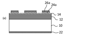
- FIG. 1 is a schematic cross-sectional view showing an example of the substrate 100 with a multilayer reflective film of the present embodiment.
- the substrate 100 with a multilayer reflective film shown in FIG. 1 includes a substrate 10 and a multilayer reflective film 12 formed on the substrate 10.
- a protective film 14 may be formed on the multilayer reflective film 12.
- a back surface conductive film 22 for an electrostatic chuck may be formed on the back surface of the substrate 10 (the surface opposite to the side on which the multilayer reflective film 12 is formed).
- the substrate or film includes not only the case of contacting the upper surface of the substrate or film but also the case of not contacting the upper surface of the substrate or film. That is, “on” the substrate or film includes the case where a new film is formed above the substrate or film, or the case where another film is interposed between the substrate or film. .. Further, “on” does not necessarily mean the upper side in the vertical direction. “On” merely indicates the relative positional relationship between the substrate and the film.
- the substrate 10 preferably has a low coefficient of thermal expansion within the range of 0 ⁇ 5 ppb / ° C. in order to prevent distortion of the transfer pattern due to heat during exposure to EUV light.
- a material having a low coefficient of thermal expansion in this range for example, SiO 2 -TIO 2 -based glass, multi-component glass ceramics, or the like can be used.
- the main surface on the side where the transfer pattern (absorbent pattern described later) of the substrate 10 is formed is processed in order to increase the flatness.
- the flatness is preferably 0.1 ⁇ m or less, more preferably 0.05 ⁇ m or less, and particularly preferably 0.05 ⁇ m or less in the region of 132 mm ⁇ 132 mm on the main surface on the side where the transfer pattern of the substrate 10 is formed. It is preferably 0.03 ⁇ m or less.
- the main surface (back surface) on the side opposite to the side on which the transfer pattern is formed is a surface fixed to the exposure apparatus by an electrostatic chuck.
- the flatness is 0.1 ⁇ m or less, more preferably 0.05 ⁇ m or less, and particularly preferably 0.03 ⁇ m or less.
- the flatness is a value representing a surface warp (deformation amount) represented by TIR (Total Integrated Reading).
- TIR Total Integrated Reading
- the plane determined by the minimum square method with respect to the substrate surface is the focal plane, and the highest position of the substrate surface above the focal plane and the surface of the substrate below the focal plane. It is the absolute value of the height difference from the lowest position.
- the surface roughness of the main surface of the substrate 10 on the side where the transfer pattern is formed is preferably 0.1 nm or less in terms of root mean square roughness (Rq).
- the surface roughness can be measured with an atomic force microscope.
- the substrate 10 preferably has high rigidity in order to prevent deformation of the film (multilayer reflective film 12 or the like) formed on the substrate 10 due to film stress.
- those having a high Young's modulus of 65 GPa or more are preferable.
- the multilayer reflective film 12 has a structure in which a plurality of layers containing elements having different refractive indexes as main components are periodically laminated.
- the multilayer reflective film 12 has a thin film (high refractive index layer) of a light element or a compound thereof which is a high refractive index material and a thin film (low refractive index layer) of a heavy element or a compound thereof which is a low refractive index material. It is composed of a multilayer film in which and are alternately laminated for about 40 to 60 cycles.
- the high refractive index layer and the low refractive index layer may be laminated in this order for a plurality of cycles from the substrate 10 side. In this case, the laminated structure of one (high refractive index layer / low refractive index layer) has one cycle.
- the uppermost layer of the multilayer reflective film 12, that is, the surface layer of the multilayer reflective film 12 on the opposite side of the substrate 10 is preferably a high refractive index layer.
- the high refractive index layer and the low refractive index layer are laminated in this order from the substrate 10 side, the uppermost layer becomes the low refractive index layer.
- the low refractive index layer is the surface of the multilayer reflective film 12
- the low refractive index layer is easily oxidized, and the reflectance of the surface of the multilayer reflective film is reduced. Therefore, it is preferable to form a high refractive index layer on the low refractive index layer.
- the uppermost layer becomes the high refractive index layer.
- the uppermost high-refractive index layer becomes the surface of the multilayer reflective film 12.
- the high refractive index layer contained in the multilayer reflective film 12 is a layer made of a material containing Si.
- the high refractive index layer may contain Si alone or a Si compound.
- the Si compound may contain Si and at least one element selected from the group consisting of B, C, N, O and H.
- the low refractive index layer contained in the multilayer reflective film 12 is a layer made of a material containing a transition metal.
- the transition metal contained in the low refractive index layer is preferably at least one transition metal selected from the group consisting of Mo, Ru, Rh, and Pt.
- the low refractive index layer is more preferably a layer made of a material containing Mo.
- the multilayer reflective film 12 for EUV light having a wavelength of 13 to 14 nm a Mo / Si multilayer film in which Mo films and Si films are alternately laminated for about 40 to 60 cycles can be preferably used.
- the reflectance of such a multilayer reflective film 12 alone is, for example, 65% or more.
- the upper limit of the reflectance of the multilayer reflective film 12 is, for example, 73%.
- the thickness and period of the layers included in the multilayer reflective film 12 can be selected so as to satisfy Bragg's law.
- the multilayer reflective film 12 can be formed by a known method.
- the multilayer reflective film 12 can be formed by, for example, an ion beam sputtering method.
- the multilayer reflective film 12 is a Mo / Si multilayer film
- a Mo film having a thickness of about 3 nm is formed on the substrate 10 by using an ion beam sputtering method using a Mo target.
- a Si film having a thickness of about 4 nm is formed using a Si target.
- the surface layer of the multilayer reflective film 12 on the opposite side of the substrate 10 is a layer containing Si (Si film).
- the thickness of the Mo / Si film in one cycle is 7 nm.
- the outermost peripheral portion of the multilayer reflective film 12 contains a compound containing Si contained in the high refractive index layer and a transition metal contained in the low refractive index layer.
- the ratio of the Si content (atomic%) to the total content (atomic%) of Si and the transition metal is 0.50 or less, preferably 0.45 or less, more preferably 0.45 or less. It is 0.40 or less.
- the ratio of the Si content (atomic%) to the total content (atomic%) of Si and the transition metal is preferably 0.10 or more.
- the compressive stress in the compound is reduced, so that the multilayer reflective film can be used in the mask manufacturing process and cleaning during use of the mask. It is possible to prevent the film from peeling off. As a result, it is possible to reduce the occurrence of defects on the multilayer reflective film or on the absorber film due to the film peeling of the multilayer reflective film. It should be noted that it is not necessary that all the regions in the compound satisfy the above conditions, and the cases where the above conditions are satisfied in at least a part of the regions in the compound are also included in the scope of the present invention.
- the compound contained in the outermost peripheral portion of the multilayer reflective film 12 preferably further contains oxygen.
- the compound contains oxygen the chemical resistance at the outermost peripheral portion of the multilayer reflective film 12 is improved.
- the reflectance of the outermost peripheral portion of the multilayer reflective film 12 which does not contribute to pattern transfer to the exposure light (EUV light) can be reduced, the pattern transfer accuracy at the time of exposure can be further improved. Become.
- the content of oxygen in the compound contained in the outermost peripheral portion of the multilayer reflective film 12 is preferably 0.5 atomic% or more and 75 atomic% or less, and more preferably 5 atomic% or more and 60 atomic% or less. It is more preferably 5 atomic% or more and 40 atomic% or less.
- the compound contained in the outermost peripheral portion of the multilayer reflective film 12 temporarily removes the substrate with the multilayer reflective film from the chamber into the atmosphere after the film formation of the multilayer reflective film 12, and protects the substrate discontinuously from the film formation of the multilayer reflective film 12.
- Oxygen can be contained by forming the film 14. Further, the oxygen content in the compound can be adjusted by adjusting the conditions of cleaning and heat treatment of the substrate with the multilayer reflective film.
- the outermost peripheral portion of the multilayer reflective film 12 is metal silicide (specifically). Is formed of molybdenum silicide). Molybdenum is eluted with sulfuric acid used for SPM cleaning, but metal silicide (specifically, molybdenum silicide) is difficult to elute with sulfuric acid. Therefore, since the chemical resistance during the mask blank manufacturing process, the mask manufacturing process, and the use of the mask is improved, it is possible to prevent the occurrence of film peeling due to the elution of the multilayer reflective film 12. As a result, it is possible to reduce the occurrence of defects on the multilayer reflective film or the absorber film due to the film peeling of the multilayer reflective film 12.
- the outermost peripheral portion of the multilayer reflective film 12 is preferably a range within 20 mm, more preferably within 10 mm, from the end portion on the outermost peripheral side of the multilayer reflective film 12 toward the inside. It is more preferably in the range of 6 mm or less.
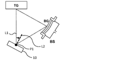
- the ratio of Si and the transition metal in the compound contained in the outermost peripheral portion of the multilayer reflective film 12 is adjusted by, for example, the incident angle and energy of the spatter particles when forming the high refractive index layer and the low refractive index layer. Is possible.
- the incident angle and energy of the spatter particles when forming the high refractive index layer and the low refractive index layer are adjusted by the angle of the substrate and the angle of the sputter target when forming the high refractive index layer and the low refractive index layer. It is possible.
- the "board angle” means the angle formed by the straight line L1 and the straight line L2 in FIG. 7.
- the straight line L1 is a straight line connecting the center P1 of the main surface of the substrate 10 and the center of the surface of the sputtering target TG.
- the straight line L2 is a straight line (normal line) perpendicular to the main surface of the substrate 10 passing through the center P1 of the main surface of the substrate 10. In FIG. 7, the direction in which the substrate 10 is rotated clockwise is defined as a positive angle.
- the "sputter target angle” means the angle formed by the straight line L3 and the straight line L4 in FIG.
- the straight line L3 is a straight line connecting the center P2 on the surface of the sputter target TG and the center of the surface of the beam grid BG of the ion beam source BS.
- the straight line L4 is a straight line (normal line) perpendicular to the surface of the sputter target TG, passing through the center P2 of the surface of the sputter target TG.
- the direction in which the sputter target TG is rotated clockwise is set as a positive angle.
- the ratio of Si and transition metal in the compound contained in the outermost peripheral portion of the multilayer reflective film 12 can be adjusted by the angle of the substrate and the angle of the sputter target. More specifically, the angle of the substrate when forming the low refractive index layer is preferably 20 degrees or more and 45 degrees or less, and the angle of the sputtering target is preferably 45 degrees or more and 65 degrees or less. .. The angle of the substrate for forming the high refractive index layer is preferably 20 degrees or more and 45 degrees or less, and the angle of the sputtering target is preferably 45 degrees or more and 65 degrees or less.
- the substrate 100 with a multilayer reflective film of the present embodiment may have a protective film 14 on the multilayer reflective film 12.
- the protective film 14 has a function of protecting the multilayer reflective film 12 from dry etching and cleaning in the manufacturing process of the reflective mask 200 described later. Further, the protective film 14 also has a function of protecting the multilayer reflective film 12 when the black defect of the transfer pattern is corrected by using the electron beam (EB).
- EB electron beam
- the protective film 14 can be formed by a known method. Examples of the film forming method of the protective film 14 include an ion beam sputtering method, a magnetron sputtering method, a reactive sputtering method, a vapor deposition method (CVD), and a vacuum vapor deposition method.
- the protective film 14 may be continuously formed by an ion beam sputtering method after the film formation of the multilayer reflective film 12.
- the protective film 14 can be formed of a material having different etching selectivity from the absorber film 24 described later.
- the material of the protective film 14 include Ru, Ru- (Nb, Rh, Zr, Y, B, Ti, La, Mo), Si- (Ru, Rh, Cr, B), Rh, Si, Zr, Materials such as Nb, La, and B can be used.
- Ru ruthenium
- it is preferably Ru, Ru- (Nb, Rh, Zr, Y, B, Ti, La, Mo).
- Such a protective film 14 is particularly effective when the absorber film 24 is used as a Ta-based material and the absorber film 24 is patterned by dry etching of a Cl-based gas.
- FIG. 2 is a schematic cross-sectional view showing an example of the reflective mask blank 110 of the present embodiment.
- the reflective mask blank 110 shown in FIG. 2 has an absorber film 24 for absorbing EUV light on the protective film 14 of the substrate 100 with the multilayer reflective film described above.
- the reflective mask blank 110 may further have another thin film such as a resist film 26 on the absorber film 24.
- FIG. 3 is a schematic cross-sectional view showing another example of the reflective mask blank 110 of the present embodiment.
- the reflective mask blank 110 may further have an etching mask film 28 between the absorber film 24 and the resist film 26.
- the resist film 26 on the peripheral edge of the substrate on which the mask pattern is not formed is usually removed (edge rinse).
- edge rinse When the peripheral edge of the resist film 26 is removed, the absorber film 24 beneath it is exposed. In the mask manufacturing process, the exposed absorber film 24 is removed by etching, so that the multilayer reflective film 12 under the absorber film 24 is exposed.
- the multilayer reflective film 12 When the multilayer reflective film 12 is exposed, the multilayer reflective film 12 may be damaged by the mask manufacturing process, cleaning at the time of using the mask, and the like. Therefore, it is preferable that the end portion of the outer periphery of the resist film 26 after being removed by the edge rinse is located above the outermost peripheral portion of the multilayer reflective film 12. According to such a configuration, it is possible to more effectively prevent the multilayer reflective film 12 from being damaged and the film peeling from occurring due to the mask manufacturing process, cleaning at the time of using the mask, and the like.
- the absorber film 24 of the reflective mask blank 110 of the present embodiment is formed on the protective film 14.
- the basic function of the absorber membrane 24 is to absorb EUV light.
- the absorber film 24 may be an absorber film 24 for the purpose of absorbing EUV light, or may be an absorber film 24 having a phase shift function in consideration of the phase difference of EUV light.
- the absorber film 24 having a phase shift function absorbs EUV light and reflects a part of the EUV light to shift the phase. That is, in the reflective mask 200 in which the absorber film 24 having a phase shift function is patterned, the portion where the absorber film 24 is formed absorbs EUV light and dims, and the pattern transfer is not adversely affected. Reflects some light.
- the absorber film 24 having a phase shift function is preferably formed so that the phase difference between the reflected light from the absorber film 24 and the reflected light from the multilayer reflective film 12 is 170 degrees to 260 degrees.
- the image contrast of the projected optical image is improved by the light having the inverted phase difference in the vicinity of 180 degrees interfering with each other at the pattern edge portion. As the image contrast is improved, the resolution is increased, and various exposure-related margins such as exposure amount margin and focal margin can be increased.
- the absorber membrane 24 may be a single-layer membrane or a multilayer membrane composed of a plurality of membranes (for example, a lower absorber membrane and an upper absorber membrane).
- a single-layer film the number of steps during mask blank manufacturing can be reduced and production efficiency is improved.
- its optical constant and film thickness can be appropriately set so that the upper absorber film becomes an antireflection film at the time of mask pattern defect inspection using light. This improves the inspection sensitivity at the time of mask pattern defect inspection using light.
- a membrane to which oxygen (O), nitrogen (N) or the like for improving oxidation resistance is added to the upper absorber membrane is used, the stability over time is improved.
- the absorber membrane 24 By making the absorber membrane 24 a multilayer film in this way, it is possible to add various functions to the absorber membrane 24.
- the absorber film 24 has a phase shift function, the range of adjustment on the optical surface can be increased by forming the multilayer film, so that it becomes easy to obtain a desired reflectance.
- the material of the absorber film 24 has a function of absorbing EUV light and can be processed by etching or the like (preferably, it can be etched by dry etching of chlorine (Cl) -based gas and / or fluorine (F) -based gas).
- the material is not particularly limited as long as it is a material having a high etching selectivity with respect to the protective film 14. Those having such a function include palladium (Pd), silver (Ag), platinum (Pt), gold (Au), iridium (Ir), tungsten (W), chromium (Cr), cobalt (Co), and manganese.
- Mn tin
- Sn tantalum
- Ta vanadium
- V nickel
- Hf hafnium
- Fe iron
- Cu tellurium
- Zn magnesium
- Mg germanium
- Al aluminum
- Rh rhodium
- Ru ruthenium
- Mo molybdenum
- Nb niobium
- Ti titanium
- Zr zirconium
- Y ittrium
- At least one metal selected from silicon (Si), or compounds thereof, can be preferably used.
- the absorber membrane 24 can be formed by a magnetron sputtering method such as a DC sputtering method and an RF sputtering method.
- the absorber film 24 such as a tantalum compound can be formed by a reactive sputtering method using a target containing tantalum and boron and using argon gas to which oxygen or nitrogen is added.
- the tantalum compound for forming the absorber membrane 24 contains an alloy of Ta and the above-mentioned metal.
- the crystalline state of the absorber membrane 24 is preferably an amorphous or microcrystalline structure from the viewpoint of smoothness and flatness.
- the surface of the absorber film 24 is not smooth or flat, the edge roughness of the absorber pattern 24a becomes large, and the dimensional accuracy of the pattern may deteriorate.
- the surface roughness of the absorber film 24 is preferably a root mean square roughness (Rms) of 0.5 nm or less, more preferably 0.4 nm or less, still more preferably 0.3 nm or less.
- Examples of the tantalum compound for forming the absorber film 24 include a compound containing Ta and B, a compound containing Ta and N, a compound containing Ta, O and N, Ta and B, and further O. Compounds containing at least one of and N, compounds containing Ta and Si, compounds containing Ta, Si and N, compounds containing Ta and Ge, compounds containing Ta, Ge and N, and the like. be able to.
- Ta is a material that has a large EUV light absorption coefficient and can be easily dry-etched with a chlorine-based gas or a fluorine-based gas. Therefore, it can be said that Ta is a material for the absorber membrane 24 having excellent processability. Further, by adding B, Si and / or Ge or the like to Ta, an amorphous material can be easily obtained. As a result, the smoothness of the absorber membrane 24 can be improved. Further, if N and / or O is added to Ta, the resistance of the absorber membrane 24 to oxidation is improved, so that the stability over time can be improved.
- An etching mask film 28 may be formed on the absorber film 24.
- the material of the etching mask film 28 it is preferable to use a material having a high etching selectivity of the absorber film 24 with respect to the etching mask film 28.
- the etching selectivity of the absorber film 24 with respect to the etching mask film 28 is preferably 1.5 or more, and more preferably 3 or more.
- the reflective mask blank 110 of the present embodiment preferably has an etching mask film 28 containing chromium (Cr) on the absorber film 24. It is preferable to use chromium or a chromium compound as the material of the etching mask film 28.
- chromium compounds include materials containing Cr and at least one element selected from N, O, C and H.
- the etching mask film 28 more preferably contains CrN, CrO, CrC, CrON, CrOC, CrCN or CrOCN, and is a CrO-based film (CrO film, CrON film, CrOC film or CrOCN film) containing chromium and oxygen. Is more preferable.
- tantalum or a tantalum compound as the material of the etching mask film 28.
- tantalum compounds include materials containing Ta and at least one element selected from N, O, B and H. It is more preferable that the etching mask film 28 contains TaN, TaO, TaON, TaBN, TaBO or TaBON.
- silicon or a silicon compound as the material of the etching mask film 28.
- silicon compounds include materials containing Si and at least one element selected from N, O, C and H, metallic silicon (metal silicide) containing metal in silicon and silicon compounds, and metallic silicon compounds (metals). Silicide compounds) and the like.
- the metal-silicon compound include a material containing a metal, Si, and at least one element selected from N, O, C, and H.
- the film thickness of the etching mask film 28 is preferably 3 nm or more in order to form the pattern on the absorber film 24 with high accuracy.
- the film thickness of the etching mask film 28 is preferably 15 nm or less in order to reduce the film thickness of the resist film 26.
- the back surface conductive film 22 for the electrostatic chuck may be formed on the back surface of the substrate 100 (the surface opposite to the side on which the multilayer reflective film 12 is formed).
- the sheet resistance required for the back surface conductive film 22 for an electrostatic chuck is usually 100 ⁇ / ⁇ ( ⁇ / square) or less.
- the back surface conductive film 22 can be formed by, for example, a magnetron sputtering method or an ion beam sputtering method using a metal such as chromium or tantalum, or a target of an alloy thereof.
- the material of the back surface conductive film 22 is preferably a material containing chromium (Cr) or tantalum (Ta).
- the material of the back surface conductive film 22 is preferably a Cr compound containing at least one selected from boron, nitrogen, oxygen, and carbon in Cr.
- the Cr compound include CrN, CrON, CrCN, CrCON, CrBN, CrBON, CrBCN and CrBOCN.
- the material of the back surface conductive film 22 is preferably Ta (tantalum), an alloy containing Ta, or a Ta compound containing at least one of boron, nitrogen, oxygen, and carbon in any of these.
- Ta compound examples include TaB, TaN, TaO, TaON, TaCON, TaBN, TaBO, TaBON, TaBCON, TaHf, TaHfO, TaHfN, TaHfON, TaHfCON, TaSi, TaSiO, TaSiN, TaSiN, and TaSiN. can.
- the film thickness of the back surface conductive film 22 is not particularly limited as long as it functions as a film for an electrostatic chuck, but is, for example, 10 nm to 200 nm.
- the reflective mask blank 110 of the present embodiment can be used to manufacture the reflective mask 200 of the present embodiment.
- an example of a method for manufacturing a reflective mask will be described.
- FIGS. 4a-f is a schematic diagram showing an example of a method for manufacturing the reflective mask 200.
- the substrate 10, the multilayer reflective film 12 formed on the surface of the substrate 10, the protective film 14 formed on the multilayer reflective film 12, and the protective film 14 are topped.
- a reflective mask blank 110 having an absorber film 24 formed on the surface of the substrate 10 and a back surface conductive film 22 formed on the back surface of the substrate 10 is prepared (FIG. 4a).
- a resist film 26 is formed on the absorber film 24 (FIG. 4b).
- the resist film 26 on the peripheral portion 27 of the substrate is removed with a solvent in which the resist film 26 dissolves (edge rinse) (FIG. 4c).
- a pattern is drawn on the resist film 26 by an electron beam drawing apparatus, and a resist pattern 26a is formed by further undergoing a development / rinsing step (FIG. 4d).
- etching gas of the absorber film 24 for example, a fluorine-based gas and / or a chlorine-based gas can be used.
- Fluorine-based gases include CF 4 , CHF 3 , C2F 6 , C 3 F 6 , C 4 F 6 , C 4 F 8 , CH 2 F 2 , CH 3 F, C 3 F 8 , SF 6 and F 2 .
- Etc. can be used.
- Cl 2 , SiCl 4 , CHCl 3 , CCl 4 , BCl 3 , and the like can be used.
- a mixed gas containing a fluorine-based gas and / or a chlorine-based gas and O 2 in a predetermined ratio can be used.
- These etching gases may further contain an inert gas such as He and / or Ar, if desired.
- the resist pattern 26a is removed with a resist stripping solution.
- the reflective mask 200 of the present embodiment is obtained by undergoing a wet cleaning step using an acidic or alkaline aqueous solution (FIG. 4f).
- a pattern is formed on the etching mask film 28 by using the resist pattern 26a as a mask. After that, a step of forming a pattern on the absorber film 24 using the etching mask pattern as a mask is added.
- the reflective mask 200 thus obtained has a structure in which a multilayer reflective film 12, a protective film 14, and an absorber pattern 24a are laminated on a substrate 10.
- the region 30 where the multilayer reflective film 12 (including the protective film 14) is exposed has a function of reflecting EUV light.
- the region 32 in which the multilayer reflective film 12 (including the protective film 14) is covered with the absorber pattern 24a has a function of absorbing EUV light.
- the thickness of the absorber pattern 24a having a reflectance of, for example, 2.5% or less can be made thinner than before, so that a finer pattern can be transferred. Can be transferred to.
- a transfer pattern can be formed on the semiconductor substrate by lithography using the reflective mask 200 of the present embodiment. This transfer pattern has a shape in which the pattern of the reflective mask 200 is transferred.
- a semiconductor device can be manufactured by forming a transfer pattern on a semiconductor substrate with a reflective mask 200.
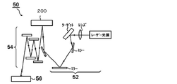
- FIG. 5 shows the pattern transfer device 50.
- the pattern transfer device 50 includes a laser plasma X-ray source 52, a reflective mask 200, a reduction optical system 54, and the like.
- An X-ray reflection mirror is used as the reduction optical system 54.
- the pattern reflected by the reflective mask 200 is usually reduced to about 1/4 by the reduction optical system 54.
- a wavelength band of 13 to 14 nm is used as the exposure wavelength, and the optical path is preset so as to be in a vacuum.
- the EUV light generated by the laser plasma X-ray source 52 is incident on the reflective mask 200.
- the light reflected by the reflective mask 200 is transferred onto the resisted semiconductor substrate 56 via the reduction optical system 54.
- the light reflected by the reflective mask 200 is incident on the reduced optical system 54.
- the light incident on the reduction optical system 54 forms a transfer pattern on the resist film on the resist-attached semiconductor substrate 56.
- a resist pattern can be formed on the resist-attached semiconductor substrate 56.
- etching the semiconductor substrate 56 using the resist pattern as a mask for example, a predetermined wiring pattern can be formed on the semiconductor substrate.
- a semiconductor device can be manufactured by going through such a step and other necessary steps.
- a 6025 size (about 152 mm ⁇ 152 mm ⁇ 6.35 mm) substrate 10 having a polished main surface was prepared.
- the substrate 10 is a substrate made of low thermal expansion glass (SiO 2 -TiO 2 glass).
- the main surface of the substrate 10 was polished by a rough polishing process, a precision polishing process, a local processing process, and a touch polishing process.
- the multilayer reflective film 12 was formed on the main surface of the substrate 10.
- the multilayer reflective film 12 formed on the substrate 10 is a periodic multilayer reflective film 12 composed of Mo and Si in order to obtain a multilayer reflective film 12 suitable for EUV light having a wavelength of 13.5 nm.
- the multilayer reflective film 12 was formed by alternately laminating Mo film and Si film on the substrate 10 by an ion beam sputtering method using a Mo target and a Si target and using krypton (Kr) as a process gas. First, a Si film was formed with a thickness of 4.2 nm, and then a Mo film was formed with a thickness of 2.8 nm.
- the outermost peripheral portion of the multilayer reflective film 12 was irradiated with laser light.
- a CO 2 laser (CW, wavelength 10.6 ⁇ m, output 3 W) was used for irradiating the laser beam.
- the laser beam was irradiated under the condition that the irradiation time was 300 ms.
- the laser beam was irradiated within a range of 6 mm from the outermost peripheral end of the multilayer reflective film 12.
- a Ru protective film 14 (thickness 2.5 nm) was continuously formed on the multilayer reflective film 12 by an ion beam sputtering method after the film was formed on the multilayer reflective film 12.
- the incident angle of the Ru sputtered particles with respect to the normal of the main surface of the substrate 10 was set to 40 degrees, and the gas flow rate of the ion source was set to 8 sccm.
- the substrate with the multilayer reflective film is once taken out from the chamber into the atmosphere, and the Ru protective film 14 is formed discontinuously from the film formation of the multilayer reflective film 12. did.
- the Ru protective film 14 was formed into a film with a film thickness of 2.5 nm by a DC magnetron sputtering method using a Ru target in an Ar gas atmosphere.
- the substrates 100 with the multilayer reflective film of Examples 1 to 5 and Comparative Example 1 were produced.
- the reflective mask blank 110 was manufactured using the above-mentioned substrate 100 with a multilayer reflective film.
- a method for manufacturing the reflective mask blank 110 will be described.
- the absorber film 24 was formed on the protective film 14 of the substrate 100 with a multilayer reflective film by the DC magnetron sputtering method.
- the absorber film 24 was a laminated film 24 composed of two layers, a TaN film which is an absorption layer and a TaO film which is a low reflection layer.
- a TaN film was formed as an absorption layer on the surface of the protective film 14 of the substrate 100 with a multilayer reflective film described above by a DC magnetron sputtering method.
- This TaN film was formed by a reactive sputtering method in a mixed gas atmosphere of Ar gas and N 2 gas in which a substrate 100 with a multilayer reflective film was opposed to a Ta target.
- a TaO film (low reflection layer) was formed on the TaN film by the DC magnetron sputtering method. Similar to the TaN film, this TaO film was formed by a reactive sputtering method in a mixed gas atmosphere of Ar and O 2 in which a substrate 100 with a multilayer reflective film was opposed to a Ta target.
- a back surface conductive film 22 made of CrN was formed on the back surface of the substrate 10 by a magnetron sputtering method (reactive sputtering method) under the following conditions.
- Conditions for forming the back surface conductive film 22 Cr target, mixed gas atmosphere of Ar and N 2 (Ar: 90 atomic%, N: 10 atomic%), film thickness 20 nm.
- the absorber film 24 and the back surface conductive film 22 When forming the absorber film 24 and the back surface conductive film 22 described above, a part of the outer peripheral portion of the substrate 10 is shielded so that the absorber film 24 and the back surface conductive film 22 do not wrap around the end surface of the substrate 10. Then, the absorber film 24 and the back surface conductive film 22 were formed.
- the reflective mask blanks 110 of Examples 1 to 5 and Comparative Example 1 were produced.
- FIG. 6 is a schematic view of an enlarged cross section of the outermost peripheral portion 60 of the multilayer reflective film 12 of the reflective mask blank 110.
- the interface between the Mo layer and the Si layer disappeared.
- a compound made of molybdenum silicide was formed in the outermost peripheral portion 60 of the multilayer reflective film 12.
- the thickness of the outermost peripheral portion 60 of the multilayer reflective film 12 gradually decreased from the center of the substrate 10 toward the outside.
- composition of the outermost peripheral portion 60 of the multilayer reflective film 12 was analyzed by TEM-EDX for the reflective mask blanks 110 of Examples 1 to 5 and Comparative Example 1, and the results were as shown in Table 2 below.
- the reflective mask blanks 110 of Examples 1 to 5 and Comparative Example 1 were washed with SPM.
- a defect inspection was performed on a region of 132 mm ⁇ 132 mm on the surface of the above. As a result, no defect was detected in the reflective mask blanks 110 of Examples 1 to 5 and Comparative Example 1.
- the resist film 26 was formed on the absorber film 24 in the reflective mask blanks 110 of Examples 1 to 5 and Comparative Example 1. Then, the resist film 26 on the peripheral edge of the substrate was removed with a solvent in which the resist film 26 was dissolved to prepare a reflective mask blank from which the resist film 26 on the peripheral edge of the substrate was removed.
- the absorber film 24 was removed by etching using the resist film 24 as a mask. Specifically, the resist film 24 was used as a mask, and the exposed region of the absorber film 24 was removed by etching.
- the reflective mask blanks of Examples 1 to 5 and Comparative Example 1 after cleaning are absorbed by using a high-sensitivity defect inspection device (“MAGICS series” manufactured by Lasertec) having an inspection light source wavelength of 355 nm. Defect inspection was performed on a region of 132 mm ⁇ 132 mm on the surface of the body membrane 24.
- MAGICS series manufactured by Lasertec
- the number of defects detected was 2 in the reflective mask blank 110 of Example 1.
- the number of defects detected was 0.
- the number of defects detected was 20.
- the reason for such a result is that in the reflective mask blank 110 of Comparative Example 1, the Si content of the outermost peripheral portion 60 of the multilayer reflective film 12 was high. That is, it is considered that the cause is that the silicide film having a high Si content has a high compressive stress, so that the film peeling of the multilayer reflective film and more defects on the absorber film due to the film peeling occur.
- the reflective mask blanks 110 of Examples 1 to 5 since the Si content of the outermost peripheral portion 60 of the multilayer reflective film 12 was low, the compressive stress of the outermost peripheral portion 60 was low, and the multilayer reflection was performed. It is considered that the generation of defects on the absorber film 24 due to the peeling of the film 12 could be reduced.
- the reflective mask 200 is manufactured using the reflective mask blanks 110 of Examples 1 to 5, on the multilayer reflective film caused by the film peeling of the multilayer reflective film 12 due to the mask manufacturing process and cleaning during use of the mask. Alternatively, the occurrence of defects on the absorber membrane can be reduced.
- the film peeling of the multilayer reflective film occurs due to the mask manufacturing process or cleaning when the mask is used, and the defect on the multilayer reflective film or the absorber film due to the film peeling of the multilayer reflective film occurs. Is thought to occur frequently.
- the reflective mask blanks 110 of Examples 1 to 5 and Comparative Example 1 were prepared.
- the resist film 26 was formed on the absorber film 24 in the reflective mask blank 110, and then the resist film 26 on the peripheral edge of the substrate was removed.
- a pattern was drawn and developed on the resist film 26 by an electron beam drawing apparatus to form a resist pattern 20a.
- the absorber film 24 was dry-etched using the resist pattern 20a as a mask to form the absorber pattern 24a.
- the reflective mask 200 was manufactured as described above.
- the reflective mask 200 thus obtained was mask-cleaned by SPM cleaning.
- the reflective mask 200 was inspected for defects using a high-sensitivity defect inspection device capable of detecting defects of 21.5 nm with a spherical equivalent diameter SEVD (Sphere Equivalent Volume Diameter). No defects due to film peeling of the multilayer reflective film 12 were detected on the multilayer reflective film 12 of the reflective mask 200 and on the absorber pattern 24a.
- SEVD Sphere Equivalent Volume Diameter
- Substrate 12 Multilayer reflective film 14
- Protective film 22 Backside conductive film 24
- Absorber film 26 Resist film 28
- Etching mask film 60 Outer peripheral part 100
- Substrate with multilayer reflective film 110 Reflective mask blank 200 Reflective mask
Landscapes
- Physics & Mathematics (AREA)
- General Physics & Mathematics (AREA)
- Preparing Plates And Mask In Photomechanical Process (AREA)
- Exposure Of Semiconductors, Excluding Electron Or Ion Beam Exposure (AREA)
Abstract
Provided are a multilayer reflective film-equipped substrate, a reflective mask blank, a reflective mask manufacturing method, and a semiconductor device manufacturing method that prevent a multilayer reflective film from peeling due to a mask manufacturing step, cleaning when using a mask, or the like, and are capable of reducing defects that occur in an absorber film caused by the peeling of a multilayer reflective film. The multilayer reflective film-equipped substrate 10 includes a substrate 10 and a multilayer reflective film 12 that is formed on the main surface of the substrate 10. The multilayer reflective film 12 has a configuration in which high-refractive-index layers and low-refractive-index layers are stacked alternatingly. The high-refractive-index layers comprise a material that includes Si.
The low-refractive-index layers comprise a material that includes a transition metal. The outermost periphery 60 of the multilayer reflective film 12 comprises a compound that includes Si and a transition metal. The ratio of the Si content rate (at%) to the total content rate (at%) of Si and the transition metal in the compound is 0.50 or less.
Description
本発明は、多層反射膜付き基板、反射型マスクブランク、反射型マスクの製造方法、及び半導体装置の製造方法に関する。
The present invention relates to a substrate with a multilayer reflective film, a reflective mask blank, a method for manufacturing a reflective mask, and a method for manufacturing a semiconductor device.
近年における超LSIデバイスの高密度化、高精度化の更なる要求に伴い、極紫外(Extreme Ultra Violet、以下、EUVと称す)光を用いた露光技術であるEUVリソグラフィが有望視されている。EUV光とは軟X線領域又は真空紫外線領域の波長帯の光を指し、具体的には波長が0.2~100nm程度の光のことである。
With the recent demand for higher density and higher accuracy of VLSI devices, EUV lithography, which is an exposure technology using extreme ultraviolet (Extreme Ultra Violet, hereinafter referred to as EUV) light, is expected to be promising. EUV light refers to light in the wavelength band of the soft X-ray region or the vacuum ultraviolet region, and specifically refers to light having a wavelength of about 0.2 to 100 nm.
反射型マスクは、基板の上に形成された露光光を反射するための多層反射膜と、多層反射膜の上に形成され、露光光を吸収するためのパターン状の吸収体膜である吸収体パターンとを有する。半導体基板上にパターン転写を行うための露光機に搭載された反射型マスクに入射した光は、吸収体パターンのある部分では吸収され、吸収体パターンのない部分では多層反射膜により反射される。多層反射膜により反射された光像が、反射光学系を通してシリコンウエハ等の半導体基板上に転写される。
The reflective mask is an absorber which is a multilayer reflective film formed on a substrate for reflecting the exposure light and a patterned absorber film formed on the multilayer reflective film for absorbing the exposure light. Has a pattern. The light incident on the reflective mask mounted on the exposure machine for pattern transfer on the semiconductor substrate is absorbed in the portion having the absorber pattern and reflected by the multilayer reflective film in the portion without the absorber pattern. The light image reflected by the multilayer reflective film is transferred onto a semiconductor substrate such as a silicon wafer through a reflective optical system.
多層反射膜としては、一般的に、屈折率の異なる元素が周期的に積層された多層膜が用いられる。例えば、波長13~14nmのEUV光に対する多層反射膜としては、Mo膜とSi膜を交互に40周期程度積層したMo/Si周期積層膜が好ましく用いられる。
As the multilayer reflective film, a multilayer film in which elements having different refractive indexes are periodically laminated is generally used. For example, as the multilayer reflective film for EUV light having a wavelength of 13 to 14 nm, a Mo / Si periodic laminated film in which Mo film and Si film are alternately laminated for about 40 cycles is preferably used.
特許文献1には、基板と、基板の表面に形成された多層反射膜と、多層反射膜の上に形成された保護膜と、保護膜の上に形成された吸収膜を備えたEUVリソグラフィ用反射型マスクブランクが記載されている。
Patent Document 1 describes a substrate, a multilayer reflective film formed on the surface of the substrate, a protective film formed on the multilayer reflective film, and an absorbent film formed on the protective film for EUV lithography. A reflective mask blank is described.
反射型マスクブランクは、一般に、基板の一方の主表面に露光光(EUV光)を反射する多層反射膜が形成され、この多層反射膜上に露光光(EUV光)を吸収する吸収体膜が形成された構造を有する。
In a reflective mask blank, a multilayer reflective film that reflects exposure light (EUV light) is generally formed on one main surface of a substrate, and an absorber film that absorbs exposure light (EUV light) is formed on the multilayer reflective film. It has a formed structure.
反射型マスクブランクを用いて反射型マスクを製造する場合、まず反射型マスクブランクの表面に電子線描画用のレジスト膜を形成する。次に、このレジスト膜に対し所望のパターンを電子線で描画し、パターンの現像を行ってレジストパターンを形成する。次いで、このレジストパターンをマスクとして、吸収体膜をドライエッチングして吸収体パターン(転写パターン)を形成する。これにより、多層反射膜上に吸収体パターンが形成された反射型マスクを製造することができる。
When manufacturing a reflective mask using a reflective mask blank, first, a resist film for drawing an electron beam is formed on the surface of the reflective mask blank. Next, a desired pattern is drawn on the resist film with an electron beam, and the pattern is developed to form a resist pattern. Next, using this resist pattern as a mask, the absorber film is dry-etched to form an absorber pattern (transfer pattern). This makes it possible to manufacture a reflective mask in which an absorber pattern is formed on the multilayer reflective film.
近年、反射型マスクの品質に対する要求が高くなっており、従来では問題にならなかった多層反射膜付き基板及び反射型マスクブランクにおける、多層反射膜に起因する欠陥が問題となっている。
In recent years, the demand for the quality of the reflective mask has been increasing, and defects caused by the multilayer reflective film in the substrate with the multilayer reflective film and the reflective mask blank, which have not been a problem in the past, have become a problem.
反射型マスクブランクにおける多層反射膜は、通常、イオンビームスパッタリング装置やマグネトロンスパッタリング装置を用いて基板の主表面上に形成される。多層反射膜は、基板の端面に回り込むように形成されることがある。また、多層反射膜は、基板の端面に回り込まないように形成されることがある。多層反射膜を形成する際に、静電チャック装置を用いて基板を保持した場合には、通常は基板の端面に回り込むように多層反射膜が形成される。一方、多層反射膜を形成する際に、機械的なチャック装置(例えば特開2005-77845号公報に記載のチャック装置)を用いて基板を保持した場合には、基板の主表面の周縁部がチャック装置の上面プレートによって覆われる。そのため、通常は基板の端面に回り込まないように多層反射膜が形成される。そして、上記レジスト膜は反射型マスクブランクの全面に形成される。基板周縁部のレジスト膜の剥離による発塵を抑制するため、通常、マスクパターンが形成されない基板周縁部のレジスト膜を除去すること(エッジリンス)が行われる。
The multilayer reflective film in the reflective mask blank is usually formed on the main surface of the substrate by using an ion beam sputtering device or a magnetron sputtering device. The multilayer reflective film may be formed so as to wrap around the end face of the substrate. Further, the multilayer reflective film may be formed so as not to wrap around the end face of the substrate. When the substrate is held by using an electrostatic chuck device when forming the multilayer reflective film, the multilayer reflective film is usually formed so as to wrap around the end face of the substrate. On the other hand, when the substrate is held by using a mechanical chuck device (for example, the chuck device described in Japanese Patent Application Laid-Open No. 2005-77745) when forming the multilayer reflective film, the peripheral edge of the main surface of the substrate is formed. Covered by the top plate of the chuck device. Therefore, a multilayer reflective film is usually formed so as not to wrap around the end face of the substrate. Then, the resist film is formed on the entire surface of the reflective mask blank. In order to suppress dust generation due to peeling of the resist film on the peripheral edge of the substrate, usually, the resist film on the peripheral edge of the substrate on which the mask pattern is not formed is removed (edge rinse).
このように基板周縁部のレジスト膜が除去された(換言すれば、基板周縁部にはレジスト膜が形成されていない)状態の反射型マスクブランクを用いて上記のように反射型マスクを製造した場合、基板周縁部にはレジスト膜が形成されていない。そのため、露出している吸収体膜がエッチングにより除去されてしまい、吸収体膜の下にある多層反射膜が露出することになる。通常、反射型マスクの製造工程において、吸収体パターンを形成した後に、レジストパターン除去のために酸性やアルカリ性の水溶液(薬液)を用いたウェット洗浄が行われる。また、半導体装置の製造においても、露光時に反射型マスクに付着した異物を除去するため、薬液を用いたウェット洗浄が行われる。これらの洗浄は少なくとも複数回行われる。波長13~14nmのEUV光に対する多層反射膜としては、Mo膜とSi膜を交互に40周期程度積層したMo/Si周期積層膜が好ましく用いられる。この洗浄によって、基板周縁部において露出した多層反射膜が損傷し、膜剥がれが発生することがある。このような多層反射膜の膜剥がれは、重大なパターン欠陥の原因となるおそれがある。
A reflective mask was manufactured as described above using a reflective mask blank in which the resist film on the peripheral edge of the substrate was removed (in other words, no resist film was formed on the peripheral edge of the substrate). In this case, the resist film is not formed on the peripheral edge of the substrate. Therefore, the exposed absorber film is removed by etching, and the multilayer reflective film under the absorber film is exposed. Usually, in the manufacturing process of the reflective mask, after forming the absorber pattern, wet cleaning using an acidic or alkaline aqueous solution (chemical solution) is performed to remove the resist pattern. Also, in the manufacture of semiconductor devices, wet cleaning using a chemical solution is performed in order to remove foreign substances adhering to the reflective mask during exposure. These washes are performed at least multiple times. As the multilayer reflective film for EUV light having a wavelength of 13 to 14 nm, a Mo / Si periodic laminated film in which Mo film and Si film are alternately laminated for about 40 cycles is preferably used. This cleaning may damage the exposed multilayer reflective film at the peripheral edge of the substrate and cause film peeling. Such peeling of the multilayer reflective film may cause serious pattern defects.
上記特許文献1に記載の多層反射膜付き基板及び反射型マスクブランクでは、多層反射膜の外周領域に改質領域を形成している。この改質領域は、多層反射膜を構成する高屈折率層の材料と低屈折率層の材料の化合物によって形成されている。このような改質領域を形成することによって、多層反射膜や吸収体膜の膜剥がれに起因する欠陥発生を低減することができる。高屈折率層の材料としては、ケイ素(Si)を含む材料が用いられる。低屈折率層の材料としては、モリブデン(Mo)を含む材料が用いられている。
In the substrate with a multilayer reflective film and the reflective mask blank described in Patent Document 1, a modified region is formed in the outer peripheral region of the multilayer reflective film. This modified region is formed of a compound of the material of the high refractive index layer and the material of the low refractive index layer constituting the multilayer reflective film. By forming such a modified region, it is possible to reduce the occurrence of defects due to film peeling of the multilayer reflective film and the absorber film. As the material of the high refractive index layer, a material containing silicon (Si) is used. As the material of the low refractive index layer, a material containing molybdenum (Mo) is used.
上記特許文献1に記載の多層反射膜付き基板及び反射型マスクブランクによれば、多層反射膜の外周領域に改質領域を形成しているため、多層反射膜の外周の端部における耐薬品性が向上し、多層反射膜の膜剥がれを低減することができる。しかし、改質領域はSiを含んでおり、Si含有率が高いシリサイド膜は圧縮応力が高いため、多層反射膜の膜剥がれや、膜剥がれに起因する吸収体膜上の欠陥を十分に低減することができないという問題があった。
According to the substrate with the multilayer reflective film and the reflective mask blank described in Patent Document 1, since the modified region is formed in the outer peripheral region of the multilayer reflective film, the chemical resistance at the outer peripheral end of the multilayer reflective film is formed. Can be improved and peeling of the multilayer reflective film can be reduced. However, since the modified region contains Si and the silicide film having a high Si content has a high compressive stress, the film peeling of the multilayer reflective film and the defects on the absorber film due to the film peeling are sufficiently reduced. There was a problem that it could not be done.
本発明は、上述の問題を解決するためになされたものである。本発明は、マスク製造工程及びマスク使用時の洗浄等による多層反射膜の膜剥がれを防止し、多層反射膜の膜剥がれに起因する多層反射膜上、または、吸収体膜上の欠陥発生を低減することのできる多層反射膜付き基板、反射型マスクブランク、反射型マスクの製造方法、及び半導体装置の製造方法を提供することを目的とする。
The present invention has been made to solve the above-mentioned problems. The present invention prevents the film peeling of the multilayer reflective film due to the mask manufacturing process and cleaning when the mask is used, and reduces the generation of defects on the multilayer reflective film or the absorber film due to the film peeling of the multilayer reflective film. It is an object of the present invention to provide a substrate with a multilayer reflective film, a reflective mask blank, a method for manufacturing a reflective mask, and a method for manufacturing a semiconductor device.
上記課題を解決するため、本発明は以下の構成を有する。
In order to solve the above problems, the present invention has the following configurations.
(構成1)
基板と、該基板の主表面上に形成された多層反射膜とを含む多層反射膜付き基板であって、
前記多層反射膜は、高屈折率層と低屈折率層を交互に積層した構造を有し、
前記高屈折率層はSiを含む材料からなり、前記低屈折率層は遷移金属を含む材料からなり、
前記多層反射膜の最外周部は、Siと遷移金属とを含む化合物からなり、
前記化合物におけるSiと遷移金属の合計含有率(原子%)に対するSiの含有率(原子%)の比は、0.50以下であることを特徴とする多層反射膜付き基板。 (Structure 1)
A substrate with a multilayer reflective film including a substrate and a multilayer reflective film formed on the main surface of the substrate.
The multilayer reflective film has a structure in which high refractive index layers and low refractive index layers are alternately laminated.
The high refractive index layer is made of a material containing Si, and the low refractive index layer is made of a material containing a transition metal.
The outermost peripheral portion of the multilayer reflective film is made of a compound containing Si and a transition metal.
A substrate with a multilayer reflective film, wherein the ratio of the Si content (atomic%) to the total content (atomic%) of Si and the transition metal in the compound is 0.50 or less.
(構成2)
前記化合物は酸素を含有することを特徴とする構成1記載の多層反射膜付き基板。 (Structure 2)
The substrate with a multilayer reflective film according to Configuration 1, wherein the compound contains oxygen.
前記化合物は酸素を含有することを特徴とする構成1記載の多層反射膜付き基板。 (Structure 2)
The substrate with a multilayer reflective film according to Configuration 1, wherein the compound contains oxygen.
(構成3)
前記化合物中の前記酸素の含有率は、0.5原子%以上75原子%以下であることを特徴とする構成2記載の多層反射膜付き基板。 (Structure 3)
The substrate with a multilayer reflective film according to Configuration 2, wherein the oxygen content in the compound is 0.5 atomic% or more and 75 atomic% or less.
前記化合物中の前記酸素の含有率は、0.5原子%以上75原子%以下であることを特徴とする構成2記載の多層反射膜付き基板。 (Structure 3)
The substrate with a multilayer reflective film according to Configuration 2, wherein the oxygen content in the compound is 0.5 atomic% or more and 75 atomic% or less.
(構成4)
前記多層反射膜上に、保護膜が形成されていることを特徴とする構成1乃至3の何れか一に記載の多層反射膜付き基板。 (Structure 4)
The substrate with a multilayer reflective film according to any one of configurations 1 to 3, wherein a protective film is formed on the multilayer reflective film.
前記多層反射膜上に、保護膜が形成されていることを特徴とする構成1乃至3の何れか一に記載の多層反射膜付き基板。 (Structure 4)
The substrate with a multilayer reflective film according to any one of configurations 1 to 3, wherein a protective film is formed on the multilayer reflective film.
(構成5)
基板の主表面上に、高屈折率層と低屈折率層を交互に積層した多層反射膜と、吸収体膜とが形成された反射型マスクブランクにおいて、
前記多層反射膜における前記高屈折率層はSiを含む材料からなり、前記低屈折率層は遷移金属を含む材料からなり、
前記主表面上に形成された前記多層反射膜の最外周部は、Siと遷移金属とを含む化合物からなり、
前記化合物におけるSiと遷移金属の合計含有率(原子%)に対するSiの含有率(原子%)の比は、0.50以下であることを特徴とする反射型マスクブランク 。 (Structure 5)
In a reflective mask blank in which a multilayer reflective film in which high refractive index layers and low refractive index layers are alternately laminated on the main surface of a substrate and an absorber film are formed.
The high refractive index layer in the multilayer reflective film is made of a material containing Si, and the low refractive index layer is made of a material containing a transition metal.
The outermost peripheral portion of the multilayer reflective film formed on the main surface is made of a compound containing Si and a transition metal.
A reflective mask blank characterized in that the ratio of the Si content (atomic%) to the total content (atomic%) of Si and the transition metal in the compound is 0.50 or less.
(構成6)
前記化合物は酸素を含有することを特徴とする構成5記載の反射型マスクブランク。 (Structure 6)
The reflective mask blank according to composition 5, wherein the compound contains oxygen.
前記化合物は酸素を含有することを特徴とする構成5記載の反射型マスクブランク。 (Structure 6)
The reflective mask blank according to composition 5, wherein the compound contains oxygen.
(構成7)
前記化合物中の前記酸素の含有率は、0.5原子%以上75原子%以下であることを特徴とする構成6記載の反射型マスクブランク。 (Structure 7)
The reflective mask blank according to composition 6, wherein the oxygen content in the compound is 0.5 atomic% or more and 75 atomic% or less.
前記化合物中の前記酸素の含有率は、0.5原子%以上75原子%以下であることを特徴とする構成6記載の反射型マスクブランク。 (Structure 7)
The reflective mask blank according to composition 6, wherein the oxygen content in the compound is 0.5 atomic% or more and 75 atomic% or less.
(構成8)
前記多層反射膜と前記吸収体膜との間に、前記吸収体膜とエッチング選択性が異なる材料からなる保護膜が形成されていることを特徴とする構成5乃至7の何れか一に記載の反射型マスクブランク。 (Structure 8)
The invention according to any one of configurations 5 to 7, wherein a protective film made of a material having different etching selectivity from the absorber film is formed between the multilayer reflective film and the absorber film. Reflective mask blank.
(構成9)
前記吸収体膜上にレジスト膜が形成されていることを特徴とする構成5乃至8の何れか一に記載の反射型マスクブランク。 (Structure 9)
The reflective mask blank according to any one of configurations 5 to 8, wherein a resist film is formed on the absorber film.
前記吸収体膜上にレジスト膜が形成されていることを特徴とする構成5乃至8の何れか一に記載の反射型マスクブランク。 (Structure 9)
The reflective mask blank according to any one of configurations 5 to 8, wherein a resist film is formed on the absorber film.
(構成10)
前記レジスト膜の外周の端部は、前記化合物からなる前記多層反射膜の最外周部の上方に位置することを特徴とする構成9記載の反射型マスクブランク。 (Structure 10)
The reflective mask blank according to configuration 9, wherein the outer peripheral edge of the resist film is located above the outermost peripheral edge of the multilayer reflective film made of the compound.
前記レジスト膜の外周の端部は、前記化合物からなる前記多層反射膜の最外周部の上方に位置することを特徴とする構成9記載の反射型マスクブランク。 (Structure 10)
The reflective mask blank according to configuration 9, wherein the outer peripheral edge of the resist film is located above the outermost peripheral edge of the multilayer reflective film made of the compound.
(構成11)
構成9または10に記載の反射型マスクブランクを準備し、前記吸収体膜をパターニングして、前記多層反射膜上に吸収体パターンを形成することを特徴とする反射型マスクの製造方法。 (Structure 11)
A method for producing a reflective mask, which comprises preparing the reflective mask blank according to theconfiguration 9 or 10 and patterning the absorber film to form an absorber pattern on the multilayer reflective film.
構成9または10に記載の反射型マスクブランクを準備し、前記吸収体膜をパターニングして、前記多層反射膜上に吸収体パターンを形成することを特徴とする反射型マスクの製造方法。 (Structure 11)
A method for producing a reflective mask, which comprises preparing the reflective mask blank according to the
(構成12)
構成11に記載の反射型マスクの製造方法によって得られた反射型マスクを用い、半導体基板上のレジスト膜に吸収体パターンを転写する工程を有することを特徴とする半導体装置の製造方法。 (Structure 12)
A method for manufacturing a semiconductor device, which comprises a step of transferring an absorber pattern to a resist film on a semiconductor substrate by using the reflective mask obtained by the method for manufacturing a reflective mask according to the configuration 11.
本発明によれば、マスク製造工程及びマスク使用時の洗浄等による多層反射膜の膜剥がれを防止し、多層反射膜の膜剥がれに起因する多層反射膜上、または、吸収体膜上の欠陥発生を低減することのできる多層反射膜付き基板、反射型マスクブランク、反射型マスクの製造方法、及び半導体装置の製造方法を提供することができる。
According to the present invention, the film peeling of the multilayer reflective film is prevented due to the mask manufacturing process and cleaning when the mask is used, and defects are generated on the multilayer reflective film or the absorber film due to the film peeling of the multilayer reflective film. A substrate with a multilayer reflective film, a reflective mask blank, a method for manufacturing a reflective mask, and a method for manufacturing a semiconductor device can be provided.
以下、本発明の実施形態について、図面を参照しながら具体的に説明する。なお、以下の実施形態は、本発明を具体的に説明するための形態であって、本発明をその範囲内に限定するものではない。
Hereinafter, embodiments of the present invention will be specifically described with reference to the drawings. It should be noted that the following embodiments are embodiments for specifically explaining the present invention, and do not limit the present invention to the scope thereof.
図1は、本実施形態の多層反射膜付き基板100の一例を示す断面模式図である。図1に示す多層反射膜付き基板100は、基板10と、基板10の上に形成された多層反射膜12とを含む。多層反射膜12の上には、保護膜14が形成されてもよい。基板10の裏面(多層反射膜12が形成された側と反対側の面)には、静電チャック用の裏面導電膜22が形成されてもよい。
FIG. 1 is a schematic cross-sectional view showing an example of the substrate 100 with a multilayer reflective film of the present embodiment. The substrate 100 with a multilayer reflective film shown in FIG. 1 includes a substrate 10 and a multilayer reflective film 12 formed on the substrate 10. A protective film 14 may be formed on the multilayer reflective film 12. A back surface conductive film 22 for an electrostatic chuck may be formed on the back surface of the substrate 10 (the surface opposite to the side on which the multilayer reflective film 12 is formed).
なお、本明細書において、基板や膜の「上に」とは、その基板や膜の上面に接触する場合だけでなく、その基板や膜の上面に接触しない場合も含む。すなわち、基板や膜の「上に」とは、その基板や膜の上方に新たな膜が形成される場合や、その基板や膜との間に他の膜が介在している場合等を含む。また、「上に」とは、必ずしも鉛直方向における上側を意味するものではない。「上に」とは、基板や膜などの相対的な位置関係を示しているに過ぎない。
In the present specification, "on" the substrate or film includes not only the case of contacting the upper surface of the substrate or film but also the case of not contacting the upper surface of the substrate or film. That is, "on" the substrate or film includes the case where a new film is formed above the substrate or film, or the case where another film is interposed between the substrate or film. .. Further, "on" does not necessarily mean the upper side in the vertical direction. "On" merely indicates the relative positional relationship between the substrate and the film.
<基板>
基板10は、EUV光による露光時の熱による転写パターンの歪みを防止するため、0±5ppb/℃の範囲内の低熱膨張係数を有するものが好ましく用いられる。この範囲の低熱膨張係数を有する素材としては、例えば、SiO2-TiO2系ガラス、多成分系ガラスセラミックス等を用いることができる。 <Board>
Thesubstrate 10 preferably has a low coefficient of thermal expansion within the range of 0 ± 5 ppb / ° C. in order to prevent distortion of the transfer pattern due to heat during exposure to EUV light. As a material having a low coefficient of thermal expansion in this range, for example, SiO 2 -TIO 2 -based glass, multi-component glass ceramics, or the like can be used.
基板10は、EUV光による露光時の熱による転写パターンの歪みを防止するため、0±5ppb/℃の範囲内の低熱膨張係数を有するものが好ましく用いられる。この範囲の低熱膨張係数を有する素材としては、例えば、SiO2-TiO2系ガラス、多成分系ガラスセラミックス等を用いることができる。 <Board>
The
基板10の転写パターン(後述の吸収体パターン)が形成される側の主表面は、平坦度を高めるために加工されることが好ましい。基板10の主表面の平坦度を高めることによって、パターンの位置精度や転写精度を高めることができる。例えば、EUV露光の場合、基板10の転写パターンが形成される側の主表面の132mm×132mmの領域において、平坦度が0.1μm以下であることが好ましく、更に好ましくは0.05μm以下、特に好ましくは0.03μm以下である。また、転写パターンが形成される側と反対側の主表面(裏面)は、露光装置に静電チャックによって固定される面である。裏面の142mm×142mmの領域において、平坦度が0.1μm以下、更に好ましくは0.05μm以下、特に好ましくは0.03μm以下である。なお、本明細書において平坦度は、TIR(Total Indicated Reading)で示される表面の反り(変形量)を表す値である。具体的には、平坦度は、基板表面を基準として最小二乗法で定められる平面を焦平面とし、この焦平面より上にある基板表面の最も高い位置と、焦平面より下にある基板表面の最も低い位置との高低差の絶対値である。
It is preferable that the main surface on the side where the transfer pattern (absorbent pattern described later) of the substrate 10 is formed is processed in order to increase the flatness. By increasing the flatness of the main surface of the substrate 10, the position accuracy and transfer accuracy of the pattern can be improved. For example, in the case of EUV exposure, the flatness is preferably 0.1 μm or less, more preferably 0.05 μm or less, and particularly preferably 0.05 μm or less in the region of 132 mm × 132 mm on the main surface on the side where the transfer pattern of the substrate 10 is formed. It is preferably 0.03 μm or less. Further, the main surface (back surface) on the side opposite to the side on which the transfer pattern is formed is a surface fixed to the exposure apparatus by an electrostatic chuck. In the region of 142 mm × 142 mm on the back surface, the flatness is 0.1 μm or less, more preferably 0.05 μm or less, and particularly preferably 0.03 μm or less. In the present specification, the flatness is a value representing a surface warp (deformation amount) represented by TIR (Total Integrated Reading). Specifically, for the flatness, the plane determined by the minimum square method with respect to the substrate surface is the focal plane, and the highest position of the substrate surface above the focal plane and the surface of the substrate below the focal plane. It is the absolute value of the height difference from the lowest position.
EUV露光の場合、基板10の転写パターンが形成される側の主表面の表面粗さは、二乗平均平方根粗さ(Rq)で0.1nm以下であることが好ましい。なお表面粗さは、原子間力顕微鏡で測定することができる。
In the case of EUV exposure, the surface roughness of the main surface of the substrate 10 on the side where the transfer pattern is formed is preferably 0.1 nm or less in terms of root mean square roughness (Rq). The surface roughness can be measured with an atomic force microscope.
基板10は、その上に形成される膜(多層反射膜12など)の膜応力による変形を防止するために、高い剛性を有しているものが好ましい。特に、65GPa以上の高いヤング率を有しているものが好ましい。
The substrate 10 preferably has high rigidity in order to prevent deformation of the film (multilayer reflective film 12 or the like) formed on the substrate 10 due to film stress. In particular, those having a high Young's modulus of 65 GPa or more are preferable.
<多層反射膜>
多層反射膜12は、屈折率の異なる元素を主成分とする複数の層が周期的に積層された構成を有している。一般的に、多層反射膜12は、高屈折率材料である軽元素又はその化合物の薄膜(高屈折率層)と、低屈折率材料である重元素又はその化合物の薄膜(低屈折率層)とが交互に40~60周期程度積層された多層膜からなる。
多層反射膜12を形成するために、基板10側から高屈折率層と低屈折率層をこの順に複数周期積層してもよい。この場合、1つの(高屈折率層/低屈折率層)の積層構造が、1周期となる。 <Multilayer reflective film>
The multilayerreflective film 12 has a structure in which a plurality of layers containing elements having different refractive indexes as main components are periodically laminated. Generally, the multilayer reflective film 12 has a thin film (high refractive index layer) of a light element or a compound thereof which is a high refractive index material and a thin film (low refractive index layer) of a heavy element or a compound thereof which is a low refractive index material. It is composed of a multilayer film in which and are alternately laminated for about 40 to 60 cycles.
In order to form the multilayerreflective film 12, the high refractive index layer and the low refractive index layer may be laminated in this order for a plurality of cycles from the substrate 10 side. In this case, the laminated structure of one (high refractive index layer / low refractive index layer) has one cycle.
多層反射膜12は、屈折率の異なる元素を主成分とする複数の層が周期的に積層された構成を有している。一般的に、多層反射膜12は、高屈折率材料である軽元素又はその化合物の薄膜(高屈折率層)と、低屈折率材料である重元素又はその化合物の薄膜(低屈折率層)とが交互に40~60周期程度積層された多層膜からなる。
多層反射膜12を形成するために、基板10側から高屈折率層と低屈折率層をこの順に複数周期積層してもよい。この場合、1つの(高屈折率層/低屈折率層)の積層構造が、1周期となる。 <Multilayer reflective film>
The multilayer
In order to form the multilayer
なお、多層反射膜12の最上層、すなわち多層反射膜12の基板10と反対側の表面層は、高屈折率層であることが好ましい。基板10側から高屈折率層と低屈折率層をこの順に積層する場合は、最上層が低屈折率層となる。しかし、低屈折率層が多層反射膜12の表面である場合、低屈折率層が容易に酸化されることで多層反射膜の表面の反射率が減少してしまう。そのため、その低屈折率層の上に高屈折率層を形成することが好ましい。一方、基板10側から低屈折率層と高屈折率層をこの順に積層する場合は、最上層が高屈折率層となる。その場合は、最上層の高屈折率層が、多層反射膜12の表面となる。
The uppermost layer of the multilayer reflective film 12, that is, the surface layer of the multilayer reflective film 12 on the opposite side of the substrate 10 is preferably a high refractive index layer. When the high refractive index layer and the low refractive index layer are laminated in this order from the substrate 10 side, the uppermost layer becomes the low refractive index layer. However, when the low refractive index layer is the surface of the multilayer reflective film 12, the low refractive index layer is easily oxidized, and the reflectance of the surface of the multilayer reflective film is reduced. Therefore, it is preferable to form a high refractive index layer on the low refractive index layer. On the other hand, when the low refractive index layer and the high refractive index layer are laminated in this order from the substrate 10 side, the uppermost layer becomes the high refractive index layer. In that case, the uppermost high-refractive index layer becomes the surface of the multilayer reflective film 12.
多層反射膜12に含まれる高屈折率層は、Siを含む材料からなる層である。高屈折率層は、Si単体を含んでもよく、Si化合物を含んでもよい。Si化合物は、Siと、B、C、N、O及びHからなる群から選択される少なくとも1つの元素を含んでもよい。Siを含む層を高屈折率層として使用することによって、EUV光の反射率に優れた多層反射膜が得られる。
The high refractive index layer contained in the multilayer reflective film 12 is a layer made of a material containing Si. The high refractive index layer may contain Si alone or a Si compound. The Si compound may contain Si and at least one element selected from the group consisting of B, C, N, O and H. By using the layer containing Si as the high refractive index layer, a multilayer reflective film having excellent reflectance of EUV light can be obtained.
多層反射膜12に含まれる低屈折率層は、遷移金属を含む材料からなる層である。低屈折率層に含まれる遷移金属は、Mo、Ru、Rh、及びPtからなる群から選択される少なくとも1つの遷移金属であることが好ましい。低屈折率層は、Moを含む材料からなる層であることがより好ましい。
The low refractive index layer contained in the multilayer reflective film 12 is a layer made of a material containing a transition metal. The transition metal contained in the low refractive index layer is preferably at least one transition metal selected from the group consisting of Mo, Ru, Rh, and Pt. The low refractive index layer is more preferably a layer made of a material containing Mo.
例えば、波長13~14nmのEUV光のための多層反射膜12としては、好ましくは、Mo膜とSi膜を交互に40~60周期程度積層したMo/Si多層膜を用いることができる。
For example, as the multilayer reflective film 12 for EUV light having a wavelength of 13 to 14 nm, a Mo / Si multilayer film in which Mo films and Si films are alternately laminated for about 40 to 60 cycles can be preferably used.
このような多層反射膜12の単独での反射率は、例えば65%以上である。多層反射膜12の反射率の上限は、例えば73%である。なお、多層反射膜12に含まれる層の厚み及び周期は、ブラッグの法則を満たすように選択することができる。
The reflectance of such a multilayer reflective film 12 alone is, for example, 65% or more. The upper limit of the reflectance of the multilayer reflective film 12 is, for example, 73%. The thickness and period of the layers included in the multilayer reflective film 12 can be selected so as to satisfy Bragg's law.
多層反射膜12は、公知の方法によって形成できる。多層反射膜12は、例えば、イオンビームスパッタ法により形成できる。
The multilayer reflective film 12 can be formed by a known method. The multilayer reflective film 12 can be formed by, for example, an ion beam sputtering method.
例えば、多層反射膜12がMo/Si多層膜である場合、イオンビームスパッタ法により、Moターゲットを用いて、厚さ3nm程度のMo膜を基板10の上に形成する。次に、Siターゲットを用いて、厚さ4nm程度のSi膜を形成する。このような操作を繰り返すことによって、Mo/Si膜が40~60周期積層した多層反射膜12を形成することができる。このとき、多層反射膜12の基板10と反対側の表面層は、Siを含む層(Si膜)である。1周期のMo/Si膜の厚みは、7nmとなる。
For example, when the multilayer reflective film 12 is a Mo / Si multilayer film, a Mo film having a thickness of about 3 nm is formed on the substrate 10 by using an ion beam sputtering method using a Mo target. Next, a Si film having a thickness of about 4 nm is formed using a Si target. By repeating such an operation, it is possible to form a multilayer reflective film 12 in which Mo / Si films are laminated for 40 to 60 cycles. At this time, the surface layer of the multilayer reflective film 12 on the opposite side of the substrate 10 is a layer containing Si (Si film). The thickness of the Mo / Si film in one cycle is 7 nm.
本実施形態の多層反射膜付き基板100において、多層反射膜12の最外周部は、高屈折率層に含まれるSiと、低屈折率層に含まれる遷移金属とを含む化合物を含む。このような化合物において、Siと遷移金属の合計含有率(原子%)に対するSiの含有率(原子%)の比は、0.50以下であり、好ましくは0.45以下であり、さらに好ましくは0.40以下である。また、Siと遷移金属の合計含有率(原子%)に対するSiの含有率(原子%)の比は、0.10以上が好ましい。化合物中に含まれるSi及び遷移金属の割合がこのような範囲内に調整されることによって、化合物中の圧縮応力が低減されるため、マスク製造工程及びマスク使用時の洗浄等による多層反射膜の膜剥がれを防止することができる。その結果、多層反射膜の膜剥がれに起因する多層反射膜上、または、吸収体膜上の欠陥発生を低減することができる。なお、化合物中の全部の領域で上記の条件が満たされる必要はなく、化合物中の少なくとも一部の領域で上記の条件が満たされる場合も、本発明の範囲に含まれる。
In the substrate 100 with a multilayer reflective film of the present embodiment, the outermost peripheral portion of the multilayer reflective film 12 contains a compound containing Si contained in the high refractive index layer and a transition metal contained in the low refractive index layer. In such a compound, the ratio of the Si content (atomic%) to the total content (atomic%) of Si and the transition metal is 0.50 or less, preferably 0.45 or less, more preferably 0.45 or less. It is 0.40 or less. The ratio of the Si content (atomic%) to the total content (atomic%) of Si and the transition metal is preferably 0.10 or more. By adjusting the ratio of Si and transition metal contained in the compound within such a range, the compressive stress in the compound is reduced, so that the multilayer reflective film can be used in the mask manufacturing process and cleaning during use of the mask. It is possible to prevent the film from peeling off. As a result, it is possible to reduce the occurrence of defects on the multilayer reflective film or on the absorber film due to the film peeling of the multilayer reflective film. It should be noted that it is not necessary that all the regions in the compound satisfy the above conditions, and the cases where the above conditions are satisfied in at least a part of the regions in the compound are also included in the scope of the present invention.
多層反射膜12の最外周部に含まれる化合物は、さらに酸素を含有することが好ましい。化合物が酸素を含有することによって、多層反射膜12の最外周部における耐薬品性が向上する。また、パターン転写に寄与しない部分である多層反射膜12の最外周部の露光光(EUV光)に対する反射率を低減することができるため、露光時におけるパターン転写精度をさらに向上させることが可能となる。
The compound contained in the outermost peripheral portion of the multilayer reflective film 12 preferably further contains oxygen. When the compound contains oxygen, the chemical resistance at the outermost peripheral portion of the multilayer reflective film 12 is improved. Further, since the reflectance of the outermost peripheral portion of the multilayer reflective film 12 which does not contribute to pattern transfer to the exposure light (EUV light) can be reduced, the pattern transfer accuracy at the time of exposure can be further improved. Become.
多層反射膜12の最外周部に含まれる化合物中の酸素の含有率は、0.5原子%以上75原子%以下であることが好ましく、5原子%以上60原子%以下であることがより好ましく、5原子%以上40原子%以下であることがさらに好ましい。化合物中に含まれる酸素の割合がこのような範囲内に調整されることによって、多層反射膜12の最外周部における耐薬品性がさらに向上する。多層反射膜12の最外周部に含まれる化合物は、多層反射膜12の成膜後に多層反射膜付き基板をチャンバーから大気中に一旦取り出して、多層反射膜12の成膜とは非連続で保護膜14を成膜することにより酸素を含ませることができる。また、化合物中の酸素の含有率は、多層反射膜付き基板の洗浄や熱処理の条件を調整することによって調整することができる。
The content of oxygen in the compound contained in the outermost peripheral portion of the multilayer reflective film 12 is preferably 0.5 atomic% or more and 75 atomic% or less, and more preferably 5 atomic% or more and 60 atomic% or less. It is more preferably 5 atomic% or more and 40 atomic% or less. By adjusting the ratio of oxygen contained in the compound within such a range, the chemical resistance at the outermost peripheral portion of the multilayer reflective film 12 is further improved. The compound contained in the outermost peripheral portion of the multilayer reflective film 12 temporarily removes the substrate with the multilayer reflective film from the chamber into the atmosphere after the film formation of the multilayer reflective film 12, and protects the substrate discontinuously from the film formation of the multilayer reflective film 12. Oxygen can be contained by forming the film 14. Further, the oxygen content in the compound can be adjusted by adjusting the conditions of cleaning and heat treatment of the substrate with the multilayer reflective film.
低屈折率層に含まれる遷移金属がモリブデン(Mo)であり、高屈折率層に含まれる材料がケイ素(Si)である場合には、多層反射膜12の最外周部が金属シリサイド(具体的には、モリブデンシリサイド)によって形成される。モリブデンは、SPM洗浄の際に使用する硫酸によって溶出するが、金属シリサイド(具体的には、モリブデンシリサイド)は、硫酸によって溶出しにくい。したがって、マスクブランク製造工程、マスク製造工程及びマスク使用時における耐薬品性が向上するため、多層反射膜12が溶出することに起因する膜剥がれの発生を防止することができる。その結果、多層反射膜12の膜剥がれに起因する多層反射膜上、または、吸収体膜上の欠陥発生を低減することができる。
When the transition metal contained in the low refractive index layer is molybdenum (Mo) and the material contained in the high refractive index layer is silicon (Si), the outermost peripheral portion of the multilayer reflective film 12 is metal silicide (specifically). Is formed of molybdenum silicide). Molybdenum is eluted with sulfuric acid used for SPM cleaning, but metal silicide (specifically, molybdenum silicide) is difficult to elute with sulfuric acid. Therefore, since the chemical resistance during the mask blank manufacturing process, the mask manufacturing process, and the use of the mask is improved, it is possible to prevent the occurrence of film peeling due to the elution of the multilayer reflective film 12. As a result, it is possible to reduce the occurrence of defects on the multilayer reflective film or the absorber film due to the film peeling of the multilayer reflective film 12.
本明細書において、多層反射膜12の最外周部とは、好ましくは多層反射膜12の最も外周側の端部から内側に向かって20mm以内の範囲であり、より好ましくは10mm以内の範囲であり、更に好ましくは6mm以内の範囲である。
In the present specification, the outermost peripheral portion of the multilayer reflective film 12 is preferably a range within 20 mm, more preferably within 10 mm, from the end portion on the outermost peripheral side of the multilayer reflective film 12 toward the inside. It is more preferably in the range of 6 mm or less.
多層反射膜12の最外周部に含まれる化合物中のSi及び遷移金属の割合は、例えば、高屈折率層及び低屈折率層を成膜する際のスパッタ粒子の入射角度及びエネルギーによって調整することが可能である。高屈折率層及び低屈折率層を成膜する際のスパッタ粒子の入射角度及びエネルギーは、高屈折率層及び低屈折率層を成膜する際の基板の角度及びスパッタターゲットの角度によって調整することが可能である。
The ratio of Si and the transition metal in the compound contained in the outermost peripheral portion of the multilayer reflective film 12 is adjusted by, for example, the incident angle and energy of the spatter particles when forming the high refractive index layer and the low refractive index layer. Is possible. The incident angle and energy of the spatter particles when forming the high refractive index layer and the low refractive index layer are adjusted by the angle of the substrate and the angle of the sputter target when forming the high refractive index layer and the low refractive index layer. It is possible.
本明細書において、「基板の角度」とは、図7において、直線L1と、直線L2とがなす角度を意味する。直線L1は、基板10の主表面の中心P1と、スパッタターゲットTGの表面の中心を結ぶ直線である。直線L2は、基板10の主表面の中心P1を通る、基板10の主表面に垂直な直線(法線)である。図7において、基板10を時計回りに回転させる方向を正の角度とする。
In the present specification, the "board angle" means the angle formed by the straight line L1 and the straight line L2 in FIG. 7. The straight line L1 is a straight line connecting the center P1 of the main surface of the substrate 10 and the center of the surface of the sputtering target TG. The straight line L2 is a straight line (normal line) perpendicular to the main surface of the substrate 10 passing through the center P1 of the main surface of the substrate 10. In FIG. 7, the direction in which the substrate 10 is rotated clockwise is defined as a positive angle.
本明細書において、「スパッタターゲットの角度」とは、図8において、直線L3と、直線L4とがなす角度を意味する。直線L3は、スパッタターゲットTGの表面の中心P2と、イオンビーム源BSのビームグリッドBGの表面の中心を結ぶ直線である。直線L4は、スパッタターゲットTGの表面の中心P2を通る、スパッタターゲットTGの表面に垂直な直線(法線)である。図8において、スパッタターゲットTGを時計回りに回転させる方向を正の角度とする。
In the present specification, the "sputter target angle" means the angle formed by the straight line L3 and the straight line L4 in FIG. The straight line L3 is a straight line connecting the center P2 on the surface of the sputter target TG and the center of the surface of the beam grid BG of the ion beam source BS. The straight line L4 is a straight line (normal line) perpendicular to the surface of the sputter target TG, passing through the center P2 of the surface of the sputter target TG. In FIG. 8, the direction in which the sputter target TG is rotated clockwise is set as a positive angle.
基板の角度及びスパッタターゲットの角度によって、多層反射膜12の最外周部に含まれる化合物中のSi及び遷移金属の割合を調整することができる。より具体的には、低屈折率層を成膜する際の基板の角度は、20度以上45度以下であることが好ましく、スパッタターゲットの角度は、45度以上65度以下であることが好ましい。高屈折率層を成膜する際の基板の角度は、20度以上45度以下であることが好ましく、スパッタターゲットの角度は、45度以上65度以下であることが好ましい。
The ratio of Si and transition metal in the compound contained in the outermost peripheral portion of the multilayer reflective film 12 can be adjusted by the angle of the substrate and the angle of the sputter target. More specifically, the angle of the substrate when forming the low refractive index layer is preferably 20 degrees or more and 45 degrees or less, and the angle of the sputtering target is preferably 45 degrees or more and 65 degrees or less. .. The angle of the substrate for forming the high refractive index layer is preferably 20 degrees or more and 45 degrees or less, and the angle of the sputtering target is preferably 45 degrees or more and 65 degrees or less.
<保護膜>
本実施形態の多層反射膜付き基板100は、多層反射膜12の上に、保護膜14を有してもよい。保護膜14は、後述する反射型マスク200の製造工程におけるドライエッチング及び洗浄から多層反射膜12を保護する機能を有する。また、保護膜14は、電子線(EB)を用いた転写パターンの黒欠陥修正の際に、多層反射膜12を保護する機能も有している。多層反射膜12の上に保護膜14を形成することによって、反射型マスク200を製造する際の多層反射膜12の表面へのダメージを抑制することができる。その結果、多層反射膜12のEUV光に対する反射率特性が良好となる。 <Protective film>
Thesubstrate 100 with a multilayer reflective film of the present embodiment may have a protective film 14 on the multilayer reflective film 12. The protective film 14 has a function of protecting the multilayer reflective film 12 from dry etching and cleaning in the manufacturing process of the reflective mask 200 described later. Further, the protective film 14 also has a function of protecting the multilayer reflective film 12 when the black defect of the transfer pattern is corrected by using the electron beam (EB). By forming the protective film 14 on the multilayer reflective film 12, it is possible to suppress damage to the surface of the multilayer reflective film 12 when manufacturing the reflective mask 200. As a result, the reflectance characteristics of the multilayer reflective film 12 with respect to EUV light are improved.
本実施形態の多層反射膜付き基板100は、多層反射膜12の上に、保護膜14を有してもよい。保護膜14は、後述する反射型マスク200の製造工程におけるドライエッチング及び洗浄から多層反射膜12を保護する機能を有する。また、保護膜14は、電子線(EB)を用いた転写パターンの黒欠陥修正の際に、多層反射膜12を保護する機能も有している。多層反射膜12の上に保護膜14を形成することによって、反射型マスク200を製造する際の多層反射膜12の表面へのダメージを抑制することができる。その結果、多層反射膜12のEUV光に対する反射率特性が良好となる。 <Protective film>
The
保護膜14は、公知の方法を用いて成膜することが可能である。保護膜14の成膜方法として、例えば、イオンビームスパッタリング法、マグネトロンスパッタリング法、反応性スパッタリング法、気相成長法(CVD)、及び真空蒸着法が挙げられる。保護膜14は、多層反射膜12の成膜後に、イオンビームスパッタリング法によって連続的に成膜してもよい。
The protective film 14 can be formed by a known method. Examples of the film forming method of the protective film 14 include an ion beam sputtering method, a magnetron sputtering method, a reactive sputtering method, a vapor deposition method (CVD), and a vacuum vapor deposition method. The protective film 14 may be continuously formed by an ion beam sputtering method after the film formation of the multilayer reflective film 12.
保護膜14は、後述の吸収体膜24とエッチング選択性が異なる材料によって形成することができる。保護膜14の材料としては、例えば、Ru、Ru-(Nb,Rh,Zr,Y,B,Ti,La,Mo),Si-(Ru,Rh,Cr,B),Rh,Si,Zr,Nb,La,B等の材料を使用することができる。これらのうち、ルテニウム(Ru)を含む材料を適用すると、多層反射膜12の反射率特性がより良好となる。具体的には、Ru、Ru-(Nb,Rh,Zr,Y,B,Ti,La,Mo)であることが好ましい。このような保護膜14は、特に、吸収体膜24をTa系材料とし、Cl系ガスのドライエッチングで当該吸収体膜24をパターニングする場合に有効である。
The protective film 14 can be formed of a material having different etching selectivity from the absorber film 24 described later. Examples of the material of the protective film 14 include Ru, Ru- (Nb, Rh, Zr, Y, B, Ti, La, Mo), Si- (Ru, Rh, Cr, B), Rh, Si, Zr, Materials such as Nb, La, and B can be used. Of these, when a material containing ruthenium (Ru) is applied, the reflectance characteristics of the multilayer reflective film 12 become better. Specifically, it is preferably Ru, Ru- (Nb, Rh, Zr, Y, B, Ti, La, Mo). Such a protective film 14 is particularly effective when the absorber film 24 is used as a Ta-based material and the absorber film 24 is patterned by dry etching of a Cl-based gas.
図2は、本実施形態の反射型マスクブランク110の一例を示す断面模式図である。図2に示す反射型マスクブランク110は、上述の多層反射膜付き基板100の保護膜14の上に、EUV光を吸収するための吸収体膜24を有する。反射型マスクブランク110は、吸収体膜24の上に、レジスト膜26などの他の薄膜をさらに有することができる。
FIG. 2 is a schematic cross-sectional view showing an example of the reflective mask blank 110 of the present embodiment. The reflective mask blank 110 shown in FIG. 2 has an absorber film 24 for absorbing EUV light on the protective film 14 of the substrate 100 with the multilayer reflective film described above. The reflective mask blank 110 may further have another thin film such as a resist film 26 on the absorber film 24.
図3は、本実施形態の反射型マスクブランク110の別の例を示す断面模式図である。図3に示すように、反射型マスクブランク110は、吸収体膜24とレジスト膜26の間に、エッチングマスク膜28をさらに有してもよい。
FIG. 3 is a schematic cross-sectional view showing another example of the reflective mask blank 110 of the present embodiment. As shown in FIG. 3, the reflective mask blank 110 may further have an etching mask film 28 between the absorber film 24 and the resist film 26.
吸収体膜24の上にレジスト膜26が形成された場合、通常、マスクパターンが形成されない基板周縁部のレジスト膜26を除去すること(エッジリンス)が行われる。レジスト膜26の周縁部が除去された場合、その下にある吸収体膜24が露出する。マスク製造工程において、露出した吸収体膜24はエッチングによって除去されるため、吸収体膜24の下にある多層反射膜12が露出する。多層反射膜12が露出した場合、マスク製造工程及びマスク使用時の洗浄等によって、多層反射膜12が損傷することがある。このため、エッジリンスによって除去された後のレジスト膜26の外周の端部は、多層反射膜12の最外周部の上方に位置することが好ましい。このような構成によれば、マスク製造工程及びマスク使用時の洗浄等によって、多層反射膜12が損傷し、膜剥がれが発生することをより効果的に防止することができる。
When the resist film 26 is formed on the absorber film 24, the resist film 26 on the peripheral edge of the substrate on which the mask pattern is not formed is usually removed (edge rinse). When the peripheral edge of the resist film 26 is removed, the absorber film 24 beneath it is exposed. In the mask manufacturing process, the exposed absorber film 24 is removed by etching, so that the multilayer reflective film 12 under the absorber film 24 is exposed. When the multilayer reflective film 12 is exposed, the multilayer reflective film 12 may be damaged by the mask manufacturing process, cleaning at the time of using the mask, and the like. Therefore, it is preferable that the end portion of the outer periphery of the resist film 26 after being removed by the edge rinse is located above the outermost peripheral portion of the multilayer reflective film 12. According to such a configuration, it is possible to more effectively prevent the multilayer reflective film 12 from being damaged and the film peeling from occurring due to the mask manufacturing process, cleaning at the time of using the mask, and the like.
<吸収体膜>
本実施形態の反射型マスクブランク110の吸収体膜24は、保護膜14の上に形成される。吸収体膜24の基本的な機能は、EUV光を吸収することである。吸収体膜24は、EUV光の吸収を目的とした吸収体膜24であってもよいし、EUV光の位相差も考慮した位相シフト機能を有する吸収体膜24であっても良い。位相シフト機能を有する吸収体膜24とは、EUV光を吸収するとともに一部を反射させて位相をシフトさせるものである。すなわち、位相シフト機能を有する吸収体膜24がパターニングされた反射型マスク200において、吸収体膜24が形成されている部分では、EUV光を吸収して減光しつつパターン転写に悪影響がないレベルで一部の光を反射させる。また、吸収体膜24が形成されていない領域(フィールド部)では、EUV光は、保護膜14を介して多層反射膜12で反射される。そのため、位相シフト機能を有する吸収体膜24からの反射光と、フィールド部からの反射光との間に所望の位相差が生ずる。位相シフト機能を有する吸収体膜24は、吸収体膜24からの反射光と、多層反射膜12からの反射光との位相差が170度から260度となるように形成されることが好ましい。180度近傍の反転した位相差の光同士がパターンエッジ部で干渉し合うことにより、投影光学像の像コントラストが向上する。その像コントラストの向上に伴って解像度が上がり、露光量裕度、及び焦点裕度等の露光に関する各種裕度を大きくすることができる。 <Absorbent membrane>
Theabsorber film 24 of the reflective mask blank 110 of the present embodiment is formed on the protective film 14. The basic function of the absorber membrane 24 is to absorb EUV light. The absorber film 24 may be an absorber film 24 for the purpose of absorbing EUV light, or may be an absorber film 24 having a phase shift function in consideration of the phase difference of EUV light. The absorber film 24 having a phase shift function absorbs EUV light and reflects a part of the EUV light to shift the phase. That is, in the reflective mask 200 in which the absorber film 24 having a phase shift function is patterned, the portion where the absorber film 24 is formed absorbs EUV light and dims, and the pattern transfer is not adversely affected. Reflects some light. Further, in the region (field portion) where the absorber film 24 is not formed, EUV light is reflected by the multilayer reflective film 12 via the protective film 14. Therefore, a desired phase difference is generated between the reflected light from the absorber film 24 having the phase shift function and the reflected light from the field portion. The absorber film 24 having a phase shift function is preferably formed so that the phase difference between the reflected light from the absorber film 24 and the reflected light from the multilayer reflective film 12 is 170 degrees to 260 degrees. The image contrast of the projected optical image is improved by the light having the inverted phase difference in the vicinity of 180 degrees interfering with each other at the pattern edge portion. As the image contrast is improved, the resolution is increased, and various exposure-related margins such as exposure amount margin and focal margin can be increased.
本実施形態の反射型マスクブランク110の吸収体膜24は、保護膜14の上に形成される。吸収体膜24の基本的な機能は、EUV光を吸収することである。吸収体膜24は、EUV光の吸収を目的とした吸収体膜24であってもよいし、EUV光の位相差も考慮した位相シフト機能を有する吸収体膜24であっても良い。位相シフト機能を有する吸収体膜24とは、EUV光を吸収するとともに一部を反射させて位相をシフトさせるものである。すなわち、位相シフト機能を有する吸収体膜24がパターニングされた反射型マスク200において、吸収体膜24が形成されている部分では、EUV光を吸収して減光しつつパターン転写に悪影響がないレベルで一部の光を反射させる。また、吸収体膜24が形成されていない領域(フィールド部)では、EUV光は、保護膜14を介して多層反射膜12で反射される。そのため、位相シフト機能を有する吸収体膜24からの反射光と、フィールド部からの反射光との間に所望の位相差が生ずる。位相シフト機能を有する吸収体膜24は、吸収体膜24からの反射光と、多層反射膜12からの反射光との位相差が170度から260度となるように形成されることが好ましい。180度近傍の反転した位相差の光同士がパターンエッジ部で干渉し合うことにより、投影光学像の像コントラストが向上する。その像コントラストの向上に伴って解像度が上がり、露光量裕度、及び焦点裕度等の露光に関する各種裕度を大きくすることができる。 <Absorbent membrane>
The
吸収体膜24は単層の膜であってもよいし、複数の膜(例えば、下層吸収体膜及び上層吸収体膜)からなる多層膜であっても良い。単層膜の場合は、マスクブランク製造時の工程数を削減できて生産効率が向上する。多層膜の場合には、上層吸収体膜が、光を用いたマスクパターン欠陥検査時の反射防止膜になるように、その光学定数と膜厚を適当に設定することができる。このことにより、光を用いたマスクパターン欠陥検査時の検査感度が向上する。また、上層吸収体膜に酸化耐性が向上する酸素(O)及び窒素(N)等が添加された膜を用いると、経時安定性が向上する。このように、吸収体膜24を多層膜にすることによって、吸収体膜24に様々な機能を付加することが可能となる。吸収体膜24が位相シフト機能を有する場合には、多層膜にすることによって光学面での調整の範囲を大きくすることができるので、所望の反射率を得ることが容易になる。
The absorber membrane 24 may be a single-layer membrane or a multilayer membrane composed of a plurality of membranes (for example, a lower absorber membrane and an upper absorber membrane). In the case of a single-layer film, the number of steps during mask blank manufacturing can be reduced and production efficiency is improved. In the case of a multilayer film, its optical constant and film thickness can be appropriately set so that the upper absorber film becomes an antireflection film at the time of mask pattern defect inspection using light. This improves the inspection sensitivity at the time of mask pattern defect inspection using light. Further, when a membrane to which oxygen (O), nitrogen (N) or the like for improving oxidation resistance is added to the upper absorber membrane is used, the stability over time is improved. By making the absorber membrane 24 a multilayer film in this way, it is possible to add various functions to the absorber membrane 24. When the absorber film 24 has a phase shift function, the range of adjustment on the optical surface can be increased by forming the multilayer film, so that it becomes easy to obtain a desired reflectance.
吸収体膜24の材料としては、EUV光を吸収する機能を有し、エッチング等により加工が可能(好ましくは塩素(Cl)系ガス及び/又はフッ素(F)系ガスのドライエッチングでエッチング可能)であり、保護膜14に対してエッチング選択比が高い材料である限り、特に限定されない。そのような機能を有するものとして、パラジウム(Pd)、銀(Ag)、白金(Pt)、金(Au)、イリジウム(Ir)、タングステン(W)、クロム(Cr)、コバルト(Co)、マンガン(Mn)、スズ(Sn)、タンタル(Ta)、バナジウム(V)、ニッケル(Ni)、ハフニウム(Hf)、鉄(Fe)、銅(Cu)、テルル(Te)、亜鉛(Zn)、マグネシウム(Mg)、ゲルマニウム(Ge)、アルミニウム(Al)、ロジウム(Rh)、ルテニウム(Ru)、モリブデン(Mo)、ニオブ(Nb)、チタン(Ti)、ジルコニウム(Zr)、イットリウム(Y)、及びケイ素(Si)から選ばれる少なくとも1つの金属、又はこれらの化合物を好ましく用いることができる。
The material of the absorber film 24 has a function of absorbing EUV light and can be processed by etching or the like (preferably, it can be etched by dry etching of chlorine (Cl) -based gas and / or fluorine (F) -based gas). The material is not particularly limited as long as it is a material having a high etching selectivity with respect to the protective film 14. Those having such a function include palladium (Pd), silver (Ag), platinum (Pt), gold (Au), iridium (Ir), tungsten (W), chromium (Cr), cobalt (Co), and manganese. (Mn), tin (Sn), tantalum (Ta), vanadium (V), nickel (Ni), hafnium (Hf), iron (Fe), copper (Cu), tellurium (Te), zinc (Zn), magnesium (Mg), germanium (Ge), aluminum (Al), rhodium (Rh), ruthenium (Ru), molybdenum (Mo), niobium (Nb), titanium (Ti), zirconium (Zr), ittrium (Y), and At least one metal selected from silicon (Si), or compounds thereof, can be preferably used.
吸収体膜24は、DCスパッタリング法及びRFスパッタリング法などのマグネトロンスパッタリング法で形成することができる。例えば、タンタル化合物等の吸収体膜24は、タンタル及びホウ素を含むターゲットを用い、酸素又は窒素を添加したアルゴンガスを用いた反応性スパッタリング法により成膜することができる。
The absorber membrane 24 can be formed by a magnetron sputtering method such as a DC sputtering method and an RF sputtering method. For example, the absorber film 24 such as a tantalum compound can be formed by a reactive sputtering method using a target containing tantalum and boron and using argon gas to which oxygen or nitrogen is added.
吸収体膜24を形成するためのタンタル化合物は、Taと上述の金属との合金を含む。吸収体膜24がTaの合金の場合、平滑性及び平坦性の点から、吸収体膜24の結晶状態は、アモルファス状又は微結晶の構造であることが好ましい。吸収体膜24の表面が平滑あるいは平坦でない場合、吸収体パターン24aのエッジラフネスが大きくなり、パターンの寸法精度が悪くなることがある。吸収体膜24の好ましい表面粗さは、二乗平均平方根粗さ(Rms)で、0.5nm以下であり、より好ましくは0.4nm以下、さらに好ましくは0.3nm以下である。
The tantalum compound for forming the absorber membrane 24 contains an alloy of Ta and the above-mentioned metal. When the absorber membrane 24 is an alloy of Ta, the crystalline state of the absorber membrane 24 is preferably an amorphous or microcrystalline structure from the viewpoint of smoothness and flatness. When the surface of the absorber film 24 is not smooth or flat, the edge roughness of the absorber pattern 24a becomes large, and the dimensional accuracy of the pattern may deteriorate. The surface roughness of the absorber film 24 is preferably a root mean square roughness (Rms) of 0.5 nm or less, more preferably 0.4 nm or less, still more preferably 0.3 nm or less.
吸収体膜24を形成するためのタンタル化合物の例として、TaとBとを含む化合物、TaとNとを含む化合物、TaとOとNとを含む化合物、TaとBとを含み、さらにOとNの少なくともいずれかを含む化合物、TaとSiとを含む化合物、TaとSiとNとを含む化合物、TaとGeとを含む化合物、及びTaとGeとNとを含む化合物、等を挙げることができる。
Examples of the tantalum compound for forming the absorber film 24 include a compound containing Ta and B, a compound containing Ta and N, a compound containing Ta, O and N, Ta and B, and further O. Compounds containing at least one of and N, compounds containing Ta and Si, compounds containing Ta, Si and N, compounds containing Ta and Ge, compounds containing Ta, Ge and N, and the like. be able to.
Taは、EUV光の吸収係数が大きく、また、塩素系ガス又はフッ素系ガスで容易にドライエッチングすることが可能な材料である。そのため、Taは、加工性に優れた吸収体膜24の材料であるといえる。さらにTaにB、Si及び/又はGe等を加えることにより、アモルファス状の材料を容易に得ることができる。この結果、吸収体膜24の平滑性を向上させることができる。また、TaにN及び/又はOを加えれば、吸収体膜24の酸化に対する耐性が向上するため、経時的な安定性を向上させることができる。
Ta is a material that has a large EUV light absorption coefficient and can be easily dry-etched with a chlorine-based gas or a fluorine-based gas. Therefore, it can be said that Ta is a material for the absorber membrane 24 having excellent processability. Further, by adding B, Si and / or Ge or the like to Ta, an amorphous material can be easily obtained. As a result, the smoothness of the absorber membrane 24 can be improved. Further, if N and / or O is added to Ta, the resistance of the absorber membrane 24 to oxidation is improved, so that the stability over time can be improved.
<エッチングマスク膜>
吸収体膜24の上には、エッチングマスク膜28を形成してもよい。エッチングマスク膜28の材料としては、エッチングマスク膜28に対する吸収体膜24のエッチング選択比が高い材料を用いることが好ましい。エッチングマスク膜28に対する吸収体膜24のエッチング選択比は、1.5以上が好ましく、3以上が更に好ましい。 <Etching mask film>
Anetching mask film 28 may be formed on the absorber film 24. As the material of the etching mask film 28, it is preferable to use a material having a high etching selectivity of the absorber film 24 with respect to the etching mask film 28. The etching selectivity of the absorber film 24 with respect to the etching mask film 28 is preferably 1.5 or more, and more preferably 3 or more.
吸収体膜24の上には、エッチングマスク膜28を形成してもよい。エッチングマスク膜28の材料としては、エッチングマスク膜28に対する吸収体膜24のエッチング選択比が高い材料を用いることが好ましい。エッチングマスク膜28に対する吸収体膜24のエッチング選択比は、1.5以上が好ましく、3以上が更に好ましい。 <Etching mask film>
An
本実施形態の反射型マスクブランク110は、吸収体膜24の上に、クロム(Cr)を含むエッチングマスク膜28を有することが好ましい。エッチングマスク膜28の材料として、クロム又はクロム化合物を使用することが好ましい。クロム化合物の例としては、Crと、N、O、C及びHから選ばれる少なくとも一つの元素とを含む材料が挙げられる。エッチングマスク膜28は、CrN、CrO、CrC、CrON、CrOC、CrCN又はCrOCNを含むことがより好ましく、クロム及び酸素を含むCrO系膜(CrO膜、CrON膜、CrOC膜又はCrOCN膜)であることが更に好ましい。
The reflective mask blank 110 of the present embodiment preferably has an etching mask film 28 containing chromium (Cr) on the absorber film 24. It is preferable to use chromium or a chromium compound as the material of the etching mask film 28. Examples of chromium compounds include materials containing Cr and at least one element selected from N, O, C and H. The etching mask film 28 more preferably contains CrN, CrO, CrC, CrON, CrOC, CrCN or CrOCN, and is a CrO-based film (CrO film, CrON film, CrOC film or CrOCN film) containing chromium and oxygen. Is more preferable.
エッチングマスク膜28の材料としては、タンタル又はタンタル化合物を使用することが好ましい。タンタル化合物の例として、Taと、N、O、B及びHから選ばれる少なくとも一つの元素とを含む材料が挙げられる。エッチングマスク膜28は、TaN、TaO、TaON、TaBN、TaBO又はTaBONを含むことがより好ましい。
It is preferable to use tantalum or a tantalum compound as the material of the etching mask film 28. Examples of tantalum compounds include materials containing Ta and at least one element selected from N, O, B and H. It is more preferable that the etching mask film 28 contains TaN, TaO, TaON, TaBN, TaBO or TaBON.
エッチングマスク膜28の材料としては、ケイ素又はケイ素化合物を使用することが好ましい。ケイ素化合物の例として、Siと、N、O、C及びHから選ばれる少なくとも一つの元素とを含む材料、並びにケイ素及びケイ素化合物に金属を含む金属ケイ素(金属シリサイド)、及び金属ケイ素化合物(金属シリサイド化合物)などが挙げられる。金属ケイ素化合物の例としては、金属と、Siと、N、O、C及びHから選ばれる少なくとも一つの元素とを含む材料が挙げられる。
It is preferable to use silicon or a silicon compound as the material of the etching mask film 28. Examples of silicon compounds include materials containing Si and at least one element selected from N, O, C and H, metallic silicon (metal silicide) containing metal in silicon and silicon compounds, and metallic silicon compounds (metals). Silicide compounds) and the like. Examples of the metal-silicon compound include a material containing a metal, Si, and at least one element selected from N, O, C, and H.
エッチングマスク膜28の膜厚は、パターンを精度よく吸収体膜24に形成するために、3nm以上であることが好ましい。また、エッチングマスク膜28の膜厚は、レジスト膜26の膜厚を薄くするために、15nm以下であることが好ましい。
The film thickness of the etching mask film 28 is preferably 3 nm or more in order to form the pattern on the absorber film 24 with high accuracy. The film thickness of the etching mask film 28 is preferably 15 nm or less in order to reduce the film thickness of the resist film 26.
<裏面導電膜>
基板100の裏面(多層反射膜12が形成された側と反対側の面)の上に、静電チャック用の裏面導電膜22を形成してもよい。静電チャック用として、裏面導電膜22に求められるシート抵抗は、通常100Ω/□(Ω/square)以下である。裏面導電膜22は、例えば、クロム又はタンタル等の金属、又はそれらの合金のターゲットを使用したマグネトロンスパッタリング法又はイオンビームスパッタリング法によって形成することができる。裏面導電膜22の材料は、クロム(Cr)又はタンタル(Ta)を含む材料であることが好ましい。例えば、裏面導電膜22の材料は、Crに、ホウ素、窒素、酸素、及び炭素から選択される少なくとも一つを含有したCr化合物であることが好ましい。Cr化合物としては、例えば、CrN、CrON、CrCN、CrCON、CrBN、CrBON、CrBCN及びCrBOCNなどを挙げることができる。また、裏面導電膜22の材料は、Ta(タンタル)、Taを含有する合金、又はこれらのいずれかにホウ素、窒素、酸素、及び炭素の少なくとも一つを含有したTa化合物であることが好ましい。Ta化合物としては、例えば、TaB、TaN、TaO、TaON、TaCON、TaBN、TaBO、TaBON、TaBCON、TaHf、TaHfO、TaHfN、TaHfON、TaHfCON、TaSi、TaSiO、TaSiN、TaSiON、及びTaSiCONなどを挙げることができる。 <Back conductive film>
The back surfaceconductive film 22 for the electrostatic chuck may be formed on the back surface of the substrate 100 (the surface opposite to the side on which the multilayer reflective film 12 is formed). The sheet resistance required for the back surface conductive film 22 for an electrostatic chuck is usually 100 Ω / □ (Ω / square) or less. The back surface conductive film 22 can be formed by, for example, a magnetron sputtering method or an ion beam sputtering method using a metal such as chromium or tantalum, or a target of an alloy thereof. The material of the back surface conductive film 22 is preferably a material containing chromium (Cr) or tantalum (Ta). For example, the material of the back surface conductive film 22 is preferably a Cr compound containing at least one selected from boron, nitrogen, oxygen, and carbon in Cr. Examples of the Cr compound include CrN, CrON, CrCN, CrCON, CrBN, CrBON, CrBCN and CrBOCN. The material of the back surface conductive film 22 is preferably Ta (tantalum), an alloy containing Ta, or a Ta compound containing at least one of boron, nitrogen, oxygen, and carbon in any of these. Examples of the Ta compound include TaB, TaN, TaO, TaON, TaCON, TaBN, TaBO, TaBON, TaBCON, TaHf, TaHfO, TaHfN, TaHfON, TaHfCON, TaSi, TaSiO, TaSiN, TaSiN, and TaSiN. can.
基板100の裏面(多層反射膜12が形成された側と反対側の面)の上に、静電チャック用の裏面導電膜22を形成してもよい。静電チャック用として、裏面導電膜22に求められるシート抵抗は、通常100Ω/□(Ω/square)以下である。裏面導電膜22は、例えば、クロム又はタンタル等の金属、又はそれらの合金のターゲットを使用したマグネトロンスパッタリング法又はイオンビームスパッタリング法によって形成することができる。裏面導電膜22の材料は、クロム(Cr)又はタンタル(Ta)を含む材料であることが好ましい。例えば、裏面導電膜22の材料は、Crに、ホウ素、窒素、酸素、及び炭素から選択される少なくとも一つを含有したCr化合物であることが好ましい。Cr化合物としては、例えば、CrN、CrON、CrCN、CrCON、CrBN、CrBON、CrBCN及びCrBOCNなどを挙げることができる。また、裏面導電膜22の材料は、Ta(タンタル)、Taを含有する合金、又はこれらのいずれかにホウ素、窒素、酸素、及び炭素の少なくとも一つを含有したTa化合物であることが好ましい。Ta化合物としては、例えば、TaB、TaN、TaO、TaON、TaCON、TaBN、TaBO、TaBON、TaBCON、TaHf、TaHfO、TaHfN、TaHfON、TaHfCON、TaSi、TaSiO、TaSiN、TaSiON、及びTaSiCONなどを挙げることができる。 <Back conductive film>
The back surface
裏面導電膜22の膜厚は、静電チャック用の膜として機能する限り特に限定されないが、例えば10nmから200nmである。
The film thickness of the back surface conductive film 22 is not particularly limited as long as it functions as a film for an electrostatic chuck, but is, for example, 10 nm to 200 nm.
<反射型マスクの製造方法>
本実施形態の反射型マスクブランク110を使用して、本実施形態の反射型マスク200を製造することができる。以下、反射型マスクの製造方法の例について説明する。 <Manufacturing method of reflective mask>
The reflective mask blank 110 of the present embodiment can be used to manufacture thereflective mask 200 of the present embodiment. Hereinafter, an example of a method for manufacturing a reflective mask will be described.
本実施形態の反射型マスクブランク110を使用して、本実施形態の反射型マスク200を製造することができる。以下、反射型マスクの製造方法の例について説明する。 <Manufacturing method of reflective mask>
The reflective mask blank 110 of the present embodiment can be used to manufacture the
図4a-fは、反射型マスク200の製造方法の一例を示す模式図である。図4a-fに示すように、まず、基板10と、基板10の表面上に形成された多層反射膜12と、多層反射膜12の上に形成された保護膜14と、保護膜14の上に形成された吸収体膜24と、基板10の裏面に形成された裏面導電膜22とを有する反射型マスクブランク110を準備する(図4a)。つぎに、吸収体膜24の上に、レジスト膜26を形成する(図4b)。基板周縁部27のレジスト膜26の剥離による発塵を抑制するため、基板周縁部27のレジスト膜26を、レジスト膜26が溶解する溶媒により除去する(エッジリンス)(図4c)。レジスト膜26に、電子線描画装置によってパターンを描画し、さらに現像・リンス工程を経ることによって、レジストパターン26aを形成する(図4d)。
4a-f is a schematic diagram showing an example of a method for manufacturing the reflective mask 200. As shown in FIGS. 4a-f, first, the substrate 10, the multilayer reflective film 12 formed on the surface of the substrate 10, the protective film 14 formed on the multilayer reflective film 12, and the protective film 14 are topped. A reflective mask blank 110 having an absorber film 24 formed on the surface of the substrate 10 and a back surface conductive film 22 formed on the back surface of the substrate 10 is prepared (FIG. 4a). Next, a resist film 26 is formed on the absorber film 24 (FIG. 4b). In order to suppress dust generation due to peeling of the resist film 26 on the peripheral portion 27 of the substrate, the resist film 26 on the peripheral portion 27 of the substrate is removed with a solvent in which the resist film 26 dissolves (edge rinse) (FIG. 4c). A pattern is drawn on the resist film 26 by an electron beam drawing apparatus, and a resist pattern 26a is formed by further undergoing a development / rinsing step (FIG. 4d).
レジストパターン26aをマスクとして、吸収体膜24をドライエッチングする。これにより、吸収体膜24のレジストパターン26aによって被覆されていない部分がエッチングされ、吸収体パターン24aが形成される(図4e)。
Dry etching the absorber film 24 using the resist pattern 26a as a mask. As a result, the portion of the absorber film 24 that is not covered by the resist pattern 26a is etched to form the absorber pattern 24a (FIG. 4e).
吸収体膜24のエッチングガスとしては、例えば、フッ素系ガス及び/又は塩素系ガスを用いることができる。フッ素系ガスとしては、CF4、CHF3、C2F6、C3F6、C4F6、C4F8、CH2F2、CH3F、C3F8、SF6、及びF2等を用いることができる。塩素系ガスとしては、Cl2、SiCl4、CHCl3、CCl4、及びBCl3等を用いることができる。また、フッ素系ガス及び/又は塩素系ガスと、O2とを所定の割合で含む混合ガスを用いることができる。これらのエッチングガスは、必要に応じて、更に、He及び/又はArなどの不活性ガスを含むことができる。
As the etching gas of the absorber film 24, for example, a fluorine-based gas and / or a chlorine-based gas can be used. Fluorine-based gases include CF 4 , CHF 3 , C2F 6 , C 3 F 6 , C 4 F 6 , C 4 F 8 , CH 2 F 2 , CH 3 F, C 3 F 8 , SF 6 and F 2 . Etc. can be used. As the chlorine-based gas, Cl 2 , SiCl 4 , CHCl 3 , CCl 4 , BCl 3 , and the like can be used. Further, a mixed gas containing a fluorine-based gas and / or a chlorine-based gas and O 2 in a predetermined ratio can be used. These etching gases may further contain an inert gas such as He and / or Ar, if desired.
吸収体パターン24aが形成された後、レジスト剥離液によりレジストパターン26aを除去する。レジストパターン26aを除去した後、酸性やアルカリ性の水溶液を用いたウェット洗浄工程を経ることによって、本実施形態の反射型マスク200が得られる(図4f)。
After the absorber pattern 24a is formed, the resist pattern 26a is removed with a resist stripping solution. After removing the resist pattern 26a, the reflective mask 200 of the present embodiment is obtained by undergoing a wet cleaning step using an acidic or alkaline aqueous solution (FIG. 4f).
なお、吸収体膜24の上にエッチングマスク膜28が形成された反射型マスクブランク110を用いた場合には、レジストパターン26aをマスクとして用いてエッチングマスク膜28にパターン(エッチングマスクパターン)を形成した後、エッチングマスクパターンをマスクとして用いて吸収体膜24にパターンを形成する工程が追加される。
When the reflective mask blank 110 in which the etching mask film 28 is formed on the absorber film 24 is used, a pattern (etching mask pattern) is formed on the etching mask film 28 by using the resist pattern 26a as a mask. After that, a step of forming a pattern on the absorber film 24 using the etching mask pattern as a mask is added.
このようにして得られた反射型マスク200は、基板10の上に、多層反射膜12、保護膜14、及び吸収体パターン24aが積層された構成を有している。
The reflective mask 200 thus obtained has a structure in which a multilayer reflective film 12, a protective film 14, and an absorber pattern 24a are laminated on a substrate 10.
多層反射膜12(保護膜14を含む)が露出している領域30は、EUV光を反射する機能を有している。多層反射膜12(保護膜14を含む)が吸収体パターン24aによって覆われている領域32は、EUV光を吸収する機能を有している。本実施形態の反射型マスク200によれば、反射率が例えば2.5%以下になるような吸収体パターン24aの厚みを従来よりも薄くすることができるため、より微細なパターンを被転写体に転写することができる。
The region 30 where the multilayer reflective film 12 (including the protective film 14) is exposed has a function of reflecting EUV light. The region 32 in which the multilayer reflective film 12 (including the protective film 14) is covered with the absorber pattern 24a has a function of absorbing EUV light. According to the reflective mask 200 of the present embodiment, the thickness of the absorber pattern 24a having a reflectance of, for example, 2.5% or less can be made thinner than before, so that a finer pattern can be transferred. Can be transferred to.
<半導体装置の製造方法>
本実施形態の反射型マスク200を使用したリソグラフィにより、半導体基板上に転写パターンを形成することができる。この転写パターンは、反射型マスク200のパターンが転写された形状を有している。半導体基板上に反射型マスク200によって転写パターンを形成することによって、半導体装置を製造することができる。 <Manufacturing method of semiconductor devices>
A transfer pattern can be formed on the semiconductor substrate by lithography using thereflective mask 200 of the present embodiment. This transfer pattern has a shape in which the pattern of the reflective mask 200 is transferred. A semiconductor device can be manufactured by forming a transfer pattern on a semiconductor substrate with a reflective mask 200.
本実施形態の反射型マスク200を使用したリソグラフィにより、半導体基板上に転写パターンを形成することができる。この転写パターンは、反射型マスク200のパターンが転写された形状を有している。半導体基板上に反射型マスク200によって転写パターンを形成することによって、半導体装置を製造することができる。 <Manufacturing method of semiconductor devices>
A transfer pattern can be formed on the semiconductor substrate by lithography using the
図5を用いて、レジスト付き半導体基板56にEUV光によってパターンを転写する方法について説明する。
A method of transferring a pattern to a resisted semiconductor substrate 56 by EUV light will be described with reference to FIG.
図5は、パターン転写装置50を示している。パターン転写装置50は、レーザープラズマX線源52、反射型マスク200、及び、縮小光学系54等を備えている。縮小光学系54としては、X線反射ミラーが用いられている。
FIG. 5 shows the pattern transfer device 50. The pattern transfer device 50 includes a laser plasma X-ray source 52, a reflective mask 200, a reduction optical system 54, and the like. An X-ray reflection mirror is used as the reduction optical system 54.
反射型マスク200で反射されたパターンは、縮小光学系54により、通常1/4程度に縮小される。例えば、露光波長として13~14nmの波長帯を使用し、光路が真空中になるように予め設定する。このような条件で、レーザープラズマX線源52で発生したEUV光を、反射型マスク200に入射させる。反射型マスク200によって反射された光を、縮小光学系54を介して、レジスト付き半導体基板56上に転写する。
The pattern reflected by the reflective mask 200 is usually reduced to about 1/4 by the reduction optical system 54. For example, a wavelength band of 13 to 14 nm is used as the exposure wavelength, and the optical path is preset so as to be in a vacuum. Under such conditions, the EUV light generated by the laser plasma X-ray source 52 is incident on the reflective mask 200. The light reflected by the reflective mask 200 is transferred onto the resisted semiconductor substrate 56 via the reduction optical system 54.
反射型マスク200によって反射された光は、縮小光学系54に入射する。縮小光学系54に入射した光は、レジスト付き半導体基板56上のレジスト膜に転写パターンを形成する。露光されたレジスト膜を現像することによって、レジスト付き半導体基板56上にレジストパターンを形成することができる。レジストパターンをマスクとして半導体基板56をエッチングすることにより、半導体基板上に例えば所定の配線パターンを形成することができる。このような工程及びその他の必要な工程を経ることによって、半導体装置を製造することができる。
The light reflected by the reflective mask 200 is incident on the reduced optical system 54. The light incident on the reduction optical system 54 forms a transfer pattern on the resist film on the resist-attached semiconductor substrate 56. By developing the exposed resist film, a resist pattern can be formed on the resist-attached semiconductor substrate 56. By etching the semiconductor substrate 56 using the resist pattern as a mask, for example, a predetermined wiring pattern can be formed on the semiconductor substrate. A semiconductor device can be manufactured by going through such a step and other necessary steps.
以下、実施例1~5、及び比較例1について、図面を参照しつつ説明する。
Hereinafter, Examples 1 to 5 and Comparative Example 1 will be described with reference to the drawings.
(多層反射膜付き基板100)
まず、主表面が研磨された6025サイズ(約152mm×152mm×6.35mm)の基板10を準備した。この基板10は、低熱膨張ガラス(SiO2-TiO2系ガラス)からなる基板である。基板10の主表面は、粗研磨加工工程、精密研磨加工工程、局所加工工程、及びタッチ研磨加工工程によって研磨した。 (Substrate 100 with multilayer reflective film)
First, a 6025 size (about 152 mm × 152 mm × 6.35 mm)substrate 10 having a polished main surface was prepared. The substrate 10 is a substrate made of low thermal expansion glass (SiO 2 -TiO 2 glass). The main surface of the substrate 10 was polished by a rough polishing process, a precision polishing process, a local processing process, and a touch polishing process.
まず、主表面が研磨された6025サイズ(約152mm×152mm×6.35mm)の基板10を準備した。この基板10は、低熱膨張ガラス(SiO2-TiO2系ガラス)からなる基板である。基板10の主表面は、粗研磨加工工程、精密研磨加工工程、局所加工工程、及びタッチ研磨加工工程によって研磨した。 (
First, a 6025 size (about 152 mm × 152 mm × 6.35 mm)
次に、基板10の主表面上に、多層反射膜12を形成した。基板10上に形成される多層反射膜12は、波長13.5nmのEUV光に適した多層反射膜12とするために、MoとSiからなる周期多層反射膜12とした。多層反射膜12は、MoターゲットとSiターゲットを使用し、プロセスガスとしてクリプトン(Kr)を用いたイオンビームスパッタリング法により、基板10上にMo膜及びSi膜を交互に積層して形成した。先ず、Si膜を4.2nmの厚みで成膜し、続いて、Mo膜を2.8nmの厚みで成膜した。これを1周期とし、同様にして40周期積層した後、最後にSi膜を4.0nmの厚みで成膜した。イオンビームスパッタリング法による多層反射膜12の成膜の際、基板の角度及びスパッタターゲットの角度を、以下の表1の通りに設定した。
Next, the multilayer reflective film 12 was formed on the main surface of the substrate 10. The multilayer reflective film 12 formed on the substrate 10 is a periodic multilayer reflective film 12 composed of Mo and Si in order to obtain a multilayer reflective film 12 suitable for EUV light having a wavelength of 13.5 nm. The multilayer reflective film 12 was formed by alternately laminating Mo film and Si film on the substrate 10 by an ion beam sputtering method using a Mo target and a Si target and using krypton (Kr) as a process gas. First, a Si film was formed with a thickness of 4.2 nm, and then a Mo film was formed with a thickness of 2.8 nm. This was set as one cycle, and after laminating for 40 cycles in the same manner, a Si film was finally formed with a thickness of 4.0 nm. When the multilayer reflective film 12 was formed by the ion beam sputtering method, the angle of the substrate and the angle of the sputtering target were set as shown in Table 1 below.

さらに、比較例1では、多層反射膜12の最外周部にレーザ光を照射した。レーザ光の照射には、CO2レーザ(CW、波長10.6μm、出力3W)を用いた。レーザ光の照射ビーム径がφ200μmとなるように集光したビームをスキャンすることにより、照射時間300msとなる条件にてレーザ光の照射を行った。レーザ光は、多層反射膜12の最も外周側の端部から6mmの範囲内に照射した。
Further, in Comparative Example 1, the outermost peripheral portion of the multilayer reflective film 12 was irradiated with laser light. A CO 2 laser (CW, wavelength 10.6 μm, output 3 W) was used for irradiating the laser beam. By scanning the focused beam so that the irradiation beam diameter of the laser beam was φ200 μm, the laser beam was irradiated under the condition that the irradiation time was 300 ms. The laser beam was irradiated within a range of 6 mm from the outermost peripheral end of the multilayer reflective film 12.
実施例1~3では、多層反射膜12の成膜後、更に連続して多層反射膜12上にイオンビームスパッタリング法によりRu保護膜14(膜厚2.5nm)を成膜した。イオンビームスパッタリング法によるRu保護膜14の成膜の際、基板10の主表面の法線に対するRuスパッタ粒子の入射角度は40度、イオンソースのガス流量は8sccmに設定した。実施例4及び5では、多層反射膜12の成膜後、多層反射膜付き基板をチャンバーから大気中に一旦取り出して、多層反射膜12の成膜とは非連続でRu保護膜14を成膜した。Ru保護膜14は、Arガス雰囲気中で、Ruターゲットを使用したDCマグネトロンスパッタリング法により2.5nmの膜厚で成膜した。
In Examples 1 to 3, a Ru protective film 14 (thickness 2.5 nm) was continuously formed on the multilayer reflective film 12 by an ion beam sputtering method after the film was formed on the multilayer reflective film 12. When the Ru protective film 14 was formed by the ion beam sputtering method, the incident angle of the Ru sputtered particles with respect to the normal of the main surface of the substrate 10 was set to 40 degrees, and the gas flow rate of the ion source was set to 8 sccm. In Examples 4 and 5, after the film formation of the multilayer reflective film 12, the substrate with the multilayer reflective film is once taken out from the chamber into the atmosphere, and the Ru protective film 14 is formed discontinuously from the film formation of the multilayer reflective film 12. did. The Ru protective film 14 was formed into a film with a film thickness of 2.5 nm by a DC magnetron sputtering method using a Ru target in an Ar gas atmosphere.
なお、上述の実施例1~5、及び比較例1において、多層反射膜12および保護膜14を形成する際には、機械的なチャック装置を用いて基板10を保持し、多層反射膜12を形成した。そのため、基板10の主表面上に形成された多層反射膜12は、基板10の端面には回り込まず、基板10の主表面の外周部には形成されなかった。
In Examples 1 to 5 and Comparative Example 1 described above, when the multilayer reflective film 12 and the protective film 14 are formed, the substrate 10 is held by using a mechanical chuck device, and the multilayer reflective film 12 is formed. Formed. Therefore, the multilayer reflective film 12 formed on the main surface of the substrate 10 did not wrap around the end surface of the substrate 10 and was not formed on the outer peripheral portion of the main surface of the substrate 10.
以上のようにして、実施例1~5、及び比較例1の多層反射膜付き基板100を作製した。
As described above, the substrates 100 with the multilayer reflective film of Examples 1 to 5 and Comparative Example 1 were produced.
(反射型マスクブランク110)
次に、上述の多層反射膜付き基板100を用いて、反射型マスクブランク110を作製した。以下、反射型マスクブランク110の製造方法について、説明する。 (Reflective mask blank 110)
Next, the reflective mask blank 110 was manufactured using the above-mentionedsubstrate 100 with a multilayer reflective film. Hereinafter, a method for manufacturing the reflective mask blank 110 will be described.
次に、上述の多層反射膜付き基板100を用いて、反射型マスクブランク110を作製した。以下、反射型マスクブランク110の製造方法について、説明する。 (Reflective mask blank 110)
Next, the reflective mask blank 110 was manufactured using the above-mentioned
DCマグネトロンスパッタリング法により、多層反射膜付き基板100の保護膜14の上に、吸収体膜24を形成した。吸収体膜24は、吸収層であるTaN膜及び低反射層であるTaO膜の二層からなる積層膜の吸収体膜24とした。上述した多層反射膜付き基板100の保護膜14の表面に、DCマグネトロンスパッタリング法により、吸収層としてTaN膜を成膜した。このTaN膜は、Taターゲットに多層反射膜付き基板100を対向させ、Arガス及びN2ガスの混合ガス雰囲気中で、反応性スパッタリング法により成膜した。次に、TaN膜の上に、TaO膜(低反射層)を、DCマグネトロンスパッタリング法によって形成した。このTaO膜は、TaN膜と同様に、Taターゲットに多層反射膜付き基板100を対向させ、Ar及びO2の混合ガス雰囲気中で、反応性スパッタリング法により成膜した。
The absorber film 24 was formed on the protective film 14 of the substrate 100 with a multilayer reflective film by the DC magnetron sputtering method. The absorber film 24 was a laminated film 24 composed of two layers, a TaN film which is an absorption layer and a TaO film which is a low reflection layer. A TaN film was formed as an absorption layer on the surface of the protective film 14 of the substrate 100 with a multilayer reflective film described above by a DC magnetron sputtering method. This TaN film was formed by a reactive sputtering method in a mixed gas atmosphere of Ar gas and N 2 gas in which a substrate 100 with a multilayer reflective film was opposed to a Ta target. Next, a TaO film (low reflection layer) was formed on the TaN film by the DC magnetron sputtering method. Similar to the TaN film, this TaO film was formed by a reactive sputtering method in a mixed gas atmosphere of Ar and O 2 in which a substrate 100 with a multilayer reflective film was opposed to a Ta target.
TaN膜の組成(原子比率)は、Ta:N=70:30であり、膜厚は48nmであった。TaO膜の組成(原子比率)はTa:O=35:65であり、膜厚は11nmであった。
The composition (atomic ratio) of the TaN film was Ta: N = 70:30, and the film thickness was 48 nm. The composition (atomic ratio) of the TaO film was Ta: O = 35: 65, and the film thickness was 11 nm.
次に、基板10の裏面に、CrNからなる裏面導電膜22をマグネトロンスパッタリング法(反応性スパッタリング法)により、下記の条件にて形成した。
裏面導電膜22の形成条件:Crターゲット、ArとN2の混合ガス雰囲気(Ar:90原子%、N:10原子%)、膜厚20nm。 Next, a back surfaceconductive film 22 made of CrN was formed on the back surface of the substrate 10 by a magnetron sputtering method (reactive sputtering method) under the following conditions.
Conditions for forming the back surface conductive film 22: Cr target, mixed gas atmosphere of Ar and N 2 (Ar: 90 atomic%, N: 10 atomic%), film thickness 20 nm.
裏面導電膜22の形成条件:Crターゲット、ArとN2の混合ガス雰囲気(Ar:90原子%、N:10原子%)、膜厚20nm。 Next, a back surface
Conditions for forming the back surface conductive film 22: Cr target, mixed gas atmosphere of Ar and N 2 (Ar: 90 atomic%, N: 10 atomic%), film thickness 20 nm.
なお、上述の吸収体膜24および裏面導電膜22の形成の際には、基板10の端面に吸収体膜24や裏面導電膜22が回り込まないように、基板10の外周部の一部を遮蔽して、吸収体膜24および裏面導電膜22を形成した。
When forming the absorber film 24 and the back surface conductive film 22 described above, a part of the outer peripheral portion of the substrate 10 is shielded so that the absorber film 24 and the back surface conductive film 22 do not wrap around the end surface of the substrate 10. Then, the absorber film 24 and the back surface conductive film 22 were formed.
以上のようにして、実施例1~5、及び比較例1の反射型マスクブランク110を作製した。
As described above, the reflective mask blanks 110 of Examples 1 to 5 and Comparative Example 1 were produced.
(反射型マスクブランク110の評価)
作製した実施例1~5の反射型マスクブランク110の多層反射膜12の最外周部の断面をTEMで観察した。図6は、反射型マスクブランク110の多層反射膜12の最外周部60の断面を拡大した模式図である。図6に示すように、多層反射膜12の最外周部60では、Mo層及びSi層の界面がなくなっていた。また、多層反射膜12の最外周部60では、モリブデンシリサイドからなる化合物が形成されていることが確認された。さらに、多層反射膜12の最外周部60は、基板10の中心から外側に向かって、その厚みが徐々に減少していることが確認された。 (Evaluation of reflective mask blank 110)
The cross section of the outermost peripheral portion of the multilayerreflective film 12 of the prepared reflective mask blanks 110 of Examples 1 to 5 was observed by TEM. FIG. 6 is a schematic view of an enlarged cross section of the outermost peripheral portion 60 of the multilayer reflective film 12 of the reflective mask blank 110. As shown in FIG. 6, in the outermost peripheral portion 60 of the multilayer reflective film 12, the interface between the Mo layer and the Si layer disappeared. Further, it was confirmed that a compound made of molybdenum silicide was formed in the outermost peripheral portion 60 of the multilayer reflective film 12. Further, it was confirmed that the thickness of the outermost peripheral portion 60 of the multilayer reflective film 12 gradually decreased from the center of the substrate 10 toward the outside.
作製した実施例1~5の反射型マスクブランク110の多層反射膜12の最外周部の断面をTEMで観察した。図6は、反射型マスクブランク110の多層反射膜12の最外周部60の断面を拡大した模式図である。図6に示すように、多層反射膜12の最外周部60では、Mo層及びSi層の界面がなくなっていた。また、多層反射膜12の最外周部60では、モリブデンシリサイドからなる化合物が形成されていることが確認された。さらに、多層反射膜12の最外周部60は、基板10の中心から外側に向かって、その厚みが徐々に減少していることが確認された。 (Evaluation of reflective mask blank 110)
The cross section of the outermost peripheral portion of the multilayer
実施例1~5、及び比較例1の反射型マスクブランク110について、多層反射膜12の最外周部60の組成をTEM-EDXで分析したところ、以下の表2の通りであった。
The composition of the outermost peripheral portion 60 of the multilayer reflective film 12 was analyzed by TEM-EDX for the reflective mask blanks 110 of Examples 1 to 5 and Comparative Example 1, and the results were as shown in Table 2 below.

実施例1~5及び比較例1の反射型マスクブランク110に対して、SPM洗浄を行った。洗浄の条件は、以下の通りである。
洗浄液 H2SO4:H2O2=2:1(重量比)
洗浄温度 120℃
洗浄時間 10分 Thereflective mask blanks 110 of Examples 1 to 5 and Comparative Example 1 were washed with SPM. The cleaning conditions are as follows.
Cleaning liquid H 2 SO 4 : H 2 O 2 = 2: 1 (weight ratio)
Cleaning temperature 120 ° C
Cleaning time 10 minutes
洗浄液 H2SO4:H2O2=2:1(重量比)
洗浄温度 120℃
洗浄時間 10分 The
Cleaning liquid H 2 SO 4 : H 2 O 2 = 2: 1 (weight ratio)
Cleaning temperature 120 ° C
洗浄後の実施例1~5及び比較例1の反射型マスクブランク110に対して、検査光源波長355nmの高感度欠陥検査装置(レーザーテック社製「MAGICSシリーズ」)を使用して、吸収体膜24の表面における132mm×132mmの領域について欠陥検査を行った。その結果、実施例1~5及び比較例1の反射型マスクブランク110は、欠陥が検出されなかった。
Absorber film 24 using a high-sensitivity defect inspection device (“MAGICS series” manufactured by Lasertec) with an inspection light source wavelength of 355 nm for the reflective mask blanks 110 of Examples 1 to 5 and Comparative Example 1 after cleaning. A defect inspection was performed on a region of 132 mm × 132 mm on the surface of the above. As a result, no defect was detected in the reflective mask blanks 110 of Examples 1 to 5 and Comparative Example 1.
つぎに、実施例1~5及び比較例1の反射型マスクブランク110における吸収体膜24の上に、レジスト膜26を形成した。その後、基板周縁部のレジスト膜26を、レジスト膜26が溶解する溶媒により除去し、基板周縁部のレジスト膜26が除去された反射型マスクブランクを作製した。
Next, the resist film 26 was formed on the absorber film 24 in the reflective mask blanks 110 of Examples 1 to 5 and Comparative Example 1. Then, the resist film 26 on the peripheral edge of the substrate was removed with a solvent in which the resist film 26 was dissolved to prepare a reflective mask blank from which the resist film 26 on the peripheral edge of the substrate was removed.
次に、マスク製造工程及びマスク使用時の洗浄等による多層反射膜の膜剥がれに起因する欠陥を評価した。
Next, defects caused by peeling of the multilayer reflective film due to the mask manufacturing process and cleaning when using the mask were evaluated.
上述の基板周縁部のレジスト膜26が除去された反射型マスクブランクについて、レジスト膜24をマスクにして吸収体膜24をエッチングにより除去した。具体的には、レジスト膜24をマスクにして、吸収体膜24が露出した領域をエッチングにより除去した。
For the reflective mask blank from which the resist film 26 on the peripheral edge of the substrate was removed, the absorber film 24 was removed by etching using the resist film 24 as a mask. Specifically, the resist film 24 was used as a mask, and the exposed region of the absorber film 24 was removed by etching.
その後、上述のSPM洗浄を行った。なお、洗浄の条件は、上述と同じ条件で実施した。
After that, the above-mentioned SPM cleaning was performed. The cleaning conditions were the same as described above.
上述と同様、洗浄後の実施例1~5及び比較例1の反射型マスクブランクに対して、検査光源波長355nmの高感度欠陥検査装置(レーザーテック社製「MAGICSシリーズ」)を使用して、吸収体膜24の表面における132mm×132mmの領域について欠陥検査を行った。
Similar to the above, the reflective mask blanks of Examples 1 to 5 and Comparative Example 1 after cleaning are absorbed by using a high-sensitivity defect inspection device (“MAGICS series” manufactured by Lasertec) having an inspection light source wavelength of 355 nm. Defect inspection was performed on a region of 132 mm × 132 mm on the surface of the body membrane 24.
欠陥検査の結果、実施例1の反射型マスクブランク110では、欠陥検出個数が2個であった。実施例2~5の反射型マスクブランク110では、欠陥検出個数が0個であった。これに対して、比較例1の反射型マスクブランク110では、欠陥検出個数が20個であった。
As a result of the defect inspection, the number of defects detected was 2 in the reflective mask blank 110 of Example 1. In the reflective mask blanks 110 of Examples 2 to 5, the number of defects detected was 0. On the other hand, in the reflective mask blank 110 of Comparative Example 1, the number of defects detected was 20.
比較例1の反射型マスクブランク110では、実施例1~5よりも吸収体膜24の表面に多くの欠陥が検出された。このような結果となった理由は、比較例1の反射型マスクブランク110では、多層反射膜12の最外周部60のSi含有率が高かったためであると考えられる。すなわち、Si含有率が高いシリサイド膜は圧縮応力が高いため、多層反射膜の膜剥がれや、膜剥がれに起因する吸収体膜上の欠陥がより多く発生したことが原因であると考えられる。これに対して、実施例1~5の反射型マスクブランク110では、多層反射膜12の最外周部60のSi含有率が低かったため、最外周部60の圧縮応力が低くなっており、多層反射膜12の膜剥がれに起因する吸収体膜24上の欠陥発生を低減できたと考えられる。
In the reflective mask blank 110 of Comparative Example 1, more defects were detected on the surface of the absorber film 24 than in Examples 1 to 5. It is considered that the reason for such a result is that in the reflective mask blank 110 of Comparative Example 1, the Si content of the outermost peripheral portion 60 of the multilayer reflective film 12 was high. That is, it is considered that the cause is that the silicide film having a high Si content has a high compressive stress, so that the film peeling of the multilayer reflective film and more defects on the absorber film due to the film peeling occur. On the other hand, in the reflective mask blanks 110 of Examples 1 to 5, since the Si content of the outermost peripheral portion 60 of the multilayer reflective film 12 was low, the compressive stress of the outermost peripheral portion 60 was low, and the multilayer reflection was performed. It is considered that the generation of defects on the absorber film 24 due to the peeling of the film 12 could be reduced.
したがって、実施例1~5の反射型マスクブランク110を用いて反射型マスク200を作製した場合、マスク製造工程やマスク使用時の洗浄による多層反射膜12の膜剥がれに起因する多層反射膜上、または、吸収体膜上の欠陥発生を低減できる。一方、比較例1の場合、マスク製造工程やマスク使用時の洗浄による多層反射膜の膜剥がれが発生し、多層反射膜の膜剥がれに起因する多層反射膜上、または、吸収体膜上の欠陥が多く発生すると考えられる。
Therefore, when the reflective mask 200 is manufactured using the reflective mask blanks 110 of Examples 1 to 5, on the multilayer reflective film caused by the film peeling of the multilayer reflective film 12 due to the mask manufacturing process and cleaning during use of the mask. Alternatively, the occurrence of defects on the absorber membrane can be reduced. On the other hand, in the case of Comparative Example 1, the film peeling of the multilayer reflective film occurs due to the mask manufacturing process or cleaning when the mask is used, and the defect on the multilayer reflective film or the absorber film due to the film peeling of the multilayer reflective film occurs. Is thought to occur frequently.
(反射型マスク200の作製)
上述の多層反射膜の膜剥がれに起因する欠陥を評価した反射型マスクブランクとは別に、実施例1~5、及び比較例1の反射型マスクブランク110を準備した。つぎに、反射型マスクブランク110における吸収体膜24の上に、レジスト膜26を形成し、その後、基板周縁部のレジスト膜26を除去した。つぎに、レジスト膜26に電子線描画装置によってパターンを描画・現像してレジストパターン20aを形成した。その後、レジストパターン20aをマスクとして、吸収体膜24をドライエッチングして、吸収体パターン24aを形成した。以上のようにして反射型マスク200を作製した。 (Manufacturing of reflective mask 200)
Apart from the reflective mask blanks evaluated for defects caused by the peeling of the multilayer reflective film described above, thereflective mask blanks 110 of Examples 1 to 5 and Comparative Example 1 were prepared. Next, the resist film 26 was formed on the absorber film 24 in the reflective mask blank 110, and then the resist film 26 on the peripheral edge of the substrate was removed. Next, a pattern was drawn and developed on the resist film 26 by an electron beam drawing apparatus to form a resist pattern 20a. Then, the absorber film 24 was dry-etched using the resist pattern 20a as a mask to form the absorber pattern 24a. The reflective mask 200 was manufactured as described above.
上述の多層反射膜の膜剥がれに起因する欠陥を評価した反射型マスクブランクとは別に、実施例1~5、及び比較例1の反射型マスクブランク110を準備した。つぎに、反射型マスクブランク110における吸収体膜24の上に、レジスト膜26を形成し、その後、基板周縁部のレジスト膜26を除去した。つぎに、レジスト膜26に電子線描画装置によってパターンを描画・現像してレジストパターン20aを形成した。その後、レジストパターン20aをマスクとして、吸収体膜24をドライエッチングして、吸収体パターン24aを形成した。以上のようにして反射型マスク200を作製した。 (Manufacturing of reflective mask 200)
Apart from the reflective mask blanks evaluated for defects caused by the peeling of the multilayer reflective film described above, the
このようにして得られた反射型マスク200について、SPM洗浄によるマスク洗浄を行った。この反射型マスク200について、球相当直径SEVD(Sphere Equivalent Volume Diameter)で21.5nmの欠陥を検出できる欠陥検査が可能な高感度欠陥検査装置を用いて、欠陥検査を行った。反射型マスク200の多層反射膜12上、および、吸収体パターン24a上には、多層反射膜12の膜剥がれに起因する欠陥は検出されなかった。
The reflective mask 200 thus obtained was mask-cleaned by SPM cleaning. The reflective mask 200 was inspected for defects using a high-sensitivity defect inspection device capable of detecting defects of 21.5 nm with a spherical equivalent diameter SEVD (Sphere Equivalent Volume Diameter). No defects due to film peeling of the multilayer reflective film 12 were detected on the multilayer reflective film 12 of the reflective mask 200 and on the absorber pattern 24a.
一方、比較例1の反射型マスクブランクを用いて作製された反射型マスクについて欠陥検査を行ったところ、多層反射膜12上、および、吸収体パターン24a上に、多層反射膜12の膜剥がれに起因する欠陥が14個検出された。
On the other hand, when a defect inspection was performed on the reflective mask produced by using the reflective mask blank of Comparative Example 1, the film of the multilayer reflective film 12 was peeled off on the multilayer reflective film 12 and on the absorber pattern 24a. Fourteen resulting defects were detected.
10 基板
12 多層反射膜
14 保護膜
22 裏面導電膜
24 吸収体膜
26 レジスト膜
28 エッチングマスク膜
60 最外周部
100 多層反射膜付き基板
110 反射型マスクブランク
200 反射型マスク 10Substrate 12 Multilayer reflective film 14 Protective film 22 Backside conductive film 24 Absorber film 26 Resist film 28 Etching mask film 60 Outer peripheral part 100 Substrate with multilayer reflective film 110 Reflective mask blank 200 Reflective mask
12 多層反射膜
14 保護膜
22 裏面導電膜
24 吸収体膜
26 レジスト膜
28 エッチングマスク膜
60 最外周部
100 多層反射膜付き基板
110 反射型マスクブランク
200 反射型マスク 10
Claims (12)
- 基板と、該基板の主表面上に形成された多層反射膜とを含む多層反射膜付き基板であって、
前記多層反射膜は、高屈折率層と低屈折率層を交互に積層した構造を有し、
前記高屈折率層はSiを含む材料からなり、前記低屈折率層は遷移金属を含む材料からなり、
前記多層反射膜の最外周部は、Siと遷移金属とを含む化合物からなり、
前記化合物におけるSiと遷移金属の合計含有率(原子%)に対するSiの含有率(原子%)の比は、0.50以下であることを特徴とする多層反射膜付き基板。 A substrate with a multilayer reflective film including a substrate and a multilayer reflective film formed on the main surface of the substrate.
The multilayer reflective film has a structure in which high refractive index layers and low refractive index layers are alternately laminated.
The high refractive index layer is made of a material containing Si, and the low refractive index layer is made of a material containing a transition metal.
The outermost peripheral portion of the multilayer reflective film is made of a compound containing Si and a transition metal.
A substrate with a multilayer reflective film, wherein the ratio of the Si content (atomic%) to the total content (atomic%) of Si and the transition metal in the compound is 0.50 or less. - 前記化合物は酸素を含有することを特徴とする請求項1記載の多層反射膜付き基板。 The substrate with a multilayer reflective film according to claim 1, wherein the compound contains oxygen.
- 前記化合物中の前記酸素の含有率は、0.5原子%以上75原子%以下であることを特徴とする請求項2記載の多層反射膜付き基板。 The substrate with a multilayer reflective film according to claim 2, wherein the oxygen content in the compound is 0.5 atomic% or more and 75 atomic% or less.
- 前記多層反射膜上に、保護膜が形成されていることを特徴とする請求項1乃至3の何れか一に記載の多層反射膜付き基板。 The substrate with a multilayer reflective film according to any one of claims 1 to 3, wherein a protective film is formed on the multilayer reflective film.
- 基板の主表面上に、高屈折率層と低屈折率層を交互に積層した多層反射膜と、吸収体膜とが形成された反射型マスクブランクにおいて、
前記多層反射膜における前記高屈折率層はSiを含む材料からなり、前記低屈折率層は遷移金属を含む材料からなり、
前記主表面上に形成された前記多層反射膜の最外周部は、Siと遷移金属とを含む化合物からなり、
前記化合物におけるSiと遷移金属の合計含有率(原子%)に対するSiの含有率(原子%)の比は、0.50以下であることを特徴とする反射型マスクブランク 。 In a reflective mask blank in which a multilayer reflective film in which high refractive index layers and low refractive index layers are alternately laminated on the main surface of a substrate and an absorber film are formed.
The high refractive index layer in the multilayer reflective film is made of a material containing Si, and the low refractive index layer is made of a material containing a transition metal.
The outermost peripheral portion of the multilayer reflective film formed on the main surface is made of a compound containing Si and a transition metal.
A reflective mask blank characterized in that the ratio of the Si content (atomic%) to the total content (atomic%) of Si and the transition metal in the compound is 0.50 or less. - 前記化合物は酸素を含有することを特徴とする請求項5記載の反射型マスクブランク。 The reflective mask blank according to claim 5, wherein the compound contains oxygen.
- 前記化合物中の前記酸素の含有率は、0.5原子%以上75原子%以下であることを特徴とする請求項6記載の反射型マスクブランク。 The reflective mask blank according to claim 6, wherein the oxygen content in the compound is 0.5 atomic% or more and 75 atomic% or less.
- 前記多層反射膜と前記吸収体膜との間に、前記吸収体膜とエッチング選択性が異なる材料からなる保護膜が形成されていることを特徴とする請求項5乃至7の何れか一に記載の反射型マスクブランク。 The invention according to any one of claims 5 to 7, wherein a protective film made of a material having different etching selectivity from the absorber film is formed between the multilayer reflective film and the absorber film. Reflective mask blank.
- 前記吸収体膜上にレジスト膜が形成されていることを特徴とする請求項5乃至8の何れか一に記載の反射型マスクブランク。 The reflective mask blank according to any one of claims 5 to 8, wherein a resist film is formed on the absorber film.
- 前記レジスト膜の外周の端部は、前記化合物からなる前記多層反射膜の最外周部の上方に位置することを特徴とする請求項9記載の反射型マスクブランク。 The reflective mask blank according to claim 9, wherein the outer peripheral edge of the resist film is located above the outermost peripheral edge of the multilayer reflective film made of the compound.
- 請求項9または10に記載の反射型マスクブランクを準備し、前記吸収体膜をパターニングして、前記多層反射膜上に吸収体パターンを形成することを特徴とする反射型マスクの製造方法。 A method for manufacturing a reflective mask, which comprises preparing the reflective mask blank according to claim 9 or 10 and patterning the absorber film to form an absorber pattern on the multilayer reflective film.
- 請求項11に記載の反射型マスクの製造方法によって得られた反射型マスクを用い、半導体基板上のレジスト膜に吸収体パターンを転写する工程を有することを特徴とする半導体装置の製造方法。 A method for manufacturing a semiconductor device, which comprises a step of transferring an absorber pattern to a resist film on a semiconductor substrate by using the reflective mask obtained by the method for manufacturing a reflective mask according to claim 11.
Priority Applications (3)
| Application Number | Priority Date | Filing Date | Title |
|---|---|---|---|
| JP2022551911A JPWO2022065144A1 (en) | 2020-09-28 | 2021-09-15 | |
| US18/024,918 US20230314928A1 (en) | 2020-09-28 | 2021-09-15 | Multilayer reflective film-equipped substrate, reflective mask blank, reflective mask manufacturing method, and semiconductor device manufacturing method |
| KR1020237008903A KR20230073195A (en) | 2020-09-28 | 2021-09-15 | A substrate with a multilayer reflective film, a reflective mask blank, a method for manufacturing a reflective mask, and a method for manufacturing a semiconductor device |
Applications Claiming Priority (2)
| Application Number | Priority Date | Filing Date | Title |
|---|---|---|---|
| JP2020-162097 | 2020-09-28 | ||
| JP2020162097 | 2020-09-28 |
Publications (1)
| Publication Number | Publication Date |
|---|---|
| WO2022065144A1 true WO2022065144A1 (en) | 2022-03-31 |
Family
ID=80845392
Family Applications (1)
| Application Number | Title | Priority Date | Filing Date |
|---|---|---|---|
| PCT/JP2021/033837 WO2022065144A1 (en) | 2020-09-28 | 2021-09-15 | Multilayer reflective film-equipped substrate, reflective mask blank, reflective mask manufacturing method, and semiconductor device manufacturing method |
Country Status (5)
| Country | Link |
|---|---|
| US (1) | US20230314928A1 (en) |
| JP (1) | JPWO2022065144A1 (en) |
| KR (1) | KR20230073195A (en) |
| TW (1) | TW202219625A (en) |
| WO (1) | WO2022065144A1 (en) |
Cited By (1)
| Publication number | Priority date | Publication date | Assignee | Title |
|---|---|---|---|---|
| WO2024029410A1 (en) * | 2022-08-03 | 2024-02-08 | Agc株式会社 | Reflective mask blank and reflective mask |
Citations (4)
| Publication number | Priority date | Publication date | Assignee | Title |
|---|---|---|---|---|
| JP2003257824A (en) * | 2002-02-28 | 2003-09-12 | Hoya Corp | Reflection mask blank for exposure, its manufacturing method, and reflection mask for exposure |
| US20040131947A1 (en) * | 2003-01-07 | 2004-07-08 | International Business Machines Corporation | Reflective mask structure and method of formation |
| JP2010118520A (en) * | 2008-11-13 | 2010-05-27 | Dainippon Printing Co Ltd | Reflection type mask, and method of manufacturing reflection type mask |
| JP2016122751A (en) * | 2014-12-25 | 2016-07-07 | Hoya株式会社 | Substrate with multilayer reflection film, reflection type mask blank, reflection type mask, and method of manufacturing semiconductor device |
-
2021
- 2021-09-15 JP JP2022551911A patent/JPWO2022065144A1/ja active Pending
- 2021-09-15 WO PCT/JP2021/033837 patent/WO2022065144A1/en active Application Filing
- 2021-09-15 KR KR1020237008903A patent/KR20230073195A/en active Search and Examination
- 2021-09-15 US US18/024,918 patent/US20230314928A1/en active Pending
- 2021-09-27 TW TW110135745A patent/TW202219625A/en unknown
Patent Citations (4)
| Publication number | Priority date | Publication date | Assignee | Title |
|---|---|---|---|---|
| JP2003257824A (en) * | 2002-02-28 | 2003-09-12 | Hoya Corp | Reflection mask blank for exposure, its manufacturing method, and reflection mask for exposure |
| US20040131947A1 (en) * | 2003-01-07 | 2004-07-08 | International Business Machines Corporation | Reflective mask structure and method of formation |
| JP2010118520A (en) * | 2008-11-13 | 2010-05-27 | Dainippon Printing Co Ltd | Reflection type mask, and method of manufacturing reflection type mask |
| JP2016122751A (en) * | 2014-12-25 | 2016-07-07 | Hoya株式会社 | Substrate with multilayer reflection film, reflection type mask blank, reflection type mask, and method of manufacturing semiconductor device |
Cited By (1)
| Publication number | Priority date | Publication date | Assignee | Title |
|---|---|---|---|---|
| WO2024029410A1 (en) * | 2022-08-03 | 2024-02-08 | Agc株式会社 | Reflective mask blank and reflective mask |
Also Published As
| Publication number | Publication date |
|---|---|
| US20230314928A1 (en) | 2023-10-05 |
| KR20230073195A (en) | 2023-05-25 |
| TW202219625A (en) | 2022-05-16 |
| JPWO2022065144A1 (en) | 2022-03-31 |
Similar Documents
| Publication | Publication Date | Title |
|---|---|---|
| KR102698817B1 (en) | Reflective mask blank, reflective mask and its manufacturing method, and semiconductor device manufacturing method | |
| WO2018135468A1 (en) | Substrate with conductive film, substrate with multilayer reflective film, reflective mask blank, reflective mask and method for manufacturing semiconductor device | |
| TW202424636A (en) | Reflective mask blank, reflective mask, production method therefor, and semiconductor device production method | |
| JP7061715B2 (en) | Method for manufacturing a substrate with a multilayer reflective film, a reflective mask blank, a reflective mask, and a semiconductor device. | |
| KR20150037918A (en) | Reflective mask blank and method for manufacturing same, method for manufacturing reflective mask, and method for manufacturing semiconductor device | |
| JP7379027B2 (en) | Substrate with multilayer reflective film, reflective mask blank, reflective mask, and semiconductor device manufacturing method | |
| JP2024075660A (en) | Substrate with multilayer reflective film, reflective mask blank, reflective mask, and method for manufacturing semiconductor device | |
| WO2020184473A1 (en) | Reflection-type mask blank, reflection-type mask and method for manufacturing same, and method for manufacturing semiconductor device | |
| JP2024097036A (en) | Substrate with multilayer reflective film, reflective mask blank, reflective mask, and method for manufacturing semiconductor device | |
| WO2021200325A1 (en) | Multilayer reflective film-equipped substrate, reflective mask blank, reflective mask, and method for producing semiconductor device | |
| WO2022065144A1 (en) | Multilayer reflective film-equipped substrate, reflective mask blank, reflective mask manufacturing method, and semiconductor device manufacturing method | |
| WO2022138434A1 (en) | Multilayer reflective film-equipped substrate, reflective mask blank, reflective mask, and method for producing semiconductor device | |
| WO2022210334A1 (en) | Reflective mask blank, reflective mask, method for manufacturing reflective mask, and method for manufacturing semiconductor device | |
| WO2021039163A1 (en) | Substrate with electroconductive film, reflective mask blank, reflective mask, and method for producing semiconductor device | |
| JP2020160354A (en) | Substrate having multilayer reflection film, reflection type mask blank, reflection type mask and method for manufacturing semiconductor device | |
| JP7271760B2 (en) | Substrate with multilayer reflective film, reflective mask blank, reflective mask, and method for manufacturing semiconductor device | |
| WO2022203024A1 (en) | Reflection-type mask blank, reflection-type mask, method for manufacturing reflection-type mask, and method for manufacturing semiconductor device | |
| US12105411B2 (en) | Substrate with multilayer reflective film, reflective mask blank, reflective mask, and method for manufacturing semiconductor device | |
| WO2020261986A1 (en) | Thin film-attached substrate, multilayered reflective film-attached substrate, reflective mask blank, reflective mask, and method of manufacturing semiconductor device |
Legal Events
| Date | Code | Title | Description |
|---|---|---|---|
| 121 | Ep: the epo has been informed by wipo that ep was designated in this application |
Ref document number: 21872274 Country of ref document: EP Kind code of ref document: A1 |
|
| ENP | Entry into the national phase |
Ref document number: 2022551911 Country of ref document: JP Kind code of ref document: A |
|
| NENP | Non-entry into the national phase |
Ref country code: DE |
|
| 122 | Ep: pct application non-entry in european phase |
Ref document number: 21872274 Country of ref document: EP Kind code of ref document: A1 |