WO2024029286A1 - Semiconductor device and method for manufacturing semiconductor device - Google Patents
Semiconductor device and method for manufacturing semiconductor device Download PDFInfo
- Publication number
- WO2024029286A1 WO2024029286A1 PCT/JP2023/025566 JP2023025566W WO2024029286A1 WO 2024029286 A1 WO2024029286 A1 WO 2024029286A1 JP 2023025566 W JP2023025566 W JP 2023025566W WO 2024029286 A1 WO2024029286 A1 WO 2024029286A1
- Authority
- WO
- WIPO (PCT)
- Prior art keywords
- wire
- semiconductor device
- electrode
- buffer
- terminal
- Prior art date
Links
- 239000004065 semiconductor Substances 0.000 title claims abstract description 295
- 238000004519 manufacturing process Methods 0.000 title claims description 42
- 238000000034 method Methods 0.000 title claims description 40
- 229910052751 metal Inorganic materials 0.000 claims abstract description 128
- 239000002184 metal Substances 0.000 claims abstract description 128
- 239000000463 material Substances 0.000 claims description 138
- 239000000470 constituent Substances 0.000 claims description 38
- 229910001006 Constantan Inorganic materials 0.000 claims description 15
- 238000005520 cutting process Methods 0.000 claims description 9
- 238000007747 plating Methods 0.000 claims description 8
- 229920005989 resin Polymers 0.000 description 88
- 239000011347 resin Substances 0.000 description 88
- 238000001514 detection method Methods 0.000 description 71
- 239000004020 conductor Substances 0.000 description 70
- 239000010949 copper Substances 0.000 description 36
- 239000000758 substrate Substances 0.000 description 32
- 238000012986 modification Methods 0.000 description 26
- 230000004048 modification Effects 0.000 description 26
- 210000001503 joint Anatomy 0.000 description 14
- 238000010586 diagram Methods 0.000 description 11
- 238000005304 joining Methods 0.000 description 10
- RYGMFSIKBFXOCR-UHFFFAOYSA-N Copper Chemical compound [Cu] RYGMFSIKBFXOCR-UHFFFAOYSA-N 0.000 description 9
- 229910052802 copper Inorganic materials 0.000 description 9
- 238000003466 welding Methods 0.000 description 8
- 230000035939 shock Effects 0.000 description 7
- BQCADISMDOOEFD-UHFFFAOYSA-N Silver Chemical compound [Ag] BQCADISMDOOEFD-UHFFFAOYSA-N 0.000 description 6
- 229910045601 alloy Inorganic materials 0.000 description 6
- 239000000956 alloy Substances 0.000 description 6
- 229910052782 aluminium Inorganic materials 0.000 description 6
- 229910052709 silver Inorganic materials 0.000 description 6
- 239000004332 silver Substances 0.000 description 6
- 229910000679 solder Inorganic materials 0.000 description 5
- 230000005856 abnormality Effects 0.000 description 4
- 239000000919 ceramic Substances 0.000 description 4
- XAGFODPZIPBFFR-UHFFFAOYSA-N aluminium Chemical compound [Al] XAGFODPZIPBFFR-UHFFFAOYSA-N 0.000 description 3
- 230000015572 biosynthetic process Effects 0.000 description 3
- 230000000694 effects Effects 0.000 description 3
- 238000007772 electroless plating Methods 0.000 description 3
- 229910052759 nickel Inorganic materials 0.000 description 3
- HBMJWWWQQXIZIP-UHFFFAOYSA-N silicon carbide Chemical compound [Si+]#[C-] HBMJWWWQQXIZIP-UHFFFAOYSA-N 0.000 description 3
- 229910010271 silicon carbide Inorganic materials 0.000 description 3
- JBRZTFJDHDCESZ-UHFFFAOYSA-N AsGa Chemical compound [As]#[Ga] JBRZTFJDHDCESZ-UHFFFAOYSA-N 0.000 description 2
- 229910002601 GaN Inorganic materials 0.000 description 2
- 229910001218 Gallium arsenide Inorganic materials 0.000 description 2
- JMASRVWKEDWRBT-UHFFFAOYSA-N Gallium nitride Chemical compound [Ga]#N JMASRVWKEDWRBT-UHFFFAOYSA-N 0.000 description 2
- 229910052581 Si3N4 Inorganic materials 0.000 description 2
- 238000009529 body temperature measurement Methods 0.000 description 2
- 229910001179 chromel Inorganic materials 0.000 description 2
- PMHQVHHXPFUNSP-UHFFFAOYSA-M copper(1+);methylsulfanylmethane;bromide Chemical compound Br[Cu].CSC PMHQVHHXPFUNSP-UHFFFAOYSA-M 0.000 description 2
- 238000010292 electrical insulation Methods 0.000 description 2
- 230000005669 field effect Effects 0.000 description 2
- WABPQHHGFIMREM-VENIDDJXSA-N lead-201 Chemical group [201Pb] WABPQHHGFIMREM-VENIDDJXSA-N 0.000 description 2
- WABPQHHGFIMREM-OIOBTWANSA-N lead-204 Chemical compound [204Pb] WABPQHHGFIMREM-OIOBTWANSA-N 0.000 description 2
- WABPQHHGFIMREM-YPZZEJLDSA-N lead-205 Chemical compound [205Pb] WABPQHHGFIMREM-YPZZEJLDSA-N 0.000 description 2
- 230000008569 process Effects 0.000 description 2
- 238000012545 processing Methods 0.000 description 2
- HQVNEWCFYHHQES-UHFFFAOYSA-N silicon nitride Chemical compound N12[Si]34N5[Si]62N3[Si]51N64 HQVNEWCFYHHQES-UHFFFAOYSA-N 0.000 description 2
- 229910018072 Al 2 O 3 Inorganic materials 0.000 description 1
- 229910000809 Alumel Inorganic materials 0.000 description 1
- 239000006096 absorbing agent Substances 0.000 description 1
- 230000004888 barrier function Effects 0.000 description 1
- 238000005452 bending Methods 0.000 description 1
- 239000011889 copper foil Substances 0.000 description 1
- 238000013461 design Methods 0.000 description 1
- 230000009977 dual effect Effects 0.000 description 1
- 238000000866 electrolytic etching Methods 0.000 description 1
- 238000009713 electroplating Methods 0.000 description 1
- 239000003822 epoxy resin Substances 0.000 description 1
- 229910052737 gold Inorganic materials 0.000 description 1
- WABPQHHGFIMREM-FTXFMUIASA-N lead-202 Chemical compound [202Pb] WABPQHHGFIMREM-FTXFMUIASA-N 0.000 description 1
- WABPQHHGFIMREM-AHCXROLUSA-N lead-203 Chemical compound [203Pb] WABPQHHGFIMREM-AHCXROLUSA-N 0.000 description 1
- 239000007788 liquid Substances 0.000 description 1
- 230000007257 malfunction Effects 0.000 description 1
- 150000002739 metals Chemical class 0.000 description 1
- 238000009740 moulding (composite fabrication) Methods 0.000 description 1
- TWNQGVIAIRXVLR-UHFFFAOYSA-N oxo(oxoalumanyloxy)alumane Chemical compound O=[Al]O[Al]=O TWNQGVIAIRXVLR-UHFFFAOYSA-N 0.000 description 1
- 238000000059 patterning Methods 0.000 description 1
- 230000002093 peripheral effect Effects 0.000 description 1
- 229920000647 polyepoxide Polymers 0.000 description 1
- 238000003825 pressing Methods 0.000 description 1
- 239000003566 sealing material Substances 0.000 description 1
- 229910052710 silicon Inorganic materials 0.000 description 1
- 239000010703 silicon Substances 0.000 description 1
- 238000004544 sputter deposition Methods 0.000 description 1
- 239000000126 substance Substances 0.000 description 1
- 229920003002 synthetic resin Polymers 0.000 description 1
- 239000000057 synthetic resin Substances 0.000 description 1
- 238000012546 transfer Methods 0.000 description 1
- 238000001721 transfer moulding Methods 0.000 description 1
Images


Classifications
-
- H—ELECTRICITY
- H01—ELECTRIC ELEMENTS
- H01L—SEMICONDUCTOR DEVICES NOT COVERED BY CLASS H10
- H01L21/00—Processes or apparatus adapted for the manufacture or treatment of semiconductor or solid state devices or of parts thereof
- H01L21/02—Manufacture or treatment of semiconductor devices or of parts thereof
- H01L21/04—Manufacture or treatment of semiconductor devices or of parts thereof the devices having at least one potential-jump barrier or surface barrier, e.g. PN junction, depletion layer or carrier concentration layer
- H01L21/50—Assembly of semiconductor devices using processes or apparatus not provided for in a single one of the subgroups H01L21/06 - H01L21/326, e.g. sealing of a cap to a base of a container
- H01L21/60—Attaching or detaching leads or other conductive members, to be used for carrying current to or from the device in operation
Definitions
- the present disclosure relates to a semiconductor device and a method for manufacturing a semiconductor device.
- Patent Document 1 discloses a semiconductor device that is a power module.
- the semiconductor device includes a substrate on which a mounting layer and a conductive layer are arranged, a plurality of switching elements, and a plurality of wires.
- the plurality of switching elements are electrically connected to the mounting layer.
- Each of the plurality of wires connects the main surface electrode of the switching element to the conductive layer.
- the constituent material of the plurality of wires is aluminum.
- An object of the present disclosure is to provide a semiconductor device that is improved over the conventional semiconductor device. Particularly, in view of the above-mentioned circumstances, one object of the present disclosure is to provide a semiconductor device that can alleviate the impact applied to a semiconductor element during wire bonding and can suppress an increase in manufacturing costs.
- a semiconductor device provided by a first aspect of the present disclosure includes a semiconductor element having an element main surface and an element back surface facing opposite to each other in the thickness direction, and a first electrode disposed on the element main surface. , a buffer part electrically connected to the first electrode, and a first wire electrically connected to the buffer part and containing a first metal.
- a method for manufacturing a semiconductor device provided by a second aspect of the present disclosure includes a buffer portion forming step of forming a buffer portion by bonding and cutting a wire material to a first electrode of a semiconductor element; and a first wire bonding step of bonding a first wire to the portion.
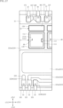
- FIG. 1 is a perspective view showing a semiconductor device according to a first embodiment of the present disclosure.
- FIG. 2 is a plan view of the semiconductor device shown in FIG. 1, and is a view through a resin member.
- FIG. 3 is a partially enlarged view of FIG. 2.
- FIG. 4 is a cross-sectional view taken along line IV-IV in FIG. 2.
- FIG. 5 is a sectional view taken along line VV in FIG. 2.
- FIG. 6 is a cross-sectional view taken along line VI-VI in FIG.
- FIG. 7 is a cross-sectional view taken along line VII-VII in FIG. 6.
- FIG. 8 is a perspective view showing a state in which a driving device is attached to the semiconductor device shown in FIG. FIG.
- FIG. 9 is a circuit diagram showing an example of the circuit configuration of the semiconductor device shown in FIG. 1.
- FIG. 10 is a flowchart showing an example of a method for manufacturing the semiconductor device shown in FIG.
- FIG. 11 is a cross-sectional view showing steps in an example of the method for manufacturing the semiconductor device shown in FIG.
- FIG. 12 is a cross-sectional view showing steps in an example of the method for manufacturing the semiconductor device shown in FIG.
- FIG. 13 is a cross-sectional view showing steps in an example of the method for manufacturing the semiconductor device shown in FIG.
- FIG. 14 is a cross-sectional view showing steps in an example of the method for manufacturing the semiconductor device shown in FIG.
- FIG. 15 is a front view showing the entire wedge tool.
- FIG. 16 is a cross-sectional view of the wedge tool shown in FIG.
- FIG. 17 is a partially enlarged plan view showing steps in an example of the method for manufacturing the semiconductor device shown in FIG.
- FIG. 18 is a cross-sectional view showing steps in an example of the method for manufacturing the semiconductor device shown in FIG.
- FIG. 19 is a cross-sectional view showing steps in an example of the method for manufacturing the semiconductor device shown in FIG.
- FIG. 20 is a cross-sectional view showing steps in an example of the method for manufacturing the semiconductor device shown in FIG.
- FIG. 21 is a front view showing steps in an example of the method for manufacturing the semiconductor device shown in FIG. 1.
- FIG. 22 is a partially enlarged sectional view showing a semiconductor device according to a first modification of the first embodiment.
- FIG. 22 is a partially enlarged sectional view showing a semiconductor device according to a first modification of the first embodiment.
- FIG. 23 is a partially enlarged plan view showing a semiconductor device according to a second modification of the first embodiment.
- FIG. 24 is a partially enlarged plan view showing a semiconductor device according to a third modification of the first embodiment.
- FIG. 25 is a partially enlarged plan view showing a semiconductor device according to a fourth modification of the first embodiment.
- FIG. 26 is a partially enlarged plan view showing a semiconductor device according to a second embodiment of the present disclosure.
- FIG. 27 is a cross-sectional view taken along line XXVII-XXVII in FIG. 26.
- FIG. 28 is a partially enlarged sectional view showing a semiconductor device according to a third embodiment of the present disclosure.
- FIG. 29 is a plan view showing a semiconductor device according to a fourth embodiment of the present disclosure, and is a view through a resin member.
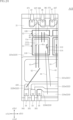
- the semiconductor device A10 includes a plurality of semiconductor elements 11, a plurality of semiconductor elements 12, a support member 2, a plurality of terminals 3, a plurality of wires 41 to 47, a buffer section 48, and a resin member 5.
- the plurality of terminals 3 include power terminals 31 and 32, signal terminals 33, detection terminals 34 and 35, and temperature detection terminals 36 and 37.
- the semiconductor device A10 is used with the drive device 7 attached.
- FIG. 1 is a perspective view showing the semiconductor device A10.
- FIG. 2 is a plan view of the semiconductor device A10.
- the outer shape of the resin member 5 is shown by an imaginary line (two-dot chain line) that is transmitted through the resin member 5.
- FIG. 3 is a partially enlarged view of FIG. 2.
- FIG. 4 is a cross-sectional view taken along line IV-IV in FIG. 2.
- FIG. 5 is a sectional view taken along line VV in FIG. 2. Note that the plurality of wires 41 to 47 are omitted in FIGS. 4 and 5.
- FIG. 6 is a cross-sectional view taken along line VI-VI in FIG.
- FIG. 7 is a cross-sectional view taken along line VII-VII in FIG. 6.
- FIG. 8 is a perspective view showing a state in which the driving device 7 is attached to the semiconductor device A10.
- FIG. 9 is a circuit diagram showing an example of the circuit configuration of the semiconductor device A10.
- the shape of the portion of the semiconductor device A10 covered with the resin member 5 when viewed in the thickness direction is rectangular.
- the thickness direction (planar view direction) of the semiconductor device A10 is defined as the z direction
- the direction in which the power terminals 31 and 32 of the semiconductor device A10 protrude perpendicularly to the z direction is defined as the x direction.
- the direction perpendicular to the z-direction and the x-direction (the vertical direction in FIG. 2) is defined as the y-direction.
- one side in the z direction (the lower side in FIGS. 4 and 5) is the z1 side
- the other side is the z2 side.
- One side in the x direction (the left side in FIG. 2) is the x1 side, and the other side (the right side in FIG. 2) is the x2 side.
- One side in the y direction (the lower side in FIG. 2) is the y1 side, and the other side (the upper side in FIG. 2) is the y2 side.
- the z direction corresponds to the "thickness direction" of the present disclosure.
- Each dimension of the semiconductor device A10 is not particularly limited.
- the plurality of semiconductor elements 11 are elements that perform the electrical functions of the semiconductor device A10.
- Each semiconductor element 11 is constructed using a semiconductor material mainly composed of SiC (silicon carbide), for example. Note that the semiconductor material is not limited to SiC, and may be Si (silicon), GaAs (gallium arsenide), GaN (gallium nitride), or the like.
- Each semiconductor element 11 is a switching element such as a MOSFET (Metal-Oxide-Semiconductor Field-Effect Transistor).
- each semiconductor element 11 is not limited to a MOSFET, and may be a field effect transistor including a MISFET (Metal-Insulator-Semiconductor FET), or a bipolar transistor such as an IGBT (Insulated Gate Bipolar Transistor).
- the plurality of semiconductor elements 11 are each an n-channel MOSFET, for example, and are all the same element. Note that each semiconductor element 11 may be a p-channel type MOSFET.
- the plurality of semiconductor elements 11 are arranged at equal intervals in the x direction and connected in parallel to each other.
- the semiconductor device A10 includes five semiconductor elements 11. Note that the number of semiconductor elements 11 is not limited to this, and can be freely set according to the performance required of the semiconductor device A10.
- Each semiconductor element 11 is bonded onto the support member 2 using a conductive bonding material 110.
- the conductive bonding material 110 is, for example, solder, silver paste, or sintered metal.
- Each semiconductor element 11 has an element main surface 11a and an element back surface 11b.
- the element main surface 1 1a and the element back surface 11b face opposite to each other in the z direction.
- the element main surface 11a faces the z2 side in the z direction.
- the back surface 11b of the element faces the z1 side in the z direction.
- the element back surface 11b faces the support member 2.
- each semiconductor element 11 has a first electrode 111, a second electrode 112, and a third electrode 113.
- the first electrode 111 and the second electrode 112 are arranged on the element main surface 11a.
- the first electrode 111 is larger than the second electrode 112 in plan view.
- the third electrode 113 is arranged on the back surface 12b of the element.
- the third electrode 113 covers substantially the entire surface of the back surface 11b of the element.
- the first electrode 111 includes a first metal layer 111a and a second metal layer 111b.
- the constituent material of the first metal layer 111a is not limited, it is Al in this embodiment.
- the second metal layer 111b is formed on the first metal layer 111a by, for example, plating.
- the second metal layer 111b may be formed by other processing.
- the constituent material of the second metal layer 111b is not limited, it is Cu in this embodiment.
- the thickness dimension (dimension in the z direction) of the second metal layer 111b is 50 ⁇ m or less.
- another conductive layer may be interposed between the first metal layer 111a and the second metal layer 111b.
- the constituent material of the second electrode 112 and the third electrode 113 is not limited, it is Al in this embodiment.
- the first electrode 111 is a source electrode
- the second electrode 112 is a gate electrode
- the third electrode 113 is a drain electrode.
- the third electrode 113 is conductively bonded to a part of the support member 2 (the conductor layer 223 of the main surface metal layer 22, which will be described later) via the conductive bonding material 110.
- the third electrode 113 is in contact with the conductive bonding material 110.
- Wires 41, 44 to 46 and a buffer section 48 are connected to the first electrode 111.
- a wire 43 is connected to the second electrode 112.
- the plurality of semiconductor elements 12 are, for example, diodes such as Schottky barrier diodes. Each semiconductor element 12 is connected in antiparallel to each semiconductor element 11, as shown in FIG.
- Each semiconductor element 12 is bonded onto the support member 2 with a conductive bonding material 120.
- the conductive bonding material 120 is, for example, solder, silver paste, or sintered metal.
- the number of semiconductor elements 12 corresponds to the number of semiconductor elements 11. Note that the semiconductor device A10 does not need to include each semiconductor element 12.
- Each semiconductor element 12 has an element main surface 12a and an element back surface 12b.
- the element main surface 12a and the element back surface 12b face opposite to each other in the z direction.
- the element main surface 12a faces the z2 side in the z direction.
- the element back surface 12b faces the z1 side in the z direction.
- the element back surface 12b faces the support member 2.
- Each semiconductor element 12 has an anode electrode 121 and a cathode electrode 122.
- the anode electrode 121 is arranged on the element main surface 12a.
- the cathode electrode 122 is arranged on the back surface 12b of the element.
- the cathode electrode 122 is electrically connected to a part of the support member 2 (the conductor layer 223 of the main surface metal layer 22, which will be described later), via the conductive bonding material 120.
- Cathode electrode 122 is in contact with conductive bonding material 120 .
- the support member 2 is a member that supports the plurality of semiconductor elements 11 and 12, respectively, and forms a conduction path between each semiconductor element 11 and the plurality of terminals 3.
- the support member 2 includes an insulating substrate 21 , a main surface metal layer 22 , and a back surface metal layer 23 .
- the insulating substrate 21 has, for example, a flat plate shape and has electrical insulation properties.
- the constituent material of the insulating substrate 21 is, for example, ceramics with excellent thermal conductivity, and in this embodiment, it is Al 2 O 3 (aluminum oxide).
- the constituent material of the insulating substrate 21 is not limited, and may be other ceramics such as AlN (aluminum nitride) and SiN (silicon nitride).
- the constituent material of the insulating substrate 21 is not limited to ceramics, and may be Si or synthetic resin.
- the constituent material of the insulating substrate 21 may be any material as long as it has insulating properties and can withstand the heat generated by the semiconductor element 11.
- the insulating substrate 21 has a main surface 211 and a back surface 212.
- the main surface 211 and the back surface 212 face opposite to each other in the z direction.
- the main surface 211 faces the z2 side in the z direction.
- the back surface 212 faces the z1 side in the z direction.
- the main surface metal layer 22 is formed on the main surface 211 of the insulating substrate 21.
- the constituent material of the main surface metal layer 22 is, for example, a metal containing Cu. Note that the constituent material of the main surface metal layer 22 is not limited.
- the main surface metal layer 22 is formed, for example, by plating. Note that the method for forming the main surface metal layer 22 is not limited.
- the main surface metal layer 22 is covered with a resin member 5.
- the main surface metal layer 22 includes conductor layers 221 to 225 and a plurality of conductor layers 226 and 227, respectively. The conductive layers 221 to 227 are spaced apart from each other.
- the conductor layer 221 includes a strip portion 221a and a terminal joint portion 221b.
- the strip portion 221a extends along the x direction, and a plurality of wires 41 and wires 42 are respectively bonded to the strip portion 221a.
- the terminal joint portion 221b is connected to the end portion of the strip portion 221a on the x2 side in the x direction, and a portion of the power terminal 32 (pad portion 321, which will be described later) is joined to the terminal joint portion 221b.
- the conductor layer 222 includes a strip portion 222a and a terminal joint portion 222b.
- the strip portion 222a extends along the x direction, and a plurality of wires 43 are respectively bonded to the strip portion 222a.
- the terminal joint portion 222b is connected to the end of the strip portion 222a on the x1 side in the x direction, and a portion of the signal terminal 33 (pad portion 331 to be described later) is joined to the terminal joint portion 222b.
- the conductor layer 223 includes a strip portion 223a and a terminal joint portion 223b.
- the strip portion 223a extends along the x direction, and a plurality of semiconductor elements 11 and 12 are bonded to each strip portion 223a. Heat from each semiconductor element 11 is appropriately transmitted to the strip portion 223a (conductor layer 223) via the conductive bonding material 110.
- the plurality of semiconductor elements 11 bonded to the strip portion 223a are arranged in the direction in which the strip portion 223a extends (x direction).
- the terminal joint portion 223b is connected to the end portion of the strip portion 223a on the x1 side in the x direction, and a portion of the power terminal 31 (pad portion 311 to be described later) is joined to the terminal joint portion 223b.
- the conductor layer 223 is electrically connected to the third electrode 113 (drain electrode) of each semiconductor element 11 via each conductive bonding material 110, and is electrically connected to each conductive bonding material 120. It is electrically connected to the cathode electrode 122 of each semiconductor element 12 via. That is, the third electrode 113 of each semiconductor element 11 and the cathode electrode 122 of each semiconductor element 12 are electrically connected via the conductor layer 223.
- the conductor layer 224 includes a strip portion 224a and a terminal joint portion 224b.
- the strip portion 224a extends along the x direction, and a plurality of wires 44 are respectively bonded to the strip portion 224a.
- the terminal joint portion 224b is connected to the end of the strip portion 224a on the x1 side in the x direction, and a portion of the detection terminal 35 (pad portion 351, which will be described later) is joined to the terminal joint portion 224b.
- the wire 42 is bonded to the conductive layer 225. Further, a portion of the detection terminal 34 (pad portion 341 described later) is bonded to the conductor layer 225.
- the plurality of strips 221a, 222a, 223a, and 224a are lined up in the y direction and overlap each other when viewed in the y direction.
- the arrangement of the plurality of strips 221a, 222a, 223a, and 224a in the y direction is not particularly limited.
- the strip portion 224a, the strip portion 222a, the strip portion 221a, and the strip portion 223a are arranged in this order from the y-direction y1 side to the y-direction y2 side.
- the strip portion 221a is arranged between the strip portion 222a and the strip portion 223a in the y direction, and the strip portion 222a is arranged between the strip portion 221a and the strip portion 224a in the y direction.
- the strip portion 223a is arranged on the opposite side of the strip portion 222a with the strip portion 221a interposed therebetween in the y direction.
- the conductor layer 225 is arranged on the x1 side of the terminal joint portion 222b of the conductor layer 222 in the x direction.
- Each of the plurality of conductor layers 226 and 227 is arranged on the y-direction y2 side of the strip portion 223a of the conductor layer 223.
- the main surface metal layer 22 includes the same number of conductor layers 226 and conductor layers 227 as the semiconductor element 11 (five in this embodiment).
- the conductor layers 226 and 227 are alternately arranged along the x direction.
- a wire 46 is bonded to each conductor layer 226 . Further, each conductor layer 226 is connected to a portion of the temperature detection terminal 36 (pad portion 361 described later).
- a wire 47 is connected to each conductor layer 227 . Further, each conductor layer 227 is connected to a portion of the temperature detection terminal 37 (pad portion 371 described later).
- each of the conductor layers 221 to 227 are not limited to those described above, and are appropriately designed depending on the arrangement position of each terminal 3 and the like.
- the back metal layer 23 is formed on the back surface 212 of the insulating substrate 21.
- the constituent material of the back metal layer 23 is, for example, a metal containing Cu. Note that the constituent material is not limited.
- the back metal layer 23 is formed, for example, by electroless plating. Note that the method for forming the back metal layer 23 is not limited. As shown in FIGS. 4 and 5, the surface of the back metal layer 23 facing the z1 side in the z direction is exposed from the resin member 5. Note that the surface facing the z-direction z1 side may be covered with the resin member 5. Further, the support member 2 does not need to include the back metal layer 23. In this case, the back surface 212 of the insulating substrate 21 may be covered with the resin member 5 or may be exposed from the resin member 5.
- Each terminal 3 is joined to the main surface metal layer 22 inside the resin member 5. Each terminal 3 protrudes from the insulating substrate 21 when viewed in the z direction. Further, each terminal 3 is partially exposed from the resin member 5. Each terminal 3 is composed of, for example, the same lead frame. Each terminal 3 is made of metal, preferably Cu or Ni, or an alloy thereof, a 42 alloy, or the like.
- the power terminal 31 is a drain terminal in the semiconductor device A10.
- the power terminal 31 is a plate-shaped member.
- the power terminal 31 is electrically connected to the third electrode 113 (drain electrode) of each semiconductor element 11 via the conductor layer 223 and the conductive bonding material 110.
- the power terminal 31 includes a pad portion 311 and a terminal portion 312.
- the pad portion 311 is covered with the resin member 5.
- the pad portion 311 is bonded to the conductor layer 223. This joining may be performed by any method such as joining using a conductive joining material (solder, silver paste, sintered metal, etc.), laser joining, or ultrasonic joining.
- the terminal portion 312 is exposed from the resin member 5. As shown in FIG. 2, the terminal portion 312 extends from the resin member 5 toward the x1 side in the x direction when viewed in the z direction. Note that the surface of the terminal portion 312 may be plated with silver, for example.
- the power terminal 32 is a source terminal in the semiconductor device A10.
- the power terminal 32 is a plate-shaped member.
- the power terminal 32 is electrically connected to the first electrode 111 (source electrode) of each semiconductor element 11 via the conductor layer 221 and the plurality of wires 41.
- the power terminal 32 includes a pad portion 321 and a terminal portion 322.
- the pad portion 321 is covered with the resin member 5.
- the pad portion 321 is bonded to the conductive layer 221. This bonding may be performed by any method such as bonding using a conductive bonding material, laser bonding, or ultrasonic bonding.
- the terminal portion 322 is exposed from the resin member 5. As shown in FIG. 2, the terminal portion 322 extends from the resin member 5 toward the x2 side in the x direction when viewed in the z direction. Note that the surface of the terminal portion 322 may be plated with silver, for example.
- the signal terminal 33 is a gate terminal in the semiconductor device A10.
- the signal terminal 33 is electrically connected to the second electrode 112 (gate electrode) of each semiconductor element 11 via the conductor layer 222 and the plurality of wires 43.
- a drive signal for controlling on/off of each semiconductor element 11 is input to the signal terminal 33 .
- a drive circuit DR is connected to the signal terminal 33, as shown in FIG.
- the drive circuit DR generates a drive signal that controls the switching operation of each semiconductor element 11.
- a drive signal is input to the signal terminal 33 from the drive circuit DR.
- the drive circuit DR shown in FIG. 9 is an example, and the drive circuit DR is not limited to the illustrated circuit configuration.
- the signal terminal 33 includes a pad portion 331 and a terminal portion 332.
- the pad portion 331 is covered with the resin member 5.
- Pad portion 331 is bonded to conductor layer 222 . This bonding may be performed by any method such as bonding using a conductive bonding material, laser bonding, or ultrasonic bonding.
- the terminal portion 332 is exposed from the resin member 5.
- the terminal portion 332 is L-shaped when viewed in the x direction.
- the detection terminal 34 is a source sense terminal in the semiconductor device A10.
- the detection terminal 34 is electrically connected to the first electrode 111 (source electrode) of the semiconductor element 11 via the conductor layer 225, the wire 42, the conductor layer 221, and the plurality of wires 41.
- a drive circuit DR is connected to the detection terminal 34, as shown in FIG.
- the voltage applied to the detection terminal 34 is input to the drive circuit DR as a feedback signal.
- the detection terminal 34 includes a pad portion 341 and a terminal portion 342.
- the pad portion 341 is covered with the resin member 5.
- the pad portion 341 is bonded to the conductor layer 225. This bonding may be performed by any method such as bonding using a conductive bonding material, laser bonding, or ultrasonic bonding.
- the terminal portion 342 is exposed from the resin member 5.
- the terminal portion 342 is L-shaped when viewed in the x direction.
- the detection terminal 35 is a source sense terminal in the semiconductor device A10.
- the detection terminal 35 is electrically connected to the first electrode 111 (source electrode) of each semiconductor element 11 via the conductor layer 224 and the plurality of wires 44 .
- a mirror clamp circuit MC external to the semiconductor device A10 is connected between the detection terminal 35 and the signal terminal 33.
- the Miller clamp circuit MC is a circuit for preventing malfunction (erroneous gate ON) of each semiconductor element 11, and includes, for example, a MOSFET, as shown in FIG.
- the source terminal of the MOSFET is connected to the detection terminal 35, and the drain terminal of the MOSFET is connected to the signal terminal 33.
- the gate-source voltage of the semiconductor element 11 is forced to approximately 0 (zero) V or a negative bias voltage, and the gate of the semiconductor element 11 is turned on. Eliminate potential rise.
- the detection terminal 35 includes a pad portion 351 and a terminal portion 352.
- the pad portion 351 is covered with the resin member 5.
- the pad portion 351 is bonded to the conductor layer 224. This bonding may be performed by any method such as bonding using a conductive bonding material, laser bonding, or ultrasonic bonding.
- the terminal portion 352 is exposed from the resin member 5. As shown in FIG. 4, the terminal portion 352 is L-shaped when viewed in the x direction.
- the detection terminal 34, the signal terminal 33, and the detection terminal 35 are arranged in this order along the x direction from the x1 side to the x2 side as shown in FIGS. 2 and 3, and as shown in FIG. They overlap in the x direction.
- the detection terminal 34, the signal terminal 33, and the detection terminal 35 protrude from the resin side surface 533 on the y1 side in the y direction.
- the plurality of temperature detection terminals 36 and 37 are terminals for detecting the temperature of the semiconductor element 11, respectively.
- One temperature detection terminal 36 and one temperature detection terminal 37 are provided for each semiconductor element 11 .
- the semiconductor device A10 since the semiconductor device A10 includes five semiconductor elements 11, it includes five temperature detection terminals 36 and five temperature detection terminals 37.
- Each temperature detection terminal 36 is connected to the conductor layer 226, respectively.
- Each temperature detection terminal 36 is electrically connected to the wire 46 via the conductor layer 226.
- Each temperature detection terminal 37 is connected to the conductor layer 227, respectively.
- Each temperature detection terminal 37 is electrically connected to the wire 47 via the conductor layer 227.
- the temperature detection terminal 36 includes a pad portion 361 and a terminal portion 362.
- the pad portion 361 is covered with the resin member 5.
- Pad portion 361 is bonded to conductor layer 226. This bonding may be performed by any method such as bonding using a conductive bonding material, laser bonding, or ultrasonic bonding.
- the terminal portion 362 is exposed from the resin member 5. As shown in FIG. 4, the terminal portion 362 is L-shaped when viewed in the x direction.
- the temperature detection terminal 37 includes a pad portion 371 and a terminal portion 372.
- the pad portion 371 is covered with the resin member 5.
- the pad portion 371 is bonded to the conductor layer 227. This bonding may be performed by any method such as bonding using a conductive bonding material, laser bonding, or ultrasonic bonding.
- the terminal portion 372 is exposed from the resin member 5.
- the terminal portion 372 is L-shaped when viewed in the x direction.
- the plurality of temperature detection terminals 36 and the plurality of temperature detection terminals 37 are arranged alternately along the x direction as shown in FIGS. 2 and 3, and overlap in the x direction as shown in FIG. .
- Each temperature detection terminal 36, 37 protrudes from the resin side surface 534 on the y2 side in the y direction.
- Each of the plurality of wires 41 to 45 provides electrical continuity between two separated parts.
- Each of the wires 41 to 45 is a so-called bonding wire.
- each wire 41-45 is formed by wedge bonding.
- each wire 41 to 45 may be formed by ball bonding.
- the constituent material of each wire 41 to 45 is, for example, Al, Au, Cu, or an alloy containing any of these, and is not limited. In this embodiment, a case will be described in which the constituent material of each wire 41 to 45 is Cu.
- the diameter of each wire 41, 42, 45 through which a relatively large current flows is larger than the diameter of each wire 43, 44 through which only a relatively small current flows.
- the diameter of each wire 41, 42, 45 is, for example, about 400 ⁇ m, and the diameter of each wire 43, 44 is, for example, about 150 ⁇ m. Note that the diameter of each wire 41 to 45 is not limited.
- Each of the plurality of wires 41 has one end connected to the first electrode 111 (source electrode) and the other end connected to the conductor layer 221.
- Each wire 41 connects the first electrode 111 of each semiconductor element 11 and the conductor layer 221.
- the wire 42 has one end joined to the conductor layer 221 and the other end joined to the conductor layer 225.
- the wire 42 connects the conductor layer 221 and the conductor layer 225 to each other. Note that the other end of the wire 42 may be bonded to the pad portion 341 of the detection terminal 34 instead of being bonded to the conductor layer 225.
- each of the plurality of wires 43 is connected to the second electrode 112 (gate electrode) of each semiconductor element 11, and the other end is connected to the conductor layer 222.
- Each wire 43 connects each second electrode 112 and the conductor layer 222.
- Each of the plurality of wires 44 has one end connected to the first electrode 111 (source electrode) and the other end connected to the conductor layer 224.
- Each wire 44 connects the first electrode 111 of each semiconductor element 11 and the conductor layer 224.
- Each wire 44 is a sense line connected to the first electrode 111 (source electrode) of each semiconductor element 11 in Kelvin.
- each of the plurality of wires 45 is connected to the first electrode 111 (source electrode), and the other end is connected to the anode electrode 121 of each semiconductor element 12.
- Each wire 45 connects the first electrode 111 of each semiconductor element 11 and the anode electrode 121 of each semiconductor element 12 to each other.
- the plurality of wires 46 and 47 are members for detecting the temperature of the semiconductor element 11, respectively.
- Each wire 46, 47 is formed by the bonding wire forming method similarly to the wires 41 to 45. In this embodiment, each wire 46, 47 is formed by wedge bonding. Note that each wire 46, 47 may be formed by ball bonding.
- Each wire 46 has one end joined to the first electrode 111 (second metal layer 111b) and the other end joined to the conductor layer 226.
- Each wire 46 connects the first electrode 111 of each semiconductor element 11 and each conductor layer 226 to each other.
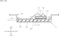
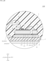
- Each wire 47 has one end connected to the buffer section 48 disposed on the first electrode 111 (second metal layer 111b), and the other end connected to the conductor layer 227.
- Each wire 47 connects the buffer section 48 and each conductor layer 227 to each other. Further, in this embodiment, since only a relatively small current flows through each wire 46, 47, the diameter of each wire 46, 47 is approximately the same as that of each wire 43, 44 (for example, about 150 ⁇ m). Note that the diameter of each wire 46, 47 is not limited.
- the constituent material of the wire 46 is the second metal.
- the second metal is Cu, which is the same as the second metal layer 111b of the first electrode 111.
- the constituent material of the wire 47 is a first metal whose thermoelectric power is different from that of the second metal. Thermoelectric power is the thermoelectromotive force per 1K when a temperature difference is created between both ends of a conductive substance.
- the first metal is constantan (an alloy of Cu and Ni: 55Cu-45Ni).
- the wire 46 (Cu), the second metal layer 111b (Cu) of the first electrode 111, the buffer portion 48 (which is Cu as described later), and the wire 47 (constantan) function as a thermocouple.
- thermocouples based on Cu and constantan are widely known as T-type thermocouples.
- a contact point 47a between the wire 47 and the buffer portion 48 corresponds to a temperature measuring contact point (thermal contact point) of a thermocouple.
- the contact between the wire 46 and the conductor layer 226 and the contact between the wire 47 and the conductor layer 227 correspond to a reference junction (cold junction) of the thermocouple.
- a voltage is generated between the reference junctions depending on the temperature difference between the reference junction and the temperature measurement junction.
- the temperature detection terminals 36 and 37 output the voltage between the reference junctions to the drive device 7 as a signal for detecting the temperature of the semiconductor element 11.
- the buffer section 48 is bonded to the first electrode 111 (second metal layer 111b), and is a member for absorbing impact on the semiconductor element 11 when the wire 47 is bonded.
- the wire 47 is made of a first metal (constantan). Therefore, the wire 47 has a larger Vickers hardness than the second metal layer 111b whose constituent material is Cu. Furthermore, since the second metal layer 111b is formed by plating, its thickness is relatively small (50 ⁇ m or less). Therefore, if the wire 47 is bonded to the first electrode 111 by wedge bonding, the semiconductor element 11 may be damaged by the impact.
- the buffer part 48 is electrically connected to the second metal layer 111b of the first electrode 111, and the wire 47 is electrically connected to the buffer part 48, thereby absorbing the impact on the semiconductor element 11. control damage.
- the constituent material of the buffer section 48 is Cu, which is the same as the second metal layer 111b of the first electrode 111 and the wire 46.
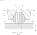
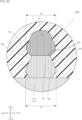
- the buffer section 48 is a piece of wire made by joining wire materials together by wedge bonding. As will be described later, unlike normal wire bonding, the buffer portion 48 is formed by first bonding, stretching the wire material a little, and immediately cutting it. In this embodiment, the buffer section 48 is formed using the same wire material as each wire 41, 42, 45. Therefore, the constituent material of the buffer section 48 is Cu, similarly to the wires 41, 42, and 45. Further, the dimension in the direction perpendicular to the extending direction of the buffer section 48 (hereinafter sometimes referred to as "diameter") is approximately the same as the diameter of each wire 41, 42, 45 (for example, approximately 400 ⁇ m), and each It is larger than the diameter of wire 47. Note that the buffer portion 48 may be formed using a wire material different from that of the wires 41, 42, and 45, and the diameter of the buffer portion 48 is not limited.
- the shape of the buffer portion 48 is such that a substantially cylindrical wire material is pressed against the first electrode 111 by wedge bonding and crushed.
- the buffer portion 48 includes a top surface 481, a bottom surface 482, a pair of pressed surfaces 483, and a cut surface 484.
- the top surface 481 and the bottom surface 482 face oppositely to each other in the z direction.
- the top surface 481 faces the z2 side in the z direction, and the bottom surface 482 faces the z1 side in the z direction.
- the bottom surface 482 is a flat surface in contact with the first electrode 111.
- a wire 47 is bonded to the top surface 481.
- the pair of pressed surfaces 483 are arranged on both sides of the top surface 481 when viewed in the z direction (in the example of FIG. 7, on both sides in the x direction). As will be described later, the pair of pressed surfaces 483 are surfaces formed by pressing the guide groove of the wedge, and the shape of the guide groove of the wedge appears. The pair of pressed surfaces 483 are each flat, and are further away from each other toward the z1 side in the z direction.
- the cut surface 484 is a surface cut by wedge bonding, and faces the direction in which the buffer portion 48 extends (in the example of FIG. 6, the y-direction y1 side). As shown in FIG. 6, the cut surface 484 is inclined with respect to a plane perpendicular to the direction in which the buffer portion 48 extends. Note that the shape of the buffer section 48 is not limited.
- the direction in which the buffer portion 48 extends (the y direction in the example of FIG. 6) is the same as the direction in which the wire 47 extends.
- the dimension D1 in the direction in which the pair of pressed surfaces 483 of the buffer section 48 are lined up (the x direction in the example of FIG. 7) is derived from the diameter of the wire material, and is therefore approximately the same as the diameter of the wire material.
- the dimension D2 of the wire 47 in the same direction is derived from the diameter of the wire material of the wire 47, and is therefore approximately the same as the diameter of the wire 47.
- Dimension D1 is larger than dimension D2 and larger than the diameter of wire 47.
- the dimension D1 is twice or more the dimension D2.
- the wire 47 is included in the top surface 481 in the direction in which the pair of pressed surfaces 483 are lined up (the x direction in the example of FIG. 7). Note that the wire 47 may protrude from the top surface 481.
- the resin member 5 is an electrically insulating semiconductor sealing material.
- the resin member 5 includes the entire plurality of semiconductor elements 11, the plurality of semiconductor elements 12, the insulating substrate 21, the main surface metal layer 22, the plurality of wires 41 to 47, and the plurality of buffer sections 48, and a part of each of the terminals 3. and covers.
- the constituent material of the resin member 5 is, for example, epoxy resin. Note that the constituent material of the resin member 5 is not limited.
- the resin member 5 is formed, for example, by transfer molding using a mold. Note that the method for forming the resin member 5 is not limited. As shown in FIGS. 2, 4, and 5, the resin member 5 has a resin main surface 51, a resin back surface 52, and a plurality of resin side surfaces 531 to 534.
- the resin main surface 51 and the resin back surface 52 face opposite to each other in the z direction.
- the main resin surface 51 faces the z2 side in the z direction
- the resin back surface 52 faces the z1 side in the z direction.
- the back metal layer 23 is exposed from the resin back surface 52, and the resin back surface 52 and the surface of the back metal layer 23 facing in the z direction z1 are flush with each other.
- Each of the plurality of resin side surfaces 531 to 534 is connected to both the resin main surface 51 and the resin rear surface 52, and is sandwiched between them. As shown in FIG. 2, the two resin side surfaces 531 and 532 face oppositely to each other in the x direction.
- the resin side surface 531 is a surface disposed on the x1 side in the x direction and facing the x1 side in the x direction.
- the resin side surface 532 is a surface disposed on the x2 side in the x direction and facing the x2 side in the x direction.
- the two resin side surfaces 533 and 534 face opposite to each other in the y direction.
- the resin side surface 533 is a surface disposed on the y1 side in the y direction and facing the y1 side in the y direction.
- the resin side surface 534 is a surface disposed on the y2 side in the y direction and facing the y2 side in the y direction.
- the resin side surfaces 531 to 534 each have a surface that is connected to the resin main surface 51 and slopes closer to each other toward the resin main surface 51. That is, the portion of the resin member 5 surrounded by the inclined surfaces connected to the main resin surface 51 has a tapered shape in which the cross-sectional area in the xy plane becomes smaller toward the main resin surface 51. Furthermore, the resin side surfaces 531 to 534 each have a surface that is connected to the resin back surface 52 and slopes closer to each other toward the resin back surface 52. That is, the portion of the resin member 5 surrounded by the inclined surfaces connected to the main resin surface 51 has a tapered shape in which the cross-sectional area in the xy plane becomes smaller toward the resin back surface 52. Note that the shape of the resin member 5 shown in FIGS. 1 to 5 is an example. The shape of the resin member 5 is not limited to the illustrated shape.
- the driving device 7 is a device that drives the semiconductor device A10, and as shown in FIG. 8, is attached to the z-direction z2 side of the semiconductor device A10.
- the drive device 7 includes a substrate 71, terminals 723, 724, 725, and a plurality of terminals 721, 722, respectively.
- the substrate 71 is, for example, flat and has electrical insulation properties.
- the constituent material of the substrate 71 is not limited.
- Substrate 71 has a main surface 711 and a back surface 712.
- the main surface 211 and the back surface 712 face opposite to each other in the z direction.
- the main surface 711 faces the z2 side in the z direction.
- the back surface 712 faces the z1 side in the z direction.
- Wiring is formed on the main surface 711, and external connectors and a large number of electronic components are mounted, but in FIG. 8, the wiring, external connectors, electronic components, etc. on the main surface 711 are omitted. There is.
- Each of the terminals 721 to 725 is a cylindrical metal member, and is inserted into a through hole that penetrates in the z direction from the main surface 711 to the back surface 712 of the substrate 71.
- Each of the terminals 721 to 725 is electrically connected to a wiring formed on the main surface 711, respectively.
- the terminal portions 332, 342, 352, 362, and 372 of the terminals 33 to 37 of the semiconductor device A10 are inserted into each of the terminals 721 to 725, respectively, and are joined by, for example, solder.
- the signal terminal 33 is connected to the terminal 723.
- the detection terminal 34 is connected to the terminal 724.
- the detection terminal 35 is connected to the terminal 725.
- Five terminals 721 are arranged like the temperature detection terminals 36, and each terminal 721 is connected to the temperature detection terminal 36, respectively. Since the temperature detection terminal 36 is electrically connected to the wire 46 via the conductor layer 226, the terminal 721 is electrically connected to the wire 46.
- Five terminals 722 are arranged like the temperature detection terminals 37, and each terminal 722 is connected to the temperature detection terminal 37, respectively. Since the temperature detection terminal 37 is electrically connected to the wire 47 via the conductor layer 227, the terminal 722 is electrically connected to the wire 47.
- the drive device 7 includes a plurality of relative temperature detection sections 73, a plurality of reference junction compensation sections 74, an overheat protection section 75, and a drive control section 76 as functional configurations.
- the drive control unit 76 is a functional configuration that controls the switching operation of each semiconductor element 11, and is realized by, for example, a gate drive IC.
- the drive control section 76 includes a drive circuit DR, a Miller clamp circuit MC, and the like.
- the drive control unit 76 generates a drive signal based on a control signal input from the outside, and outputs the drive signal to the semiconductor device A10 via the terminal 723.
- the semiconductor device A10 receives a drive signal from the signal terminal 33 connected to the terminal 723, and controls the switching operation of each semiconductor element 11. Further, the drive control unit 76 receives a signal from the detection terminal 34 of the semiconductor device A10 via the terminal 724, and receives a signal from the detection terminal 35 via the terminal 725. Note that the specific circuit configuration and aspect of the drive control section 76 are not limited.
- the relative temperature detection section 73 and the reference junction compensation section 74 are functional configurations for detecting the temperature of the semiconductor element 11.
- Five relative temperature detectors 73 and five reference junction compensators 74 are provided, each corresponding to the number of semiconductor elements 11 of semiconductor device A10.
- Each relative temperature detection section 73 receives voltage from a pair of temperature detection terminals 36 and 37 of the semiconductor device A10 via a pair of terminals 721 and 722.
- the voltage is the voltage between the reference junction of the thermocouple that includes the wire 46, the second metal layer 111b of the first electrode 111, the buffer section 48, and the wire 47, and is caused by the temperature difference between the reference junction and the temperature measurement junction.
- the voltage is appropriate. That is, the voltage corresponds to the relative temperature of the semiconductor element 11 with respect to the temperature of the reference junction.
- Each relative temperature detection section 73 detects the relative temperature of the corresponding semiconductor element 11 based on the input voltage.
- Each reference junction compensation section 74 converts the relative temperature detected by the corresponding relative temperature detection section 73 into an absolute temperature.
- Each reference junction compensation section 74 includes a temperature detection section having, for example, a diode, disposed adjacent to the corresponding terminal 721, 722. Note that the temperature detection section may include a temperature sensor such as a thermistor.
- the temperature detection terminals 36 and 37 connected to the terminals 721 and 722 are connected to the conductor layers 226 and 227.
- the temperature detection section indirectly detects the temperature of the reference junction of the thermocouple by detecting the temperature of the terminals 721 and 722.
- the reference junction compensation unit 74 converts the relative temperature detected by the corresponding relative temperature detection unit 73 into an absolute temperature by adding the temperature of the reference junction detected by the temperature detection unit.
- the reference junction compensation section 74 outputs the absolute temperature of the corresponding semiconductor element 11 to the overheat protection section 75 .
- the specific circuit configurations of the relative temperature detection section 73 and the reference junction compensation section 74 are not limited.
- the following configuration may be used. That is, the relative temperature detection section 73 transmits the voltage between the pair of terminals 721 and 722 to the reference junction compensation section 74 as a voltage according to the relative temperature of the corresponding semiconductor element 11.
- the reference junction compensation unit 74 converts the voltage corresponding to the temperature of the reference junction detected by the temperature detection unit into a voltage corresponding to the thermoelectromotive force of the thermocouple, and adds it to the voltage transmitted from the relative temperature detection unit 73. and outputs it to the overheat protection section 75.
- a voltage corresponding to the absolute temperature of the semiconductor element 11 is input to the overheat protection section 75 .
- the overheat protection unit 75 detects an overheat abnormality in the corresponding semiconductor element 11 based on the absolute temperature input from each reference junction compensation unit 74.
- the overheat protection section 75 outputs an abnormality detection signal to the drive control section 76 when the absolute temperature input from each reference junction compensation section 74 becomes equal to or higher than the threshold temperature.
- the drive control unit 76 receives the abnormality detection signal, it stops driving the semiconductor device A10 by stopping the output of the drive signal.
- the specific circuit configuration of the overheat protection section 75 is not limited.
- the overheat protection section 75 may include a comparator that generates an abnormality detection signal when the voltage according to the absolute temperature input from the reference junction compensation section 74 becomes equal to or higher than the voltage according to the threshold temperature. .
- FIG. 10 is a flowchart illustrating an example of a method for manufacturing the semiconductor device A10.
- 11 to 14 and 17 to 21 are diagrams showing steps in an example of the method for manufacturing the semiconductor device A10.
- 11 to 14 and FIGS. 19 to 20 are cross-sectional views corresponding to FIG. 4.
- FIG. 17 is a partially enlarged plan view corresponding to FIG. 3.
- FIG. 18 is a cross-sectional view and corresponds to FIG. 7.
- FIG. 21 is a front view. 15 and 16 are diagrams for explaining wedge bonding. Note that the x direction, y direction, and z direction shown in FIGS. 11 to 21 indicate the same directions as in FIGS. 1 to 8.
- the manufacturing method of the semiconductor device A10 includes a support member forming step (S1), a lead frame bonding step (S2), a semiconductor element mounting step (S3), a wire forming step (S4), and a resin forming step ( S5), and a frame cutting step (S6).
- the support member forming step (S1) is a step of forming the support member 2.
- the insulating substrate 91 is prepared (S11).
- the insulating substrate 91 is made of ceramic, for example, and has a main surface 911 and a back surface 912 facing oppositely to each other in the z direction.
- a main surface metal layer 22 is formed on the main surface 911 of the insulating substrate 91 (S12).
- the main surface metal layer 22 is formed by forming a base layer covering the entire main surface 911 by, for example, electroless plating or sputtering, forming a mask, forming a plating layer by electrolytic plating, and etching to eliminate the need for the base layer.
- a back metal layer 23 is formed on the back surface 912 of the insulating substrate 91 (S13).
- the back metal layer 23 is formed, for example, by electroless plating. Note that by using a DBC (Direct Bonding Copper) substrate in which Cu foil is bonded to the main surface 911 and the back surface 912 of the insulating substrate 91, the main surface metal is bonded to the insulating substrate 91 by patterning the Cu foil on the main surface 911 side. Layer 22 and back metal layer 23 may be formed.
- the insulating substrate 91 is cut (S14).
- the insulating substrate 21 is formed by cutting the insulating substrate 91. Through the above steps, the support member 2 is formed.
- the lead frame 92 that will become each terminal 3 is prepared.
- the lead frame 92 includes a portion that becomes each terminal 3, and further has a frame to which a plurality of terminals 3 are connected. Note that the shape etc. of the lead frame 92 are not limited at all.
- a conductive bonding paste is placed at the position of the main surface metal layer 22 where each terminal 3 is to be bonded, and as shown in FIG. do. For example, a portion of the lead frame 92 that will become the detection terminal 35 is bonded to the conductive layer 224. Further, a portion of the lead frame 92 that will become the detection terminal 36 is joined to the conductive layer 226. Note that the method of joining the lead frame 92 is not limited.
- a conductive bonding paste 93 is placed in the region of the conductor layer 223 where the semiconductor elements 11 and 12 are to be placed.
- the conductive bonding paste 93 is, for example, solder, silver paste, or sintered metal.
- the plurality of semiconductor elements 11 and the plurality of semiconductor elements 12 are attached to the conductive bonding paste 93, heated, and then cooled.
- the conductive bonding paste 93 interposed between the conductive layer 223 and the semiconductor element 11 becomes the conductive bonding material 110, and the semiconductor element 11 is bonded to the conductive layer 223 via the conductive bonding material 110.
- Ru Further, the conductive bonding paste 93 interposed between the conductive layer 223 and the semiconductor element 12 becomes the conductive bonding material 120, and the semiconductor element 12 is bonded to the conductive layer 223 via the conductive bonding material 120.
- the wires 41 to 47 and the buffer portion 48 are formed by wedge bonding. Wedge bonding is performed using a wedge tool.
- 15 and 16 show an example of a wedge tool.
- FIG. 15 is a front view showing the entire wedge tool 6.
- FIG. 16 is a cross-sectional view of the wedge tool 6 shown in FIG. 15 taken along the line XVI-XVI.
- the wedge tool 6 includes a wedge 61, a wire guide 62, and a cutter 63.
- the wedge 61 presses the wire material 69 against the object to be welded 68 and joins it by ultrasonic vibration.
- the wedge 61 has a guide groove 611 formed therein.
- the guide groove 611 is provided at the lower end of the wedge 61 (on the z1 side in the z direction).
- the guide groove 611 has a V-shaped cross section and a pair of inner surfaces 611a, as shown in FIG. 16.
- Ultrasonic vibration is applied to the wedge 61 in the direction of the white arrow shown in FIG. 15 when the wire material 69 is joined.
- the wire guide 62 is fixed to the wedge 61 and guides a wire material 69 wound on a wire reel (not shown) to the wedge 61.
- Cutter 63 cuts wire material 69.
- the cutter 63 is located adjacent to the wedge 61.
- the wire guide 62 and the cutter 63 are placed on opposite sides of the wedge 61.
- the wedge 61 is pressed against the welding object 68 with the wire material 69 disposed in the guide groove 611 and is subjected to vibration. Thereby, the tip portion of the wire material 69 and the bonding target 68 are bonded by ultrasonic welding (first bonding). In the case of normal wire bonding, the wedge tool 6 then moves while pulling out the wire material 69, joins the wire material 69 to another bonding target 68 by ultrasonic welding (second bonding), and transfers the wire material 69 to the cutter 63. Cut by. As a result, bonding wires having both ends bonded to the two objects 68 to be bonded are formed. On the other hand, when forming the buffer portion 48, the wedge tool 6 moves a little in the direction of the black arrow shown in FIG. 15, and then cuts the wire material 69 with the cutter 63. As a result, the wire piece, which is the cut end of the wire material 69, is joined as the buffer portion 48.
- a buffer portion 48 is formed on the first electrode 111 of the semiconductor element 11 (S41).
- Each buffer portion 48 is formed near the center of each first electrode 111 in the y direction so as to extend in the y direction toward the x1 side in the x direction. Since the wire 47 is bonded as described later, the buffer portion 48 is arranged in accordance with the position where the wire 47 is bonded, and is formed to extend in the same direction as the wire 47 extends.
- the buffer section 48 is formed by joining the tip of a wire material 691 (for example, a Cu wire) to the first electrode 111 by ultrasonic welding, moving the wedge tool 6 a little, and then cutting the wire material 691 with the cutter 63.
- Each pressed surface 483 is a surface whose cross section is retracted toward the central axis Ox side of the wire material 691 from the outer circumferential surface 489 having an arcuate shape. Since each inner surface 611a is flat, each pressed surface 483 is flat. Furthermore, as the wire material 691 is cut by the cutter 63, a cut surface 484 is formed in the buffer portion 48, as shown in FIG. The cutting surface 484 is inclined with respect to a plane perpendicular to the direction in which the buffer section 48 extends, depending on the shape of the cutter 63.
- wires 41, 42, and 45 are formed by wedge bonding (S42).
- the same wedge tool 6 and the same wire material 691 as in the formation of the buffer section 48 are used, but unlike the formation of the buffer section 48, normal wire bonding is performed.
- the wire 41 is formed to connect the first electrode 111 of the semiconductor element 11 and the conductor layer 221.
- the wire 42 is formed to connect the conductor layer 221 and the conductor layer 225.
- the wire 45 is formed to connect the first electrode 111 and the anode electrode 121 of the semiconductor element 12 .
- the order of forming the wires 41, 42, and 45 is not limited. Further, the order of the step S41 and the step S42 may be reversed.
- wires 43, 44, and 46 are formed by wedge bonding (S43).
- a wire material 692 having the same constituent material as the wire material 691 used in S42 but having a different diameter is used.
- the diameter of wire material 692 is smaller than the diameter of wire material 691.
- the wire 43 is formed to connect the second electrode 112 of the semiconductor element 11 and the conductor layer 222.
- the wire 44 is formed to connect the first electrode 111 and the conductor layer 224.
- the wire 46 is formed to connect the first electrode 111 and the conductor layer 226. Note that the order of forming the wires 43, 44, and 46 is not limited.
- the wire 47 is formed by wedge bonding (S44).
- a wire material 693 whose constituent material is different from the wire material 692 used in S43 is used.
- the wire materials 691 and 692 whose constituent material is Cu are used in S41 to S43, but the wire material 693 whose constituent material is constantan is used in S44.
- the diameter of the wire material 693 used in S44 is approximately the same as the diameter of the wire material 692 used in S43, and smaller than the diameter of the wire material 691 used in S42.
- Wire 47 is formed using the same equipment and in the same manner as wires 43, 44, and 46, except that the wire material 693 used is different.
- the wire 47 is first joined to the top surface 481 of the buffer section 48 that is joined to the first electrode 111.
- FIG. 21 shows a state in which the wedge tool 6 is moving while pulling out the wire material 693 (wire 47) after bonding to the buffer portion 48 (first bonding).
- the wire 47 is bonded onto the top surface 481 along the direction in which the buffer section 48 extends, and is formed to extend in that direction.
- the wire 47 is made of constantan and is harder than the wire 46 made of Cu, but it is not directly joined to the first electrode 111 but is joined to the buffer section 48 . Therefore, the impact on the semiconductor element 11 during bonding is suppressed.
- the wedge tool 6 moves to bond the wire material 693 to the conductor layer 227 by ultrasonic welding (second bonding), and cut the wire material 693 with the cutter 63.
- the wire 47 is formed so as to connect the buffer section 48 joined to the first electrode 111 and the conductor layer 227 (see FIGS. 3 and 6).
- the step S44 may be performed before the step S43.
- the wire 46 is joined to the first electrode 111, and the wire 47 is joined to the buffer section 48 joined to the first electrode 111, thereby forming a thermocouple.
- a part of the lead frame 92, a part of the support member 2, the plurality of semiconductor elements 11 and 12, the plurality of wires 41 to 47, and the buffer section 48 are surrounded by a mold.
- a liquid resin material is injected into the space defined by the mold.
- the resin member 5 is obtained by curing this resin material.
- the lead frame 92 is cut at an appropriate location exposed from the resin member 5. Thereby, each terminal 3 is divided from each other. After this, the above-described semiconductor device A10 is obtained by performing a process such as bending each terminal 3 as necessary.
- the buffer section 48 is joined to the first electrode 111.
- the wire 47 is not directly connected to the first electrode 111 but is connected to the buffer section 48 . Since the buffer portion 48 absorbs the impact when the wires 47 are bonded, the semiconductor device A10 can alleviate the impact applied to the semiconductor element 11. Further, the buffer portion 48 is formed using a wire material 691 by wedge bonding.
- the buffer section 48 can be formed using the same wedge tool 6 and the same wire material 691 as those for forming the wires 41, 42, and 45 (S42), so the manufacturing process can be simplified by forming it continuously with the step S42. can be converted into Therefore, the semiconductor device A10 can suppress an increase in manufacturing cost.
- the dimension D1 in the direction in which the pair of pressed surfaces 483 of the buffer section 48 are lined up is the dimension D1 in the direction in which the pair of pressed surfaces 483 of the buffer section 48 are arranged. It is larger than dimension D2 (comparable to the diameter of wire material 693 for forming wire 47). Therefore, when joining the wire 47 to the buffer portion 48, it is possible to prevent the wire 47 from slipping off the top surface 481. Further, according to the present embodiment, the wire 47 is enclosed in the top surface 481 in the direction in which the pair of pressed surfaces 483 are lined up. Therefore, when joining the wire 47 to the buffer portion 48, it is possible to further suppress the wire 47 from slipping off the top surface 481.
- the direction in which the buffer portion 48 extends matches the direction in which the wire 47 extends. Therefore, it is easier to join the wire 47 to the buffer section 48 compared to the case where the directions do not match.
- one end of the wire 46 is bonded to the second metal layer 111b of the first electrode 111, and one end of the wire 47 is bonded to the buffer portion 48 bonded to the second metal layer 111b. are joined.
- the constituent material of the wire 46 is a second metal (Cu), which is the same metal (Cu) as the constituent material of the second metal layer 111b and the buffer section 48.
- the constituent material of the wire 47 is a first metal (constantan) having a different thermoelectric power from the second metal.
- the wire 46, the second metal layer 111b, the buffer section 48, and the wire 47 function as a thermocouple, and the temperature can be detected by using the contact 47a between the wire 47 and the buffer section 48 as a temperature measuring junction of the thermocouple.
- the contact 47a is in contact with a buffer section 48 through which heat from the semiconductor element 11 is appropriately transmitted.
- the semiconductor device A10 can detect the temperature of each semiconductor element 11 with higher accuracy than when the temperature sensor is placed near the semiconductor element 11.
- the thermocouple functions as a T-type thermocouple.
- the wires 46 and 47 are formed by the bonding wire forming method similarly to the wires 41 to 45. Therefore, wires 46 and 47 can be formed using the same equipment and using the same techniques as wires 41-45. In particular, wire 46 can be formed using the same wire material 692 as wires 43, 44 and in the same process as wires 43, 44. Therefore, the manufacturing process is not complicated due to the formation of the structure for detecting temperature.
- the drive device 7 includes a relative temperature detection section 73 and a reference junction compensation section 74. Therefore, the drive device 7 converts the relative temperature of each semiconductor element 11 detected by the thermocouple formed in the semiconductor device A10 into an absolute temperature, which can be used for overheat protection.
- the present invention is not limited to this.
- the first metal and the second metal may be metals having different electrolytic abilities.
- the second metal may be Cu and the first metal may be Al.
- Cu and Al have the same polarity but different electrolytic capacities, so the wire 46, the second metal layer 111b, the buffer section 48 (Cu), and the wire 47 (Al) can be used as a thermocouple. Function.
- Al is commonly used as a bonding wire, and compared to constantan wire, it is easily available at a low price.
- the combination of the first metal and the second metal may be Chromel (registered trademark) (90Ni-10Cr) and Alumel (registered trademark) (94Ni-3Al-1Si-2Mg) like a K-type thermocouple. , Fe and constantan as in a J-type thermocouple, or chromel and constantan as in an E-type thermocouple.
- the combination of the first metal and the second metal is not limited to those described above.
- the present invention is not limited to this. Any one of the plurality of terminals 3 may be spaced apart from the main surface metal layer 22 and joined to the insulating substrate 21. In this case, the terminal 3 is electrically connected to the main surface metal layer 22 using a bonding wire or the like.
- FIG. 22 is a diagram for explaining a semiconductor device A11 according to a first modification of the first embodiment.
- FIG. 22 is a partially enlarged cross-sectional view of the semiconductor device A11, and corresponds to FIG. 7.
- the semiconductor device A11 differs from the semiconductor device A10 in that the dimension D1 of the buffer portion 48 and the dimension D2 of the wire 47 are approximately the same.
- the wire material 691 and the wire material 693 have the same (or substantially the same) diameter. Therefore, the dimension D1 of the buffer portion 48 formed using the wire material 691 and the dimension D2 of the wire 47 formed using the wire material 693 are approximately the same.
- the wire material 692 also has the same diameter as the wire material 691, and the diameters of the wires 41 to 47 are all approximately the same. According to this modification, the diameters of the wire materials 691 to 693 are the same (or substantially the same), and the wires 41 to 47 and the buffer section 48 can be formed using the same wedge tool 6, so that the semiconductor device A11 can be manufactured in the manufacturing process. can be further simplified.
- the wire 47 can be joined onto the top surface 481 of the buffer section 48.
- the dimension D1 is larger than the dimension D2
- the diameter of the wire material 691 is larger than the diameter of the wire material 693.
- FIG. 23 is a diagram for explaining a semiconductor device A12 according to a second modification of the first embodiment.
- FIG. 23 is a partially enlarged plan view of the semiconductor device A12, and corresponds to FIG. 3.
- the resin member 5 is shown.
- the semiconductor device A12 differs from the semiconductor device A10 in that the wires 41, 43 to 46 are also bonded to the buffer section.
- the wire 47 not only the wire 47 but also the wires 44 and 46 are joined to the buffer section 48 that is joined to the first electrode 111.
- the wire 43 is connected to a buffer section 48 that is connected to the second electrode 112.
- the wires 41 and 45 are joined to a buffer section 48' that is joined to the first electrode 111.
- Buffer 48' is formed similarly to buffer 48 using a wire material having a larger diameter than wire material 691 used to form buffer 48.
- the wires 41 to 46 are made of Cu, and although not as hard as the wire 47 (constantan), they are sufficiently hard compared to Al used in conventional wires. Therefore, if the wires 41 to 46 are directly bonded to the first electrode 111, the semiconductor element 11 may be damaged by the impact of bonding. According to this modification, the semiconductor device A12 can reduce the impact applied to the semiconductor element 11 when the wires 41 to 46 are bonded, and can suppress damage to the semiconductor element 11.
- FIG. 24 is a diagram for explaining a semiconductor device A13 according to a third modification of the first embodiment.
- FIG. 24 is a partially enlarged plan view of the semiconductor device A13, and corresponds to FIG. 3.
- the resin member 5 is shown.
- the semiconductor device A13 differs from the semiconductor device A10 in that the wire 47 is bonded to the wire 41.
- the semiconductor device A13 does not include the buffer section 48.
- Each wire 47 is bonded to a bonding portion 41a, which is a portion of the wire 41 bonded to the first electrode 111, instead of the buffer portion 48.
- the bonding portion 41a of the wire 41 absorbs the impact when the wire 47 is bonded, so that the semiconductor device A13 can alleviate the impact applied to the semiconductor element 11. Further, since the originally necessary wire 41 is used and the buffer section 48 is not provided separately, the manufacturing process of the semiconductor device A13 can be further simplified.
- FIG. 25 is a diagram for explaining a semiconductor device A14 according to a fourth modification of the first embodiment.
- FIG. 25 is a partially enlarged plan view of the semiconductor device A14, and corresponds to FIG. 3.
- the resin member 5 is shown.
- the semiconductor device A14 differs from the semiconductor device A10 in that the wire 47 is joined to the wire 49.
- the first electrode 111 of the semiconductor element 11 is connected to the first electrode 111 of the adjacent semiconductor element 11. and are electrically connected by a wire 49.
- the constituent material of the wire 49 is not limited, but in this modification, it is Cu, like the wires 41 to 46.
- the wire 49 extends in the x direction, which is the direction in which the semiconductor elements 11 are arranged.
- the semiconductor device A14 does not include the buffer section 48. Each wire 47 is bonded to a bonding portion 49a, which is a portion of the wire 49 bonded to the first electrode 111, instead of the buffer portion 48.
- the bonding portion 49a of the wire 49 absorbs the impact when the wire 47 is bonded, the semiconductor device A14 can reduce the impact applied to the semiconductor element 11. Further, since the originally necessary wire 49 is used and the buffer section 48 is not provided separately, the manufacturing process of the semiconductor device A14 can be further simplified. Note that in this modification, the direction in which the joint portion 49a extends does not match the direction in which the wire 47 extends, but it is possible to join the wire 47 to the joint portion 49a.
- each wire 47 can be joined to the joint part of any wire joined to the first electrode 111 instead of the buffer part 48. Furthermore, although it is desirable that the extending direction of the bonded portion coincides with the extending direction of the wire 47, it is possible to bond the wire 47 even if the direction does not match.
- 26 to 28 show other embodiments of the present disclosure.
- the same or similar elements as in the above embodiment are given the same reference numerals as in the above embodiment, and redundant explanation will be omitted.
- FIG. 26 and 27 are diagrams for explaining a semiconductor device A20 according to a second embodiment of the present disclosure.
- FIG. 26 is a partially enlarged plan view showing the semiconductor device A20, and corresponds to FIG. 3.
- the resin member 5 is shown in FIG. 26.
- FIG. 27 is a cross-sectional view taken along line XXVII-XXVII in FIG. 26.
- the semiconductor device A20 according to the present embodiment differs from the semiconductor device A10 according to the first embodiment in that the constituent material of the wires 41 to 45 is Al.
- the configuration and operation of other parts of this embodiment are similar to those of the first embodiment. Note that each part of the first embodiment and each modification example described above may be combined arbitrarily.
- the constituent material of the wires 41 to 45 according to this embodiment is Al.
- the first electrode 111 of the semiconductor element 11 according to the present embodiment does not include the second metal layer 111b, and the first metal layer 111a whose constituent material is Al, as shown in FIG. located on the surface.
- the wire 44 is joined to the buffer section 48 that is joined to the first electrode 111, and the wires 41 and 45 are joined to the buffer section 48' that is joined to the first electrode 111.
- Buffer section 48' is formed in the same manner as buffer section 48 using wire material having a larger diameter than wires 41,45.
- the material of the buffer portions 48, 48' is Al.
- the semiconductor device A20 can alleviate the shock applied to the semiconductor element 11. Further, since the buffer portions 48, 48' are formed by wedge bonding, the manufacturing process can be simplified. Therefore, the semiconductor device A20 can suppress an increase in manufacturing cost. Furthermore, the semiconductor device A20 has the same configuration as the semiconductor device A10, and thus has the same effects as the semiconductor device A10. As can be understood from this embodiment, the semiconductor element 11 is not limited to the case where the first electrode 111 includes the second metal layer 111b.
- FIG. 28 is a diagram for explaining a semiconductor device A30 according to a third embodiment of the present disclosure.
- FIG. 28 is a partially enlarged sectional view showing the semiconductor device A30.
- the semiconductor device A30 according to the first embodiment further includes a terminal 39 extending close to the semiconductor element 11, and the wire 41 is formed so as to straddle the terminal 39. different from.
- the configuration and operation of other parts of this embodiment are similar to those of the first embodiment. Note that each part of the first to second embodiments and each modification example described above may be combined arbitrarily.
- the semiconductor device A30 further includes a terminal 39 extending close to the semiconductor element 11.
- the wire 41 is formed to straddle the terminal 39 in the z direction z2 side. Further, the wire 41 is bonded to a buffer portion 48' that is bonded to the second metal layer 111b of the first electrode 111. Buffer 48' is formed similarly to buffer 48 using wire material having a larger diameter than wire 41. On the other hand, the wire 45 is directly bonded to the second metal layer 111b of the first electrode 111.
- the semiconductor device A30 can alleviate the shock applied to the semiconductor element 11. Further, since the buffer portion 48' is formed by wedge bonding, the manufacturing process can be simplified. Therefore, the semiconductor device A30 can suppress an increase in manufacturing cost. Further, the semiconductor device A30 has the same configuration as the semiconductor device A10, and thus has the same effects as the semiconductor device A10.
- the wire 41 is formed so as to straddle the terminal 39 in the z direction z2 side. At this time, the wedge tool is largely pulled up in the z direction z2 side, thereby pulling the initially joined portion of the wire 41 in the z direction z2 side.
- the second metal layer 111b may peel off from the first metal layer 111a.
- the tension is relaxed by the buffer portion 48', and peeling of the second metal layer 111b can be suppressed.
- the buffer portions 48, 48' not only absorb shock during wire bonding, but also have the function of relieving tension applied after wire bonding.
- FIG. 29 is a diagram for explaining a semiconductor device A40 according to a fourth embodiment of the present disclosure.
- FIG. 29 is a plan view of the semiconductor device A40, and corresponds to FIG. 2.
- the outer shape of the resin member 5 is shown by an imaginary line (two-dot chain line) that is transparent through the resin member 5.
- the semiconductor device A40 according to this embodiment is different from the semiconductor device A10 according to the first embodiment in the package format. The configuration and operation of other parts of this embodiment are similar to those of the first embodiment. Note that each part of the first to third embodiments and each modification example described above may be combined arbitrarily.
- the package format of the semiconductor device A40 is DFN (Dual Flatpack No-leaded).
- the semiconductor device A40 includes leads 201 to 205, a semiconductor element 11, wires 41, 43, 46, 47, a buffer section 48, and a resin member 5.
- the semiconductor element 11, wires 41, 43, 46, 47, buffer section 48, and resin member 5 are the same as those in the first embodiment.
- the leads 201 to 205 are electrically connected to the semiconductor element 11.
- the leads 201 to 205 are made of metal, preferably Cu or Ni, or an alloy thereof, a 42 alloy, or the like. Note that the constituent material of the leads 201 to 205 is not limited, but is Cu in this embodiment.
- the leads 201 to 205 are, for example, lead frames formed by stamping a metal plate.
- the back surface 11b (not shown) of the semiconductor element 11 is bonded to the lead 201 via a conductive bonding material 110 (not shown).
- the third electrode 113 (drain electrode) (not shown) is electrically connected to the lead 201 via the conductive bonding material 110.
- the wire 41 has one end connected to the first electrode 111 (source electrode) and the other end connected to the lead 204.
- the wire 41 connects the first electrode 111 and the lead 204 to each other.
- the wire 43 has one end connected to the second electrode 112 (gate electrode) and the other end connected to the lead 205.
- the wire 43 connects the second electrode 112 and the lead 205 to each other.
- the wire 46 has one end connected to the first electrode 111 and the other end connected to the lead 202.
- the wire 47 has one end joined to the buffer section 48 joined to the first electrode 111 and the other end joined to the lead 203.
- Leads 202 and 203 serve as terminals for detecting the temperature of semiconductor element 11.
- the wire 47 is not directly joined to the first electrode 111 but is joined to the buffer section 48. Since the buffer portion 48 absorbs the impact when the wires 47 are bonded, the semiconductor device A40 can alleviate the impact applied to the semiconductor element 11. Further, the buffer portion 48 is formed using a wire material 691 by wedge bonding. Since the buffer portion 48 can be formed using the same wedge tool 6 and the same wire material 691 as those used to form the wire 41 (S42), the manufacturing process can be simplified by forming it continuously with the step S42. Therefore, the semiconductor device A40 can suppress an increase in manufacturing cost.
- a semiconductor device and a method for manufacturing a semiconductor device according to the present disclosure are not limited to the embodiments described above.
- the specific configuration of each part of the semiconductor device according to the present disclosure and the specific processing of each step of the semiconductor device manufacturing method according to the present disclosure can be variously changed in design.
- the present disclosure includes the embodiments described in the appendix below.
- a semiconductor element (11) having an element main surface (11a) and an element back surface (11b) facing opposite to each other in the thickness direction (z direction), and a first electrode (111) disposed on the element main surface. and, a buffer part (48) electrically connected to the first electrode; a first wire (47) electrically connected to the buffer portion and containing a first metal;
- the buffer section is a bottom surface (482) in contact with the first electrode; a top surface (481) facing opposite to the bottom surface in the thickness direction; a pair of pressed surfaces (483) that are flat and arranged on both sides of the top surface when viewed in the thickness direction; Equipped with The pair of pressed surfaces are further apart from each other in the thickness direction toward the bottom surface.
- Appendix 3. the first wire is joined to the top surface;
- the dimension (D1) of the buffer portion in the direction in which the pair of pressed surfaces are lined up is larger than the diameter (D2) of the first wire;
- the buffer section is a second wire (41, 49) electrically connected to the first electrode.
- the buffer section contains Cu.
- the first electrode includes a metal layer (111b) in contact with the buffer section,
- the metal layer is a plating layer containing Cu,
- Appendix 9. The dimension of the metal layer in the thickness direction is 50 ⁇ m or less, The semiconductor device according to appendix 7 or 8.
- the constituent material of the metal layer is the same as that of the buffer section,
- Appendix 11. the first wire has a greater Vickers hardness than the metal layer;
- Appendix 12. further comprising a third wire (46) containing a second metal having a different thermoelectric power from the first metal, the third wire is joined to the first electrode,
- Appendix 13 the first metal is constantan, the second metal is Cu;
- the direction in which the buffer section extends is the same as the direction in which the first wire extends.
Abstract
In the present invention, a semiconductor device comprises: a semiconductor element that has an element main surface and an element rear surface that are oriented toward opposite sides in the thickness direction, and a first electrode that is located on the element main surface; a buffer portion that is bonded to the first electrode in a conductive manner; and a wire that is bonded to the buffer portion in a conductive manner, and includes a first metal.
Description
本開示は、半導体装置、および、半導体装置の製造方法に関する。
The present disclosure relates to a semiconductor device and a method for manufacturing a semiconductor device.
特許文献1には、パワーモジュールである半導体装置が開示されている。当該半導体装置は、搭載層および導電層が配置された基板と、複数のスイッチング素子と、複数のワイヤとを備えている。複数のスイッチング素子は、搭載層に電気的に接合されている。複数のワイヤはそれぞれ、スイッチング素子の主面電極と導電層とを導通させている。複数のワイヤの構成材料は、アルミニウムである。
Patent Document 1 discloses a semiconductor device that is a power module. The semiconductor device includes a substrate on which a mounting layer and a conductive layer are arranged, a plurality of switching elements, and a plurality of wires. The plurality of switching elements are electrically connected to the mounting layer. Each of the plurality of wires connects the main surface electrode of the switching element to the conductive layer. The constituent material of the plurality of wires is aluminum.
複数のワイヤは、大電流が流れるので、アルミニウムより抵抗率が低い銅がより適している。主面電極に銅のめっき層を形成することで、銅のワイヤと主面電極との接合性を向上できる。しかしながら、主面電極に銅のワイヤを接合する場合、アルミニウムのワイヤを接合する場合と比較して、スイッチング素子に加わる衝撃が大きくなる。これにより、接合の衝撃でスイッチング素子が損傷する場合がある。また、銅よりさらに硬い金属のワイヤを接合する場合は、スイッチング素子が損傷する可能性がさらに高くなる。スイッチング素子の損傷を抑制するために、めっき層を厚く形成したり、銅箔を主面電極に接合することが考えられるが、どちらも製造工程が複雑になるので、製造コストが増加する。
Because multiple wires carry large currents, copper, which has a lower resistivity than aluminum, is more suitable. By forming a copper plating layer on the main surface electrode, the bondability between the copper wire and the main surface electrode can be improved. However, when a copper wire is bonded to the main surface electrode, a larger impact is applied to the switching element than when an aluminum wire is bonded. As a result, the switching element may be damaged by the impact of the bonding. Furthermore, when bonding metal wires that are harder than copper, there is a greater possibility that the switching elements will be damaged. In order to suppress damage to the switching element, forming a thick plating layer or bonding copper foil to the main surface electrode can be considered, but both of these methods complicate the manufacturing process and increase manufacturing costs.
本開示は、従来より改良が施された半導体装置を提供することを一の課題とする。特に本開示は、上記した事情に鑑み、ワイヤの接合時に半導体素子に加わる衝撃を緩和し、かつ、製造コストの増加を抑制できる半導体装置を提供することをその一の課題とする。
An object of the present disclosure is to provide a semiconductor device that is improved over the conventional semiconductor device. Particularly, in view of the above-mentioned circumstances, one object of the present disclosure is to provide a semiconductor device that can alleviate the impact applied to a semiconductor element during wire bonding and can suppress an increase in manufacturing costs.
本開示の第1の側面によって提供される半導体装置は、厚さ方向において互いに反対側を向く素子主面および素子裏面と、前記素子主面に配置された第1電極と、を有する半導体素子と、前記第1電極に導通接合された緩衝部と、前記緩衝部に導通接合され、かつ、第1金属を含む第1ワイヤと、を備えている。
A semiconductor device provided by a first aspect of the present disclosure includes a semiconductor element having an element main surface and an element back surface facing opposite to each other in the thickness direction, and a first electrode disposed on the element main surface. , a buffer part electrically connected to the first electrode, and a first wire electrically connected to the buffer part and containing a first metal.
本開示の第2の側面によって提供される半導体装置の製造方法は、半導体素子の第1電極に、ワイヤ材料を接合して切断することで、緩衝部を形成する緩衝部形成工程と、前記緩衝部に第1ワイヤを接合する第1ワイヤ接合工程と、を備えている。
A method for manufacturing a semiconductor device provided by a second aspect of the present disclosure includes a buffer portion forming step of forming a buffer portion by bonding and cutting a wire material to a first electrode of a semiconductor element; and a first wire bonding step of bonding a first wire to the portion.
上記構成によれば、第1ワイヤの接合時に半導体素子に加わる衝撃を緩和し、かつ、製造コストの増加を抑制可能である。
According to the above configuration, it is possible to alleviate the impact applied to the semiconductor element when the first wire is bonded, and to suppress an increase in manufacturing costs.
本開示のその他の特徴および利点は、添付図面を参照して以下に行う詳細な説明によって、より明らかとなろう。
Other features and advantages of the present disclosure will become more apparent from the detailed description given below with reference to the accompanying drawings.
以下、本開示の好ましい実施の形態を、添付図面を参照して具体的に説明する。
Hereinafter, preferred embodiments of the present disclosure will be specifically described with reference to the accompanying drawings.
第1実施形態:
図1~図9に基づき、本開示の第1実施形態にかかる半導体装置A10について説明する。半導体装置A10は、複数の半導体素子11、複数の半導体素子12、支持部材2、複数の端子3、複数のワイヤ41~47、緩衝部48、および樹脂部材5を備えている。複数の端子3は、電力端子31,32、信号端子33、検出端子34,35、および温度検出端子36,37を備えている。半導体装置A10は、駆動装置7を取り付けて使用される。 First embodiment:
A semiconductor device A10 according to a first embodiment of the present disclosure will be described based on FIGS. 1 to 9. The semiconductor device A10 includes a plurality ofsemiconductor elements 11, a plurality of semiconductor elements 12, a support member 2, a plurality of terminals 3, a plurality of wires 41 to 47, a buffer section 48, and a resin member 5. The plurality of terminals 3 include power terminals 31 and 32, signal terminals 33, detection terminals 34 and 35, and temperature detection terminals 36 and 37. The semiconductor device A10 is used with the drive device 7 attached.
図1~図9に基づき、本開示の第1実施形態にかかる半導体装置A10について説明する。半導体装置A10は、複数の半導体素子11、複数の半導体素子12、支持部材2、複数の端子3、複数のワイヤ41~47、緩衝部48、および樹脂部材5を備えている。複数の端子3は、電力端子31,32、信号端子33、検出端子34,35、および温度検出端子36,37を備えている。半導体装置A10は、駆動装置7を取り付けて使用される。 First embodiment:
A semiconductor device A10 according to a first embodiment of the present disclosure will be described based on FIGS. 1 to 9. The semiconductor device A10 includes a plurality of
図1は、半導体装置A10を示す斜視図である。図2は、半導体装置A10の平面図である。図2においては、理解の便宜上、樹脂部材5を透過して、樹脂部材5の外形を想像線(二点鎖線)で示している。図3は、図2の一部を拡大した部分拡大図である。図4は、図2のIV-IV線に沿う断面図である。図5は、図2のV-V線に沿う断面図である。なお、図4および図5においては、複数のワイヤ41~47を省略している。図6は、図3のVI-VI線に沿う断面図である。図7は、図6のVII-VII線に沿う断面図である。図8は、半導体装置A10に駆動装置7を取り付けた状態を示す斜視図である。図9は、半導体装置A10の回路構成の一例を示す回路図である。
FIG. 1 is a perspective view showing the semiconductor device A10. FIG. 2 is a plan view of the semiconductor device A10. In FIG. 2, for convenience of understanding, the outer shape of the resin member 5 is shown by an imaginary line (two-dot chain line) that is transmitted through the resin member 5. FIG. 3 is a partially enlarged view of FIG. 2. FIG. 4 is a cross-sectional view taken along line IV-IV in FIG. 2. FIG. 5 is a sectional view taken along line VV in FIG. 2. Note that the plurality of wires 41 to 47 are omitted in FIGS. 4 and 5. FIG. 6 is a cross-sectional view taken along line VI-VI in FIG. FIG. 7 is a cross-sectional view taken along line VII-VII in FIG. 6. FIG. 8 is a perspective view showing a state in which the driving device 7 is attached to the semiconductor device A10. FIG. 9 is a circuit diagram showing an example of the circuit configuration of the semiconductor device A10.
半導体装置A10の樹脂部材5に覆われた部分の厚さ方向視の形状は矩形状である。説明の便宜上、半導体装置A10の厚さ方向(平面視方向)をz方向とし、z方向に直交する半導体装置A10の電力端子31,32の突出する方向(図2における左右方向)をx方向、z方向およびx方向に直交する方向(図2における上下方向)をy方向とする。また、z方向の一方側(図4および図5における下側)をz1側とし、他方側(図4および図5における上側)をz2側とする。x方向の一方側(図2における左側)をx1側とし、他方側(図2における右側)をx2側とする。y方向の一方側(図2における下側)をy1側とし、他方側(図2における上側)をy2側とする。z方向が本開示の「厚さ方向」に相当する。半導体装置A10の各寸法は特に限定されない。
The shape of the portion of the semiconductor device A10 covered with the resin member 5 when viewed in the thickness direction is rectangular. For convenience of explanation, the thickness direction (planar view direction) of the semiconductor device A10 is defined as the z direction, and the direction in which the power terminals 31 and 32 of the semiconductor device A10 protrude perpendicularly to the z direction (left-right direction in FIG. 2) is defined as the x direction. The direction perpendicular to the z-direction and the x-direction (the vertical direction in FIG. 2) is defined as the y-direction. Further, one side in the z direction (the lower side in FIGS. 4 and 5) is the z1 side, and the other side (the upper side in FIGS. 4 and 5) is the z2 side. One side in the x direction (the left side in FIG. 2) is the x1 side, and the other side (the right side in FIG. 2) is the x2 side. One side in the y direction (the lower side in FIG. 2) is the y1 side, and the other side (the upper side in FIG. 2) is the y2 side. The z direction corresponds to the "thickness direction" of the present disclosure. Each dimension of the semiconductor device A10 is not particularly limited.
複数の半導体素子11は、半導体装置A10の電気的機能を発揮する要素である。各半導体素子11は、たとえばSiC(炭化ケイ素)を主とする半導体材料を用いて構成されている。なお、当該半導体材料は、SiCに限定されず、Si(シリコン)、GaAs(ヒ化ガリウム)、GaN(窒化ガリウム)などであってもよい。各半導体素子11は、たとえばMOSFET(Metal-Oxide-Semiconductor Field-Effect Transistor)などのスイッチング素子である。なお、各半導体素子11は、MOSFETに限定されず、MISFET(Metal-Insulator-Semiconductor FET)を含む電界効果トランジスタ、あるいは、IGBT(Insulated Gate Bipolar Transistor)のようなバイポーラトランジスタなどであってもよい。複数の半導体素子11は、たとえば、各々がnチャネル型のMOSFETであって、いずれも同一素子である。なお、各半導体素子11は、pチャネル型のMOSFETであってもよい。
The plurality of semiconductor elements 11 are elements that perform the electrical functions of the semiconductor device A10. Each semiconductor element 11 is constructed using a semiconductor material mainly composed of SiC (silicon carbide), for example. Note that the semiconductor material is not limited to SiC, and may be Si (silicon), GaAs (gallium arsenide), GaN (gallium nitride), or the like. Each semiconductor element 11 is a switching element such as a MOSFET (Metal-Oxide-Semiconductor Field-Effect Transistor). Note that each semiconductor element 11 is not limited to a MOSFET, and may be a field effect transistor including a MISFET (Metal-Insulator-Semiconductor FET), or a bipolar transistor such as an IGBT (Insulated Gate Bipolar Transistor). The plurality of semiconductor elements 11 are each an n-channel MOSFET, for example, and are all the same element. Note that each semiconductor element 11 may be a p-channel type MOSFET.
複数の半導体素子11は、図2および図5に示すように、x方向に等間隔で配列され、互いに並列に接続されている。本実施形態では、図2に示すように、半導体装置A10は、5個の半導体素子11を備えている。なお、半導体素子11の個数は、これに限定されず、半導体装置A10に要求される性能に応じて自在に設定可能である。各半導体素子11は、支持部材2上に、導電性接合材110によって、接合されている。導電性接合材110は、たとえばはんだ、銀ペースト、または焼結金属などである。
As shown in FIGS. 2 and 5, the plurality of semiconductor elements 11 are arranged at equal intervals in the x direction and connected in parallel to each other. In this embodiment, as shown in FIG. 2, the semiconductor device A10 includes five semiconductor elements 11. Note that the number of semiconductor elements 11 is not limited to this, and can be freely set according to the performance required of the semiconductor device A10. Each semiconductor element 11 is bonded onto the support member 2 using a conductive bonding material 110. The conductive bonding material 110 is, for example, solder, silver paste, or sintered metal.
各半導体素子11は、素子主面11aおよび素子裏面11bを有している。素子主面1 1aおよび素子裏面11bは、z方向において互いに反対側を向いている。素子主面11aは、z方向z2側を向いている。素子裏面11bは、z方向z1側を向いている。素子裏面11bは、支持部材2に対向する。
Each semiconductor element 11 has an element main surface 11a and an element back surface 11b. The element main surface 1 1a and the element back surface 11b face opposite to each other in the z direction. The element main surface 11a faces the z2 side in the z direction. The back surface 11b of the element faces the z1 side in the z direction. The element back surface 11b faces the support member 2.
また、各半導体素子11は、第1電極111、第2電極112、および第3電極113を有している。第1電極111および第2電極112は、素子主面11aに配置されている。第1電極111は、平面視において、第2電極112よりも大きい。第3電極113は、素子裏面12bに配置されている。第3電極113は、素子裏面11bの略全面にわたっている。図6に示すように、第1電極111は、第1金属層111aおよび第2金属層111bを備えている。第1金属層111aの構成材料は、限定されないが、本実施形態ではAlである。第2金属層111bは、たとえばめっき処理により、第1金属層111a上に形成されている。なお、第2金属層111bは、他の処理により形成されてもよい。第2金属層111bの構成材料は、限定されないが、本実施形態ではCuである。第2金属層111bの厚さ寸法(z方向の寸法)は、50μm以下である。なお、第1金属層111aと第2金属層111bとの間に他の導電層が介在してもよい。第2電極112、および第3電極113の構成材料は、限定されないが、本実施形態ではAlである。MOSFETである各半導体素子11において、第1電極111はソース電極であり、第2電極112はゲート電極であり、第3電極113はドレイン電極である。第3電極113は、導電性接合材110を介して、支持部材2の一部(後述の主面金属層22の導電体層223)に導通接合されている。第3電極113は、導電性接合材110に接する。第1電極111には、ワイヤ41,44~46および緩衝部48が接合されている。第2電極112には、ワイヤ43が接合されている。
Furthermore, each semiconductor element 11 has a first electrode 111, a second electrode 112, and a third electrode 113. The first electrode 111 and the second electrode 112 are arranged on the element main surface 11a. The first electrode 111 is larger than the second electrode 112 in plan view. The third electrode 113 is arranged on the back surface 12b of the element. The third electrode 113 covers substantially the entire surface of the back surface 11b of the element. As shown in FIG. 6, the first electrode 111 includes a first metal layer 111a and a second metal layer 111b. Although the constituent material of the first metal layer 111a is not limited, it is Al in this embodiment. The second metal layer 111b is formed on the first metal layer 111a by, for example, plating. Note that the second metal layer 111b may be formed by other processing. Although the constituent material of the second metal layer 111b is not limited, it is Cu in this embodiment. The thickness dimension (dimension in the z direction) of the second metal layer 111b is 50 μm or less. Note that another conductive layer may be interposed between the first metal layer 111a and the second metal layer 111b. Although the constituent material of the second electrode 112 and the third electrode 113 is not limited, it is Al in this embodiment. In each semiconductor element 11 that is a MOSFET, the first electrode 111 is a source electrode, the second electrode 112 is a gate electrode, and the third electrode 113 is a drain electrode. The third electrode 113 is conductively bonded to a part of the support member 2 (the conductor layer 223 of the main surface metal layer 22, which will be described later) via the conductive bonding material 110. The third electrode 113 is in contact with the conductive bonding material 110. Wires 41, 44 to 46 and a buffer section 48 are connected to the first electrode 111. A wire 43 is connected to the second electrode 112.
複数の半導体素子12は、たとえば、ショットキーバリアダイオードなどのダイオードである。各半導体素子12は、図9に示すように、各半導体素子11に対して、逆並列に接続されている。
The plurality of semiconductor elements 12 are, for example, diodes such as Schottky barrier diodes. Each semiconductor element 12 is connected in antiparallel to each semiconductor element 11, as shown in FIG.
各半導体素子12は、支持部材2上に、導電性接合材120によって、接合されている。導電性接合材120は、たとえばはんだ、銀ペースト、または焼結金属などである。半導体素子12の個数は、半導体素子11の個数に対応している。なお、半導体装置A10は、各半導体素子12を備えなくてもよい。
Each semiconductor element 12 is bonded onto the support member 2 with a conductive bonding material 120. The conductive bonding material 120 is, for example, solder, silver paste, or sintered metal. The number of semiconductor elements 12 corresponds to the number of semiconductor elements 11. Note that the semiconductor device A10 does not need to include each semiconductor element 12.
各半導体素子12は、素子主面12aおよび素子裏面12bを有している。素子主面12aおよび素子裏面12bは、z方向において互いに反対側を向いている。素子主面12aは、z方向z2側を向いている。素子裏面12bは、z方向z1側を向いている。素子裏面12bは、支持部材2に対向する。
Each semiconductor element 12 has an element main surface 12a and an element back surface 12b. The element main surface 12a and the element back surface 12b face opposite to each other in the z direction. The element main surface 12a faces the z2 side in the z direction. The element back surface 12b faces the z1 side in the z direction. The element back surface 12b faces the support member 2.
各半導体素子12は、アノード電極121およびカソード電極122を有している。アノード電極121は、素子主面12aに配置されている。カソード電極122は、素子裏面12bに配置されている。カソード電極122は、導電性接合材120を介して、支持部材2の一部(後述の主面金属層22の導電体層223)に導通する。カソード電極122は、導電性接合材120に接する。
Each semiconductor element 12 has an anode electrode 121 and a cathode electrode 122. The anode electrode 121 is arranged on the element main surface 12a. The cathode electrode 122 is arranged on the back surface 12b of the element. The cathode electrode 122 is electrically connected to a part of the support member 2 (the conductor layer 223 of the main surface metal layer 22, which will be described later), via the conductive bonding material 120. Cathode electrode 122 is in contact with conductive bonding material 120 .
支持部材2は、それぞれ複数の半導体素子11,12を支持する部材であるとともに、各半導体素子11と複数の端子3との導通経路をなす。支持部材2は、絶縁基板21、主面金属層22、および裏面金属層23を含んでいる。
The support member 2 is a member that supports the plurality of semiconductor elements 11 and 12, respectively, and forms a conduction path between each semiconductor element 11 and the plurality of terminals 3. The support member 2 includes an insulating substrate 21 , a main surface metal layer 22 , and a back surface metal layer 23 .
絶縁基板21は、たとえば平板状であり、電気絶縁性を有する。絶縁基板21の構成材料は、たとえば熱伝導性に優れたセラミックスであり、本実施形態では、Al2O3(酸化アルミニウム)である。なお、絶縁基板21の構成材料は、限定されず、たとえばAlN(窒化アルミニウム)、SiN(窒化ケイ素)などの他のセラミックスであってもよい。また、絶縁基板21の構成材料は、セラミックスに限定されず、Siであってもよいし、合成樹脂であってもよい。絶縁基板21の構成材料は、絶縁性を有し、半導体素子11が発する熱に耐えられればよい。
The insulating substrate 21 has, for example, a flat plate shape and has electrical insulation properties. The constituent material of the insulating substrate 21 is, for example, ceramics with excellent thermal conductivity, and in this embodiment, it is Al 2 O 3 (aluminum oxide). Note that the constituent material of the insulating substrate 21 is not limited, and may be other ceramics such as AlN (aluminum nitride) and SiN (silicon nitride). Further, the constituent material of the insulating substrate 21 is not limited to ceramics, and may be Si or synthetic resin. The constituent material of the insulating substrate 21 may be any material as long as it has insulating properties and can withstand the heat generated by the semiconductor element 11.
絶縁基板21は、主面211および裏面212を有する。主面211および裏面212は、z方向において互いに反対側を向いている。主面211は、z方向z2側を向いている。裏面212は、z方向z1側を向いている。
The insulating substrate 21 has a main surface 211 and a back surface 212. The main surface 211 and the back surface 212 face opposite to each other in the z direction. The main surface 211 faces the z2 side in the z direction. The back surface 212 faces the z1 side in the z direction.
主面金属層22は、絶縁基板21の主面211に形成されている。主面金属層22の構成材料は、たとえばCuを含む金属である。なお、主面金属層22の構成材料は限定されない。主面金属層22は、たとえばめっき処理により形成される。なお、主面金属層22の形成方法は限定されない。主面金属層22は、樹脂部材5に覆われている。主面金属層22は、導電体層221~225、および、それぞれ複数の導電体層226,227を含んでいる。各導電体層221~227は、互いに離間して配置されている。
The main surface metal layer 22 is formed on the main surface 211 of the insulating substrate 21. The constituent material of the main surface metal layer 22 is, for example, a metal containing Cu. Note that the constituent material of the main surface metal layer 22 is not limited. The main surface metal layer 22 is formed, for example, by plating. Note that the method for forming the main surface metal layer 22 is not limited. The main surface metal layer 22 is covered with a resin member 5. The main surface metal layer 22 includes conductor layers 221 to 225 and a plurality of conductor layers 226 and 227, respectively. The conductive layers 221 to 227 are spaced apart from each other.
導電体層221は、帯状部221aおよび端子接合部221bを含む。帯状部221aは、x方向に沿って延びており、複数のワイヤ41およびワイヤ42がそれぞれ接合されている。端子接合部221bは、帯状部221aのx方向x2側の端部につながっており、電力端子32の一部(後述のパッド部321)が接合されている。
The conductor layer 221 includes a strip portion 221a and a terminal joint portion 221b. The strip portion 221a extends along the x direction, and a plurality of wires 41 and wires 42 are respectively bonded to the strip portion 221a. The terminal joint portion 221b is connected to the end portion of the strip portion 221a on the x2 side in the x direction, and a portion of the power terminal 32 (pad portion 321, which will be described later) is joined to the terminal joint portion 221b.
導電体層222は、帯状部222aおよび端子接合部222bを含む。帯状部222aは、x方向に沿って延びており、複数のワイヤ43がそれぞれ接合されている。端子接合部222bは、帯状部222aのx方向x1側の端部につながっており、信号端子33の一部(後述のパッド部331)が接合されている。
The conductor layer 222 includes a strip portion 222a and a terminal joint portion 222b. The strip portion 222a extends along the x direction, and a plurality of wires 43 are respectively bonded to the strip portion 222a. The terminal joint portion 222b is connected to the end of the strip portion 222a on the x1 side in the x direction, and a portion of the signal terminal 33 (pad portion 331 to be described later) is joined to the terminal joint portion 222b.
導電体層223は、帯状部223aおよび端子接合部223bを含む。帯状部223aは、x方向に沿って延びており、複数の半導体素子11,12がそれぞれ接合されている。各半導体素子11からの熱は、導電性接合材110を介して、帯状部223a(導電体層223)に適切に伝わる。帯状部223aに接合された複数の半導体素子11は、帯状部223aが延びる方向(x方向)に並んでいる。端子接合部223bは、帯状部223aのx方向x1側の端部につながっており、電力端子31の一部(後述のパッド部311)が接合されている。導電体層223は、図4および図5に示すように、各導電性接合材110を介して、各半導体素子11の第3電極113(ドレイン電極)に導通するとともに、各導電性接合材120を介して、各半導体素子12のカソード電極122に導通する。つまり、各半導体素子11の第3電極113と各半導体素子12のカソード電極122とは、導電体層223を介して、導通する。
The conductor layer 223 includes a strip portion 223a and a terminal joint portion 223b. The strip portion 223a extends along the x direction, and a plurality of semiconductor elements 11 and 12 are bonded to each strip portion 223a. Heat from each semiconductor element 11 is appropriately transmitted to the strip portion 223a (conductor layer 223) via the conductive bonding material 110. The plurality of semiconductor elements 11 bonded to the strip portion 223a are arranged in the direction in which the strip portion 223a extends (x direction). The terminal joint portion 223b is connected to the end portion of the strip portion 223a on the x1 side in the x direction, and a portion of the power terminal 31 (pad portion 311 to be described later) is joined to the terminal joint portion 223b. As shown in FIGS. 4 and 5, the conductor layer 223 is electrically connected to the third electrode 113 (drain electrode) of each semiconductor element 11 via each conductive bonding material 110, and is electrically connected to each conductive bonding material 120. It is electrically connected to the cathode electrode 122 of each semiconductor element 12 via. That is, the third electrode 113 of each semiconductor element 11 and the cathode electrode 122 of each semiconductor element 12 are electrically connected via the conductor layer 223.
導電体層224は、帯状部224aおよび端子接合部224bを含む。帯状部224aは、x方向に沿って延びており、複数のワイヤ44がそれぞれ接合されている。端子接合部224bは、帯状部224aのx方向x1側の端部につながっており、検出端子35の一部(後述のパッド部351)が接合されている。
The conductor layer 224 includes a strip portion 224a and a terminal joint portion 224b. The strip portion 224a extends along the x direction, and a plurality of wires 44 are respectively bonded to the strip portion 224a. The terminal joint portion 224b is connected to the end of the strip portion 224a on the x1 side in the x direction, and a portion of the detection terminal 35 (pad portion 351, which will be described later) is joined to the terminal joint portion 224b.
導電体層225は、ワイヤ42が接合されている。また、導電体層225は、検出端子34の一部(後述のパッド部341)が接合されている。
The wire 42 is bonded to the conductive layer 225. Further, a portion of the detection terminal 34 (pad portion 341 described later) is bonded to the conductor layer 225.
主面金属層22において、複数の帯状部221a,222a,223a,224aは、y方向に並んでおり、y方向視において互いに重なる。複数の帯状部221a,222a,223a,224aのy方向における並びは、特に限定されない。本実施形態では、図2および図3に示すように、y方向y1側からy方向y2側に向かって、帯状部224a、帯状部222a、帯状部221a、帯状部223aの順に並んでいる。よって、帯状部221aは、y方向において、帯状部222aと帯状部223aとの間に配置されており、帯状部222aは、y方向において、帯状部221aと帯状部224aとの間に配置されている。また、帯状部223aは、y方向において、帯状部221aを挟んで、帯状部222aの反対側に配置されている。導電体層225は、導電体層222の端子接合部222bのx方向x1側に配置されている。
In the main surface metal layer 22, the plurality of strips 221a, 222a, 223a, and 224a are lined up in the y direction and overlap each other when viewed in the y direction. The arrangement of the plurality of strips 221a, 222a, 223a, and 224a in the y direction is not particularly limited. In this embodiment, as shown in FIGS. 2 and 3, the strip portion 224a, the strip portion 222a, the strip portion 221a, and the strip portion 223a are arranged in this order from the y-direction y1 side to the y-direction y2 side. Therefore, the strip portion 221a is arranged between the strip portion 222a and the strip portion 223a in the y direction, and the strip portion 222a is arranged between the strip portion 221a and the strip portion 224a in the y direction. There is. Further, the strip portion 223a is arranged on the opposite side of the strip portion 222a with the strip portion 221a interposed therebetween in the y direction. The conductor layer 225 is arranged on the x1 side of the terminal joint portion 222b of the conductor layer 222 in the x direction.
それぞれ複数の導電体層226,227は、いずれも、導電体層223の帯状部223aのy方向y2側に配置されている。主面金属層22は、半導体素子11と同じ数(本実施形態では5個)の導電体層226および導電体層227を含んでいる。導電体層226と導電体層227とは、x方向に沿って、交互に配置されている。各導電体層226は、ワイヤ46が接合されている。また、各導電体層226は、温度検出端子36の一部(後述のパッド部361)が接合されている。各導電体層227は、ワイヤ47が接合されている。また、各導電体層227は、温度検出端子37の一部(後述のパッド部371)が接合されている。
Each of the plurality of conductor layers 226 and 227 is arranged on the y-direction y2 side of the strip portion 223a of the conductor layer 223. The main surface metal layer 22 includes the same number of conductor layers 226 and conductor layers 227 as the semiconductor element 11 (five in this embodiment). The conductor layers 226 and 227 are alternately arranged along the x direction. A wire 46 is bonded to each conductor layer 226 . Further, each conductor layer 226 is connected to a portion of the temperature detection terminal 36 (pad portion 361 described later). A wire 47 is connected to each conductor layer 227 . Further, each conductor layer 227 is connected to a portion of the temperature detection terminal 37 (pad portion 371 described later).
なお、各導電体層221~227の配置および形状は、上記したものに限定されず、各端子3の配置位置などに応じて、適宜設計される。
Note that the arrangement and shape of each of the conductor layers 221 to 227 are not limited to those described above, and are appropriately designed depending on the arrangement position of each terminal 3 and the like.
裏面金属層23は、絶縁基板21の裏面212に形成されている。裏面金属層23の構成材料は、たとえばCuを含む金属である。なお、当該構成材料は限定されない。裏面金属層23は、たとえば無電解めっき処理により形成される。なお、裏面金属層23の形成方法は限定されない。裏面金属層23は、図4および図5に示すように、z方向z1側を向く面が、樹脂部材5から露出している。なお、当該z方向z1側を向く面が樹脂部材5に覆われていてもよい。また、支持部材2は、裏面金属層23を含んでいなくてもよい。この場合、絶縁基板21の裏面212は、樹脂部材5に覆われていてもよいし、樹脂部材5から露出していてもよい。
The back metal layer 23 is formed on the back surface 212 of the insulating substrate 21. The constituent material of the back metal layer 23 is, for example, a metal containing Cu. Note that the constituent material is not limited. The back metal layer 23 is formed, for example, by electroless plating. Note that the method for forming the back metal layer 23 is not limited. As shown in FIGS. 4 and 5, the surface of the back metal layer 23 facing the z1 side in the z direction is exposed from the resin member 5. Note that the surface facing the z-direction z1 side may be covered with the resin member 5. Further, the support member 2 does not need to include the back metal layer 23. In this case, the back surface 212 of the insulating substrate 21 may be covered with the resin member 5 or may be exposed from the resin member 5.
各端子3はそれぞれ、樹脂部材5の内部において、主面金属層22に接合されている。各端子3はそれぞれ、z方向視において絶縁基板21からはみ出している。また、各端子3はそれぞれ、一部が樹脂部材5から露出している。各端子3は、たとえば同一のリードフレームから構成される。各端子3は、金属からなり、好ましくはCuおよびNiのいずれか、またはこれらの合金や42アロイなどからなる。
Each terminal 3 is joined to the main surface metal layer 22 inside the resin member 5. Each terminal 3 protrudes from the insulating substrate 21 when viewed in the z direction. Further, each terminal 3 is partially exposed from the resin member 5. Each terminal 3 is composed of, for example, the same lead frame. Each terminal 3 is made of metal, preferably Cu or Ni, or an alloy thereof, a 42 alloy, or the like.
電力端子31は、半導体装置A10におけるドレイン端子である。電力端子31は、板状の部材である。電力端子31は、導電体層223および導電性接合材110を介して、各半導体素子11の第3電極113(ドレイン電極)に導通している。
The power terminal 31 is a drain terminal in the semiconductor device A10. The power terminal 31 is a plate-shaped member. The power terminal 31 is electrically connected to the third electrode 113 (drain electrode) of each semiconductor element 11 via the conductor layer 223 and the conductive bonding material 110.
電力端子31は、パッド部311および端子部312を含んでいる。パッド部311は、樹脂部材5に覆われている。パッド部311は、導電体層223に接合されている。この接合は、導電性接合材(はんだ、銀ペースト、または焼結金属など)を用いた接合、レーザ接合あるいは超音波接合などのいずれの手法であってもよい。端子部312は、樹脂部材5から露出する。端子部312は、図2に示すように、z方向視において樹脂部材5からx方向x1側に延びている。なお、端子部312の表面には、たとえば銀めっきが施されていてもよい。
The power terminal 31 includes a pad portion 311 and a terminal portion 312. The pad portion 311 is covered with the resin member 5. The pad portion 311 is bonded to the conductor layer 223. This joining may be performed by any method such as joining using a conductive joining material (solder, silver paste, sintered metal, etc.), laser joining, or ultrasonic joining. The terminal portion 312 is exposed from the resin member 5. As shown in FIG. 2, the terminal portion 312 extends from the resin member 5 toward the x1 side in the x direction when viewed in the z direction. Note that the surface of the terminal portion 312 may be plated with silver, for example.
電力端子32は、半導体装置A10におけるソース端子である。電力端子32は、板状の部材である。電力端子32は、導電体層221および複数のワイヤ41を介して、各半導体素子11の第1電極111(ソース電極)に導通する。
The power terminal 32 is a source terminal in the semiconductor device A10. The power terminal 32 is a plate-shaped member. The power terminal 32 is electrically connected to the first electrode 111 (source electrode) of each semiconductor element 11 via the conductor layer 221 and the plurality of wires 41.
電力端子32は、パッド部321および端子部322を含んでいる。パッド部321は、樹脂部材5に覆われている。パッド部321は、導電体層221に接合されている。この接合は、導電性接合材を用いた接合、レーザ接合あるいは超音波接合などのいずれの手法であってもよい。端子部322は、樹脂部材5から露出する。端子部322は、図2に示すように、z方向視において樹脂部材5からx方向x2側に延びている。なお、端子部322の表面には、たとえば銀めっきが施されていてもよい。
The power terminal 32 includes a pad portion 321 and a terminal portion 322. The pad portion 321 is covered with the resin member 5. The pad portion 321 is bonded to the conductive layer 221. This bonding may be performed by any method such as bonding using a conductive bonding material, laser bonding, or ultrasonic bonding. The terminal portion 322 is exposed from the resin member 5. As shown in FIG. 2, the terminal portion 322 extends from the resin member 5 toward the x2 side in the x direction when viewed in the z direction. Note that the surface of the terminal portion 322 may be plated with silver, for example.
信号端子33は、半導体装置A10におけるゲート端子である。信号端子33は、導電体層222および複数のワイヤ43を介して、各半導体素子11の第2電極112(ゲート電極)に導通する。信号端子33には、各半導体素子11のオンオフ制御をするための駆動信号が入力される。信号端子33には、図9に示すように、たとえばドライブ回路DRが接続される。ドライブ回路DRは、各半導体素子11のスイッチング動作を制御する駆動信号を生成する。信号端子33には、ドライブ回路DRから駆動信号が入力される。なお、図9に示すドライブ回路DRは、一例であって、図示された回路構成のものに限定されない。
The signal terminal 33 is a gate terminal in the semiconductor device A10. The signal terminal 33 is electrically connected to the second electrode 112 (gate electrode) of each semiconductor element 11 via the conductor layer 222 and the plurality of wires 43. A drive signal for controlling on/off of each semiconductor element 11 is input to the signal terminal 33 . For example, a drive circuit DR is connected to the signal terminal 33, as shown in FIG. The drive circuit DR generates a drive signal that controls the switching operation of each semiconductor element 11. A drive signal is input to the signal terminal 33 from the drive circuit DR. Note that the drive circuit DR shown in FIG. 9 is an example, and the drive circuit DR is not limited to the illustrated circuit configuration.
信号端子33は、パッド部331および端子部332を含んでいる。パッド部331は、樹脂部材5に覆われている。パッド部331は、導電体層222に接合されている。この接合は、導電性接合材を用いた接合、レーザ接合あるいは超音波接合などのいずれの手法であってもよい。端子部332は、樹脂部材5から露出する。端子部332は、x方向視においてL字状である。
The signal terminal 33 includes a pad portion 331 and a terminal portion 332. The pad portion 331 is covered with the resin member 5. Pad portion 331 is bonded to conductor layer 222 . This bonding may be performed by any method such as bonding using a conductive bonding material, laser bonding, or ultrasonic bonding. The terminal portion 332 is exposed from the resin member 5. The terminal portion 332 is L-shaped when viewed in the x direction.
検出端子34は、半導体装置A10におけるソースセンス端子である。検出端子34は、導電体層225、ワイヤ42、導電体層221、および複数のワイヤ41を介して、半導体素子11の第1電極111(ソース電極)に導通する。検出端子34には、図9に示すように、たとえばドライブ回路DRが接続される。検出端子34に印加される電圧は、帰還信号としてドライブ回路DRに入力される。
The detection terminal 34 is a source sense terminal in the semiconductor device A10. The detection terminal 34 is electrically connected to the first electrode 111 (source electrode) of the semiconductor element 11 via the conductor layer 225, the wire 42, the conductor layer 221, and the plurality of wires 41. For example, a drive circuit DR is connected to the detection terminal 34, as shown in FIG. The voltage applied to the detection terminal 34 is input to the drive circuit DR as a feedback signal.
検出端子34は、パッド部341および端子部342を含んでいる。パッド部341は、樹脂部材5に覆われている。パッド部341は、導電体層225に接合されている。この接合は、導電性接合材を用いた接合、レーザ接合あるいは超音波接合などのいずれの手法であってもよい。端子部342は、樹脂部材5から露出する。端子部342は、x方向視においてL字状である。
The detection terminal 34 includes a pad portion 341 and a terminal portion 342. The pad portion 341 is covered with the resin member 5. The pad portion 341 is bonded to the conductor layer 225. This bonding may be performed by any method such as bonding using a conductive bonding material, laser bonding, or ultrasonic bonding. The terminal portion 342 is exposed from the resin member 5. The terminal portion 342 is L-shaped when viewed in the x direction.
検出端子35は、半導体装置A10におけるソースセンス端子である。検出端子35は、導電体層224、および複数のワイヤ44を介して、各半導体素子11の第1電極111(ソース電極)に導通する。検出端子35と信号端子33との間には、図9に示すように、たとえば、半導体装置A10の外部のミラークランプ回路MCが接続される。ミラークランプ回路MCは、各半導体素子11の誤動作(ゲート誤オン)を防止するための回路であり、図9に示すように、たとえばMOSFETを含む。当該MOSFETのソース端子は、検出端子35に接続され、当該MOSFETのドレイン端子は、信号端子33に接続される。半導体素子11がオフの時に、ミラークランプ回路MCのMOSFETをオンにすることで、半導体素子11のゲート-ソース間電圧を略0(ゼロ)Vまたは負バイアス電圧に強制し、半導体素子11のゲート電位の持ち上がりを排除する。
The detection terminal 35 is a source sense terminal in the semiconductor device A10. The detection terminal 35 is electrically connected to the first electrode 111 (source electrode) of each semiconductor element 11 via the conductor layer 224 and the plurality of wires 44 . As shown in FIG. 9, for example, a mirror clamp circuit MC external to the semiconductor device A10 is connected between the detection terminal 35 and the signal terminal 33. The Miller clamp circuit MC is a circuit for preventing malfunction (erroneous gate ON) of each semiconductor element 11, and includes, for example, a MOSFET, as shown in FIG. The source terminal of the MOSFET is connected to the detection terminal 35, and the drain terminal of the MOSFET is connected to the signal terminal 33. By turning on the MOSFET of the Miller clamp circuit MC when the semiconductor element 11 is off, the gate-source voltage of the semiconductor element 11 is forced to approximately 0 (zero) V or a negative bias voltage, and the gate of the semiconductor element 11 is turned on. Eliminate potential rise.
検出端子35は、パッド部351および端子部352を含む。パッド部351は、樹脂部材5に覆われている。パッド部351は、導電体層224に接合されている。この接合は、導電性接合材を用いた接合、レーザ接合あるいは超音波接合などのいずれの手法であってもよい。端子部352は、樹脂部材5から露出する。端子部352は、図4に示すように、x方向視においてL字状である。
The detection terminal 35 includes a pad portion 351 and a terminal portion 352. The pad portion 351 is covered with the resin member 5. The pad portion 351 is bonded to the conductor layer 224. This bonding may be performed by any method such as bonding using a conductive bonding material, laser bonding, or ultrasonic bonding. The terminal portion 352 is exposed from the resin member 5. As shown in FIG. 4, the terminal portion 352 is L-shaped when viewed in the x direction.
検出端子34、信号端子33、および検出端子35は、図2および図3に示すように、x方向に沿ってx方向x1側からx2側にこの順で並んでおり、かつ、図4に示すようにx方向視において重なる。検出端子34、信号端子33、および検出端子35は、y方向y1側の樹脂側面533から突出している。
The detection terminal 34, the signal terminal 33, and the detection terminal 35 are arranged in this order along the x direction from the x1 side to the x2 side as shown in FIGS. 2 and 3, and as shown in FIG. They overlap in the x direction. The detection terminal 34, the signal terminal 33, and the detection terminal 35 protrude from the resin side surface 533 on the y1 side in the y direction.
複数の温度検出端子36,37は、それぞれ半導体素子11の温度を検出するための端子である。1個の半導体素子11に対して、対応する1個の温度検出端子36と1個の温度検出端子37とが設けられている。本実施形態では、半導体装置A10は、5個の半導体素子11を備えているので、5個の温度検出端子36と5個の温度検出端子37とを備えている。各温度検出端子36は、それぞれ、導電体層226に接合されている。各温度検出端子36は、導電体層226を介して、ワイヤ46に導通する。各温度検出端子37は、それぞれ、導電体層227に接合されている。各温度検出端子37は、導電体層227を介して、ワイヤ47に導通する。
The plurality of temperature detection terminals 36 and 37 are terminals for detecting the temperature of the semiconductor element 11, respectively. One temperature detection terminal 36 and one temperature detection terminal 37 are provided for each semiconductor element 11 . In this embodiment, since the semiconductor device A10 includes five semiconductor elements 11, it includes five temperature detection terminals 36 and five temperature detection terminals 37. Each temperature detection terminal 36 is connected to the conductor layer 226, respectively. Each temperature detection terminal 36 is electrically connected to the wire 46 via the conductor layer 226. Each temperature detection terminal 37 is connected to the conductor layer 227, respectively. Each temperature detection terminal 37 is electrically connected to the wire 47 via the conductor layer 227.
温度検出端子36は、パッド部361および端子部362を含んでいる。パッド部361は、樹脂部材5に覆われている。パッド部361は、導電体層226に接合されている。この接合は、導電性接合材を用いた接合、レーザ接合あるいは超音波接合などのいずれの手法であってもよい。端子部362は、樹脂部材5から露出する。端子部362は、図4に示すように、x方向視においてL字状である。温度検出端子37は、パッド部371および端子部372を含んでいる。パッド部371は、樹脂部材5に覆われている。パッド部371は、導電体層227に接合されている。この接合は、導電性接合材を用いた接合、レーザ接合あるいは超音波接合などのいずれの手法であってもよい。端子部372は、樹脂部材5から露出する。端子部372は、x方向視においてL字状である。
The temperature detection terminal 36 includes a pad portion 361 and a terminal portion 362. The pad portion 361 is covered with the resin member 5. Pad portion 361 is bonded to conductor layer 226. This bonding may be performed by any method such as bonding using a conductive bonding material, laser bonding, or ultrasonic bonding. The terminal portion 362 is exposed from the resin member 5. As shown in FIG. 4, the terminal portion 362 is L-shaped when viewed in the x direction. The temperature detection terminal 37 includes a pad portion 371 and a terminal portion 372. The pad portion 371 is covered with the resin member 5. The pad portion 371 is bonded to the conductor layer 227. This bonding may be performed by any method such as bonding using a conductive bonding material, laser bonding, or ultrasonic bonding. The terminal portion 372 is exposed from the resin member 5. The terminal portion 372 is L-shaped when viewed in the x direction.
複数の温度検出端子36および複数の温度検出端子37は、図2および図3に示すように、x方向に沿って、交互に並んでおり、かつ、図4に示すようにx方向視において重なる。各温度検出端子36,37は、y方向y2側の樹脂側面534から突出している。
The plurality of temperature detection terminals 36 and the plurality of temperature detection terminals 37 are arranged alternately along the x direction as shown in FIGS. 2 and 3, and overlap in the x direction as shown in FIG. . Each temperature detection terminal 36, 37 protrudes from the resin side surface 534 on the y2 side in the y direction.
複数のワイヤ41~45はそれぞれ、離間した2つの部位間を導通させる。各ワイヤ41~45は、いわゆるボンディングワイヤである。本実施形態では、各ワイヤ41~45は、ウエッジボンディングにより形成される。なお、各ワイヤ41~45は、ボールボンディングにより形成されてもよい。各ワイヤ41~45の構成材料は、たとえばAl、Au、Cu、または、これらのいずれかを含む合金などであり、限定されない。本実施形態では、各ワイヤ41~45の構成材料がCuである場合について説明する。また、本実施形態では、図3に示すように、比較的大きな電流が流れる各ワイヤ41,42,45の直径は、比較的小さな電流しか流れない各ワイヤ43,44の直径より大きい。各ワイヤ41,42,45の直径はたとえば400μm程度であり、各ワイヤ43,44の直径はたとえば150μm程度である。なお、各ワイヤ41~45の直径は限定されない。
Each of the plurality of wires 41 to 45 provides electrical continuity between two separated parts. Each of the wires 41 to 45 is a so-called bonding wire. In this embodiment, each wire 41-45 is formed by wedge bonding. Note that each wire 41 to 45 may be formed by ball bonding. The constituent material of each wire 41 to 45 is, for example, Al, Au, Cu, or an alloy containing any of these, and is not limited. In this embodiment, a case will be described in which the constituent material of each wire 41 to 45 is Cu. Moreover, in this embodiment, as shown in FIG. 3, the diameter of each wire 41, 42, 45 through which a relatively large current flows is larger than the diameter of each wire 43, 44 through which only a relatively small current flows. The diameter of each wire 41, 42, 45 is, for example, about 400 μm, and the diameter of each wire 43, 44 is, for example, about 150 μm. Note that the diameter of each wire 41 to 45 is not limited.
複数のワイヤ41はそれぞれ、一端が第1電極111(ソース電極)に接合され、他端が導電体層221に接合されている。各ワイヤ41は、各半導体素子11の第1電極111と導電体層221とを導通させる。
Each of the plurality of wires 41 has one end connected to the first electrode 111 (source electrode) and the other end connected to the conductor layer 221. Each wire 41 connects the first electrode 111 of each semiconductor element 11 and the conductor layer 221.
ワイヤ42は、一端が導電体層221に接合され、他端が導電体層225に接合されている。ワイヤ42は、導電体層221と導電体層225とを導通させる。なお、ワイヤ42の上記他端は、導電体層225に接合されるのではなく、検出端子34のパッド部341に接合されていてもよい。
The wire 42 has one end joined to the conductor layer 221 and the other end joined to the conductor layer 225. The wire 42 connects the conductor layer 221 and the conductor layer 225 to each other. Note that the other end of the wire 42 may be bonded to the pad portion 341 of the detection terminal 34 instead of being bonded to the conductor layer 225.
複数のワイヤ43はそれぞれ、一端が各半導体素子11の第2電極112(ゲート電極 )に接合され、他端が導電体層222に接合されている。各ワイヤ43は、各第2電極112と導電体層222とを導通させる。
One end of each of the plurality of wires 43 is connected to the second electrode 112 (gate electrode) of each semiconductor element 11, and the other end is connected to the conductor layer 222. Each wire 43 connects each second electrode 112 and the conductor layer 222.
複数のワイヤ44はそれぞれ、一端が第1電極111(ソース電極)に接合され、他端が導電体層224に接合されている。各ワイヤ44は、各半導体素子11の第1電極111と導電体層224とを導通させる。各ワイヤ44は、各半導体素子11の第1電極111(ソース電極)にケルビン接続されたセンス線である。
Each of the plurality of wires 44 has one end connected to the first electrode 111 (source electrode) and the other end connected to the conductor layer 224. Each wire 44 connects the first electrode 111 of each semiconductor element 11 and the conductor layer 224. Each wire 44 is a sense line connected to the first electrode 111 (source electrode) of each semiconductor element 11 in Kelvin.
複数のワイヤ45はそれぞれ、一端が第1電極111(ソース電極)に接合され、他端が各半導体素子12のアノード電極121に接合されている。各ワイヤ45は、各半導体素子11の第1電極111と各半導体素子12のアノード電極121とを導通させる。
One end of each of the plurality of wires 45 is connected to the first electrode 111 (source electrode), and the other end is connected to the anode electrode 121 of each semiconductor element 12. Each wire 45 connects the first electrode 111 of each semiconductor element 11 and the anode electrode 121 of each semiconductor element 12 to each other.
複数のワイヤ46,47は、それぞれ半導体素子11の温度を検出するための部材である。各ワイヤ46,47は、ワイヤ41~45と同様に、ボンディングワイヤの形成方法により形成される。本実施形態では、各ワイヤ46,47は、ウエッジボンディングにより形成される。なお、各ワイヤ46,47は、ボールボンディングにより形成されてもよい。各ワイヤ46はそれぞれ、一端が第1電極111(第2金属層111b)に接合され、他端が導電体層226に接合されている。各ワイヤ46は、各半導体素子11の第1電極111と各導電体層226とを導通させる。各ワイヤ47はそれぞれ、一端が第1電極111(第2金属層111b)上に配置された緩衝部48に接合され、他端が導電体層227に接合されている。各ワイヤ47は、緩衝部48と各導電体層227とを導通させる。また、本実施形態では、各ワイヤ46,47は比較的小さな電流しか流れないので、各ワイヤ46,47の直径は、各ワイヤ43,44と同程度(たとえば150μm程度)である。なお、各ワイヤ46,47の直径は限定されない。
The plurality of wires 46 and 47 are members for detecting the temperature of the semiconductor element 11, respectively. Each wire 46, 47 is formed by the bonding wire forming method similarly to the wires 41 to 45. In this embodiment, each wire 46, 47 is formed by wedge bonding. Note that each wire 46, 47 may be formed by ball bonding. Each wire 46 has one end joined to the first electrode 111 (second metal layer 111b) and the other end joined to the conductor layer 226. Each wire 46 connects the first electrode 111 of each semiconductor element 11 and each conductor layer 226 to each other. Each wire 47 has one end connected to the buffer section 48 disposed on the first electrode 111 (second metal layer 111b), and the other end connected to the conductor layer 227. Each wire 47 connects the buffer section 48 and each conductor layer 227 to each other. Further, in this embodiment, since only a relatively small current flows through each wire 46, 47, the diameter of each wire 46, 47 is approximately the same as that of each wire 43, 44 (for example, about 150 μm). Note that the diameter of each wire 46, 47 is not limited.
ワイヤ46の構成材料は、第2金属である。本実施形態では、第2金属は、第1電極111の第2金属層111bと同じCuである。ワイヤ47の構成材料は、第2金属とは熱電能が異なる第1金属である。熱電能とは、導電性の物質の両端に温度差をつけた時の、1Kあたりの熱起電力のことである。本実施形態では、第1金属は、コンスタンタン(CuとNiとの合金:55Cu-45Ni)である。ワイヤ46(Cu)、第1電極111の第2金属層111b(Cu)、および緩衝部48(後述するようにCuである)と、ワイヤ47(コンスタンタン)とは、熱電対として機能する。Cuおよびコンスタンタンによる熱電対は、T型熱電対として広く知られている。ワイヤ47と緩衝部48との接点47aが、熱電対の測温接点(熱接点)に相当する。また、ワイヤ46と導電体層226との接点、および、ワイヤ47と導電体層227との接点が、熱電対の基準接点(冷接点)に相当する。基準接点と測温接点との温度差に応じて、基準接点間に電圧が発生する。温度検出端子36,37は、基準接点間の電圧を、半導体素子11の温度を検出するための信号として、駆動装置7に出力する。
The constituent material of the wire 46 is the second metal. In this embodiment, the second metal is Cu, which is the same as the second metal layer 111b of the first electrode 111. The constituent material of the wire 47 is a first metal whose thermoelectric power is different from that of the second metal. Thermoelectric power is the thermoelectromotive force per 1K when a temperature difference is created between both ends of a conductive substance. In this embodiment, the first metal is constantan (an alloy of Cu and Ni: 55Cu-45Ni). The wire 46 (Cu), the second metal layer 111b (Cu) of the first electrode 111, the buffer portion 48 (which is Cu as described later), and the wire 47 (constantan) function as a thermocouple. Thermocouples based on Cu and constantan are widely known as T-type thermocouples. A contact point 47a between the wire 47 and the buffer portion 48 corresponds to a temperature measuring contact point (thermal contact point) of a thermocouple. Further, the contact between the wire 46 and the conductor layer 226 and the contact between the wire 47 and the conductor layer 227 correspond to a reference junction (cold junction) of the thermocouple. A voltage is generated between the reference junctions depending on the temperature difference between the reference junction and the temperature measurement junction. The temperature detection terminals 36 and 37 output the voltage between the reference junctions to the drive device 7 as a signal for detecting the temperature of the semiconductor element 11.
緩衝部48は、第1電極111(第2金属層111b)に接合されており、ワイヤ47を接合する際の、半導体素子11への衝撃を吸収するための部材である。ワイヤ47は、構成材料が第1金属(コンスタンタン)である。したがって、ワイヤ47は、構成材料がCuである第2金属層111bより、ビッカース硬さが大きい。また、第2金属層111bは、めっき処理により形成されているので、厚さ寸法が比較的小さい(50μm以下)。したがって、ワイヤ47を第1電極111にウエッジボンディングにより接合すると、衝撃により半導体素子11が損傷する場合がある。緩衝部48は、第1電極111の第2金属層111bに接して導通接合され、ワイヤ47が緩衝部48に導通接合されることで、半導体素子11への衝撃を吸収して、半導体素子11の損傷を抑制する。本実施形態では、緩衝部48の構成材料は、第1電極111の第2金属層111b、および、ワイヤ46と同じCuである。
The buffer section 48 is bonded to the first electrode 111 (second metal layer 111b), and is a member for absorbing impact on the semiconductor element 11 when the wire 47 is bonded. The wire 47 is made of a first metal (constantan). Therefore, the wire 47 has a larger Vickers hardness than the second metal layer 111b whose constituent material is Cu. Furthermore, since the second metal layer 111b is formed by plating, its thickness is relatively small (50 μm or less). Therefore, if the wire 47 is bonded to the first electrode 111 by wedge bonding, the semiconductor element 11 may be damaged by the impact. The buffer part 48 is electrically connected to the second metal layer 111b of the first electrode 111, and the wire 47 is electrically connected to the buffer part 48, thereby absorbing the impact on the semiconductor element 11. control damage. In this embodiment, the constituent material of the buffer section 48 is Cu, which is the same as the second metal layer 111b of the first electrode 111 and the wire 46.
緩衝部48は、ワイヤ材料をウエッジボンディングにより接合したワイヤ片である。緩衝部48は、後述するように、通常のワイヤボンディングとは異なり、ファーストボンディングして少しワイヤ材料を延ばしてすぐに切断することで形成されている。本実施形態では、緩衝部48は、各ワイヤ41,42,45と同じワイヤ材料を用いて形成される。したがって、緩衝部48の構成材料は、各ワイヤ41,42,45と同様にCuである。また、緩衝部48の延びる方向に直交する方向の寸法(以下では「直径」と記載する場合がある)は、各ワイヤ41,42,45の直径と同程度(たとえば400μm程度)であり、各ワイヤ47の直径より大きい。なお、緩衝部48は、各ワイヤ41,42,45とは異なるワイヤ材料を用いて形成されてもよく、緩衝部48の直径は、限定されない。
The buffer section 48 is a piece of wire made by joining wire materials together by wedge bonding. As will be described later, unlike normal wire bonding, the buffer portion 48 is formed by first bonding, stretching the wire material a little, and immediately cutting it. In this embodiment, the buffer section 48 is formed using the same wire material as each wire 41, 42, 45. Therefore, the constituent material of the buffer section 48 is Cu, similarly to the wires 41, 42, and 45. Further, the dimension in the direction perpendicular to the extending direction of the buffer section 48 (hereinafter sometimes referred to as "diameter") is approximately the same as the diameter of each wire 41, 42, 45 (for example, approximately 400 μm), and each It is larger than the diameter of wire 47. Note that the buffer portion 48 may be formed using a wire material different from that of the wires 41, 42, and 45, and the diameter of the buffer portion 48 is not limited.
緩衝部48の形状は、略円柱形状であるワイヤ材料がウエッジボンディングにより第1電極111に押し付けられて、つぶれた形状である。緩衝部48は、図6および図7に示すように、頂面481、底面482、一対の被押圧面483、および切断面484を備えている。頂面481および底面482は、z方向において互いに反対側を向いている。頂面481はz方向z2側を向いており、底面482はz方向z1側を向いている。底面482は、第1電極111に接する平坦面である。頂面481には、ワイヤ47が接合されている。一対の被押圧面483は、z方向に視て頂面481の両側(図7の例ではx方向の両側)に配置されている。一対の被押圧面483は、後述するように、ウエッジのガイド溝が押し付けられたことで形成された面であり、ウエッジのガイド溝の形状があらわれている。一対の被押圧面483は、それぞれ平坦であり、z方向z1側ほど互いに離れている。切断面484は、ウエッジボンディングで切断された面であり、緩衝部48の延びる方向(図6の例ではy方向y1側)を向いている。切断面484は、図6に示すように、緩衝部48の延びる方向に直交する面に対して傾斜している。なお、緩衝部48の形状は、限定されない。
The shape of the buffer portion 48 is such that a substantially cylindrical wire material is pressed against the first electrode 111 by wedge bonding and crushed. As shown in FIGS. 6 and 7, the buffer portion 48 includes a top surface 481, a bottom surface 482, a pair of pressed surfaces 483, and a cut surface 484. The top surface 481 and the bottom surface 482 face oppositely to each other in the z direction. The top surface 481 faces the z2 side in the z direction, and the bottom surface 482 faces the z1 side in the z direction. The bottom surface 482 is a flat surface in contact with the first electrode 111. A wire 47 is bonded to the top surface 481. The pair of pressed surfaces 483 are arranged on both sides of the top surface 481 when viewed in the z direction (in the example of FIG. 7, on both sides in the x direction). As will be described later, the pair of pressed surfaces 483 are surfaces formed by pressing the guide groove of the wedge, and the shape of the guide groove of the wedge appears. The pair of pressed surfaces 483 are each flat, and are further away from each other toward the z1 side in the z direction. The cut surface 484 is a surface cut by wedge bonding, and faces the direction in which the buffer portion 48 extends (in the example of FIG. 6, the y-direction y1 side). As shown in FIG. 6, the cut surface 484 is inclined with respect to a plane perpendicular to the direction in which the buffer portion 48 extends. Note that the shape of the buffer section 48 is not limited.
本実施形態では、図6に示すように、緩衝部48の延びる方向(図6の例ではy方向)と、ワイヤ47の延びる方向とが同じである。緩衝部48の一対の被押圧面483が並ぶ方向(図7の例ではx方向)の寸法D1は、ワイヤ材料の直径に由来するので、ワイヤ材料の直径と同程度である。また、ワイヤ47の同じ方向の寸法(図7の例ではx方向)の寸法D2は、ワイヤ47のワイヤ材料の直径に由来するので、ワイヤ47の直径と同程度である。寸法D1は、寸法D2より大きく、ワイヤ47の直径より大きい。本実施形態では、寸法D1は、寸法D2の2倍以上である。また、本実施形態では、ワイヤ47は、一対の被押圧面483が並ぶ方向(図7の例ではx方向)において、頂面481に内包されている。なお、ワイヤ47は頂面481からはみ出してもよい。
In this embodiment, as shown in FIG. 6, the direction in which the buffer portion 48 extends (the y direction in the example of FIG. 6) is the same as the direction in which the wire 47 extends. The dimension D1 in the direction in which the pair of pressed surfaces 483 of the buffer section 48 are lined up (the x direction in the example of FIG. 7) is derived from the diameter of the wire material, and is therefore approximately the same as the diameter of the wire material. Further, the dimension D2 of the wire 47 in the same direction (in the example of FIG. 7, the x direction) is derived from the diameter of the wire material of the wire 47, and is therefore approximately the same as the diameter of the wire 47. Dimension D1 is larger than dimension D2 and larger than the diameter of wire 47. In this embodiment, the dimension D1 is twice or more the dimension D2. Further, in this embodiment, the wire 47 is included in the top surface 481 in the direction in which the pair of pressed surfaces 483 are lined up (the x direction in the example of FIG. 7). Note that the wire 47 may protrude from the top surface 481.
樹脂部材5は、電気絶縁性の半導体封止材である。樹脂部材5は、複数の半導体素子11、複数の半導体素子12、絶縁基板21、主面金属層22、複数のワイヤ41~47、および複数の緩衝部48の全体と、端子3各々の一部とを覆っている。樹脂部材5の構成材料は、たとえばエポキシ樹脂である。なお、樹脂部材5の構成材料は限定されない。樹脂部材5は、たとえば金型を用いたトランスファ成形により形成される。なお、樹脂部材5の形成方法は限定されない。樹脂部材5は、図2、図4、および図5に示すように、樹脂主面51、樹脂裏面52および複数の樹脂側面531~534を有している。
The resin member 5 is an electrically insulating semiconductor sealing material. The resin member 5 includes the entire plurality of semiconductor elements 11, the plurality of semiconductor elements 12, the insulating substrate 21, the main surface metal layer 22, the plurality of wires 41 to 47, and the plurality of buffer sections 48, and a part of each of the terminals 3. and covers. The constituent material of the resin member 5 is, for example, epoxy resin. Note that the constituent material of the resin member 5 is not limited. The resin member 5 is formed, for example, by transfer molding using a mold. Note that the method for forming the resin member 5 is not limited. As shown in FIGS. 2, 4, and 5, the resin member 5 has a resin main surface 51, a resin back surface 52, and a plurality of resin side surfaces 531 to 534.
樹脂主面51および樹脂裏面52は、z方向において互いに反対側を向いている。樹脂主面51はz方向z2側を向いており、樹脂裏面52は、z方向z1側を向いている。裏面金属層23は樹脂裏面52から露出しており、樹脂裏面52と裏面金属層23のz方向z1側を向く面とは互いに面一になっている。複数の樹脂側面531~534の各々は、樹脂主面51および樹脂裏面52の双方につながり、かつ、これらに挟まれている。図2に示すように、2つの樹脂側面531,532は、x方向において互いに反対側を向いている。樹脂側面531は、x方向x1側に配置されてx方向x1側を向く面である。樹脂側面532は、x方向x2側に配置されてx方向x2側を向く面である。2つの樹脂側面533,534は、y方向において互いに反対側を向いている。樹脂側面533は、y方向y1側に配置されてy方向y1側を向く面である。樹脂側面534は、y方向y2側に配置されてy方向y2側を向く面である。
The resin main surface 51 and the resin back surface 52 face opposite to each other in the z direction. The main resin surface 51 faces the z2 side in the z direction, and the resin back surface 52 faces the z1 side in the z direction. The back metal layer 23 is exposed from the resin back surface 52, and the resin back surface 52 and the surface of the back metal layer 23 facing in the z direction z1 are flush with each other. Each of the plurality of resin side surfaces 531 to 534 is connected to both the resin main surface 51 and the resin rear surface 52, and is sandwiched between them. As shown in FIG. 2, the two resin side surfaces 531 and 532 face oppositely to each other in the x direction. The resin side surface 531 is a surface disposed on the x1 side in the x direction and facing the x1 side in the x direction. The resin side surface 532 is a surface disposed on the x2 side in the x direction and facing the x2 side in the x direction. The two resin side surfaces 533 and 534 face opposite to each other in the y direction. The resin side surface 533 is a surface disposed on the y1 side in the y direction and facing the y1 side in the y direction. The resin side surface 534 is a surface disposed on the y2 side in the y direction and facing the y2 side in the y direction.
樹脂側面531~534は、それぞれ、樹脂主面51につながり、樹脂主面51に向かうほど互いに近づくように傾斜する面を備えている。つまり、樹脂部材5のうち、これらの樹脂主面51につながり傾斜する面に囲まれる部分は、xy平面での断面積が樹脂主面51に向かうほど小さくなるテーパ形状である。また、樹脂側面531~534は、それぞれ、樹脂裏面52につながり、樹脂裏面52に向かうほど互いに近づくように傾斜する面を備えている。つまり、樹脂部材5のうち、これらの樹脂主面51につながり傾斜する面に囲まれる部分は、xy平面での断面積が樹脂裏面52に向かうほど小さくなるテーパ形状である。なお、図1~図5に示す樹脂部材5の形状は一例である。樹脂部材5の形状は、例示された形状に限定されない。
The resin side surfaces 531 to 534 each have a surface that is connected to the resin main surface 51 and slopes closer to each other toward the resin main surface 51. That is, the portion of the resin member 5 surrounded by the inclined surfaces connected to the main resin surface 51 has a tapered shape in which the cross-sectional area in the xy plane becomes smaller toward the main resin surface 51. Furthermore, the resin side surfaces 531 to 534 each have a surface that is connected to the resin back surface 52 and slopes closer to each other toward the resin back surface 52. That is, the portion of the resin member 5 surrounded by the inclined surfaces connected to the main resin surface 51 has a tapered shape in which the cross-sectional area in the xy plane becomes smaller toward the resin back surface 52. Note that the shape of the resin member 5 shown in FIGS. 1 to 5 is an example. The shape of the resin member 5 is not limited to the illustrated shape.
次に、駆動装置7について説明する。
Next, the drive device 7 will be explained.
駆動装置7は、半導体装置A10を駆動させる装置であり、図8に示すように、半導体装置A10のz方向z2側に取り付けられる。駆動装置7は、図8に示すように、基板71、端子723,724,725、および、それぞれ複数の端子721,722を備えている。基板71は、たとえば平板状であり、電気絶縁性を有する。基板71の構成材料は限定されない。基板71は、主面711および裏面712を有する。主面211および裏面712は、z方向において互いに反対側を向いている。主面711は、z方向z2側を向いている。裏面712は、z方向z1側を向いている。主面711には、配線が形成され、外部コネクタおよび多数の電子部品などが搭載されているが、図8では、主面711上の配線、外部コネクタ、および電子部品などの記載を省略している。
The driving device 7 is a device that drives the semiconductor device A10, and as shown in FIG. 8, is attached to the z-direction z2 side of the semiconductor device A10. As shown in FIG. 8, the drive device 7 includes a substrate 71, terminals 723, 724, 725, and a plurality of terminals 721, 722, respectively. The substrate 71 is, for example, flat and has electrical insulation properties. The constituent material of the substrate 71 is not limited. Substrate 71 has a main surface 711 and a back surface 712. The main surface 211 and the back surface 712 face opposite to each other in the z direction. The main surface 711 faces the z2 side in the z direction. The back surface 712 faces the z1 side in the z direction. Wiring is formed on the main surface 711, and external connectors and a large number of electronic components are mounted, but in FIG. 8, the wiring, external connectors, electronic components, etc. on the main surface 711 are omitted. There is.
各端子721~725は、円筒状の金属部材であり、基板71の主面711から裏面712までz方向に貫通する貫通孔に挿通されて配置されている。各端子721~725は、それぞれ、主面711に形成された配線に導通している。各端子721~725には、半導体装置A10の各端子33~37の端子部332,342,352,362,372が、それぞれ挿通されて、たとえばはんだで接合されている。図8および図9に示すように、端子723は、信号端子33が接合されている。端子724は、検出端子34が接合されている。端子725は、検出端子35が接合されている。端子721は温度検出端子36と同じく5個配置されており、各端子721は、それぞれ温度検出端子36が接合されている。温度検出端子36は、導電体層226を介してワイヤ46に導通接続しているので、端子721は、ワイヤ46に導通接続している。端子722は温度検出端子37と同じく5個配置されており、各端子722は、それぞれ温度検出端子37が接合されている。温度検出端子37は、導電体層227を介してワイヤ47に導通接続しているので、端子722は、ワイヤ47に導通接続している。
Each of the terminals 721 to 725 is a cylindrical metal member, and is inserted into a through hole that penetrates in the z direction from the main surface 711 to the back surface 712 of the substrate 71. Each of the terminals 721 to 725 is electrically connected to a wiring formed on the main surface 711, respectively. The terminal portions 332, 342, 352, 362, and 372 of the terminals 33 to 37 of the semiconductor device A10 are inserted into each of the terminals 721 to 725, respectively, and are joined by, for example, solder. As shown in FIGS. 8 and 9, the signal terminal 33 is connected to the terminal 723. The detection terminal 34 is connected to the terminal 724. The detection terminal 35 is connected to the terminal 725. Five terminals 721 are arranged like the temperature detection terminals 36, and each terminal 721 is connected to the temperature detection terminal 36, respectively. Since the temperature detection terminal 36 is electrically connected to the wire 46 via the conductor layer 226, the terminal 721 is electrically connected to the wire 46. Five terminals 722 are arranged like the temperature detection terminals 37, and each terminal 722 is connected to the temperature detection terminal 37, respectively. Since the temperature detection terminal 37 is electrically connected to the wire 47 via the conductor layer 227, the terminal 722 is electrically connected to the wire 47.
また、駆動装置7は、図9に示すように、機能構成として、複数の相対温度検出部73、複数の基準接点補償部74、過熱保護部75、および駆動制御部76を備えている。駆動制御部76は、各半導体素子11のスイッチング動作を制御する機能構成であり、たとえばゲート駆動ICによって実現されている。駆動制御部76は、ドライブ回路DRおよびミラークランプ回路MCなどを備えている。駆動制御部76は、外部から入力される制御信号に基づいて駆動信号を生成し、端子723を介して、半導体装置A10に出力する。半導体装置A10は、端子723に接続する信号端子33から駆動信号を入力され、各半導体素子11のスイッチング動作を制御される。また、駆動制御部76は、半導体装置A10の検出端子34から端子724を介して信号を入力され、検出端子35から端子725を介して信号を入力される。なお、駆動制御部76の具体的な回路構成および態様は限定されない。
Further, as shown in FIG. 9, the drive device 7 includes a plurality of relative temperature detection sections 73, a plurality of reference junction compensation sections 74, an overheat protection section 75, and a drive control section 76 as functional configurations. The drive control unit 76 is a functional configuration that controls the switching operation of each semiconductor element 11, and is realized by, for example, a gate drive IC. The drive control section 76 includes a drive circuit DR, a Miller clamp circuit MC, and the like. The drive control unit 76 generates a drive signal based on a control signal input from the outside, and outputs the drive signal to the semiconductor device A10 via the terminal 723. The semiconductor device A10 receives a drive signal from the signal terminal 33 connected to the terminal 723, and controls the switching operation of each semiconductor element 11. Further, the drive control unit 76 receives a signal from the detection terminal 34 of the semiconductor device A10 via the terminal 724, and receives a signal from the detection terminal 35 via the terminal 725. Note that the specific circuit configuration and aspect of the drive control section 76 are not limited.
相対温度検出部73および基準接点補償部74は、半導体素子11の温度を検出するための機能構成である。相対温度検出部73および基準接点補償部74は、半導体装置A10の半導体素子11の数に合わせて、それぞれ5個ずつ設けられている。各相対温度検出部73は、半導体装置A10の1対の温度検出端子36,37から1対の端子721,722を介して電圧を入力される。当該電圧は、ワイヤ46、第1電極111の第2金属層111bおよび緩衝部48と、ワイヤ47とを有する熱電対の基準接点間の電圧であり、基準接点と測温接点との温度差に応じた電圧である。すなわち、当該電圧は、基準接点の温度に対する半導体素子11の相対温度に応じた電圧である。各相対温度検出部73は、入力される電圧に基づいて、対応する半導体素子11の相対温度を検出する。
The relative temperature detection section 73 and the reference junction compensation section 74 are functional configurations for detecting the temperature of the semiconductor element 11. Five relative temperature detectors 73 and five reference junction compensators 74 are provided, each corresponding to the number of semiconductor elements 11 of semiconductor device A10. Each relative temperature detection section 73 receives voltage from a pair of temperature detection terminals 36 and 37 of the semiconductor device A10 via a pair of terminals 721 and 722. The voltage is the voltage between the reference junction of the thermocouple that includes the wire 46, the second metal layer 111b of the first electrode 111, the buffer section 48, and the wire 47, and is caused by the temperature difference between the reference junction and the temperature measurement junction. The voltage is appropriate. That is, the voltage corresponds to the relative temperature of the semiconductor element 11 with respect to the temperature of the reference junction. Each relative temperature detection section 73 detects the relative temperature of the corresponding semiconductor element 11 based on the input voltage.
各基準接点補償部74は、対応する相対温度検出部73が検出した相対温度を絶対温度に変換する。各基準接点補償部74は、対応する端子721,722に隣接配置されたたとえばダイオードを有する温度検出部を備えている。なお、温度検出部はサーミスタなどの温度センサを有してもよい。端子721,722に接合された温度検出端子36,37は、導電体層226,227に接合している。温度検出部は、端子721,722の温度を検出することで、間接的に、熱電対の基準接点の温度を検出する。基準接点補償部74は、対応する相対温度検出部73が検出した相対温度に、温度検出部が検出した基準接点の温度を加算することで絶対温度に変換する。基準接点補償部74は、対応する半導体素子11の絶対温度を過熱保護部75に出力する。
Each reference junction compensation section 74 converts the relative temperature detected by the corresponding relative temperature detection section 73 into an absolute temperature. Each reference junction compensation section 74 includes a temperature detection section having, for example, a diode, disposed adjacent to the corresponding terminal 721, 722. Note that the temperature detection section may include a temperature sensor such as a thermistor. The temperature detection terminals 36 and 37 connected to the terminals 721 and 722 are connected to the conductor layers 226 and 227. The temperature detection section indirectly detects the temperature of the reference junction of the thermocouple by detecting the temperature of the terminals 721 and 722. The reference junction compensation unit 74 converts the relative temperature detected by the corresponding relative temperature detection unit 73 into an absolute temperature by adding the temperature of the reference junction detected by the temperature detection unit. The reference junction compensation section 74 outputs the absolute temperature of the corresponding semiconductor element 11 to the overheat protection section 75 .
なお、相対温度検出部73および基準接点補償部74の具体的な回路構成は限定されない。たとえば、以下のような構成であってもよい。すなわち、相対温度検出部73は、1対の端子721,722間の電圧を、対応する半導体素子11の相対温度に応じた電圧として基準接点補償部74に伝達する。そして、基準接点補償部74は、温度検出部が検出した基準接点の温度に応じた電圧を熱電対の熱起電力に対応した電圧に変換し、相対温度検出部73から伝達された電圧に加算して過熱保護部75に出力する。これにより、過熱保護部75には、半導体素子11の絶対温度に応じた電圧が入力される。
Note that the specific circuit configurations of the relative temperature detection section 73 and the reference junction compensation section 74 are not limited. For example, the following configuration may be used. That is, the relative temperature detection section 73 transmits the voltage between the pair of terminals 721 and 722 to the reference junction compensation section 74 as a voltage according to the relative temperature of the corresponding semiconductor element 11. Then, the reference junction compensation unit 74 converts the voltage corresponding to the temperature of the reference junction detected by the temperature detection unit into a voltage corresponding to the thermoelectromotive force of the thermocouple, and adds it to the voltage transmitted from the relative temperature detection unit 73. and outputs it to the overheat protection section 75. As a result, a voltage corresponding to the absolute temperature of the semiconductor element 11 is input to the overheat protection section 75 .
過熱保護部75は、各基準接点補償部74から入力される絶対温度に基づいて、対応する半導体素子11の過熱異常を検知する。過熱保護部75は、各基準接点補償部74から入力される絶対温度が閾値温度以上になった場合に、異常検出信号を駆動制御部76に出力する。駆動制御部76は異常検出信号を入力されると、駆動信号の出力を停止することで、半導体装置A10の駆動を停止させる。なお、過熱保護部75の具体的な回路構成は限定されない。たとえば、過熱保護部75は、基準接点補償部74から入力される絶対温度に応じた電圧が、閾値温度に応じた電圧以上になった場合に、異常検出信号を生成するコンパレータを備えてもよい。
The overheat protection unit 75 detects an overheat abnormality in the corresponding semiconductor element 11 based on the absolute temperature input from each reference junction compensation unit 74. The overheat protection section 75 outputs an abnormality detection signal to the drive control section 76 when the absolute temperature input from each reference junction compensation section 74 becomes equal to or higher than the threshold temperature. When the drive control unit 76 receives the abnormality detection signal, it stops driving the semiconductor device A10 by stopping the output of the drive signal. Note that the specific circuit configuration of the overheat protection section 75 is not limited. For example, the overheat protection section 75 may include a comparator that generates an abnormality detection signal when the voltage according to the absolute temperature input from the reference junction compensation section 74 becomes equal to or higher than the voltage according to the threshold temperature. .
次に、半導体装置A10の製造方法の一例について、図10~図21を参照して以下に説明する。なお、以下に説明する製造方法は、半導体装置A10を実現するための一手段であり、これに限定されない。図10は、半導体装置A10の製造方法の一例を示すフローチャートである。図11~図14、図17~図21は、半導体装置A10の製造方法の一例にかかる工程を示す図である。図11~図14、図19~図20は断面図であり、図4に対応する図である。図17は部分拡大平面図であり、図3に対応する図である。図18は、断面図であり、図7に対応する図である。図21は、正面図である。図15~図16は、ウエッジボンディングについて説明するための図である。なお、図11~図21に示すx方向、y方向、およびz方向は、図1~図8と同じ方向を示している。
Next, an example of a method for manufacturing the semiconductor device A10 will be described below with reference to FIGS. 10 to 21. Note that the manufacturing method described below is one means for realizing the semiconductor device A10, and is not limited thereto. FIG. 10 is a flowchart illustrating an example of a method for manufacturing the semiconductor device A10. 11 to 14 and 17 to 21 are diagrams showing steps in an example of the method for manufacturing the semiconductor device A10. 11 to 14 and FIGS. 19 to 20 are cross-sectional views corresponding to FIG. 4. FIG. 17 is a partially enlarged plan view corresponding to FIG. 3. FIG. 18 is a cross-sectional view and corresponds to FIG. 7. FIG. 21 is a front view. 15 and 16 are diagrams for explaining wedge bonding. Note that the x direction, y direction, and z direction shown in FIGS. 11 to 21 indicate the same directions as in FIGS. 1 to 8.
図10に示すように、半導体装置A10の製造方法は、支持部材形成工程(S1)、リードフレーム接合工程(S2)、半導体素子実装工程(S3)、ワイヤ形成工程(S4)、樹脂形成工程(S5)、およびフレーム切断工程(S6)を有する。
As shown in FIG. 10, the manufacturing method of the semiconductor device A10 includes a support member forming step (S1), a lead frame bonding step (S2), a semiconductor element mounting step (S3), a wire forming step (S4), and a resin forming step ( S5), and a frame cutting step (S6).
支持部材形成工程(S1)は、支持部材2を形成する工程である。支持部材形成工程では、まず、絶縁基板91を準備する(S11)。絶縁基板91は、たとえばセラミックスからなり、z方向において互いに反対側を向く主面911および裏面912を有する。次いで、図11に示すように、絶縁基板91の主面911に、主面金属層22を形成する(S12)。主面金属層22は、たとえば無電解めっき処理やスパッタリングにより、主面911の全体を覆う下地層を形成し、マスクを形成して電解めっき処理によりめっき層を形成し、エッチングにより下地層の不要部分を除去することで形成される。次いで、図12に示すように、絶縁基板91の裏面912に、裏面金属層23を形成する(S13)。裏面金属層23は、たとえば無電解めっき処理により形成される。なお、絶縁基板91の主面911および裏面912にCu箔が接合されたDBC(Direct Bonding Copper)基板を用いて、主面911側のCu箔をパターニングすることで、絶縁基板91に主面金属層22および裏面金属層23を形成してもよい。次いで、絶縁基板91を切断する(S14)。絶縁基板91が切断されることで絶縁基板21が形成される。以上により、支持部材2が形成される。
The support member forming step (S1) is a step of forming the support member 2. In the support member forming step, first, the insulating substrate 91 is prepared (S11). The insulating substrate 91 is made of ceramic, for example, and has a main surface 911 and a back surface 912 facing oppositely to each other in the z direction. Next, as shown in FIG. 11, a main surface metal layer 22 is formed on the main surface 911 of the insulating substrate 91 (S12). The main surface metal layer 22 is formed by forming a base layer covering the entire main surface 911 by, for example, electroless plating or sputtering, forming a mask, forming a plating layer by electrolytic plating, and etching to eliminate the need for the base layer. Formed by removing parts. Next, as shown in FIG. 12, a back metal layer 23 is formed on the back surface 912 of the insulating substrate 91 (S13). The back metal layer 23 is formed, for example, by electroless plating. Note that by using a DBC (Direct Bonding Copper) substrate in which Cu foil is bonded to the main surface 911 and the back surface 912 of the insulating substrate 91, the main surface metal is bonded to the insulating substrate 91 by patterning the Cu foil on the main surface 911 side. Layer 22 and back metal layer 23 may be formed. Next, the insulating substrate 91 is cut (S14). The insulating substrate 21 is formed by cutting the insulating substrate 91. Through the above steps, the support member 2 is formed.
リードフレーム接合工程(S2)では、まず、各端子3になるリードフレーム92を準備する。リードフレーム92は、各端子3になる部分を含んでおり、さらに複数の各端子3がつながるフレームを有する。なお、リードフレーム92の形状等は、何ら限定されない。次いで主面金属層22の各端子3が接合される位置に導電性の接合ペーストを配置し、図13に示すように、リードフレーム92の各端子3になる部分を主面金属層22に接合する。たとえば、リードフレーム92の検出端子35になる部分は導電体層224に接合される。また、リードフレーム92の検出端子36になる部分は導電体層226に接合される。なお、リードフレーム92の接合方法は限定されない。
In the lead frame bonding step (S2), first, the lead frame 92 that will become each terminal 3 is prepared. The lead frame 92 includes a portion that becomes each terminal 3, and further has a frame to which a plurality of terminals 3 are connected. Note that the shape etc. of the lead frame 92 are not limited at all. Next, a conductive bonding paste is placed at the position of the main surface metal layer 22 where each terminal 3 is to be bonded, and as shown in FIG. do. For example, a portion of the lead frame 92 that will become the detection terminal 35 is bonded to the conductive layer 224. Further, a portion of the lead frame 92 that will become the detection terminal 36 is joined to the conductive layer 226. Note that the method of joining the lead frame 92 is not limited.
半導体素子実装工程(S3)では、まず、導電体層223の半導体素子11,12が配置される領域に、導電性接合ペースト93を配置する。導電性接合ペースト93は、たとえばはんだ、銀ペースト、または焼結金属などである。次いで、図14に示すように、導電性接合ペースト93に、複数の半導体素子11および複数の半導体素子12を付着させ、加熱した後に冷却する。これにより、導電体層223と半導体素子11との間に介在する導電性接合ペースト93が導電性接合材110になり、半導体素子11が導電性接合材110を介して導電体層223に接合される。また、導電体層223と半導体素子12との間に介在する導電性接合ペースト93が導電性接合材120になり、半導体素子12が導電性接合材120を介して導電体層223に接合される。
In the semiconductor element mounting step (S3), first, a conductive bonding paste 93 is placed in the region of the conductor layer 223 where the semiconductor elements 11 and 12 are to be placed. The conductive bonding paste 93 is, for example, solder, silver paste, or sintered metal. Next, as shown in FIG. 14, the plurality of semiconductor elements 11 and the plurality of semiconductor elements 12 are attached to the conductive bonding paste 93, heated, and then cooled. As a result, the conductive bonding paste 93 interposed between the conductive layer 223 and the semiconductor element 11 becomes the conductive bonding material 110, and the semiconductor element 11 is bonded to the conductive layer 223 via the conductive bonding material 110. Ru. Further, the conductive bonding paste 93 interposed between the conductive layer 223 and the semiconductor element 12 becomes the conductive bonding material 120, and the semiconductor element 12 is bonded to the conductive layer 223 via the conductive bonding material 120. .
ワイヤ形成工程(S4)では、ウエッジボンディングにより、ワイヤ41~47および緩衝部48を形成する。ウエッジボンディングは、ウエッジツールを用いて行われる。図15および図16は、ウエッジツールの一例を示している。図15は、ウエッジツール6の全体を示す正面図である。図16は、図15に示すウエッジツール6のXVI-XVI線に沿う断面図である。ウエッジツール6は、ウエッジ61、ワイヤガイド62、および、カッタ63を備えている。
In the wire forming step (S4), the wires 41 to 47 and the buffer portion 48 are formed by wedge bonding. Wedge bonding is performed using a wedge tool. 15 and 16 show an example of a wedge tool. FIG. 15 is a front view showing the entire wedge tool 6. As shown in FIG. FIG. 16 is a cross-sectional view of the wedge tool 6 shown in FIG. 15 taken along the line XVI-XVI. The wedge tool 6 includes a wedge 61, a wire guide 62, and a cutter 63.
ウエッジ61は、ワイヤ材料69を接合対象68に押し付けて、超音波振動によって接合する。図15に示すように、ウエッジ61には、ガイド溝611が形成されている。ガイド溝611は、ウエッジ61の下端(z方向z1側)に設けられている。本実施形態においては、ガイド溝611は、図16に示すように、断面形状がV字状であり、一対の内面611aを有する。ウエッジ61は、ワイヤ材料69の接合時に、図15に示す白色矢印の方向に超音波振動が付加される。ワイヤガイド62は、ウエッジ61に対して固定されており、図示しないワイヤリールに巻回されたワイヤ材料69をウエッジ61へと導く。カッタ63は、ワイヤ材料69を切断する。カッタ63はウエッジ61に隣接して配置されている。ワイヤガイド62とカッタ63とは、ウエッジ61を挟んで反対側に配置されている。
The wedge 61 presses the wire material 69 against the object to be welded 68 and joins it by ultrasonic vibration. As shown in FIG. 15, the wedge 61 has a guide groove 611 formed therein. The guide groove 611 is provided at the lower end of the wedge 61 (on the z1 side in the z direction). In this embodiment, the guide groove 611 has a V-shaped cross section and a pair of inner surfaces 611a, as shown in FIG. 16. Ultrasonic vibration is applied to the wedge 61 in the direction of the white arrow shown in FIG. 15 when the wire material 69 is joined. The wire guide 62 is fixed to the wedge 61 and guides a wire material 69 wound on a wire reel (not shown) to the wedge 61. Cutter 63 cuts wire material 69. The cutter 63 is located adjacent to the wedge 61. The wire guide 62 and the cutter 63 are placed on opposite sides of the wedge 61.
ウエッジ61は、ガイド溝611にワイヤ材料69が配置された状態で、接合対象68に押し付けられつつ、振動を付加される。これにより、ワイヤ材料69の先端部分と接合対象68とが超音波溶接により接合される(ファーストボンディング)。通常のワイヤボンディングの場合、その後、ウエッジツール6は、ワイヤ材料69を引き出しながら移動し、ワイヤ材料69を別の接合対象68に超音波溶接により接合し(セカンドボンディング)、ワイヤ材料69をカッタ63によって切断する。これにより、2個の接合対象68に両端がそれぞれ接合されたボンディングワイヤが形成される。一方、緩衝部48を形成する場合、ウエッジツール6は、図15に示す黒色矢印の方向に少しだけ移動した後、ワイヤ材料69をカッタ63によって切断する。これにより、ワイヤ材料69の切れ端であるワイヤ片が緩衝部48として接合される。
The wedge 61 is pressed against the welding object 68 with the wire material 69 disposed in the guide groove 611 and is subjected to vibration. Thereby, the tip portion of the wire material 69 and the bonding target 68 are bonded by ultrasonic welding (first bonding). In the case of normal wire bonding, the wedge tool 6 then moves while pulling out the wire material 69, joins the wire material 69 to another bonding target 68 by ultrasonic welding (second bonding), and transfers the wire material 69 to the cutter 63. Cut by. As a result, bonding wires having both ends bonded to the two objects 68 to be bonded are formed. On the other hand, when forming the buffer portion 48, the wedge tool 6 moves a little in the direction of the black arrow shown in FIG. 15, and then cuts the wire material 69 with the cutter 63. As a result, the wire piece, which is the cut end of the wire material 69, is joined as the buffer portion 48.
ワイヤ形成工程(S4)では、まず、図17に示すように、半導体素子11の第1電極111に緩衝部48を形成する(S41)。各緩衝部48は、各第1電極111のy方向における中央付近でx方向x1側寄りに、y方向に延びるように形成される。緩衝部48は、後述するようにワイヤ47が接合されるので、ワイヤ47を接合する位置に合わせて配置され、ワイヤ47が延びる方向と同じ方向に延びるように形成されている。緩衝部48は、ワイヤ材料691(たとえばCuワイヤ)の先端を第1電極111に超音波溶接により接合し、ウエッジツール6を少しだけ移動させた後、ワイヤ材料691をカッタ63によって切断することで形成される。超音波溶接において、ウエッジ61がワイヤ材料691を第1電極111に押し付けることにより、図18に示すように、緩衝部48には、第1電極111に接する底面482が形成される。底面482は、断面が円弧上の外周面489からワイヤ材料691の中心軸Ox側に退避した面となる。第1電極111の表面が平坦であるため、底面482は平坦となっている。また、超音波溶接において、ウエッジ61のガイド溝611の一対の内面611aがワイヤ材料691に押し付けられることにより、図18に示すように、緩衝部48には、一対の被押圧面483が形成される。各被押圧面483は、断面が円弧上の外周面489からワイヤ材料691の中心軸Ox側に退避した面となる。各内面611aが平坦であるため、各被押圧面483は平坦となっている。また、ワイヤ材料691がカッタ63によって切断されることで、図6に示すように、緩衝部48には、切断面484が形成される。切断面484は、カッタ63の形状に応じて、緩衝部48の延びる方向に直交する面に対して傾斜している。
In the wire forming step (S4), first, as shown in FIG. 17, a buffer portion 48 is formed on the first electrode 111 of the semiconductor element 11 (S41). Each buffer portion 48 is formed near the center of each first electrode 111 in the y direction so as to extend in the y direction toward the x1 side in the x direction. Since the wire 47 is bonded as described later, the buffer portion 48 is arranged in accordance with the position where the wire 47 is bonded, and is formed to extend in the same direction as the wire 47 extends. The buffer section 48 is formed by joining the tip of a wire material 691 (for example, a Cu wire) to the first electrode 111 by ultrasonic welding, moving the wedge tool 6 a little, and then cutting the wire material 691 with the cutter 63. It is formed. In ultrasonic welding, when the wedge 61 presses the wire material 691 against the first electrode 111, a bottom surface 482 in contact with the first electrode 111 is formed in the buffer portion 48, as shown in FIG. The bottom surface 482 is a surface retracted toward the central axis Ox side of the wire material 691 from the outer circumferential surface 489 having an arcuate cross section. Since the surface of the first electrode 111 is flat, the bottom surface 482 is flat. Further, in ultrasonic welding, the pair of inner surfaces 611a of the guide groove 611 of the wedge 61 are pressed against the wire material 691, so that a pair of pressed surfaces 483 are formed in the buffer portion 48, as shown in FIG. Ru. Each pressed surface 483 is a surface whose cross section is retracted toward the central axis Ox side of the wire material 691 from the outer circumferential surface 489 having an arcuate shape. Since each inner surface 611a is flat, each pressed surface 483 is flat. Furthermore, as the wire material 691 is cut by the cutter 63, a cut surface 484 is formed in the buffer portion 48, as shown in FIG. The cutting surface 484 is inclined with respect to a plane perpendicular to the direction in which the buffer section 48 extends, depending on the shape of the cutter 63.
次に、ワイヤ41,42,45をウエッジボンディングにより形成する(S42)。ワイヤ41,42,45の形成では、緩衝部48の形成と同じウエッジツール6および同じワイヤ材料691が使用されるが、緩衝部48の形成とは異なり、通常のワイヤボンディンが行われる。図19に示すように、ワイヤ41は、半導体素子11の第1電極111と導電体層221とを接続するように形成される。図19に表れていないが、ワイヤ42は、導電体層221と導電体層225とを接続するように形成される。ワイヤ45は、第1電極111と半導体素子12のアノード電極121とを接続するように形成される。なお、ワイヤ41,42,45の形成の順番は限定されない。また、S41の工程とS42の工程の順番は反対でもよい。
Next, wires 41, 42, and 45 are formed by wedge bonding (S42). In forming the wires 41, 42, and 45, the same wedge tool 6 and the same wire material 691 as in the formation of the buffer section 48 are used, but unlike the formation of the buffer section 48, normal wire bonding is performed. As shown in FIG. 19, the wire 41 is formed to connect the first electrode 111 of the semiconductor element 11 and the conductor layer 221. Although not shown in FIG. 19, the wire 42 is formed to connect the conductor layer 221 and the conductor layer 225. The wire 45 is formed to connect the first electrode 111 and the anode electrode 121 of the semiconductor element 12 . Note that the order of forming the wires 41, 42, and 45 is not limited. Further, the order of the step S41 and the step S42 may be reversed.
次に、ワイヤ43,44,46をウエッジボンディングにより形成する(S43)。ワイヤ43,44,46の形成では、S42で使用されたワイヤ材料691と構成材料が同じであるが直径の異なるワイヤ材料692が使用される。ワイヤ材料692の直径は、ワイヤ材料691の直径より小さい。図20に示すように、ワイヤ43は、半導体素子11の第2電極112と導電体層222とを接続するように形成される。ワイヤ44は、第1電極111と導電体層224とを接続するように形成される。ワイヤ46は、第1電極111と導電体層226とを接続するように形成される。なお、ワイヤ43,44,46の形成の順番は限定されない。
Next, wires 43, 44, and 46 are formed by wedge bonding (S43). In forming the wires 43, 44, and 46, a wire material 692 having the same constituent material as the wire material 691 used in S42 but having a different diameter is used. The diameter of wire material 692 is smaller than the diameter of wire material 691. As shown in FIG. 20, the wire 43 is formed to connect the second electrode 112 of the semiconductor element 11 and the conductor layer 222. The wire 44 is formed to connect the first electrode 111 and the conductor layer 224. The wire 46 is formed to connect the first electrode 111 and the conductor layer 226. Note that the order of forming the wires 43, 44, and 46 is not limited.
次に、ワイヤ47をウエッジボンディングにより形成する(S44)。ワイヤ47の形成では、S43で使用されたワイヤ材料692とは構成材料の異なるワイヤ材料693が使用される。本実施形態では、S41~S43では構成材料がCuであるワイヤ材料691,692が使用されていたが、S44では、構成材料がコンスタンタンであるワイヤ材料693が使用される。また、S44で使用されるワイヤ材料693の直径は、S43で使用されるワイヤ材料692の直径と同程度であり、S42で使用されるワイヤ材料691の直径より小さい。ワイヤ47は、使用するワイヤ材料693がワイヤ43,44,46と異なるだけで、同じ設備を用いて、同じ方法で形成される。
Next, the wire 47 is formed by wedge bonding (S44). In forming the wire 47, a wire material 693 whose constituent material is different from the wire material 692 used in S43 is used. In this embodiment, the wire materials 691 and 692 whose constituent material is Cu are used in S41 to S43, but the wire material 693 whose constituent material is constantan is used in S44. Further, the diameter of the wire material 693 used in S44 is approximately the same as the diameter of the wire material 692 used in S43, and smaller than the diameter of the wire material 691 used in S42. Wire 47 is formed using the same equipment and in the same manner as wires 43, 44, and 46, except that the wire material 693 used is different.
図21に示すように、ワイヤ47は、まず、第1電極111に接合された緩衝部48の頂面481に接合される。図21は、緩衝部48への接合(ファーストボンディング)の後、ウエッジツール6がワイヤ材料693(ワイヤ47)を引き出しながら移動している状態を示している。ワイヤ47は、緩衝部48の延びる方向に沿って、頂面481上に接合され、当該方向に延びるように形成されている。ワイヤ47は、構成材料がコンスタンタンであり、構成材料がCuであるワイヤ46などと比較すると硬いが、第1電極111に直接接合されるのではなく、緩衝部48に接合される。したがって、接合時の半導体素子11への衝撃は抑制される。その後、ウエッジツール6は移動し、ワイヤ材料693を導電体層227に超音波溶接により接合し(セカンドボンディング)、ワイヤ材料693をカッタ63によって切断する。これにより、ワイヤ47は、第1電極111に接合された緩衝部48と導電体層227とを接続するように形成される(図3および図6参照)。なお、S43の工程の前にS44の工程を行ってもよい。ワイヤ形成工程(S4)において、ワイヤ46が第1電極111に接合され、ワイヤ47が第1電極111に接合された緩衝部48に接合されることで、熱電対が形成される。
As shown in FIG. 21, the wire 47 is first joined to the top surface 481 of the buffer section 48 that is joined to the first electrode 111. FIG. 21 shows a state in which the wedge tool 6 is moving while pulling out the wire material 693 (wire 47) after bonding to the buffer portion 48 (first bonding). The wire 47 is bonded onto the top surface 481 along the direction in which the buffer section 48 extends, and is formed to extend in that direction. The wire 47 is made of constantan and is harder than the wire 46 made of Cu, but it is not directly joined to the first electrode 111 but is joined to the buffer section 48 . Therefore, the impact on the semiconductor element 11 during bonding is suppressed. Thereafter, the wedge tool 6 moves to bond the wire material 693 to the conductor layer 227 by ultrasonic welding (second bonding), and cut the wire material 693 with the cutter 63. Thereby, the wire 47 is formed so as to connect the buffer section 48 joined to the first electrode 111 and the conductor layer 227 (see FIGS. 3 and 6). Note that the step S44 may be performed before the step S43. In the wire forming step (S4), the wire 46 is joined to the first electrode 111, and the wire 47 is joined to the buffer section 48 joined to the first electrode 111, thereby forming a thermocouple.
樹脂形成工程(S5)では、たとえばリードフレーム92の一部、支持部材2の一部、それぞれ複数の半導体素子11,12、複数のワイヤ41~47、および緩衝部48を金型によって囲む。次いで、金型によって規定された空間に液状の樹脂材料を注入する。ついで、この樹脂材料を硬化させることにより、樹脂部材5が得られる。
In the resin forming step (S5), for example, a part of the lead frame 92, a part of the support member 2, the plurality of semiconductor elements 11 and 12, the plurality of wires 41 to 47, and the buffer section 48 are surrounded by a mold. Next, a liquid resin material is injected into the space defined by the mold. Next, the resin member 5 is obtained by curing this resin material.
フレーム切断工程(S6)では、リードフレーム92のうち樹脂部材5から露出した部位の適所を切断する。これにより、各端子3が互いに分割される。この後は、必要に応じて、各端子3を折り曲げる等の処理を経ることにより、上述した半導体装置A10が得られる。
In the frame cutting step (S6), the lead frame 92 is cut at an appropriate location exposed from the resin member 5. Thereby, each terminal 3 is divided from each other. After this, the above-described semiconductor device A10 is obtained by performing a process such as bending each terminal 3 as necessary.
次に、半導体装置A10の作用効果について説明する。
Next, the effects of the semiconductor device A10 will be explained.
本実施形態によると、緩衝部48は、第1電極111に接合されている。ワイヤ47は、第1電極111に直接接合されるのではなく、緩衝部48に接合されている。ワイヤ47の接合時の衝撃を緩衝部48が吸収するので、半導体装置A10は、半導体素子11に加わる衝撃を緩和できる。また、緩衝部48は、ワイヤ材料691が使用され、ウエッジボンディングにより形成される。緩衝部48は、ワイヤ41,42,45の形成(S42)と同じウエッジツール6および同じワイヤ材料691を使用して形成できるので、S42の工程と連続して形成することで、製造工程を簡略化できる。したがって、半導体装置A10は、製造コストの増加を抑制できる。
According to this embodiment, the buffer section 48 is joined to the first electrode 111. The wire 47 is not directly connected to the first electrode 111 but is connected to the buffer section 48 . Since the buffer portion 48 absorbs the impact when the wires 47 are bonded, the semiconductor device A10 can alleviate the impact applied to the semiconductor element 11. Further, the buffer portion 48 is formed using a wire material 691 by wedge bonding. The buffer section 48 can be formed using the same wedge tool 6 and the same wire material 691 as those for forming the wires 41, 42, and 45 (S42), so the manufacturing process can be simplified by forming it continuously with the step S42. can be converted into Therefore, the semiconductor device A10 can suppress an increase in manufacturing cost.
また、本実施形態によると、緩衝部48の一対の被押圧面483が並ぶ方向の寸法D1(緩衝部48を形成するためのワイヤ材料691の直径と同程度)は、ワイヤ47の同じ方向の寸法D2(ワイヤ47を形成するためのワイヤ材料693の直径と同程度)より大きい。したがって、ワイヤ47を緩衝部48に接合する際に、ワイヤ47が頂面481からずれ落ちてしまうことを抑制できる。また、本実施形態によると、ワイヤ47は、一対の被押圧面483が並ぶ方向において、頂面481に内包されている。したがって、ワイヤ47を緩衝部48に接合する際に、ワイヤ47が頂面481からずれ落ちてしまうことをより抑制できる。
Further, according to the present embodiment, the dimension D1 in the direction in which the pair of pressed surfaces 483 of the buffer section 48 are lined up (same as the diameter of the wire material 691 for forming the buffer section 48) is the dimension D1 in the direction in which the pair of pressed surfaces 483 of the buffer section 48 are arranged. It is larger than dimension D2 (comparable to the diameter of wire material 693 for forming wire 47). Therefore, when joining the wire 47 to the buffer portion 48, it is possible to prevent the wire 47 from slipping off the top surface 481. Further, according to the present embodiment, the wire 47 is enclosed in the top surface 481 in the direction in which the pair of pressed surfaces 483 are lined up. Therefore, when joining the wire 47 to the buffer portion 48, it is possible to further suppress the wire 47 from slipping off the top surface 481.
また、本実施形態によると、緩衝部48の延びる方向は、ワイヤ47の延びる方向に一致している。したがって、方向が一致していない場合と比較して、ワイヤ47を緩衝部48に接合するのが容易である。
Furthermore, according to the present embodiment, the direction in which the buffer portion 48 extends matches the direction in which the wire 47 extends. Therefore, it is easier to join the wire 47 to the buffer section 48 compared to the case where the directions do not match.
また、本実施形態によると、各半導体素子11は、第1電極111の第2金属層111bにワイヤ46の一端が接合され、第2金属層111bに接合された緩衝部48にワイヤ47の一端が接合されている。ワイヤ46の構成材料は第2金属(Cu)であり、第2金属層111bおよび緩衝部48の構成材料と同じ金属(Cu)である。また、ワイヤ47の構成材料は、第2金属とは熱電能が異なる第1金属(コンスタンタン)である。ワイヤ46、第2金属層111b、および緩衝部48と、ワイヤ47とは、熱電対として機能し、ワイヤ47と緩衝部48との接点47aを熱電対の測温接点として、温度を検出できる。接点47aは、半導体素子11からの熱が適切に伝わる緩衝部48に接している。これにより、半導体装置A10は、温度センサを半導体素子11の近傍に配置した場合と比較して、各半導体素子11の温度を精度よく検出できる。また、第1金属がコンスタンタンであり、第2金属がCuなので、当該熱電対は、T型熱電対として機能する。
Further, according to the present embodiment, in each semiconductor element 11, one end of the wire 46 is bonded to the second metal layer 111b of the first electrode 111, and one end of the wire 47 is bonded to the buffer portion 48 bonded to the second metal layer 111b. are joined. The constituent material of the wire 46 is a second metal (Cu), which is the same metal (Cu) as the constituent material of the second metal layer 111b and the buffer section 48. Further, the constituent material of the wire 47 is a first metal (constantan) having a different thermoelectric power from the second metal. The wire 46, the second metal layer 111b, the buffer section 48, and the wire 47 function as a thermocouple, and the temperature can be detected by using the contact 47a between the wire 47 and the buffer section 48 as a temperature measuring junction of the thermocouple. The contact 47a is in contact with a buffer section 48 through which heat from the semiconductor element 11 is appropriately transmitted. Thereby, the semiconductor device A10 can detect the temperature of each semiconductor element 11 with higher accuracy than when the temperature sensor is placed near the semiconductor element 11. Moreover, since the first metal is constantan and the second metal is Cu, the thermocouple functions as a T-type thermocouple.
また、本実施形態によると、ワイヤ46,47は、ワイヤ41~45と同様に、ボンディングワイヤの形成方法により形成される。したがって、ワイヤ46,47は、ワイヤ41~45と同じ設備を用いて、同じ手法により形成可能である。特に、ワイヤ46は、ワイヤ43,44と同じワイヤ材料692を使用して、ワイヤ43,44と同じ工程で形成可能である。したがって、温度を検出する構成の形成のために、製造工程が複雑にならない。
Furthermore, according to the present embodiment, the wires 46 and 47 are formed by the bonding wire forming method similarly to the wires 41 to 45. Therefore, wires 46 and 47 can be formed using the same equipment and using the same techniques as wires 41-45. In particular, wire 46 can be formed using the same wire material 692 as wires 43, 44 and in the same process as wires 43, 44. Therefore, the manufacturing process is not complicated due to the formation of the structure for detecting temperature.
また、本実施形態によると、駆動装置7は、相対温度検出部73および基準接点補償部74を備えている。したがって、駆動装置7は、半導体装置A10に形成された熱電対が検出した各半導体素子11の相対温度を絶対温度に変換して、過熱保護に利用できる。
Furthermore, according to the present embodiment, the drive device 7 includes a relative temperature detection section 73 and a reference junction compensation section 74. Therefore, the drive device 7 converts the relative temperature of each semiconductor element 11 detected by the thermocouple formed in the semiconductor device A10 into an absolute temperature, which can be used for overheat protection.
なお、本実施形態では、ワイヤ46の構成材料である第2金属がCuであり、ワイヤ47の構成材料である第1金属がコンスタンタンである場合について説明したが、これに限られない。第1金属と第2金属とは、電解能が異なる金属であればよい。たとえば、第2金属がCuであり、第1金属がAlであってもよい。CuとAlとは、電解能が同じ極性であるが、電解能が異なるので、ワイヤ46、第2金属層111b、および緩衝部48(Cu)と、ワイヤ47(Al)とは、熱電対として機能する。また、ボンディングワイヤとしてAlは一般的であり、コンスタンタンのワイヤと比較すると、容易に安価で入手可能である。また、第1金属および第2金属の組み合わせは、K型熱電対のようにクロメル(登録商標)(90Ni-10Cr)およびアルメル(登録商標)(94Ni-3Al-1Si-2Mg)であってもよく、J型熱電対のようにFeおよびコンスタンタンであってもよく、E型熱電対のようにクロメルおよびコンスタンタンであってもよい。第1金属および第2金属の組み合わせは、上記したものに限定されない。
Note that in this embodiment, a case has been described in which the second metal that is the constituent material of the wire 46 is Cu and the first metal that is the constituent material of the wire 47 is constantan, but the present invention is not limited to this. The first metal and the second metal may be metals having different electrolytic abilities. For example, the second metal may be Cu and the first metal may be Al. Cu and Al have the same polarity but different electrolytic capacities, so the wire 46, the second metal layer 111b, the buffer section 48 (Cu), and the wire 47 (Al) can be used as a thermocouple. Function. Further, Al is commonly used as a bonding wire, and compared to constantan wire, it is easily available at a low price. Further, the combination of the first metal and the second metal may be Chromel (registered trademark) (90Ni-10Cr) and Alumel (registered trademark) (94Ni-3Al-1Si-2Mg) like a K-type thermocouple. , Fe and constantan as in a J-type thermocouple, or chromel and constantan as in an E-type thermocouple. The combination of the first metal and the second metal is not limited to those described above.
また、本実施形態では、複数の端子3がいずれも主面金属層22に接合されている場合について説明したが、これに限られない。複数の端子3のいずれかは、主面金属層22から離間して絶縁基板21に接合されてもよい。この場合、当該端子3は、ボンディングワイヤなどで主面金属層22に導通接続される。
Furthermore, in this embodiment, a case has been described in which the plurality of terminals 3 are all bonded to the main surface metal layer 22, but the present invention is not limited to this. Any one of the plurality of terminals 3 may be spaced apart from the main surface metal layer 22 and joined to the insulating substrate 21. In this case, the terminal 3 is electrically connected to the main surface metal layer 22 using a bonding wire or the like.
図22~図25は、第1実施形態にかかる半導体装置A10の変形例を示している。なお、これらの図において、上記実施形態と同一または類似の要素には、上記実施形態と同一の符号を付して、重複する説明を省略する。
22 to 25 show modified examples of the semiconductor device A10 according to the first embodiment. In addition, in these figures, the same or similar elements as in the above embodiment are given the same reference numerals as in the above embodiment, and redundant explanation will be omitted.
第1変形例:
図22は、第1実施形態の第1変形例にかかる半導体装置A11を説明するための図である。図22は、半導体装置A11の部分拡大断面図であり、図7に対応する図である。半導体装置A11は、緩衝部48の寸法D1とワイヤ47の寸法D2とが同程度である点で、半導体装置A10と異なる。 First variant:
FIG. 22 is a diagram for explaining a semiconductor device A11 according to a first modification of the first embodiment. FIG. 22 is a partially enlarged cross-sectional view of the semiconductor device A11, and corresponds to FIG. 7. The semiconductor device A11 differs from the semiconductor device A10 in that the dimension D1 of thebuffer portion 48 and the dimension D2 of the wire 47 are approximately the same.
図22は、第1実施形態の第1変形例にかかる半導体装置A11を説明するための図である。図22は、半導体装置A11の部分拡大断面図であり、図7に対応する図である。半導体装置A11は、緩衝部48の寸法D1とワイヤ47の寸法D2とが同程度である点で、半導体装置A10と異なる。 First variant:
FIG. 22 is a diagram for explaining a semiconductor device A11 according to a first modification of the first embodiment. FIG. 22 is a partially enlarged cross-sectional view of the semiconductor device A11, and corresponds to FIG. 7. The semiconductor device A11 differs from the semiconductor device A10 in that the dimension D1 of the
本変形例にかかる半導体装置A11では、ワイヤ材料691とワイヤ材料693とが同じ(あるいは略同じ)直径である。したがって、ワイヤ材料691を使用して形成された緩衝部48の寸法D1と、ワイヤ材料693を使用して形成されたワイヤ47の寸法D2とが同程度である。また、図示しないないが、ワイヤ材料692もワイヤ材料691と同じ直径であり、ワイヤ41~47の直径はいずれも同程度である。本変形例によると、ワイヤ材料691~693の直径が同じ(あるいは略同じ)であり、ワイヤ41~47および緩衝部48を同じウエッジツール6を用いて形成できるので、半導体装置A11は、製造工程をより簡略化できる。また、緩衝部48の寸法D1とワイヤ47の寸法D2とが同程度であっても、緩衝部48の頂面481上に、ワイヤ47を接合することができる。ただし、ワイヤ47が頂面481からずれ落ちてしまうことをより抑制するためには、寸法D1が寸法D2より大きい方が望ましく、ワイヤ材料691の直径はワイヤ材料693の直径より大きいのが望ましい。
In the semiconductor device A11 according to this modification, the wire material 691 and the wire material 693 have the same (or substantially the same) diameter. Therefore, the dimension D1 of the buffer portion 48 formed using the wire material 691 and the dimension D2 of the wire 47 formed using the wire material 693 are approximately the same. Although not shown, the wire material 692 also has the same diameter as the wire material 691, and the diameters of the wires 41 to 47 are all approximately the same. According to this modification, the diameters of the wire materials 691 to 693 are the same (or substantially the same), and the wires 41 to 47 and the buffer section 48 can be formed using the same wedge tool 6, so that the semiconductor device A11 can be manufactured in the manufacturing process. can be further simplified. Further, even if the dimension D1 of the buffer section 48 and the dimension D2 of the wire 47 are approximately the same, the wire 47 can be joined onto the top surface 481 of the buffer section 48. However, in order to further suppress the wire 47 from slipping down from the top surface 481, it is desirable that the dimension D1 is larger than the dimension D2, and it is desirable that the diameter of the wire material 691 is larger than the diameter of the wire material 693.
第2変形例:
図23は、第1実施形態の第2変形例にかかる半導体装置A12を説明するための図である。図23は、半導体装置A12の部分拡大平面図であり、図3に対応する図である。なお、図23においては、理解の便宜上、樹脂部材5を透過している。半導体装置A12は、ワイヤ41,43~46も緩衝部に接合されている点で、半導体装置A10と異なる。 Second variant:
FIG. 23 is a diagram for explaining a semiconductor device A12 according to a second modification of the first embodiment. FIG. 23 is a partially enlarged plan view of the semiconductor device A12, and corresponds to FIG. 3. In addition, in FIG. 23, for convenience of understanding, theresin member 5 is shown. The semiconductor device A12 differs from the semiconductor device A10 in that the wires 41, 43 to 46 are also bonded to the buffer section.
図23は、第1実施形態の第2変形例にかかる半導体装置A12を説明するための図である。図23は、半導体装置A12の部分拡大平面図であり、図3に対応する図である。なお、図23においては、理解の便宜上、樹脂部材5を透過している。半導体装置A12は、ワイヤ41,43~46も緩衝部に接合されている点で、半導体装置A10と異なる。 Second variant:
FIG. 23 is a diagram for explaining a semiconductor device A12 according to a second modification of the first embodiment. FIG. 23 is a partially enlarged plan view of the semiconductor device A12, and corresponds to FIG. 3. In addition, in FIG. 23, for convenience of understanding, the
本変形例では、ワイヤ47だけでなく、ワイヤ44,46も第1電極111に接合された緩衝部48に接合されている。また、ワイヤ43は、第2電極112に接合された緩衝部48に接合されている。さらに、ワイヤ41,45は、第1電極111に接合された緩衝部48’に接合されている。緩衝部48’は、緩衝部48の形成に使用されるワイヤ材料691より直径が大きいワイヤ材料を使用して、緩衝部48と同様にして形成される。ワイヤ41~46は構成材料がCuであり、ワイヤ47(コンスタンタン)ほどではないが、従来のワイヤに使用されていたAlと比較すると十分に硬い。したがって、ワイヤ41~46を第1電極111に直接接合すると、接合の衝撃で半導体素子11が損傷する場合がある。本変形例によると、半導体装置A12は、ワイヤ41~46の接合時に半導体素子11に加わる衝撃を緩和し、半導体素子11の損傷を抑制できる。
In this modification, not only the wire 47 but also the wires 44 and 46 are joined to the buffer section 48 that is joined to the first electrode 111. Further, the wire 43 is connected to a buffer section 48 that is connected to the second electrode 112. Furthermore, the wires 41 and 45 are joined to a buffer section 48' that is joined to the first electrode 111. Buffer 48' is formed similarly to buffer 48 using a wire material having a larger diameter than wire material 691 used to form buffer 48. The wires 41 to 46 are made of Cu, and although not as hard as the wire 47 (constantan), they are sufficiently hard compared to Al used in conventional wires. Therefore, if the wires 41 to 46 are directly bonded to the first electrode 111, the semiconductor element 11 may be damaged by the impact of bonding. According to this modification, the semiconductor device A12 can reduce the impact applied to the semiconductor element 11 when the wires 41 to 46 are bonded, and can suppress damage to the semiconductor element 11.
第3変形例:
図24は、第1実施形態の第3変形例にかかる半導体装置A13を説明するための図である。図24は、半導体装置A13の部分拡大平面図であり、図3に対応する図である。なお、図24においては、理解の便宜上、樹脂部材5を透過している。半導体装置A13 は、ワイヤ47が、ワイヤ41に接合されている点で、半導体装置A10と異なる。 Third variation:
FIG. 24 is a diagram for explaining a semiconductor device A13 according to a third modification of the first embodiment. FIG. 24 is a partially enlarged plan view of the semiconductor device A13, and corresponds to FIG. 3. In addition, in FIG. 24, for convenience of understanding, theresin member 5 is shown. The semiconductor device A13 differs from the semiconductor device A10 in that the wire 47 is bonded to the wire 41.
図24は、第1実施形態の第3変形例にかかる半導体装置A13を説明するための図である。図24は、半導体装置A13の部分拡大平面図であり、図3に対応する図である。なお、図24においては、理解の便宜上、樹脂部材5を透過している。半導体装置A13 は、ワイヤ47が、ワイヤ41に接合されている点で、半導体装置A10と異なる。 Third variation:
FIG. 24 is a diagram for explaining a semiconductor device A13 according to a third modification of the first embodiment. FIG. 24 is a partially enlarged plan view of the semiconductor device A13, and corresponds to FIG. 3. In addition, in FIG. 24, for convenience of understanding, the
本変形例では、半導体装置A13は、緩衝部48を備えていない。各ワイヤ47は、緩衝部48の代わりに、ワイヤ41の第1電極111に接合された部分である接合部41aに接合されている。本変形例によると、ワイヤ47の接合時の衝撃をワイヤ41の接合部41aが吸収するので、半導体装置A13は、半導体素子11に加わる衝撃を緩和できる。また、元々必要であるワイヤ41を利用して、緩衝部48を別途設けないので、半導体装置A13は、製造工程をより簡略化できる。
In this modification, the semiconductor device A13 does not include the buffer section 48. Each wire 47 is bonded to a bonding portion 41a, which is a portion of the wire 41 bonded to the first electrode 111, instead of the buffer portion 48. According to this modification, the bonding portion 41a of the wire 41 absorbs the impact when the wire 47 is bonded, so that the semiconductor device A13 can alleviate the impact applied to the semiconductor element 11. Further, since the originally necessary wire 41 is used and the buffer section 48 is not provided separately, the manufacturing process of the semiconductor device A13 can be further simplified.
第4変形例:
図25は、第1実施形態の第4変形例にかかる半導体装置A14を説明するための図である。図25は、半導体装置A14の部分拡大平面図であり、図3に対応する図である。なお、図25においては、理解の便宜上、樹脂部材5を透過している。半導体装置A14は、ワイヤ47が、ワイヤ49に接合されている点で、半導体装置A10と異なる。 Fourth variation:
FIG. 25 is a diagram for explaining a semiconductor device A14 according to a fourth modification of the first embodiment. FIG. 25 is a partially enlarged plan view of the semiconductor device A14, and corresponds to FIG. 3. In addition, in FIG. 25, for convenience of understanding, theresin member 5 is shown. The semiconductor device A14 differs from the semiconductor device A10 in that the wire 47 is joined to the wire 49.
図25は、第1実施形態の第4変形例にかかる半導体装置A14を説明するための図である。図25は、半導体装置A14の部分拡大平面図であり、図3に対応する図である。なお、図25においては、理解の便宜上、樹脂部材5を透過している。半導体装置A14は、ワイヤ47が、ワイヤ49に接合されている点で、半導体装置A10と異なる。 Fourth variation:
FIG. 25 is a diagram for explaining a semiconductor device A14 according to a fourth modification of the first embodiment. FIG. 25 is a partially enlarged plan view of the semiconductor device A14, and corresponds to FIG. 3. In addition, in FIG. 25, for convenience of understanding, the
本変形例では、並列接続された複数の半導体素子11において、スイッチング時の共振現象が発生することを抑制するために、半導体素子11の第1電極111が隣接する半導体素子11の第1電極111と、ワイヤ49によって導通接続されている。ワイヤ49の構成材料は限定されないが、本変形例では、ワイヤ41~46と同様、Cuである。ワイヤ49は、半導体素子11の並ぶ方向であるx方向に延びている。半導体装置A14は、緩衝部48を備えていない。各ワイヤ47は、緩衝部48の代わりに、ワイヤ49の第1電極111に接合された部分である接合部49aに接合されている。本変形例によると、ワイヤ47の接合時の衝撃をワイヤ49の接合部49aが吸収するので、半導体装置A14は、半導体素子11に加わる衝撃を緩和できる。また、元々必要であるワイヤ49を利用して、緩衝部48を別途設けないので、半導体装置A14は、製造工程をより簡略化できる。なお、本変形例では、接合部49aの延びる方向がワイヤ47の延びる方向に一致しないが、ワイヤ47を接合部49aに接合することは可能である。
In this modification, in order to suppress the occurrence of a resonance phenomenon during switching in a plurality of semiconductor elements 11 connected in parallel, the first electrode 111 of the semiconductor element 11 is connected to the first electrode 111 of the adjacent semiconductor element 11. and are electrically connected by a wire 49. The constituent material of the wire 49 is not limited, but in this modification, it is Cu, like the wires 41 to 46. The wire 49 extends in the x direction, which is the direction in which the semiconductor elements 11 are arranged. The semiconductor device A14 does not include the buffer section 48. Each wire 47 is bonded to a bonding portion 49a, which is a portion of the wire 49 bonded to the first electrode 111, instead of the buffer portion 48. According to this modification, since the bonding portion 49a of the wire 49 absorbs the impact when the wire 47 is bonded, the semiconductor device A14 can reduce the impact applied to the semiconductor element 11. Further, since the originally necessary wire 49 is used and the buffer section 48 is not provided separately, the manufacturing process of the semiconductor device A14 can be further simplified. Note that in this modification, the direction in which the joint portion 49a extends does not match the direction in which the wire 47 extends, but it is possible to join the wire 47 to the joint portion 49a.
第3変形例および第4変形例から理解できるように、各ワイヤ47は、緩衝部48の代わりに、第1電極111に接合されたいずれかのワイヤの接合部分に接合することが可能である。また、当該接合部分の延びる方向はワイヤ47の延びる方向に一致するのが望ましいが、一致しない場合でも、ワイヤ47を接合することは可能である。
As can be understood from the third modification and the fourth modification, each wire 47 can be joined to the joint part of any wire joined to the first electrode 111 instead of the buffer part 48. . Furthermore, although it is desirable that the extending direction of the bonded portion coincides with the extending direction of the wire 47, it is possible to bond the wire 47 even if the direction does not match.
なお、第1実施形態において、第1~第4変形例の各部が任意に組み合わせられてもよい。
Note that in the first embodiment, the parts of the first to fourth modifications may be combined arbitrarily.
図26~図28は、本開示の他の実施形態を示している。なお、これらの図において、上記実施形態と同一または類似の要素には、上記実施形態と同一の符号を付して、重複する説明を省略する。
26 to 28 show other embodiments of the present disclosure. In addition, in these figures, the same or similar elements as in the above embodiment are given the same reference numerals as in the above embodiment, and redundant explanation will be omitted.
第2実施形態:
図26および図27は、本開示の第2実施形態にかかる半導体装置A20を説明するための図である。図26は、半導体装置A20を示す部分拡大平面図であり、図3に対応する図である。なお、図26においては、理解の便宜上、樹脂部材5を透過している。図27は、図26のXXVII-XXVII線に沿う断面図である。本実施形態にかかる半導体装置A20は、ワイヤ41~45の構成材料がAlである点で、第1実施形態にかかる半導体装置A10と異なる。本実施形態の他の部分の構成および動作は、第1実施形態と同様である。なお、上記の第1実施形態および各変形例の各部が任意に組み合わせられてもよい。 Second embodiment:
26 and 27 are diagrams for explaining a semiconductor device A20 according to a second embodiment of the present disclosure. FIG. 26 is a partially enlarged plan view showing the semiconductor device A20, and corresponds to FIG. 3. In addition, in FIG. 26, for convenience of understanding, theresin member 5 is shown. FIG. 27 is a cross-sectional view taken along line XXVII-XXVII in FIG. 26. The semiconductor device A20 according to the present embodiment differs from the semiconductor device A10 according to the first embodiment in that the constituent material of the wires 41 to 45 is Al. The configuration and operation of other parts of this embodiment are similar to those of the first embodiment. Note that each part of the first embodiment and each modification example described above may be combined arbitrarily.
図26および図27は、本開示の第2実施形態にかかる半導体装置A20を説明するための図である。図26は、半導体装置A20を示す部分拡大平面図であり、図3に対応する図である。なお、図26においては、理解の便宜上、樹脂部材5を透過している。図27は、図26のXXVII-XXVII線に沿う断面図である。本実施形態にかかる半導体装置A20は、ワイヤ41~45の構成材料がAlである点で、第1実施形態にかかる半導体装置A10と異なる。本実施形態の他の部分の構成および動作は、第1実施形態と同様である。なお、上記の第1実施形態および各変形例の各部が任意に組み合わせられてもよい。 Second embodiment:
26 and 27 are diagrams for explaining a semiconductor device A20 according to a second embodiment of the present disclosure. FIG. 26 is a partially enlarged plan view showing the semiconductor device A20, and corresponds to FIG. 3. In addition, in FIG. 26, for convenience of understanding, the
本実施形態にかかる本実施形態に係るワイヤ41~45の構成材料はAlである。これに合わせて、本実施形態に係る半導体素子11の第1電極111は、図27に示すように、第2金属層111bを備えておらず、構成材料がAlである第1金属層111aが表面に位置している。また、ワイヤ44が第1電極111に接合された緩衝部48に接合され、ワイヤ41,45が第1電極111に接合された緩衝部48’に接合されている。緩衝部48’は、ワイヤ41,45より直径が大きいワイヤ材料を使用して緩衝部48と同様にして形成される。本実施形態では、緩衝部48,48’の構成材料はAlである。
The constituent material of the wires 41 to 45 according to this embodiment is Al. In accordance with this, the first electrode 111 of the semiconductor element 11 according to the present embodiment does not include the second metal layer 111b, and the first metal layer 111a whose constituent material is Al, as shown in FIG. located on the surface. Furthermore, the wire 44 is joined to the buffer section 48 that is joined to the first electrode 111, and the wires 41 and 45 are joined to the buffer section 48' that is joined to the first electrode 111. Buffer section 48' is formed in the same manner as buffer section 48 using wire material having a larger diameter than wires 41,45. In this embodiment, the material of the buffer portions 48, 48' is Al.
本実施形態によると、ワイヤ41,44,45の接合時の衝撃を緩衝部48,48’が吸収するので、半導体装置A20は、半導体素子11に加わる衝撃を緩和できる。また、緩衝部48,48’は、ウエッジボンディングにより形成されるので、製造工程を簡略化できる。したがって、半導体装置A20は、製造コストの増加を抑制できる。また、半導体装置A20は、半導体装置A10と共通する構成により、半導体装置A10と同等の効果を奏する。本実施形態から理解できるように、半導体素子11は、第1電極111が第2金属層111bを備えている場合に限定されない。
According to this embodiment, since the shock absorbers 48 and 48' absorb the shock when the wires 41, 44, and 45 are bonded, the semiconductor device A20 can alleviate the shock applied to the semiconductor element 11. Further, since the buffer portions 48, 48' are formed by wedge bonding, the manufacturing process can be simplified. Therefore, the semiconductor device A20 can suppress an increase in manufacturing cost. Furthermore, the semiconductor device A20 has the same configuration as the semiconductor device A10, and thus has the same effects as the semiconductor device A10. As can be understood from this embodiment, the semiconductor element 11 is not limited to the case where the first electrode 111 includes the second metal layer 111b.
第3実施形態:
図28は、本開示の第3実施形態にかかる半導体装置A30を説明するための図である。図28は、半導体装置A30を示す部分拡大断面図である。本実施形態にかかる半導体装置A30は、半導体素子11の近くまで延出した端子39をさらに備え、ワイヤ41が端子39をまたぐように形成されている点で、第1実施形態にかかる半導体装置A10と異なる。本実施形態の他の部分の構成および動作は、第1実施形態と同様である。なお、上記の第1~2実施形態および各変形例の各部が任意に組み合わせられてもよい。 Third embodiment:
FIG. 28 is a diagram for explaining a semiconductor device A30 according to a third embodiment of the present disclosure. FIG. 28 is a partially enlarged sectional view showing the semiconductor device A30. The semiconductor device A30 according to the first embodiment further includes a terminal 39 extending close to thesemiconductor element 11, and the wire 41 is formed so as to straddle the terminal 39. different from. The configuration and operation of other parts of this embodiment are similar to those of the first embodiment. Note that each part of the first to second embodiments and each modification example described above may be combined arbitrarily.
図28は、本開示の第3実施形態にかかる半導体装置A30を説明するための図である。図28は、半導体装置A30を示す部分拡大断面図である。本実施形態にかかる半導体装置A30は、半導体素子11の近くまで延出した端子39をさらに備え、ワイヤ41が端子39をまたぐように形成されている点で、第1実施形態にかかる半導体装置A10と異なる。本実施形態の他の部分の構成および動作は、第1実施形態と同様である。なお、上記の第1~2実施形態および各変形例の各部が任意に組み合わせられてもよい。 Third embodiment:
FIG. 28 is a diagram for explaining a semiconductor device A30 according to a third embodiment of the present disclosure. FIG. 28 is a partially enlarged sectional view showing the semiconductor device A30. The semiconductor device A30 according to the first embodiment further includes a terminal 39 extending close to the
本実施形態にかかる半導体装置A30は、半導体素子11の近くまで延出した端子39をさらに備えている。ワイヤ41は、端子39をz方向z2側にまたぐように形成されている。また、ワイヤ41は、第1電極111の第2金属層111bに接合された緩衝部48’に接合されている。緩衝部48’は、ワイヤ41より直径が大きいワイヤ材料を使用して緩衝部48と同様にして形成される。一方、ワイヤ45は、第1電極111の第2金属層111bに直接接合されている。
The semiconductor device A30 according to this embodiment further includes a terminal 39 extending close to the semiconductor element 11. The wire 41 is formed to straddle the terminal 39 in the z direction z2 side. Further, the wire 41 is bonded to a buffer portion 48' that is bonded to the second metal layer 111b of the first electrode 111. Buffer 48' is formed similarly to buffer 48 using wire material having a larger diameter than wire 41. On the other hand, the wire 45 is directly bonded to the second metal layer 111b of the first electrode 111.
本実施形態によると、ワイヤ41の接合時の衝撃を緩衝部48’が吸収するので、半導体装置A30は、半導体素子11に加わる衝撃を緩和できる。また、緩衝部48’は、ウエッジボンディングにより形成されるので、製造工程を簡略化できる。したがって、半導体装置A30は、製造コストの増加を抑制できる。また、半導体装置A30は、半導体装置A10と共通する構成により、半導体装置A10と同等の効果を奏する。本実施形態では、ワイヤ41は、端子39をz方向z2側にまたぐように形成される。このとき、ウエッジツールがz方向z2側に大きく引き上げられることで、ワイヤ41の最初に接合された部位がz方向z2側に引っ張られる。ワイヤ41が第2金属層111bに直接接合されていると、第2金属層111bが第1金属層111aから剥離する場合がある。本実施形態では、ワイヤ41が第2金属層111bに接合された緩衝部48’に接合されているので、張力が緩衝部48’によって緩和され、第2金属層111bの剥離を抑制できる。このように、緩衝部48,48’は、ワイヤ接合時の衝撃を吸収するだけでなく、ワイヤ接合後にかかる張力を緩和する機能も有する。
According to this embodiment, since the shock absorbing portion 48' absorbs the shock when the wire 41 is bonded, the semiconductor device A30 can alleviate the shock applied to the semiconductor element 11. Further, since the buffer portion 48' is formed by wedge bonding, the manufacturing process can be simplified. Therefore, the semiconductor device A30 can suppress an increase in manufacturing cost. Further, the semiconductor device A30 has the same configuration as the semiconductor device A10, and thus has the same effects as the semiconductor device A10. In this embodiment, the wire 41 is formed so as to straddle the terminal 39 in the z direction z2 side. At this time, the wedge tool is largely pulled up in the z direction z2 side, thereby pulling the initially joined portion of the wire 41 in the z direction z2 side. If the wire 41 is directly joined to the second metal layer 111b, the second metal layer 111b may peel off from the first metal layer 111a. In this embodiment, since the wire 41 is bonded to the buffer portion 48' bonded to the second metal layer 111b, the tension is relaxed by the buffer portion 48', and peeling of the second metal layer 111b can be suppressed. In this manner, the buffer portions 48, 48' not only absorb shock during wire bonding, but also have the function of relieving tension applied after wire bonding.
第4実施形態:
図29は、本開示の第4実施形態にかかる半導体装置A40を説明するための図である。図29は、半導体装置A40の平面図であり、図2に対応する図である。図29においては、理解の便宜上、樹脂部材5を透過して、樹脂部材5の外形を想像線(二点鎖線)で示している。本実施形態にかかる半導体装置A40は、パッケージ形式が、第1実施形態にかかる半導体装置A10と異なる。本実施形態の他の部分の構成および動作は、第1実施形態と同様である。なお、上記の第1~3実施形態および各変形例の各部が任意に組み合わせられてもよい。 Fourth embodiment:
FIG. 29 is a diagram for explaining a semiconductor device A40 according to a fourth embodiment of the present disclosure. FIG. 29 is a plan view of the semiconductor device A40, and corresponds to FIG. 2. In FIG. 29, for convenience of understanding, the outer shape of theresin member 5 is shown by an imaginary line (two-dot chain line) that is transparent through the resin member 5. The semiconductor device A40 according to this embodiment is different from the semiconductor device A10 according to the first embodiment in the package format. The configuration and operation of other parts of this embodiment are similar to those of the first embodiment. Note that each part of the first to third embodiments and each modification example described above may be combined arbitrarily.
図29は、本開示の第4実施形態にかかる半導体装置A40を説明するための図である。図29は、半導体装置A40の平面図であり、図2に対応する図である。図29においては、理解の便宜上、樹脂部材5を透過して、樹脂部材5の外形を想像線(二点鎖線)で示している。本実施形態にかかる半導体装置A40は、パッケージ形式が、第1実施形態にかかる半導体装置A10と異なる。本実施形態の他の部分の構成および動作は、第1実施形態と同様である。なお、上記の第1~3実施形態および各変形例の各部が任意に組み合わせられてもよい。 Fourth embodiment:
FIG. 29 is a diagram for explaining a semiconductor device A40 according to a fourth embodiment of the present disclosure. FIG. 29 is a plan view of the semiconductor device A40, and corresponds to FIG. 2. In FIG. 29, for convenience of understanding, the outer shape of the
半導体装置A40のパッケージ形式は、DFN(Dual Flatpack No-leaded)である。半導体装置A40は、リード201~205、半導体素子11、ワイヤ41,43,46,47、緩衝部48、および樹脂部材5を備えている。半導体素子11、ワイヤ41,43,46,47、緩衝部48,および樹脂部材5は、第1実施形態と同様である。
The package format of the semiconductor device A40 is DFN (Dual Flatpack No-leaded). The semiconductor device A40 includes leads 201 to 205, a semiconductor element 11, wires 41, 43, 46, 47, a buffer section 48, and a resin member 5. The semiconductor element 11, wires 41, 43, 46, 47, buffer section 48, and resin member 5 are the same as those in the first embodiment.
リード201~205は、半導体素子11と導通している。リード201~205は、金属からなり、好ましくはCuおよびNiのいずれか、またはこれらの合金や42アロイなどからなる。なお、リード201~205の構成材料は限定されないが、本実施形態ではCuである。リード201~205は、たとえば、金属板にスタンピング加工を施すことにより形成されたリードフレームからなる。
The leads 201 to 205 are electrically connected to the semiconductor element 11. The leads 201 to 205 are made of metal, preferably Cu or Ni, or an alloy thereof, a 42 alloy, or the like. Note that the constituent material of the leads 201 to 205 is not limited, but is Cu in this embodiment. The leads 201 to 205 are, for example, lead frames formed by stamping a metal plate.
半導体素子11は、導電性接合材110(図示なし)を介して、素子裏面11b(図示なし)がリード201に接合されている。第3電極113(ドレイン電極)(図示なし)は、導電性接合材110を介して、リード201に導通している。ワイヤ41は、一端が第1電極111(ソース電極)に接合され、他端がリード204に接合されている。ワイヤ41は、第1電極111とリード204とを導通させる。ワイヤ43は、一端が第2電極112(ゲート電極)に接合され、他端がリード205に接合されている。ワイヤ43は、第2電極112とリード205とを導通させる。ワイヤ46は、一端が第1電極111に接合され、他端がリード202に接合されている。ワイヤ47は、一端が第1電極111に接合された緩衝部48に接合され、他端がリード203に接合されている。リード202,203が、半導体素子11の温度を検出するための端子になる。
The back surface 11b (not shown) of the semiconductor element 11 is bonded to the lead 201 via a conductive bonding material 110 (not shown). The third electrode 113 (drain electrode) (not shown) is electrically connected to the lead 201 via the conductive bonding material 110. The wire 41 has one end connected to the first electrode 111 (source electrode) and the other end connected to the lead 204. The wire 41 connects the first electrode 111 and the lead 204 to each other. The wire 43 has one end connected to the second electrode 112 (gate electrode) and the other end connected to the lead 205. The wire 43 connects the second electrode 112 and the lead 205 to each other. The wire 46 has one end connected to the first electrode 111 and the other end connected to the lead 202. The wire 47 has one end joined to the buffer section 48 joined to the first electrode 111 and the other end joined to the lead 203. Leads 202 and 203 serve as terminals for detecting the temperature of semiconductor element 11.
本実施形態においても、ワイヤ47は、第1電極111に直接接合されるのではなく、緩衝部48に接合されている。ワイヤ47の接合時の衝撃を緩衝部48が吸収するので、半導体装置A40は、半導体素子11に加わる衝撃を緩和できる。また、緩衝部48は、ワイヤ材料691が使用され、ウエッジボンディングにより形成される。緩衝部48は、ワイヤ41の形成(S42)と同じウエッジツール6および同じワイヤ材料691を使用して形成できるので、S42の工程と連続して形成することで、製造工程を簡略化できる。したがって、半導体装置A40は、製造コストの増加を抑制できる。
Also in this embodiment, the wire 47 is not directly joined to the first electrode 111 but is joined to the buffer section 48. Since the buffer portion 48 absorbs the impact when the wires 47 are bonded, the semiconductor device A40 can alleviate the impact applied to the semiconductor element 11. Further, the buffer portion 48 is formed using a wire material 691 by wedge bonding. Since the buffer portion 48 can be formed using the same wedge tool 6 and the same wire material 691 as those used to form the wire 41 (S42), the manufacturing process can be simplified by forming it continuously with the step S42. Therefore, the semiconductor device A40 can suppress an increase in manufacturing cost.
本開示にかかる半導体装置、および、半導体装置の製造方法は、先述した実施形態に限定されるものではない。本開示にかかる半導体装置の各部の具体的な構成、および、本開示にかかる半導体装置の製造方法の各工程の具体的な処理は、種々に設計変更自在である。本開示は、以下の付記に記載した実施形態を含む。
A semiconductor device and a method for manufacturing a semiconductor device according to the present disclosure are not limited to the embodiments described above. The specific configuration of each part of the semiconductor device according to the present disclosure and the specific processing of each step of the semiconductor device manufacturing method according to the present disclosure can be variously changed in design. The present disclosure includes the embodiments described in the appendix below.
付記1.
厚さ方向(z方向)において互いに反対側を向く素子主面(11a)および素子裏面(11b)と、前記素子主面に配置された第1電極(111)と、を有する半導体素子(11)と、
前記第1電極に導通接合された緩衝部(48)と、
前記緩衝部に導通接合され、かつ、第1金属を含む第1ワイヤ(47)と、
を備えている半導体装置。
付記2、図7.
前記緩衝部は、
前記第1電極に接する底面(482)と、
前記厚さ方向において前記底面とは反対側を向く頂面(481)と、
前記厚さ方向に視て前記頂面の両側に配置されており、かつ、平坦である一対の被押圧面(483)と、
を備え、
前記一対の被押圧面は、前記厚さ方向において前記底面側ほど互いに離れている、
付記1に記載の半導体装置。
付記3.
前記第1ワイヤは、前記頂面に接合されている、
付記2に記載の半導体装置。
付記4、図7.
前記緩衝部の、前記一対の被押圧面が並ぶ方向の寸法(D1)は、前記第1ワイヤの直径(D2)より大きい、
付記2または3に記載の半導体装置。
付記5、第3変形例(図24)、第4変形例(図25).
前記緩衝部は、前記第1電極に導通接合された第2ワイヤ(41,49)である、
付記1ないし4のいずれかに記載の半導体装置。
付記6.
前記緩衝部は、Cuを含んでいる、
付記1ないし5のいずれかに記載の半導体装置。
付記7.
前記第1電極は、前記緩衝部に接する金属層(111b)を備えている、
付記1ないし6のいずれかに記載の半導体装置。
付記8.
前記金属層は、Cuを含むめっき層である、
付記7に記載の半導体装置。
付記9.
前記金属層の前記厚さ方向の寸法は50μm以下である、
付記7または8に記載の半導体装置。
付記10.
前記金属層の構成材料は、前記緩衝部と同じである、
付記7ないし9のいずれかに記載の半導体装置。
付記11.
前記第1ワイヤは、前記金属層よりビッカース硬さが大きい、
付記7ないし10のいずれかに記載の半導体装置。
付記12.
前記第1金属とは熱電能が異なる第2金属を含む第3ワイヤ(46)をさらに備え、
前記第3ワイヤは、前記第1電極に接合されている、
付記1ないし11のいずれかに記載の半導体装置。
付記13.
前記第1金属は、コンスタンタンであり、
前記第2金属は、Cuである、
付記12に記載の半導体装置。
付記14、図10.
半導体素子の第1電極に、ワイヤ材料(691)を接合して切断することで、緩衝部を形成する緩衝部形成工程(S41)と、
前記緩衝部に第1ワイヤを接合する第1ワイヤ接合工程(S44)と、
を備えている、
半導体装置の製造方法。
付記15.
前記ワイヤ材料の直径は前記第1ワイヤの直径より大きい、
付記14に記載の半導体装置の製造方法。
付記16.
前記緩衝部の延びる方向は、前記第1ワイヤの延びる方向と同じである、
付記14または15に記載の半導体装置の製造方法。Additional note 1.
A semiconductor element (11) having an element main surface (11a) and an element back surface (11b) facing opposite to each other in the thickness direction (z direction), and a first electrode (111) disposed on the element main surface. and,
a buffer part (48) electrically connected to the first electrode;
a first wire (47) electrically connected to the buffer portion and containing a first metal;
A semiconductor device equipped with
Appendix 2, Figure 7.
The buffer section is
a bottom surface (482) in contact with the first electrode;
a top surface (481) facing opposite to the bottom surface in the thickness direction;
a pair of pressed surfaces (483) that are flat and arranged on both sides of the top surface when viewed in the thickness direction;
Equipped with
The pair of pressed surfaces are further apart from each other in the thickness direction toward the bottom surface.
The semiconductor device according tosupplementary note 1.
Appendix 3.
the first wire is joined to the top surface;
The semiconductor device according toappendix 2.
Appendix 4, Figure 7.
The dimension (D1) of the buffer portion in the direction in which the pair of pressed surfaces are lined up is larger than the diameter (D2) of the first wire;
The semiconductor device according to appendix 2 or 3.
Appendix 5, Third Modification (FIG. 24), Fourth Modification (FIG. 25).
The buffer section is a second wire (41, 49) electrically connected to the first electrode.
The semiconductor device according to any one ofSupplementary Notes 1 to 4.
Appendix 6.
The buffer section contains Cu.
The semiconductor device according to any one ofSupplementary Notes 1 to 5.
Appendix 7.
The first electrode includes a metal layer (111b) in contact with the buffer section,
The semiconductor device according to any one ofSupplementary Notes 1 to 6.
Appendix 8.
The metal layer is a plating layer containing Cu,
The semiconductor device according toappendix 7.
Appendix 9.
The dimension of the metal layer in the thickness direction is 50 μm or less,
The semiconductor device according toappendix 7 or 8.
Appendix 10.
The constituent material of the metal layer is the same as that of the buffer section,
The semiconductor device according to any one ofappendices 7 to 9.
Appendix 11.
the first wire has a greater Vickers hardness than the metal layer;
The semiconductor device according to any one ofappendices 7 to 10.
Appendix 12.
further comprising a third wire (46) containing a second metal having a different thermoelectric power from the first metal,
the third wire is joined to the first electrode,
The semiconductor device according to any one ofSupplementary Notes 1 to 11.
Appendix 13.
the first metal is constantan,
the second metal is Cu;
The semiconductor device according toappendix 12.
Appendix 14, Figure 10.
a buffer part forming step (S41) of forming a buffer part by joining and cutting a wire material (691) to the first electrode of the semiconductor element;
a first wire bonding step (S44) of bonding a first wire to the buffer portion;
It is equipped with
A method for manufacturing a semiconductor device.
Appendix 15.
the diameter of the wire material is greater than the diameter of the first wire;
The method for manufacturing a semiconductor device according to appendix 14.
Appendix 16.
The direction in which the buffer section extends is the same as the direction in which the first wire extends.
A method for manufacturing a semiconductor device according to appendix 14 or 15.
厚さ方向(z方向)において互いに反対側を向く素子主面(11a)および素子裏面(11b)と、前記素子主面に配置された第1電極(111)と、を有する半導体素子(11)と、
前記第1電極に導通接合された緩衝部(48)と、
前記緩衝部に導通接合され、かつ、第1金属を含む第1ワイヤ(47)と、
を備えている半導体装置。
付記2、図7.
前記緩衝部は、
前記第1電極に接する底面(482)と、
前記厚さ方向において前記底面とは反対側を向く頂面(481)と、
前記厚さ方向に視て前記頂面の両側に配置されており、かつ、平坦である一対の被押圧面(483)と、
を備え、
前記一対の被押圧面は、前記厚さ方向において前記底面側ほど互いに離れている、
付記1に記載の半導体装置。
付記3.
前記第1ワイヤは、前記頂面に接合されている、
付記2に記載の半導体装置。
付記4、図7.
前記緩衝部の、前記一対の被押圧面が並ぶ方向の寸法(D1)は、前記第1ワイヤの直径(D2)より大きい、
付記2または3に記載の半導体装置。
付記5、第3変形例(図24)、第4変形例(図25).
前記緩衝部は、前記第1電極に導通接合された第2ワイヤ(41,49)である、
付記1ないし4のいずれかに記載の半導体装置。
付記6.
前記緩衝部は、Cuを含んでいる、
付記1ないし5のいずれかに記載の半導体装置。
付記7.
前記第1電極は、前記緩衝部に接する金属層(111b)を備えている、
付記1ないし6のいずれかに記載の半導体装置。
付記8.
前記金属層は、Cuを含むめっき層である、
付記7に記載の半導体装置。
付記9.
前記金属層の前記厚さ方向の寸法は50μm以下である、
付記7または8に記載の半導体装置。
付記10.
前記金属層の構成材料は、前記緩衝部と同じである、
付記7ないし9のいずれかに記載の半導体装置。
付記11.
前記第1ワイヤは、前記金属層よりビッカース硬さが大きい、
付記7ないし10のいずれかに記載の半導体装置。
付記12.
前記第1金属とは熱電能が異なる第2金属を含む第3ワイヤ(46)をさらに備え、
前記第3ワイヤは、前記第1電極に接合されている、
付記1ないし11のいずれかに記載の半導体装置。
付記13.
前記第1金属は、コンスタンタンであり、
前記第2金属は、Cuである、
付記12に記載の半導体装置。
付記14、図10.
半導体素子の第1電極に、ワイヤ材料(691)を接合して切断することで、緩衝部を形成する緩衝部形成工程(S41)と、
前記緩衝部に第1ワイヤを接合する第1ワイヤ接合工程(S44)と、
を備えている、
半導体装置の製造方法。
付記15.
前記ワイヤ材料の直径は前記第1ワイヤの直径より大きい、
付記14に記載の半導体装置の製造方法。
付記16.
前記緩衝部の延びる方向は、前記第1ワイヤの延びる方向と同じである、
付記14または15に記載の半導体装置の製造方法。
A semiconductor element (11) having an element main surface (11a) and an element back surface (11b) facing opposite to each other in the thickness direction (z direction), and a first electrode (111) disposed on the element main surface. and,
a buffer part (48) electrically connected to the first electrode;
a first wire (47) electrically connected to the buffer portion and containing a first metal;
A semiconductor device equipped with
The buffer section is
a bottom surface (482) in contact with the first electrode;
a top surface (481) facing opposite to the bottom surface in the thickness direction;
a pair of pressed surfaces (483) that are flat and arranged on both sides of the top surface when viewed in the thickness direction;
Equipped with
The pair of pressed surfaces are further apart from each other in the thickness direction toward the bottom surface.
The semiconductor device according to
the first wire is joined to the top surface;
The semiconductor device according to
Appendix 4, Figure 7.
The dimension (D1) of the buffer portion in the direction in which the pair of pressed surfaces are lined up is larger than the diameter (D2) of the first wire;
The semiconductor device according to
The buffer section is a second wire (41, 49) electrically connected to the first electrode.
The semiconductor device according to any one of
The buffer section contains Cu.
The semiconductor device according to any one of
The first electrode includes a metal layer (111b) in contact with the buffer section,
The semiconductor device according to any one of
Appendix 8.
The metal layer is a plating layer containing Cu,
The semiconductor device according to
Appendix 9.
The dimension of the metal layer in the thickness direction is 50 μm or less,
The semiconductor device according to
Appendix 10.
The constituent material of the metal layer is the same as that of the buffer section,
The semiconductor device according to any one of
the first wire has a greater Vickers hardness than the metal layer;
The semiconductor device according to any one of
further comprising a third wire (46) containing a second metal having a different thermoelectric power from the first metal,
the third wire is joined to the first electrode,
The semiconductor device according to any one of
Appendix 13.
the first metal is constantan,
the second metal is Cu;
The semiconductor device according to
Appendix 14, Figure 10.
a buffer part forming step (S41) of forming a buffer part by joining and cutting a wire material (691) to the first electrode of the semiconductor element;
a first wire bonding step (S44) of bonding a first wire to the buffer portion;
It is equipped with
A method for manufacturing a semiconductor device.
Appendix 15.
the diameter of the wire material is greater than the diameter of the first wire;
The method for manufacturing a semiconductor device according to appendix 14.
Appendix 16.
The direction in which the buffer section extends is the same as the direction in which the first wire extends.
A method for manufacturing a semiconductor device according to appendix 14 or 15.
A10,A11,A12,A13,A14,A20,A30,A40:半導体装置
11,12:半導体素子 11a,12a:素子主面
11b,12b:素子裏面 110,120:導電性接合材
111:第1電極 111a:第1金属層
111b:第2金属層 112:第2電極
113:第3電極 121:アノード電極
122:カソード電極 2:支持部材
21:絶縁基板 211:主面
212:裏面 22:主面金属層
221,222,223,224,225,226,227:導電体層
221a,222a,223a,224a:帯状部
221b,222b,223b,224b:端子接合部
23:裏面金属層 201~205:リード
3,39:端子 31,32:電力端子
33:信号端子 34,35:検出端子
36,37:温度検出端子
311,321,331,341,351,361,371:パッド部
312,322,332,342,352,362,372:端子部
41~47,49:ワイヤ 48,48’:緩衝部
481:頂面 482:底面
483:被押圧面 484:切断面
489:外周面 47a:接点
41a,49a:接合部 5:樹脂部材
51:樹脂主面 52:樹脂裏面
531,532,533,534:樹脂側面
6:ウエッジツール 61:ウエッジ
611:ガイド溝 611a:内面
62:ワイヤガイド 63:カッタ
68:接合対象 69,691~693:ワイヤ材料
7:駆動装置 71:基板
711:主面 712:裏面
721~725:端子 73:相対温度検出部
74:基準接点補償部 75:過熱保護部
76:駆動制御部 91:絶縁基板
911:主面 912:裏面
92:リードフレーム 93:導電性接合ペースト
DR:ドライブ回路 MC:ミラークランプ回路 A10, A11, A12, A13, A14, A20, A30, A40: Semiconductor device 11, 12: Semiconductor element 11a, 12a: Element main surface 11b, 12b: Element back surface 110, 120: Conductive bonding material 111: First electrode 111a: First metal layer 111b: Second metal layer 112: Second electrode 113: Third electrode 121: Anode electrode 122: Cathode electrode 2: Support member 21: Insulating substrate 211: Main surface 212: Back surface 22: Main surface metal Layers 221, 222, 223, 224, 225, 226, 227: Conductor layers 221a, 222a, 223a, 224a: Strip portions 221b, 222b, 223b, 224b: Terminal joint portion 23: Back metal layer 201 to 205: Leads 3 , 39: terminal 31, 32: power terminal 33: signal terminal 34, 35: detection terminal 36, 37: temperature detection terminal 311, 321, 331, 341, 351, 361, 371: pad section 312, 322, 332, 342 , 352, 362, 372: Terminal parts 41 to 47, 49: Wire 48, 48': Buffer part 481: Top surface 482: Bottom surface 483: Pressed surface 484: Cut surface 489: Outer peripheral surface 47a: Contacts 41a, 49a: Joint part 5: Resin member 51: Resin main surface 52: Resin back surface 531, 532, 533, 534: Resin side surface 6: Wedge tool 61: Wedge 611: Guide groove 611a: Inner surface 62: Wire guide 63: Cutter 68: Welding target 69, 691 to 693: Wire material 7: Drive device 71: Substrate 711: Main surface 712: Back surface 721 to 725: Terminal 73: Relative temperature detection section 74: Reference junction compensation section 75: Overheat protection section 76: Drive control section 91 : Insulating substrate 911: Main surface 912: Back surface 92: Lead frame 93: Conductive bonding paste DR: Drive circuit MC: Miller clamp circuit
Claims (16)
- 厚さ方向において互いに反対側を向く素子主面および素子裏面と、前記素子主面に配置された第1電極と、を有する半導体素子と、
前記第1電極に導通接合された緩衝部と、
前記緩衝部に導通接合され、かつ、第1金属を含む第1ワイヤと、
を備えている半導体装置。 a semiconductor element having an element main surface and an element back surface facing opposite to each other in the thickness direction, and a first electrode disposed on the element main surface;
a buffer part electrically connected to the first electrode;
a first wire electrically connected to the buffer portion and containing a first metal;
A semiconductor device equipped with - 前記緩衝部は、
前記第1電極に接する底面と、
前記厚さ方向において前記底面とは反対側を向く頂面と、
前記厚さ方向に視て前記頂面の両側に配置されており、かつ、平坦である一対の被押圧面と、
を備え、
前記一対の被押圧面は、前記厚さ方向において前記底面側ほど互いに離れている、
請求項1に記載の半導体装置。 The buffer section is
a bottom surface in contact with the first electrode;
a top surface facing opposite to the bottom surface in the thickness direction;
a pair of pressed surfaces that are flat and arranged on both sides of the top surface when viewed in the thickness direction;
Equipped with
The pair of pressed surfaces are further apart from each other in the thickness direction toward the bottom surface.
The semiconductor device according to claim 1. - 前記第1ワイヤは、前記頂面に接合されている、
請求項2に記載の半導体装置。 the first wire is joined to the top surface;
The semiconductor device according to claim 2. - 前記緩衝部の、前記一対の被押圧面が並ぶ方向の寸法は、前記第1ワイヤの直径より大きい、
請求項2または3に記載の半導体装置。 The size of the buffer portion in the direction in which the pair of pressed surfaces are lined up is larger than the diameter of the first wire;
The semiconductor device according to claim 2 or 3. - 前記緩衝部は、前記第1電極に導通接合された第2ワイヤである、
請求項1ないし4のいずれかに記載の半導体装置。 The buffer section is a second wire electrically connected to the first electrode.
A semiconductor device according to any one of claims 1 to 4. - 前記緩衝部は、Cuを含んでいる、
請求項1ないし5のいずれかに記載の半導体装置。 The buffer section contains Cu.
A semiconductor device according to any one of claims 1 to 5. - 前記第1電極は、前記緩衝部に接する金属層を備えている、
請求項1ないし6のいずれかに記載の半導体装置。 the first electrode includes a metal layer in contact with the buffer section;
A semiconductor device according to any one of claims 1 to 6. - 前記金属層は、Cuを含むめっき層である、
請求項7に記載の半導体装置。 The metal layer is a plating layer containing Cu,
The semiconductor device according to claim 7. - 前記金属層の前記厚さ方向の寸法は50μm以下である、
請求項7または8に記載の半導体装置。 The dimension of the metal layer in the thickness direction is 50 μm or less,
The semiconductor device according to claim 7 or 8. - 前記金属層の構成材料は、前記緩衝部と同じである、
請求項7ないし9のいずれかに記載の半導体装置。 The constituent material of the metal layer is the same as that of the buffer section,
A semiconductor device according to any one of claims 7 to 9. - 前記第1ワイヤは、前記金属層よりビッカース硬さが大きい、
請求項7ないし10のいずれかに記載の半導体装置。 the first wire has a greater Vickers hardness than the metal layer;
A semiconductor device according to any one of claims 7 to 10. - 前記第1金属とは熱電能が異なる第2金属を含む第3ワイヤをさらに備え、
前記第3ワイヤは、前記第1電極に接合されている、
請求項1ないし11のいずれかに記載の半導体装置。 further comprising a third wire containing a second metal having a different thermoelectric power from the first metal,
the third wire is joined to the first electrode,
A semiconductor device according to any one of claims 1 to 11. - 前記第1金属は、コンスタンタンであり、
前記第2金属は、Cuである、
請求項12に記載の半導体装置。 the first metal is constantan,
the second metal is Cu;
The semiconductor device according to claim 12. - 半導体素子の第1電極に、ワイヤ材料を接合して切断することで、緩衝部を形成する緩衝部形成工程と、
前記緩衝部に第1ワイヤを接合する第1ワイヤ接合工程と、
を備えている、
半導体装置の製造方法。 a buffer part forming step of forming a buffer part by bonding and cutting a wire material to a first electrode of the semiconductor element;
a first wire bonding step of bonding a first wire to the buffer portion;
It is equipped with
A method for manufacturing a semiconductor device. - 前記ワイヤ材料の直径は前記第1ワイヤの直径より大きい、
請求項14に記載の半導体装置の製造方法。 the diameter of the wire material is greater than the diameter of the first wire;
The method for manufacturing a semiconductor device according to claim 14. - 前記緩衝部の延びる方向は、前記第1ワイヤの延びる方向と同じである、
請求項14または15に記載の半導体装置の製造方法。 The direction in which the buffer section extends is the same as the direction in which the first wire extends.
The method for manufacturing a semiconductor device according to claim 14 or 15.
Applications Claiming Priority (2)
| Application Number | Priority Date | Filing Date | Title |
|---|---|---|---|
| JP2022-123758 | 2022-08-03 | ||
| JP2022123758 | 2022-08-03 |
Publications (1)
| Publication Number | Publication Date |
|---|---|
| WO2024029286A1 true WO2024029286A1 (en) | 2024-02-08 |
Family
ID=89849207
Family Applications (1)
| Application Number | Title | Priority Date | Filing Date |
|---|---|---|---|
| PCT/JP2023/025566 WO2024029286A1 (en) | 2022-08-03 | 2023-07-11 | Semiconductor device and method for manufacturing semiconductor device |
Country Status (1)
| Country | Link |
|---|---|
| WO (1) | WO2024029286A1 (en) |
Citations (12)
| Publication number | Priority date | Publication date | Assignee | Title |
|---|---|---|---|---|
| JP2000012605A (en) * | 1998-06-18 | 2000-01-14 | World Metal:Kk | Method for producing electrode part of semiconductor chip |
| JP2007149714A (en) * | 2005-11-24 | 2007-06-14 | Matsushita Electric Ind Co Ltd | Substrate, forming method thereof, and semiconductor device |
| JP2009293986A (en) * | 2008-06-03 | 2009-12-17 | Denso Corp | Semiconductor device |
| JP2010258286A (en) * | 2009-04-27 | 2010-11-11 | Sanyo Electric Co Ltd | Semiconductor device and method of manufacturing the same |
| JP2010278420A (en) * | 2009-04-30 | 2010-12-09 | Nichia Corp | Semiconductor device and method of manufacturing the same |
| JP2014203957A (en) * | 2013-04-04 | 2014-10-27 | ローム株式会社 | Semiconductor device and method for manufacturing semiconductor device |
| WO2014175343A1 (en) * | 2013-04-25 | 2014-10-30 | 富士電機株式会社 | Semiconductor device and method for manufacturing semiconductor device |
| JP2015037151A (en) * | 2013-08-15 | 2015-02-23 | サンケン電気株式会社 | Semiconductor device |
| JP2015142059A (en) * | 2014-01-30 | 2015-08-03 | 株式会社日立製作所 | power semiconductor module |
| JP2019004137A (en) * | 2017-05-29 | 2019-01-10 | ローム株式会社 | Semiconductor device and manufacturing method of the same |
| JP2019159189A (en) * | 2018-03-15 | 2019-09-19 | 住友大阪セメント株式会社 | Optical modulator and optical transmission device |
| JP2020113721A (en) * | 2019-01-16 | 2020-07-27 | 富士電機株式会社 | Semiconductor device and method for manufacturing semiconductor device |
-
2023
- 2023-07-11 WO PCT/JP2023/025566 patent/WO2024029286A1/en unknown
Patent Citations (12)
| Publication number | Priority date | Publication date | Assignee | Title |
|---|---|---|---|---|
| JP2000012605A (en) * | 1998-06-18 | 2000-01-14 | World Metal:Kk | Method for producing electrode part of semiconductor chip |
| JP2007149714A (en) * | 2005-11-24 | 2007-06-14 | Matsushita Electric Ind Co Ltd | Substrate, forming method thereof, and semiconductor device |
| JP2009293986A (en) * | 2008-06-03 | 2009-12-17 | Denso Corp | Semiconductor device |
| JP2010258286A (en) * | 2009-04-27 | 2010-11-11 | Sanyo Electric Co Ltd | Semiconductor device and method of manufacturing the same |
| JP2010278420A (en) * | 2009-04-30 | 2010-12-09 | Nichia Corp | Semiconductor device and method of manufacturing the same |
| JP2014203957A (en) * | 2013-04-04 | 2014-10-27 | ローム株式会社 | Semiconductor device and method for manufacturing semiconductor device |
| WO2014175343A1 (en) * | 2013-04-25 | 2014-10-30 | 富士電機株式会社 | Semiconductor device and method for manufacturing semiconductor device |
| JP2015037151A (en) * | 2013-08-15 | 2015-02-23 | サンケン電気株式会社 | Semiconductor device |
| JP2015142059A (en) * | 2014-01-30 | 2015-08-03 | 株式会社日立製作所 | power semiconductor module |
| JP2019004137A (en) * | 2017-05-29 | 2019-01-10 | ローム株式会社 | Semiconductor device and manufacturing method of the same |
| JP2019159189A (en) * | 2018-03-15 | 2019-09-19 | 住友大阪セメント株式会社 | Optical modulator and optical transmission device |
| JP2020113721A (en) * | 2019-01-16 | 2020-07-27 | 富士電機株式会社 | Semiconductor device and method for manufacturing semiconductor device |
Similar Documents
| Publication | Publication Date | Title |
|---|---|---|
| US9899345B2 (en) | Electrode terminal, semiconductor device for electrical power, and method for manufacturing semiconductor device for electrical power | |
| JP5257817B2 (en) | Semiconductor device | |
| US20160005675A1 (en) | Double sided cooling chip package and method of manufacturing the same | |
| KR100536115B1 (en) | Power semiconductor device | |
| US20160300770A1 (en) | Power module and method of manufacturing power module | |
| JP2015220429A (en) | Semiconductor device | |
| JP6997340B2 (en) | Semiconductor packages, their manufacturing methods, and semiconductor devices | |
| US10128345B2 (en) | Semiconductor device | |
| JP7286582B2 (en) | semiconductor equipment | |
| US20060055056A1 (en) | Semiconductor equipment having a pair of heat radiation plates | |
| JP2021190505A (en) | Semiconductor device | |
| WO2022118633A1 (en) | Semiconductor device | |
| JP4073876B2 (en) | Semiconductor device | |
| JP7099115B2 (en) | Semiconductor equipment | |
| WO2024029286A1 (en) | Semiconductor device and method for manufacturing semiconductor device | |
| JP2013113638A (en) | Semiconductor device | |
| WO2023042641A1 (en) | Semiconductor device, drive device for semiconductor device, manufacturing method for semiconductor device | |
| WO2021010210A1 (en) | Semiconductor device | |
| WO2021176996A1 (en) | Semiconductor device and method for manufacturing semiconductor device | |
| JP2005286187A (en) | Semiconductor device | |
| WO2023167000A1 (en) | Semiconductor device | |
| CN117981082A (en) | Semiconductor device, driving device for semiconductor device, and method for manufacturing semiconductor device | |
| WO2023243306A1 (en) | Semiconductor device | |
| WO2022153902A1 (en) | Semiconductor device | |
| WO2018029801A1 (en) | Semiconductor device |
Legal Events
| Date | Code | Title | Description |
|---|---|---|---|
| 121 | Ep: the epo has been informed by wipo that ep was designated in this application |
Ref document number: 23849845 Country of ref document: EP Kind code of ref document: A1 |