WO2024029138A1 - Dispositif de composant composite et son procédé de production - Google Patents
Dispositif de composant composite et son procédé de production Download PDFInfo
- Publication number
- WO2024029138A1 WO2024029138A1 PCT/JP2023/015137 JP2023015137W WO2024029138A1 WO 2024029138 A1 WO2024029138 A1 WO 2024029138A1 JP 2023015137 W JP2023015137 W JP 2023015137W WO 2024029138 A1 WO2024029138 A1 WO 2024029138A1
- Authority
- WO
- WIPO (PCT)
- Prior art keywords
- layer
- composite component
- component
- electronic component
- electronic
- Prior art date
Links
- 239000002131 composite material Substances 0.000 title claims abstract description 401
- 238000004519 manufacturing process Methods 0.000 title claims description 98
- 239000010410 layer Substances 0.000 claims description 646
- 238000000034 method Methods 0.000 claims description 194
- 230000008569 process Effects 0.000 claims description 95
- 238000007789 sealing Methods 0.000 claims description 90
- 229920005989 resin Polymers 0.000 claims description 89
- 239000011347 resin Substances 0.000 claims description 89
- 239000012790 adhesive layer Substances 0.000 claims description 80
- 238000003475 lamination Methods 0.000 claims description 26
- 239000010949 copper Substances 0.000 claims description 15
- 238000010030 laminating Methods 0.000 claims description 12
- 229910010272 inorganic material Inorganic materials 0.000 claims description 11
- 239000011147 inorganic material Substances 0.000 claims description 11
- 229910052802 copper Inorganic materials 0.000 claims description 9
- 239000011368 organic material Substances 0.000 claims description 9
- RYGMFSIKBFXOCR-UHFFFAOYSA-N Copper Chemical compound [Cu] RYGMFSIKBFXOCR-UHFFFAOYSA-N 0.000 claims description 7
- 238000010586 diagram Methods 0.000 description 56
- 238000000576 coating method Methods 0.000 description 20
- 239000011248 coating agent Substances 0.000 description 19
- 230000015572 biosynthetic process Effects 0.000 description 15
- 239000011229 interlayer Substances 0.000 description 13
- 239000011810 insulating material Substances 0.000 description 12
- 239000000853 adhesive Substances 0.000 description 11
- 230000001070 adhesive effect Effects 0.000 description 11
- 229920002120 photoresistant polymer Polymers 0.000 description 11
- 238000002360 preparation method Methods 0.000 description 9
- 239000000463 material Substances 0.000 description 7
- 239000002184 metal Substances 0.000 description 6
- 229910052751 metal Inorganic materials 0.000 description 6
- 229910004298 SiO 2 Inorganic materials 0.000 description 5
- 239000004020 conductor Substances 0.000 description 5
- 238000005530 etching Methods 0.000 description 5
- 238000001020 plasma etching Methods 0.000 description 5
- 229910000679 solder Inorganic materials 0.000 description 5
- 239000007788 liquid Substances 0.000 description 4
- 238000000206 photolithography Methods 0.000 description 4
- UMIVXZPTRXBADB-UHFFFAOYSA-N benzocyclobutene Chemical compound C1=CC=C2CCC2=C1 UMIVXZPTRXBADB-UHFFFAOYSA-N 0.000 description 3
- 238000000623 plasma-assisted chemical vapour deposition Methods 0.000 description 3
- 238000004528 spin coating Methods 0.000 description 3
- 229920001187 thermosetting polymer Polymers 0.000 description 3
- CFAKWWQIUFSQFU-UHFFFAOYSA-N 2-hydroxy-3-methylcyclopent-2-en-1-one Chemical compound CC1=C(O)C(=O)CC1 CFAKWWQIUFSQFU-UHFFFAOYSA-N 0.000 description 2
- 239000004952 Polyamide Substances 0.000 description 2
- 229920001893 acrylonitrile styrene Polymers 0.000 description 2
- 229910045601 alloy Inorganic materials 0.000 description 2
- 239000000956 alloy Substances 0.000 description 2
- 239000003990 capacitor Substances 0.000 description 2
- 238000005229 chemical vapour deposition Methods 0.000 description 2
- 238000004140 cleaning Methods 0.000 description 2
- 230000009977 dual effect Effects 0.000 description 2
- 238000009713 electroplating Methods 0.000 description 2
- 239000003822 epoxy resin Substances 0.000 description 2
- 238000000227 grinding Methods 0.000 description 2
- 238000010438 heat treatment Methods 0.000 description 2
- 238000005259 measurement Methods 0.000 description 2
- 230000003071 parasitic effect Effects 0.000 description 2
- 230000000149 penetrating effect Effects 0.000 description 2
- 238000007747 plating Methods 0.000 description 2
- 229920002647 polyamide Polymers 0.000 description 2
- 229920000647 polyepoxide Polymers 0.000 description 2
- -1 polypropylene Polymers 0.000 description 2
- SCUZVMOVTVSBLE-UHFFFAOYSA-N prop-2-enenitrile;styrene Chemical compound C=CC#N.C=CC1=CC=CC=C1 SCUZVMOVTVSBLE-UHFFFAOYSA-N 0.000 description 2
- 239000004065 semiconductor Substances 0.000 description 2
- 239000001837 2-hydroxy-3-methylcyclopent-2-en-1-one Substances 0.000 description 1
- WSQZNZLOZXSBHA-UHFFFAOYSA-N 3,8-dioxabicyclo[8.2.2]tetradeca-1(12),10,13-triene-2,9-dione Chemical compound O=C1OCCCCOC(=O)C2=CC=C1C=C2 WSQZNZLOZXSBHA-UHFFFAOYSA-N 0.000 description 1
- 229920000106 Liquid crystal polymer Polymers 0.000 description 1
- 239000004977 Liquid-crystal polymers (LCPs) Substances 0.000 description 1
- 239000004642 Polyimide Substances 0.000 description 1
- 239000004743 Polypropylene Substances 0.000 description 1
- 229910052581 Si3N4 Inorganic materials 0.000 description 1
- VYPSYNLAJGMNEJ-UHFFFAOYSA-N Silicium dioxide Chemical compound O=[Si]=O VYPSYNLAJGMNEJ-UHFFFAOYSA-N 0.000 description 1
- 229920000122 acrylonitrile butadiene styrene Polymers 0.000 description 1
- 239000004676 acrylonitrile butadiene styrene Substances 0.000 description 1
- 230000002411 adverse Effects 0.000 description 1
- 229910052782 aluminium Inorganic materials 0.000 description 1
- 238000004380 ashing Methods 0.000 description 1
- QVGXLLKOCUKJST-UHFFFAOYSA-N atomic oxygen Chemical compound [O] QVGXLLKOCUKJST-UHFFFAOYSA-N 0.000 description 1
- 239000000919 ceramic Substances 0.000 description 1
- 239000011247 coating layer Substances 0.000 description 1
- 238000000748 compression moulding Methods 0.000 description 1
- 230000006866 deterioration Effects 0.000 description 1
- 230000000694 effects Effects 0.000 description 1
- 229910052737 gold Inorganic materials 0.000 description 1
- 239000010931 gold Substances 0.000 description 1
- 238000009413 insulation Methods 0.000 description 1
- 230000010534 mechanism of action Effects 0.000 description 1
- 239000000113 methacrylic resin Substances 0.000 description 1
- 229910052759 nickel Inorganic materials 0.000 description 1
- 229910052760 oxygen Inorganic materials 0.000 description 1
- 239000001301 oxygen Substances 0.000 description 1
- 229920000515 polycarbonate Polymers 0.000 description 1
- 239000004417 polycarbonate Substances 0.000 description 1
- 229920000728 polyester Polymers 0.000 description 1
- 229920001721 polyimide Polymers 0.000 description 1
- 230000000379 polymerizing effect Effects 0.000 description 1
- 229920001155 polypropylene Polymers 0.000 description 1
- 238000003825 pressing Methods 0.000 description 1
- 230000009467 reduction Effects 0.000 description 1
- 230000002787 reinforcement Effects 0.000 description 1
- 238000001878 scanning electron micrograph Methods 0.000 description 1
- 229910052710 silicon Inorganic materials 0.000 description 1
- 239000010703 silicon Substances 0.000 description 1
- HQVNEWCFYHHQES-UHFFFAOYSA-N silicon nitride Chemical compound N12[Si]34N5[Si]62N3[Si]51N64 HQVNEWCFYHHQES-UHFFFAOYSA-N 0.000 description 1
- 229910052814 silicon oxide Inorganic materials 0.000 description 1
- 229920002050 silicone resin Polymers 0.000 description 1
- 229910052709 silver Inorganic materials 0.000 description 1
- 239000010944 silver (metal) Substances 0.000 description 1
- 239000002904 solvent Substances 0.000 description 1
- 239000000126 substance Substances 0.000 description 1
- 239000000758 substrate Substances 0.000 description 1
- 229910052718 tin Inorganic materials 0.000 description 1
Images


Classifications
-
- H—ELECTRICITY
- H01—ELECTRIC ELEMENTS
- H01L—SEMICONDUCTOR DEVICES NOT COVERED BY CLASS H10
- H01L23/00—Details of semiconductor or other solid state devices
- H01L23/32—Holders for supporting the complete device in operation, i.e. detachable fixtures
-
- H—ELECTRICITY
- H01—ELECTRIC ELEMENTS
- H01L—SEMICONDUCTOR DEVICES NOT COVERED BY CLASS H10
- H01L25/00—Assemblies consisting of a plurality of individual semiconductor or other solid state devices ; Multistep manufacturing processes thereof
- H01L25/03—Assemblies consisting of a plurality of individual semiconductor or other solid state devices ; Multistep manufacturing processes thereof all the devices being of a type provided for in the same subgroup of groups H01L27/00 - H01L33/00, or in a single subclass of H10K, H10N, e.g. assemblies of rectifier diodes
- H01L25/04—Assemblies consisting of a plurality of individual semiconductor or other solid state devices ; Multistep manufacturing processes thereof all the devices being of a type provided for in the same subgroup of groups H01L27/00 - H01L33/00, or in a single subclass of H10K, H10N, e.g. assemblies of rectifier diodes the devices not having separate containers
- H01L25/065—Assemblies consisting of a plurality of individual semiconductor or other solid state devices ; Multistep manufacturing processes thereof all the devices being of a type provided for in the same subgroup of groups H01L27/00 - H01L33/00, or in a single subclass of H10K, H10N, e.g. assemblies of rectifier diodes the devices not having separate containers the devices being of a type provided for in group H01L27/00
-
- H—ELECTRICITY
- H01—ELECTRIC ELEMENTS
- H01L—SEMICONDUCTOR DEVICES NOT COVERED BY CLASS H10
- H01L25/00—Assemblies consisting of a plurality of individual semiconductor or other solid state devices ; Multistep manufacturing processes thereof
- H01L25/03—Assemblies consisting of a plurality of individual semiconductor or other solid state devices ; Multistep manufacturing processes thereof all the devices being of a type provided for in the same subgroup of groups H01L27/00 - H01L33/00, or in a single subclass of H10K, H10N, e.g. assemblies of rectifier diodes
- H01L25/04—Assemblies consisting of a plurality of individual semiconductor or other solid state devices ; Multistep manufacturing processes thereof all the devices being of a type provided for in the same subgroup of groups H01L27/00 - H01L33/00, or in a single subclass of H10K, H10N, e.g. assemblies of rectifier diodes the devices not having separate containers
- H01L25/07—Assemblies consisting of a plurality of individual semiconductor or other solid state devices ; Multistep manufacturing processes thereof all the devices being of a type provided for in the same subgroup of groups H01L27/00 - H01L33/00, or in a single subclass of H10K, H10N, e.g. assemblies of rectifier diodes the devices not having separate containers the devices being of a type provided for in group H01L29/00
-
- H—ELECTRICITY
- H01—ELECTRIC ELEMENTS
- H01L—SEMICONDUCTOR DEVICES NOT COVERED BY CLASS H10
- H01L25/00—Assemblies consisting of a plurality of individual semiconductor or other solid state devices ; Multistep manufacturing processes thereof
- H01L25/03—Assemblies consisting of a plurality of individual semiconductor or other solid state devices ; Multistep manufacturing processes thereof all the devices being of a type provided for in the same subgroup of groups H01L27/00 - H01L33/00, or in a single subclass of H10K, H10N, e.g. assemblies of rectifier diodes
- H01L25/10—Assemblies consisting of a plurality of individual semiconductor or other solid state devices ; Multistep manufacturing processes thereof all the devices being of a type provided for in the same subgroup of groups H01L27/00 - H01L33/00, or in a single subclass of H10K, H10N, e.g. assemblies of rectifier diodes the devices having separate containers
- H01L25/11—Assemblies consisting of a plurality of individual semiconductor or other solid state devices ; Multistep manufacturing processes thereof all the devices being of a type provided for in the same subgroup of groups H01L27/00 - H01L33/00, or in a single subclass of H10K, H10N, e.g. assemblies of rectifier diodes the devices having separate containers the devices being of a type provided for in group H01L29/00
-
- H—ELECTRICITY
- H01—ELECTRIC ELEMENTS
- H01L—SEMICONDUCTOR DEVICES NOT COVERED BY CLASS H10
- H01L25/00—Assemblies consisting of a plurality of individual semiconductor or other solid state devices ; Multistep manufacturing processes thereof
- H01L25/18—Assemblies consisting of a plurality of individual semiconductor or other solid state devices ; Multistep manufacturing processes thereof the devices being of types provided for in two or more different subgroups of the same main group of groups H01L27/00 - H01L33/00, or in a single subclass of H10K, H10N
-
- H—ELECTRICITY
- H05—ELECTRIC TECHNIQUES NOT OTHERWISE PROVIDED FOR
- H05K—PRINTED CIRCUITS; CASINGS OR CONSTRUCTIONAL DETAILS OF ELECTRIC APPARATUS; MANUFACTURE OF ASSEMBLAGES OF ELECTRICAL COMPONENTS
- H05K1/00—Printed circuits
- H05K1/02—Details
- H05K1/03—Use of materials for the substrate
Definitions
- the present disclosure relates to a composite component device and a method for manufacturing the same.
- FIG. 4F Japanese Patent Application Publication No. 2019-125779
- This device (400F) includes a rewiring layer (306), a first mold layer (316) placed on the rewiring layer (306), and a second mold layer (316) placed on the first mold layer (316). layer (326). Dies (318, 320) encapsulated within the second mold layer (326) are connected via electrical connections (312) to a bridge die (310) encapsulated within the first mold layer (316). and is connected to the redistribution layer (306) via the electrical connection portion (314).
- the present inventor found that the above-mentioned device has the following problem. That is, the die, bridge die, and wiring layer are connected via balls (bumps). Therefore, the connection resistance is relatively high, and there is a risk that reliability may be reduced due to cracks in the bumps or the like. Furthermore, there is a possibility that a space is formed within the device due to the bumps used during manufacturing, which may hinder the reduction in height.
- an object of the present disclosure is to provide a composite component device that can improve reliability and reduce the height.
- the present inventor has made extensive studies, and has provided a composite component device having two or more composite component layers each having an electronic component layer and a rewiring layer provided in the electronic component layer. It has been found that electrical connections between electronic components and redistribution layers and between two or more composite component layers can be made without using solder bumps. Based on such technical knowledge, we have come up with the present disclosure in which component electrodes are electrically connected to rewiring layers, and composite component layers are electrically connected to electronic component layer through-vias. That is, the present disclosure includes the following embodiments.
- a composite component device that is one aspect of the present disclosure includes: A composite component device comprising two or more composite component layers having an electronic component layer and a rewiring layer provided on the electronic component layer, The two or more composite component layers are laminated in the thickness direction so that the electronic component layer and the rewiring layer are alternately arranged,
- the electronic component layer is The electronic component has one or more electronic components having a first surface perpendicular to the thickness direction and a second surface opposite to the first surface, and a plurality of component electrodes disposed on the first surface.
- the component electrodes of the one or more electronic components are electrically connected to the rewiring layer
- the electronic component layer in the composite component layer adjacent to the rewiring layer of another composite component layer among the two or more composite component layers is:
- the electronic component layer further includes an electronic component layer through-via electrically connected to the redistribution layer of the another composite component layer.
- the component electrodes are electrically connected to the rewiring layer, and the composite component layers are electrically connected to the electronic component layer through-vias.
- This allows composite component devices to have shorter wiring lengths (especially the length of via wiring in the thickness direction of composite component devices) than when electrical connections are made using bumps (for example, solder bumps). Therefore, connection resistance can be reduced and reliability can be improved.
- the composite component device can eliminate the space caused by the bumps between the composite component layers, and can be made lower in height, compared to a case where bumps are used for electrical connection.
- reliability can be increased and the height can be reduced.
- FIG. 1 is a cross-sectional view showing a composite component according to a first embodiment.
- 2 is an enlarged view of part A in FIG. 1.
- FIG. 2 is an enlarged view of part B in FIG. 1.
- FIG. 2 is an explanatory diagram illustrating a method for manufacturing a composite component device according to a first embodiment.
- FIG. 2 is an explanatory diagram illustrating a method for manufacturing a composite component device according to a first embodiment.
- FIG. 2 is an explanatory diagram illustrating a method for manufacturing a composite component device according to a first embodiment.
- FIG. 2 is an explanatory diagram illustrating a method for manufacturing a composite component device according to a first embodiment.
- FIG. 2 is an explanatory diagram illustrating a method for manufacturing a composite component device according to a first embodiment.
- FIG. 2 is an explanatory diagram illustrating a method for manufacturing a composite component device according to a first embodiment.
- FIG. 2 is an explanatory diagram illustrating a method for manufacturing a composite component device according to a first embodiment.
- FIG. 2 is an explanatory diagram illustrating a method for manufacturing a composite component device according to a first embodiment.
- FIG. 2 is an explanatory diagram illustrating a method for manufacturing a composite component device according to a first embodiment.
- FIG. 2 is an explanatory diagram illustrating a method for manufacturing a composite component device according to a first embodiment.
- FIG. 2 is an explanatory diagram illustrating a method for manufacturing a composite component device according to a first embodiment.
- FIG. 2 is an explanatory diagram illustrating a method for manufacturing a composite component device according to a first embodiment.
- FIG. 2 is an explanatory diagram illustrating a method for manufacturing a composite component device according to a first embodiment.
- FIG. 2 is an explanatory diagram illustrating a method for manufacturing a composite component device according to a first embodiment.
- FIG. 2 is an explanatory diagram illustrating a method for manufacturing a composite component device according to a first embodiment.
- FIG. 2 is an explanatory diagram illustrating a method for manufacturing a composite component device according to a first embodiment.
- FIG. 2 is an explanatory diagram illustrating a method for manufacturing a composite component device according to a first embodiment.
- FIG. 2 is an explanatory diagram illustrating a method for manufacturing a composite component device according to a first embodiment.
- FIG. 2 is an explanatory diagram illustrating a method for manufacturing a composite component device according to a first embodiment.
- FIG. 2 is an explanatory diagram illustrating a method for manufacturing a composite component device according to a first embodiment.
- FIG. 2 is an explanatory diagram illustrating a method for manufacturing a composite component device according to a first embodiment.
- FIG. 2 is an explanatory diagram illustrating a method for manufacturing a composite component device according to a first embodiment.
- FIG. 2 is an explanatory diagram illustrating a method for manufacturing a composite component device according to a first embodiment.
- FIG. 2 is an explanatory diagram illustrating a method for manufacturing a composite component device according to a first embodiment.
- FIG. 2 is an explanatory diagram illustrating a method for manufacturing a composite component device according to a first embodiment.
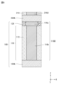
- FIG. 7 is a sectional view showing a composite component according to a second embodiment.
- FIG. 7 is an explanatory diagram illustrating a method for manufacturing a composite component device according to a second embodiment.
- FIG. 7 is an explanatory diagram illustrating a method for manufacturing a composite component device according to a second embodiment.
- FIG. 7 is an explanatory diagram illustrating a method for manufacturing a composite component device according to a second embodiment.
- FIG. 7 is an explanatory diagram illustrating a method for manufacturing a composite component device according to a second embodiment.
- FIG. 7 is an explanatory diagram illustrating a method for manufacturing a composite component device according to a second embodiment.
- FIG. 7 is an explanatory diagram illustrating a method for manufacturing a composite component device according to a second embodiment.
- FIG. 7 is an explanatory diagram illustrating a method for manufacturing a composite component device according to a second embodiment.
- FIG. 7 is an explanatory diagram illustrating a method for manufacturing a composite component device according to a second embodiment.
- FIG. 7 is an explanatory diagram illustrating a method for manufacturing a composite component device according to a second embodiment.
- FIG. 7 is an explanatory diagram illustrating a method for manufacturing a composite component device according to a second embodiment.
- FIG. 7 is an explanatory diagram illustrating a method for manufacturing a composite component device according to a second embodiment.
- FIG. 7 is an explanatory diagram illustrating a method for manufacturing a composite component device according to a second embodiment.
- FIG. 7 is an explanatory diagram illustrating a method for manufacturing a composite component device according to a second embodiment.
- FIG. 7 is an explanatory diagram illustrating a method for manufacturing a composite component device according to a second embodiment.
- FIG. 7 is an explanatory diagram illustrating a method for manufacturing a composite component device according to a second embodiment.
- FIG. 7 is an explanatory diagram illustrating a method for manufacturing a composite component device according to a second embodiment.
- FIG. 7 is an explanatory diagram illustrating a method for manufacturing a composite component device according to a second embodiment.
- FIG. 7 is a sectional view showing a composite component according to a third embodiment.
- FIG. 8 is an enlarged view of part D in FIG. 7.
- FIG. 7 is an explanatory diagram illustrating a method for manufacturing a composite component device according to a third embodiment.
- FIG. 7 is an explanatory diagram illustrating a method for manufacturing a composite component device according to a third embodiment.
- FIG. 7 is an explanatory diagram illustrating a method for manufacturing a composite component device according to a third embodiment.
- FIG. 7 is an explanatory diagram illustrating a method for manufacturing a composite component device according to a third embodiment.
- FIG. 7 is an explanatory diagram illustrating a method for manufacturing a composite component device according to a third embodiment.
- FIG. 7 is an explanatory diagram illustrating a method for manufacturing a composite component device according to a third embodiment.
- FIG. 7 is an explanatory diagram illustrating a method for manufacturing a composite component device according to a third embodiment.
- FIG. 7 is an explanatory diagram illustrating a method for manufacturing a composite component device according to a third embodiment.
- FIG. 7 is an explanatory diagram illustrating a method for manufacturing a composite component device according to a third embodiment.
- FIG. 7 is an explanatory diagram illustrating a method for manufacturing a composite component device according to a third embodiment.
- FIG. 7 is an explanatory diagram illustrating a method for manufacturing a composite component device according to a third embodiment.
- FIG. 7 is an explanatory diagram illustrating a method for manufacturing a composite component device according to a third embodiment.
- FIG. 2 is an explanatory diagram illustrating a method for manufacturing a composite component device according to a first embodiment.
- FIG. 2 is an explanatory diagram illustrating a method for manufacturing a composite component device according to a first embodiment.
- the composite component device according to the first embodiment includes two or more composite component layers.
- a composite component device including three composite component layers will be described as an example.
- the composite component device is A composite component device comprising two or more composite component layers having an electronic component layer and a rewiring layer provided on the electronic component layer, The two or more composite component layers are laminated in the thickness direction so that the electronic component layer and the rewiring layer are alternately arranged,
- the electronic component layer is one or more electronic components having an electronic component main body portion having a first surface perpendicular to the thickness direction and a second surface opposite to the first surface; and a plurality of component electrodes disposed on the first surface; component electrodes of one or more electronic components are electrically connected to the rewiring layer;
- the electronic component layer in the composite component layer adjacent to the rewiring layer of another composite component layer among the two or more composite component layers is It further includes an electronic component layer through-via electrically connected to a redistribution layer of another composite component layer.
- the composite component device according to the first embodiment can improve reliability and reduce the height. Although not bound by any particular theory, the reason is assumed to be as follows.
- component electrodes are electrically connected to the rewiring layer, and composite component layers are electrically connected to electronic component layer through-vias.
- This allows composite component devices to have shorter wiring lengths (especially the length of via wiring in the thickness direction of composite component devices) than when electrical connections are made using bumps (for example, solder bumps). Therefore, connection resistance can be reduced and reliability can be improved.
- the composite component device can eliminate the space caused by the bumps between the composite component layers, and can be made lower in height, compared to a case where bumps are used for electrical connection.
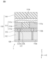
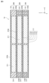
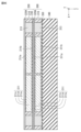
- FIG. 1 is a diagram schematically showing a cross section of a composite component device according to a first embodiment of the present disclosure.
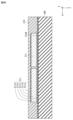
- FIG. 2 is an enlarged view of section A in FIG.
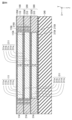
- FIG. 3 is an enlarged view of part B in FIG.
- the composite component device 1 includes three composite component layers 100, 200, and 300.
- the direction parallel to the thickness of the composite component device 1 is the Z direction
- the forward Z direction is the upper side
- the reverse Z direction is the lower side.
- the direction perpendicular to the Z direction is defined as the X direction.
- the direction perpendicular to the cross section of the composite component device 1 shown in FIG. 1 is defined as the Y direction.
- the composite component layers 100, 200, 300 each include an electronic component layer 110, 210, 310 and a rewiring layer 120, 220, 320 provided in the electronic component layer 110, 210, 310.
- the three composite component layers 100, 200, and 300 are laminated in the thickness direction so that the electronic component layers 110, 210, and 310 and the rewiring layers 120, 220, and 320 are alternately arranged.
- the composite component layer further includes an interlayer adhesive layer.
- the composite component layers 100, 200 further include interlayer adhesive layers 130, 230.
- the first composite component layer 100 Since the configurations of the second and third composite component layers 200 and 300 are almost the same as the configuration of the first composite component layer 100, the first composite component layer 100 will be described below as an example. However, the second and third composite component layers 200 and 300 may be referred to in terms of portions that are different from the first composite component layer 100.
- the third composite component layer 300 differs from the first and second composite component layers 100 and 200 in that it does not have an interlayer adhesive layer and a composite component layer through-via.
- the first electronic component layer 110 is bonded (bonded) to the first redistribution layer 120 on its lower surface, and the second composite component layer 200 is bonded to the first redistribution layer 120 on its upper surface via the first interlayer adhesive layer (first composite component adhesive layer) 130. It is adhered to the second redistribution layer 220 of.
- the first rewiring layer 120 and the second rewiring layer 220 are, for example, a sheet or a substrate of a multilayer wiring layer, as described later, and include, for example, a wiring (conductive wiring) 120b and an inorganic material (inorganic insulating material). ).
- the first electronic component layer 110 has one or more first electronic components 111 and a first electronic component layer through via 116, and further includes a first Si base layer 112, a first side wall portion 113, and a first resin sealing layer. It has a stop portion 114, a first electronic component adhesive layer 115, and a first Si through via 117.
- One or more first electronic components 111 are arranged within the first composite component layer 100.
- One or more first electronic components 111 have a first surface 111a perpendicular to the thickness direction and a second surface 111b opposite to the first surface 111a (first surface 111a and second surface 111b facing each other). It has a component body portion 111c, a plurality of first component electrodes 111d arranged on the first surface 111a, and a first insulating portion 111e arranged between the plurality of first component electrodes 111d.
- the first electronic component 111 is supported by the first Si base layer 112 via the first electronic component adhesive layer 115.
- the first electronic component 111 is sealed within the first composite component layer 100 by a first resin sealing portion 114 .
- the first component electrode 111d of the first electronic component 111 is electrically connected to the first rewiring layer 120 via the first Si through via 117.
- the first electronic components 111 may be of the same type or different types.
- the thickness of the first electronic component 111 is, for example, 80 to 120 ⁇ m.
- One or more first electronic components 111 are arranged such that the first surface 111a thereof is located on the first redistribution layer 120 side with respect to the second surface 111b. , disposed within the first composite component layer 100.
- the one or more second and third electronic components 211 and 311 are also all on the first surface thereof.
- 211a and 311a are arranged in the second and third composite component layers 200 and 300 so that they are located on the second and third redistribution layers 220 and 320 side with respect to the second surfaces 211b and 311b.
- These one or more electronic components 111, 211, and 311 are connected to rewiring layers 120, 220, and 320, respectively. In this way, since the composite component device 1 has simple wiring, not only two composite component layers but three or more composite component layers can be stacked.
- the one or more first electronic components 111 are, for example, electronic components in which one or more elements are integrated in a material similar to the material constituting the first Si base layer 112.
- the first electronic component 111 is, for example, an active component (more specifically, a CPU, a GPU, an LSI, etc.) and a passive component (more specifically, a capacitor, a resistor, an inductor, etc.).
- the first electronic component main body 111c includes, for example, ceramic or semiconductor material (more specifically, silicon, etc.).
- the first component electrode 111d is made of, for example, Cu, Ni, Sn, Al, or an alloy containing these as a conductive material.
- the conductive material is preferably the same material as the first Si through-via 117.
- the thickness of the first component electrode 111d is, for example, 1 ⁇ m to 30 ⁇ m, preferably 5 ⁇ m or less.
- the first component electrode 111d can be made as thin as 1 to 5 ⁇ m.
- the thickness of the first component electrode 111d can be, for example, 1/4 to 1/6 times the thickness of the first electronic component main body 111c.
- the first insulating portion 111e functions as a layer that electrically insulates between the first component electrodes 111d.
- the thickness of the first insulating portion 111e is, for example, 1 to 30 ⁇ m, preferably 5 ⁇ m or less.
- the first component electrode 111d can be made as thin as 1 to 5 ⁇ m.
- the thickness of the first insulating section 111e can be, for example, 1/4 to 1/6 times the thickness of the first electronic component main body section 111c.
- the thickness of the first insulating portion 111e may be the same as that of the first component electrode 111d, and in this case, the lower surface of the first insulating portion 111e and the lower surface of the first component electrode 111d are flush with each other.
- the first Si base layer 112 has a first main surface 112a and a second main surface 112b facing each other.
- the first Si base layer 112 supports one or more first electronic components 111 via the first electronic component adhesive layer 115 on the second main surface 112b, and supports the first redistribution layer 120 on the first main surface 112a.
- the first Si base layer 112 is substantially made of Si.
- substantially composed of Si as used herein means that the target member contains Si in a proportion of 99% by mass or more.
- the thickness of the first Si base layer 112 is, for example, 150 ⁇ m or less, preferably 50 ⁇ m or less, and more preferably 30 ⁇ m or less.
- the reason why the thickness of the first Si base layer 112 can be made extremely thin is that in the method for manufacturing the composite component device 1 described later, the first Si support 140 is bonded to the first Si base layer 112 to reinforce the strength. This is because even if the first Si base layer 112 is ground and thinned, damage (cracks, etc.) to the first Si base layer 112 due to insufficient strength is less likely to occur (see FIGS. 4E and 4F). The reinforcement of strength provided by the first Si support 140 makes it possible to manufacture the composite component device 1.
- the via wiring electrically connecting from the first component electrode 111d of one or more electronic components 111 to the first redistribution layer 120 (that is, the first The length of the through via 117) can be shortened. Thereby, the parasitic impedance due to the via wiring can be reduced, and the electrical characteristics of electronic equipment using the composite component device 1 can be improved.
- the first side wall portion 113 is arranged on the second main surface 112b of the first Si base layer 112 so as to surround one or more first electronic components 111.
- the first side wall portions 113 are arranged at both ends of the first composite component layer 100 so as to entirely surround one or more electronic components 111 .
- a first electronic component layer through-via 116 passes through the first side wall portion 113 .
- the first side wall portion 113 has a substantially rectangular shape in cross-sectional view, and is connected to the second redistribution layer 220 of the second composite component layer 200 via the first interlayer adhesive layer 130 on its upper surface, and is connected to the second redistribution layer 220 of the second composite component layer 200 on its lower surface. It is bonded to the first Si base layer 112 via the first electronic component adhesive layer 115.
- the thickness of the first side wall portion 113 is, for example, 90 to 130 ⁇ m.
- the first side wall portion 113 is, for example, substantially made of Si.
- the first resin sealing section 114 seals one or more first electronic components 111 .
- the resin sealing part 114 includes resin (for example, epoxy resin), and can integrate the plurality of (two or more) first electronic components 111 with the resin. Since the plurality of first electronic components 111 can be integrated with the resin, even if the two or more first electronic components 111 have different dimensions and shapes, the two or more first electronic components 111 can be integrated into the resin. 1 electronic component layer 110 . This allows design with a high degree of freedom, and allows two or more first electronic components 111 to be combined depending on the application. For example, the composite component device 1 can incorporate different types of first electronic components 111.
- the first electronic component adhesive layer 115 adheres one or more first electronic components 111 to the second main surface 112b of the first Si base layer 112.
- the thickness of the first electronic component adhesive layer 115 refers to the thickness in the Z direction from the lower surface of the first component electrode 111d to the second main surface 112b of the first Si base layer 112.
- the thickness of the first electronic component adhesive layer 115 is, for example, 4 to 6 ⁇ m.
- the electronic component layer in the composite component layer adjacent to the rewiring layer of another composite component layer among the two or more composite component layers has an electronic component layer through-via that electrically connects to the rewiring layer of the other composite component layer. It further has. That is, when the composite component layer is bonded to the rewiring layer of another composite component layer, it further includes an electronic component layer through-via electrically connected to the rewiring layer of the another composite component layer.
- the first electronic component layer 110 in the first composite component layer 100 adjacent to the second redistribution layer 220 of the second composite component layer 200 is electrically connected to the second redistribution layer 220 of the second composite component layer 200. It further includes a first electronic component layer through via 116 for connection.
- the first electronic component layer 110 since the first composite component layer 100 is connected to the second rewiring layer 220 of another second composite component layer 200, the first electronic component layer 110 is connected to the second rewiring layer 220 of the second composite component layer 200. It further includes a first electronic component through-layer via 116 electrically connected to layer 220.
- the second composite component layer 200 is connected to the third redistribution layer 320 of the third composite component layer 300
- the second electronic component layer 210 is electrically connected to the third redistribution layer 320 of the third composite component layer 300. It further includes a second electronic component layer through via 216 that is connected to the second electronic component layer.
- the third composite component layer 300 is not connected to the rewiring layer of another composite component layer, the third composite component layer 300 does not have an electronic component layer through-via.
- the first electronic component layer through via 116 penetrates the first electronic component layer 110 in the Z direction (more specifically, the first electronic component layer 113, the first electronic component adhesive layer 115, and the first Si base layer 112 in the Z direction). ), and also penetrates the first interlayer adhesive layer 130 .
- the first electronic component layer through-via 116 includes an adhesive layer conductive via 116 a that penetrates the first interlayer adhesive layer 130 , a side wall through-via 116 b that penetrates the first side wall 113 , and a first electronic component layer that penetrates the first electronic component adhesive layer 115 .
- a conductive via 116c that penetrates through the first Si base layer 112, and a through-Si via 116d that penetrates the first Si base layer 112.
- the adhesive layer conductive via 116a electrically connects the first electronic component layer through-via 116 and the second redistribution layer 220 of the second composite component layer 200.
- the cross-sectional area of the adhesive layer conductive via 116a (cross-sectional area in the XY plane) is larger than the cross-sectional area of the side wall through-via 116b. Therefore, the electrical connection between the first electronic component layer through-via 116 and the second redistribution layer 220 is improved, and the connection resistance between the first and second composite component layers 100 and 200 is reduced, which improves reliability. further improves.
- the first electronic component layer through-via 116 preferably consists essentially of copper.
- substantially made of copper (Cu) means that the target member contains copper in a proportion of 99% by mass or more.
- the first Si through via 117 penetrates the first Si base layer 112 (and the first electronic component adhesive layer 115) and connects the first component electrode 111d and the first redistribution layer 120. Connect electrically.
- the first Si through via 117 has a Si through via main body portion 117a and an extension portion 117b.
- the Si through-via main body portion 117a is electrically connected to the first redistribution layer 120 and penetrates through the first Si base layer 112.
- the extending portion 117b is electrically connected to the Si through-via main body portion 117a, extends from the second main surface 112b of the first Si base layer 112, penetrates the inside of the first electronic component adhesive layer 115, and connects to the first component electrode. It is electrically connected to 111d.
- the via wiring that electrically connects the first component electrode 111d to the first redistribution layer 120 is configured only from the first Si through-via 117, and therefore does not have (does not require) bumps (for example, solder bumps). ). Therefore, the composite component device 1 according to this embodiment can further reduce parasitic impedance due to via wiring. Furthermore, this improves the electronic characteristics of electronic equipment that uses the composite component device 1.
- the length of the via wiring (that is, the length of the first Si through-via 117 in the stacking direction) is, for example, 3 ⁇ m to 36 ⁇ m.
- solder bumps typically have a diameter of 100-150 ⁇ m.
- the first Si through-via 117 is approximately linear in the stacking direction.
- the cross-sectional shape of the first Si through-via 117 in the ZX plane is approximately rectangular in FIG. 2 .
- the cross-sectional shape of the first Si through-via 117 in the XY plane is, for example, a substantially circular shape, a substantially polygonal shape, or a substantially polygonal shape with rounded corners.
- the first redistribution layer 120 is formed on the first main surface 112a of the first Si base layer 112.
- the first rewiring layer 120 is a multilayer wiring layer.
- the first redistribution layer 120 includes a wiring (conductive wiring) 120b and a dielectric film 120a substantially made of an inorganic material (inorganic insulating material).
- the wiring 120b has a conductive via.
- the conductive via electrically connects wiring between different layers within the first redistribution layer 120.
- Wiring 120b includes a conductive material.
- the conductive material is, for example, Cu, Ag, and Au, and alloys containing them, and among these, Cu is preferred.
- the first redistribution layer 120 can have a plurality of layers, and includes, for example, two or more layers of wiring 120b and one or more layers of dielectric film 120a.
- the thickness of one layer of wiring 120b and one layer of dielectric film 120a constituting the first redistribution layer 120 is, for example, 1.5 ⁇ m to 5.0 ⁇ m.
- the thickness of the first redistribution layer 120 is the value obtained by multiplying the thickness of one of these layers (1.5 ⁇ m to 5.0 ⁇ m) by the total number of layers in the first redistribution layer 120 (unit: ⁇ m) becomes.
- the dielectric film 120a is substantially made of an inorganic material (inorganic insulating material) as an insulating material.
- substantially composed of an inorganic material means that the target member contains an inorganic material in a proportion of 99% by mass or more.
- inorganic insulating materials include silicon oxide (SiO 2 ) and silicon nitride (SiN, Si 3 N 4 ). If the dielectric film 120a is made of an inorganic insulating material, the wiring width can be reduced to about 1/10 of that of the dielectric film in the composite component device 1A according to the second embodiment, for example. This makes it possible to further reduce the size and height of the composite component device 1.
- the line and space (L/S) of the first redistribution layer 120 including the dielectric film 120a substantially made of an inorganic material is, for example, 1 ⁇ m/1 ⁇ m.
- the thickness of the dielectric film 120a is, for example, 0.1 to 2 ⁇ m.
- the dielectric film 120a may be a multi-component film containing two or more types of components.
- the multicomponent film may be a multilayer film in which a plurality of layers are formed for each component.
- the layer structure of the multilayer film is, in order from the first Si base layer 112 side, SiO 2 (thickness 0.25 ⁇ m)/Si 3 N 4 (thickness 0.1 ⁇ m)/SiO 2 (thickness 0.25 ⁇ m)/Si 3 N. 4 (thickness 0.1 ⁇ m).
- the first interlayer adhesive layer 130 adheres the first electronic component layer 110 and the second redistribution layer 220 of the second composite component layer 200 .
- the method for manufacturing the composite component device 1 according to the first embodiment includes, for example, An electronic method for bonding one or more electronic components to a Si base layer such that a plurality of component electrodes of the one or more electronic components are in contact with the bottom surface of the Si base layer having a lattice-shaped sidewall via an electronic component adhesive layer.
- an electronic component sealing step of sealing one or more electronic components with resin to form a resin sealing part a rewiring layer forming step of forming a rewiring layer to create a composite component layer
- Another composite component layer is formed by an electronic component adhesion process, an electronic component sealing process, and a rewiring layer forming process, and an electronic component layer through-via is formed on the side wall of the other composite component layer to add another composite component layer to the composite component layer.
- a lamination process of laminating composite component layers is performed at least once.
- the method for manufacturing the composite component device 1 according to the first embodiment is as follows: a Si base layer thinning step for thinning the Si base layer; A through hole forming step of forming a through hole in the thinned Si base layer and the electronic component adhesive layer to expose a part of the surface of the component electrode; The method further includes a through-Si via forming step of forming a through-Si via in the through-hole.
- the method for manufacturing the composite component device 1 according to the first embodiment further includes: a Si base layer preparation step for preparing a Si base layer; an insulating part forming step of forming an insulating part between component electrodes; a resin sealing part thinning process for thinning the resin sealing part; a Si support bonding step of bonding a Si support to an electronic component layer; a dielectric film forming step of forming a dielectric film having a predetermined pattern on the Si base layer;
- the method may also include a dicing step of dividing the method into individual pieces by dicing.
- FIGS. 10A to 10B and FIGS. 4A to 4V are diagrams for explaining a method for manufacturing the composite component device 1.
- FIG. The manufacturing method of the composite component device 1 according to the first embodiment includes an insulating part forming process, a Si base layer preparation process, an electronic component bonding process, an electronic component sealing process, a resin sealing part thinning process, Includes a Si support bonding process, a Si base layer thinning process, a dielectric film formation process, a through hole formation process, a Si through via formation process, a rewiring layer formation process, a lamination process, and a dicing process.
- a mother assembly in which composite component devices 1 are integrated is produced from the electronic component bonding process to the lamination process. Further, in this manufacturing method, the third composite component layer 300, the second composite component layer 200, and the first composite component layer 100 are manufactured in this order.
- a first insulating part 111e is formed between the first component electrodes 111d of the first electronic component 111.
- a coating film containing resin is formed, and a planarization process is performed to form the first insulating portion 111e.
- a solution containing a resin and a solvent is applied using a spin coating method to form a coating film.
- the lowest part of the coating film is made higher than the highest part of the first component electrode 111d. That is, the coating film is formed so that all of the plurality of first component electrodes 111d are completely buried in the coating film.
- the coating layer is dried to form the first insulating portion 111e.
- the first insulating portion 111e before the subsequent planarization process preferably completely covers the first component electrode 111d.
- the surfaces of the first component electrode 111d and the first insulating section 111e are ground and planarized using, for example, a surface planer and a grinder, and a first component electrode is formed between the first component electrodes 111d. 1 insulating section 111e is formed. As a result, the top surface of the first component electrode 111d is exposed, and the top surfaces of the first component electrode 111d and the first insulating section 111e are flush with each other.
- a third Si base layer 312 is prepared. Specifically, in the Si base layer preparation step, as shown in FIG. 4A, a Si wafer is prepared as the third Si base layer 312, and a third electronic component adhesive layer 315 (strictly speaking, An adhesive coating film) is formed, and the third side wall portion 313 is arranged. As a result, the third Si base layer 312 is formed, which has a rectangular bottom portion in plan view and sidewall portions arranged in a grid so as to surround the rectangular bottom portion.
- One or more third electronic components 311 are bonded to the recess (or depression, or cavity) surrounded by the bottom and side walls in an electronic component bonding process described later.
- the adhesive coating film is formed on the second main surface 312b of the third Si base layer 312. In this way, the third Si base layer 312 on which the coating film is formed is produced.
- the coating method is, for example, spin coating.
- the thickness of the coating film is controlled to be within the range of 10 ⁇ m from the thickness of the third component electrode 311d of the third electronic component 311 of one or more.
- the adhesive is, for example, a thermosetting resin.
- a thermosetting resin is, for example, a thermosetting resin containing a repeating unit derived from benzocyclobutene (BCB), and for example, 1,3-divinyl-1,1,3,3-tetramethyldisiloxane-bis. -Can be obtained by polymerizing benzocyclobutene (DVS-bis-BCB).
- a commercially available product is, for example, "CYCLOTENE" manufactured by Dow Chemical.
- the shape of the Si wafer may be a flat cylindrical shape when viewed from above, but is not limited to this.
- flatness means that the height (h) of the cylindrical shape is smaller than the outer diameter (diameter: 2r) (h/2r ⁇ 1).
- the thickness of the Si wafer is, for example, 775 ⁇ m (Si wafer diameter ⁇ 300 mm), 725 ⁇ m ( ⁇ 200 mm), 675 ⁇ m ( ⁇ 150 mm), and 525 ⁇ m ( ⁇ 100 mm).
- the Si base layer preparation step may be performed before the insulating portion forming step.
- Both the third Si base layer 312 and the third side wall portion 313 are substantially made of Si.
- a plurality of third component electrodes 311d of one or more third electronic components 311 are bonded to a third electronic component adhesive layer 315 on the bottom surface of the third Si base layer 312 having the third side wall portion 313 in a lattice shape.
- One or more third electronic components 311 are bonded to the third Si base layer 312 so as to be in contact therewith.
- the third component electrode 311d and the third insulating portion 311e are bonded to each other through the third electronic component adhesive layer 315 (strictly speaking, an adhesive coating film).
- one or more third electronic components 311 are arranged (mounted) on (the bottom surface of) the third Si base layer 312 so as to be in contact with (the bottom surface of) the third Si base layer 312 .
- the adhesive coating is cured to form a third electronic component adhesive layer 315.
- one or more third electronic components 311 are bonded onto the third Si base layer 312.
- the third electronic component 311 is placed on the coating film using a device equipped with a vacuum chamber. Specifically, an electronic component integrated wafer (a wafer in which one or more third electronic components 311 are integrated) is bonded to the third Si base layer 312 (the third Si base layer 312 having the third side wall portion 313). Pressure is applied in both directions along the stacking direction of the third electronic component 311 to heat it. Specifically, the third Si base layer 312 is set on the lower stage in the vacuum chamber of the apparatus. The third electronic component 311 is vacuum-suctioned (or vacuum-suctioned) to the upper stage in the vacuum chamber so that the third component electrode 311d of the third electronic component 311 faces the coating film.
- a recognition mark on the third Si base layer 312 is used to align the third Si base layer 312 with the electronic component integrated wafer.
- One or more third electronic components 311 are arranged on the coating film side of the third Si base layer 312. Pressure is applied in both directions along the direction in which the upper and lower stages face each other to heat the stage.
- the electronic component integrated wafer is bonded onto the third Si base layer 312 such that the third component electrode 311d and the third insulating portion 311e face the third Si base layer 312 via the third electronic component adhesive layer 315. .
- one or more third electronic components 311 are sealed with resin to form a third resin sealing portion 314 .
- a liquid resin is applied using a dispenser onto the third Si base layer 312 on which one or more third electronic components 311 are mounted. Thereafter, the applied liquid resin is molded using a compression molding device. The liquid resin is then cured using, for example, a hot air circulation oven. The heat treatment conditions for curing are, for example, 150° C. for 1 hour. As a result, a third resin sealing portion 314 is formed.
- the third resin sealing part 314 is thinned. Specifically, in the resin sealing part thinning step, as shown in FIG. 4D, the third resin sealing part 314 is ground and thinned using a Si wafer back grinder. In the electronic component thinning step, the surface of the third resin sealing portion 314 on the second surface 311b side of the third electronic component 311 is ground. It is preferable that the amount of grinding is as large as possible.
- the thickness of the third resin sealing portion 314 after thinning is, for example, 50 to 150 ⁇ m.
- the third resin sealing part 314 of the third electronic component layer 310 is ground, but it is also possible to grind one or more third electronic components 311. good. However, care should be taken not to damage the internal functional parts of the third electronic component 311.
- the functional parts are, for example, a dielectric and an electrode in the case of a capacitor, and wiring in the case of an inductor.
- a third Si support 340 is bonded to the third resin sealing portion 314.
- the Si wafer described in the Si base layer preparation step is separately prepared as the third Si support 340.
- an adhesive layer 350 (strictly speaking, an adhesive coating film) is formed on the third Si support 340 by the method described in the electronic component bonding process.
- the third resin sealing part 314 is bonded onto the third Si support 340 so that the ground surface of the third resin sealing part 314 comes into contact with the coating film, and heating is performed by applying pressure.
- the adhesive coating film is cured to form an adhesive layer 350, and the third Si support 340 is placed on the ground surface of the third resin sealing part 314 via the adhesive layer 350.
- the purpose of providing the third Si support 340 is to prevent the occurrence of adverse effects (more specifically, a decrease in strength, etc.) due to the thinner layer in the manufacturing process than in the past in the subsequent Si base layer thinning process. be.
- the third Si support 340 can be thinned before bonding, if necessary, from the viewpoint of improving processability. This is because a dielectric film will be formed using a semiconductor device in a subsequent process. For example, if the thickness of the third electronic component 311 is 150 ⁇ m, the Si wafer ( ⁇ 300 mm, typical thickness 775 ⁇ m) serving as the third Si support 340 is thinned to about 625 ⁇ m.
- the third Si base layer 312 is thinned. Specifically, in the Si base layer thinning process, as shown in FIG. 4F, the third Si base layer 312 is ground and thinned using the same method as the resin sealing part thinning process. to flatten the ground surface. In the Si base layer thinning process, since the third Si base layer 312 is thinned while being supported by the third Si support 340, the third Si base layer 312 can be effectively thinned. As a result, the method for manufacturing a composite component device 1 according to the present embodiment can manufacture a composite component device 1 that is an excellent electronic component module and has a reduced height and size.
- the amount of grinding is preferably as large as possible within a range that prevents the above disadvantages and maintains a certain strength, for example.
- the thickness of the third Si base layer 312 after thinning is preferably 3 ⁇ m or more.
- FIGS. 4G to 4I are enlarged views of a portion corresponding to section C in FIG. 4F.
- FIGS. 4J to 4M are diagrams mainly related to the formation of the third Si through via 317 and the third redistribution layer 320, for convenience, the third Si through via 317, the third redistribution layer 320, and the like are not formed. Please note that the area has expanded to occupy a large portion of the area.
- a chemical vapor deposition (CVD) method such as plasma-enhanced chemical vapor deposition (PECVD) is used to deposit the entire surface of the third Si base layer 312, as shown in FIG. 4G.
- a dielectric film (thickness: 0.1 to 0.2 ⁇ m) 320a is formed thereon.
- the dielectric film 320a may have one or more layers.
- SiO 2 : 0.25 ⁇ m/Si 3 N 4 0.1 ⁇ m/SiO 2 : 0.25 ⁇ m/Si 3 N 4 0 .1 ⁇ m.
- the surface of the third Si base layer 312 can be cleaned before forming the dielectric film 320a. Cleaning is, for example, wet cleaning and oxygen plasma ashing.
- the dielectric film 320a is patterned using a photolithography method.
- a photoresist film 360 is formed on the entire surface of the dielectric film 320a by spin coating a liquid resist.
- the photoresist film 360 is exposed to light through a mask corresponding to a predetermined pattern.
- the exposed photoresist film 360 is developed.
- the dielectric film 320a of the photoresist film 360 is selectively removed using RIE (Reactive Ion Etching). For example, when the above-mentioned four-layer dielectric film 320a is formed, two layers on the surface side of the dielectric film 320a (the surface side of the dielectric film 320a facing the third Si base layer 312 side) are selectively removed.
- RIE Reactive Ion Etching
- the photoresist film 360 is peeled off.
- a dielectric film 320a having a predetermined pattern is formed on the third Si base layer 312.
- the dielectric film 320a also functions as an insulating film that electrically insulates between two third Si through vias 317 shown in FIG. 4L, which will be described later.
- the first main surface 312a of the third Si base layer 312 may further include a mark layer.
- the mark layer can be detected with an infrared (IR) camera for alignment in photolithographic methods.
- through holes 312c and 315c are formed in the thinned third Si base layer 312 and third electronic component adhesive layer 315 to expose a part of the surface of the third component electrode 311d.
- a photoresist film 360 is formed over the entire surface.
- the photoresist film 360 is exposed through a mask corresponding to the pattern of the third Si through-via 317.
- the exposed photoresist film 360 is developed to form a photoresist film 360 having a predetermined pattern as shown in FIG. 4J. As shown in FIG.
- the third Si base layer 312 and the third electronic component adhesive layer 315 that are present in the Z direction from the opening 360a of the photoresist film 360 are selectively removed (etched). Etching is performed using, for example, RIE and laser irradiation. As a result, through holes 312c and 315c are formed, and the third component electrode 311d (part of the upper surface) is exposed.
- the through hole 315c of the third electronic component adhesive layer 315 in the ZX cross section has a substantially elliptical shape.
- the term "approximately elliptical shape” includes not only a strict elliptical shape but also a similar elliptical shape that takes into account actual variations in etching conditions during manufacturing.
- the material forming the third electronic component adhesive layer 315 is more easily etched than the material forming the third Si base layer 312. As a result, a substantially elliptical extending portion 317b is formed in the subsequent Si through-via forming step.
- the photoresist film 360 is removed.
- the etching means is preferably RIE. By using RIE as the etching means, the flatness of the exposed upper surface of the third component electrode 311d is improved, so that a good bond can be formed with the third Si through via 317 that will be formed later. Thereby, deterioration in electrical connectivity can be further suppressed.
- Si through-via formation process In the Si through-via forming step, a Si through-via is formed in the through hole. Specifically, in the through hole forming step, as shown in FIG. 4L, third Si through vias 317 are formed in the through holes 312c and 315c by electroplating. A third Si through via 317 is formed in the through holes 312c and 315c by electrolytic plating (more specifically, electrolytic Cu plating) using a dual damascene method (more specifically, a Cu dual damascene method). As a result, the third electronic component layer 310 is formed.
- a third rewiring layer 320 is formed to produce the third composite component layer 300.
- a dielectric film 320a and wiring 320b having a predetermined pattern are formed by the above-described photolithography method and etching, and the third rewiring layer 320 form.
- FIG. 4M shows a cross-sectional view of the third composite component layer 300 that includes FIG. 4M.
- FIG. 4M is an enlarged view of section C' in FIG. 4N.
- the lamination process In the lamination process, another composite component layer (first and second composite component layers 100, 200) is formed by the above-mentioned insulation part formation process to rewiring layer formation process, and an electronic component layer penetrating layer is formed in the other composite component layer. Vias 116 and 216 are formed to laminate the third composite component layer 300 with the other composite component layer. In this embodiment, the composite component layer is laminated twice. Specifically, first, in the lamination step, the second composite component layer 200 is laminated on the third composite component layer 300. The second composite component layer 200 is formed by the steps of forming an insulating part and forming a rewiring layer shown in FIGS. 4A to 4M.
- the second Si support 240 is removed from the second composite component layer 200 to which the second Si support 240 is bonded, and a second Si support is newly added to the second redistribution layer 220 of the second composite component layer 200, as shown in FIG. 4O.
- 240 is laminated.
- the second composite component layer 200 shown in FIG. 4O is bonded to the third composite component layer 300 shown in FIG. 4N using the second interlayer adhesive layer 230.
- the second Si support 240 is removed as shown in FIG. 4Q.
- a second electronic component layer through-via 216 is formed in the second composite component layer 200.
- the second electronic component layer through-via 216 can be formed by the same means as the Si through-via process described above.
- the second composite component layer 200 is laminated onto the third composite component layer 300.
- first composite component layer 100 is laminated.
- first composite component layer 100 is laminated on the second composite component layer 200 as shown in FIGS. 4A to 4P (see FIG. 4S).
- the first Si support 140 is removed as shown in FIG. 4T.
- first electronic component layer through-vias 116 are formed in the first composite component layer 100.
- the first electronic component layer through-via 116 can be formed by the same means as the Si through-via process described above.
- the first composite component layer 100 is further laminated.
- the composite component device according to the second embodiment has Si base layers 112, 212, 312, side wall portions 113, 213, 313, and Si through vias 117, 217, 317, compared to the composite component device according to the first embodiment. They are different in that they do not have a metal layer 370, and that electronic component adhesive layers 115, 215, 315 and electronic component layer through-vias 116, 216, 316 are different. This different configuration will be mainly explained below. Note that in the second embodiment, the same reference numerals as those in the first embodiment have the same configuration as those in the first embodiment, so the description thereof will be omitted in principle.
- FIG. 5 is a diagram schematically showing a cross section of a composite component device according to a second embodiment of the present disclosure. Similar to the first embodiment, the configurations of the second and third composite component layers 200 and 300 are almost the same as the first composite component layer 100, so the first composite component layer 100 will be mainly described below. However, matters that are different from the first composite component layer 100 may be referred to in the second and third composite component layers 200 and 300.
- the first electronic component layer 110 includes a first electronic component 111 and a first electronic component layer through-via 116A, and further includes a first resin sealing portion 114 and a first electronic component adhesive layer 115A.
- the first electronic component 111 is supported by the first redistribution layer 120A.
- the first component electrode 111d of the first electronic component 111 is directly electrically connected to (directly joined to) the first rewiring layer 120.
- the first electronic component adhesive layer 115A adheres the second surface 111b of the first electronic component 111 to the second redistribution layer 220A of the second composite component layer 200.
- the second electronic component adhesive layer 215A adheres the second surface 211b of the second electronic component 211 to the third rewiring layer 320 of the third composite component layer 300.
- the third electronic component adhesive layer 315A adheres the second surface 311b of the third electronic component 311 to the metal layer 370.
- the first electronic component layer through-via 116A is a columnar wiring (more specifically, a Cu pillar).
- the cross-sectional area of the first electronic component layer through via 116A in the XY plane is larger than that of the first electronic component layer through via 116 in the first embodiment.
- the cross-sectional diameter of the first electronic component layer through-via 116A in the XY plane is, for example, 35 to 100 ⁇ m.
- the number of first electronic component layer through-vias 116A is four in total in cross-sectional view, and two are arranged at each end of the first composite component layer 100.
- the cross-sectional area of the first electronic component layer through-via 116A in a plane perpendicular to the thickness direction of the composite component device 1A may increase from the second surface 111b of the first electronic component 111 toward the first surface 111a. That is, the shape of the first electronic component layer through-via 116A in the ZX cross section (ZX cross section shape) may be tapered with respect to the stacking direction of the composite component layers 100, 200, and 300. More specifically, the cross-sectional area (XY cross-sectional area) of the first electronic component layer through-via 116A in the XY plane may decrease from the second surface 111b toward the first surface 111a.
- the first rewiring layer 120A is directly connected to the first component electrode 111d. If the first redistribution layer 120A is directly connected to the first component electrode 111d, the length of the via wiring between the first redistribution layer 120A and the first component electrode 111d can be further reduced. Devices can be made smaller and lower in height, and the electrical resistance of via wiring can also be lowered.
- the first redistribution layer 120A includes a dielectric film substantially made of an organic material (organic insulating material) and wiring (conductive wiring).
- the expression that the dielectric film is substantially composed of an organic material means that the dielectric film contains an organic material in a proportion of 99% by mass or more.
- the dielectric film essentially consists of an organic insulating material as an insulating material. Examples of organic insulating materials include epoxy resin, silicone resin, polyester, polypropylene, polyimide, acrylonitrile-butadiene-styrene (ABS) resin, acrylonitrile-styrene (AS) resin, methacrylic resin, polyamide, fluororesin, liquid crystal polymer, and polyamide.
- the dielectric film is formed without using a method such as PECVD, so the cost is lower than that of the composite component device 1 according to the first embodiment. can be reduced.
- the line and space (L/S) of the first redistribution layer 120A including a dielectric film substantially made of an inorganic material is, for example, 10 ⁇ m/10 ⁇ m.
- the thickness of the dielectric film is, for example, 1 to 20 ⁇ m.
- the third composite component layer 300 has a metal layer 370.
- Metal layer 370 functions as an electromagnetic shield for composite component device 1A.
- the method for manufacturing the composite component device 1A according to the second embodiment includes, for example, an electronic component bonding step of bonding one or more electronic components to the Si support so that the second surface of the one or more electronic components contacts the Si support (Si support base material) via an electronic component adhesive layer; an electronic component sealing step of sealing one or more electronic components with resin to form a resin sealing part; a resin sealing part thinning step of thinning the resin sealing part to expose the entire surface of the component electrode; a rewiring layer forming step of forming a rewiring layer to create a composite component layer; An electronic component layer through via is formed on the composite component layer, and one or more electronic components are attached to the composite component layer such that the second surface of the one or more electronic components contacts the composite component layer via the electronic component adhesive layer.
- One or more electronic components are bonded and sealed with resin to form a resin sealing part, the resin sealing part is thinned to expose the entire surface of the component electrode, and a rewiring layer is formed to form a composite component layer. and a lamination step of laminating another composite component layer on the The lamination step is performed at least once.
- the method for manufacturing the composite component device 1A according to the second embodiment further includes: an insulating part forming step of forming an insulating part;
- the method may also include a dicing step of dividing the method into individual pieces by dicing.
- FIGS. 6A to 6O are diagrams for explaining a method of manufacturing the composite component device 1A.
- the manufacturing method of the composite component device 1A according to the second embodiment includes, in chronological order, an insulating part forming process, an electronic component bonding process, an electronic component sealing process, a resin sealing part thinning process, and a rewiring process. It includes a layer forming process, a laminating process, and a dicing process.
- the insulating part forming step see FIGS. 10A and 10B
- the electronic component sealing step see FIG. 6B
- the dicing step see FIG. 6O
- one or more third Si supports 340 are bonded to one or more third Si supports 340 such that the second surfaces 311b of one or more third electronic components 311 are in contact with the third Si supports 340 via the third electronic component adhesive layer 315A.
- the electronic component 311 is bonded. Specifically, in the electronic component bonding process, as shown in FIG.
- the second surface of the third electronic component 311 (the third insulating part 311e was formed in the same manner as the insulating part forming process of the first embodiment)
- a third electronic component adhesive layer 315A (strictly speaking, an adhesive coating film) is formed on the third electronic component adhesive layer 315A (strictly speaking, an adhesive coating film), and a third Si support 340 (strictly speaking, a metal layer 370 is arranged through the adhesive layer 350).
- One or more third electronic components 311 are arranged (mounted) on the third Si support 340).
- the third electronic component adhesive layer 315A is cured. As a result, one or more third electronic components 311 are bonded onto the third Si support 340.
- the third resin sealing part 314 is thinned to expose the entire surface of the third component electrode 311d.
- the third resin sealing part 314 is ground and thinned using a Si wafer back grinder. This exposes the entire surface of the third component electrode 311d. Note that in this step, part of the component electrode 311d and the third insulating part 311e may be ground.
- the third composite component layer 300 is produced by forming the third rewiring layer 320A. Specifically, in the rewiring layer forming step, as shown in FIG. 6D, a dielectric film and wiring having a predetermined pattern are formed using a photolithography method to form the third rewiring layer 320A. In the second embodiment, since a relatively expensive device such as PVCVD is not used to form the dielectric film, costs can be reduced.
- the second electronic component layer through-via 216A is formed on the third composite component layer 300, and the second surface 211b of one or more second electronic components 211 is bonded to the second electronic component layer 300.
- One or more second electronic components 211 are adhered to the third composite component layer 300 so as to be in contact with each other through the layer 215A, and the one or more second electronic components 211 are sealed with resin to form a second resin sealing part.
- the second resin sealing part 214 is thinned to expose the entire surface of the second component electrode 311d, and a second rewiring layer 220A is formed to add another composite component layer to the third composite component layer 300. (first and second composite component layers 100, 200) are laminated.
- the lamination process is performed twice.
- the second composite component layer 200 is laminated on the third composite component layer 300.
- a second electronic component layer through-via 216A is formed on the third composite component layer 300.
- a dry film resist (DFR) is laminated on (the entire surface of) the third redistribution layer 320A of the third composite component layer 300.
- An opening is formed through the DFR by photolithography.
- a second electronic component layer through-via 216A is formed in the opening by Cu via plating. Peel off the DER.
- the second electronic component layer penetrating via 216A is formed on the third composite component layer 300.
- the second surface 211b of one or more second electronic components 211 is brought into contact with the third composite component layer 300 via the second electronic component adhesive layer 215A. Then, one or more second electronic components 211 are bonded to the third composite component layer 300.
- one or more second electronic components 211 are sealed with resin to form a second resin sealing portion 214.
- the second resin sealing part 214 is thinned to expose the entire surface of the second component electrode 211d and the second insulating part 211e, as shown in FIG. 6H.
- a second rewiring layer 220A is formed as shown in FIG. 6I.
- the second composite component layer 200 is laminated on the third composite component layer 300.
- the first composite component layer 100 is laminated on the second composite component layer 200. Similar to the formation of the second composite component layer 200 in the above-described lamination process, the first composite component layer 100 is laminated on the second composite component layer 200, as shown in FIGS. 6J to 6N.
- a composite component device 1A according to the second embodiment is manufactured through the dicing process shown in FIG. 6O.
- the composite component device according to the third embodiment has Si base layers 112, 212, 312, electronic component adhesive layers 115, 215, 315, and Si through vias 117, 217, 317, compared to the composite component device according to the first embodiment.
- the difference is that the electronic component layer through-vias 116, 216, and 316 are different.
- This different configuration will be mainly explained below. Note that in the third embodiment, the same reference numerals as those in the first and second embodiments have the same configurations as in the first and second embodiments, so the description thereof will be omitted in principle.
- FIG. 7 is a diagram schematically showing a cross section of a composite component device according to a third embodiment of the present disclosure.
- FIG. 8 is an enlarged view of section D in FIG. 7.
- the first composite component layer 100 includes a first electronic component layer 110 and a rewiring layer 120A provided in the first electronic component layer 110.
- the first electronic component layer 110 includes a first electronic component 111 and a first electronic component layer through-via 116B, and further includes a first side wall portion 113 and a first resin sealing portion 114.
- the first electronic component layer through-via 116B penetrates the first side wall portion 113 of the first electronic component layer 110 in the Z direction, and also penetrates the first interlayer adhesive layer 130.
- the first electronic component layer through-via 116B includes an adhesive layer conductive via 116a that penetrates the first interlayer adhesive layer 130 and a sidewall through-via 116b that penetrates the first sidewall 113.
- the method for manufacturing the composite component device 1B according to the third embodiment includes, for example, An electronic method for bonding one or more electronic components to a Si base layer such that a plurality of component electrodes of the one or more electronic components are in contact with the bottom surface of the Si base layer having a lattice-shaped sidewall via an electronic component adhesive layer.
- a lamination process of laminating composite component layers; It consists of A lamination step is performed at least once.
- the manufacturing method of the composite component device 1B according to the third embodiment is as follows: The method further includes a Si base layer removal step of removing the Si base layer and the electronic component adhesive layer to expose the entire surface of the component electrode.
- the method for manufacturing the composite component device 1B according to the third embodiment further includes: a Si base layer preparation step for preparing a Si base layer; an insulating part forming step of forming an insulating part; a resin sealing part thinning process for thinning the resin sealing part; a Si support bonding step of bonding a Si support to an electronic component layer;
- the method may also include a dicing step of dividing the method into individual pieces by dicing.
- FIGS. 9A to 9J are diagrams for explaining the manufacturing method of the composite component device 1B.
- the manufacturing method of the composite component device 1B according to the third embodiment includes an insulating part forming step, a Si base layer preparation step, an electronic component bonding step, an electronic component sealing step, a resin sealing portion thinning step,
- the process includes a Si support bonding process, a Si base layer removal process, a rewiring layer formation process, a lamination process, and a dicing process.
- the insulating part forming step to the Si support bonding step are performed (see FIGS. 4A to 4E).
- Si base layer removal process In the Si base layer removal step, the third Si base layer 312 and the third electronic component adhesive layer 315 are removed to expose the entire surface of the third component electrode 111d. Specifically, in the Si base layer removal process, as shown in FIG. 9A, the third Si base layer 312 and the third electronic component adhesive layer are removed using the same means as the Si base layer thinning process in the first embodiment. 315 is removed.
- a third rewiring layer 320A is formed. Specifically, in the rewiring layer forming step, the third rewiring layer 320A is formed as shown in FIG. 9B using the same means as the rewiring layer forming step in the second embodiment. As a result, the third composite component layer 300 is formed.
- the lamination process is similar to the lamination process of the first embodiment, in which another composite component layer (first, second Composite component layers 100, 200) are formed, electronic component layer through-vias 116B, 216B are formed in the other composite component layer, and the other composite component layer is laminated on the third composite component layer 300.
- another composite component layer first, second Composite component layers 100, 200
- electronic component layer through-vias 116B, 216B are formed in the other composite component layer
- the other composite component layer is laminated on the third composite component layer 300.
- the composite component devices 1, 1A, and 1B are provided with three composite component layers, but the present invention is not limited thereto.
- a composite component device may include two or more composite component layers.
- the lamination step is performed once or three or more times in the method for manufacturing a composite component device.
- the wiring design is less likely to be complicated, and the composite component layers can be electrically connected easily. Therefore, even if three or more composite component layers are laminated, wiring can be easily formed. Therefore, in circuit design, there are fewer restrictions on the number and types of built-in electronic components, and the degree of freedom in design is high. Various circuit configurations become possible, and the range of applications to which it can be applied becomes wider.
- the composite component device had two electronic components of the same type in each composite component layer, but the invention is not limited to this.
- a composite component device may have different types of electronic components, and may have one or more electronic components in each composite component layer.
- a composite component device may have a different number of electronic components in each composite component layer. Therefore, in circuit design, there are fewer restrictions on the number and types of built-in electronic components, and the degree of freedom in design is high. Various circuit configurations become possible, and the range of applications to which it can be applied becomes wider.
- a composite component device comprising two or more composite component layers having an electronic component layer and a rewiring layer provided on the electronic component layer, The two or more composite component layers are laminated in the thickness direction so that the electronic component layer and the rewiring layer are alternately arranged,
- the electronic component layer is
- the electronic component has one or more electronic components having a first surface perpendicular to the thickness direction and a second surface opposite to the first surface, and a plurality of component electrodes disposed on the first surface.
- the component electrodes of the one or more electronic components are electrically connected to the rewiring layer
- the electronic component layer in the composite component layer adjacent to the rewiring layer of another composite component layer among the two or more composite component layers is:
- the composite component device further comprises an electronic component layer through-via electrically connected to the redistribution layer of the another composite component layer.
- the electronic component layer further includes a resin sealing part that seals the one or more electronic components.
- All electronic components included in the composite component device are arranged within the two or more composite component layers such that the first surface thereof is located on the rewiring layer side with respect to the second surface, ⁇ 1 > to ⁇ 3>.
- ⁇ 5> The electronic component layer is The composite component device according to any one of ⁇ 1> to ⁇ 4>, further comprising a side wall portion arranged to surround the one or more electronic components and through which the electronic component layer through-via passes.
- the electronic component layer is a Si-based layer supporting the one or more electronic components;
- ⁇ 7> The composite component device according to any one of ⁇ 1> to ⁇ 6>, wherein the rewiring layer has a dielectric film substantially made of an inorganic material.
- the composite component layer is bonded to the other composite component layer via an adhesive layer
- the electronic component layer through-via has a sidewall through-via that penetrates the sidewall and a conductive via that penetrates the adhesive layer,
- the conductive via electrically connects the electronic component layer through-via and the rewiring layer of the another composite component layer
- the composite component device according to ⁇ 5> wherein a cross-sectional area of the conductive via is larger than a cross-sectional area of the side wall through-via in a plane perpendicular to the thickness direction.
- ⁇ 9> The composite component device according to any one of ⁇ 1> to ⁇ 4>, wherein the rewiring layer is directly connected to the component electrode.
- ⁇ 10> The composite component device according to any one of ⁇ 1> to ⁇ 5> and ⁇ 9>, wherein the rewiring layer has a dielectric film substantially made of an organic material.
- ⁇ 11> The composite component device according to ⁇ 10>, wherein a cross-sectional area of the electronic component layer through-via in a plane perpendicular to the thickness direction increases from the second surface toward the first surface.
- a method for manufacturing the composite component device comprising:
- the electronic component layer of the composite component device is a side wall portion arranged to surround the one or more electronic components and through which the electronic component layer through-via passes; further comprising a resin sealing part that integrates the one or more electronic components,
- the one or more electronic components are attached to the Si base layer so that the plurality of component electrodes of the one or more electronic components are in contact with the bottom surface of the Si base layer having a grid-like side wall portion via an electronic component adhesive layer.
- a Si base layer thinning step of thinning the Si base layer a through-hole forming step of forming a through-hole in the thinned Si base layer and the electronic component adhesive layer to expose a part of the surface of the component electrode; further comprising a Si through via forming step of forming a Si through via in the through hole, The Si through via penetrates the Si base layer and the electronic component adhesive layer and electrically connects the rewiring layer and the component electrode of the electronic component,
- ⁇ 14> further comprising a Si base layer removing step of removing the Si base layer and the electronic component adhesive layer to expose the entire surface of the component electrode,
- a method for manufacturing the composite component device comprising:
- the electronic component layer of the composite component device further includes a resin sealing part that integrates the one or more electronic components
- the rewiring layer further includes a dielectric film that is in direct contact with the component electrode and is substantially made of an organic material, an electronic component bonding step of bonding the one or more electronic components to the Si support so that the second surface of the one or more electronic components contacts the Si support via an electronic component adhesive layer; an electronic component sealing step of sealing the one or more electronic components with a resin to form a resin sealing part; a resin sealing part thinning step of thinning the resin sealing part to expose the entire surface of the component electrode; a rewiring layer forming step of forming the rewiring layer to create a composite component layer;
- the electronic component layer through via is formed on the composite component layer, and the second surface of the one or more electronic components contacts the composite component layer via an electronic component adhesive layer.
- the composite component device according to the present disclosure can be installed and used in various electronic devices.
Abstract
L'invention concerne un dispositif de composant composite comprenant au moins deux couches de composant composite, dont une couche de composant électronique et une couche de recâblage disposée sur la couche de composant électronique, les au moins deux couches de composant composite étant stratifiées dans le sens de l'épaisseur de telle sorte que la couche de composant électronique et la couche de recâblage sont disposées en alternance ; la couche de composant électronique comprend un ou plusieurs composants électroniques ayant une partie de corps de composant électronique, qui a une première surface perpendiculaire au sens de l'épaisseur et une seconde surface opposée à la première surface, et une pluralité d'électrodes de composant, qui sont agencées sur la première surface ; les électrodes de composant du ou des composants électroniques sont électriquement connectées à la couche de recâblage ; et la couche de composant électronique dans la couche de composant composite qui est adjacente à la couche de recâblage, faisant partie des au moins deux couches de composant composite, comprend en outre un trou d'interconnexion de couche de composant électronique qui se connecte électriquement à la couche de recâblage d'une autre couche de composant composite.
Applications Claiming Priority (2)
| Application Number | Priority Date | Filing Date | Title |
|---|---|---|---|
| JP2022-122856 | 2022-08-01 | ||
| JP2022122856 | 2022-08-01 |
Publications (1)
| Publication Number | Publication Date |
|---|---|
| WO2024029138A1 true WO2024029138A1 (fr) | 2024-02-08 |
Family
ID=89849141
Family Applications (1)
| Application Number | Title | Priority Date | Filing Date |
|---|---|---|---|
| PCT/JP2023/015137 WO2024029138A1 (fr) | 2022-08-01 | 2023-04-14 | Dispositif de composant composite et son procédé de production |
Country Status (1)
| Country | Link |
|---|---|
| WO (1) | WO2024029138A1 (fr) |
Citations (6)
| Publication number | Priority date | Publication date | Assignee | Title |
|---|---|---|---|---|
| JP2001144218A (ja) * | 1999-11-17 | 2001-05-25 | Sony Corp | 半導体装置及び半導体装置の製造方法 |
| JP2007287803A (ja) * | 2006-04-13 | 2007-11-01 | Sony Corp | 三次元半導体パッケージ製造方法 |
| JP2010245259A (ja) * | 2009-04-06 | 2010-10-28 | Shinko Electric Ind Co Ltd | 電子装置及びその製造方法 |
| JP2012039090A (ja) * | 2010-07-15 | 2012-02-23 | Shinko Electric Ind Co Ltd | 半導体装置及びその製造方法 |
| WO2020261994A1 (fr) * | 2019-06-25 | 2020-12-30 | 株式会社村田製作所 | Composant composite et son procédé de fabrication |
| JP2021526309A (ja) * | 2018-06-14 | 2021-09-30 | インテル コーポレイション | 小型電子アセンブリ |
-
2023
- 2023-04-14 WO PCT/JP2023/015137 patent/WO2024029138A1/fr unknown
Patent Citations (6)
| Publication number | Priority date | Publication date | Assignee | Title |
|---|---|---|---|---|
| JP2001144218A (ja) * | 1999-11-17 | 2001-05-25 | Sony Corp | 半導体装置及び半導体装置の製造方法 |
| JP2007287803A (ja) * | 2006-04-13 | 2007-11-01 | Sony Corp | 三次元半導体パッケージ製造方法 |
| JP2010245259A (ja) * | 2009-04-06 | 2010-10-28 | Shinko Electric Ind Co Ltd | 電子装置及びその製造方法 |
| JP2012039090A (ja) * | 2010-07-15 | 2012-02-23 | Shinko Electric Ind Co Ltd | 半導体装置及びその製造方法 |
| JP2021526309A (ja) * | 2018-06-14 | 2021-09-30 | インテル コーポレイション | 小型電子アセンブリ |
| WO2020261994A1 (fr) * | 2019-06-25 | 2020-12-30 | 株式会社村田製作所 | Composant composite et son procédé de fabrication |
Similar Documents
| Publication | Publication Date | Title |
|---|---|---|
| KR100778597B1 (ko) | 적층 반도체 장치와 그 제조방법 | |
| US8810008B2 (en) | Semiconductor element-embedded substrate, and method of manufacturing the substrate | |
| US7042081B2 (en) | Semiconductor device having heat dissipation layer | |
| JP6342120B2 (ja) | 超薄埋設ダイモジュール及びその製造方法 | |
| US7075181B2 (en) | Semiconductor package having semiconductor constructing body and method of manufacturing the same | |
| TWI692817B (zh) | Info線圈結構及其製造方法 | |
| TWI528505B (zh) | 半導體結構及其製造方法 | |
| US20050161799A1 (en) | Semiconductor device having conducting portion of upper and lower conductive layers, and method of fabricating the same | |
| US9343498B2 (en) | Semiconductor device, imaging device and semiconductor device manufacturing method | |
| KR20210117186A (ko) | 반도체 디바이스 및 반도체 디바이스 제조 방법 | |
| TW201230222A (en) | Method of transferring and electrically joining a high density multilevel thin film to a circuitized and flexible organic substrate and associated devices | |
| US20180151542A1 (en) | Electronic packages with three-dimensional conductive planes, and methods for fabrication | |
| JP2011192726A (ja) | 電子装置および電子装置の製造方法 | |
| JP5589735B2 (ja) | 電子部品内蔵基板及びその製造方法 | |
| WO2024029138A1 (fr) | Dispositif de composant composite et son procédé de production | |
| JP2008135553A (ja) | 基板積層方法及び基板が積層された半導体装置 | |
| US20220020692A1 (en) | Composite component and method for manufacturing the same | |
| TWI420610B (zh) | 半導體裝置及其製造方法 | |
| JP4513302B2 (ja) | 半導体装置 | |
| JP2009246404A (ja) | 半導体装置の製造方法 | |
| JP2007116198A (ja) | 半導体装置 | |
| CN114171406A (zh) | 扇出式堆叠芯片的封装方法及封装结构 | |
| CN114171401A (zh) | 扇出式堆叠芯片的封装方法及封装结构 | |
| WO2022137657A1 (fr) | Composant composite et son procédé de fabrication | |
| WO2023153240A1 (fr) | Composant composite |
Legal Events
| Date | Code | Title | Description |
|---|---|---|---|
| 121 | Ep: the epo has been informed by wipo that ep was designated in this application |
Ref document number: 23849701 Country of ref document: EP Kind code of ref document: A1 |