WO2024029138A1 - Composite component device, and method for producing same - Google Patents
Composite component device, and method for producing same Download PDFInfo
- Publication number
- WO2024029138A1 WO2024029138A1 PCT/JP2023/015137 JP2023015137W WO2024029138A1 WO 2024029138 A1 WO2024029138 A1 WO 2024029138A1 JP 2023015137 W JP2023015137 W JP 2023015137W WO 2024029138 A1 WO2024029138 A1 WO 2024029138A1
- Authority
- WO
- WIPO (PCT)
- Prior art keywords
- layer
- composite component
- component
- electronic component
- electronic
- Prior art date
Links
- 239000002131 composite material Substances 0.000 title claims abstract description 401
- 238000004519 manufacturing process Methods 0.000 title claims description 98
- 239000010410 layer Substances 0.000 claims description 646
- 238000000034 method Methods 0.000 claims description 194
- 230000008569 process Effects 0.000 claims description 95
- 238000007789 sealing Methods 0.000 claims description 90
- 229920005989 resin Polymers 0.000 claims description 89
- 239000011347 resin Substances 0.000 claims description 89
- 239000012790 adhesive layer Substances 0.000 claims description 80
- 238000003475 lamination Methods 0.000 claims description 26
- 239000010949 copper Substances 0.000 claims description 15
- 238000010030 laminating Methods 0.000 claims description 12
- 229910010272 inorganic material Inorganic materials 0.000 claims description 11
- 239000011147 inorganic material Substances 0.000 claims description 11
- 229910052802 copper Inorganic materials 0.000 claims description 9
- 239000011368 organic material Substances 0.000 claims description 9
- RYGMFSIKBFXOCR-UHFFFAOYSA-N Copper Chemical compound [Cu] RYGMFSIKBFXOCR-UHFFFAOYSA-N 0.000 claims description 7
- 238000010586 diagram Methods 0.000 description 56
- 238000000576 coating method Methods 0.000 description 20
- 239000011248 coating agent Substances 0.000 description 19
- 230000015572 biosynthetic process Effects 0.000 description 15
- 239000011229 interlayer Substances 0.000 description 13
- 239000011810 insulating material Substances 0.000 description 12
- 239000000853 adhesive Substances 0.000 description 11
- 230000001070 adhesive effect Effects 0.000 description 11
- 229920002120 photoresistant polymer Polymers 0.000 description 11
- 238000002360 preparation method Methods 0.000 description 9
- 239000000463 material Substances 0.000 description 7
- 239000002184 metal Substances 0.000 description 6
- 229910052751 metal Inorganic materials 0.000 description 6
- 229910004298 SiO 2 Inorganic materials 0.000 description 5
- 239000004020 conductor Substances 0.000 description 5
- 238000005530 etching Methods 0.000 description 5
- 238000001020 plasma etching Methods 0.000 description 5
- 229910000679 solder Inorganic materials 0.000 description 5
- 239000007788 liquid Substances 0.000 description 4
- 238000000206 photolithography Methods 0.000 description 4
- UMIVXZPTRXBADB-UHFFFAOYSA-N benzocyclobutene Chemical compound C1=CC=C2CCC2=C1 UMIVXZPTRXBADB-UHFFFAOYSA-N 0.000 description 3
- 238000000623 plasma-assisted chemical vapour deposition Methods 0.000 description 3
- 238000004528 spin coating Methods 0.000 description 3
- 229920001187 thermosetting polymer Polymers 0.000 description 3
- CFAKWWQIUFSQFU-UHFFFAOYSA-N 2-hydroxy-3-methylcyclopent-2-en-1-one Chemical compound CC1=C(O)C(=O)CC1 CFAKWWQIUFSQFU-UHFFFAOYSA-N 0.000 description 2
- 239000004952 Polyamide Substances 0.000 description 2
- 229920001893 acrylonitrile styrene Polymers 0.000 description 2
- 229910045601 alloy Inorganic materials 0.000 description 2
- 239000000956 alloy Substances 0.000 description 2
- 239000003990 capacitor Substances 0.000 description 2
- 238000005229 chemical vapour deposition Methods 0.000 description 2
- 238000004140 cleaning Methods 0.000 description 2
- 230000009977 dual effect Effects 0.000 description 2
- 238000009713 electroplating Methods 0.000 description 2
- 239000003822 epoxy resin Substances 0.000 description 2
- 238000000227 grinding Methods 0.000 description 2
- 238000010438 heat treatment Methods 0.000 description 2
- 238000005259 measurement Methods 0.000 description 2
- 230000003071 parasitic effect Effects 0.000 description 2
- 230000000149 penetrating effect Effects 0.000 description 2
- 238000007747 plating Methods 0.000 description 2
- 229920002647 polyamide Polymers 0.000 description 2
- 229920000647 polyepoxide Polymers 0.000 description 2
- -1 polypropylene Polymers 0.000 description 2
- SCUZVMOVTVSBLE-UHFFFAOYSA-N prop-2-enenitrile;styrene Chemical compound C=CC#N.C=CC1=CC=CC=C1 SCUZVMOVTVSBLE-UHFFFAOYSA-N 0.000 description 2
- 239000004065 semiconductor Substances 0.000 description 2
- 239000001837 2-hydroxy-3-methylcyclopent-2-en-1-one Substances 0.000 description 1
- WSQZNZLOZXSBHA-UHFFFAOYSA-N 3,8-dioxabicyclo[8.2.2]tetradeca-1(12),10,13-triene-2,9-dione Chemical compound O=C1OCCCCOC(=O)C2=CC=C1C=C2 WSQZNZLOZXSBHA-UHFFFAOYSA-N 0.000 description 1
- 229920000106 Liquid crystal polymer Polymers 0.000 description 1
- 239000004977 Liquid-crystal polymers (LCPs) Substances 0.000 description 1
- 239000004642 Polyimide Substances 0.000 description 1
- 239000004743 Polypropylene Substances 0.000 description 1
- 229910052581 Si3N4 Inorganic materials 0.000 description 1
- VYPSYNLAJGMNEJ-UHFFFAOYSA-N Silicium dioxide Chemical compound O=[Si]=O VYPSYNLAJGMNEJ-UHFFFAOYSA-N 0.000 description 1
- 229920000122 acrylonitrile butadiene styrene Polymers 0.000 description 1
- 239000004676 acrylonitrile butadiene styrene Substances 0.000 description 1
- 230000002411 adverse Effects 0.000 description 1
- 229910052782 aluminium Inorganic materials 0.000 description 1
- 238000004380 ashing Methods 0.000 description 1
- QVGXLLKOCUKJST-UHFFFAOYSA-N atomic oxygen Chemical compound [O] QVGXLLKOCUKJST-UHFFFAOYSA-N 0.000 description 1
- 239000000919 ceramic Substances 0.000 description 1
- 239000011247 coating layer Substances 0.000 description 1
- 238000000748 compression moulding Methods 0.000 description 1
- 230000006866 deterioration Effects 0.000 description 1
- 230000000694 effects Effects 0.000 description 1
- 229910052737 gold Inorganic materials 0.000 description 1
- 239000010931 gold Substances 0.000 description 1
- 238000009413 insulation Methods 0.000 description 1
- 230000010534 mechanism of action Effects 0.000 description 1
- 239000000113 methacrylic resin Substances 0.000 description 1
- 229910052759 nickel Inorganic materials 0.000 description 1
- 229910052760 oxygen Inorganic materials 0.000 description 1
- 239000001301 oxygen Substances 0.000 description 1
- 229920000515 polycarbonate Polymers 0.000 description 1
- 239000004417 polycarbonate Substances 0.000 description 1
- 229920000728 polyester Polymers 0.000 description 1
- 229920001721 polyimide Polymers 0.000 description 1
- 230000000379 polymerizing effect Effects 0.000 description 1
- 229920001155 polypropylene Polymers 0.000 description 1
- 238000003825 pressing Methods 0.000 description 1
- 230000009467 reduction Effects 0.000 description 1
- 230000002787 reinforcement Effects 0.000 description 1
- 238000001878 scanning electron micrograph Methods 0.000 description 1
- 229910052710 silicon Inorganic materials 0.000 description 1
- 239000010703 silicon Substances 0.000 description 1
- HQVNEWCFYHHQES-UHFFFAOYSA-N silicon nitride Chemical compound N12[Si]34N5[Si]62N3[Si]51N64 HQVNEWCFYHHQES-UHFFFAOYSA-N 0.000 description 1
- 229910052814 silicon oxide Inorganic materials 0.000 description 1
- 229920002050 silicone resin Polymers 0.000 description 1
- 229910052709 silver Inorganic materials 0.000 description 1
- 239000010944 silver (metal) Substances 0.000 description 1
- 239000002904 solvent Substances 0.000 description 1
- 239000000126 substance Substances 0.000 description 1
- 239000000758 substrate Substances 0.000 description 1
- 229910052718 tin Inorganic materials 0.000 description 1
Images


Classifications
-
- H—ELECTRICITY
- H01—ELECTRIC ELEMENTS
- H01L—SEMICONDUCTOR DEVICES NOT COVERED BY CLASS H10
- H01L23/00—Details of semiconductor or other solid state devices
- H01L23/32—Holders for supporting the complete device in operation, i.e. detachable fixtures
-
- H—ELECTRICITY
- H01—ELECTRIC ELEMENTS
- H01L—SEMICONDUCTOR DEVICES NOT COVERED BY CLASS H10
- H01L25/00—Assemblies consisting of a plurality of individual semiconductor or other solid state devices ; Multistep manufacturing processes thereof
- H01L25/03—Assemblies consisting of a plurality of individual semiconductor or other solid state devices ; Multistep manufacturing processes thereof all the devices being of a type provided for in the same subgroup of groups H01L27/00 - H01L33/00, or in a single subclass of H10K, H10N, e.g. assemblies of rectifier diodes
- H01L25/04—Assemblies consisting of a plurality of individual semiconductor or other solid state devices ; Multistep manufacturing processes thereof all the devices being of a type provided for in the same subgroup of groups H01L27/00 - H01L33/00, or in a single subclass of H10K, H10N, e.g. assemblies of rectifier diodes the devices not having separate containers
- H01L25/065—Assemblies consisting of a plurality of individual semiconductor or other solid state devices ; Multistep manufacturing processes thereof all the devices being of a type provided for in the same subgroup of groups H01L27/00 - H01L33/00, or in a single subclass of H10K, H10N, e.g. assemblies of rectifier diodes the devices not having separate containers the devices being of a type provided for in group H01L27/00
-
- H—ELECTRICITY
- H01—ELECTRIC ELEMENTS
- H01L—SEMICONDUCTOR DEVICES NOT COVERED BY CLASS H10
- H01L25/00—Assemblies consisting of a plurality of individual semiconductor or other solid state devices ; Multistep manufacturing processes thereof
- H01L25/03—Assemblies consisting of a plurality of individual semiconductor or other solid state devices ; Multistep manufacturing processes thereof all the devices being of a type provided for in the same subgroup of groups H01L27/00 - H01L33/00, or in a single subclass of H10K, H10N, e.g. assemblies of rectifier diodes
- H01L25/04—Assemblies consisting of a plurality of individual semiconductor or other solid state devices ; Multistep manufacturing processes thereof all the devices being of a type provided for in the same subgroup of groups H01L27/00 - H01L33/00, or in a single subclass of H10K, H10N, e.g. assemblies of rectifier diodes the devices not having separate containers
- H01L25/07—Assemblies consisting of a plurality of individual semiconductor or other solid state devices ; Multistep manufacturing processes thereof all the devices being of a type provided for in the same subgroup of groups H01L27/00 - H01L33/00, or in a single subclass of H10K, H10N, e.g. assemblies of rectifier diodes the devices not having separate containers the devices being of a type provided for in group H01L29/00
-
- H—ELECTRICITY
- H01—ELECTRIC ELEMENTS
- H01L—SEMICONDUCTOR DEVICES NOT COVERED BY CLASS H10
- H01L25/00—Assemblies consisting of a plurality of individual semiconductor or other solid state devices ; Multistep manufacturing processes thereof
- H01L25/03—Assemblies consisting of a plurality of individual semiconductor or other solid state devices ; Multistep manufacturing processes thereof all the devices being of a type provided for in the same subgroup of groups H01L27/00 - H01L33/00, or in a single subclass of H10K, H10N, e.g. assemblies of rectifier diodes
- H01L25/10—Assemblies consisting of a plurality of individual semiconductor or other solid state devices ; Multistep manufacturing processes thereof all the devices being of a type provided for in the same subgroup of groups H01L27/00 - H01L33/00, or in a single subclass of H10K, H10N, e.g. assemblies of rectifier diodes the devices having separate containers
- H01L25/11—Assemblies consisting of a plurality of individual semiconductor or other solid state devices ; Multistep manufacturing processes thereof all the devices being of a type provided for in the same subgroup of groups H01L27/00 - H01L33/00, or in a single subclass of H10K, H10N, e.g. assemblies of rectifier diodes the devices having separate containers the devices being of a type provided for in group H01L29/00
-
- H—ELECTRICITY
- H01—ELECTRIC ELEMENTS
- H01L—SEMICONDUCTOR DEVICES NOT COVERED BY CLASS H10
- H01L25/00—Assemblies consisting of a plurality of individual semiconductor or other solid state devices ; Multistep manufacturing processes thereof
- H01L25/18—Assemblies consisting of a plurality of individual semiconductor or other solid state devices ; Multistep manufacturing processes thereof the devices being of types provided for in two or more different subgroups of the same main group of groups H01L27/00 - H01L33/00, or in a single subclass of H10K, H10N
-
- H—ELECTRICITY
- H05—ELECTRIC TECHNIQUES NOT OTHERWISE PROVIDED FOR
- H05K—PRINTED CIRCUITS; CASINGS OR CONSTRUCTIONAL DETAILS OF ELECTRIC APPARATUS; MANUFACTURE OF ASSEMBLAGES OF ELECTRICAL COMPONENTS
- H05K1/00—Printed circuits
- H05K1/02—Details
- H05K1/03—Use of materials for the substrate
Definitions
- the present disclosure relates to a composite component device and a method for manufacturing the same.
- FIG. 4F Japanese Patent Application Publication No. 2019-125779
- This device (400F) includes a rewiring layer (306), a first mold layer (316) placed on the rewiring layer (306), and a second mold layer (316) placed on the first mold layer (316). layer (326). Dies (318, 320) encapsulated within the second mold layer (326) are connected via electrical connections (312) to a bridge die (310) encapsulated within the first mold layer (316). and is connected to the redistribution layer (306) via the electrical connection portion (314).
- the present inventor found that the above-mentioned device has the following problem. That is, the die, bridge die, and wiring layer are connected via balls (bumps). Therefore, the connection resistance is relatively high, and there is a risk that reliability may be reduced due to cracks in the bumps or the like. Furthermore, there is a possibility that a space is formed within the device due to the bumps used during manufacturing, which may hinder the reduction in height.
- an object of the present disclosure is to provide a composite component device that can improve reliability and reduce the height.
- the present inventor has made extensive studies, and has provided a composite component device having two or more composite component layers each having an electronic component layer and a rewiring layer provided in the electronic component layer. It has been found that electrical connections between electronic components and redistribution layers and between two or more composite component layers can be made without using solder bumps. Based on such technical knowledge, we have come up with the present disclosure in which component electrodes are electrically connected to rewiring layers, and composite component layers are electrically connected to electronic component layer through-vias. That is, the present disclosure includes the following embodiments.
- a composite component device that is one aspect of the present disclosure includes: A composite component device comprising two or more composite component layers having an electronic component layer and a rewiring layer provided on the electronic component layer, The two or more composite component layers are laminated in the thickness direction so that the electronic component layer and the rewiring layer are alternately arranged,
- the electronic component layer is The electronic component has one or more electronic components having a first surface perpendicular to the thickness direction and a second surface opposite to the first surface, and a plurality of component electrodes disposed on the first surface.
- the component electrodes of the one or more electronic components are electrically connected to the rewiring layer
- the electronic component layer in the composite component layer adjacent to the rewiring layer of another composite component layer among the two or more composite component layers is:
- the electronic component layer further includes an electronic component layer through-via electrically connected to the redistribution layer of the another composite component layer.
- the component electrodes are electrically connected to the rewiring layer, and the composite component layers are electrically connected to the electronic component layer through-vias.
- This allows composite component devices to have shorter wiring lengths (especially the length of via wiring in the thickness direction of composite component devices) than when electrical connections are made using bumps (for example, solder bumps). Therefore, connection resistance can be reduced and reliability can be improved.
- the composite component device can eliminate the space caused by the bumps between the composite component layers, and can be made lower in height, compared to a case where bumps are used for electrical connection.
- reliability can be increased and the height can be reduced.
- FIG. 1 is a cross-sectional view showing a composite component according to a first embodiment.
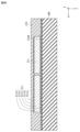
- 2 is an enlarged view of part A in FIG. 1.
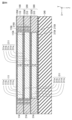
- FIG. 2 is an enlarged view of part B in FIG. 1.
- FIG. 2 is an explanatory diagram illustrating a method for manufacturing a composite component device according to a first embodiment.
- FIG. 2 is an explanatory diagram illustrating a method for manufacturing a composite component device according to a first embodiment.
- FIG. 2 is an explanatory diagram illustrating a method for manufacturing a composite component device according to a first embodiment.
- FIG. 2 is an explanatory diagram illustrating a method for manufacturing a composite component device according to a first embodiment.
- FIG. 2 is an explanatory diagram illustrating a method for manufacturing a composite component device according to a first embodiment.
- FIG. 2 is an explanatory diagram illustrating a method for manufacturing a composite component device according to a first embodiment.
- FIG. 2 is an explanatory diagram illustrating a method for manufacturing a composite component device according to a first embodiment.
- FIG. 2 is an explanatory diagram illustrating a method for manufacturing a composite component device according to a first embodiment.
- FIG. 2 is an explanatory diagram illustrating a method for manufacturing a composite component device according to a first embodiment.
- FIG. 2 is an explanatory diagram illustrating a method for manufacturing a composite component device according to a first embodiment.
- FIG. 2 is an explanatory diagram illustrating a method for manufacturing a composite component device according to a first embodiment.
- FIG. 2 is an explanatory diagram illustrating a method for manufacturing a composite component device according to a first embodiment.
- FIG. 2 is an explanatory diagram illustrating a method for manufacturing a composite component device according to a first embodiment.
- FIG. 2 is an explanatory diagram illustrating a method for manufacturing a composite component device according to a first embodiment.
- FIG. 2 is an explanatory diagram illustrating a method for manufacturing a composite component device according to a first embodiment.
- FIG. 2 is an explanatory diagram illustrating a method for manufacturing a composite component device according to a first embodiment.
- FIG. 2 is an explanatory diagram illustrating a method for manufacturing a composite component device according to a first embodiment.
- FIG. 2 is an explanatory diagram illustrating a method for manufacturing a composite component device according to a first embodiment.
- FIG. 2 is an explanatory diagram illustrating a method for manufacturing a composite component device according to a first embodiment.
- FIG. 2 is an explanatory diagram illustrating a method for manufacturing a composite component device according to a first embodiment.
- FIG. 2 is an explanatory diagram illustrating a method for manufacturing a composite component device according to a first embodiment.
- FIG. 2 is an explanatory diagram illustrating a method for manufacturing a composite component device according to a first embodiment.
- FIG. 2 is an explanatory diagram illustrating a method for manufacturing a composite component device according to a first embodiment.
- FIG. 2 is an explanatory diagram illustrating a method for manufacturing a composite component device according to a first embodiment.
- FIG. 2 is an explanatory diagram illustrating a method for manufacturing a composite component device according to a first embodiment.
- FIG. 7 is a sectional view showing a composite component according to a second embodiment.
- FIG. 7 is an explanatory diagram illustrating a method for manufacturing a composite component device according to a second embodiment.
- FIG. 7 is an explanatory diagram illustrating a method for manufacturing a composite component device according to a second embodiment.
- FIG. 7 is an explanatory diagram illustrating a method for manufacturing a composite component device according to a second embodiment.
- FIG. 7 is an explanatory diagram illustrating a method for manufacturing a composite component device according to a second embodiment.
- FIG. 7 is an explanatory diagram illustrating a method for manufacturing a composite component device according to a second embodiment.
- FIG. 7 is an explanatory diagram illustrating a method for manufacturing a composite component device according to a second embodiment.
- FIG. 7 is an explanatory diagram illustrating a method for manufacturing a composite component device according to a second embodiment.
- FIG. 7 is an explanatory diagram illustrating a method for manufacturing a composite component device according to a second embodiment.
- FIG. 7 is an explanatory diagram illustrating a method for manufacturing a composite component device according to a second embodiment.
- FIG. 7 is an explanatory diagram illustrating a method for manufacturing a composite component device according to a second embodiment.
- FIG. 7 is an explanatory diagram illustrating a method for manufacturing a composite component device according to a second embodiment.
- FIG. 7 is an explanatory diagram illustrating a method for manufacturing a composite component device according to a second embodiment.
- FIG. 7 is an explanatory diagram illustrating a method for manufacturing a composite component device according to a second embodiment.
- FIG. 7 is an explanatory diagram illustrating a method for manufacturing a composite component device according to a second embodiment.
- FIG. 7 is an explanatory diagram illustrating a method for manufacturing a composite component device according to a second embodiment.
- FIG. 7 is an explanatory diagram illustrating a method for manufacturing a composite component device according to a second embodiment.
- FIG. 7 is an explanatory diagram illustrating a method for manufacturing a composite component device according to a second embodiment.
- FIG. 7 is a sectional view showing a composite component according to a third embodiment.
- FIG. 8 is an enlarged view of part D in FIG. 7.
- FIG. 7 is an explanatory diagram illustrating a method for manufacturing a composite component device according to a third embodiment.
- FIG. 7 is an explanatory diagram illustrating a method for manufacturing a composite component device according to a third embodiment.
- FIG. 7 is an explanatory diagram illustrating a method for manufacturing a composite component device according to a third embodiment.
- FIG. 7 is an explanatory diagram illustrating a method for manufacturing a composite component device according to a third embodiment.
- FIG. 7 is an explanatory diagram illustrating a method for manufacturing a composite component device according to a third embodiment.
- FIG. 7 is an explanatory diagram illustrating a method for manufacturing a composite component device according to a third embodiment.
- FIG. 7 is an explanatory diagram illustrating a method for manufacturing a composite component device according to a third embodiment.
- FIG. 7 is an explanatory diagram illustrating a method for manufacturing a composite component device according to a third embodiment.
- FIG. 7 is an explanatory diagram illustrating a method for manufacturing a composite component device according to a third embodiment.
- FIG. 7 is an explanatory diagram illustrating a method for manufacturing a composite component device according to a third embodiment.
- FIG. 7 is an explanatory diagram illustrating a method for manufacturing a composite component device according to a third embodiment.
- FIG. 7 is an explanatory diagram illustrating a method for manufacturing a composite component device according to a third embodiment.
- FIG. 2 is an explanatory diagram illustrating a method for manufacturing a composite component device according to a first embodiment.
- FIG. 2 is an explanatory diagram illustrating a method for manufacturing a composite component device according to a first embodiment.
- the composite component device according to the first embodiment includes two or more composite component layers.
- a composite component device including three composite component layers will be described as an example.
- the composite component device is A composite component device comprising two or more composite component layers having an electronic component layer and a rewiring layer provided on the electronic component layer, The two or more composite component layers are laminated in the thickness direction so that the electronic component layer and the rewiring layer are alternately arranged,
- the electronic component layer is one or more electronic components having an electronic component main body portion having a first surface perpendicular to the thickness direction and a second surface opposite to the first surface; and a plurality of component electrodes disposed on the first surface; component electrodes of one or more electronic components are electrically connected to the rewiring layer;
- the electronic component layer in the composite component layer adjacent to the rewiring layer of another composite component layer among the two or more composite component layers is It further includes an electronic component layer through-via electrically connected to a redistribution layer of another composite component layer.
- the composite component device according to the first embodiment can improve reliability and reduce the height. Although not bound by any particular theory, the reason is assumed to be as follows.
- component electrodes are electrically connected to the rewiring layer, and composite component layers are electrically connected to electronic component layer through-vias.
- This allows composite component devices to have shorter wiring lengths (especially the length of via wiring in the thickness direction of composite component devices) than when electrical connections are made using bumps (for example, solder bumps). Therefore, connection resistance can be reduced and reliability can be improved.
- the composite component device can eliminate the space caused by the bumps between the composite component layers, and can be made lower in height, compared to a case where bumps are used for electrical connection.
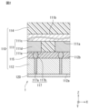
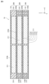
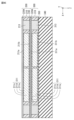
- FIG. 1 is a diagram schematically showing a cross section of a composite component device according to a first embodiment of the present disclosure.
- FIG. 2 is an enlarged view of section A in FIG.
- FIG. 3 is an enlarged view of part B in FIG.
- the composite component device 1 includes three composite component layers 100, 200, and 300.
- the direction parallel to the thickness of the composite component device 1 is the Z direction
- the forward Z direction is the upper side
- the reverse Z direction is the lower side.
- the direction perpendicular to the Z direction is defined as the X direction.
- the direction perpendicular to the cross section of the composite component device 1 shown in FIG. 1 is defined as the Y direction.
- the composite component layers 100, 200, 300 each include an electronic component layer 110, 210, 310 and a rewiring layer 120, 220, 320 provided in the electronic component layer 110, 210, 310.
- the three composite component layers 100, 200, and 300 are laminated in the thickness direction so that the electronic component layers 110, 210, and 310 and the rewiring layers 120, 220, and 320 are alternately arranged.
- the composite component layer further includes an interlayer adhesive layer.
- the composite component layers 100, 200 further include interlayer adhesive layers 130, 230.
- the first composite component layer 100 Since the configurations of the second and third composite component layers 200 and 300 are almost the same as the configuration of the first composite component layer 100, the first composite component layer 100 will be described below as an example. However, the second and third composite component layers 200 and 300 may be referred to in terms of portions that are different from the first composite component layer 100.
- the third composite component layer 300 differs from the first and second composite component layers 100 and 200 in that it does not have an interlayer adhesive layer and a composite component layer through-via.
- the first electronic component layer 110 is bonded (bonded) to the first redistribution layer 120 on its lower surface, and the second composite component layer 200 is bonded to the first redistribution layer 120 on its upper surface via the first interlayer adhesive layer (first composite component adhesive layer) 130. It is adhered to the second redistribution layer 220 of.
- the first rewiring layer 120 and the second rewiring layer 220 are, for example, a sheet or a substrate of a multilayer wiring layer, as described later, and include, for example, a wiring (conductive wiring) 120b and an inorganic material (inorganic insulating material). ).
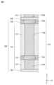
- the first electronic component layer 110 has one or more first electronic components 111 and a first electronic component layer through via 116, and further includes a first Si base layer 112, a first side wall portion 113, and a first resin sealing layer. It has a stop portion 114, a first electronic component adhesive layer 115, and a first Si through via 117.
- One or more first electronic components 111 are arranged within the first composite component layer 100.
- One or more first electronic components 111 have a first surface 111a perpendicular to the thickness direction and a second surface 111b opposite to the first surface 111a (first surface 111a and second surface 111b facing each other). It has a component body portion 111c, a plurality of first component electrodes 111d arranged on the first surface 111a, and a first insulating portion 111e arranged between the plurality of first component electrodes 111d.
- the first electronic component 111 is supported by the first Si base layer 112 via the first electronic component adhesive layer 115.
- the first electronic component 111 is sealed within the first composite component layer 100 by a first resin sealing portion 114 .
- the first component electrode 111d of the first electronic component 111 is electrically connected to the first rewiring layer 120 via the first Si through via 117.
- the first electronic components 111 may be of the same type or different types.
- the thickness of the first electronic component 111 is, for example, 80 to 120 ⁇ m.
- One or more first electronic components 111 are arranged such that the first surface 111a thereof is located on the first redistribution layer 120 side with respect to the second surface 111b. , disposed within the first composite component layer 100.
- the one or more second and third electronic components 211 and 311 are also all on the first surface thereof.
- 211a and 311a are arranged in the second and third composite component layers 200 and 300 so that they are located on the second and third redistribution layers 220 and 320 side with respect to the second surfaces 211b and 311b.
- These one or more electronic components 111, 211, and 311 are connected to rewiring layers 120, 220, and 320, respectively. In this way, since the composite component device 1 has simple wiring, not only two composite component layers but three or more composite component layers can be stacked.
- the one or more first electronic components 111 are, for example, electronic components in which one or more elements are integrated in a material similar to the material constituting the first Si base layer 112.
- the first electronic component 111 is, for example, an active component (more specifically, a CPU, a GPU, an LSI, etc.) and a passive component (more specifically, a capacitor, a resistor, an inductor, etc.).
- the first electronic component main body 111c includes, for example, ceramic or semiconductor material (more specifically, silicon, etc.).
- the first component electrode 111d is made of, for example, Cu, Ni, Sn, Al, or an alloy containing these as a conductive material.
- the conductive material is preferably the same material as the first Si through-via 117.
- the thickness of the first component electrode 111d is, for example, 1 ⁇ m to 30 ⁇ m, preferably 5 ⁇ m or less.
- the first component electrode 111d can be made as thin as 1 to 5 ⁇ m.
- the thickness of the first component electrode 111d can be, for example, 1/4 to 1/6 times the thickness of the first electronic component main body 111c.
- the first insulating portion 111e functions as a layer that electrically insulates between the first component electrodes 111d.
- the thickness of the first insulating portion 111e is, for example, 1 to 30 ⁇ m, preferably 5 ⁇ m or less.
- the first component electrode 111d can be made as thin as 1 to 5 ⁇ m.
- the thickness of the first insulating section 111e can be, for example, 1/4 to 1/6 times the thickness of the first electronic component main body section 111c.
- the thickness of the first insulating portion 111e may be the same as that of the first component electrode 111d, and in this case, the lower surface of the first insulating portion 111e and the lower surface of the first component electrode 111d are flush with each other.
- the first Si base layer 112 has a first main surface 112a and a second main surface 112b facing each other.
- the first Si base layer 112 supports one or more first electronic components 111 via the first electronic component adhesive layer 115 on the second main surface 112b, and supports the first redistribution layer 120 on the first main surface 112a.
- the first Si base layer 112 is substantially made of Si.
- substantially composed of Si as used herein means that the target member contains Si in a proportion of 99% by mass or more.
- the thickness of the first Si base layer 112 is, for example, 150 ⁇ m or less, preferably 50 ⁇ m or less, and more preferably 30 ⁇ m or less.
- the reason why the thickness of the first Si base layer 112 can be made extremely thin is that in the method for manufacturing the composite component device 1 described later, the first Si support 140 is bonded to the first Si base layer 112 to reinforce the strength. This is because even if the first Si base layer 112 is ground and thinned, damage (cracks, etc.) to the first Si base layer 112 due to insufficient strength is less likely to occur (see FIGS. 4E and 4F). The reinforcement of strength provided by the first Si support 140 makes it possible to manufacture the composite component device 1.
- the via wiring electrically connecting from the first component electrode 111d of one or more electronic components 111 to the first redistribution layer 120 (that is, the first The length of the through via 117) can be shortened. Thereby, the parasitic impedance due to the via wiring can be reduced, and the electrical characteristics of electronic equipment using the composite component device 1 can be improved.
- the first side wall portion 113 is arranged on the second main surface 112b of the first Si base layer 112 so as to surround one or more first electronic components 111.
- the first side wall portions 113 are arranged at both ends of the first composite component layer 100 so as to entirely surround one or more electronic components 111 .
- a first electronic component layer through-via 116 passes through the first side wall portion 113 .
- the first side wall portion 113 has a substantially rectangular shape in cross-sectional view, and is connected to the second redistribution layer 220 of the second composite component layer 200 via the first interlayer adhesive layer 130 on its upper surface, and is connected to the second redistribution layer 220 of the second composite component layer 200 on its lower surface. It is bonded to the first Si base layer 112 via the first electronic component adhesive layer 115.
- the thickness of the first side wall portion 113 is, for example, 90 to 130 ⁇ m.
- the first side wall portion 113 is, for example, substantially made of Si.
- the first resin sealing section 114 seals one or more first electronic components 111 .
- the resin sealing part 114 includes resin (for example, epoxy resin), and can integrate the plurality of (two or more) first electronic components 111 with the resin. Since the plurality of first electronic components 111 can be integrated with the resin, even if the two or more first electronic components 111 have different dimensions and shapes, the two or more first electronic components 111 can be integrated into the resin. 1 electronic component layer 110 . This allows design with a high degree of freedom, and allows two or more first electronic components 111 to be combined depending on the application. For example, the composite component device 1 can incorporate different types of first electronic components 111.
- the first electronic component adhesive layer 115 adheres one or more first electronic components 111 to the second main surface 112b of the first Si base layer 112.
- the thickness of the first electronic component adhesive layer 115 refers to the thickness in the Z direction from the lower surface of the first component electrode 111d to the second main surface 112b of the first Si base layer 112.
- the thickness of the first electronic component adhesive layer 115 is, for example, 4 to 6 ⁇ m.
- the electronic component layer in the composite component layer adjacent to the rewiring layer of another composite component layer among the two or more composite component layers has an electronic component layer through-via that electrically connects to the rewiring layer of the other composite component layer. It further has. That is, when the composite component layer is bonded to the rewiring layer of another composite component layer, it further includes an electronic component layer through-via electrically connected to the rewiring layer of the another composite component layer.
- the first electronic component layer 110 in the first composite component layer 100 adjacent to the second redistribution layer 220 of the second composite component layer 200 is electrically connected to the second redistribution layer 220 of the second composite component layer 200. It further includes a first electronic component layer through via 116 for connection.
- the first electronic component layer 110 since the first composite component layer 100 is connected to the second rewiring layer 220 of another second composite component layer 200, the first electronic component layer 110 is connected to the second rewiring layer 220 of the second composite component layer 200. It further includes a first electronic component through-layer via 116 electrically connected to layer 220.
- the second composite component layer 200 is connected to the third redistribution layer 320 of the third composite component layer 300
- the second electronic component layer 210 is electrically connected to the third redistribution layer 320 of the third composite component layer 300. It further includes a second electronic component layer through via 216 that is connected to the second electronic component layer.
- the third composite component layer 300 is not connected to the rewiring layer of another composite component layer, the third composite component layer 300 does not have an electronic component layer through-via.
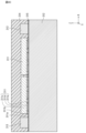
- the first electronic component layer through via 116 penetrates the first electronic component layer 110 in the Z direction (more specifically, the first electronic component layer 113, the first electronic component adhesive layer 115, and the first Si base layer 112 in the Z direction). ), and also penetrates the first interlayer adhesive layer 130 .
- the first electronic component layer through-via 116 includes an adhesive layer conductive via 116 a that penetrates the first interlayer adhesive layer 130 , a side wall through-via 116 b that penetrates the first side wall 113 , and a first electronic component layer that penetrates the first electronic component adhesive layer 115 .
- a conductive via 116c that penetrates through the first Si base layer 112, and a through-Si via 116d that penetrates the first Si base layer 112.
- the adhesive layer conductive via 116a electrically connects the first electronic component layer through-via 116 and the second redistribution layer 220 of the second composite component layer 200.
- the cross-sectional area of the adhesive layer conductive via 116a (cross-sectional area in the XY plane) is larger than the cross-sectional area of the side wall through-via 116b. Therefore, the electrical connection between the first electronic component layer through-via 116 and the second redistribution layer 220 is improved, and the connection resistance between the first and second composite component layers 100 and 200 is reduced, which improves reliability. further improves.
- the first electronic component layer through-via 116 preferably consists essentially of copper.
- substantially made of copper (Cu) means that the target member contains copper in a proportion of 99% by mass or more.
- the first Si through via 117 penetrates the first Si base layer 112 (and the first electronic component adhesive layer 115) and connects the first component electrode 111d and the first redistribution layer 120. Connect electrically.
- the first Si through via 117 has a Si through via main body portion 117a and an extension portion 117b.
- the Si through-via main body portion 117a is electrically connected to the first redistribution layer 120 and penetrates through the first Si base layer 112.
- the extending portion 117b is electrically connected to the Si through-via main body portion 117a, extends from the second main surface 112b of the first Si base layer 112, penetrates the inside of the first electronic component adhesive layer 115, and connects to the first component electrode. It is electrically connected to 111d.
- the via wiring that electrically connects the first component electrode 111d to the first redistribution layer 120 is configured only from the first Si through-via 117, and therefore does not have (does not require) bumps (for example, solder bumps). ). Therefore, the composite component device 1 according to this embodiment can further reduce parasitic impedance due to via wiring. Furthermore, this improves the electronic characteristics of electronic equipment that uses the composite component device 1.
- the length of the via wiring (that is, the length of the first Si through-via 117 in the stacking direction) is, for example, 3 ⁇ m to 36 ⁇ m.
- solder bumps typically have a diameter of 100-150 ⁇ m.
- the first Si through-via 117 is approximately linear in the stacking direction.
- the cross-sectional shape of the first Si through-via 117 in the ZX plane is approximately rectangular in FIG. 2 .
- the cross-sectional shape of the first Si through-via 117 in the XY plane is, for example, a substantially circular shape, a substantially polygonal shape, or a substantially polygonal shape with rounded corners.
- the first redistribution layer 120 is formed on the first main surface 112a of the first Si base layer 112.
- the first rewiring layer 120 is a multilayer wiring layer.
- the first redistribution layer 120 includes a wiring (conductive wiring) 120b and a dielectric film 120a substantially made of an inorganic material (inorganic insulating material).
- the wiring 120b has a conductive via.
- the conductive via electrically connects wiring between different layers within the first redistribution layer 120.
- Wiring 120b includes a conductive material.
- the conductive material is, for example, Cu, Ag, and Au, and alloys containing them, and among these, Cu is preferred.
- the first redistribution layer 120 can have a plurality of layers, and includes, for example, two or more layers of wiring 120b and one or more layers of dielectric film 120a.
- the thickness of one layer of wiring 120b and one layer of dielectric film 120a constituting the first redistribution layer 120 is, for example, 1.5 ⁇ m to 5.0 ⁇ m.
- the thickness of the first redistribution layer 120 is the value obtained by multiplying the thickness of one of these layers (1.5 ⁇ m to 5.0 ⁇ m) by the total number of layers in the first redistribution layer 120 (unit: ⁇ m) becomes.
- the dielectric film 120a is substantially made of an inorganic material (inorganic insulating material) as an insulating material.
- substantially composed of an inorganic material means that the target member contains an inorganic material in a proportion of 99% by mass or more.
- inorganic insulating materials include silicon oxide (SiO 2 ) and silicon nitride (SiN, Si 3 N 4 ). If the dielectric film 120a is made of an inorganic insulating material, the wiring width can be reduced to about 1/10 of that of the dielectric film in the composite component device 1A according to the second embodiment, for example. This makes it possible to further reduce the size and height of the composite component device 1.
- the line and space (L/S) of the first redistribution layer 120 including the dielectric film 120a substantially made of an inorganic material is, for example, 1 ⁇ m/1 ⁇ m.
- the thickness of the dielectric film 120a is, for example, 0.1 to 2 ⁇ m.
- the dielectric film 120a may be a multi-component film containing two or more types of components.
- the multicomponent film may be a multilayer film in which a plurality of layers are formed for each component.
- the layer structure of the multilayer film is, in order from the first Si base layer 112 side, SiO 2 (thickness 0.25 ⁇ m)/Si 3 N 4 (thickness 0.1 ⁇ m)/SiO 2 (thickness 0.25 ⁇ m)/Si 3 N. 4 (thickness 0.1 ⁇ m).
- the first interlayer adhesive layer 130 adheres the first electronic component layer 110 and the second redistribution layer 220 of the second composite component layer 200 .
- the method for manufacturing the composite component device 1 according to the first embodiment includes, for example, An electronic method for bonding one or more electronic components to a Si base layer such that a plurality of component electrodes of the one or more electronic components are in contact with the bottom surface of the Si base layer having a lattice-shaped sidewall via an electronic component adhesive layer.
- an electronic component sealing step of sealing one or more electronic components with resin to form a resin sealing part a rewiring layer forming step of forming a rewiring layer to create a composite component layer
- Another composite component layer is formed by an electronic component adhesion process, an electronic component sealing process, and a rewiring layer forming process, and an electronic component layer through-via is formed on the side wall of the other composite component layer to add another composite component layer to the composite component layer.
- a lamination process of laminating composite component layers is performed at least once.
- the method for manufacturing the composite component device 1 according to the first embodiment is as follows: a Si base layer thinning step for thinning the Si base layer; A through hole forming step of forming a through hole in the thinned Si base layer and the electronic component adhesive layer to expose a part of the surface of the component electrode; The method further includes a through-Si via forming step of forming a through-Si via in the through-hole.
- the method for manufacturing the composite component device 1 according to the first embodiment further includes: a Si base layer preparation step for preparing a Si base layer; an insulating part forming step of forming an insulating part between component electrodes; a resin sealing part thinning process for thinning the resin sealing part; a Si support bonding step of bonding a Si support to an electronic component layer; a dielectric film forming step of forming a dielectric film having a predetermined pattern on the Si base layer;
- the method may also include a dicing step of dividing the method into individual pieces by dicing.
- FIGS. 10A to 10B and FIGS. 4A to 4V are diagrams for explaining a method for manufacturing the composite component device 1.
- FIG. The manufacturing method of the composite component device 1 according to the first embodiment includes an insulating part forming process, a Si base layer preparation process, an electronic component bonding process, an electronic component sealing process, a resin sealing part thinning process, Includes a Si support bonding process, a Si base layer thinning process, a dielectric film formation process, a through hole formation process, a Si through via formation process, a rewiring layer formation process, a lamination process, and a dicing process.
- a mother assembly in which composite component devices 1 are integrated is produced from the electronic component bonding process to the lamination process. Further, in this manufacturing method, the third composite component layer 300, the second composite component layer 200, and the first composite component layer 100 are manufactured in this order.
- a first insulating part 111e is formed between the first component electrodes 111d of the first electronic component 111.
- a coating film containing resin is formed, and a planarization process is performed to form the first insulating portion 111e.
- a solution containing a resin and a solvent is applied using a spin coating method to form a coating film.
- the lowest part of the coating film is made higher than the highest part of the first component electrode 111d. That is, the coating film is formed so that all of the plurality of first component electrodes 111d are completely buried in the coating film.
- the coating layer is dried to form the first insulating portion 111e.
- the first insulating portion 111e before the subsequent planarization process preferably completely covers the first component electrode 111d.
- the surfaces of the first component electrode 111d and the first insulating section 111e are ground and planarized using, for example, a surface planer and a grinder, and a first component electrode is formed between the first component electrodes 111d. 1 insulating section 111e is formed. As a result, the top surface of the first component electrode 111d is exposed, and the top surfaces of the first component electrode 111d and the first insulating section 111e are flush with each other.
- a third Si base layer 312 is prepared. Specifically, in the Si base layer preparation step, as shown in FIG. 4A, a Si wafer is prepared as the third Si base layer 312, and a third electronic component adhesive layer 315 (strictly speaking, An adhesive coating film) is formed, and the third side wall portion 313 is arranged. As a result, the third Si base layer 312 is formed, which has a rectangular bottom portion in plan view and sidewall portions arranged in a grid so as to surround the rectangular bottom portion.
- One or more third electronic components 311 are bonded to the recess (or depression, or cavity) surrounded by the bottom and side walls in an electronic component bonding process described later.
- the adhesive coating film is formed on the second main surface 312b of the third Si base layer 312. In this way, the third Si base layer 312 on which the coating film is formed is produced.
- the coating method is, for example, spin coating.
- the thickness of the coating film is controlled to be within the range of 10 ⁇ m from the thickness of the third component electrode 311d of the third electronic component 311 of one or more.
- the adhesive is, for example, a thermosetting resin.
- a thermosetting resin is, for example, a thermosetting resin containing a repeating unit derived from benzocyclobutene (BCB), and for example, 1,3-divinyl-1,1,3,3-tetramethyldisiloxane-bis. -Can be obtained by polymerizing benzocyclobutene (DVS-bis-BCB).
- a commercially available product is, for example, "CYCLOTENE" manufactured by Dow Chemical.
- the shape of the Si wafer may be a flat cylindrical shape when viewed from above, but is not limited to this.
- flatness means that the height (h) of the cylindrical shape is smaller than the outer diameter (diameter: 2r) (h/2r ⁇ 1).
- the thickness of the Si wafer is, for example, 775 ⁇ m (Si wafer diameter ⁇ 300 mm), 725 ⁇ m ( ⁇ 200 mm), 675 ⁇ m ( ⁇ 150 mm), and 525 ⁇ m ( ⁇ 100 mm).
- the Si base layer preparation step may be performed before the insulating portion forming step.
- Both the third Si base layer 312 and the third side wall portion 313 are substantially made of Si.
- a plurality of third component electrodes 311d of one or more third electronic components 311 are bonded to a third electronic component adhesive layer 315 on the bottom surface of the third Si base layer 312 having the third side wall portion 313 in a lattice shape.
- One or more third electronic components 311 are bonded to the third Si base layer 312 so as to be in contact therewith.
- the third component electrode 311d and the third insulating portion 311e are bonded to each other through the third electronic component adhesive layer 315 (strictly speaking, an adhesive coating film).
- one or more third electronic components 311 are arranged (mounted) on (the bottom surface of) the third Si base layer 312 so as to be in contact with (the bottom surface of) the third Si base layer 312 .
- the adhesive coating is cured to form a third electronic component adhesive layer 315.
- one or more third electronic components 311 are bonded onto the third Si base layer 312.
- the third electronic component 311 is placed on the coating film using a device equipped with a vacuum chamber. Specifically, an electronic component integrated wafer (a wafer in which one or more third electronic components 311 are integrated) is bonded to the third Si base layer 312 (the third Si base layer 312 having the third side wall portion 313). Pressure is applied in both directions along the stacking direction of the third electronic component 311 to heat it. Specifically, the third Si base layer 312 is set on the lower stage in the vacuum chamber of the apparatus. The third electronic component 311 is vacuum-suctioned (or vacuum-suctioned) to the upper stage in the vacuum chamber so that the third component electrode 311d of the third electronic component 311 faces the coating film.
- a recognition mark on the third Si base layer 312 is used to align the third Si base layer 312 with the electronic component integrated wafer.
- One or more third electronic components 311 are arranged on the coating film side of the third Si base layer 312. Pressure is applied in both directions along the direction in which the upper and lower stages face each other to heat the stage.
- the electronic component integrated wafer is bonded onto the third Si base layer 312 such that the third component electrode 311d and the third insulating portion 311e face the third Si base layer 312 via the third electronic component adhesive layer 315. .
- one or more third electronic components 311 are sealed with resin to form a third resin sealing portion 314 .
- a liquid resin is applied using a dispenser onto the third Si base layer 312 on which one or more third electronic components 311 are mounted. Thereafter, the applied liquid resin is molded using a compression molding device. The liquid resin is then cured using, for example, a hot air circulation oven. The heat treatment conditions for curing are, for example, 150° C. for 1 hour. As a result, a third resin sealing portion 314 is formed.
- the third resin sealing part 314 is thinned. Specifically, in the resin sealing part thinning step, as shown in FIG. 4D, the third resin sealing part 314 is ground and thinned using a Si wafer back grinder. In the electronic component thinning step, the surface of the third resin sealing portion 314 on the second surface 311b side of the third electronic component 311 is ground. It is preferable that the amount of grinding is as large as possible.
- the thickness of the third resin sealing portion 314 after thinning is, for example, 50 to 150 ⁇ m.
- the third resin sealing part 314 of the third electronic component layer 310 is ground, but it is also possible to grind one or more third electronic components 311. good. However, care should be taken not to damage the internal functional parts of the third electronic component 311.
- the functional parts are, for example, a dielectric and an electrode in the case of a capacitor, and wiring in the case of an inductor.
- a third Si support 340 is bonded to the third resin sealing portion 314.
- the Si wafer described in the Si base layer preparation step is separately prepared as the third Si support 340.
- an adhesive layer 350 (strictly speaking, an adhesive coating film) is formed on the third Si support 340 by the method described in the electronic component bonding process.
- the third resin sealing part 314 is bonded onto the third Si support 340 so that the ground surface of the third resin sealing part 314 comes into contact with the coating film, and heating is performed by applying pressure.
- the adhesive coating film is cured to form an adhesive layer 350, and the third Si support 340 is placed on the ground surface of the third resin sealing part 314 via the adhesive layer 350.
- the purpose of providing the third Si support 340 is to prevent the occurrence of adverse effects (more specifically, a decrease in strength, etc.) due to the thinner layer in the manufacturing process than in the past in the subsequent Si base layer thinning process. be.
- the third Si support 340 can be thinned before bonding, if necessary, from the viewpoint of improving processability. This is because a dielectric film will be formed using a semiconductor device in a subsequent process. For example, if the thickness of the third electronic component 311 is 150 ⁇ m, the Si wafer ( ⁇ 300 mm, typical thickness 775 ⁇ m) serving as the third Si support 340 is thinned to about 625 ⁇ m.
- the third Si base layer 312 is thinned. Specifically, in the Si base layer thinning process, as shown in FIG. 4F, the third Si base layer 312 is ground and thinned using the same method as the resin sealing part thinning process. to flatten the ground surface. In the Si base layer thinning process, since the third Si base layer 312 is thinned while being supported by the third Si support 340, the third Si base layer 312 can be effectively thinned. As a result, the method for manufacturing a composite component device 1 according to the present embodiment can manufacture a composite component device 1 that is an excellent electronic component module and has a reduced height and size.
- the amount of grinding is preferably as large as possible within a range that prevents the above disadvantages and maintains a certain strength, for example.
- the thickness of the third Si base layer 312 after thinning is preferably 3 ⁇ m or more.
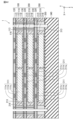
- FIGS. 4G to 4I are enlarged views of a portion corresponding to section C in FIG. 4F.
- FIGS. 4J to 4M are diagrams mainly related to the formation of the third Si through via 317 and the third redistribution layer 320, for convenience, the third Si through via 317, the third redistribution layer 320, and the like are not formed. Please note that the area has expanded to occupy a large portion of the area.
- a chemical vapor deposition (CVD) method such as plasma-enhanced chemical vapor deposition (PECVD) is used to deposit the entire surface of the third Si base layer 312, as shown in FIG. 4G.
- a dielectric film (thickness: 0.1 to 0.2 ⁇ m) 320a is formed thereon.
- the dielectric film 320a may have one or more layers.
- SiO 2 : 0.25 ⁇ m/Si 3 N 4 0.1 ⁇ m/SiO 2 : 0.25 ⁇ m/Si 3 N 4 0 .1 ⁇ m.
- the surface of the third Si base layer 312 can be cleaned before forming the dielectric film 320a. Cleaning is, for example, wet cleaning and oxygen plasma ashing.
- the dielectric film 320a is patterned using a photolithography method.
- a photoresist film 360 is formed on the entire surface of the dielectric film 320a by spin coating a liquid resist.
- the photoresist film 360 is exposed to light through a mask corresponding to a predetermined pattern.
- the exposed photoresist film 360 is developed.
- the dielectric film 320a of the photoresist film 360 is selectively removed using RIE (Reactive Ion Etching). For example, when the above-mentioned four-layer dielectric film 320a is formed, two layers on the surface side of the dielectric film 320a (the surface side of the dielectric film 320a facing the third Si base layer 312 side) are selectively removed.
- RIE Reactive Ion Etching
- the photoresist film 360 is peeled off.
- a dielectric film 320a having a predetermined pattern is formed on the third Si base layer 312.
- the dielectric film 320a also functions as an insulating film that electrically insulates between two third Si through vias 317 shown in FIG. 4L, which will be described later.
- the first main surface 312a of the third Si base layer 312 may further include a mark layer.
- the mark layer can be detected with an infrared (IR) camera for alignment in photolithographic methods.
- through holes 312c and 315c are formed in the thinned third Si base layer 312 and third electronic component adhesive layer 315 to expose a part of the surface of the third component electrode 311d.
- a photoresist film 360 is formed over the entire surface.
- the photoresist film 360 is exposed through a mask corresponding to the pattern of the third Si through-via 317.
- the exposed photoresist film 360 is developed to form a photoresist film 360 having a predetermined pattern as shown in FIG. 4J. As shown in FIG.
- the third Si base layer 312 and the third electronic component adhesive layer 315 that are present in the Z direction from the opening 360a of the photoresist film 360 are selectively removed (etched). Etching is performed using, for example, RIE and laser irradiation. As a result, through holes 312c and 315c are formed, and the third component electrode 311d (part of the upper surface) is exposed.
- the through hole 315c of the third electronic component adhesive layer 315 in the ZX cross section has a substantially elliptical shape.
- the term "approximately elliptical shape” includes not only a strict elliptical shape but also a similar elliptical shape that takes into account actual variations in etching conditions during manufacturing.
- the material forming the third electronic component adhesive layer 315 is more easily etched than the material forming the third Si base layer 312. As a result, a substantially elliptical extending portion 317b is formed in the subsequent Si through-via forming step.
- the photoresist film 360 is removed.
- the etching means is preferably RIE. By using RIE as the etching means, the flatness of the exposed upper surface of the third component electrode 311d is improved, so that a good bond can be formed with the third Si through via 317 that will be formed later. Thereby, deterioration in electrical connectivity can be further suppressed.
- Si through-via formation process In the Si through-via forming step, a Si through-via is formed in the through hole. Specifically, in the through hole forming step, as shown in FIG. 4L, third Si through vias 317 are formed in the through holes 312c and 315c by electroplating. A third Si through via 317 is formed in the through holes 312c and 315c by electrolytic plating (more specifically, electrolytic Cu plating) using a dual damascene method (more specifically, a Cu dual damascene method). As a result, the third electronic component layer 310 is formed.
- a third rewiring layer 320 is formed to produce the third composite component layer 300.
- a dielectric film 320a and wiring 320b having a predetermined pattern are formed by the above-described photolithography method and etching, and the third rewiring layer 320 form.
- FIG. 4M shows a cross-sectional view of the third composite component layer 300 that includes FIG. 4M.
- FIG. 4M is an enlarged view of section C' in FIG. 4N.
- the lamination process In the lamination process, another composite component layer (first and second composite component layers 100, 200) is formed by the above-mentioned insulation part formation process to rewiring layer formation process, and an electronic component layer penetrating layer is formed in the other composite component layer. Vias 116 and 216 are formed to laminate the third composite component layer 300 with the other composite component layer. In this embodiment, the composite component layer is laminated twice. Specifically, first, in the lamination step, the second composite component layer 200 is laminated on the third composite component layer 300. The second composite component layer 200 is formed by the steps of forming an insulating part and forming a rewiring layer shown in FIGS. 4A to 4M.
- the second Si support 240 is removed from the second composite component layer 200 to which the second Si support 240 is bonded, and a second Si support is newly added to the second redistribution layer 220 of the second composite component layer 200, as shown in FIG. 4O.
- 240 is laminated.
- the second composite component layer 200 shown in FIG. 4O is bonded to the third composite component layer 300 shown in FIG. 4N using the second interlayer adhesive layer 230.
- the second Si support 240 is removed as shown in FIG. 4Q.
- a second electronic component layer through-via 216 is formed in the second composite component layer 200.
- the second electronic component layer through-via 216 can be formed by the same means as the Si through-via process described above.
- the second composite component layer 200 is laminated onto the third composite component layer 300.
- first composite component layer 100 is laminated.
- first composite component layer 100 is laminated on the second composite component layer 200 as shown in FIGS. 4A to 4P (see FIG. 4S).
- the first Si support 140 is removed as shown in FIG. 4T.
- first electronic component layer through-vias 116 are formed in the first composite component layer 100.
- the first electronic component layer through-via 116 can be formed by the same means as the Si through-via process described above.
- the first composite component layer 100 is further laminated.
- the composite component device according to the second embodiment has Si base layers 112, 212, 312, side wall portions 113, 213, 313, and Si through vias 117, 217, 317, compared to the composite component device according to the first embodiment. They are different in that they do not have a metal layer 370, and that electronic component adhesive layers 115, 215, 315 and electronic component layer through-vias 116, 216, 316 are different. This different configuration will be mainly explained below. Note that in the second embodiment, the same reference numerals as those in the first embodiment have the same configuration as those in the first embodiment, so the description thereof will be omitted in principle.
- FIG. 5 is a diagram schematically showing a cross section of a composite component device according to a second embodiment of the present disclosure. Similar to the first embodiment, the configurations of the second and third composite component layers 200 and 300 are almost the same as the first composite component layer 100, so the first composite component layer 100 will be mainly described below. However, matters that are different from the first composite component layer 100 may be referred to in the second and third composite component layers 200 and 300.
- the first electronic component layer 110 includes a first electronic component 111 and a first electronic component layer through-via 116A, and further includes a first resin sealing portion 114 and a first electronic component adhesive layer 115A.
- the first electronic component 111 is supported by the first redistribution layer 120A.
- the first component electrode 111d of the first electronic component 111 is directly electrically connected to (directly joined to) the first rewiring layer 120.
- the first electronic component adhesive layer 115A adheres the second surface 111b of the first electronic component 111 to the second redistribution layer 220A of the second composite component layer 200.
- the second electronic component adhesive layer 215A adheres the second surface 211b of the second electronic component 211 to the third rewiring layer 320 of the third composite component layer 300.
- the third electronic component adhesive layer 315A adheres the second surface 311b of the third electronic component 311 to the metal layer 370.
- the first electronic component layer through-via 116A is a columnar wiring (more specifically, a Cu pillar).
- the cross-sectional area of the first electronic component layer through via 116A in the XY plane is larger than that of the first electronic component layer through via 116 in the first embodiment.
- the cross-sectional diameter of the first electronic component layer through-via 116A in the XY plane is, for example, 35 to 100 ⁇ m.
- the number of first electronic component layer through-vias 116A is four in total in cross-sectional view, and two are arranged at each end of the first composite component layer 100.
- the cross-sectional area of the first electronic component layer through-via 116A in a plane perpendicular to the thickness direction of the composite component device 1A may increase from the second surface 111b of the first electronic component 111 toward the first surface 111a. That is, the shape of the first electronic component layer through-via 116A in the ZX cross section (ZX cross section shape) may be tapered with respect to the stacking direction of the composite component layers 100, 200, and 300. More specifically, the cross-sectional area (XY cross-sectional area) of the first electronic component layer through-via 116A in the XY plane may decrease from the second surface 111b toward the first surface 111a.
- the first rewiring layer 120A is directly connected to the first component electrode 111d. If the first redistribution layer 120A is directly connected to the first component electrode 111d, the length of the via wiring between the first redistribution layer 120A and the first component electrode 111d can be further reduced. Devices can be made smaller and lower in height, and the electrical resistance of via wiring can also be lowered.
- the first redistribution layer 120A includes a dielectric film substantially made of an organic material (organic insulating material) and wiring (conductive wiring).
- the expression that the dielectric film is substantially composed of an organic material means that the dielectric film contains an organic material in a proportion of 99% by mass or more.
- the dielectric film essentially consists of an organic insulating material as an insulating material. Examples of organic insulating materials include epoxy resin, silicone resin, polyester, polypropylene, polyimide, acrylonitrile-butadiene-styrene (ABS) resin, acrylonitrile-styrene (AS) resin, methacrylic resin, polyamide, fluororesin, liquid crystal polymer, and polyamide.
- the dielectric film is formed without using a method such as PECVD, so the cost is lower than that of the composite component device 1 according to the first embodiment. can be reduced.
- the line and space (L/S) of the first redistribution layer 120A including a dielectric film substantially made of an inorganic material is, for example, 10 ⁇ m/10 ⁇ m.
- the thickness of the dielectric film is, for example, 1 to 20 ⁇ m.
- the third composite component layer 300 has a metal layer 370.
- Metal layer 370 functions as an electromagnetic shield for composite component device 1A.
- the method for manufacturing the composite component device 1A according to the second embodiment includes, for example, an electronic component bonding step of bonding one or more electronic components to the Si support so that the second surface of the one or more electronic components contacts the Si support (Si support base material) via an electronic component adhesive layer; an electronic component sealing step of sealing one or more electronic components with resin to form a resin sealing part; a resin sealing part thinning step of thinning the resin sealing part to expose the entire surface of the component electrode; a rewiring layer forming step of forming a rewiring layer to create a composite component layer; An electronic component layer through via is formed on the composite component layer, and one or more electronic components are attached to the composite component layer such that the second surface of the one or more electronic components contacts the composite component layer via the electronic component adhesive layer.
- One or more electronic components are bonded and sealed with resin to form a resin sealing part, the resin sealing part is thinned to expose the entire surface of the component electrode, and a rewiring layer is formed to form a composite component layer. and a lamination step of laminating another composite component layer on the The lamination step is performed at least once.
- the method for manufacturing the composite component device 1A according to the second embodiment further includes: an insulating part forming step of forming an insulating part;
- the method may also include a dicing step of dividing the method into individual pieces by dicing.
- FIGS. 6A to 6O are diagrams for explaining a method of manufacturing the composite component device 1A.
- the manufacturing method of the composite component device 1A according to the second embodiment includes, in chronological order, an insulating part forming process, an electronic component bonding process, an electronic component sealing process, a resin sealing part thinning process, and a rewiring process. It includes a layer forming process, a laminating process, and a dicing process.
- the insulating part forming step see FIGS. 10A and 10B
- the electronic component sealing step see FIG. 6B
- the dicing step see FIG. 6O
- one or more third Si supports 340 are bonded to one or more third Si supports 340 such that the second surfaces 311b of one or more third electronic components 311 are in contact with the third Si supports 340 via the third electronic component adhesive layer 315A.
- the electronic component 311 is bonded. Specifically, in the electronic component bonding process, as shown in FIG.
- the second surface of the third electronic component 311 (the third insulating part 311e was formed in the same manner as the insulating part forming process of the first embodiment)
- a third electronic component adhesive layer 315A (strictly speaking, an adhesive coating film) is formed on the third electronic component adhesive layer 315A (strictly speaking, an adhesive coating film), and a third Si support 340 (strictly speaking, a metal layer 370 is arranged through the adhesive layer 350).
- One or more third electronic components 311 are arranged (mounted) on the third Si support 340).
- the third electronic component adhesive layer 315A is cured. As a result, one or more third electronic components 311 are bonded onto the third Si support 340.
- the third resin sealing part 314 is thinned to expose the entire surface of the third component electrode 311d.
- the third resin sealing part 314 is ground and thinned using a Si wafer back grinder. This exposes the entire surface of the third component electrode 311d. Note that in this step, part of the component electrode 311d and the third insulating part 311e may be ground.
- the third composite component layer 300 is produced by forming the third rewiring layer 320A. Specifically, in the rewiring layer forming step, as shown in FIG. 6D, a dielectric film and wiring having a predetermined pattern are formed using a photolithography method to form the third rewiring layer 320A. In the second embodiment, since a relatively expensive device such as PVCVD is not used to form the dielectric film, costs can be reduced.
- the second electronic component layer through-via 216A is formed on the third composite component layer 300, and the second surface 211b of one or more second electronic components 211 is bonded to the second electronic component layer 300.
- One or more second electronic components 211 are adhered to the third composite component layer 300 so as to be in contact with each other through the layer 215A, and the one or more second electronic components 211 are sealed with resin to form a second resin sealing part.
- the second resin sealing part 214 is thinned to expose the entire surface of the second component electrode 311d, and a second rewiring layer 220A is formed to add another composite component layer to the third composite component layer 300. (first and second composite component layers 100, 200) are laminated.
- the lamination process is performed twice.
- the second composite component layer 200 is laminated on the third composite component layer 300.
- a second electronic component layer through-via 216A is formed on the third composite component layer 300.
- a dry film resist (DFR) is laminated on (the entire surface of) the third redistribution layer 320A of the third composite component layer 300.
- An opening is formed through the DFR by photolithography.
- a second electronic component layer through-via 216A is formed in the opening by Cu via plating. Peel off the DER.
- the second electronic component layer penetrating via 216A is formed on the third composite component layer 300.
- the second surface 211b of one or more second electronic components 211 is brought into contact with the third composite component layer 300 via the second electronic component adhesive layer 215A. Then, one or more second electronic components 211 are bonded to the third composite component layer 300.
- one or more second electronic components 211 are sealed with resin to form a second resin sealing portion 214.
- the second resin sealing part 214 is thinned to expose the entire surface of the second component electrode 211d and the second insulating part 211e, as shown in FIG. 6H.
- a second rewiring layer 220A is formed as shown in FIG. 6I.
- the second composite component layer 200 is laminated on the third composite component layer 300.
- the first composite component layer 100 is laminated on the second composite component layer 200. Similar to the formation of the second composite component layer 200 in the above-described lamination process, the first composite component layer 100 is laminated on the second composite component layer 200, as shown in FIGS. 6J to 6N.
- a composite component device 1A according to the second embodiment is manufactured through the dicing process shown in FIG. 6O.
- the composite component device according to the third embodiment has Si base layers 112, 212, 312, electronic component adhesive layers 115, 215, 315, and Si through vias 117, 217, 317, compared to the composite component device according to the first embodiment.
- the difference is that the electronic component layer through-vias 116, 216, and 316 are different.
- This different configuration will be mainly explained below. Note that in the third embodiment, the same reference numerals as those in the first and second embodiments have the same configurations as in the first and second embodiments, so the description thereof will be omitted in principle.
- FIG. 7 is a diagram schematically showing a cross section of a composite component device according to a third embodiment of the present disclosure.
- FIG. 8 is an enlarged view of section D in FIG. 7.
- the first composite component layer 100 includes a first electronic component layer 110 and a rewiring layer 120A provided in the first electronic component layer 110.
- the first electronic component layer 110 includes a first electronic component 111 and a first electronic component layer through-via 116B, and further includes a first side wall portion 113 and a first resin sealing portion 114.
- the first electronic component layer through-via 116B penetrates the first side wall portion 113 of the first electronic component layer 110 in the Z direction, and also penetrates the first interlayer adhesive layer 130.
- the first electronic component layer through-via 116B includes an adhesive layer conductive via 116a that penetrates the first interlayer adhesive layer 130 and a sidewall through-via 116b that penetrates the first sidewall 113.
- the method for manufacturing the composite component device 1B according to the third embodiment includes, for example, An electronic method for bonding one or more electronic components to a Si base layer such that a plurality of component electrodes of the one or more electronic components are in contact with the bottom surface of the Si base layer having a lattice-shaped sidewall via an electronic component adhesive layer.
- a lamination process of laminating composite component layers; It consists of A lamination step is performed at least once.
- the manufacturing method of the composite component device 1B according to the third embodiment is as follows: The method further includes a Si base layer removal step of removing the Si base layer and the electronic component adhesive layer to expose the entire surface of the component electrode.
- the method for manufacturing the composite component device 1B according to the third embodiment further includes: a Si base layer preparation step for preparing a Si base layer; an insulating part forming step of forming an insulating part; a resin sealing part thinning process for thinning the resin sealing part; a Si support bonding step of bonding a Si support to an electronic component layer;
- the method may also include a dicing step of dividing the method into individual pieces by dicing.
- FIGS. 9A to 9J are diagrams for explaining the manufacturing method of the composite component device 1B.
- the manufacturing method of the composite component device 1B according to the third embodiment includes an insulating part forming step, a Si base layer preparation step, an electronic component bonding step, an electronic component sealing step, a resin sealing portion thinning step,
- the process includes a Si support bonding process, a Si base layer removal process, a rewiring layer formation process, a lamination process, and a dicing process.
- the insulating part forming step to the Si support bonding step are performed (see FIGS. 4A to 4E).
- Si base layer removal process In the Si base layer removal step, the third Si base layer 312 and the third electronic component adhesive layer 315 are removed to expose the entire surface of the third component electrode 111d. Specifically, in the Si base layer removal process, as shown in FIG. 9A, the third Si base layer 312 and the third electronic component adhesive layer are removed using the same means as the Si base layer thinning process in the first embodiment. 315 is removed.
- a third rewiring layer 320A is formed. Specifically, in the rewiring layer forming step, the third rewiring layer 320A is formed as shown in FIG. 9B using the same means as the rewiring layer forming step in the second embodiment. As a result, the third composite component layer 300 is formed.
- the lamination process is similar to the lamination process of the first embodiment, in which another composite component layer (first, second Composite component layers 100, 200) are formed, electronic component layer through-vias 116B, 216B are formed in the other composite component layer, and the other composite component layer is laminated on the third composite component layer 300.
- another composite component layer first, second Composite component layers 100, 200
- electronic component layer through-vias 116B, 216B are formed in the other composite component layer
- the other composite component layer is laminated on the third composite component layer 300.
- the composite component devices 1, 1A, and 1B are provided with three composite component layers, but the present invention is not limited thereto.
- a composite component device may include two or more composite component layers.
- the lamination step is performed once or three or more times in the method for manufacturing a composite component device.
- the wiring design is less likely to be complicated, and the composite component layers can be electrically connected easily. Therefore, even if three or more composite component layers are laminated, wiring can be easily formed. Therefore, in circuit design, there are fewer restrictions on the number and types of built-in electronic components, and the degree of freedom in design is high. Various circuit configurations become possible, and the range of applications to which it can be applied becomes wider.
- the composite component device had two electronic components of the same type in each composite component layer, but the invention is not limited to this.
- a composite component device may have different types of electronic components, and may have one or more electronic components in each composite component layer.
- a composite component device may have a different number of electronic components in each composite component layer. Therefore, in circuit design, there are fewer restrictions on the number and types of built-in electronic components, and the degree of freedom in design is high. Various circuit configurations become possible, and the range of applications to which it can be applied becomes wider.
- a composite component device comprising two or more composite component layers having an electronic component layer and a rewiring layer provided on the electronic component layer, The two or more composite component layers are laminated in the thickness direction so that the electronic component layer and the rewiring layer are alternately arranged,
- the electronic component layer is
- the electronic component has one or more electronic components having a first surface perpendicular to the thickness direction and a second surface opposite to the first surface, and a plurality of component electrodes disposed on the first surface.
- the component electrodes of the one or more electronic components are electrically connected to the rewiring layer
- the electronic component layer in the composite component layer adjacent to the rewiring layer of another composite component layer among the two or more composite component layers is:
- the composite component device further comprises an electronic component layer through-via electrically connected to the redistribution layer of the another composite component layer.
- the electronic component layer further includes a resin sealing part that seals the one or more electronic components.
- All electronic components included in the composite component device are arranged within the two or more composite component layers such that the first surface thereof is located on the rewiring layer side with respect to the second surface, ⁇ 1 > to ⁇ 3>.
- ⁇ 5> The electronic component layer is The composite component device according to any one of ⁇ 1> to ⁇ 4>, further comprising a side wall portion arranged to surround the one or more electronic components and through which the electronic component layer through-via passes.
- the electronic component layer is a Si-based layer supporting the one or more electronic components;
- ⁇ 7> The composite component device according to any one of ⁇ 1> to ⁇ 6>, wherein the rewiring layer has a dielectric film substantially made of an inorganic material.
- the composite component layer is bonded to the other composite component layer via an adhesive layer
- the electronic component layer through-via has a sidewall through-via that penetrates the sidewall and a conductive via that penetrates the adhesive layer,
- the conductive via electrically connects the electronic component layer through-via and the rewiring layer of the another composite component layer
- the composite component device according to ⁇ 5> wherein a cross-sectional area of the conductive via is larger than a cross-sectional area of the side wall through-via in a plane perpendicular to the thickness direction.
- ⁇ 9> The composite component device according to any one of ⁇ 1> to ⁇ 4>, wherein the rewiring layer is directly connected to the component electrode.
- ⁇ 10> The composite component device according to any one of ⁇ 1> to ⁇ 5> and ⁇ 9>, wherein the rewiring layer has a dielectric film substantially made of an organic material.
- ⁇ 11> The composite component device according to ⁇ 10>, wherein a cross-sectional area of the electronic component layer through-via in a plane perpendicular to the thickness direction increases from the second surface toward the first surface.
- a method for manufacturing the composite component device comprising:
- the electronic component layer of the composite component device is a side wall portion arranged to surround the one or more electronic components and through which the electronic component layer through-via passes; further comprising a resin sealing part that integrates the one or more electronic components,
- the one or more electronic components are attached to the Si base layer so that the plurality of component electrodes of the one or more electronic components are in contact with the bottom surface of the Si base layer having a grid-like side wall portion via an electronic component adhesive layer.
- a Si base layer thinning step of thinning the Si base layer a through-hole forming step of forming a through-hole in the thinned Si base layer and the electronic component adhesive layer to expose a part of the surface of the component electrode; further comprising a Si through via forming step of forming a Si through via in the through hole, The Si through via penetrates the Si base layer and the electronic component adhesive layer and electrically connects the rewiring layer and the component electrode of the electronic component,
- ⁇ 14> further comprising a Si base layer removing step of removing the Si base layer and the electronic component adhesive layer to expose the entire surface of the component electrode,
- a method for manufacturing the composite component device comprising:
- the electronic component layer of the composite component device further includes a resin sealing part that integrates the one or more electronic components
- the rewiring layer further includes a dielectric film that is in direct contact with the component electrode and is substantially made of an organic material, an electronic component bonding step of bonding the one or more electronic components to the Si support so that the second surface of the one or more electronic components contacts the Si support via an electronic component adhesive layer; an electronic component sealing step of sealing the one or more electronic components with a resin to form a resin sealing part; a resin sealing part thinning step of thinning the resin sealing part to expose the entire surface of the component electrode; a rewiring layer forming step of forming the rewiring layer to create a composite component layer;
- the electronic component layer through via is formed on the composite component layer, and the second surface of the one or more electronic components contacts the composite component layer via an electronic component adhesive layer.
- the composite component device according to the present disclosure can be installed and used in various electronic devices.
Abstract
Provided is a composite component device comprising two or more composite component layers including an electronic component layer and a rewiring layer provided to the electronic component layer, wherein: the two or more composite component layers are layered in a thickness direction such that the electronic component layer and the rewiring layer are alternately arranged; the electronic component layer includes one or more electronic components having an electronic component body part, which has a first surface perpendicular to the thickness direction and a second surface opposite from the first surface, and a plurality of component electrodes, which are arranged on the first surface; the component electrodes of the one or more electronic components are electrically connected to the rewiring layer; and the electronic component layer in the composite component layer that is adjacent to the rewiring layer, among the two or more composite component layers, furthermore includes an electronic component layer through-via that electrically connects to the rewiring layer of another composite component layer.
Description
本開示は、複合部品デバイスおよびその製造方法に関する。
The present disclosure relates to a composite component device and a method for manufacturing the same.
従来、複数の電子部品を組み合わせたパッケージとしては、例えば、特開2019-125779号公報(特許文献1)の図4Fに記載の装置がある。この装置(400F)では、再配線層(306)と、再配線層(306)上に配置された第1モールド層(316)と、第1モールド層(316)上に配置された第2モールド層(326)とを備える。第2モールド層(326)内に封止されたダイ(318,320)は、第1モールド層(316)内に封止されたブリッジダイ(310)と電気的接続部(312)を介して接続し、再配線層(306)と電気的接続部(314)を介して接続する。
Conventionally, as a package that combines a plurality of electronic components, there is, for example, a device shown in FIG. 4F of Japanese Patent Application Publication No. 2019-125779 (Patent Document 1). This device (400F) includes a rewiring layer (306), a first mold layer (316) placed on the rewiring layer (306), and a second mold layer (316) placed on the first mold layer (316). layer (326). Dies (318, 320) encapsulated within the second mold layer (326) are connected via electrical connections (312) to a bridge die (310) encapsulated within the first mold layer (316). and is connected to the redistribution layer (306) via the electrical connection portion (314).
ところで、本発明者は、上記のような装置では、次の問題があることを見出した。すなわち、ダイとブリッジダイおよび配線層とは、ボール(バンプ)を介して接続する。このため、接続抵抗が比較的高く、またバンプの割れ等により信頼性が低下する虞がある。さらに、製造時に用いるバンプに起因して装置内に空間が形成されて低背化を妨げる虞がある。
By the way, the present inventor found that the above-mentioned device has the following problem. That is, the die, bridge die, and wiring layer are connected via balls (bumps). Therefore, the connection resistance is relatively high, and there is a risk that reliability may be reduced due to cracks in the bumps or the like. Furthermore, there is a possibility that a space is formed within the device due to the bumps used during manufacturing, which may hinder the reduction in height.
そこで、本開示の目的は、信頼性を高め、かつ低背化することができる複合部品デバイスを提供することである。
Therefore, an object of the present disclosure is to provide a composite component device that can improve reliability and reduce the height.
本発明者は、上記課題を解決するために鋭意検討し、電子部品層と電子部品層に設けられた再配線層とを有する2以上の複合部品層を備えた複合部品デバイスにおいて、1以上の電子部品と再配線層との電気的接続、および2以上の複合部品層間の電気的接続にはんだバンプを用いずに接続させるとの知見を得た。このような技術的知見に基づき、部品電極を再配線層に電気的に接続させ、複合部品層間が電子部品層貫通ビアに電気的に接続している本開示を想到するに至った。すなわち、本開示は、以下の実施形態を含む。
In order to solve the above-mentioned problems, the present inventor has made extensive studies, and has provided a composite component device having two or more composite component layers each having an electronic component layer and a rewiring layer provided in the electronic component layer. It has been found that electrical connections between electronic components and redistribution layers and between two or more composite component layers can be made without using solder bumps. Based on such technical knowledge, we have come up with the present disclosure in which component electrodes are electrically connected to rewiring layers, and composite component layers are electrically connected to electronic component layer through-vias. That is, the present disclosure includes the following embodiments.
前記課題を解決するため、本開示の一態様である複合部品デバイスは、
電子部品層と該電子部品層に設けられた再配線層とを有する2以上の複合部品層を備えた複合部品デバイスであって、
前記2以上の複合部品層は、前記電子部品層と前記再配線層とが交互に配置されるように厚み方向に積層し、
前記電子部品層は、
前記厚み方向に垂直な第1面および該第1面に対向する第2面を有する電子部品本体部と該第1面に配置される複数の部品電極とを有する1以上の電子部品
を有し、
前記1以上の電子部品の前記部品電極は前記再配線層に電気的に接続されており、
前記2以上の複合部品層のうちの別の複合部品層の再配線層に隣接する複合部品層における電子部品層は、
該別の複合部品層の該再配線層に電気的に接続する電子部品層貫通ビア
をさらに有する。 In order to solve the above problems, a composite component device that is one aspect of the present disclosure includes:
A composite component device comprising two or more composite component layers having an electronic component layer and a rewiring layer provided on the electronic component layer,
The two or more composite component layers are laminated in the thickness direction so that the electronic component layer and the rewiring layer are alternately arranged,
The electronic component layer is
The electronic component has one or more electronic components having a first surface perpendicular to the thickness direction and a second surface opposite to the first surface, and a plurality of component electrodes disposed on the first surface. ,
The component electrodes of the one or more electronic components are electrically connected to the rewiring layer,
The electronic component layer in the composite component layer adjacent to the rewiring layer of another composite component layer among the two or more composite component layers is:
The electronic component layer further includes an electronic component layer through-via electrically connected to the redistribution layer of the another composite component layer.
前記実施形態によれば、部品電極が再配線層に電気的に接続しており、複合部品層間が電子部品層貫通ビアに電気的に接続している。これにより、複合部品デバイスは、バンプ(例えば、はんだバンプ)を用いて電気的に接続させている場合に比べ、配線長(特に、複合部品デバイスの厚み方向のビア配線の長さ)を短くすることができるため、接続抵抗を低減でき、信頼性を高めることができる。これによりまた、複合部品デバイスは、バンプを用いて電気的に接続させている場合に比べ、複合部品層間におけるバンプに起因する空間をなくすことができ、低背化することができる。
According to the embodiment, the component electrodes are electrically connected to the rewiring layer, and the composite component layers are electrically connected to the electronic component layer through-vias. This allows composite component devices to have shorter wiring lengths (especially the length of via wiring in the thickness direction of composite component devices) than when electrical connections are made using bumps (for example, solder bumps). Therefore, connection resistance can be reduced and reliability can be improved. As a result, the composite component device can eliminate the space caused by the bumps between the composite component layers, and can be made lower in height, compared to a case where bumps are used for electrical connection.
本開示の一実施形態に係る複合部品デバイスによれば、信頼性を高め、かつ低背化することができる。
According to the composite component device according to an embodiment of the present disclosure, reliability can be increased and the height can be reduced.
以下、本開示の一態様である複合部品デバイスおよびその製造方法を図示の実施の形態により詳細に説明する。なお、図面は一部模式的なものを含み、実際の寸法や比率を反映していない場合がある。また、複合部品デバイス内の構成要素の寸法(より具体的には、厚み等)は、走査型電子顕微鏡(SEM)にて撮影したSEM画像に基づいて測定した。上記寸法は、複数の測定数(測定数n≧3)の平均値から得た。
Hereinafter, a composite component device and a method for manufacturing the same, which are one aspect of the present disclosure, will be described in detail with reference to illustrated embodiments. Note that some of the drawings are schematic and may not reflect actual dimensions and proportions. Further, the dimensions (more specifically, the thickness, etc.) of the components in the composite component device were measured based on a SEM image taken with a scanning electron microscope (SEM). The above dimensions were obtained from the average value of a plurality of measurements (number of measurements n≧3).
本明細書で言及する各種の数値範囲は、「未満」、「より大きい」および「より小さい」のような特段の用語が付されない限り、下限および上限の数値(すなわち、上限値および下限値)そのものも含むことを意図している。つまり、例えば、80~120μmといった数値範囲を例にとれば、数値範囲80~120μmは、下限値の“80μm”を含むと共に、上限値の“120μm”をも含むものとして解釈される。
Various numerical ranges referred to herein refer to lower and upper numerical limits (i.e., upper and lower limits), unless specific terms such as "less than," "greater than," and "less than" are attached. It is intended to include that. In other words, for example, taking a numerical range of 80 to 120 μm, the numerical range of 80 to 120 μm is interpreted as including the lower limit of “80 μm” and also the upper limit of “120 μm”.
<第1実施形態:複合部品デバイス>
第1実施形態に係る複合部品デバイスは、2以上の複合部品層を備える。本実施形態では、一例として3つの複合部品層を備える複合部品デバイスを挙げて、説明する。 <First embodiment: Composite component device>
The composite component device according to the first embodiment includes two or more composite component layers. In this embodiment, a composite component device including three composite component layers will be described as an example.
第1実施形態に係る複合部品デバイスは、
電子部品層と電子部品層に設けられた再配線層とを有する2以上の複合部品層を備えた複合部品デバイスであって、
2以上の複合部品層は、電子部品層と再配線層とが交互に配置されるように厚み方向に積層し、
電子部品層は、
厚み方向に垂直な第1面および第1面に対向する第2面を有する電子部品本体部と第1面に配置される複数の部品電極とを有する1以上の電子部品
を有し、
1以上の電子部品の部品電極は再配線層に電気的に接続されており、
2以上の複合部品層のうちの別の複合部品層の再配線層に隣接する複合部品層における電子部品層は、
別の複合部品層の再配線層に電気的に接続する電子部品層貫通ビア
をさらに有する。 The composite component device according to the first embodiment is
A composite component device comprising two or more composite component layers having an electronic component layer and a rewiring layer provided on the electronic component layer,
The two or more composite component layers are laminated in the thickness direction so that the electronic component layer and the rewiring layer are alternately arranged,
The electronic component layer is
one or more electronic components having an electronic component main body portion having a first surface perpendicular to the thickness direction and a second surface opposite to the first surface; and a plurality of component electrodes disposed on the first surface;
component electrodes of one or more electronic components are electrically connected to the rewiring layer;
The electronic component layer in the composite component layer adjacent to the rewiring layer of another composite component layer among the two or more composite component layers is
It further includes an electronic component layer through-via electrically connected to a redistribution layer of another composite component layer.
[作用機序]
第1実施形態に係る複合部品デバイスは、信頼性を高め、かつ低背化することができる。特定の理論に拘束されるわけではないが、その理由は以下のように推測される。
第1実施形態に係る複合部品デバイスでは、部品電極が再配線層に電気的に接続しており、複合部品層間が電子部品層貫通ビアに電気的に接続している。これにより、複合部品デバイスは、バンプ(例えば、はんだバンプ)を用いて電気的に接続させている場合に比べ、配線長(特に、複合部品デバイスの厚み方向のビア配線の長さ)を短くすることができるため、接続抵抗を低減でき、信頼性を高めることができる。これによりまた、複合部品デバイスは、バンプを用いて電気的に接続させている場合に比べ、複合部品層間におけるバンプに起因する空間をなくすことができ、低背化することができる。 [Mechanism of action]
The composite component device according to the first embodiment can improve reliability and reduce the height. Although not bound by any particular theory, the reason is assumed to be as follows.
In the composite component device according to the first embodiment, component electrodes are electrically connected to the rewiring layer, and composite component layers are electrically connected to electronic component layer through-vias. This allows composite component devices to have shorter wiring lengths (especially the length of via wiring in the thickness direction of composite component devices) than when electrical connections are made using bumps (for example, solder bumps). Therefore, connection resistance can be reduced and reliability can be improved. As a result, the composite component device can eliminate the space caused by the bumps between the composite component layers, and can be made lower in height, compared to a case where bumps are used for electrical connection.
[複合部品デバイスの構成]
第1実施形態に係る複合部品デバイスの構成を図1、図2および図3を参照して説明する。図1は、本開示の第1実施形態に係る複合部品デバイスの断面を模式的に示した図である。図2は、図1のA部拡大図である。図3は、図1のB部拡大図である。 [Configuration of composite component device]
The configuration of the composite component device according to the first embodiment will be described with reference to FIGS. 1, 2, and 3. FIG. 1 is a diagram schematically showing a cross section of a composite component device according to a first embodiment of the present disclosure. FIG. 2 is an enlarged view of section A in FIG. FIG. 3 is an enlarged view of part B in FIG.
図1に示すように、複合部品デバイス1は、3つの複合部品層100,200,300を備える。図1中、複合部品デバイス1の厚みに平行な方向をZ方向とし、順Z方向を上側、逆Z方向を下側とする。図1に示す複合部品デバイス1の断面においてZ方向に垂直な方向をX方向とする。図1に示す複合部品デバイス1の断面に垂直な方向をY方向とする。
As shown in FIG. 1, the composite component device 1 includes three composite component layers 100, 200, and 300. In FIG. 1, the direction parallel to the thickness of the composite component device 1 is the Z direction, the forward Z direction is the upper side, and the reverse Z direction is the lower side. In the cross section of the composite component device 1 shown in FIG. 1, the direction perpendicular to the Z direction is defined as the X direction. The direction perpendicular to the cross section of the composite component device 1 shown in FIG. 1 is defined as the Y direction.
[複合部品層]
複合部品層100,200,300は、それぞれ電子部品層110,210,310と電子部品層110,210,310に設けられた再配線層120,220,320とを備える。3つの複合部品層100,200,300は、電子部品層110,210,310と再配線層120,220,320とが交互に配置されるように厚み方向に積層している。複合部品層が別の複合部品層の再配線層と接続している場合、複合部品層は、さらに層間接着層を備える。具体的には、複合部品層100,200は、さらに層間接着層130,230を備える。 [Composite component layer]
The composite component layers 100, 200, 300 each include an electronic component layer 110, 210, 310 and a rewiring layer 120, 220, 320 provided in the electronic component layer 110, 210, 310. The three composite component layers 100, 200, and 300 are laminated in the thickness direction so that the electronic component layers 110, 210, and 310 and the rewiring layers 120, 220, and 320 are alternately arranged. When a composite component layer is connected to a rewiring layer of another composite component layer, the composite component layer further includes an interlayer adhesive layer. Specifically, the composite component layers 100, 200 further include interlayer adhesive layers 130, 230.
複合部品層100,200,300は、それぞれ電子部品層110,210,310と電子部品層110,210,310に設けられた再配線層120,220,320とを備える。3つの複合部品層100,200,300は、電子部品層110,210,310と再配線層120,220,320とが交互に配置されるように厚み方向に積層している。複合部品層が別の複合部品層の再配線層と接続している場合、複合部品層は、さらに層間接着層を備える。具体的には、複合部品層100,200は、さらに層間接着層130,230を備える。 [Composite component layer]
The composite component layers 100, 200, 300 each include an
第2,第3複合部品層200,300の構成は、第1複合部品層100の構成とほぼ同じであるため、以下、第1複合部品層100を例に挙げて説明する。ただし、第1複合部品層100と相違する箇所について第2,第3複合部品層200,300について言及することがある。第3複合部品層300は、層間接着層および複合部品層貫通ビアを有しない点で、第1,第2複合部品層100,200と相違する。
Since the configurations of the second and third composite component layers 200 and 300 are almost the same as the configuration of the first composite component layer 100, the first composite component layer 100 will be described below as an example. However, the second and third composite component layers 200 and 300 may be referred to in terms of portions that are different from the first composite component layer 100. The third composite component layer 300 differs from the first and second composite component layers 100 and 200 in that it does not have an interlayer adhesive layer and a composite component layer through-via.
(電子部品層)
第1電子部品層110は、その下面で第1再配線層120と接着(接合)し、その上面で第1層間接着層(第1複合部品接着層)130を介して第2複合部品層200の第2再配線層220と接着している。ここで、第1再配線層120および第2再配線層220は、後述するように、例えば、多層配線層のシートまたは基板であり、例えば、配線(導電配線)120bと無機材料(無機絶縁材料)を含む誘電膜120aとを有する。第1電子部品層110は、1以上の第1電子部品111と第1電子部品層貫通ビア116とを有し、さらに、第1Siベース層112と、第1側壁部113と、第1樹脂封止部114と、第1電子部品接着層115と、第1Si貫通ビア117とを有する。 (Electronic component layer)
The firstelectronic component layer 110 is bonded (bonded) to the first redistribution layer 120 on its lower surface, and the second composite component layer 200 is bonded to the first redistribution layer 120 on its upper surface via the first interlayer adhesive layer (first composite component adhesive layer) 130. It is adhered to the second redistribution layer 220 of. Here, the first rewiring layer 120 and the second rewiring layer 220 are, for example, a sheet or a substrate of a multilayer wiring layer, as described later, and include, for example, a wiring (conductive wiring) 120b and an inorganic material (inorganic insulating material). ). The first electronic component layer 110 has one or more first electronic components 111 and a first electronic component layer through via 116, and further includes a first Si base layer 112, a first side wall portion 113, and a first resin sealing layer. It has a stop portion 114, a first electronic component adhesive layer 115, and a first Si through via 117.
第1電子部品層110は、その下面で第1再配線層120と接着(接合)し、その上面で第1層間接着層(第1複合部品接着層)130を介して第2複合部品層200の第2再配線層220と接着している。ここで、第1再配線層120および第2再配線層220は、後述するように、例えば、多層配線層のシートまたは基板であり、例えば、配線(導電配線)120bと無機材料(無機絶縁材料)を含む誘電膜120aとを有する。第1電子部品層110は、1以上の第1電子部品111と第1電子部品層貫通ビア116とを有し、さらに、第1Siベース層112と、第1側壁部113と、第1樹脂封止部114と、第1電子部品接着層115と、第1Si貫通ビア117とを有する。 (Electronic component layer)
The first
-電子部品-
第1電子部品111は、第1複合部品層100内に1以上配置されている。1以上の第1電子部品111は、厚み方向に垂直な第1面111aおよび第1面111aに対向する第2面111b(互いに対向する第1面111aおよび第2面111b)を有する第1電子部品本体部111cと、第1面111aに配置されている複数の第1部品電極111dと、複数の第1部品電極111d間に配置されている第1絶縁部111eとを有する。第1電子部品111は、第1電子部品接着層115を介して第1Siベース層112に支持されている。第1電子部品111は、第1複合部品層100内に第1樹脂封止部114によって封止されている。第1電子部品111の第1部品電極111dは、第1Si貫通ビア117を介して第1再配線層120と電気的に接続している。1以上の第1電子部品111が複数存在する場合、それらの第1電子部品111は互いに同じ種類であっても、異なる種類であってもよい。第1電子部品111の厚みは、例えば、80~120μmである。 -Electronic parts-
One or more firstelectronic components 111 are arranged within the first composite component layer 100. One or more first electronic components 111 have a first surface 111a perpendicular to the thickness direction and a second surface 111b opposite to the first surface 111a (first surface 111a and second surface 111b facing each other). It has a component body portion 111c, a plurality of first component electrodes 111d arranged on the first surface 111a, and a first insulating portion 111e arranged between the plurality of first component electrodes 111d. The first electronic component 111 is supported by the first Si base layer 112 via the first electronic component adhesive layer 115. The first electronic component 111 is sealed within the first composite component layer 100 by a first resin sealing portion 114 . The first component electrode 111d of the first electronic component 111 is electrically connected to the first rewiring layer 120 via the first Si through via 117. When a plurality of one or more first electronic components 111 exist, the first electronic components 111 may be of the same type or different types. The thickness of the first electronic component 111 is, for example, 80 to 120 μm.
第1電子部品111は、第1複合部品層100内に1以上配置されている。1以上の第1電子部品111は、厚み方向に垂直な第1面111aおよび第1面111aに対向する第2面111b(互いに対向する第1面111aおよび第2面111b)を有する第1電子部品本体部111cと、第1面111aに配置されている複数の第1部品電極111dと、複数の第1部品電極111d間に配置されている第1絶縁部111eとを有する。第1電子部品111は、第1電子部品接着層115を介して第1Siベース層112に支持されている。第1電子部品111は、第1複合部品層100内に第1樹脂封止部114によって封止されている。第1電子部品111の第1部品電極111dは、第1Si貫通ビア117を介して第1再配線層120と電気的に接続している。1以上の第1電子部品111が複数存在する場合、それらの第1電子部品111は互いに同じ種類であっても、異なる種類であってもよい。第1電子部品111の厚みは、例えば、80~120μmである。 -Electronic parts-
One or more first
1以上の第1電子部品111(具体的は、2つの第1電子部品111)は、いずれもその第1面111aが第2面111bに対して第1再配線層120側に位置するように、第1複合部品層100内に配置されている。そして、第2,第3複合部品層200,300については、1以上の第1電子部品111の配置方向と同様に、1以上の第2,第3電子部品211,311もすべてその第1面211a,311aが第2面211b,311bに対して第2,第3再配線層220,320側に位置するように、第2,第3複合部品層200,300内に配置されている。これらの1以上の電子部品111,211,311は、再配線層120,220,320にそれぞれ接続している。このように、複合部品デバイス1は、配線がシンプルであるため、複合部品層を2層だけでなく、3層以上積層することができる。
One or more first electronic components 111 (specifically, two first electronic components 111) are arranged such that the first surface 111a thereof is located on the first redistribution layer 120 side with respect to the second surface 111b. , disposed within the first composite component layer 100. Regarding the second and third composite component layers 200 and 300, in the same manner as the arrangement direction of the one or more first electronic components 111, the one or more second and third electronic components 211 and 311 are also all on the first surface thereof. 211a and 311a are arranged in the second and third composite component layers 200 and 300 so that they are located on the second and third redistribution layers 220 and 320 side with respect to the second surfaces 211b and 311b. These one or more electronic components 111, 211, and 311 are connected to rewiring layers 120, 220, and 320, respectively. In this way, since the composite component device 1 has simple wiring, not only two composite component layers but three or more composite component layers can be stacked.
1以上の第1電子部品111は、例えば、第1Siベース層112を構成する物質と同様の物質中に1以上の素子が一体化された電子部品である。第1電子部品111は、例えば、能動部品(より具体的には、CPU、GPU、およびLSI等)ならびに受動部品(より具体的には、キャパシタ、抵抗器、およびインダクタ等)である。
The one or more first electronic components 111 are, for example, electronic components in which one or more elements are integrated in a material similar to the material constituting the first Si base layer 112. The first electronic component 111 is, for example, an active component (more specifically, a CPU, a GPU, an LSI, etc.) and a passive component (more specifically, a capacitor, a resistor, an inductor, etc.).
第1電子部品本体部111cは、例えば、セラミックまたは半導体材料(より具体的には、シリコン等)を含む。
The first electronic component main body 111c includes, for example, ceramic or semiconductor material (more specifically, silicon, etc.).
第1部品電極111dは、導電性材料として、例えば、Cu、Ni、SnおよびAlならびにこれらを含む合金である。導電性材料は、これらの中でも、第1Si貫通ビア117と同じ材料であることが好ましい。第1部品電極111dの厚みは、例えば、1μm~30μmであり、好ましくは5μm以下である。第1部品電極111dを、1~5μmの厚みに薄くすることができる。第1部品電極111dの厚みは、例えば、第1電子部品本体部111cの厚みの1/4~1/6倍にすることができる。
The first component electrode 111d is made of, for example, Cu, Ni, Sn, Al, or an alloy containing these as a conductive material. Among these, the conductive material is preferably the same material as the first Si through-via 117. The thickness of the first component electrode 111d is, for example, 1 μm to 30 μm, preferably 5 μm or less. The first component electrode 111d can be made as thin as 1 to 5 μm. The thickness of the first component electrode 111d can be, for example, 1/4 to 1/6 times the thickness of the first electronic component main body 111c.
第1絶縁部111eは、第1部品電極111d間を電気的に絶縁する層として機能する。第1絶縁部111eの厚みは、例えば、1~30μmであり、好ましくは5μm以下である。第1部品電極111dを、1~5μmの厚みに薄くすることができる。第1絶縁部111eの厚みは、例えば、第1電子部品本体部111cの厚みの1/4~1/6倍にすることができる。第1絶縁部111eの厚みは、第1部品電極111dと同じであってもよく、かかる場合、第1絶縁部111eの下面と第1部品電極111dの下面とが面一となる。
The first insulating portion 111e functions as a layer that electrically insulates between the first component electrodes 111d. The thickness of the first insulating portion 111e is, for example, 1 to 30 μm, preferably 5 μm or less. The first component electrode 111d can be made as thin as 1 to 5 μm. The thickness of the first insulating section 111e can be, for example, 1/4 to 1/6 times the thickness of the first electronic component main body section 111c. The thickness of the first insulating portion 111e may be the same as that of the first component electrode 111d, and in this case, the lower surface of the first insulating portion 111e and the lower surface of the first component electrode 111d are flush with each other.
-Siベース層-
第1Siベース層112は、互いに対向する第1主面112aおよび第2主面112bを有する。第1Siベース層112は、第2主面112bで第1電子部品接着層115を介して1以上の第1電子部品111を支持しており、第1主面112aで第1再配線層120と接続している。第1Siベース層112は、実質的にSiから構成される。ここで、実質的にSiから構成されるとは、本明細書において、対象部材が99質量%以上の割合でSiを含むことをいう。 -Si base layer-
The firstSi base layer 112 has a first main surface 112a and a second main surface 112b facing each other. The first Si base layer 112 supports one or more first electronic components 111 via the first electronic component adhesive layer 115 on the second main surface 112b, and supports the first redistribution layer 120 on the first main surface 112a. Connected. The first Si base layer 112 is substantially made of Si. Here, "substantially composed of Si" as used herein means that the target member contains Si in a proportion of 99% by mass or more.
第1Siベース層112は、互いに対向する第1主面112aおよび第2主面112bを有する。第1Siベース層112は、第2主面112bで第1電子部品接着層115を介して1以上の第1電子部品111を支持しており、第1主面112aで第1再配線層120と接続している。第1Siベース層112は、実質的にSiから構成される。ここで、実質的にSiから構成されるとは、本明細書において、対象部材が99質量%以上の割合でSiを含むことをいう。 -Si base layer-
The first
第1Siベース層112の厚みは、例えば、150μm以下であり、好ましくは50μm以下であり、より好ましくは30μm以下である。このように、第1Siベース層112の厚みを極端に薄くできる理由は、後述する複合部品デバイス1の製造方法において、第1Siベース層112に第1Siサポート140を貼合して強度を補強するため、第1Siベース層112を研削して薄化しても、強度不足による第1Siベース層112の破損(割れ等)が発生しにくくなるからである(図4Eおよび4F参照)。第1Siサポート140による強度の補強によって、複合部品デバイス1の製造が可能となる。第1Siベース層112の厚みを従来に比べ、極端に薄くできるため、1以上の電子部品111の第1部品電極111dから第1再配線層120まで電気的に接続するビア配線(つまり、第1Si貫通ビア117)の長さを短くすることができる。これにより、ビア配線による寄生インピーダンスを低下させ、複合部品デバイス1を使用する電子機器の電気特性を向上させることができる。
The thickness of the first Si base layer 112 is, for example, 150 μm or less, preferably 50 μm or less, and more preferably 30 μm or less. The reason why the thickness of the first Si base layer 112 can be made extremely thin is that in the method for manufacturing the composite component device 1 described later, the first Si support 140 is bonded to the first Si base layer 112 to reinforce the strength. This is because even if the first Si base layer 112 is ground and thinned, damage (cracks, etc.) to the first Si base layer 112 due to insufficient strength is less likely to occur (see FIGS. 4E and 4F). The reinforcement of strength provided by the first Si support 140 makes it possible to manufacture the composite component device 1. Since the thickness of the first Si base layer 112 can be made extremely thin compared to the conventional one, the via wiring electrically connecting from the first component electrode 111d of one or more electronic components 111 to the first redistribution layer 120 (that is, the first The length of the through via 117) can be shortened. Thereby, the parasitic impedance due to the via wiring can be reduced, and the electrical characteristics of electronic equipment using the composite component device 1 can be improved.
-側壁部-
図1に加え図3に示すように、第1側壁部113は、1以上の第1電子部品111を取り囲むように第1Siベース層112の第2主面112bに配置されている。第1側壁部113は、1以上の電子部品111の全体を取り囲むように、第1複合部品層100の両端部に配置されている。第1側壁部113は、その内部を第1電子部品層貫通ビア116が貫通する。第1側壁部113は、断面視において、略矩形状を有し、その上面で第1層間接着層130を介して第2複合部品層200の第2再配線層220と接続し、その下面で第1電子部品接着層115を介して第1Siベース層112と接着する。第1側壁部113の厚みは、例えば、90~130μmである。第1側壁部113は、例えば、実質的にSiから構成される。 -Side wall part-
As shown in FIG. 3 in addition to FIG. 1, the firstside wall portion 113 is arranged on the second main surface 112b of the first Si base layer 112 so as to surround one or more first electronic components 111. The first side wall portions 113 are arranged at both ends of the first composite component layer 100 so as to entirely surround one or more electronic components 111 . A first electronic component layer through-via 116 passes through the first side wall portion 113 . The first side wall portion 113 has a substantially rectangular shape in cross-sectional view, and is connected to the second redistribution layer 220 of the second composite component layer 200 via the first interlayer adhesive layer 130 on its upper surface, and is connected to the second redistribution layer 220 of the second composite component layer 200 on its lower surface. It is bonded to the first Si base layer 112 via the first electronic component adhesive layer 115. The thickness of the first side wall portion 113 is, for example, 90 to 130 μm. The first side wall portion 113 is, for example, substantially made of Si.
図1に加え図3に示すように、第1側壁部113は、1以上の第1電子部品111を取り囲むように第1Siベース層112の第2主面112bに配置されている。第1側壁部113は、1以上の電子部品111の全体を取り囲むように、第1複合部品層100の両端部に配置されている。第1側壁部113は、その内部を第1電子部品層貫通ビア116が貫通する。第1側壁部113は、断面視において、略矩形状を有し、その上面で第1層間接着層130を介して第2複合部品層200の第2再配線層220と接続し、その下面で第1電子部品接着層115を介して第1Siベース層112と接着する。第1側壁部113の厚みは、例えば、90~130μmである。第1側壁部113は、例えば、実質的にSiから構成される。 -Side wall part-
As shown in FIG. 3 in addition to FIG. 1, the first
-樹脂封止部-
第1樹脂封止部114は、1以上の第1電子部品111を封止する。
樹脂封止部114は、樹脂(例えば、エポキシ樹脂)を含み、複数の(2以上の)第1電子部品111を樹脂で一体化させることができる。複数の第1電子部品111を樹脂と一体化させることができるため、2以上の第1電子部品111が互いに異なる寸法および形状を有する場合であっても、2以上の第1電子部品111を第1電子部品層110内に配置することができる。これにより、自由度が高い設計が可能となり、用途に応じて2以上の第1電子部品111を組み合わせることができる。例えば、複合部品デバイス1は、異なる種類の第1電子部品111を内蔵することができる。 -Resin sealing part-
The firstresin sealing section 114 seals one or more first electronic components 111 .
Theresin sealing part 114 includes resin (for example, epoxy resin), and can integrate the plurality of (two or more) first electronic components 111 with the resin. Since the plurality of first electronic components 111 can be integrated with the resin, even if the two or more first electronic components 111 have different dimensions and shapes, the two or more first electronic components 111 can be integrated into the resin. 1 electronic component layer 110 . This allows design with a high degree of freedom, and allows two or more first electronic components 111 to be combined depending on the application. For example, the composite component device 1 can incorporate different types of first electronic components 111.
第1樹脂封止部114は、1以上の第1電子部品111を封止する。
樹脂封止部114は、樹脂(例えば、エポキシ樹脂)を含み、複数の(2以上の)第1電子部品111を樹脂で一体化させることができる。複数の第1電子部品111を樹脂と一体化させることができるため、2以上の第1電子部品111が互いに異なる寸法および形状を有する場合であっても、2以上の第1電子部品111を第1電子部品層110内に配置することができる。これにより、自由度が高い設計が可能となり、用途に応じて2以上の第1電子部品111を組み合わせることができる。例えば、複合部品デバイス1は、異なる種類の第1電子部品111を内蔵することができる。 -Resin sealing part-
The first
The
-電子部品接着層-
第1電子部品接着層115は、1以上の第1電子部品111を第1Siベース層112の第2主面112bに接着させる。本明細書において第1電子部品接着層115の厚みは、第1部品電極111dの下面から第1Siベース層112の第2主面112bまでのZ方向の厚みをいう。第1電子部品接着層115の厚みは、例えば、4~6μmである。 -Electronic component adhesive layer-
The first electronic componentadhesive layer 115 adheres one or more first electronic components 111 to the second main surface 112b of the first Si base layer 112. In this specification, the thickness of the first electronic component adhesive layer 115 refers to the thickness in the Z direction from the lower surface of the first component electrode 111d to the second main surface 112b of the first Si base layer 112. The thickness of the first electronic component adhesive layer 115 is, for example, 4 to 6 μm.
第1電子部品接着層115は、1以上の第1電子部品111を第1Siベース層112の第2主面112bに接着させる。本明細書において第1電子部品接着層115の厚みは、第1部品電極111dの下面から第1Siベース層112の第2主面112bまでのZ方向の厚みをいう。第1電子部品接着層115の厚みは、例えば、4~6μmである。 -Electronic component adhesive layer-
The first electronic component
-電子部品層貫通ビア-
2以上の複合部品層のうちの別の複合部品層の再配線層に隣接する複合部品層における電子部品層は、別の複合部品層の再配線層に電気的に接続する電子部品層貫通ビアをさらに有する。つまり、複合部品層が別の複合部品層の再配線層と接着している場合、該別の複合部品層の再配線層に電気的に接続する電子部品層貫通ビアをさらに有する。 -Through electronic component layer via-
The electronic component layer in the composite component layer adjacent to the rewiring layer of another composite component layer among the two or more composite component layers has an electronic component layer through-via that electrically connects to the rewiring layer of the other composite component layer. It further has. That is, when the composite component layer is bonded to the rewiring layer of another composite component layer, it further includes an electronic component layer through-via electrically connected to the rewiring layer of the another composite component layer.
例えば、第2複合部品層200の第2再配線層220に隣接する第1複合部品層100における第1電子部品層110は、第2複合部品層200の第2再配線層220に電気的に接続する第1電子部品層貫通ビア116をさらに有する。つまり、第1複合部品層100が別の第2複合部品層200の第2再配線層220と接続しているため、第1電子部品層110は、第2複合部品層200の第2再配線層220に電気的に接続する第1電子部品層貫通ビア116をさらに有する。第2複合部品層200が第3複合部品層300の第3再配線層320と接続しているため、第2電子部品層210は、第3複合部品層300の第3再配線層320に電気的に接続する第2電子部品層貫通ビア216をさらに有する。一方、第3複合部品層300が別の複合部品層の再配線層と接続していないため、第3複合部品層300は電子部品層貫通ビアを有しない。
For example, the first electronic component layer 110 in the first composite component layer 100 adjacent to the second redistribution layer 220 of the second composite component layer 200 is electrically connected to the second redistribution layer 220 of the second composite component layer 200. It further includes a first electronic component layer through via 116 for connection. In other words, since the first composite component layer 100 is connected to the second rewiring layer 220 of another second composite component layer 200, the first electronic component layer 110 is connected to the second rewiring layer 220 of the second composite component layer 200. It further includes a first electronic component through-layer via 116 electrically connected to layer 220. Since the second composite component layer 200 is connected to the third redistribution layer 320 of the third composite component layer 300, the second electronic component layer 210 is electrically connected to the third redistribution layer 320 of the third composite component layer 300. It further includes a second electronic component layer through via 216 that is connected to the second electronic component layer. On the other hand, since the third composite component layer 300 is not connected to the rewiring layer of another composite component layer, the third composite component layer 300 does not have an electronic component layer through-via.
第1電子部品層貫通ビア116は第1電子部品層110をZ方向に貫通し(より具体的には、第1側壁部113、第1電子部品接着層115および第1Siベース層112をZ方向に貫通し)、さらに第1層間接着層130も貫通する。第1電子部品層貫通ビア116は、第1層間接着層130を貫通する接着層導電ビア116aと、第1側壁部113を貫通する側壁部貫通ビア116bと、第1電子部品接着層115を貫通する導電ビア116cと、第1Siベース層112を貫通するSi貫通ビア116dとを有する。接着層導電ビア116aは、第1電子部品層貫通ビア116と第2複合部品層200の第2再配線層220とを電気的に接続する。複合部品デバイス1の厚み方向に垂直な平面において、接着層導電ビア116aの断面積(XY平面における断面積)が側壁部貫通ビア116bの断面積よりも大きい。このため、第1電子部品層貫通ビア116は第2再配線層220との電気的接続が良好となり、第1,第2複合部品層100,200間の接続抵抗が低下し、これにより信頼性がさらに向上する。
The first electronic component layer through via 116 penetrates the first electronic component layer 110 in the Z direction (more specifically, the first electronic component layer 113, the first electronic component adhesive layer 115, and the first Si base layer 112 in the Z direction). ), and also penetrates the first interlayer adhesive layer 130 . The first electronic component layer through-via 116 includes an adhesive layer conductive via 116 a that penetrates the first interlayer adhesive layer 130 , a side wall through-via 116 b that penetrates the first side wall 113 , and a first electronic component layer that penetrates the first electronic component adhesive layer 115 . A conductive via 116c that penetrates through the first Si base layer 112, and a through-Si via 116d that penetrates the first Si base layer 112. The adhesive layer conductive via 116a electrically connects the first electronic component layer through-via 116 and the second redistribution layer 220 of the second composite component layer 200. In a plane perpendicular to the thickness direction of the composite component device 1, the cross-sectional area of the adhesive layer conductive via 116a (cross-sectional area in the XY plane) is larger than the cross-sectional area of the side wall through-via 116b. Therefore, the electrical connection between the first electronic component layer through-via 116 and the second redistribution layer 220 is improved, and the connection resistance between the first and second composite component layers 100 and 200 is reduced, which improves reliability. further improves.
第1電子部品層貫通ビア116は、好ましくは実質的に銅から成る。ここで、実質的に銅(Cu)から成るとは、本明細書において、対象部材が99質量%以上の割合で銅を含むことをいう。第1電子部品層貫通ビア116が実質的に銅から成ると、銅は良好な導電材であるため、配線の電気抵抗が低下する。
The first electronic component layer through-via 116 preferably consists essentially of copper. Here, the term "substantially made of copper (Cu)" as used herein means that the target member contains copper in a proportion of 99% by mass or more. When the first electronic component through-layer via 116 is substantially made of copper, the electrical resistance of the wiring is reduced because copper is a good conductive material.
-Si貫通ビア-
図1に加え図2に示すように、第1Si貫通ビア117は、第1Siベース層112(および第1電子部品接着層115)を貫通して第1部品電極111dと第1再配線層120とを電気的に接続する。
第1Si貫通ビア117は、Si貫通ビア本体部117aと、延出部117bとを有する。Si貫通ビア本体部117aは、第1再配線層120と電気的に接続し第1Siベース層112内を貫通する。延出部117bは、Si貫通ビア本体部117aと電気的に接続し、第1Siベース層112の第2主面112bから延出し、第1電子部品接着層115内を貫通しかつ第1部品電極111dと電気的に接続する。このように、第1部品電極111dから第1再配線層120まで電気的に接続するビア配線は、第1Si貫通ビア117のみから構成させるため、バンプ(例えば、はんだバンプ)を有しない(要しない)。よって、本実施形態に係る複合部品デバイス1は、ビア配線による寄生インピーダンスをさらに低減させることができる。また、これにより複合部品デバイス1を使用する電子機器の電子特性が向上する。さらに、従来に比べ配線長を短くできるため、複合部品デバイス1の厚みを低減することができ、複合部品デバイス1の小型化、薄型化および低背化が可能となる。ビア配線の長さ(すなわち、第1Si貫通ビア117の積層方向の長さ)は、例えば、3μm~36μmである。参考までに、例えば、はんだバンプは、一般に100~150μmの直径を有する。 -Si through via-
As shown in FIG. 2 in addition to FIG. 1, the first Si through via 117 penetrates the first Si base layer 112 (and the first electronic component adhesive layer 115) and connects thefirst component electrode 111d and the first redistribution layer 120. Connect electrically.
The first Si through via 117 has a Si through viamain body portion 117a and an extension portion 117b. The Si through-via main body portion 117a is electrically connected to the first redistribution layer 120 and penetrates through the first Si base layer 112. The extending portion 117b is electrically connected to the Si through-via main body portion 117a, extends from the second main surface 112b of the first Si base layer 112, penetrates the inside of the first electronic component adhesive layer 115, and connects to the first component electrode. It is electrically connected to 111d. In this way, the via wiring that electrically connects the first component electrode 111d to the first redistribution layer 120 is configured only from the first Si through-via 117, and therefore does not have (does not require) bumps (for example, solder bumps). ). Therefore, the composite component device 1 according to this embodiment can further reduce parasitic impedance due to via wiring. Furthermore, this improves the electronic characteristics of electronic equipment that uses the composite component device 1. Furthermore, since the wiring length can be made shorter than in the past, the thickness of the composite component device 1 can be reduced, and the composite component device 1 can be made smaller, thinner, and lower in height. The length of the via wiring (that is, the length of the first Si through-via 117 in the stacking direction) is, for example, 3 μm to 36 μm. For reference, for example, solder bumps typically have a diameter of 100-150 μm.
図1に加え図2に示すように、第1Si貫通ビア117は、第1Siベース層112(および第1電子部品接着層115)を貫通して第1部品電極111dと第1再配線層120とを電気的に接続する。
第1Si貫通ビア117は、Si貫通ビア本体部117aと、延出部117bとを有する。Si貫通ビア本体部117aは、第1再配線層120と電気的に接続し第1Siベース層112内を貫通する。延出部117bは、Si貫通ビア本体部117aと電気的に接続し、第1Siベース層112の第2主面112bから延出し、第1電子部品接着層115内を貫通しかつ第1部品電極111dと電気的に接続する。このように、第1部品電極111dから第1再配線層120まで電気的に接続するビア配線は、第1Si貫通ビア117のみから構成させるため、バンプ(例えば、はんだバンプ)を有しない(要しない)。よって、本実施形態に係る複合部品デバイス1は、ビア配線による寄生インピーダンスをさらに低減させることができる。また、これにより複合部品デバイス1を使用する電子機器の電子特性が向上する。さらに、従来に比べ配線長を短くできるため、複合部品デバイス1の厚みを低減することができ、複合部品デバイス1の小型化、薄型化および低背化が可能となる。ビア配線の長さ(すなわち、第1Si貫通ビア117の積層方向の長さ)は、例えば、3μm~36μmである。参考までに、例えば、はんだバンプは、一般に100~150μmの直径を有する。 -Si through via-
As shown in FIG. 2 in addition to FIG. 1, the first Si through via 117 penetrates the first Si base layer 112 (and the first electronic component adhesive layer 115) and connects the
The first Si through via 117 has a Si through via
第1Si貫通ビア117は、図2では、積層方向に略直線状となっている。ZX平面における第1Si貫通ビア117の断面形状は、図2では略矩形状である。また、XY平面における第1Si貫通ビア117の断面形状は、例えば、略円形状、略多角形状、および略多角形の角が丸みを帯びた形状である。
In FIG. 2, the first Si through-via 117 is approximately linear in the stacking direction. The cross-sectional shape of the first Si through-via 117 in the ZX plane is approximately rectangular in FIG. 2 . Further, the cross-sectional shape of the first Si through-via 117 in the XY plane is, for example, a substantially circular shape, a substantially polygonal shape, or a substantially polygonal shape with rounded corners.
(再配線層)
第1再配線層120は、第1Siベース層112の第1主面112aに形成されている。第1再配線層120は、多層配線層である。第1再配線層120は、配線(導電配線)120bと、無機材料(無機絶縁材料)から実質的に構成される誘電膜120aとを有する。 (Rewiring layer)
Thefirst redistribution layer 120 is formed on the first main surface 112a of the first Si base layer 112. The first rewiring layer 120 is a multilayer wiring layer. The first redistribution layer 120 includes a wiring (conductive wiring) 120b and a dielectric film 120a substantially made of an inorganic material (inorganic insulating material).
第1再配線層120は、第1Siベース層112の第1主面112aに形成されている。第1再配線層120は、多層配線層である。第1再配線層120は、配線(導電配線)120bと、無機材料(無機絶縁材料)から実質的に構成される誘電膜120aとを有する。 (Rewiring layer)
The
配線120bは、導電ビアを有する。導電ビアは、第1再配線層120内の異なる層間の配線を電気的に接続する。配線120bは導電性材料を含む。導電性材料は、例えば、Cu、Ag、およびAu、ならびにそれらを含む合金であり、これらの中でもCuが好ましい。第1再配線層120は、複数の層を有することができ、例えば、2層以上の配線120bと、1層以上の誘電膜120aとを有する。第1再配線層120を構成する配線120b 1層および誘電膜120a 1層の厚みは、例えば、1.5μm~5.0μmである。この場合、第1再配線層120の厚みは、これらの1層分の厚み(1.5μm~5.0μm)に第1再配線層120内の合計層数を乗じた値(単位:μm)となる。
The wiring 120b has a conductive via. The conductive via electrically connects wiring between different layers within the first redistribution layer 120. Wiring 120b includes a conductive material. The conductive material is, for example, Cu, Ag, and Au, and alloys containing them, and among these, Cu is preferred. The first redistribution layer 120 can have a plurality of layers, and includes, for example, two or more layers of wiring 120b and one or more layers of dielectric film 120a. The thickness of one layer of wiring 120b and one layer of dielectric film 120a constituting the first redistribution layer 120 is, for example, 1.5 μm to 5.0 μm. In this case, the thickness of the first redistribution layer 120 is the value obtained by multiplying the thickness of one of these layers (1.5 μm to 5.0 μm) by the total number of layers in the first redistribution layer 120 (unit: μm) becomes.
誘電膜120aは、絶縁材料としての無機材料(無機絶縁材料)で実質的に構成されている。ここで、実質的に無機材料から構成されるとは、本明細書において、対象部材が99質量%以上の割合で無機材料を含むことをいう。無機絶縁材料としては、例えば、酸化ケイ素(SiO2)および窒化ケイ素(SiN、Si3N4)が挙げられる。誘電膜120aが無機絶縁材料で構成されると、例えば、第2実施形態に係る複合部品デバイス1Aにおける誘電膜に比べ、配線幅を約1/10にすることができる。これにより、複合部品デバイス1の更なる小型化および低背化が可能となる。無機材料から実質的に構成される誘電膜120aを含む第1再配線層120のライン・アンド・スペース(L/S)は、例えば、1μm/1μmである。
The dielectric film 120a is substantially made of an inorganic material (inorganic insulating material) as an insulating material. Here, "substantially composed of an inorganic material" as used herein means that the target member contains an inorganic material in a proportion of 99% by mass or more. Examples of inorganic insulating materials include silicon oxide (SiO 2 ) and silicon nitride (SiN, Si 3 N 4 ). If the dielectric film 120a is made of an inorganic insulating material, the wiring width can be reduced to about 1/10 of that of the dielectric film in the composite component device 1A according to the second embodiment, for example. This makes it possible to further reduce the size and height of the composite component device 1. The line and space (L/S) of the first redistribution layer 120 including the dielectric film 120a substantially made of an inorganic material is, for example, 1 μm/1 μm.
誘電膜120aの厚みは、例えば、0.1~2μmである。誘電膜120aは、2種以上の成分を含む多成分膜であってもよい。多成分膜は、複数の層が成分ごとに形成される多層膜であってもよい。多層膜の層構造は、例えば、第1Siベース層112側から順に、SiO2(厚み0.25μm)/Si3N4(厚み0.1μm)/SiO2(厚み0.25μm)/Si3N4(厚み0.1μm)である。
The thickness of the dielectric film 120a is, for example, 0.1 to 2 μm. The dielectric film 120a may be a multi-component film containing two or more types of components. The multicomponent film may be a multilayer film in which a plurality of layers are formed for each component. For example, the layer structure of the multilayer film is, in order from the first Si base layer 112 side, SiO 2 (thickness 0.25 μm)/Si 3 N 4 (thickness 0.1 μm)/SiO 2 (thickness 0.25 μm)/Si 3 N. 4 (thickness 0.1 μm).
(層間接着層)
第1層間接着層130は、第1電子部品層110と第2複合部品層200の第2再配線層220とを接着させる。 (Interlayer adhesive layer)
The firstinterlayer adhesive layer 130 adheres the first electronic component layer 110 and the second redistribution layer 220 of the second composite component layer 200 .
第1層間接着層130は、第1電子部品層110と第2複合部品層200の第2再配線層220とを接着させる。 (Interlayer adhesive layer)
The first
[複合部品デバイスの製造方法]
第1実施形態に係る複合部品デバイス1の製造方法の一例を説明する。
第1実施形態に係る複合部品デバイス1の製造方法は、例えば、
格子状の側壁部を有するSiベース層の底面部に1以上の電子部品の複数の部品電極が電子部品接着層を介して接触するように、Siベース層に1以上の電子部品を接着させる電子部品接着工程と、
1以上の電子部品を樹脂で封止させて樹脂封止部を形成する電子部品封止工程と、
再配線層を形成して複合部品層を作製する再配線層形成工程と、
電子部品接着工程、電子部品封止工程および再配線層形成工程によって別の複合部品層を形成し、別の複合部品層の側壁部に電子部品層貫通ビアを形成して複合部品層に別の複合部品層を積層する積層工程と
を含んで成り、
積層工程が少なくとも1回実施される。 [Manufacturing method of composite component device]
An example of a method for manufacturing thecomposite component device 1 according to the first embodiment will be described.
The method for manufacturing thecomposite component device 1 according to the first embodiment includes, for example,
An electronic method for bonding one or more electronic components to a Si base layer such that a plurality of component electrodes of the one or more electronic components are in contact with the bottom surface of the Si base layer having a lattice-shaped sidewall via an electronic component adhesive layer. parts adhesion process,
an electronic component sealing step of sealing one or more electronic components with resin to form a resin sealing part;
a rewiring layer forming step of forming a rewiring layer to create a composite component layer;
Another composite component layer is formed by an electronic component adhesion process, an electronic component sealing process, and a rewiring layer forming process, and an electronic component layer through-via is formed on the side wall of the other composite component layer to add another composite component layer to the composite component layer. and a lamination process of laminating composite component layers,
A lamination step is performed at least once.
第1実施形態に係る複合部品デバイス1の製造方法の一例を説明する。
第1実施形態に係る複合部品デバイス1の製造方法は、例えば、
格子状の側壁部を有するSiベース層の底面部に1以上の電子部品の複数の部品電極が電子部品接着層を介して接触するように、Siベース層に1以上の電子部品を接着させる電子部品接着工程と、
1以上の電子部品を樹脂で封止させて樹脂封止部を形成する電子部品封止工程と、
再配線層を形成して複合部品層を作製する再配線層形成工程と、
電子部品接着工程、電子部品封止工程および再配線層形成工程によって別の複合部品層を形成し、別の複合部品層の側壁部に電子部品層貫通ビアを形成して複合部品層に別の複合部品層を積層する積層工程と
を含んで成り、
積層工程が少なくとも1回実施される。 [Manufacturing method of composite component device]
An example of a method for manufacturing the
The method for manufacturing the
An electronic method for bonding one or more electronic components to a Si base layer such that a plurality of component electrodes of the one or more electronic components are in contact with the bottom surface of the Si base layer having a lattice-shaped sidewall via an electronic component adhesive layer. parts adhesion process,
an electronic component sealing step of sealing one or more electronic components with resin to form a resin sealing part;
a rewiring layer forming step of forming a rewiring layer to create a composite component layer;
Another composite component layer is formed by an electronic component adhesion process, an electronic component sealing process, and a rewiring layer forming process, and an electronic component layer through-via is formed on the side wall of the other composite component layer to add another composite component layer to the composite component layer. and a lamination process of laminating composite component layers,
A lamination step is performed at least once.
第1実施形態に係る複合部品デバイス1の製造方法は、
Siベース層を薄くするSiベース層薄化工程と、
薄化したSiベース層および電子部品接着層に貫通孔を形成して、部品電極の表面の一部を露出させる貫通孔形成工程と、
貫通孔にSi貫通ビアを形成するSi貫通ビア形成工程と
をさらに含んで成る。 The method for manufacturing thecomposite component device 1 according to the first embodiment is as follows:
a Si base layer thinning step for thinning the Si base layer;
A through hole forming step of forming a through hole in the thinned Si base layer and the electronic component adhesive layer to expose a part of the surface of the component electrode;
The method further includes a through-Si via forming step of forming a through-Si via in the through-hole.
Siベース層を薄くするSiベース層薄化工程と、
薄化したSiベース層および電子部品接着層に貫通孔を形成して、部品電極の表面の一部を露出させる貫通孔形成工程と、
貫通孔にSi貫通ビアを形成するSi貫通ビア形成工程と
をさらに含んで成る。 The method for manufacturing the
a Si base layer thinning step for thinning the Si base layer;
A through hole forming step of forming a through hole in the thinned Si base layer and the electronic component adhesive layer to expose a part of the surface of the component electrode;
The method further includes a through-Si via forming step of forming a through-Si via in the through-hole.
第1実施形態に係る複合部品デバイス1の製造方法は、さらに、
Siベース層を準備するSiベース層準備工程と、
部品電極間に絶縁部を形成する絶縁部形成工程と、
樹脂封止部を薄くする樹脂封止部薄化工程と、
電子部品層にSiサポートを貼合するSiサポート貼合工程と、
所定のパターンを有する誘電膜をSiベース層に形成する誘電膜形成工程と、
ダイシングにより個片化するダイシング工程と
を含んで成ってもよい。 The method for manufacturing thecomposite component device 1 according to the first embodiment further includes:
a Si base layer preparation step for preparing a Si base layer;
an insulating part forming step of forming an insulating part between component electrodes;
a resin sealing part thinning process for thinning the resin sealing part;
a Si support bonding step of bonding a Si support to an electronic component layer;
a dielectric film forming step of forming a dielectric film having a predetermined pattern on the Si base layer;
The method may also include a dicing step of dividing the method into individual pieces by dicing.
Siベース層を準備するSiベース層準備工程と、
部品電極間に絶縁部を形成する絶縁部形成工程と、
樹脂封止部を薄くする樹脂封止部薄化工程と、
電子部品層にSiサポートを貼合するSiサポート貼合工程と、
所定のパターンを有する誘電膜をSiベース層に形成する誘電膜形成工程と、
ダイシングにより個片化するダイシング工程と
を含んで成ってもよい。 The method for manufacturing the
a Si base layer preparation step for preparing a Si base layer;
an insulating part forming step of forming an insulating part between component electrodes;
a resin sealing part thinning process for thinning the resin sealing part;
a Si support bonding step of bonding a Si support to an electronic component layer;
a dielectric film forming step of forming a dielectric film having a predetermined pattern on the Si base layer;
The method may also include a dicing step of dividing the method into individual pieces by dicing.
具体的に、図10A~図10Bおよび図4A~図4Vを参照して、複合部品デバイス1の製造方法の一例について説明する。図10A~図10Bおよび図4A~図4Vは、複合部品デバイス1の製造方法を説明するための図である。第1実施形態に係る複合部品デバイス1の製造方法は、絶縁部形成工程と、Siベース層準備工程と、電子部品接着工程と、電子部品封止工程と、樹脂封止部薄化工程と、Siサポート貼合工程と、Siベース層薄化工程と、誘電膜形成工程と、貫通孔形成工程と、Si貫通ビア形成工程と、再配線層形成工程と、積層工程と、ダイシング工程とを含む。
なお、この製造方法では電子部品接着工程から積層工程までに複合部品デバイス1が集積したマザー集積体を作製する。また、この製造方法では第3複合部品層300、第2複合部品層200、第1複合部品層100の順に作製する。 Specifically, an example of a method for manufacturing thecomposite component device 1 will be described with reference to FIGS. 10A to 10B and FIGS. 4A to 4V. 10A to 10B and FIGS. 4A to 4V are diagrams for explaining a method for manufacturing the composite component device 1. FIG. The manufacturing method of the composite component device 1 according to the first embodiment includes an insulating part forming process, a Si base layer preparation process, an electronic component bonding process, an electronic component sealing process, a resin sealing part thinning process, Includes a Si support bonding process, a Si base layer thinning process, a dielectric film formation process, a through hole formation process, a Si through via formation process, a rewiring layer formation process, a lamination process, and a dicing process. .
In this manufacturing method, a mother assembly in whichcomposite component devices 1 are integrated is produced from the electronic component bonding process to the lamination process. Further, in this manufacturing method, the third composite component layer 300, the second composite component layer 200, and the first composite component layer 100 are manufactured in this order.
なお、この製造方法では電子部品接着工程から積層工程までに複合部品デバイス1が集積したマザー集積体を作製する。また、この製造方法では第3複合部品層300、第2複合部品層200、第1複合部品層100の順に作製する。 Specifically, an example of a method for manufacturing the
In this manufacturing method, a mother assembly in which
(絶縁部形成工程)
絶縁部形成工程では、第1電子部品111の第1部品電極111d間に第1絶縁部111eを形成する。具体的には、樹脂層形成工程では、樹脂を含む塗布膜を形成し、平坦化処理を施して第1絶縁部111eを形成する。図10Aに示すように、樹脂と溶媒とを含む溶液を、スピンコート法を用いて塗布して塗布膜を形成する。ここで、塗布膜の最も低い部分が、第1部品電極111dの最も高い部分よりも高くなるようにする。つまり、複数の第1部品電極111dのすべてが塗布膜に完全に埋没するように塗布膜を形成する。塗布層を乾燥して第1絶縁部111eを形成する。後続の平坦化処理前の第1絶縁部111eは、好ましくは完全に第1部品電極111dを被覆する。 (Insulating part forming process)
In the insulating part forming step, a first insulatingpart 111e is formed between the first component electrodes 111d of the first electronic component 111. Specifically, in the resin layer forming step, a coating film containing resin is formed, and a planarization process is performed to form the first insulating portion 111e. As shown in FIG. 10A, a solution containing a resin and a solvent is applied using a spin coating method to form a coating film. Here, the lowest part of the coating film is made higher than the highest part of the first component electrode 111d. That is, the coating film is formed so that all of the plurality of first component electrodes 111d are completely buried in the coating film. The coating layer is dried to form the first insulating portion 111e. The first insulating portion 111e before the subsequent planarization process preferably completely covers the first component electrode 111d.
絶縁部形成工程では、第1電子部品111の第1部品電極111d間に第1絶縁部111eを形成する。具体的には、樹脂層形成工程では、樹脂を含む塗布膜を形成し、平坦化処理を施して第1絶縁部111eを形成する。図10Aに示すように、樹脂と溶媒とを含む溶液を、スピンコート法を用いて塗布して塗布膜を形成する。ここで、塗布膜の最も低い部分が、第1部品電極111dの最も高い部分よりも高くなるようにする。つまり、複数の第1部品電極111dのすべてが塗布膜に完全に埋没するように塗布膜を形成する。塗布層を乾燥して第1絶縁部111eを形成する。後続の平坦化処理前の第1絶縁部111eは、好ましくは完全に第1部品電極111dを被覆する。 (Insulating part forming process)
In the insulating part forming step, a first insulating
平坦化処理では、図10Bに示すように、例えば、サーフェスプレーナおよびグラインダを用いて、第1部品電極111dおよび第1絶縁部111eの表面を研削して平坦化し、第1部品電極111d間に第1絶縁部111eを形成する。これにより、第1部品電極111dの頂面が露出し、第1部品電極111dおよび第1絶縁部111eの頂面が面一となる。
In the planarization process, as shown in FIG. 10B, the surfaces of the first component electrode 111d and the first insulating section 111e are ground and planarized using, for example, a surface planer and a grinder, and a first component electrode is formed between the first component electrodes 111d. 1 insulating section 111e is formed. As a result, the top surface of the first component electrode 111d is exposed, and the top surfaces of the first component electrode 111d and the first insulating section 111e are flush with each other.
(Siベース層準備工程)
Siベース層準備工程では、第3Siベース層312を準備する。具体的には、Siベース層準備工程は、図4Aに示すように、第3Siベース層312としてSiウェハを準備し、第3Siベース層312上に第3電子部品接着層315(厳密には、接着剤の塗布膜)を形成し、第3側壁部313を配置する。これにより、平面視で矩形状の底面部と、矩形状の底面部を取り囲むように格子状に配置された側壁部とを有する第3Siベース層312を形成する。これらの底面部および側壁部で取り囲まれた凹部(またはくぼみ、またはキャビティ)に後述する電子部品接着工程において1以上の第3電子部品311を接着させる。 (Si base layer preparation process)
In the Si base layer preparation step, a thirdSi base layer 312 is prepared. Specifically, in the Si base layer preparation step, as shown in FIG. 4A, a Si wafer is prepared as the third Si base layer 312, and a third electronic component adhesive layer 315 (strictly speaking, An adhesive coating film) is formed, and the third side wall portion 313 is arranged. As a result, the third Si base layer 312 is formed, which has a rectangular bottom portion in plan view and sidewall portions arranged in a grid so as to surround the rectangular bottom portion. One or more third electronic components 311 are bonded to the recess (or depression, or cavity) surrounded by the bottom and side walls in an electronic component bonding process described later.
Siベース層準備工程では、第3Siベース層312を準備する。具体的には、Siベース層準備工程は、図4Aに示すように、第3Siベース層312としてSiウェハを準備し、第3Siベース層312上に第3電子部品接着層315(厳密には、接着剤の塗布膜)を形成し、第3側壁部313を配置する。これにより、平面視で矩形状の底面部と、矩形状の底面部を取り囲むように格子状に配置された側壁部とを有する第3Siベース層312を形成する。これらの底面部および側壁部で取り囲まれた凹部(またはくぼみ、またはキャビティ)に後述する電子部品接着工程において1以上の第3電子部品311を接着させる。 (Si base layer preparation process)
In the Si base layer preparation step, a third
接着剤の塗布膜は、第3Siベース層312の第2主面312b上に形成する。これにより、塗布膜が形成された第3Siベース層312を作製する。塗布法は、例えば、スピンコートである。塗布膜の厚みが1以上の第3電子部品311の第3部品電極311dの厚み~10μmの範囲となるように制御して、塗布することが好ましい。接着剤は、例えば、熱硬化性樹脂である。このような熱硬化性樹脂は、例えば、ベンゾシクロブテン(BCB)に由来する繰り返し単位を含む熱硬化性樹脂であり、例えば、1,3-divinyl-1,1,3,3-tetramethyldisiloxane-bis-benzocyclobutene(DVS-bis-BCB)を重合して得ることができる。市販品としては、例えば、ダウ・ケミカル製「CYCLOTENE」がある。
An adhesive coating film is formed on the second main surface 312b of the third Si base layer 312. In this way, the third Si base layer 312 on which the coating film is formed is produced. The coating method is, for example, spin coating. Preferably, the thickness of the coating film is controlled to be within the range of 10 μm from the thickness of the third component electrode 311d of the third electronic component 311 of one or more. The adhesive is, for example, a thermosetting resin. Such a thermosetting resin is, for example, a thermosetting resin containing a repeating unit derived from benzocyclobutene (BCB), and for example, 1,3-divinyl-1,1,3,3-tetramethyldisiloxane-bis. -Can be obtained by polymerizing benzocyclobutene (DVS-bis-BCB). A commercially available product is, for example, "CYCLOTENE" manufactured by Dow Chemical.
Siウェハの形状は、平面視で俯瞰すると扁平な円柱形状であり得るが、これに限定されない。扁平とは、本明細書において、円柱形状の高さ(h)が外径(直径:2r)よりも小さいこと(h/2r<1)をいう。Siウェハの形状が円柱形状である場合、Siウェハの厚みは、例えば、775μm(Siウェハの直径φ300mm)、725μm(φ200mm)、675μm(φ150mm)、および525μm(φ100mm)である。なお、Siベース層準備工程は、絶縁部形成工程の前に実施されてもよい。第3Siベース層312および第3側壁部313は、ともに実質的にSiから構成される。
The shape of the Si wafer may be a flat cylindrical shape when viewed from above, but is not limited to this. In this specification, flatness means that the height (h) of the cylindrical shape is smaller than the outer diameter (diameter: 2r) (h/2r<1). When the Si wafer has a cylindrical shape, the thickness of the Si wafer is, for example, 775 μm (Si wafer diameter φ300 mm), 725 μm (φ200 mm), 675 μm (φ150 mm), and 525 μm (φ100 mm). Note that the Si base layer preparation step may be performed before the insulating portion forming step. Both the third Si base layer 312 and the third side wall portion 313 are substantially made of Si.
(電子部品接着工程)
電子部品接着工程では、格子状の第3側壁部313を有する第3Siベース層312の底面部に1以上の第3電子部品311の複数の第3部品電極311dが第3電子部品接着層315を介して接触するように、第3Siベース層312に1以上の第3電子部品311を接着させる。具体的には、電子部品接着工程では、図4Bに示すように、第3部品電極311dおよび第3絶縁部311eが第3電子部品接着層315(厳密には、接着剤の塗布膜)を介して、第3Siベース層312(の底面部)と接触するように、第3Siベース層312(の底面部)に1以上の第3電子部品311を配置(搭載)する。次いで、接着剤の塗布膜を硬化させて、第3電子部品接着層315を形成する。これにより、1以上の第3電子部品311を第3Siベース層312上に接着させる。 (Electronic parts adhesion process)
In the electronic component bonding step, a plurality ofthird component electrodes 311d of one or more third electronic components 311 are bonded to a third electronic component adhesive layer 315 on the bottom surface of the third Si base layer 312 having the third side wall portion 313 in a lattice shape. One or more third electronic components 311 are bonded to the third Si base layer 312 so as to be in contact therewith. Specifically, in the electronic component bonding step, as shown in FIG. 4B, the third component electrode 311d and the third insulating portion 311e are bonded to each other through the third electronic component adhesive layer 315 (strictly speaking, an adhesive coating film). Then, one or more third electronic components 311 are arranged (mounted) on (the bottom surface of) the third Si base layer 312 so as to be in contact with (the bottom surface of) the third Si base layer 312 . Next, the adhesive coating is cured to form a third electronic component adhesive layer 315. As a result, one or more third electronic components 311 are bonded onto the third Si base layer 312.
電子部品接着工程では、格子状の第3側壁部313を有する第3Siベース層312の底面部に1以上の第3電子部品311の複数の第3部品電極311dが第3電子部品接着層315を介して接触するように、第3Siベース層312に1以上の第3電子部品311を接着させる。具体的には、電子部品接着工程では、図4Bに示すように、第3部品電極311dおよび第3絶縁部311eが第3電子部品接着層315(厳密には、接着剤の塗布膜)を介して、第3Siベース層312(の底面部)と接触するように、第3Siベース層312(の底面部)に1以上の第3電子部品311を配置(搭載)する。次いで、接着剤の塗布膜を硬化させて、第3電子部品接着層315を形成する。これにより、1以上の第3電子部品311を第3Siベース層312上に接着させる。 (Electronic parts adhesion process)
In the electronic component bonding step, a plurality of
第3電子部品311は、真空チャンバーを備えた装置を用いて塗布膜へ配置される。詳しくは、電子部品集積ウェハ(1以上の第3電子部品311を複数集積したウェハ)を第3Siベース層312(第3側壁部313を有する第3Siベース層312)に貼合させる。第3電子部品311の積層方向に沿って双方向に圧力を印加し、加熱する。具体的には、装置における真空チャンバー内の下ステージに、当該第3Siベース層312をセットする。第3電子部品311の第3部品電極311dが塗布膜と対向する方向となるように、真空チャンバー内の上ステージに第3電子部品311を真空吸引(または減圧吸引)させる。当該第3Siベース層312と、電子部品集積ウェハとの位置合わせでは、例えば、第3Siベース層312の認識マークを用いる。当該第3Siベース層312の塗布膜側に、1以上の第3電子部品311を配置する。上下ステージが互いに対向する方向に沿って、双方向に圧力を印加し、加熱する。
The third electronic component 311 is placed on the coating film using a device equipped with a vacuum chamber. Specifically, an electronic component integrated wafer (a wafer in which one or more third electronic components 311 are integrated) is bonded to the third Si base layer 312 (the third Si base layer 312 having the third side wall portion 313). Pressure is applied in both directions along the stacking direction of the third electronic component 311 to heat it. Specifically, the third Si base layer 312 is set on the lower stage in the vacuum chamber of the apparatus. The third electronic component 311 is vacuum-suctioned (or vacuum-suctioned) to the upper stage in the vacuum chamber so that the third component electrode 311d of the third electronic component 311 faces the coating film. For example, a recognition mark on the third Si base layer 312 is used to align the third Si base layer 312 with the electronic component integrated wafer. One or more third electronic components 311 are arranged on the coating film side of the third Si base layer 312. Pressure is applied in both directions along the direction in which the upper and lower stages face each other to heat the stage.
第3部品電極311dおよび第3絶縁部311eが第3電子部品接着層315を介して第3Siベース層312と対向するようにして、電子部品集積ウェハは当該第3Siベース層312上に接着される。
The electronic component integrated wafer is bonded onto the third Si base layer 312 such that the third component electrode 311d and the third insulating portion 311e face the third Si base layer 312 via the third electronic component adhesive layer 315. .
(電子部品封止工程)
電子部品封止工程では、1以上の第3電子部品311を樹脂で封止させて第3樹脂封止部314を形成する。電子部品封止工程では、具体的には、図4Cに示すように、ディスペンサを用いて、1以上の第3電子部品311を搭載した第3Siベース層312上に、液状樹脂を塗布する。その後、コンプレッションモールド装置を用いて、塗布した液状樹脂を成形する。その後、例えば、熱風循環オーブンを用いて、液状樹脂を硬化させる。硬化における熱処理条件は、例えば、150℃、1時間である。これにより第3樹脂封止部314を形成する。 (Electronic component sealing process)
In the electronic component sealing step, one or more thirdelectronic components 311 are sealed with resin to form a third resin sealing portion 314 . Specifically, in the electronic component sealing process, as shown in FIG. 4C, a liquid resin is applied using a dispenser onto the third Si base layer 312 on which one or more third electronic components 311 are mounted. Thereafter, the applied liquid resin is molded using a compression molding device. The liquid resin is then cured using, for example, a hot air circulation oven. The heat treatment conditions for curing are, for example, 150° C. for 1 hour. As a result, a third resin sealing portion 314 is formed.
電子部品封止工程では、1以上の第3電子部品311を樹脂で封止させて第3樹脂封止部314を形成する。電子部品封止工程では、具体的には、図4Cに示すように、ディスペンサを用いて、1以上の第3電子部品311を搭載した第3Siベース層312上に、液状樹脂を塗布する。その後、コンプレッションモールド装置を用いて、塗布した液状樹脂を成形する。その後、例えば、熱風循環オーブンを用いて、液状樹脂を硬化させる。硬化における熱処理条件は、例えば、150℃、1時間である。これにより第3樹脂封止部314を形成する。 (Electronic component sealing process)
In the electronic component sealing step, one or more third
(樹脂封止部薄化工程)
樹脂封止部薄化工程では、第3樹脂封止部314を薄くする。樹脂封止部薄化工程では、具体的には、図4Dに示すように、Siウェハのバックグラインダを用いて、第3樹脂封止部314を研削して薄化する。電子部品薄化工程では、第3電子部品311の第2面311b側の第3樹脂封止部314の面を研削する。研削量は可能な限り多いことが好ましい。薄化後の第3樹脂封止部314の厚みは、例えば、50~150μmである。 (Resin sealing part thinning process)
In the resin sealing part thinning step, the thirdresin sealing part 314 is thinned. Specifically, in the resin sealing part thinning step, as shown in FIG. 4D, the third resin sealing part 314 is ground and thinned using a Si wafer back grinder. In the electronic component thinning step, the surface of the third resin sealing portion 314 on the second surface 311b side of the third electronic component 311 is ground. It is preferable that the amount of grinding is as large as possible. The thickness of the third resin sealing portion 314 after thinning is, for example, 50 to 150 μm.
樹脂封止部薄化工程では、第3樹脂封止部314を薄くする。樹脂封止部薄化工程では、具体的には、図4Dに示すように、Siウェハのバックグラインダを用いて、第3樹脂封止部314を研削して薄化する。電子部品薄化工程では、第3電子部品311の第2面311b側の第3樹脂封止部314の面を研削する。研削量は可能な限り多いことが好ましい。薄化後の第3樹脂封止部314の厚みは、例えば、50~150μmである。 (Resin sealing part thinning process)
In the resin sealing part thinning step, the third
樹脂封止部薄化工程の一例を示す図4Dでは、第3電子部品層310の第3樹脂封止部314を研削しているが、さらに1以上の第3電子部品311を研削してもよい。ただし、第3電子部品311の内部の機能部分を損傷しないようにする。機能部分は、例えば、キャパシタの場合は誘電体および電極であり、インダクタの場合は配線である。
In FIG. 4D showing an example of the resin sealing part thinning process, the third resin sealing part 314 of the third electronic component layer 310 is ground, but it is also possible to grind one or more third electronic components 311. good. However, care should be taken not to damage the internal functional parts of the third electronic component 311. The functional parts are, for example, a dielectric and an electrode in the case of a capacitor, and wiring in the case of an inductor.
(Siサポート貼合工程)
Siサポート貼合工程では、図4Eに示すように、第3樹脂封止部314に第3Siサポート340を貼合する。具体的には、Siベース層準備工程で説明したSiウェハを第3Siサポート340として別途準備する。次いで、電子部品接着工程で説明した方法により、第3Siサポート340上に接着層350(厳密には、接着剤の塗布膜)を形成する。その後、第3樹脂封止部314の研削面が塗布膜と接触するようにして、第3Siサポート340上に第3樹脂封止部314を貼合し、圧力を印加して加熱する。これにより、接着剤の塗布膜を硬化させ接着層350を形成し、第3樹脂封止部314の研削面上に接着層350を介して第3Siサポート340を配置する。第3Siサポート340を設ける目的は、後続のSiベース層薄化工程において、製造過程の層が従来に比べ薄いことによる弊害の発生(より具体的には、強度の低下等)を防止するためである。 (Si support lamination process)
In the Si support bonding step, as shown in FIG. 4E, athird Si support 340 is bonded to the third resin sealing portion 314. Specifically, the Si wafer described in the Si base layer preparation step is separately prepared as the third Si support 340. Next, an adhesive layer 350 (strictly speaking, an adhesive coating film) is formed on the third Si support 340 by the method described in the electronic component bonding process. Thereafter, the third resin sealing part 314 is bonded onto the third Si support 340 so that the ground surface of the third resin sealing part 314 comes into contact with the coating film, and heating is performed by applying pressure. As a result, the adhesive coating film is cured to form an adhesive layer 350, and the third Si support 340 is placed on the ground surface of the third resin sealing part 314 via the adhesive layer 350. The purpose of providing the third Si support 340 is to prevent the occurrence of adverse effects (more specifically, a decrease in strength, etc.) due to the thinner layer in the manufacturing process than in the past in the subsequent Si base layer thinning process. be.
Siサポート貼合工程では、図4Eに示すように、第3樹脂封止部314に第3Siサポート340を貼合する。具体的には、Siベース層準備工程で説明したSiウェハを第3Siサポート340として別途準備する。次いで、電子部品接着工程で説明した方法により、第3Siサポート340上に接着層350(厳密には、接着剤の塗布膜)を形成する。その後、第3樹脂封止部314の研削面が塗布膜と接触するようにして、第3Siサポート340上に第3樹脂封止部314を貼合し、圧力を印加して加熱する。これにより、接着剤の塗布膜を硬化させ接着層350を形成し、第3樹脂封止部314の研削面上に接着層350を介して第3Siサポート340を配置する。第3Siサポート340を設ける目的は、後続のSiベース層薄化工程において、製造過程の層が従来に比べ薄いことによる弊害の発生(より具体的には、強度の低下等)を防止するためである。 (Si support lamination process)
In the Si support bonding step, as shown in FIG. 4E, a
第3Siサポート340は、必要に応じて、加工性を向上させる観点から、貼合前に薄化することができる。後続の工程において半導体デバイス装置を用いて誘電膜を形成するためである。例えば、第3電子部品311の厚みが150μmである場合、第3Siサポート340としてのSiウェハ(φ300mm、一般的な厚み775μm)を約625μmに薄化する。
The third Si support 340 can be thinned before bonding, if necessary, from the viewpoint of improving processability. This is because a dielectric film will be formed using a semiconductor device in a subsequent process. For example, if the thickness of the third electronic component 311 is 150 μm, the Si wafer (φ300 mm, typical thickness 775 μm) serving as the third Si support 340 is thinned to about 625 μm.
(Siベース層薄化工程)
Siベース層薄化工程は、第3Siベース層312を薄くする。具体的には、Siベース層薄化工程では、図4Fに示すように、樹脂封止部薄化工程と同様の方法で、第3Siベース層312を研削して、第3Siベース層312を薄化し研削面を平坦化する。Siベース層薄化工程では、第3Siサポート340で第3Siベース層312を担持した状態で薄化するため、第3Siベース層312を効果的に薄くすることができる。これにより、本実施形態に係る複合部品デバイス1の製造方法は、電子部品モジュールに優れ、かつ低背化や小型化した複合部品デバイス1を製造することができる。研削量は、上記弊害を防止して、例えば、一定の強度が維持できる範囲で可能な限り多い方が好ましい。研削面の平坦化のばらつきを考慮して、薄化後の第3Siベース層312の厚みは、3μm以上が好ましい。 (Si base layer thinning process)
In the Si base layer thinning step, the thirdSi base layer 312 is thinned. Specifically, in the Si base layer thinning process, as shown in FIG. 4F, the third Si base layer 312 is ground and thinned using the same method as the resin sealing part thinning process. to flatten the ground surface. In the Si base layer thinning process, since the third Si base layer 312 is thinned while being supported by the third Si support 340, the third Si base layer 312 can be effectively thinned. As a result, the method for manufacturing a composite component device 1 according to the present embodiment can manufacture a composite component device 1 that is an excellent electronic component module and has a reduced height and size. The amount of grinding is preferably as large as possible within a range that prevents the above disadvantages and maintains a certain strength, for example. In consideration of variations in flattening of the ground surface, the thickness of the third Si base layer 312 after thinning is preferably 3 μm or more.
Siベース層薄化工程は、第3Siベース層312を薄くする。具体的には、Siベース層薄化工程では、図4Fに示すように、樹脂封止部薄化工程と同様の方法で、第3Siベース層312を研削して、第3Siベース層312を薄化し研削面を平坦化する。Siベース層薄化工程では、第3Siサポート340で第3Siベース層312を担持した状態で薄化するため、第3Siベース層312を効果的に薄くすることができる。これにより、本実施形態に係る複合部品デバイス1の製造方法は、電子部品モジュールに優れ、かつ低背化や小型化した複合部品デバイス1を製造することができる。研削量は、上記弊害を防止して、例えば、一定の強度が維持できる範囲で可能な限り多い方が好ましい。研削面の平坦化のばらつきを考慮して、薄化後の第3Siベース層312の厚みは、3μm以上が好ましい。 (Si base layer thinning process)
In the Si base layer thinning step, the third
(誘電膜形成工程)
誘電膜形成工程では、図4G、図4Hおよび図4Iに示すように、所定のパターンを有する誘電膜320aを第3Siベース層312上に形成する。
ここで、図4G~図4Iは、図4FのC部に対応する部分の拡大図である。図4J~図4Mも同様である。また、図4G~図4Mは、主に第3Si貫通ビア317および第3再配線層320の形成に関する図であるため、便宜上、第3Si貫通ビア317、第3再配線層320およびそれらが形成される箇所が大きく占めるように拡大していることに留意されたい。 (Dielectric film formation process)
In the dielectric film forming step, adielectric film 320a having a predetermined pattern is formed on the third Si base layer 312, as shown in FIGS. 4G, 4H, and 4I.
Here, FIGS. 4G to 4I are enlarged views of a portion corresponding to section C in FIG. 4F. The same applies to FIGS. 4J to 4M. Furthermore, since FIGS. 4G to 4M are diagrams mainly related to the formation of the third Si through via 317 and thethird redistribution layer 320, for convenience, the third Si through via 317, the third redistribution layer 320, and the like are not formed. Please note that the area has expanded to occupy a large portion of the area.
誘電膜形成工程では、図4G、図4Hおよび図4Iに示すように、所定のパターンを有する誘電膜320aを第3Siベース層312上に形成する。
ここで、図4G~図4Iは、図4FのC部に対応する部分の拡大図である。図4J~図4Mも同様である。また、図4G~図4Mは、主に第3Si貫通ビア317および第3再配線層320の形成に関する図であるため、便宜上、第3Si貫通ビア317、第3再配線層320およびそれらが形成される箇所が大きく占めるように拡大していることに留意されたい。 (Dielectric film formation process)
In the dielectric film forming step, a
Here, FIGS. 4G to 4I are enlarged views of a portion corresponding to section C in FIG. 4F. The same applies to FIGS. 4J to 4M. Furthermore, since FIGS. 4G to 4M are diagrams mainly related to the formation of the third Si through via 317 and the
具体的には、プラズマ励起化学気相成長(plasma-enhanced chemical vapor deposition:PECVD)のような気相成長(CVD)法を使用して、図4Gに示すように、第3Siベース層312の全面に誘電膜(厚み0.1~0.2μm)320aを形成する。誘電膜320aは、1層以上を形成してもよい。例えば、4層の誘電膜320aを形成する場合、第3Siベース層312側から順に、SiO2:0.25μm/Si3N4:0.1μm/SiO2:0.25μm/Si3N40.1μmとすることができる。
また、誘電膜形成工程は、誘電膜320aの形成前に第3Siベース層312の表面を洗浄することができる。洗浄は、例えば、ウェット洗浄、および酸素プラズマアッシングである。 Specifically, a chemical vapor deposition (CVD) method such as plasma-enhanced chemical vapor deposition (PECVD) is used to deposit the entire surface of the thirdSi base layer 312, as shown in FIG. 4G. A dielectric film (thickness: 0.1 to 0.2 μm) 320a is formed thereon. The dielectric film 320a may have one or more layers. For example, when forming a four-layer dielectric film 320a, in order from the third Si base layer 312 side, SiO 2 : 0.25 μm/Si 3 N 4 : 0.1 μm/SiO 2 : 0.25 μm/Si 3 N 4 0 .1 μm.
Further, in the dielectric film forming step, the surface of the thirdSi base layer 312 can be cleaned before forming the dielectric film 320a. Cleaning is, for example, wet cleaning and oxygen plasma ashing.
また、誘電膜形成工程は、誘電膜320aの形成前に第3Siベース層312の表面を洗浄することができる。洗浄は、例えば、ウェット洗浄、および酸素プラズマアッシングである。 Specifically, a chemical vapor deposition (CVD) method such as plasma-enhanced chemical vapor deposition (PECVD) is used to deposit the entire surface of the third
Further, in the dielectric film forming step, the surface of the third
次いで、図4Hおよび図4Iに示すように、フォトリソグラフィー法を用いて誘電膜320aをパターンニングする。液体レジストをスピンコートして、誘電膜320a全面にフォトレジスト膜360を形成する。所定のパターンに対応するマスクを介してフォトレジスト膜360を露光する。露光されたフォトレジスト膜360を現像する。RIE(反応性エッチング:Reactive Ion Etching)を用いて、フォトレジスト膜360の誘電膜320aを選択的に除去する。例えば、上述した4層の誘電膜320aを形成した場合、誘電膜320aの表面側(誘電膜320aにおいて第3Siベース層312側に対向する面側)の2層を選択的に除去する。その後、フォトレジスト膜360を剥離する。これにより、所定のパターンを有する誘電膜320aが第3Siベース層312に形成される。誘電膜320aはまた、後述する図4Lに示す2つの第3Si貫通ビア317間を電気的に絶縁する絶縁膜として機能する。
なお、第3Siベース層312の第1主面312aは、さらにマーク層を有してもよい。マーク層を赤外線(IR)カメラで検知して、フォトリソグラフィー法における位置合わせをすることができる。 Next, as shown in FIGS. 4H and 4I, thedielectric film 320a is patterned using a photolithography method. A photoresist film 360 is formed on the entire surface of the dielectric film 320a by spin coating a liquid resist. The photoresist film 360 is exposed to light through a mask corresponding to a predetermined pattern. The exposed photoresist film 360 is developed. The dielectric film 320a of the photoresist film 360 is selectively removed using RIE (Reactive Ion Etching). For example, when the above-mentioned four-layer dielectric film 320a is formed, two layers on the surface side of the dielectric film 320a (the surface side of the dielectric film 320a facing the third Si base layer 312 side) are selectively removed. After that, the photoresist film 360 is peeled off. As a result, a dielectric film 320a having a predetermined pattern is formed on the third Si base layer 312. The dielectric film 320a also functions as an insulating film that electrically insulates between two third Si through vias 317 shown in FIG. 4L, which will be described later.
Note that the firstmain surface 312a of the third Si base layer 312 may further include a mark layer. The mark layer can be detected with an infrared (IR) camera for alignment in photolithographic methods.
なお、第3Siベース層312の第1主面312aは、さらにマーク層を有してもよい。マーク層を赤外線(IR)カメラで検知して、フォトリソグラフィー法における位置合わせをすることができる。 Next, as shown in FIGS. 4H and 4I, the
Note that the first
(貫通孔形成工程)
貫通孔形成工程では、薄化した第3Siベース層312および第3電子部品接着層315に貫通孔312c,315cを形成して、第3部品電極311dの表面の一部を露出させる。具体的には、貫通孔形成工程では、フォトレジスト膜360を全面に形成する。第3Si貫通ビア317のパターンに対応するマスクを介してフォトレジスト膜360を露光する。露光されたフォトレジスト膜360を現像して、図4Jに示すような所定のパターンを有するフォトレジスト膜360を形成する。図4Kに示すように、フォトレジスト膜360の開口部360aからZ方向に存在する第3Siベース層312および第3電子部品接着層315を選択的に除去(エッチング)する。エッチングは、例えば、RIEおよびレーザー照射を用いて実施する。これにより貫通孔312c,315cが形成され、第3部品電極311d(の上面の一部)が露出する。ここで、ZX断面における第3電子部品接着層315の貫通孔315cは略楕円形状を有する。略楕円形状とは、本明細書において、厳密な楕円形状だけでなく、製造時のエッチング条件等の現実のバラツキ等を考慮した類似の楕円形状も含む。これは、第3電子部品接着層315を構成する材料が、第3Siベース層312を構成する材料に比べ、エッチングされやすいためである。これにより、後続のSi貫通ビア形成工程において略楕円形状の延出部317bが形成される。貫通孔312c,315cの形成後、フォトレジスト膜360を除去する。エッチング手段としては、好ましくはRIEである。エッチング手段としてRIEを用いることで、曝露する第3部品電極311dの上面の平坦性が向上するため、後に形成される第3Si貫通ビア317と良好な接合を形成することができる。これにより電気的接続性の低下をさらに抑制できる。 (Through hole formation process)
In the through hole forming step, through holes 312c and 315c are formed in the thinned third Si base layer 312 and third electronic component adhesive layer 315 to expose a part of the surface of the third component electrode 311d. Specifically, in the through hole forming step, a photoresist film 360 is formed over the entire surface. The photoresist film 360 is exposed through a mask corresponding to the pattern of the third Si through-via 317. The exposed photoresist film 360 is developed to form a photoresist film 360 having a predetermined pattern as shown in FIG. 4J. As shown in FIG. 4K, the third Si base layer 312 and the third electronic component adhesive layer 315 that are present in the Z direction from the opening 360a of the photoresist film 360 are selectively removed (etched). Etching is performed using, for example, RIE and laser irradiation. As a result, through holes 312c and 315c are formed, and the third component electrode 311d (part of the upper surface) is exposed. Here, the through hole 315c of the third electronic component adhesive layer 315 in the ZX cross section has a substantially elliptical shape. In this specification, the term "approximately elliptical shape" includes not only a strict elliptical shape but also a similar elliptical shape that takes into account actual variations in etching conditions during manufacturing. This is because the material forming the third electronic component adhesive layer 315 is more easily etched than the material forming the third Si base layer 312. As a result, a substantially elliptical extending portion 317b is formed in the subsequent Si through-via forming step. After forming the through holes 312c and 315c, the photoresist film 360 is removed. The etching means is preferably RIE. By using RIE as the etching means, the flatness of the exposed upper surface of the third component electrode 311d is improved, so that a good bond can be formed with the third Si through via 317 that will be formed later. Thereby, deterioration in electrical connectivity can be further suppressed.
貫通孔形成工程では、薄化した第3Siベース層312および第3電子部品接着層315に貫通孔312c,315cを形成して、第3部品電極311dの表面の一部を露出させる。具体的には、貫通孔形成工程では、フォトレジスト膜360を全面に形成する。第3Si貫通ビア317のパターンに対応するマスクを介してフォトレジスト膜360を露光する。露光されたフォトレジスト膜360を現像して、図4Jに示すような所定のパターンを有するフォトレジスト膜360を形成する。図4Kに示すように、フォトレジスト膜360の開口部360aからZ方向に存在する第3Siベース層312および第3電子部品接着層315を選択的に除去(エッチング)する。エッチングは、例えば、RIEおよびレーザー照射を用いて実施する。これにより貫通孔312c,315cが形成され、第3部品電極311d(の上面の一部)が露出する。ここで、ZX断面における第3電子部品接着層315の貫通孔315cは略楕円形状を有する。略楕円形状とは、本明細書において、厳密な楕円形状だけでなく、製造時のエッチング条件等の現実のバラツキ等を考慮した類似の楕円形状も含む。これは、第3電子部品接着層315を構成する材料が、第3Siベース層312を構成する材料に比べ、エッチングされやすいためである。これにより、後続のSi貫通ビア形成工程において略楕円形状の延出部317bが形成される。貫通孔312c,315cの形成後、フォトレジスト膜360を除去する。エッチング手段としては、好ましくはRIEである。エッチング手段としてRIEを用いることで、曝露する第3部品電極311dの上面の平坦性が向上するため、後に形成される第3Si貫通ビア317と良好な接合を形成することができる。これにより電気的接続性の低下をさらに抑制できる。 (Through hole formation process)
In the through hole forming step, through
(Si貫通ビア形成工程)
Si貫通ビア形成工程では、貫通孔にSi貫通ビアを形成する。具体的には、貫通孔形成工程では、図4Lに示すように、電気めっきにより貫通孔312c,315cに第3Si貫通ビア317を形成する。デュアル・ダマシン法(より具体的には、Cuデュアル・ダマシン法)を用いて、電解めっき(より具体的には、電解Cuめっき)により貫通孔312c,315cに第3Si貫通ビア317を形成する。これにより、第3電子部品層310が形成される。 (Si through-via formation process)
In the Si through-via forming step, a Si through-via is formed in the through hole. Specifically, in the through hole forming step, as shown in FIG. 4L, third Si throughvias 317 are formed in the through holes 312c and 315c by electroplating. A third Si through via 317 is formed in the through holes 312c and 315c by electrolytic plating (more specifically, electrolytic Cu plating) using a dual damascene method (more specifically, a Cu dual damascene method). As a result, the third electronic component layer 310 is formed.
Si貫通ビア形成工程では、貫通孔にSi貫通ビアを形成する。具体的には、貫通孔形成工程では、図4Lに示すように、電気めっきにより貫通孔312c,315cに第3Si貫通ビア317を形成する。デュアル・ダマシン法(より具体的には、Cuデュアル・ダマシン法)を用いて、電解めっき(より具体的には、電解Cuめっき)により貫通孔312c,315cに第3Si貫通ビア317を形成する。これにより、第3電子部品層310が形成される。 (Si through-via formation process)
In the Si through-via forming step, a Si through-via is formed in the through hole. Specifically, in the through hole forming step, as shown in FIG. 4L, third Si through
(再配線層形成工程)
再配線層形成工程では、第3再配線層320を形成して第3複合部品層300を作製する。具体的には、再配線層形成工程では、図4Mに示すように、上述のフォトリソグラフィー法およびエッチングにより、所定のパターンを有する誘電膜320aおよび配線320bを形成して、第3再配線層320を形成する。なお、図4Mでは、第3再配線層320中に、図4Hで形成した誘電膜320aおよび図4Lで形成した配線320bを組み込んで描写している。図4Nは図4Mを包含する第3複合部品層300の断面図を示す。図4Mは、図4NのC’部拡大図である。 (Rewiring layer formation process)
In the rewiring layer forming step, athird rewiring layer 320 is formed to produce the third composite component layer 300. Specifically, in the rewiring layer forming step, as shown in FIG. 4M, a dielectric film 320a and wiring 320b having a predetermined pattern are formed by the above-described photolithography method and etching, and the third rewiring layer 320 form. Note that, in FIG. 4M, the dielectric film 320a formed in FIG. 4H and the wiring 320b formed in FIG. 4L are depicted as being incorporated into the third rewiring layer 320. FIG. 4N shows a cross-sectional view of the third composite component layer 300 that includes FIG. 4M. FIG. 4M is an enlarged view of section C' in FIG. 4N.
再配線層形成工程では、第3再配線層320を形成して第3複合部品層300を作製する。具体的には、再配線層形成工程では、図4Mに示すように、上述のフォトリソグラフィー法およびエッチングにより、所定のパターンを有する誘電膜320aおよび配線320bを形成して、第3再配線層320を形成する。なお、図4Mでは、第3再配線層320中に、図4Hで形成した誘電膜320aおよび図4Lで形成した配線320bを組み込んで描写している。図4Nは図4Mを包含する第3複合部品層300の断面図を示す。図4Mは、図4NのC’部拡大図である。 (Rewiring layer formation process)
In the rewiring layer forming step, a
(積層工程)
積層工程では、上述の絶縁部形成工程~再配線層形成工程によって別の複合部品層(第1,第2複合部品層100,200)を形成し、該別の複合部品層に電子部品層貫通ビア116,216を形成して第3複合部品層300に該別の複合部品層を積層する。本実施形態では、複合部品層を2回積層させる。
具体的には、まず、積層工程では、第3複合部品層300に第2複合部品層200を積層する。図4A~図4Mに示す絶縁部形成工程~再配線層形成工程によって第2複合部品層200を形成する。第2Siサポート240が貼合した第2複合部品層200から第2Siサポート240を除去して、図4Oに示すように、新たに第2複合部品層200の第2再配線層220に第2Siサポート240を貼合する。図4Pに示すように、第2層間接着層230によって図4Nに示す第3複合部品層300に図4Oに示す第2複合部品層200を貼合する。図4Qに示すように第2Siサポート240を除去する。図4Rに示すように第2複合部品層200に第2電子部品層貫通ビア216を形成する。第2電子部品層貫通ビア216は、上述のSi貫通ビア工程と同様の手段によって形成することができる。これにより、第2複合部品層200が第3複合部品層300に積層される。 (Lamination process)
In the lamination process, another composite component layer (first and second composite component layers 100, 200) is formed by the above-mentioned insulation part formation process to rewiring layer formation process, and an electronic component layer penetrating layer is formed in the other composite component layer. Vias 116 and 216 are formed to laminate the third composite component layer 300 with the other composite component layer. In this embodiment, the composite component layer is laminated twice.
Specifically, first, in the lamination step, the secondcomposite component layer 200 is laminated on the third composite component layer 300. The second composite component layer 200 is formed by the steps of forming an insulating part and forming a rewiring layer shown in FIGS. 4A to 4M. The second Si support 240 is removed from the second composite component layer 200 to which the second Si support 240 is bonded, and a second Si support is newly added to the second redistribution layer 220 of the second composite component layer 200, as shown in FIG. 4O. 240 is laminated. As shown in FIG. 4P, the second composite component layer 200 shown in FIG. 4O is bonded to the third composite component layer 300 shown in FIG. 4N using the second interlayer adhesive layer 230. The second Si support 240 is removed as shown in FIG. 4Q. As shown in FIG. 4R, a second electronic component layer through-via 216 is formed in the second composite component layer 200. The second electronic component layer through-via 216 can be formed by the same means as the Si through-via process described above. As a result, the second composite component layer 200 is laminated onto the third composite component layer 300.
積層工程では、上述の絶縁部形成工程~再配線層形成工程によって別の複合部品層(第1,第2複合部品層100,200)を形成し、該別の複合部品層に電子部品層貫通ビア116,216を形成して第3複合部品層300に該別の複合部品層を積層する。本実施形態では、複合部品層を2回積層させる。
具体的には、まず、積層工程では、第3複合部品層300に第2複合部品層200を積層する。図4A~図4Mに示す絶縁部形成工程~再配線層形成工程によって第2複合部品層200を形成する。第2Siサポート240が貼合した第2複合部品層200から第2Siサポート240を除去して、図4Oに示すように、新たに第2複合部品層200の第2再配線層220に第2Siサポート240を貼合する。図4Pに示すように、第2層間接着層230によって図4Nに示す第3複合部品層300に図4Oに示す第2複合部品層200を貼合する。図4Qに示すように第2Siサポート240を除去する。図4Rに示すように第2複合部品層200に第2電子部品層貫通ビア216を形成する。第2電子部品層貫通ビア216は、上述のSi貫通ビア工程と同様の手段によって形成することができる。これにより、第2複合部品層200が第3複合部品層300に積層される。 (Lamination process)
In the lamination process, another composite component layer (first and second composite component layers 100, 200) is formed by the above-mentioned insulation part formation process to rewiring layer formation process, and an electronic component layer penetrating layer is formed in the other composite component layer.
Specifically, first, in the lamination step, the second
次いで、第1複合部品層100を積層する。第2複合部品層200と同様にして、図4A~図4Pに示すようにして第2複合部品層200に第1複合部品層100を積層する(図4S参照)。図4Tに示すように第1Siサポート140を除去する。図4Uに示すように第1複合部品層100に第1電子部品層貫通ビア116を形成する。第1電子部品層貫通ビア116は、上述のSi貫通ビア工程と同様の手段によって形成することができる。これにより、第1複合部品層100がさらに積層される。
Next, the first composite component layer 100 is laminated. In the same manner as the second composite component layer 200, the first composite component layer 100 is laminated on the second composite component layer 200 as shown in FIGS. 4A to 4P (see FIG. 4S). The first Si support 140 is removed as shown in FIG. 4T. As shown in FIG. 4U, first electronic component layer through-vias 116 are formed in the first composite component layer 100. The first electronic component layer through-via 116 can be formed by the same means as the Si through-via process described above. As a result, the first composite component layer 100 is further laminated.
(ダイシング工程)
ダイシング工程は、図4Vに示すようにダイシングしてマザー集積体を個片化し、第3Siサポート340を除去する。これにより、複合部品デバイス1が製造される。 (dicing process)
In the dicing process, as shown in FIG. 4V, the mother integrated body is diced into pieces, and thethird Si support 340 is removed. In this way, the composite component device 1 is manufactured.
ダイシング工程は、図4Vに示すようにダイシングしてマザー集積体を個片化し、第3Siサポート340を除去する。これにより、複合部品デバイス1が製造される。 (dicing process)
In the dicing process, as shown in FIG. 4V, the mother integrated body is diced into pieces, and the
<第2実施形態>
[複合部品デバイスの構成]
第2実施形態に係る複合部品デバイスは、第1実施形態に係る複合部品デバイスに比べ、Siベース層112,212,312、側壁部113,213,313およびSi貫通ビア117,217,317を有しない点、金属層370を有する点、ならびに電子部品接着層115,215,315および電子部品層貫通ビア116,216,316が異なる点で相違する。この相違する構成を以下で主として説明する。なお、第2実施形態において、第1実施形態と同一の符号は、第1実施形態を同じ構成であるため、原則としてその説明を省略する。 <Second embodiment>
[Configuration of composite component device]
The composite component device according to the second embodiment has Si base layers 112, 212, 312, side wall portions 113, 213, 313, and Si through vias 117, 217, 317, compared to the composite component device according to the first embodiment. They are different in that they do not have a metal layer 370, and that electronic component adhesive layers 115, 215, 315 and electronic component layer through- vias 116, 216, 316 are different. This different configuration will be mainly explained below. Note that in the second embodiment, the same reference numerals as those in the first embodiment have the same configuration as those in the first embodiment, so the description thereof will be omitted in principle.
[複合部品デバイスの構成]
第2実施形態に係る複合部品デバイスは、第1実施形態に係る複合部品デバイスに比べ、Siベース層112,212,312、側壁部113,213,313およびSi貫通ビア117,217,317を有しない点、金属層370を有する点、ならびに電子部品接着層115,215,315および電子部品層貫通ビア116,216,316が異なる点で相違する。この相違する構成を以下で主として説明する。なお、第2実施形態において、第1実施形態と同一の符号は、第1実施形態を同じ構成であるため、原則としてその説明を省略する。 <Second embodiment>
[Configuration of composite component device]
The composite component device according to the second embodiment has Si base layers 112, 212, 312,
第2実施形態に係る複合部品デバイスの構成を図5および図6を参照して説明する。図5は、本開示の第2実施形態に係る複合部品デバイスの断面を模式的に示した図である。第1実施形態と同様に、第2,第3複合部品層200,300の構成は、第1複合部品層100とほぼ同じであるため、以下、第1複合部品層100について主として説明する。ただし、第1複合部品層100と相違する事項について、第2,第3複合部品層200,300に言及することがある。
The configuration of the composite component device according to the second embodiment will be described with reference to FIGS. 5 and 6. FIG. 5 is a diagram schematically showing a cross section of a composite component device according to a second embodiment of the present disclosure. Similar to the first embodiment, the configurations of the second and third composite component layers 200 and 300 are almost the same as the first composite component layer 100, so the first composite component layer 100 will be mainly described below. However, matters that are different from the first composite component layer 100 may be referred to in the second and third composite component layers 200 and 300.
(電子部品層)
第1電子部品層110は、第1電子部品111と、第1電子部品層貫通ビア116Aとを有し、さらに、第1樹脂封止部114と、第1電子部品接着層115Aとを有する。 (Electronic component layer)
The firstelectronic component layer 110 includes a first electronic component 111 and a first electronic component layer through-via 116A, and further includes a first resin sealing portion 114 and a first electronic component adhesive layer 115A.
第1電子部品層110は、第1電子部品111と、第1電子部品層貫通ビア116Aとを有し、さらに、第1樹脂封止部114と、第1電子部品接着層115Aとを有する。 (Electronic component layer)
The first
-電子部品-
第1電子部品111は、第1再配線層120Aに支持されている。第1電子部品111の第1部品電極111dは、第1再配線層120と直接的に電気接続している(に直接接合している)。 -Electronic parts-
The firstelectronic component 111 is supported by the first redistribution layer 120A. The first component electrode 111d of the first electronic component 111 is directly electrically connected to (directly joined to) the first rewiring layer 120.
第1電子部品111は、第1再配線層120Aに支持されている。第1電子部品111の第1部品電極111dは、第1再配線層120と直接的に電気接続している(に直接接合している)。 -Electronic parts-
The first
-電子部品接着層-
複合部品層が別の複合部品層の再配線層と接続している場合、複合部品層内に配置される1以上の電子部品は、電子部品接着層によって別の複合部品層の再配線層に接着される。より具体的には、第1電子部品接着層115Aは、第1電子部品111の第2面111bを第2複合部品層200の第2再配線層220Aに接着させる。第2電子部品接着層215Aは、第2電子部品211の第2面211bを第3複合部品層300の第3再配線層320に接着させる。一方、第3電子部品接着層315Aは、第3電子部品311の第2面311bを金属層370に接着させる。 -Electronic component adhesive layer-
When a composite component layer is connected to a redistribution layer of another composite component layer, one or more electronic components placed in the composite component layer are connected to the redistribution layer of another composite component layer by an electronic component adhesive layer. Glued. More specifically, the first electronic componentadhesive layer 115A adheres the second surface 111b of the first electronic component 111 to the second redistribution layer 220A of the second composite component layer 200. The second electronic component adhesive layer 215A adheres the second surface 211b of the second electronic component 211 to the third rewiring layer 320 of the third composite component layer 300. On the other hand, the third electronic component adhesive layer 315A adheres the second surface 311b of the third electronic component 311 to the metal layer 370.
複合部品層が別の複合部品層の再配線層と接続している場合、複合部品層内に配置される1以上の電子部品は、電子部品接着層によって別の複合部品層の再配線層に接着される。より具体的には、第1電子部品接着層115Aは、第1電子部品111の第2面111bを第2複合部品層200の第2再配線層220Aに接着させる。第2電子部品接着層215Aは、第2電子部品211の第2面211bを第3複合部品層300の第3再配線層320に接着させる。一方、第3電子部品接着層315Aは、第3電子部品311の第2面311bを金属層370に接着させる。 -Electronic component adhesive layer-
When a composite component layer is connected to a redistribution layer of another composite component layer, one or more electronic components placed in the composite component layer are connected to the redistribution layer of another composite component layer by an electronic component adhesive layer. Glued. More specifically, the first electronic component
-電子部品層貫通ビア-
第1電子部品層貫通ビア116Aは、柱状配線(より具体的には、Cuピラー)である。第1電子部品層貫通ビア116AのXY平面における断面積は、第1実施形態での第1電子部品層貫通ビア116に比べ、大きい。第1電子部品層貫通ビア116AのXY平面における断面径は、例えば、35~100μmである。第1電子部品層貫通ビア116Aの数は断面視で全部で4本であり、第1複合部品層100の各端部にそれぞれ2本配置されている。 -Through electronic component layer via-
The first electronic component layer through-via 116A is a columnar wiring (more specifically, a Cu pillar). The cross-sectional area of the first electronic component layer through via 116A in the XY plane is larger than that of the first electronic component layer through via 116 in the first embodiment. The cross-sectional diameter of the first electronic component layer through-via 116A in the XY plane is, for example, 35 to 100 μm. The number of first electronic component layer through-vias 116A is four in total in cross-sectional view, and two are arranged at each end of the first composite component layer 100.
第1電子部品層貫通ビア116Aは、柱状配線(より具体的には、Cuピラー)である。第1電子部品層貫通ビア116AのXY平面における断面積は、第1実施形態での第1電子部品層貫通ビア116に比べ、大きい。第1電子部品層貫通ビア116AのXY平面における断面径は、例えば、35~100μmである。第1電子部品層貫通ビア116Aの数は断面視で全部で4本であり、第1複合部品層100の各端部にそれぞれ2本配置されている。 -Through electronic component layer via-
The first electronic component layer through-via 116A is a columnar wiring (more specifically, a Cu pillar). The cross-sectional area of the first electronic component layer through via 116A in the XY plane is larger than that of the first electronic component layer through via 116 in the first embodiment. The cross-sectional diameter of the first electronic component layer through-via 116A in the XY plane is, for example, 35 to 100 μm. The number of first electronic component layer through-
複合部品デバイス1Aの厚み方向に垂直な面における第1電子部品層貫通ビア116Aの断面積は、第1電子部品111の第2面111bから第1面111aに向かって増加してもよい。つまり、第1電子部品層貫通ビア116AのZX断面における形状(ZX断面形状)は、複合部品層100,200,300の積層方向に対してテーパー形状であってもよい。より具体的には、第1電子部品層貫通ビア116AのXY平面における断面積(XY断面積)は、第2面111bから第1面111aに向かって減少してもよい。
The cross-sectional area of the first electronic component layer through-via 116A in a plane perpendicular to the thickness direction of the composite component device 1A may increase from the second surface 111b of the first electronic component 111 toward the first surface 111a. That is, the shape of the first electronic component layer through-via 116A in the ZX cross section (ZX cross section shape) may be tapered with respect to the stacking direction of the composite component layers 100, 200, and 300. More specifically, the cross-sectional area (XY cross-sectional area) of the first electronic component layer through-via 116A in the XY plane may decrease from the second surface 111b toward the first surface 111a.
(再配線層)
第1再配線層120Aは、第1部品電極111dと直接接合している。第1再配線層120Aは、第1部品電極111dと直接接合していると、第1再配線層120Aと第1部品電極111dとの間のビア配線の長さをさらに減少できるため、複合部品デバイスをさらに小型化および低背化でき、ビア配線の電気抵抗も低下できる。 (Rewiring layer)
Thefirst rewiring layer 120A is directly connected to the first component electrode 111d. If the first redistribution layer 120A is directly connected to the first component electrode 111d, the length of the via wiring between the first redistribution layer 120A and the first component electrode 111d can be further reduced. Devices can be made smaller and lower in height, and the electrical resistance of via wiring can also be lowered.
第1再配線層120Aは、第1部品電極111dと直接接合している。第1再配線層120Aは、第1部品電極111dと直接接合していると、第1再配線層120Aと第1部品電極111dとの間のビア配線の長さをさらに減少できるため、複合部品デバイスをさらに小型化および低背化でき、ビア配線の電気抵抗も低下できる。 (Rewiring layer)
The
第1再配線層120Aは、有機材料(有機絶縁材料)から実質的に構成される誘電膜と、配線(導電配線)とを有する。ここで、誘電膜が有機材料から実質的に構成されるとは、本明細書において、誘電膜が99質量%以上の割合で有機材料を含むことをいう。
誘電膜は、絶縁材料としての有機絶縁材料で実質的に構成されている。有機絶縁材料としては、例えば、エポキシ樹脂、シリコーン樹脂、ポリエステル、ポリプロピレン、ポリイミド、アクリロニトリル―ブタジエン―スチレン(ABS)樹脂、アクリロニトリル―スチレン(AS)樹脂、メタクリル樹脂、ポリアミド、フッ素樹脂、液晶ポリマー、ポリブチレンテレフタレート、およびポリカーボネートが挙げられる。誘電膜を構成する絶縁材料が有機絶縁材料であると、誘電体膜は、例えば、PECVDのような方法を使用しないで形成されるため、第1実施形態に係る複合部品デバイス1に比べ、コストを低減することができる。
無機材料から実質的に構成される誘電膜を含む第1再配線層120Aのライン・アンド・スペース(L/S)は、例えば、10μm/10μmである。誘電膜の厚みは、例えば、1~20μmである。 Thefirst redistribution layer 120A includes a dielectric film substantially made of an organic material (organic insulating material) and wiring (conductive wiring). Here, in this specification, the expression that the dielectric film is substantially composed of an organic material means that the dielectric film contains an organic material in a proportion of 99% by mass or more.
The dielectric film essentially consists of an organic insulating material as an insulating material. Examples of organic insulating materials include epoxy resin, silicone resin, polyester, polypropylene, polyimide, acrylonitrile-butadiene-styrene (ABS) resin, acrylonitrile-styrene (AS) resin, methacrylic resin, polyamide, fluororesin, liquid crystal polymer, and polyamide. butylene terephthalate, and polycarbonate. When the insulating material constituting the dielectric film is an organic insulating material, the dielectric film is formed without using a method such as PECVD, so the cost is lower than that of thecomposite component device 1 according to the first embodiment. can be reduced.
The line and space (L/S) of thefirst redistribution layer 120A including a dielectric film substantially made of an inorganic material is, for example, 10 μm/10 μm. The thickness of the dielectric film is, for example, 1 to 20 μm.
誘電膜は、絶縁材料としての有機絶縁材料で実質的に構成されている。有機絶縁材料としては、例えば、エポキシ樹脂、シリコーン樹脂、ポリエステル、ポリプロピレン、ポリイミド、アクリロニトリル―ブタジエン―スチレン(ABS)樹脂、アクリロニトリル―スチレン(AS)樹脂、メタクリル樹脂、ポリアミド、フッ素樹脂、液晶ポリマー、ポリブチレンテレフタレート、およびポリカーボネートが挙げられる。誘電膜を構成する絶縁材料が有機絶縁材料であると、誘電体膜は、例えば、PECVDのような方法を使用しないで形成されるため、第1実施形態に係る複合部品デバイス1に比べ、コストを低減することができる。
無機材料から実質的に構成される誘電膜を含む第1再配線層120Aのライン・アンド・スペース(L/S)は、例えば、10μm/10μmである。誘電膜の厚みは、例えば、1~20μmである。 The
The dielectric film essentially consists of an organic insulating material as an insulating material. Examples of organic insulating materials include epoxy resin, silicone resin, polyester, polypropylene, polyimide, acrylonitrile-butadiene-styrene (ABS) resin, acrylonitrile-styrene (AS) resin, methacrylic resin, polyamide, fluororesin, liquid crystal polymer, and polyamide. butylene terephthalate, and polycarbonate. When the insulating material constituting the dielectric film is an organic insulating material, the dielectric film is formed without using a method such as PECVD, so the cost is lower than that of the
The line and space (L/S) of the
(金属層)
第3複合部品層300は、金属層370を有する。金属層370は、複合部品デバイス1Aの電磁シールドとして機能する。 (metal layer)
The thirdcomposite component layer 300 has a metal layer 370. Metal layer 370 functions as an electromagnetic shield for composite component device 1A.
第3複合部品層300は、金属層370を有する。金属層370は、複合部品デバイス1Aの電磁シールドとして機能する。 (metal layer)
The third
[複合部品デバイスの製造方法]
第2実施形態に係る複合部品デバイス1Aの製造方法の一例を説明する。
第2実施形態に係る複合部品デバイス1Aの製造方法は、例えば、
Siサポート(Siサポート基材)に1以上の電子部品の第2面が電子部品接着層を介して接触するように、Siサポートに1以上の電子部品を接着させる電子部品接着工程と、
1以上の電子部品を樹脂で封止させて樹脂封止部を形成する電子部品封止工程と、
樹脂封止部を薄くして部品電極の表面全体を露出させる樹脂封止部薄化工程と、
再配線層を形成して複合部品層を作製する再配線層形成工程と、
複合部品層上に電子部品層貫通ビアを形成し、複合部品層に1以上の電子部品の第2面が電子部品接着層を介して接触するように、複合部品層に1以上の電子部品を接着させ、1以上の電子部品を樹脂で封止して樹脂封止部を形成し、樹脂封止部を薄くして部品電極の表面全体を露出させ、再配線層を形成して複合部品層に別の複合部品層を積層する積層工程と
を含んで成り、
前記積層工程が少なくとも1回実行される。 [Manufacturing method of composite component device]
An example of a method for manufacturing acomposite component device 1A according to the second embodiment will be described.
The method for manufacturing thecomposite component device 1A according to the second embodiment includes, for example,
an electronic component bonding step of bonding one or more electronic components to the Si support so that the second surface of the one or more electronic components contacts the Si support (Si support base material) via an electronic component adhesive layer;
an electronic component sealing step of sealing one or more electronic components with resin to form a resin sealing part;
a resin sealing part thinning step of thinning the resin sealing part to expose the entire surface of the component electrode;
a rewiring layer forming step of forming a rewiring layer to create a composite component layer;
An electronic component layer through via is formed on the composite component layer, and one or more electronic components are attached to the composite component layer such that the second surface of the one or more electronic components contacts the composite component layer via the electronic component adhesive layer. One or more electronic components are bonded and sealed with resin to form a resin sealing part, the resin sealing part is thinned to expose the entire surface of the component electrode, and a rewiring layer is formed to form a composite component layer. and a lamination step of laminating another composite component layer on the
The lamination step is performed at least once.
第2実施形態に係る複合部品デバイス1Aの製造方法の一例を説明する。
第2実施形態に係る複合部品デバイス1Aの製造方法は、例えば、
Siサポート(Siサポート基材)に1以上の電子部品の第2面が電子部品接着層を介して接触するように、Siサポートに1以上の電子部品を接着させる電子部品接着工程と、
1以上の電子部品を樹脂で封止させて樹脂封止部を形成する電子部品封止工程と、
樹脂封止部を薄くして部品電極の表面全体を露出させる樹脂封止部薄化工程と、
再配線層を形成して複合部品層を作製する再配線層形成工程と、
複合部品層上に電子部品層貫通ビアを形成し、複合部品層に1以上の電子部品の第2面が電子部品接着層を介して接触するように、複合部品層に1以上の電子部品を接着させ、1以上の電子部品を樹脂で封止して樹脂封止部を形成し、樹脂封止部を薄くして部品電極の表面全体を露出させ、再配線層を形成して複合部品層に別の複合部品層を積層する積層工程と
を含んで成り、
前記積層工程が少なくとも1回実行される。 [Manufacturing method of composite component device]
An example of a method for manufacturing a
The method for manufacturing the
an electronic component bonding step of bonding one or more electronic components to the Si support so that the second surface of the one or more electronic components contacts the Si support (Si support base material) via an electronic component adhesive layer;
an electronic component sealing step of sealing one or more electronic components with resin to form a resin sealing part;
a resin sealing part thinning step of thinning the resin sealing part to expose the entire surface of the component electrode;
a rewiring layer forming step of forming a rewiring layer to create a composite component layer;
An electronic component layer through via is formed on the composite component layer, and one or more electronic components are attached to the composite component layer such that the second surface of the one or more electronic components contacts the composite component layer via the electronic component adhesive layer. One or more electronic components are bonded and sealed with resin to form a resin sealing part, the resin sealing part is thinned to expose the entire surface of the component electrode, and a rewiring layer is formed to form a composite component layer. and a lamination step of laminating another composite component layer on the
The lamination step is performed at least once.
第2実施形態に係る複合部品デバイス1Aの製造方法は、さらに、
絶縁部を形成する絶縁部形成工程と、
ダイシングにより個片化するダイシング工程と
を含んで成ってもよい。 The method for manufacturing thecomposite component device 1A according to the second embodiment further includes:
an insulating part forming step of forming an insulating part;
The method may also include a dicing step of dividing the method into individual pieces by dicing.
絶縁部を形成する絶縁部形成工程と、
ダイシングにより個片化するダイシング工程と
を含んで成ってもよい。 The method for manufacturing the
an insulating part forming step of forming an insulating part;
The method may also include a dicing step of dividing the method into individual pieces by dicing.
具体的に、図6A~図6Оを参照して、複合部品デバイス1Aの製造方法の一例について説明する。図6A~図6Оは、複合部品デバイス1Aの製造方法を説明するための図である。第2実施形態に係る複合部品デバイス1Aの製造方法は、時系列の順に、絶縁部形成工程と、電子部品接着工程と、電子部品封止工程と、樹脂封止部薄化工程と、再配線層形成工程と、積層工程と、ダイシング工程とを含む。これらの工程のうち、絶縁部形成工程(図10Aおよび図10B参照)、電子部品封止工程(図6B参照)、ダイシング工程(図6O参照)は第1実施形態の対応する工程とそれぞれ実質的に同じであるため、割愛する。
Specifically, an example of a method for manufacturing the composite component device 1A will be described with reference to FIGS. 6A to 6O. 6A to 6O are diagrams for explaining a method of manufacturing the composite component device 1A. The manufacturing method of the composite component device 1A according to the second embodiment includes, in chronological order, an insulating part forming process, an electronic component bonding process, an electronic component sealing process, a resin sealing part thinning process, and a rewiring process. It includes a layer forming process, a laminating process, and a dicing process. Among these steps, the insulating part forming step (see FIGS. 10A and 10B), the electronic component sealing step (see FIG. 6B), and the dicing step (see FIG. 6O) are substantially the same as the corresponding steps in the first embodiment. Since it is the same as , it is omitted.
(電子部品接着工程)
電子部品接着工程では、第3Siサポート340に1以上の第3電子部品311の第2面311bが第3電子部品接着層315Aを介して接触するように、第3Siサポート340に1以上の第3電子部品311を接着させる。具体的には、電子部品接着工程では、図6Aに示すように、(第1実施形態の絶縁部形成工程と同様にして第3絶縁部311eを形成した)第3電子部品311の第2面311bに第3電子部品接着層315A(厳密には、接着剤の塗布膜)を形成し、塗布膜を介して第3Siサポート340(厳密には、接着層350を介して金属層370が配置された第3Siサポート340)に1以上の第3電子部品311を配置(搭載)する。次いで、第3電子部品接着層315Aを硬化させる。これにより、1以上の第3電子部品311を第3Siサポート340上に接着させる。 (Electronic parts adhesion process)
In the electronic component bonding process, one or more third Si supports 340 are bonded to one or more third Si supports 340 such that thesecond surfaces 311b of one or more third electronic components 311 are in contact with the third Si supports 340 via the third electronic component adhesive layer 315A. The electronic component 311 is bonded. Specifically, in the electronic component bonding process, as shown in FIG. 6A, the second surface of the third electronic component 311 (the third insulating part 311e was formed in the same manner as the insulating part forming process of the first embodiment) A third electronic component adhesive layer 315A (strictly speaking, an adhesive coating film) is formed on the third electronic component adhesive layer 315A (strictly speaking, an adhesive coating film), and a third Si support 340 (strictly speaking, a metal layer 370 is arranged through the adhesive layer 350). One or more third electronic components 311 are arranged (mounted) on the third Si support 340). Next, the third electronic component adhesive layer 315A is cured. As a result, one or more third electronic components 311 are bonded onto the third Si support 340.
電子部品接着工程では、第3Siサポート340に1以上の第3電子部品311の第2面311bが第3電子部品接着層315Aを介して接触するように、第3Siサポート340に1以上の第3電子部品311を接着させる。具体的には、電子部品接着工程では、図6Aに示すように、(第1実施形態の絶縁部形成工程と同様にして第3絶縁部311eを形成した)第3電子部品311の第2面311bに第3電子部品接着層315A(厳密には、接着剤の塗布膜)を形成し、塗布膜を介して第3Siサポート340(厳密には、接着層350を介して金属層370が配置された第3Siサポート340)に1以上の第3電子部品311を配置(搭載)する。次いで、第3電子部品接着層315Aを硬化させる。これにより、1以上の第3電子部品311を第3Siサポート340上に接着させる。 (Electronic parts adhesion process)
In the electronic component bonding process, one or more third Si supports 340 are bonded to one or more third Si supports 340 such that the
(樹脂封止部薄化工程)
樹脂封止部薄化工程では、第3樹脂封止部314を薄くして第3部品電極311dの表面全体を露出させる。具体的には、樹脂封止部薄化工程では、図6Cに示すように、Siウェハのバックグラインダを用いて、第3樹脂封止部314を研削して薄化する。これにより、第3部品電極311dの表面全体を露出させる。なお、本工程では、部品電極311dおよび第3絶縁部311eの一部を研削してもよい。 (Resin sealing part thinning process)
In the resin sealing part thinning step, the thirdresin sealing part 314 is thinned to expose the entire surface of the third component electrode 311d. Specifically, in the resin sealing part thinning step, as shown in FIG. 6C, the third resin sealing part 314 is ground and thinned using a Si wafer back grinder. This exposes the entire surface of the third component electrode 311d. Note that in this step, part of the component electrode 311d and the third insulating part 311e may be ground.
樹脂封止部薄化工程では、第3樹脂封止部314を薄くして第3部品電極311dの表面全体を露出させる。具体的には、樹脂封止部薄化工程では、図6Cに示すように、Siウェハのバックグラインダを用いて、第3樹脂封止部314を研削して薄化する。これにより、第3部品電極311dの表面全体を露出させる。なお、本工程では、部品電極311dおよび第3絶縁部311eの一部を研削してもよい。 (Resin sealing part thinning process)
In the resin sealing part thinning step, the third
(再配線層形成工程)
再配線層形成工程は、第3再配線層320Aを形成して第3複合部品層300を作製する。具体的には、再配線層形成工程では、図6Dに示すように、フォトリソグラフィー法を用いて、所定のパターンを有する誘電膜および配線を形成して、第3再配線層320Aを形成する。第2実施形態では、誘電膜の形成に、比較的高価なPVCVD等の装置を用いないため、コストを低減することができる。 (Rewiring layer formation process)
In the rewiring layer forming step, the thirdcomposite component layer 300 is produced by forming the third rewiring layer 320A. Specifically, in the rewiring layer forming step, as shown in FIG. 6D, a dielectric film and wiring having a predetermined pattern are formed using a photolithography method to form the third rewiring layer 320A. In the second embodiment, since a relatively expensive device such as PVCVD is not used to form the dielectric film, costs can be reduced.
再配線層形成工程は、第3再配線層320Aを形成して第3複合部品層300を作製する。具体的には、再配線層形成工程では、図6Dに示すように、フォトリソグラフィー法を用いて、所定のパターンを有する誘電膜および配線を形成して、第3再配線層320Aを形成する。第2実施形態では、誘電膜の形成に、比較的高価なPVCVD等の装置を用いないため、コストを低減することができる。 (Rewiring layer formation process)
In the rewiring layer forming step, the third
(積層工程)
積層工程は、第3複合部品層300上に第2電子部品層貫通ビア216Aを形成し、第3複合部品層300に1以上の第2電子部品211の第2面211bが第2電子部品接着層215Aを介して接触するように、第3複合部品層300に1以上の第2電子部品211を接着させ、1以上の第2電子部品211を樹脂で封止して第2樹脂封止部214を形成し、第2樹脂封止部214を薄くして第2部品電極311dの表面全体を露出させ、第2再配線層220Aを形成して第3複合部品層300に別の複合部品層(第1,第2複合部品層100,200)を積層する。積層工程は2回実行される。 (Lamination process)
In the lamination process, the second electronic component layer through-via 216A is formed on the thirdcomposite component layer 300, and the second surface 211b of one or more second electronic components 211 is bonded to the second electronic component layer 300. One or more second electronic components 211 are adhered to the third composite component layer 300 so as to be in contact with each other through the layer 215A, and the one or more second electronic components 211 are sealed with resin to form a second resin sealing part. 214, the second resin sealing part 214 is thinned to expose the entire surface of the second component electrode 311d, and a second rewiring layer 220A is formed to add another composite component layer to the third composite component layer 300. (first and second composite component layers 100, 200) are laminated. The lamination process is performed twice.
積層工程は、第3複合部品層300上に第2電子部品層貫通ビア216Aを形成し、第3複合部品層300に1以上の第2電子部品211の第2面211bが第2電子部品接着層215Aを介して接触するように、第3複合部品層300に1以上の第2電子部品211を接着させ、1以上の第2電子部品211を樹脂で封止して第2樹脂封止部214を形成し、第2樹脂封止部214を薄くして第2部品電極311dの表面全体を露出させ、第2再配線層220Aを形成して第3複合部品層300に別の複合部品層(第1,第2複合部品層100,200)を積層する。積層工程は2回実行される。 (Lamination process)
In the lamination process, the second electronic component layer through-via 216A is formed on the third
具体的には、積層工程では、まず、第3複合部品層300に第2複合部品層200を積層する。図6Eに示すように、第3複合部品層300上に第2電子部品層貫通ビア216Aを形成する。詳しくは、第3複合部品層300の第3再配線層320A(の全面)にドライフィルムレジスト(DFR)をラミネートする。フォトリソグラフィーにより、DFRを貫通して開口部を設ける。Cuビアめっきにより、開口部に第2電子部品層貫通ビア216Aを形成する。DERを剥離する。これにより、第3複合部品層300上に第2電子部品層貫通ビア216Aを形成する。
Specifically, in the lamination step, first, the second composite component layer 200 is laminated on the third composite component layer 300. As shown in FIG. 6E, a second electronic component layer through-via 216A is formed on the third composite component layer 300. Specifically, a dry film resist (DFR) is laminated on (the entire surface of) the third redistribution layer 320A of the third composite component layer 300. An opening is formed through the DFR by photolithography. A second electronic component layer through-via 216A is formed in the opening by Cu via plating. Peel off the DER. As a result, the second electronic component layer penetrating via 216A is formed on the third composite component layer 300.
電子部品接着工程と同様にして、図6Fに示すように、第3複合部品層300に1以上の第2電子部品211の第2面211bが第2電子部品接着層215Aを介して接触するように、第3複合部品層300に1以上の第2電子部品211を接着させる。
Similarly to the electronic component bonding step, as shown in FIG. 6F, the second surface 211b of one or more second electronic components 211 is brought into contact with the third composite component layer 300 via the second electronic component adhesive layer 215A. Then, one or more second electronic components 211 are bonded to the third composite component layer 300.
電子部品封止工程と同様にして、図6Gに示すように、1以上の第2電子部品211を樹脂で封止して第2樹脂封止部214を形成する。樹脂封止部薄化工程と同様にして、図6Hに示すように、第2樹脂封止部214を薄くして第2部品電極211dおよび第2絶縁部211eの表面全体を露出させる。再配線層形成工程と同様にして、図6Iに示すように、第2再配線層220Aを形成する。これにより、第3複合部品層300に第2複合部品層200を積層する。
Similarly to the electronic component sealing step, as shown in FIG. 6G, one or more second electronic components 211 are sealed with resin to form a second resin sealing portion 214. Similarly to the resin sealing part thinning process, the second resin sealing part 214 is thinned to expose the entire surface of the second component electrode 211d and the second insulating part 211e, as shown in FIG. 6H. In the same manner as the rewiring layer forming step, a second rewiring layer 220A is formed as shown in FIG. 6I. As a result, the second composite component layer 200 is laminated on the third composite component layer 300.
次いで、第2複合部品層200に第1複合部品層100を積層する。上述の積層工程における第2複合部品層200の形成と同様にして、図6J~図6Nに示すように、第2複合部品層200に第1複合部品層100を積層する。
Next, the first composite component layer 100 is laminated on the second composite component layer 200. Similar to the formation of the second composite component layer 200 in the above-described lamination process, the first composite component layer 100 is laminated on the second composite component layer 200, as shown in FIGS. 6J to 6N.
図6Oに示すダイシング工程を経て、第2実施形態に係る複合部品デバイス1Aが製造される。
A composite component device 1A according to the second embodiment is manufactured through the dicing process shown in FIG. 6O.
<第3実施形態>
[複合部品デバイスの構成]
第3実施形態に係る複合部品デバイスは、第1実施形態に係る複合部品デバイスに比べ、Siベース層112,212,312、電子部品接着層115,215,315およびSi貫通ビア117,217,317を有しない点、ならびに電子部品層貫通ビア116,216,316が異なる点で相違する。この相違する構成を以下で主として説明する。なお、第3実施形態において、第1,第2実施形態と同一の符号は、第1,第2実施形態とそれぞれ同じ構成であるため、原則としてその説明を省略する。 <Third embodiment>
[Configuration of composite component device]
The composite component device according to the third embodiment has Si base layers 112, 212, 312, electronic component adhesive layers 115, 215, 315, and Si through vias 117, 217, 317, compared to the composite component device according to the first embodiment. The difference is that the electronic component layer through- vias 116, 216, and 316 are different. This different configuration will be mainly explained below. Note that in the third embodiment, the same reference numerals as those in the first and second embodiments have the same configurations as in the first and second embodiments, so the description thereof will be omitted in principle.
[複合部品デバイスの構成]
第3実施形態に係る複合部品デバイスは、第1実施形態に係る複合部品デバイスに比べ、Siベース層112,212,312、電子部品接着層115,215,315およびSi貫通ビア117,217,317を有しない点、ならびに電子部品層貫通ビア116,216,316が異なる点で相違する。この相違する構成を以下で主として説明する。なお、第3実施形態において、第1,第2実施形態と同一の符号は、第1,第2実施形態とそれぞれ同じ構成であるため、原則としてその説明を省略する。 <Third embodiment>
[Configuration of composite component device]
The composite component device according to the third embodiment has Si base layers 112, 212, 312, electronic component
第3実施形態に係る複合部品デバイスの構成を図7および図8を参照して説明する。図7は、本開示の第3実施形態に係る複合部品デバイスの断面を模式的に示した図である。図8は、図7のD部拡大図である。第1実施形態と同様に、第2,第3複合部品層200,300の構成は、第1複合部品層100とほぼ同じであるため、以下、第1複合部品層100について主として説明する。ただし、第1複合部品層100と相違する事項について、第2,第3複合部品層200,300に言及することがある。第1複合部品層100は、第1電子部品層110と、第1電子部品層110に設けられた再配線層120Aとを有する。
The configuration of the composite component device according to the third embodiment will be described with reference to FIGS. 7 and 8. FIG. 7 is a diagram schematically showing a cross section of a composite component device according to a third embodiment of the present disclosure. FIG. 8 is an enlarged view of section D in FIG. 7. Similar to the first embodiment, the configurations of the second and third composite component layers 200 and 300 are almost the same as the first composite component layer 100, so the first composite component layer 100 will be mainly described below. However, matters that are different from the first composite component layer 100 may be referred to in the second and third composite component layers 200 and 300. The first composite component layer 100 includes a first electronic component layer 110 and a rewiring layer 120A provided in the first electronic component layer 110.
(電子部品層)
第1電子部品層110は、第1電子部品111と、第1電子部品層貫通ビア116Bとを有し、さらに第1側壁部113と、第1樹脂封止部114とを有する。 (Electronic component layer)
The firstelectronic component layer 110 includes a first electronic component 111 and a first electronic component layer through-via 116B, and further includes a first side wall portion 113 and a first resin sealing portion 114.
第1電子部品層110は、第1電子部品111と、第1電子部品層貫通ビア116Bとを有し、さらに第1側壁部113と、第1樹脂封止部114とを有する。 (Electronic component layer)
The first
-電子部品層貫通ビア-
第1電子部品層貫通ビア116Bは第1電子部品層110の第1側壁部113をZ方向に貫通し、さらに第1層間接着層130も貫通する。第1電子部品層貫通ビア116Bは、第1層間接着層130を貫通する接着層導電ビア116aと、第1側壁部113を貫通する側壁部貫通ビア116bとを有する。 -Through electronic component layer via-
The first electronic component layer through-via 116B penetrates the firstside wall portion 113 of the first electronic component layer 110 in the Z direction, and also penetrates the first interlayer adhesive layer 130. The first electronic component layer through-via 116B includes an adhesive layer conductive via 116a that penetrates the first interlayer adhesive layer 130 and a sidewall through-via 116b that penetrates the first sidewall 113.
第1電子部品層貫通ビア116Bは第1電子部品層110の第1側壁部113をZ方向に貫通し、さらに第1層間接着層130も貫通する。第1電子部品層貫通ビア116Bは、第1層間接着層130を貫通する接着層導電ビア116aと、第1側壁部113を貫通する側壁部貫通ビア116bとを有する。 -Through electronic component layer via-
The first electronic component layer through-via 116B penetrates the first
[複合部品デバイスの製造方法]
第3実施形態に係る複合部品デバイス1Bの製造方法の一例を説明する。
第3実施形態に係る複合部品デバイス1Bの製造方法は、例えば、
格子状の側壁部を有するSiベース層の底面部に1以上の電子部品の複数の部品電極が電子部品接着層を介して接触するように、Siベース層に1以上の電子部品を接着させる電子部品接着工程と、
1以上の電子部品を樹脂で封止させて樹脂封止部を形成する電子部品封止工程と、
再配線層を形成して複合部品層を作製する再配線層形成工程と、
電子部品接着工程、電子部品封止工程および再配線層形成工程によって別の複合部品層を形成し、別の複合部品層の側壁部に電子部品層貫通ビアを形成して、複合部品層に別の複合部品層を積層する積層工程と、
を含んで成り、
積層工程が少なくとも1回実行される。 [Manufacturing method of composite component device]
An example of a method for manufacturing acomposite component device 1B according to the third embodiment will be described.
The method for manufacturing thecomposite component device 1B according to the third embodiment includes, for example,
An electronic method for bonding one or more electronic components to a Si base layer such that a plurality of component electrodes of the one or more electronic components are in contact with the bottom surface of the Si base layer having a lattice-shaped sidewall via an electronic component adhesive layer. parts adhesion process,
an electronic component sealing step of sealing one or more electronic components with resin to form a resin sealing part;
a rewiring layer forming step of forming a rewiring layer to create a composite component layer;
Another composite component layer is formed by an electronic component adhesion process, an electronic component sealing process, and a rewiring layer forming process, and an electronic component layer through-via is formed on the side wall of the other composite component layer to separate the composite component layer. a lamination process of laminating composite component layers;
It consists of
A lamination step is performed at least once.
第3実施形態に係る複合部品デバイス1Bの製造方法の一例を説明する。
第3実施形態に係る複合部品デバイス1Bの製造方法は、例えば、
格子状の側壁部を有するSiベース層の底面部に1以上の電子部品の複数の部品電極が電子部品接着層を介して接触するように、Siベース層に1以上の電子部品を接着させる電子部品接着工程と、
1以上の電子部品を樹脂で封止させて樹脂封止部を形成する電子部品封止工程と、
再配線層を形成して複合部品層を作製する再配線層形成工程と、
電子部品接着工程、電子部品封止工程および再配線層形成工程によって別の複合部品層を形成し、別の複合部品層の側壁部に電子部品層貫通ビアを形成して、複合部品層に別の複合部品層を積層する積層工程と、
を含んで成り、
積層工程が少なくとも1回実行される。 [Manufacturing method of composite component device]
An example of a method for manufacturing a
The method for manufacturing the
An electronic method for bonding one or more electronic components to a Si base layer such that a plurality of component electrodes of the one or more electronic components are in contact with the bottom surface of the Si base layer having a lattice-shaped sidewall via an electronic component adhesive layer. parts adhesion process,
an electronic component sealing step of sealing one or more electronic components with resin to form a resin sealing part;
a rewiring layer forming step of forming a rewiring layer to create a composite component layer;
Another composite component layer is formed by an electronic component adhesion process, an electronic component sealing process, and a rewiring layer forming process, and an electronic component layer through-via is formed on the side wall of the other composite component layer to separate the composite component layer. a lamination process of laminating composite component layers;
It consists of
A lamination step is performed at least once.
第3実施形態に係る複合部品デバイス1Bの製造方法は、
Siベース層および電子部品接着層を除去して部品電極の表面全体を露出させるSiベース層除去工程
をさらに含んで成る。 The manufacturing method of thecomposite component device 1B according to the third embodiment is as follows:
The method further includes a Si base layer removal step of removing the Si base layer and the electronic component adhesive layer to expose the entire surface of the component electrode.
Siベース層および電子部品接着層を除去して部品電極の表面全体を露出させるSiベース層除去工程
をさらに含んで成る。 The manufacturing method of the
The method further includes a Si base layer removal step of removing the Si base layer and the electronic component adhesive layer to expose the entire surface of the component electrode.
第3実施形態に係る複合部品デバイス1Bの製造方法は、さらに、
Siベース層を準備するSiベース層準備工程と、
絶縁部を形成する絶縁部形成工程と、
樹脂封止部を薄くする樹脂封止部薄化工程と、
電子部品層にSiサポートを貼合するSiサポート貼合工程と、
ダイシングにより個片化するダイシング工程と
を含んで成ってもよい。 The method for manufacturing thecomposite component device 1B according to the third embodiment further includes:
a Si base layer preparation step for preparing a Si base layer;
an insulating part forming step of forming an insulating part;
a resin sealing part thinning process for thinning the resin sealing part;
a Si support bonding step of bonding a Si support to an electronic component layer;
The method may also include a dicing step of dividing the method into individual pieces by dicing.
Siベース層を準備するSiベース層準備工程と、
絶縁部を形成する絶縁部形成工程と、
樹脂封止部を薄くする樹脂封止部薄化工程と、
電子部品層にSiサポートを貼合するSiサポート貼合工程と、
ダイシングにより個片化するダイシング工程と
を含んで成ってもよい。 The method for manufacturing the
a Si base layer preparation step for preparing a Si base layer;
an insulating part forming step of forming an insulating part;
a resin sealing part thinning process for thinning the resin sealing part;
a Si support bonding step of bonding a Si support to an electronic component layer;
The method may also include a dicing step of dividing the method into individual pieces by dicing.
具体的に、図9A~図9Jを参照して、複合部品デバイス1Bの製造方法の一例について説明する。図9A~図9Jは、複合部品デバイス1Bの製造方法を説明するための図である。第3実施形態に係る複合部品デバイス1Bの製造方法は、絶縁部形成工程と、Siベース層準備工程と、電子部品接着工程と、電子部品封止工程と、樹脂封止部薄化工程と、Siサポート貼合工程と、Siベース層除去工程と、再配線層形成工程と、積層工程と、ダイシング工程とを含んで成る。
Specifically, an example of a method for manufacturing the composite component device 1B will be described with reference to FIGS. 9A to 9J. 9A to 9J are diagrams for explaining the manufacturing method of the composite component device 1B. The manufacturing method of the composite component device 1B according to the third embodiment includes an insulating part forming step, a Si base layer preparation step, an electronic component bonding step, an electronic component sealing step, a resin sealing portion thinning step, The process includes a Si support bonding process, a Si base layer removal process, a rewiring layer formation process, a lamination process, and a dicing process.
(絶縁部形成工程~Siサポート貼合工程)
第1実施形態と同様に、絶縁部形成工程~Siサポート貼合工程を実行する(参照:図4A~図4E)。 (Insulating part forming process ~ Si support bonding process)
As in the first embodiment, the insulating part forming step to the Si support bonding step are performed (see FIGS. 4A to 4E).
第1実施形態と同様に、絶縁部形成工程~Siサポート貼合工程を実行する(参照:図4A~図4E)。 (Insulating part forming process ~ Si support bonding process)
As in the first embodiment, the insulating part forming step to the Si support bonding step are performed (see FIGS. 4A to 4E).
(Siベース層除去工程)
Siベース層除去工程では、第3Siベース層312および第3電子部品接着層315を除去して第3部品電極111dの表面全体を露出させる。具体的には、Siベース層除去工程では、図9Aに示すように、第1実施形態でのSiベース層薄化工程と同じ手段を用いて、第3Siベース層312および第3電子部品接着層315を除去する。 (Si base layer removal process)
In the Si base layer removal step, the thirdSi base layer 312 and the third electronic component adhesive layer 315 are removed to expose the entire surface of the third component electrode 111d. Specifically, in the Si base layer removal process, as shown in FIG. 9A, the third Si base layer 312 and the third electronic component adhesive layer are removed using the same means as the Si base layer thinning process in the first embodiment. 315 is removed.
Siベース層除去工程では、第3Siベース層312および第3電子部品接着層315を除去して第3部品電極111dの表面全体を露出させる。具体的には、Siベース層除去工程では、図9Aに示すように、第1実施形態でのSiベース層薄化工程と同じ手段を用いて、第3Siベース層312および第3電子部品接着層315を除去する。 (Si base layer removal process)
In the Si base layer removal step, the third
(再配線層形成工程)
再配線層形成工程では、第3再配線層320Aを形成する。具体的には、再配線層形成工程では、第2実施形態での再配線層形成工程と同じ手段を用いて、図9Bに示すように、第3再配線層320Aを形成する。これにより、第3複合部品層300が形成される。 (Rewiring layer formation process)
In the rewiring layer forming step, athird rewiring layer 320A is formed. Specifically, in the rewiring layer forming step, the third rewiring layer 320A is formed as shown in FIG. 9B using the same means as the rewiring layer forming step in the second embodiment. As a result, the third composite component layer 300 is formed.
再配線層形成工程では、第3再配線層320Aを形成する。具体的には、再配線層形成工程では、第2実施形態での再配線層形成工程と同じ手段を用いて、図9Bに示すように、第3再配線層320Aを形成する。これにより、第3複合部品層300が形成される。 (Rewiring layer formation process)
In the rewiring layer forming step, a
(積層工程)
積層工程は、図9C~図9Iに示すように、第1実施形態の積層工程と同様にして、上述の絶縁部形成工程~再配線層形成工程によって別の複合部品層(第1,第2複合部品層100,200)を形成し、該別の複合部品層に電子部品層貫通ビア116B,216Bを形成して第3複合部品層300に該別の複合部品層を積層する。 (Lamination process)
As shown in FIGS. 9C to 9I, the lamination process is similar to the lamination process of the first embodiment, in which another composite component layer (first, second Composite component layers 100, 200) are formed, electronic component layer through- vias 116B, 216B are formed in the other composite component layer, and the other composite component layer is laminated on the third composite component layer 300.
積層工程は、図9C~図9Iに示すように、第1実施形態の積層工程と同様にして、上述の絶縁部形成工程~再配線層形成工程によって別の複合部品層(第1,第2複合部品層100,200)を形成し、該別の複合部品層に電子部品層貫通ビア116B,216Bを形成して第3複合部品層300に該別の複合部品層を積層する。 (Lamination process)
As shown in FIGS. 9C to 9I, the lamination process is similar to the lamination process of the first embodiment, in which another composite component layer (first, second Composite component layers 100, 200) are formed, electronic component layer through-
(ダイシング工程)
第1実施形態と同様に、ダイシング工程を実行する(参照:図9J)。これにより、複合部品デバイス1Bが製造される。 (dicing process)
Similar to the first embodiment, a dicing process is performed (see FIG. 9J). As a result, thecomposite component device 1B is manufactured.
第1実施形態と同様に、ダイシング工程を実行する(参照:図9J)。これにより、複合部品デバイス1Bが製造される。 (dicing process)
Similar to the first embodiment, a dicing process is performed (see FIG. 9J). As a result, the
<その他の実施形態>
本開示は上述の実施形態に限定されず、本開示の要旨を逸脱しない範囲で設計変更可能である。また、第1~第3実施形態の構成を様々に組み合わせてもよい。 <Other embodiments>
The present disclosure is not limited to the above-described embodiments, and design changes can be made without departing from the gist of the present disclosure. Furthermore, the configurations of the first to third embodiments may be combined in various ways.
第1~3実施形態では、3つの複合部品層を備える複合部品デバイス1,1A,1Bであったが、これに限定されない。例えば、複合部品デバイスは、2つまたは4つ以上の複合部品層を備えてもよい。このような場合、複合部品デバイスの製造方法において積層工程を1回または3回以上実行する。本開示に係る複合部品デバイスは、各複合部品層の構成がほぼ同じであるため、配線設計が複雑となりにくく、複合部品層間を容易に電気的に接続しやすい。よって、複合部品層を3以上積層しても配線を容易に形成できる。このため、回路設計において内蔵する電子部品の数や種類等の制限がかかりにくく、設計の自由度が高い。多様な回路構成が可能となり、適用される用途範囲がより広くなる。
In the first to third embodiments, the composite component devices 1, 1A, and 1B are provided with three composite component layers, but the present invention is not limited thereto. For example, a composite component device may include two or more composite component layers. In such a case, the lamination step is performed once or three or more times in the method for manufacturing a composite component device. In the composite component device according to the present disclosure, since the configurations of each composite component layer are substantially the same, the wiring design is less likely to be complicated, and the composite component layers can be electrically connected easily. Therefore, even if three or more composite component layers are laminated, wiring can be easily formed. Therefore, in circuit design, there are fewer restrictions on the number and types of built-in electronic components, and the degree of freedom in design is high. Various circuit configurations become possible, and the range of applications to which it can be applied becomes wider.
第1~3実施形態では、複合部品デバイスは、同じ種類の電子部品を各複合部品層に2つずつ有していたが、これに限定されない。例えば、複合部品デバイスは、異なる種類の電子部品を有してもよく、1つまたは3以上の電子部品を各複合部品層に有してもよい。また、複合部品デバイスは、各複合部品層で異なる数の電子部品を有してもよい。このため、回路設計において内蔵する電子部品の数や種類等の制限がかかりにくく、設計の自由度が高い。多様な回路構成が可能となり、適用される用途範囲がより広くなる。
In the first to third embodiments, the composite component device had two electronic components of the same type in each composite component layer, but the invention is not limited to this. For example, a composite component device may have different types of electronic components, and may have one or more electronic components in each composite component layer. Also, a composite component device may have a different number of electronic components in each composite component layer. Therefore, in circuit design, there are fewer restrictions on the number and types of built-in electronic components, and the degree of freedom in design is high. Various circuit configurations become possible, and the range of applications to which it can be applied becomes wider.
本開示に係る複合部品デバイスおよびその製造方法の態様は、以下の通りである。
<1>
電子部品層と該電子部品層に設けられた再配線層とを有する2以上の複合部品層を備えた複合部品デバイスであって、
前記2以上の複合部品層は、前記電子部品層と前記再配線層とが交互に配置されるように厚み方向に積層し、
前記電子部品層は、
前記厚み方向に垂直な第1面および該第1面に対向する第2面を有する電子部品本体部と該第1面に配置される複数の部品電極とを有する1以上の電子部品
を有し、
前記1以上の電子部品の前記部品電極は前記再配線層に電気的に接続されており、
前記2以上の複合部品層のうちの別の複合部品層の再配線層に隣接する複合部品層における電子部品層は、
該別の複合部品層の該再配線層に電気的に接続する電子部品層貫通ビア
をさらに有する、複合部品デバイス。
<2>
前記電子部品層貫通ビアは、実質的に銅から成る、<1>に記載の複合部品デバイス。
<3>
前記電子部品層は、前記1以上の電子部品を封止する樹脂封止部をさらに有する、<1>または<2>に記載の複合部品デバイス。
<4>
前記複合部品デバイスに含まれるすべての電子部品は、その第1面が第2面に対して再配線層側に位置するように、前記2以上の複合部品層内に配置されている、<1>~<3>のいずれか1つに記載の複合部品デバイス。
<5>
前記電子部品層は、
前記1以上の電子部品を取り囲むように配置され、前記電子部品層貫通ビアが貫通する側壁部
をさらに有する、<1>~<4>のいずれか1つに記載の複合部品デバイス。
<6>
前記電子部品層は、
前記1以上の電子部品を支持するSiベース層と、
前記Siベース層を貫通して前記部品電極と前記再配線層とを電気的に接続するSi貫通ビアと
をさらに有する、<1>~<5>のいずれか1つに記載の複合部品デバイス。
<7>
前記再配線層は、無機材料から実質的に構成される誘電膜を有する、<1>~<6>のいずれか1つに記載の複合部品デバイス。
<8>
前記複合部品層は前記別の複合部品層と接着層を介して接着し、
前記電子部品層貫通ビアは、前記側壁部を貫通する側壁部貫通ビアと前記接着層を貫通する導電ビアとを有し、
前記導電ビアは、前記電子部品層貫通ビアと前記別の複合部品層の再配線層とを電気的に接続し、
前記厚み方向に垂直な平面において、前記導電ビアの断面積が前記側壁部貫通ビアの断面積よりも大きい、<5>に記載の複合部品デバイス。
<9>
前記再配線層は、前記部品電極と直接接合している、<1>~<4>のいずれか1つに記載の複合部品デバイス。
<10>
前記再配線層は、有機材料から実質的に構成される誘電膜を有する、<1>~<5>および<9>のいずれか1つに記載の複合部品デバイス。
<11>
前記厚み方向に垂直な面における前記電子部品層貫通ビアの断面積が、前記第2面から前記第1面に向かって増加する、<10>に記載の複合部品デバイス。
<12>
<1>~<8>のいずれか1つに記載の複合部品デバイスを製造する方法であって、
前記複合部品デバイスの前記電子部品層は、
前記1以上の電子部品を取り囲むようにして配置され、前記電子部品層貫通ビアが貫通する側壁部と、
前記1以上の電子部品を一体化させる樹脂封止部と
をさらに有し、
格子状の側壁部を有するSiベース層の底面部に前記1以上の電子部品の複数の部品電極が電子部品接着層を介して接触するように、前記Siベース層に前記1以上の電子部品を接着させる電子部品接着工程と、
前記1以上の電子部品を樹脂で封止させて樹脂封止部を形成する電子部品封止工程と、
前記再配線層を形成して複合部品層を作製する再配線層形成工程と、
前記電子部品接着工程、前記電子部品封止工程および前記再配線層形成工程によって別の複合部品層を形成し、該別の複合部品層に電子部品層貫通ビアを形成して、前記複合部品層に別の複合部品層を積層する積層工程と
を含んで成り、
前記積層工程が少なくとも1回実行される、複合部品デバイスの製造方法。
<13>
前記Siベース層を薄くするSiベース層薄化工程と、
前記薄化したSiベース層および前記電子部品接着層に貫通孔を形成して、前記部品電極の表面の一部を露出させる貫通孔形成工程と、
前記貫通孔にSi貫通ビアを形成するSi貫通ビア形成工程と
をさらに含んで成り、
前記Si貫通ビアは、前記Siベース層および前記電子部品接着層を貫通し、前記再配線層と前記電子部品の前記部品電極とを電気的に接続し、
前記再配線層の誘電膜が実質的に無機材料で構成される、<12>に記載の複合部品デバイスの製造方法。
<14>
前記Siベース層および前記電子部品接着層を除去して前記部品電極の表面全体を露出させるSiベース層除去工程をさらに含んで成り、
前記再配線層の前記誘電膜が実質的に有機材料で構成される、<12>に記載の複合部品デバイスの製造方法。
<15>
<1>~<5>および<9>のいずれか1つに記載の複合部品デバイスを製造する方法であって、
前記複合部品デバイスの前記電子部品層は、前記1以上の電子部品を一体化させる樹脂封止部をさらに有し、
前記再配線層は、前記部品電極と直接接合し、有機材料から実質的に構成される誘電膜をさらに有し、
Siサポートに前記1以上の電子部品の前記第2面が電子部品接着層を介して接触するように、前記Siサポートに前記1以上の電子部品を接着させる電子部品接着工程と、
前記1以上の電子部品を樹脂で封止させて樹脂封止部を形成する電子部品封止工程と、
前記樹脂封止部を薄くして前記部品電極の表面全体を露出させる樹脂封止部薄化工程と、
前記再配線層を形成して複合部品層を作製する再配線層形成工程と、
前記複合部品層上に前記電子部品層貫通ビアを形成し、前記複合部品層に前記1以上の電子部品の前記第2面が電子部品接着層を介して接触するように、前記複合部品層に前記1以上の電子部品を接着させ、該1以上の電子部品を樹脂で封止して樹脂封止部を形成し、該樹脂封止部を薄くして前記部品電極の表面全体を露出させ、再配線層を形成して前記複合部品層に別の複合部品層を積層する積層工程と、
を含んで成り、
前記積層工程が少なくとも1回実行される、複合部品デバイスの製造方法。 Aspects of the composite component device and the manufacturing method thereof according to the present disclosure are as follows.
<1>
A composite component device comprising two or more composite component layers having an electronic component layer and a rewiring layer provided on the electronic component layer,
The two or more composite component layers are laminated in the thickness direction so that the electronic component layer and the rewiring layer are alternately arranged,
The electronic component layer is
The electronic component has one or more electronic components having a first surface perpendicular to the thickness direction and a second surface opposite to the first surface, and a plurality of component electrodes disposed on the first surface. ,
The component electrodes of the one or more electronic components are electrically connected to the rewiring layer,
The electronic component layer in the composite component layer adjacent to the rewiring layer of another composite component layer among the two or more composite component layers is:
The composite component device further comprises an electronic component layer through-via electrically connected to the redistribution layer of the another composite component layer.
<2>
The composite component device according to <1>, wherein the electronic component through-layer via substantially consists of copper.
<3>
The composite component device according to <1> or <2>, wherein the electronic component layer further includes a resin sealing part that seals the one or more electronic components.
<4>
All electronic components included in the composite component device are arranged within the two or more composite component layers such that the first surface thereof is located on the rewiring layer side with respect to the second surface, <1 > to <3>. The composite component device according to any one of <3>.
<5>
The electronic component layer is
The composite component device according to any one of <1> to <4>, further comprising a side wall portion arranged to surround the one or more electronic components and through which the electronic component layer through-via passes.
<6>
The electronic component layer is
a Si-based layer supporting the one or more electronic components;
The composite component device according to any one of <1> to <5>, further comprising a through-Si via that penetrates the Si base layer and electrically connects the component electrode and the rewiring layer.
<7>
The composite component device according to any one of <1> to <6>, wherein the rewiring layer has a dielectric film substantially made of an inorganic material.
<8>
The composite component layer is bonded to the other composite component layer via an adhesive layer,
The electronic component layer through-via has a sidewall through-via that penetrates the sidewall and a conductive via that penetrates the adhesive layer,
The conductive via electrically connects the electronic component layer through-via and the rewiring layer of the another composite component layer,
The composite component device according to <5>, wherein a cross-sectional area of the conductive via is larger than a cross-sectional area of the side wall through-via in a plane perpendicular to the thickness direction.
<9>
The composite component device according to any one of <1> to <4>, wherein the rewiring layer is directly connected to the component electrode.
<10>
The composite component device according to any one of <1> to <5> and <9>, wherein the rewiring layer has a dielectric film substantially made of an organic material.
<11>
The composite component device according to <10>, wherein a cross-sectional area of the electronic component layer through-via in a plane perpendicular to the thickness direction increases from the second surface toward the first surface.
<12>
A method for manufacturing the composite component device according to any one of <1> to <8>, comprising:
The electronic component layer of the composite component device is
a side wall portion arranged to surround the one or more electronic components and through which the electronic component layer through-via passes;
further comprising a resin sealing part that integrates the one or more electronic components,
The one or more electronic components are attached to the Si base layer so that the plurality of component electrodes of the one or more electronic components are in contact with the bottom surface of the Si base layer having a grid-like side wall portion via an electronic component adhesive layer. An electronic component bonding process for bonding,
an electronic component sealing step of sealing the one or more electronic components with a resin to form a resin sealing part;
a rewiring layer forming step of forming the rewiring layer to produce a composite component layer;
Another composite component layer is formed by the electronic component bonding step, the electronic component sealing step, and the rewiring layer forming step, and an electronic component layer through-via is formed in the other composite component layer. and a lamination step of laminating another composite component layer on the
A method for manufacturing a composite component device, wherein the laminating step is performed at least once.
<13>
a Si base layer thinning step of thinning the Si base layer;
a through-hole forming step of forming a through-hole in the thinned Si base layer and the electronic component adhesive layer to expose a part of the surface of the component electrode;
further comprising a Si through via forming step of forming a Si through via in the through hole,
The Si through via penetrates the Si base layer and the electronic component adhesive layer and electrically connects the rewiring layer and the component electrode of the electronic component,
The method for manufacturing a composite component device according to <12>, wherein the dielectric film of the rewiring layer is substantially made of an inorganic material.
<14>
further comprising a Si base layer removing step of removing the Si base layer and the electronic component adhesive layer to expose the entire surface of the component electrode,
The method for manufacturing a composite component device according to <12>, wherein the dielectric film of the rewiring layer is substantially made of an organic material.
<15>
A method for manufacturing the composite component device according to any one of <1> to <5> and <9>, comprising:
The electronic component layer of the composite component device further includes a resin sealing part that integrates the one or more electronic components,
The rewiring layer further includes a dielectric film that is in direct contact with the component electrode and is substantially made of an organic material,
an electronic component bonding step of bonding the one or more electronic components to the Si support so that the second surface of the one or more electronic components contacts the Si support via an electronic component adhesive layer;
an electronic component sealing step of sealing the one or more electronic components with a resin to form a resin sealing part;
a resin sealing part thinning step of thinning the resin sealing part to expose the entire surface of the component electrode;
a rewiring layer forming step of forming the rewiring layer to create a composite component layer;
The electronic component layer through via is formed on the composite component layer, and the second surface of the one or more electronic components contacts the composite component layer via an electronic component adhesive layer. bonding the one or more electronic components, sealing the one or more electronic components with a resin to form a resin-sealed part, and thinning the resin-sealed part to expose the entire surface of the component electrode; a lamination step of forming a rewiring layer and laminating another composite component layer on the composite component layer;
It consists of
A method for manufacturing a composite component device, wherein the laminating step is performed at least once.
<1>
電子部品層と該電子部品層に設けられた再配線層とを有する2以上の複合部品層を備えた複合部品デバイスであって、
前記2以上の複合部品層は、前記電子部品層と前記再配線層とが交互に配置されるように厚み方向に積層し、
前記電子部品層は、
前記厚み方向に垂直な第1面および該第1面に対向する第2面を有する電子部品本体部と該第1面に配置される複数の部品電極とを有する1以上の電子部品
を有し、
前記1以上の電子部品の前記部品電極は前記再配線層に電気的に接続されており、
前記2以上の複合部品層のうちの別の複合部品層の再配線層に隣接する複合部品層における電子部品層は、
該別の複合部品層の該再配線層に電気的に接続する電子部品層貫通ビア
をさらに有する、複合部品デバイス。
<2>
前記電子部品層貫通ビアは、実質的に銅から成る、<1>に記載の複合部品デバイス。
<3>
前記電子部品層は、前記1以上の電子部品を封止する樹脂封止部をさらに有する、<1>または<2>に記載の複合部品デバイス。
<4>
前記複合部品デバイスに含まれるすべての電子部品は、その第1面が第2面に対して再配線層側に位置するように、前記2以上の複合部品層内に配置されている、<1>~<3>のいずれか1つに記載の複合部品デバイス。
<5>
前記電子部品層は、
前記1以上の電子部品を取り囲むように配置され、前記電子部品層貫通ビアが貫通する側壁部
をさらに有する、<1>~<4>のいずれか1つに記載の複合部品デバイス。
<6>
前記電子部品層は、
前記1以上の電子部品を支持するSiベース層と、
前記Siベース層を貫通して前記部品電極と前記再配線層とを電気的に接続するSi貫通ビアと
をさらに有する、<1>~<5>のいずれか1つに記載の複合部品デバイス。
<7>
前記再配線層は、無機材料から実質的に構成される誘電膜を有する、<1>~<6>のいずれか1つに記載の複合部品デバイス。
<8>
前記複合部品層は前記別の複合部品層と接着層を介して接着し、
前記電子部品層貫通ビアは、前記側壁部を貫通する側壁部貫通ビアと前記接着層を貫通する導電ビアとを有し、
前記導電ビアは、前記電子部品層貫通ビアと前記別の複合部品層の再配線層とを電気的に接続し、
前記厚み方向に垂直な平面において、前記導電ビアの断面積が前記側壁部貫通ビアの断面積よりも大きい、<5>に記載の複合部品デバイス。
<9>
前記再配線層は、前記部品電極と直接接合している、<1>~<4>のいずれか1つに記載の複合部品デバイス。
<10>
前記再配線層は、有機材料から実質的に構成される誘電膜を有する、<1>~<5>および<9>のいずれか1つに記載の複合部品デバイス。
<11>
前記厚み方向に垂直な面における前記電子部品層貫通ビアの断面積が、前記第2面から前記第1面に向かって増加する、<10>に記載の複合部品デバイス。
<12>
<1>~<8>のいずれか1つに記載の複合部品デバイスを製造する方法であって、
前記複合部品デバイスの前記電子部品層は、
前記1以上の電子部品を取り囲むようにして配置され、前記電子部品層貫通ビアが貫通する側壁部と、
前記1以上の電子部品を一体化させる樹脂封止部と
をさらに有し、
格子状の側壁部を有するSiベース層の底面部に前記1以上の電子部品の複数の部品電極が電子部品接着層を介して接触するように、前記Siベース層に前記1以上の電子部品を接着させる電子部品接着工程と、
前記1以上の電子部品を樹脂で封止させて樹脂封止部を形成する電子部品封止工程と、
前記再配線層を形成して複合部品層を作製する再配線層形成工程と、
前記電子部品接着工程、前記電子部品封止工程および前記再配線層形成工程によって別の複合部品層を形成し、該別の複合部品層に電子部品層貫通ビアを形成して、前記複合部品層に別の複合部品層を積層する積層工程と
を含んで成り、
前記積層工程が少なくとも1回実行される、複合部品デバイスの製造方法。
<13>
前記Siベース層を薄くするSiベース層薄化工程と、
前記薄化したSiベース層および前記電子部品接着層に貫通孔を形成して、前記部品電極の表面の一部を露出させる貫通孔形成工程と、
前記貫通孔にSi貫通ビアを形成するSi貫通ビア形成工程と
をさらに含んで成り、
前記Si貫通ビアは、前記Siベース層および前記電子部品接着層を貫通し、前記再配線層と前記電子部品の前記部品電極とを電気的に接続し、
前記再配線層の誘電膜が実質的に無機材料で構成される、<12>に記載の複合部品デバイスの製造方法。
<14>
前記Siベース層および前記電子部品接着層を除去して前記部品電極の表面全体を露出させるSiベース層除去工程をさらに含んで成り、
前記再配線層の前記誘電膜が実質的に有機材料で構成される、<12>に記載の複合部品デバイスの製造方法。
<15>
<1>~<5>および<9>のいずれか1つに記載の複合部品デバイスを製造する方法であって、
前記複合部品デバイスの前記電子部品層は、前記1以上の電子部品を一体化させる樹脂封止部をさらに有し、
前記再配線層は、前記部品電極と直接接合し、有機材料から実質的に構成される誘電膜をさらに有し、
Siサポートに前記1以上の電子部品の前記第2面が電子部品接着層を介して接触するように、前記Siサポートに前記1以上の電子部品を接着させる電子部品接着工程と、
前記1以上の電子部品を樹脂で封止させて樹脂封止部を形成する電子部品封止工程と、
前記樹脂封止部を薄くして前記部品電極の表面全体を露出させる樹脂封止部薄化工程と、
前記再配線層を形成して複合部品層を作製する再配線層形成工程と、
前記複合部品層上に前記電子部品層貫通ビアを形成し、前記複合部品層に前記1以上の電子部品の前記第2面が電子部品接着層を介して接触するように、前記複合部品層に前記1以上の電子部品を接着させ、該1以上の電子部品を樹脂で封止して樹脂封止部を形成し、該樹脂封止部を薄くして前記部品電極の表面全体を露出させ、再配線層を形成して前記複合部品層に別の複合部品層を積層する積層工程と、
を含んで成り、
前記積層工程が少なくとも1回実行される、複合部品デバイスの製造方法。 Aspects of the composite component device and the manufacturing method thereof according to the present disclosure are as follows.
<1>
A composite component device comprising two or more composite component layers having an electronic component layer and a rewiring layer provided on the electronic component layer,
The two or more composite component layers are laminated in the thickness direction so that the electronic component layer and the rewiring layer are alternately arranged,
The electronic component layer is
The electronic component has one or more electronic components having a first surface perpendicular to the thickness direction and a second surface opposite to the first surface, and a plurality of component electrodes disposed on the first surface. ,
The component electrodes of the one or more electronic components are electrically connected to the rewiring layer,
The electronic component layer in the composite component layer adjacent to the rewiring layer of another composite component layer among the two or more composite component layers is:
The composite component device further comprises an electronic component layer through-via electrically connected to the redistribution layer of the another composite component layer.
<2>
The composite component device according to <1>, wherein the electronic component through-layer via substantially consists of copper.
<3>
The composite component device according to <1> or <2>, wherein the electronic component layer further includes a resin sealing part that seals the one or more electronic components.
<4>
All electronic components included in the composite component device are arranged within the two or more composite component layers such that the first surface thereof is located on the rewiring layer side with respect to the second surface, <1 > to <3>. The composite component device according to any one of <3>.
<5>
The electronic component layer is
The composite component device according to any one of <1> to <4>, further comprising a side wall portion arranged to surround the one or more electronic components and through which the electronic component layer through-via passes.
<6>
The electronic component layer is
a Si-based layer supporting the one or more electronic components;
The composite component device according to any one of <1> to <5>, further comprising a through-Si via that penetrates the Si base layer and electrically connects the component electrode and the rewiring layer.
<7>
The composite component device according to any one of <1> to <6>, wherein the rewiring layer has a dielectric film substantially made of an inorganic material.
<8>
The composite component layer is bonded to the other composite component layer via an adhesive layer,
The electronic component layer through-via has a sidewall through-via that penetrates the sidewall and a conductive via that penetrates the adhesive layer,
The conductive via electrically connects the electronic component layer through-via and the rewiring layer of the another composite component layer,
The composite component device according to <5>, wherein a cross-sectional area of the conductive via is larger than a cross-sectional area of the side wall through-via in a plane perpendicular to the thickness direction.
<9>
The composite component device according to any one of <1> to <4>, wherein the rewiring layer is directly connected to the component electrode.
<10>
The composite component device according to any one of <1> to <5> and <9>, wherein the rewiring layer has a dielectric film substantially made of an organic material.
<11>
The composite component device according to <10>, wherein a cross-sectional area of the electronic component layer through-via in a plane perpendicular to the thickness direction increases from the second surface toward the first surface.
<12>
A method for manufacturing the composite component device according to any one of <1> to <8>, comprising:
The electronic component layer of the composite component device is
a side wall portion arranged to surround the one or more electronic components and through which the electronic component layer through-via passes;
further comprising a resin sealing part that integrates the one or more electronic components,
The one or more electronic components are attached to the Si base layer so that the plurality of component electrodes of the one or more electronic components are in contact with the bottom surface of the Si base layer having a grid-like side wall portion via an electronic component adhesive layer. An electronic component bonding process for bonding,
an electronic component sealing step of sealing the one or more electronic components with a resin to form a resin sealing part;
a rewiring layer forming step of forming the rewiring layer to produce a composite component layer;
Another composite component layer is formed by the electronic component bonding step, the electronic component sealing step, and the rewiring layer forming step, and an electronic component layer through-via is formed in the other composite component layer. and a lamination step of laminating another composite component layer on the
A method for manufacturing a composite component device, wherein the laminating step is performed at least once.
<13>
a Si base layer thinning step of thinning the Si base layer;
a through-hole forming step of forming a through-hole in the thinned Si base layer and the electronic component adhesive layer to expose a part of the surface of the component electrode;
further comprising a Si through via forming step of forming a Si through via in the through hole,
The Si through via penetrates the Si base layer and the electronic component adhesive layer and electrically connects the rewiring layer and the component electrode of the electronic component,
The method for manufacturing a composite component device according to <12>, wherein the dielectric film of the rewiring layer is substantially made of an inorganic material.
<14>
further comprising a Si base layer removing step of removing the Si base layer and the electronic component adhesive layer to expose the entire surface of the component electrode,
The method for manufacturing a composite component device according to <12>, wherein the dielectric film of the rewiring layer is substantially made of an organic material.
<15>
A method for manufacturing the composite component device according to any one of <1> to <5> and <9>, comprising:
The electronic component layer of the composite component device further includes a resin sealing part that integrates the one or more electronic components,
The rewiring layer further includes a dielectric film that is in direct contact with the component electrode and is substantially made of an organic material,
an electronic component bonding step of bonding the one or more electronic components to the Si support so that the second surface of the one or more electronic components contacts the Si support via an electronic component adhesive layer;
an electronic component sealing step of sealing the one or more electronic components with a resin to form a resin sealing part;
a resin sealing part thinning step of thinning the resin sealing part to expose the entire surface of the component electrode;
a rewiring layer forming step of forming the rewiring layer to create a composite component layer;
The electronic component layer through via is formed on the composite component layer, and the second surface of the one or more electronic components contacts the composite component layer via an electronic component adhesive layer. bonding the one or more electronic components, sealing the one or more electronic components with a resin to form a resin-sealed part, and thinning the resin-sealed part to expose the entire surface of the component electrode; a lamination step of forming a rewiring layer and laminating another composite component layer on the composite component layer;
It consists of
A method for manufacturing a composite component device, wherein the laminating step is performed at least once.
本開示に係る複合部品デバイスは、様々な電子機器に搭載して利用することができる。
The composite component device according to the present disclosure can be installed and used in various electronic devices.
1,1A,1B・・・複合部品デバイス
100,200,300・・・第1,第2,第3複合部品層
110,210,310・・・第1,第2,第3電子部品層
111,211,311・・・第1,第2,第3電子部品
111a,211a,311a・・・第1面
111b,211b,311b・・・第2面
111c,211c,311c・・・第1,第2,第3電子部品本体部
111d,211d,311d・・・第1,第2,第3部品電極
111e,211e,311e・・・第1,第2,第3絶縁部
112,212,312・・・第1,第2,第3Siベース層
112a,312a・・・第1主面
112b,312b・・・第2主面
113,213,313・・・第1,第2,第3側壁部
114,214,314・・・第1,第2,第3樹脂封止部
115,115A,215,215A,315,315A・・・第1,第2,第3電子部品接着層
116,116A,116B,216,216A,216B・・・第1,第2電子部品層貫通ビア
117,217,317・・・第1,第2,第3Si貫通ビア
120,120A,220,220A,320,320A・・・第1,第2,第3再配線層
320a・・・誘電膜
320b・・・配線
130,230 第1,第2層間接着層
140,240,340 第1,第2,第3Siサポート
150,250,350 接着層 1, 1A, 1B...Composite component device 100,200,300...First, second, third composite component layer 110,210,310...First, second, third electronic component layer 111 , 211, 311...first, second, third electronic components 111a, 211a, 311a... first surface 111b, 211b, 311b... second surface 111c, 211c, 311c...first, Second and third electronic component main bodies 111d, 211d, 311d...First, second and third component electrodes 111e, 211e, 311e...First, second and third insulating parts 112, 212, 312 ...First, second, third Si base layer 112a, 312a...First main surface 112b, 312b...Second main surface 113,213,313...First, second, third side wall Parts 114, 214, 314... First, second, third resin sealing parts 115, 115A, 215, 215A, 315, 315A... First, second, third electronic component adhesive layers 116, 116A , 116B, 216, 216A, 216B... First and second electronic component layer through vias 117, 217, 317... First, second, and third Si through vias 120, 120A, 220, 220A, 320, 320A ...First, second, third redistribution layer 320a...Dielectric film 320b...Wiring 130,230 First, second interlayer adhesive layer 140,240,340 First, second, third Si support 150,250,350 Adhesive layer
100,200,300・・・第1,第2,第3複合部品層
110,210,310・・・第1,第2,第3電子部品層
111,211,311・・・第1,第2,第3電子部品
111a,211a,311a・・・第1面
111b,211b,311b・・・第2面
111c,211c,311c・・・第1,第2,第3電子部品本体部
111d,211d,311d・・・第1,第2,第3部品電極
111e,211e,311e・・・第1,第2,第3絶縁部
112,212,312・・・第1,第2,第3Siベース層
112a,312a・・・第1主面
112b,312b・・・第2主面
113,213,313・・・第1,第2,第3側壁部
114,214,314・・・第1,第2,第3樹脂封止部
115,115A,215,215A,315,315A・・・第1,第2,第3電子部品接着層
116,116A,116B,216,216A,216B・・・第1,第2電子部品層貫通ビア
117,217,317・・・第1,第2,第3Si貫通ビア
120,120A,220,220A,320,320A・・・第1,第2,第3再配線層
320a・・・誘電膜
320b・・・配線
130,230 第1,第2層間接着層
140,240,340 第1,第2,第3Siサポート
150,250,350 接着層 1, 1A, 1B...Composite component device 100,200,300...First, second, third composite component layer 110,210,310...First, second, third
Claims (15)
- 電子部品層と該電子部品層に設けられた再配線層とを有する2以上の複合部品層を備えた複合部品デバイスであって、
前記2以上の複合部品層は、前記電子部品層と前記再配線層とが交互に配置されるように厚み方向に積層し、
前記電子部品層は、
前記厚み方向に垂直な第1面および該第1面に対向する第2面を有する電子部品本体部と該第1面に配置される複数の部品電極とを有する1以上の電子部品
を有し、
前記1以上の電子部品の前記部品電極は前記再配線層に電気的に接続されており、
前記2以上の複合部品層のうちの別の複合部品層の再配線層に隣接する複合部品層における電子部品層は、
該別の複合部品層の該再配線層に電気的に接続する電子部品層貫通ビア
をさらに有する、複合部品デバイス。 A composite component device comprising two or more composite component layers having an electronic component layer and a rewiring layer provided on the electronic component layer,
The two or more composite component layers are laminated in the thickness direction so that the electronic component layer and the rewiring layer are alternately arranged,
The electronic component layer is
The electronic component has one or more electronic components having a first surface perpendicular to the thickness direction and a second surface opposite to the first surface, and a plurality of component electrodes disposed on the first surface. ,
The component electrodes of the one or more electronic components are electrically connected to the rewiring layer,
The electronic component layer in the composite component layer adjacent to the rewiring layer of another composite component layer among the two or more composite component layers is:
The composite component device further comprises an electronic component layer through-via electrically connected to the redistribution layer of the another composite component layer. - 前記電子部品層貫通ビアは、実質的に銅から成る、請求項1に記載の複合部品デバイス。 The composite component device of claim 1, wherein the through-electronic component layer via consists essentially of copper.
- 前記電子部品層は、前記1以上の電子部品を封止する樹脂封止部をさらに有する、請求項1または2に記載の複合部品デバイス。 The composite component device according to claim 1 or 2, wherein the electronic component layer further includes a resin sealing part that seals the one or more electronic components.
- 前記複合部品デバイスに含まれるすべての電子部品は、その第1面が第2面に対して再配線層側に位置するように、前記2以上の複合部品層内に配置されている、請求項1~3のいずれか1項に記載の複合部品デバイス。 All the electronic components included in the composite component device are arranged within the two or more composite component layers such that the first surface thereof is located on the rewiring layer side with respect to the second surface. The composite component device according to any one of 1 to 3.
- 前記電子部品層は、
前記1以上の電子部品を取り囲むように配置され、前記電子部品層貫通ビアが貫通する側壁部
をさらに有する、請求項1~4のいずれか1項に記載の複合部品デバイス。 The electronic component layer is
The composite component device according to any one of claims 1 to 4, further comprising a side wall portion arranged to surround the one or more electronic components and through which the electronic component layer through-via passes. - 前記電子部品層は、
前記1以上の電子部品を支持するSiベース層と、
前記Siベース層を貫通して前記部品電極と前記再配線層とを電気的に接続するSi貫通ビアと
をさらに有する、請求項1~5のいずれか1項に記載の複合部品デバイス。 The electronic component layer is
a Si-based layer supporting the one or more electronic components;
6. The composite component device according to claim 1, further comprising a through-Si via that penetrates the Si base layer and electrically connects the component electrode and the rewiring layer. - 前記再配線層は、無機材料から実質的に構成される誘電膜を有する、請求項1~6のいずれか1項に記載の複合部品デバイス。 The composite component device according to any one of claims 1 to 6, wherein the redistribution layer has a dielectric film substantially composed of an inorganic material.
- 前記複合部品層は前記別の複合部品層と接着層を介して接着し、
前記電子部品層貫通ビアは、前記側壁部を貫通する側壁部貫通ビアと前記接着層を貫通する導電ビアとを有し、
前記導電ビアは、前記電子部品層貫通ビアと前記別の複合部品層の再配線層とを電気的に接続し、
前記厚み方向に垂直な平面において、前記導電ビアの断面積が前記側壁部貫通ビアの断面積よりも大きい、請求項5に記載の複合部品デバイス。 The composite component layer is bonded to the other composite component layer via an adhesive layer,
The electronic component layer through-via has a sidewall through-via that penetrates the sidewall and a conductive via that penetrates the adhesive layer,
The conductive via electrically connects the electronic component layer through-via and the rewiring layer of the another composite component layer,
6. The composite component device according to claim 5, wherein a cross-sectional area of the conductive via is larger than a cross-sectional area of the side wall through-via in a plane perpendicular to the thickness direction. - 前記再配線層は、前記部品電極と直接接合している、請求項1~4のいずれか1項に記載の複合部品デバイス。 The composite component device according to any one of claims 1 to 4, wherein the rewiring layer is directly connected to the component electrode.
- 前記再配線層は、有機材料から実質的に構成される誘電膜を有する、請求項1~5および9のいずれか1項に記載の複合部品デバイス。 The composite component device according to any one of claims 1 to 5 and 9, wherein the redistribution layer has a dielectric film substantially composed of an organic material.
- 前記厚み方向に垂直な面における前記電子部品層貫通ビアの断面積が、前記第2面から前記第1面に向かって増加する、請求項10に記載の複合部品デバイス。 The composite component device according to claim 10, wherein a cross-sectional area of the electronic component layer through-via in a plane perpendicular to the thickness direction increases from the second surface toward the first surface.
- 請求項1~8のいずれか1項に記載の複合部品デバイスを製造する方法であって、
前記複合部品デバイスの前記電子部品層は、
前記1以上の電子部品を取り囲むようにして配置され、前記電子部品層貫通ビアが貫通する側壁部と、
前記1以上の電子部品を一体化させる樹脂封止部と
をさらに有し、
格子状の側壁部を有するSiベース層の底面部に前記1以上の電子部品の複数の部品電極が電子部品接着層を介して接触するように、前記Siベース層に前記1以上の電子部品を接着させる電子部品接着工程と、
前記1以上の電子部品を樹脂で封止させて樹脂封止部を形成する電子部品封止工程と、
前記再配線層を形成して複合部品層を作製する再配線層形成工程と、
前記電子部品接着工程、前記電子部品封止工程および前記再配線層形成工程によって別の複合部品層を形成し、該別の複合部品層に電子部品層貫通ビアを形成して、前記複合部品層に別の複合部品層を積層する積層工程と
を含んで成り、
前記積層工程が少なくとも1回実行される、複合部品デバイスの製造方法。 A method for manufacturing a composite component device according to any one of claims 1 to 8, comprising:
The electronic component layer of the composite component device is
a side wall portion arranged to surround the one or more electronic components and through which the electronic component layer through-via passes;
further comprising a resin sealing part that integrates the one or more electronic components,
The one or more electronic components are attached to the Si base layer so that the plurality of component electrodes of the one or more electronic components are in contact with the bottom surface of the Si base layer having a grid-like side wall portion via an electronic component adhesive layer. An electronic component bonding process for bonding,
an electronic component sealing step of sealing the one or more electronic components with a resin to form a resin sealing part;
a rewiring layer forming step of forming the rewiring layer to create a composite component layer;
Another composite component layer is formed by the electronic component bonding step, the electronic component sealing step, and the rewiring layer forming step, and an electronic component layer through-via is formed in the other composite component layer. and a lamination step of laminating another composite component layer on the
A method for manufacturing a composite component device, wherein the laminating step is performed at least once. - 前記Siベース層を薄くするSiベース層薄化工程と、
前記薄化したSiベース層および前記電子部品接着層に貫通孔を形成して、前記部品電極の表面の一部を露出させる貫通孔形成工程と、
前記貫通孔にSi貫通ビアを形成するSi貫通ビア形成工程と
をさらに含んで成り、
前記Si貫通ビアは、前記Siベース層および前記電子部品接着層を貫通し、前記再配線層と前記電子部品の前記部品電極とを電気的に接続し、
前記再配線層の誘電膜が実質的に無機材料で構成される、請求項12に記載の複合部品デバイスの製造方法。 a Si base layer thinning step of thinning the Si base layer;
forming a through hole in the thinned Si base layer and the electronic component adhesive layer to expose a part of the surface of the component electrode;
further comprising a Si through via forming step of forming a Si through via in the through hole,
The Si through via penetrates the Si base layer and the electronic component adhesive layer and electrically connects the rewiring layer and the component electrode of the electronic component,
13. The method of manufacturing a composite component device according to claim 12, wherein the dielectric film of the redistribution layer is substantially composed of an inorganic material. - 前記Siベース層および前記電子部品接着層を除去して前記部品電極の表面全体を露出させるSiベース層除去工程をさらに含んで成り、
前記再配線層の誘電膜が実質的に有機材料で構成される、請求項12に記載の複合部品デバイスの製造方法。 further comprising a Si base layer removing step of removing the Si base layer and the electronic component adhesive layer to expose the entire surface of the component electrode,
13. The method of manufacturing a composite component device according to claim 12, wherein the dielectric film of the redistribution layer consists essentially of an organic material. - 請求項1~5および9のいずれか1項に記載の複合部品デバイスを製造する方法であって、
前記複合部品デバイスの前記電子部品層は、前記1以上の電子部品を一体化させる樹脂封止部をさらに有し、
前記再配線層は、前記部品電極と直接接合し、有機材料から実質的に構成される誘電膜をさらに有し、
Siサポートに前記1以上の電子部品の前記第2面が電子部品接着層を介して接触するように、前記Siサポートに前記1以上の電子部品を接着させる電子部品接着工程と、
前記1以上の電子部品を樹脂で封止させて樹脂封止部を形成する電子部品封止工程と、
前記樹脂封止部を薄くして前記部品電極の表面全体を露出させる樹脂封止部薄化工程と、
前記再配線層を形成して複合部品層を作製する再配線層形成工程と、
前記複合部品層上に前記電子部品層貫通ビアを形成し、前記複合部品層に前記1以上の電子部品の前記第2面が電子部品接着層を介して接触するように、前記複合部品層に前記1以上の電子部品を接着させ、該1以上の電子部品を樹脂で封止して樹脂封止部を形成し、該樹脂封止部を薄くして前記部品電極の表面全体を露出させ、再配線層を形成して前記複合部品層に別の複合部品層を積層する積層工程と、
を含んで成り、
前記積層工程が少なくとも1回実行される、複合部品デバイスの製造方法。 A method for manufacturing a composite component device according to any one of claims 1 to 5 and 9, comprising:
The electronic component layer of the composite component device further includes a resin sealing part that integrates the one or more electronic components,
The rewiring layer further includes a dielectric film that is in direct contact with the component electrode and is substantially made of an organic material,
an electronic component bonding step of bonding the one or more electronic components to the Si support so that the second surface of the one or more electronic components contacts the Si support via an electronic component adhesive layer;
an electronic component sealing step of sealing the one or more electronic components with a resin to form a resin sealing part;
a resin sealing part thinning step of thinning the resin sealing part to expose the entire surface of the component electrode;
a rewiring layer forming step of forming the rewiring layer to create a composite component layer;
The electronic component layer through-via is formed on the composite component layer, and the second surface of the one or more electronic components contacts the composite component layer via an electronic component adhesive layer. bonding the one or more electronic components, sealing the one or more electronic components with a resin to form a resin-sealed part, and thinning the resin-sealed part to expose the entire surface of the component electrode; a lamination step of forming a rewiring layer and laminating another composite component layer on the composite component layer;
It consists of
A method for manufacturing a composite component device, wherein the laminating step is performed at least once.
Applications Claiming Priority (2)
| Application Number | Priority Date | Filing Date | Title |
|---|---|---|---|
| JP2022122856 | 2022-08-01 | ||
| JP2022-122856 | 2022-08-01 |
Publications (1)
| Publication Number | Publication Date |
|---|---|
| WO2024029138A1 true WO2024029138A1 (en) | 2024-02-08 |
Family
ID=89849141
Family Applications (1)
| Application Number | Title | Priority Date | Filing Date |
|---|---|---|---|
| PCT/JP2023/015137 WO2024029138A1 (en) | 2022-08-01 | 2023-04-14 | Composite component device, and method for producing same |
Country Status (1)
| Country | Link |
|---|---|
| WO (1) | WO2024029138A1 (en) |
Citations (6)
| Publication number | Priority date | Publication date | Assignee | Title |
|---|---|---|---|---|
| JP2001144218A (en) * | 1999-11-17 | 2001-05-25 | Sony Corp | Semiconductor device and method of manufacture |
| JP2007287803A (en) * | 2006-04-13 | 2007-11-01 | Sony Corp | Process for manufacturing three-dimensional semiconductor package |
| JP2010245259A (en) * | 2009-04-06 | 2010-10-28 | Shinko Electric Ind Co Ltd | Electronic device and method of manufacturing the same |
| JP2012039090A (en) * | 2010-07-15 | 2012-02-23 | Shinko Electric Ind Co Ltd | Semiconductor device and method of manufacturing the same |
| WO2020261994A1 (en) * | 2019-06-25 | 2020-12-30 | 株式会社村田製作所 | Composite component and method for manufacturing the same |
| JP2021526309A (en) * | 2018-06-14 | 2021-09-30 | インテル コーポレイション | Small electronic assembly |
-
2023
- 2023-04-14 WO PCT/JP2023/015137 patent/WO2024029138A1/en unknown
Patent Citations (6)
| Publication number | Priority date | Publication date | Assignee | Title |
|---|---|---|---|---|
| JP2001144218A (en) * | 1999-11-17 | 2001-05-25 | Sony Corp | Semiconductor device and method of manufacture |
| JP2007287803A (en) * | 2006-04-13 | 2007-11-01 | Sony Corp | Process for manufacturing three-dimensional semiconductor package |
| JP2010245259A (en) * | 2009-04-06 | 2010-10-28 | Shinko Electric Ind Co Ltd | Electronic device and method of manufacturing the same |
| JP2012039090A (en) * | 2010-07-15 | 2012-02-23 | Shinko Electric Ind Co Ltd | Semiconductor device and method of manufacturing the same |
| JP2021526309A (en) * | 2018-06-14 | 2021-09-30 | インテル コーポレイション | Small electronic assembly |
| WO2020261994A1 (en) * | 2019-06-25 | 2020-12-30 | 株式会社村田製作所 | Composite component and method for manufacturing the same |
Similar Documents
| Publication | Publication Date | Title |
|---|---|---|
| KR100778597B1 (en) | Stackable Semiconductor Device and Method of Manufacturing the Same | |
| US8810008B2 (en) | Semiconductor element-embedded substrate, and method of manufacturing the substrate | |
| US7042081B2 (en) | Semiconductor device having heat dissipation layer | |
| JP6342120B2 (en) | Ultra-thin buried die module and manufacturing method thereof | |
| US7075181B2 (en) | Semiconductor package having semiconductor constructing body and method of manufacturing the same | |
| TWI692817B (en) | Info coil structure and methods of manufacturing same | |
| US20050161799A1 (en) | Semiconductor device having conducting portion of upper and lower conductive layers, and method of fabricating the same | |
| TWI528505B (en) | Semiconductor structure and method for fabricating the same | |
| US9343498B2 (en) | Semiconductor device, imaging device and semiconductor device manufacturing method | |
| TW201230222A (en) | Method of transferring and electrically joining a high density multilevel thin film to a circuitized and flexible organic substrate and associated devices | |
| US20180151542A1 (en) | Electronic packages with three-dimensional conductive planes, and methods for fabrication | |
| JP2011192726A (en) | Electronic device, and method of manufacturing the same | |
| JP5589735B2 (en) | Electronic component built-in substrate and manufacturing method thereof | |
| WO2024029138A1 (en) | Composite component device, and method for producing same | |
| JP2008135553A (en) | Substrate laminating method and semiconductor device in which substrates are laminated | |
| US20220020692A1 (en) | Composite component and method for manufacturing the same | |
| TWI420610B (en) | Semiconductor device and manufacturing method therefor | |
| JP4513302B2 (en) | Semiconductor device | |
| JP2009246404A (en) | Manufacturing method for semiconductor device | |
| JP2007116198A (en) | Semiconductor device | |
| CN114171406A (en) | Packaging method and packaging structure of fan-out type stacked chip | |
| CN114171401A (en) | Packaging method and packaging structure of fan-out type stacked chip | |
| WO2022137657A1 (en) | Composite component and method for manufacturing same | |
| JP4442181B2 (en) | Semiconductor device and manufacturing method thereof | |
| WO2023153240A1 (en) | Composite component |
Legal Events
| Date | Code | Title | Description |
|---|---|---|---|
| 121 | Ep: the epo has been informed by wipo that ep was designated in this application |
Ref document number: 23849701 Country of ref document: EP Kind code of ref document: A1 |