WO2024024569A1 - 光学システム - Google Patents
光学システム Download PDFInfo
- Publication number
- WO2024024569A1 WO2024024569A1 PCT/JP2023/026257 JP2023026257W WO2024024569A1 WO 2024024569 A1 WO2024024569 A1 WO 2024024569A1 JP 2023026257 W JP2023026257 W JP 2023026257W WO 2024024569 A1 WO2024024569 A1 WO 2024024569A1
- Authority
- WO
- WIPO (PCT)
- Prior art keywords
- waveguide
- metalens
- optical system
- light
- central axis
- Prior art date
- Legal status (The legal status is an assumption and is not a legal conclusion. Google has not performed a legal analysis and makes no representation as to the accuracy of the status listed.)
- Ceased
Links
Images








Classifications
-
- G—PHYSICS
- G02—OPTICS
- G02B—OPTICAL ELEMENTS, SYSTEMS OR APPARATUS
- G02B3/00—Simple or compound lenses
- G02B3/02—Simple or compound lenses with non-spherical faces
- G02B3/08—Simple or compound lenses with non-spherical faces with discontinuous faces, e.g. Fresnel lens
-
- G—PHYSICS
- G02—OPTICS
- G02B—OPTICAL ELEMENTS, SYSTEMS OR APPARATUS
- G02B3/00—Simple or compound lenses
-
- G—PHYSICS
- G02—OPTICS
- G02B—OPTICAL ELEMENTS, SYSTEMS OR APPARATUS
- G02B5/00—Optical elements other than lenses
- G02B5/18—Diffraction gratings
-
- G—PHYSICS
- G02—OPTICS
- G02B—OPTICAL ELEMENTS, SYSTEMS OR APPARATUS
- G02B6/00—Light guides; Structural details of arrangements comprising light guides and other optical elements, e.g. couplings
- G02B6/24—Coupling light guides
- G02B6/26—Optical coupling means
- G02B6/30—Optical coupling means for use between fibre and thin-film device
-
- G—PHYSICS
- G02—OPTICS
- G02B—OPTICAL ELEMENTS, SYSTEMS OR APPARATUS
- G02B6/00—Light guides; Structural details of arrangements comprising light guides and other optical elements, e.g. couplings
- G02B6/24—Coupling light guides
- G02B6/26—Optical coupling means
- G02B6/32—Optical coupling means having lens focusing means positioned between opposed fibre ends
Definitions
- the present invention relates to an optical system, and particularly to an optical system that can connect two optical waveguides of different sizes.
- Patent Document 1 describes a polymer waveguide-type spot size converter for connecting two optical waveguides of different sizes.
- Patent Document 2 JP 2021-148851 A discloses an optical integrated circuit including a plurality of waveguide cores, and an optical path converter for connecting each of the plurality of waveguide cores to the core of an optical fiber.
- a photoelectric fusion module is described.
- the optical path converter includes a spot size converter, a curved mirror, a plated mirror, and a polymer waveguide.
- the optical path length between each of the plurality of waveguide cores and the core of the optical fiber may become long, and there is room for improvement in miniaturization.
- One object of the present invention is to provide an optical system that can connect two optical waveguides of different sizes, and that can shorten the optical path length than before.
- the present invention provides the optical system shown below.
- a metalens that is optically connected the metalens having a first surface facing the first waveguide, and a second surface facing the opposite side to the first surface; is formed with a through hole penetrating between the first surface and the second surface, the diameter of the through hole is smaller than the target wavelength, and the metalens is made of a conductor;
- a plurality of uneven structures are formed on at least the first surface of the metalens, and the plurality of convex and convex structures are formed by the first surface and a plurality of annular grooves recessed with respect to the first surface.
- An optical system, wherein the uneven structure is formed in an annular shape so as to surround the through hole in a plan view.
- the ratio (P/ ⁇ ) of the interval P (unit: nm) of each of the plurality of uneven structures to the target wavelength ⁇ (unit: nm) is 30% or more and 140% or less, described in [1] optical system.
- the ratio (W5/P) of the width W5 (unit: nm) of each of the plurality of annular grooves to the distance P of each of the plurality of uneven structures in the radial direction with respect to the central axis of the through hole. ) is 10% or more and 95% or less, the optical system according to [2].
- each of the plurality of annular grooves is connected to the first surface of the metalens. and the second surface, and is formed to expose a part of the third surface.
- the metalens is provided with an optically connected metalens, and a substrate having a third surface that is transparent to light of a target wavelength and intersects with the propagation direction of the light, and the metalens is disposed on the third surface. and a phase grating that provides a phase difference to light of the target wavelength, and the metalens includes a plurality of convex portions arranged at intervals on the third surface,
- Each of the plurality of convex portions includes a first group of convex portions that are spaced apart from each other on a first region of the third surface, and a first group of convex portions that are spaced apart from each other on a second region of the third surface. a second group of convex portions arranged in a manner that an optical system that differs in at least one of a width, a maximum width, and a pitch.
- the metalens includes the first group of convex portions and the second group of convex portions, and at least one of the height, maximum width, and pitch of each of the plurality of convex portions is continuous or stepwise.
- the width in the radial direction of the first structural unit located at the position closest to the central axis is equal to the width at the position second closest to the central axis.
- Each of the plurality of convex portions is a columnar body or a spherical body
- the first waveguide is at least one core of an optical fiber
- the second waveguide is a thin wire waveguide, a rib waveguide, or a photonic crystal waveguide
- the metalens is The optical system according to any one of [1] and [9], which is arranged between the first waveguide and the second waveguide.
- the first waveguide is composed of a plurality of discretely arranged cores, and the metalens optically connects each of the plurality of cores and the second waveguide.
- the metalens is provided so that the light emitted from each of the plurality of cores is focused on the same straight line as the central axis of each of the first waveguide and the second waveguide, [ 17].
- an optical system that can connect two optical waveguides of different sizes and has a shorter optical path length than conventional ones.
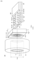
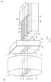
- FIG. 1 is an exploded perspective view for explaining an optical system according to a first embodiment.
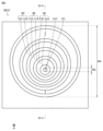
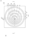
- FIG. FIG. 2 is a front view for explaining the metalens shown in FIG. 1.
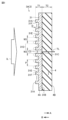
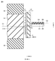
- FIG. FIG. 3 is a cross-sectional view of the metalens and the substrate viewed from arrow III-III in FIG. 2; 1 is a cross-sectional view for explaining an optical system according to Embodiment 1.
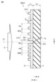
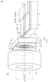
- FIG. FIG. 7 is a front view for explaining a first modification example of the metalens of the optical system according to the first embodiment. 6 is a cross-sectional view of the metalens and the substrate as seen from arrow VI-VI in FIG. 5.
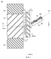
- FIG. FIG. 7 is a cross-sectional view for explaining a first example of an optical system including the metalens shown in FIGS. 5 and 6.
- FIG. FIG. 7 is a cross-sectional view for explaining a second example of an optical system including the metalens shown in FIGS. 5 and 6.
- FIG. 7 is a cross-sectional view for explaining a modification of the metalens shown in FIGS. 5 and 6.
- FIG. 7 is a cross-sectional view for explaining a second modification of the metalens of the optical system according to the first embodiment.
- FIG. FIG. 7 is a cross-sectional view for explaining a third modification of the metalens of the optical system according to the first embodiment.
- FIG. 7 is a cross-sectional view for explaining a fourth modification of the metalens of the optical system according to the first embodiment.
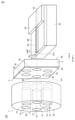
- FIG. 3 is an exploded perspective view for explaining an optical system according to a second embodiment.
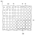
- FIG. 14 is a partially enlarged front view for explaining the metalens shown in FIG. 13.
- FIG. FIG. 15 is a partially enlarged perspective view for explaining the metalens shown in FIGS. 13 and 14.
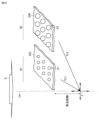
- FIG. 7 is a cross-sectional view for explaining a condensing angle of a metalens of an optical system according to a second embodiment.
- FIG. 7 is an exploded perspective view for explaining an optical system according to a third embodiment.
- 18 is a partially enlarged perspective view for explaining the metalens shown in FIG. 17.
- FIG. FIG. 7 is an exploded perspective view for explaining an optical system according to a fourth embodiment.
- FIG. 7 is an exploded perspective view for explaining an optical system according to a fifth embodiment.
- FIG. 7 is an exploded perspective view for explaining an optical system according to a sixth embodiment.
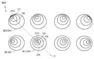
- FIG. 7 is a partially enlarged plan view for explaining an example of a metalens of an optical system according to a sixth embodiment.
- FIG. 7 is an exploded perspective view for explaining a modification of the optical system according to the sixth embodiment.
- FIG. 7 is a diagram for explaining a first example of an optical system according to a seventh embodiment.
- FIG. 7 is a diagram for explaining a second example of an optical system according to Embodiment 7.
- the optical system according to the present embodiment optically connects a first waveguide, a second waveguide whose optical spot size is different from that of the first waveguide, and the first waveguide and the second waveguide. and a metalens.
- light spot size means the width of a region where the light power is 1/e 2 of the maximum value, assuming that the light power distribution of propagating light is Gaussian.
- the first waveguide has a first end face facing the metalens.
- the second waveguide has a second end face facing the metalens.
- the optical spot size at the first end surface of the first waveguide is referred to as the “optical spot size” of the first waveguide.
- the light spot size at the second end surface of the second waveguide will be referred to as the "light spot size” of the second waveguide.
- the optical spot size of the first waveguide is larger than the optical spot size of the second waveguide.
- the term “metalens” refers to a structure that includes at least one metasurface and that condenses light incident from one of the first end surface of the first waveguide and the second end surface of the second waveguide on the other. means body.
- the term “metasurface” refers to a structure consisting of a plurality of electromagnetic wave scatterers arranged in a direction intersecting the direction in which light propagates between a first end face and a second end face.
- the plurality of electromagnetic wave scatterers may be arranged in a direction perpendicular to the propagation direction of light between the first end face and the second end face.
- the plurality of electromagnetic wave scatterers may be arranged in a direction that is inclined at an obtuse angle or an acute angle with respect to the propagation direction of light between the first end face and the second end face.
- the light condensing principle of the metalens according to this embodiment is not particularly limited, typical examples thereof are listed below.
- the metasurface is preferably provided to concentrate light into the micro-aperture and enhance the intensity of the light escaping from the micro-aperture.
- the metalens of the first example has, for example, a bull's eye structured metasurface.
- the metalens of the second example when a metalens with a phase grating is irradiated with light of a target wavelength, the light diffracted at spatially different parts of the phase grating is focused by giving a phase difference to the light.
- the metalens of the second example may include a resonant phase grating provided to provide a phase difference by causing light to resonate with a plurality of fine particles made of, for example, a metal or a dielectric material. Further, the metalens of the second example is provided so as to give a phase difference to light propagating through each of a plurality of dielectric waveguides or metal gap waveguides (MIM (Metal-Insulator-Metal) waveguides). It may also include a waveguide type phase grating.
- MIM Metal-Insulator-Metal
- the optical system according to the present embodiment light at the target wavelength propagates from the first waveguide where the optical spot size is relatively large, through the metalens, to the second waveguide where the optical spot size is relatively small.
- the optical system according to this embodiment is particularly suitable for a configuration in which light propagates from a first waveguide with a relatively large light spot size to a second waveguide with a relatively small light spot size via a metalens.
- the light of the target wavelength may propagate from the second waveguide to the first waveguide through the metalens in the opposite direction to the above.
- the focus of the metalens is on the second end face of the second waveguide, the light emitted from the second end face is enlarged in diameter via the metalens and then transferred to the first end face of the first waveguide. It is emitted as parallel light to the end face side.
- the light spot size at the first end surface of the light propagating from the metalens to the first end surface is referred to as the first light spot size.
- the light spot size at the second end face of the light propagating from the metalens to the second end face is referred to as a second light spot size.
- the difference between the first optical spot size and the optical spot size of the core 1A is as small as possible, and the difference between the second optical spot size and the optical spot size of the Si waveguide 2A is as small as possible. It is designed to be small. In this way, the light transmission efficiency between the first waveguide and the second waveguide is increased.
- the metalens is provided such that the first light spot size is equal to the light spot size of the core 1A, and the second light spot size is equal to the light spot size of the Si waveguide 2A. In this way, the light transmission efficiency between the first waveguide and the second waveguide is maximized.
- the metalens collects the light incident from the first waveguide onto the second waveguide. In other words, the metalens reduces the spot size of the light incident from the first waveguide to the same extent as the second light spot size.
- the metalens causes a process opposite to the former case, and spreads the light incident from the second waveguide to the first waveguide. In other words, the metalens increases the spot size of the light incident from the second waveguide to the same extent as the first light spot size.
- the optical system according to the present embodiment includes a metalens, it is different from a conventional optical system including a polymer waveguide that optically connects the first waveguide and the second waveguide.
- the optical path length between the two waveguides can be shortened.
- planar view means a viewpoint from which the metalens is viewed from the direction in which light propagates between the first waveguide and the second waveguide (hereinafter also referred to as the optical axis direction).
- the arrangement of the plurality of electromagnetic wave scatterers is periodic or non-periodic.
- At least one of the intervals is equal to or less than the wavelength of light propagating through the optical system (hereinafter also referred to as the target wavelength).
- the thickness, width, and interval of each of the plurality of electromagnetic wave scatterers are all equal to or less than the target wavelength.
- the thickness, width, and spacing of each of the plurality of electromagnetic wave scatterers may exceed, for example, the target wavelength. In this case, other parameters among the thickness, width, and spacing of each of the plurality of electromagnetic wave scatterers may be less than the target wavelength. Further, in this case, the thickness, width, or interval of each of the plurality of electromagnetic wave scatterers exceeding the target wavelength is twice or less than the target wavelength.
- the target wavelength is not particularly limited, but is, for example, 300 nm or more and 3 mm or less.
- the optical system is arranged to propagate, for example, visible light, infrared light, and/or terahertz waves.
- the first waveguide according to this embodiment is, for example, the core of an optical fiber.
- the first waveguide is, for example, the core of a single-core fiber or a multi-core fiber.
- the second waveguide according to this embodiment is, for example, a thin wire waveguide, a rib waveguide, or a photonic crystal waveguide.
- an optical system 101 includes an optical fiber 1, a photonics element 2, a metalens 3, and a substrate 4.
- the target wavelength of the optical system 101 is longer than 1100 nm at which basic absorption can occur in silicon (Si), for example, 1260 nm or more and 1565 nm or less.
- the optical fiber 1 is a single-core fiber and includes a core 1A as a first waveguide and a cladding 1B.
- the optical fiber 1 is, for example, a single mode fiber that propagates light of a target wavelength in a single mode.
- the core 1A has a first end surface 1A1 facing the metalens 3.
- the first end surface 1A1 is a plane that intersects with the central axis C1 of the core 1A.
- the first end surface 1A1 is perpendicular to the central axis C1 of the core 1A, for example.
- the shape of the first end surface 1A1 is, for example, circular.
- the cladding 1B covers the core 1A in the circumferential direction with respect to the central axis C1 of the core 1A.
- the refractive index of the material forming the core 1A is higher than the refractive index of the material forming the cladding 1B.
- the dimension (core diameter W1) of the first end surface 1A1 of the core 1A is, for example, 1 ⁇ m or more and 20 ⁇ m or less, preferably 5 ⁇ m or more and 10 ⁇ m or less.
- the optical fiber 1 may be a multimode fiber that propagates light of the target wavelength in multiple modes.
- the core diameter W1 of the core 1A may be, for example, 20 ⁇ m or more and 70 ⁇ m or less.
- Photonics element 2 is a silicon photonics element.
- the photonics element 2 includes a Si waveguide 2A as a second waveguide, a cladding 2B, and a Si substrate 2C.
- the Si waveguide 2A is made of Si.
- the Si waveguide 2A is a so-called thin wire waveguide.
- the Si waveguide 2A has a second end surface 2A1 facing the metalens 3.
- the second end surface 2A1 is a plane that intersects with the central axis C2 of the Si waveguide 2A.
- the second end surface 2A1 is perpendicular to the central axis C2 of the Si waveguide 2A, for example.
- the shape of the second end surface 2A1 is, for example, quadrilateral, preferably square.
- the cladding 2B covers the Si waveguide 2A in the circumferential direction with respect to the central axis C2 of the Si waveguide 2A.
- the material making up the Si waveguide 2A has a higher refractive index than the material making up the cladding 2B.
- the material constituting the Si waveguide 2A includes, for example, Si or silicon nitride (Si 3 N 4 ).
- the cladding 2B includes a first cladding layer 2B1 and a second cladding layer 2B2.
- the first cladding layer 2B1 is placed on the Si substrate 2C, and separates the Si waveguide 2A from the Si substrate 2C.
- the Si waveguide 2A is arranged on the first cladding layer 2B1.
- the second cladding layer 2B2 is placed on each of the Si waveguide 2A and the first cladding layer 2B1.
- the material constituting each of the first cladding layer 2B1 and the second cladding layer 2B2 includes, for example, silicon oxide (SiO 2 ).
- the second cladding layer 2B2 may be an air cladding layer. Note that the entire second cladding layer 2B2 may be an air cladding layer.
- the optical spot size of the Si waveguide 2A is smaller than the optical spot size of the core 1A.
- Each of the width W2 and the thickness T0 of the second end surface 2A1 of the Si waveguide 2A is smaller than the core diameter W1 of the core 1A.
- Each of the width W2 and the thickness To of the Si waveguide 2A is less than 1 ⁇ m, preferably 100 nm or more and less than 500 nm.
- the width W2 of the Si waveguide 2A has a trapezoidal shape, and the width W2 can be long or short, it is preferable that the shorter width satisfies the above-mentioned length, and both the long and short widths should not satisfy the above-mentioned length. More preferred.
- the area of the first end surface 1A1 of the core 1A (hereinafter also referred to as the first area) is larger than the area of the second end surface 2A1 of the Si waveguide 2A (hereinafter also referred to as the second area).
- the ratio of the first area to the second area may be 10 or more, 25 or more, 50 or more, 100 or more, or 500 or more. , 1000 or more.
- the metalens 3 optically connects the first end surface 1A1 of the core 1A and the second end surface 2A1 of the Si waveguide 2A.
- the metalens 3 includes a metasurface 3A with a bull's eye structure.
- the light condensing principle of the metalens 3 of the optical system 101 is the above-mentioned first example.
- the metasurface 3A is formed on the conductor layer 31.
- the conductor layer 31 has a first surface 31A facing the first end surface 1A1 of the core 1A, and a second surface 31B located on the opposite side to the first surface 31A. Each of the first surface 31A and the second surface 31B is perpendicular to, for example, the central axis C1 of the core 1A and the central axis C2 of the Si waveguide 2A.
- the material constituting the conductive layer 31 may be any conductive material as long as surface plasmons can be excited resonantly when light of the target wavelength is incident, but preferably it is an inorganic material, such as , gold, silver, copper, platinum, aluminum or alloys thereof.
- the material constituting the conductor layer 31 preferably contains silver.
- the conductor layer 31 is formed with a through hole 31C as a minute opening.
- the through hole 31C penetrates between the first surface 31A and the second surface 31B.
- the planar shape of the through hole 31C is, for example, circular.
- the through hole 31C is arranged to overlap with the core 1A and the Si waveguide 2A.
- the central axis C3 (hole axis) of the through hole 31C is arranged to overlap with the core 1A and the Si waveguide 2A. More preferably, the central axis C3 of the through hole 31C is arranged on the same straight line as the central axis C1 of the core 1A and the central axis C2 of the Si waveguide 2A.
- a plurality of uneven structures 31D are formed on the first surface 31A of the conductor layer 31.
- the plurality of uneven structures 31D are constituted by a first surface 31A and a plurality of annular grooves 31E recessed with respect to the first surface 31A.
- the conductor layer 31 is formed with a plurality of convex portions 31F (see FIG. 3) that protrude from the bottom surfaces of the plurality of annular grooves 31E and have a first surface 31A.
- each of the plurality of uneven structures 31D is formed in an annular shape so as to surround the through hole 31C.
- the centers of each of the plurality of uneven structures 31D overlap with each other.
- the center of each of the plurality of uneven structures 31D overlaps with the center of the through hole 31C (central axis C3).
- the number of uneven structures 31D is not particularly limited, but may be 3 or more and 30 or less. If the number of uneven structures is small, the range of target wavelengths exhibiting light focusing performance can be widened, and if the number of uneven structures is large, the range of target wavelengths can be narrowed and wavelength selectivity can be improved.
- the surfaces of the plurality of uneven structures 31D that is, the first surface 31A and the wall surfaces and bottom surfaces of the plurality of annular grooves 31E are in contact with air, for example.
- the surface of the plurality of uneven structures 31D may be in contact with any dielectric material.
- the metalens 3 may further include a dielectric film covering the surface of each of the plurality of annular grooves 31E.
- the plurality of uneven structures 31D may be flattened by a dielectric film.
- the outer peripheral edge of the plurality of uneven structures 31D is constituted by, for example, an annular groove 31E.
- the dimensions of the plurality of uneven structures 31D are, for example, equal to each other.
- the width W4 of the outer peripheral edge of the plurality of uneven structures 31D is equal to the core diameter W1 of the core 1A.
- the outer peripheral edge of the plurality of uneven structures 31D may be formed by the first surface 31A.
- the plurality of uneven structures 31D may include a first surface 31A and a plurality of annular convex portions protruding from the first surface 31A.
- the outer peripheral edge of the plurality of uneven structures 31D may be formed by an annular convex portion or may be formed by the first surface 31A.
- the propagation direction of light is not limited.
- Light can propagate along direction A (see FIGS. 1 to 3) from the core 1A, where the optical spot size is relatively large, through the metalens 3, to the Si waveguide 2A, where the optical spot size is relatively small.
- light can propagate from the Si waveguide 2A to the core 1A via the metalens 3 along the direction B (see FIGS. 1 and 3).
- Direction A and direction B are along the horizontal direction, for example. Note that the direction A and the direction B may be along the vertical direction.
- the optical spot size (hereinafter also referred to as first optical spot size) on the first end surface 1A1 of the light propagating from the metalens 3 to the first end surface 1A1 is larger than the optical spot size of the Si waveguide 2A, and preferably the core Equivalent to a light spot size of 1A.
- the optical spot size at the second end surface 2A1 of the light propagating from the metalens 3 to the second end surface 2A1 (hereinafter also referred to as second optical spot size) is smaller than the optical spot size of the core 1A, and preferably Si waveguide. Equivalent to a light spot size of 2A.
- the metalens 3 including the metasurface 3A resonantly excites surface plasmons when light of the target wavelength enters the metasurface 3A from the core 1A, collects the surface plasmons in the through hole 31C as a minute opening, and generates a second light beam. It is provided to emit spot-sized light to the Si waveguide 2A. Further, the metalens 3 is provided so that when light of the target wavelength enters the through hole 31C from the Si waveguide 2A, the light of the first light spot size is emitted to the core 1A by a process opposite to the above process. There is.
- each of the conductor layer 31, the through hole 31C, and the plurality of uneven structures 31D that constitute the metasurface 3A can be arbitrarily selected depending on the target wavelength.
- the thickness T1 (see FIG. 1) of the conductor layer 31 is not particularly limited, but is preferably equal to or less than the target wavelength, more preferably less than the target wavelength, more preferably equal to or less than half the target wavelength, and is 50 nm or more. It may be. When the target wavelength is 1260 nm or more and 1565 nm or less as described above, the thickness T1 may be about 300 nm.
- the hole diameter W3 of the through hole 31C is less than or equal to the target wavelength, and preferably smaller than the target wavelength.
- the hole diameter W3 is, for example, about half the wavelength of interest.
- the width W5 of each of the plurality of annular grooves 31E in the radial direction with respect to the central axis C3 of the through hole 31C and the depth D of each of the plurality of annular grooves 31E are each less than or equal to the target wavelength, preferably smaller than the target wavelength. .
- the width W5 of each of the plurality of annular grooves 31E and the depth D of each of the plurality of annular grooves 31E are, for example, approximately half the value of the target wavelength.
- the distance P between each of the plurality of uneven structures 31D in the radial direction with respect to the central axis C3 of the through hole 31C is not particularly limited, but is equivalent to the target wavelength.
- the interval between the plurality of concavo-convex structures means the pitch (period) between adjacent convex portions or between adjacent concave portions. Specifically, as shown in FIG. 3, it means the interval (width) P of one uneven structure 31D. From the viewpoint of improving light collection performance, it is preferable that the ratio of the distance P between each of the plurality of concavo-convex structures 31D to the target wavelength is 30% or more and 200% or less.
- the ratio of the interval P of each of the plurality of uneven structures 31D to the target wavelength is preferably 140% or less, more preferably 110% or less, and still more preferably less than 100%.
- the ratio of the interval P of each of the plurality of uneven structures 31D to the target wavelength is preferably 60% or more, more preferably more than 65%, and still more preferably 70% or more.
- the ratio (W5/P) of the width W5 of each of the plurality of annular grooves 31E to the interval P of each of the plurality of uneven structures 31D in the radial direction with respect to the central axis C3 of the through hole 31C is not particularly limited, but is 10% or more. % or less. From the viewpoint of further increasing the ratio of transmittance to reflectance of the target wavelength, the ratio W5/P is preferably 30% or more, more preferably 45% or more, even more preferably 60% or more, and particularly preferably 70% or more. , 80% or more is even more particularly preferred.
- the second surface 31B of the metalens 3 is, for example, a flat surface.
- the method for forming the metalens 3 is not particularly limited.
- the metalens 3 may be formed as follows. First, a conductor layer 31 is formed on the third surface 4A of the substrate 4. Any method may be used to form the conductor layer 31, and for example, a sputtering method may be used. Second, the conductor layer 31 is patterned to form a through hole 31C and a plurality of annular grooves 31E. Any method may be used to pattern the conductor layer 31, and may be, for example, photolithography, dry etching, or the like.
- the substrate 4 supports the metalens 3.
- the substrate 4 is transparent to light of the target wavelength.
- the substrate 4 has a third surface 4A in contact with the second surface 31B of the metalens 3, and a fourth surface located on the opposite side to the third surface 4A and facing the second end surface 2A1 of the Si waveguide 2A. 4B.
- the third surface 4A is perpendicular to the central axis C3 of the through hole 31C, for example.
- the substrate 4 is preferably made of a material with a low refractive index from the viewpoint of suppressing Fresnel reflection.
- the substrate 4 may contain, for example, SiO 2 , more preferably contains glass, and is even more preferably made of glass.
- the thickness T2 of the substrate 4 is thicker than the thickness T1 of the conductor layer 31, for example.
- the sum of the thickness T1 of the conductor layer 31 and the thickness T2 of the substrate 4 is the same as that of the polymer required when optically connecting the core 1A and the Si waveguide 2A with a conventional polymer waveguide. shorter than the length of the waveguide.
- Each of the shortest distance L1 and the shortest distance L2 may be shorter than the thickness T1 (see FIG. 3) of the conductor layer 31 of the metalens 3.
- the light propagating through the optical system 101 may pass through the core 1A, the metalens 3, the substrate 4, and the Si waveguide 2A in this order, or may pass through the Si waveguide 2A, the substrate 4, the metalens 3, and the core 1A in this order. You can.
- the optical system 101 includes the metalens 3, the core 1A and the Si waveguide 2A are more connected to each other than an optical system including a polymer waveguide or a convex lens that optically connects the core 1A and the Si waveguide 2A.
- the optical path length between the two can be shortened.
- the relative positions of each of the core 1A, the Si waveguide 2A, and the metalens 3 are caused by manufacturing errors. Even in the case where the waveguide 2A varies, the light transmission efficiency between the core 1A and the Si waveguide 2A is not likely to decrease.
- the focal position of the optical lens changes relative to the Si waveguide. There is a risk that the transmission efficiency may significantly decrease due to large fluctuations.
- the metalens 3 since the metalens 3 is formed with the through-hole 31C, the light incident on the metalens 3 from the core 1A or the Si waveguide 2A is concentrated on the through-hole 31C, and then passes through the through-hole 31C. To Penetrate.
- the focal point of the light emitted from the metalens 3 to the Si waveguide 2A or the core 1A is formed in the through hole 31C, and it can be assumed that parallel light is incident on the Si waveguide 2A or the core 1A. can.
- the light transmission efficiency between the first waveguide and the second waveguide is determined by the shortest distance L1 between the core 1A and the metalens 3 and between the Si waveguide 2A and the substrate 4.
- the shortest distance L2 between them is not easily affected by variations due to manufacturing errors and the like.
- the direction A or the direction B in which light propagates in the optical system 101 may be any direction, and may be along the horizontal direction or the vertical direction, for example. According to the optical system 101, even when the first end surface 1A1 of the optical fiber 1 and the second end surface 2A1 of the Si waveguide 2A face each other in the horizontal direction, the direction of propagation of light is not changed by a mirror or the like, and both can be connected. can be optically connected. Therefore, the degree of freedom in designing the optical system 101 is higher than that of conventional optical systems.
- a plurality of concavo-convex structures 31D are formed to surround the through-hole 31C of the metalens 3.
- surface plasmons that are resonantly excited gather at the through-holes 31C.
- the light transmitted through the metalens 3 can be collected more efficiently, and the intensity of the light becomes higher.
- the propagation direction of the light IL entering the metalens 3 from the core 1A is set in a direction perpendicular to the first surface 31A.
- the propagation direction of the light TL emitted from the metalens 3 to the Si waveguide 2A is parallel to the propagation direction of the light IL entering the metalens 3 from the core 1A.
- the propagation direction of the light IL entering the metalens 3 from the Si waveguide 2A is set to be perpendicular to the second surface 31B.
- the propagation direction of the light emitted from the metalens 3 to the core 1A is parallel to the propagation direction of the light IL entering the metalens 3 from the Si waveguide 2A.
- the metalens 3 may be made of an inorganic material.
- the heat resistance of the optical system 101 is high compared to optical systems comprising polymer waveguides.
- the optical system 101 may include the metalens 3 shown in FIGS. 5 and 6 instead of the metalens 3 shown in FIGS. 1 to 4.
- the metalens 3 shown in FIGS. 5 and 6 has basically the same configuration as the metalens 3 shown in FIGS. 1 to 4, but includes a metasurface 3B instead of the metasurface 3A. This is different from the metalens 3 shown in FIG.
- the metasurface 3B is different from the metasurface 3A in that the center of each of the plurality of uneven structures 31D is arranged so as not to overlap the center (central axis C3) of the through hole 31C (micro opening) in plan view. different.
- the metasurface 3B also has a bull's eye structure like the metasurface 3A.
- the following will mainly explain the differences between the metalens 3 and the metasurface 3B shown in FIGS. 5 and 6 from the metalens 3 and the metasurface 3B shown in FIGS. 1 to 4.
- the interval (period) of each part of the plurality of uneven structures 31D located on one side with respect to the through hole 31C in the direction C perpendicular to the central axis C3 of the through hole 31C is wider than the interval (period) of each part of the plurality of uneven structures 31D located on the other side with respect to the through hole 31C.
- the interval between the respective parts of the plurality of uneven structures 31D, which are located on one side of the through hole 31C in the direction C and are arranged at relatively wide intervals will also be referred to as a first interval PA. do.
- the interval between each portion of the plurality of uneven structures 31D, which are located on the other side of the through hole 31C in the direction C and are arranged at relatively narrow intervals, is also referred to as a second interval PB.
- the first interval PA of each portion of the plurality of uneven structures 31D located on one side with respect to the through hole 31C gradually becomes wider as the distance from the through hole 31C increases.
- the second spacing PB of each portion of the plurality of uneven structures 31D located on the other side with respect to the through hole 31C is, for example, equal to each other.
- the width of each portion of the plurality of annular grooves 31E located on one side with respect to the through hole 31C in the first direction C perpendicular to the central axis C3 of the through hole 31C (hereinafter also referred to as the first width W5A). ) is wider than the width (hereinafter also referred to as second width W5B) of each portion of the plurality of annular grooves 31E located on the other side with respect to the through hole 31C.
- the first width W5A of each portion of the plurality of annular grooves 31E located on one side with respect to the through hole 31C gradually becomes wider as the distance from the through hole 31C increases.
- the second width W5B of each portion of the plurality of annular grooves 31E located on the other side with respect to the through hole 31C is, for example, equal to each other.
- the plurality of uneven structures 31D may have a region where the ratio of the interval P to the target wavelength is 30% or more and 200% or less.
- the ratio of the first interval PA of each of the plurality of uneven structures 31D to the target wavelength may be, for example, 200% or less, preferably 140% or less, more preferably 110% or less, and even more preferably 100% or less. less than %.
- the ratio of the second interval PB of each of the plurality of uneven structures 31D to the target wavelength may be 30% or more, preferably 60% or more, more preferably more than 65%, and still more preferably It is 70% or more.
- the ratio of the first width W5A to the first spacing PA (W5A/PA) and the ratio of the second width W5B to the second spacing PB (W5B/PB) are not particularly limited, but should be 10% or more and 95% or less. It's fine. From the viewpoint of further increasing the ratio of transmittance to reflectance of the target wavelength, each of the ratio W5A/PA and the ratio W5B/PB is preferably 30% or more, more preferably 45% or more, and even more preferably 60% or more. Preferably, 80% or more is particularly preferable.
- the propagation direction of the light IL entering the metalens 3 from the core 1A is set in a direction perpendicular to the first surface 31A.
- the propagation direction of the light TL emitted from the metalens 3 to the Si waveguide 2A is inclined with respect to the propagation direction of the light IL incident on the metalens 3 from the core 1A. Therefore, as shown in FIG. 7, the metalens 3 including the metasurface 3B is suitable for an optical system in which the central axis C2 of the Si waveguide 2A is inclined toward the first direction C with respect to the central axis C1 of the core 1A. It is. Further, as shown in FIG.
- the central axis C2 of the Si waveguide 2A is parallel to the central axis C1 of the core 1A, but the central axis C1 is centered in the first direction C. It is also suitable for optical systems spaced apart from axis C2. In each of the optical systems shown in FIGS. 7 and 8, the light transmission efficiency between the core 1A and the Si waveguide 2A is also high.
- FIGS. 7 and 8 illustrate the output angle ⁇ 1 of the metalens 3 including the metasurface 3B having a bull's eye structure.
- the output angle ⁇ 1 in FIG. 7 is the angle (first angle) that the central axis C2 of the Si waveguide 2A makes with the central axis C3 of the through hole 31C (C3 coincides with C1 in FIG. 7).
- the emission angle ⁇ 1 in FIG. 8 is the intersection of the central axis C3 of the through hole 31C (C3 coincides with C1 in FIG. 8) and the third surface 4A of the substrate 4 (on the second surface 31B of the metasurface 3B).
- the intersection of the central axis C2 of the Si waveguide 2A and the second end surface 2A1 of the Si waveguide 2A (the end of the central axis C3 of the through hole 31C located on the second end surface 2A1 of the Si waveguide 2A) This is the angle that the straight line connecting the central axis C2 of the Si waveguide 2A (the end of the central axis C2) and the central axis C3 of the through hole 31C forms.
- the exit angle ⁇ 1 of the metalens 3 including the metasurface 3B is not particularly limited, but may be, for example, 3° or more and 60° or less, and may be 45° or less.
- the output angle ⁇ 1 may be 7° or more, 16° or more, 30° or more, or 40° or more.
- the distances (hereinafter also referred to as shift amounts) between the centers of the plurality of uneven structures 31D may be equal to each other.
- each shift amount is referred to as a unit shift amount S.
- the ratio ( ⁇ 1 /S) of the output angle ⁇ 1 to the unit shift amount S may be 0.19 or more, or 0.58 or more. It may be 2.00 or more, 3.33 or more, 6.00 or more, or 10.00 or more.
- the first intervals PA are, for example, equal to each other.
- the ratio of the first interval PA of each of the plurality of uneven structures 31D to the target wavelength may be, for example, 200% or less, preferably 140% or less, and more Preferably it is 110% or less, more preferably less than 100%.
- the ratio of the first interval PA of each of the plurality of uneven structures 31D to the target wavelength may be 30% or more, preferably 60% or more, more preferably more than 65%, and still more preferably It is 70% or more. Note that the first interval PA may gradually become wider as the distance from the through hole 31C increases.
- the present inventors have determined that when the output angle ⁇ 1 to be achieved in the metasurface 3B is 5° or more, the unit shift amount S (unit: nm) of the metasurface 3B and the above-mentioned interval P of the plurality of uneven structures 31D (Unit: nm) It was confirmed that the above-mentioned output angle ⁇ 1 can be achieved if the angle is set so that the following relational expression (1) is satisfied.
- the optical system 101 may include a metalens 3 shown in FIG. 10 instead of the metalens 3 shown in FIGS. 1 to 6.
- the metalens 3 shown in FIG. 10 has basically the same configuration as the metalens 3 shown in FIGS. 1 to 6, except that it further includes a metasurface 3A disposed on the fourth surface 4B of the substrate 4. , which is different from the metalens 3 shown in FIGS. 1 to 6.
- the metasurface 3A disposed on the fourth surface 4B is symmetrical with respect to the substrate 4 with respect to the metasurface 3A disposed on the third surface 4A.
- the metalens 3 of the optical system 101 only needs to include the metasurface 3A or the metasurface 3B disposed on at least one of the third surface 4A and the fourth surface 4B of the substrate 4.
- the optical system 101 may include the metalens 3 shown in FIG. 11 or 12 instead of the metalens 3 shown in FIGS. 1 to 6.
- the metalens 3 shown in FIG. 11 has basically the same configuration as the metalens 3 shown in FIGS. 1 to 6, but each of the plurality of annular grooves 31E in the plurality of uneven structures 31D is It differs from the metalens 3 shown in FIGS. 1 to 6 in that it is formed so as to penetrate between the first surface 31A and the second surface 31B and expose a part of the third surface 4A of the substrate 4. .
- the bottom surface of each annular groove 31E is formed by the third surface 4A of the substrate 4.
- the metalens 3 shown in FIG. 11 has basically the same configuration as the metalens 3 shown in FIGS.
- 1 to 6 is composed of a surface 4A and a plurality of convex portions 31F formed on the third surface 4A of the substrate 4 as an island-like pattern separated from each other. It is different from.
- the depth of each of the plurality of annular grooves 31E is equal to the depth of the through hole 31C.
- the metalens 3 shown in FIG. 12 has basically the same configuration as the metalens 3 shown in FIGS. 1 to 6, but a plurality of It differs from the metalens 3 shown in FIGS. 1 to 6 in that a concavo-convex structure is formed.
- the plurality of uneven structures 31G formed on the second surface 31B are arranged on the first surface 31A with respect to a virtual symmetrical plane located on the midpoint between the first surface 31A and the second surface 31B. It is in a plane symmetrical relationship with the plurality of concavo-convex structures 31D that are formed.
- the plurality of uneven structures 31G are constituted by a second surface 31B and a plurality of annular grooves 31H recessed with respect to the second surface 31B.
- the conductor layer 31 is formed with a plurality of protrusions 31I that protrude from the bottom surfaces of the plurality of annular grooves 31H and have a second surface 31B.
- Each convex portion 31I is arranged to overlap with each convex portion 31F, for example, in a direction orthogonal to the first surface 31A.
- the second surface 31B and the walls and bottom surfaces of the plurality of annular grooves 31E formed on the second surface 31B are in contact with the third surface 4A of the substrate 4.
- the width of each of the plurality of annular grooves 31H is equal to the width W5 of the plurality of annular grooves 31E.
- the metalens 3 shown in FIG. 12 is formed by, for example, forming a plurality of convex portions 31I in the recessed portions of the third surface 4A of the substrate 4, and then forming the remainder of the conductor layer 31 on the third surface 4A. , can be manufactured.
- the optical system 102 according to the second embodiment will be described with reference to FIG. 13.
- the optical system 102 according to the second embodiment has basically the same configuration as the optical system 101 according to the first embodiment and has the same effects, but the metalens 3 is arranged on the third surface 4A of the substrate 4. It differs from the optical system 101 in that it includes a phase grating that provides a phase difference to light of the target wavelength.
- the differences between the optical system 102 and the optical system 101 will be mainly explained.
- the metalens 3 of the optical system 102 includes a waveguide type phase grating.
- the light focusing principle of the metalens 3 of the optical system 102 is the same as the second example above.
- the metalens 3 includes a plurality of columnar bodies 32 (convex portions) arranged at intervals on the third surface 4A and a filling portion 33 that fills the spaces between the plurality of columnar bodies 32. It includes a metasurface 3C composed of.
- the refractive index of the material constituting each of the plurality of columnar bodies 32 is higher than the refractive index of the material constituting the filling part 33.
- the outer shape of each of the plurality of columnar bodies 32 is, for example, cylindrical.
- the central axis of each of the plurality of columnar bodies 32 is parallel to the central axis C1 of the core 1A.
- each of the plurality of columnar bodies 32 is perpendicular to the third surface 4A of the substrate 4, for example.
- the material constituting the plurality of columnar bodies 32 and the material constituting the filling part 33 are not particularly limited as long as their respective refractive indices satisfy the above relationship.
- the material constituting the plurality of columnar bodies 32 is, for example, a dielectric material, more preferably an inorganic material, and includes Si as a specific example.
- the surfaces of the plurality of columnar bodies 32 are in contact with an air layer serving as the filling portion 33, for example.
- the filling portion 33 may be formed of a dielectric film.
- the surfaces of the plurality of columnar bodies 32 may be in contact with a dielectric film.
- the plurality of columnar bodies 32 may be embedded in the filling part 33.
- the metalens 3 may further include a base material 34 that is transparent to light of the target wavelength and is disposed on the third surface 4A of the substrate 4.
- Each of the plurality of columnar bodies 32 may be fixed to the base material 34. Note that the metalens 3 may not include the base material 34, and each of the plurality of columnar bodies 32 may be fixed to the third surface 4A of the substrate 4.
- Each of the plurality of columnar bodies 32 forms a waveguide through which light of the target wavelength propagates.
- the phase of the light incident on each of the plurality of columnar bodies 32 changes during the process of propagating through each columnar body 32.
- the amount of change in the phase of light propagating through each columnar body 32 is the ratio D of the outer diameter D (maximum width) of the columnar body 32 to the distance P (pitch) between the columnar body 32 and another adjacent columnar body 32. The larger /P is, the more.
- the position of the focal point F (see FIG. 15) of the metalens 3 changes depending on the spatial distribution of the phase of the light that has passed through each waveguide. Therefore, the amount of change in the phase of the light propagating through each columnar body 32 may be arbitrarily set according to the position where the focal point F of the metalens 3 is to be placed.
- At least one of the outer diameter and height of each of the plurality of columnar bodies 32 and the interval between two adjacent columnar bodies 32 is continuous or stepped in the radial direction depending on the distance to the focal point. It is set up so that it changes over time.
- At least one of the outer diameter of the columnar body 32 and the interval between two adjacent columnar bodies 32 changes continuously or stepwise depending on the distance to the focal point. It is preferable. More preferably, in a plan view, both the outer diameter of the columnar body 32 and the interval between two adjacent columnar bodies 32 change continuously or stepwise depending on the distance to the focal point.
- the outer diameter of each of the plurality of columnar bodies 32 increases as the distance from the focal point F of the metalens 3 increases in plan view.
- the distance between two adjacent columnar bodies 32 is provided such that the farther from the focal point F of the metalens 3, the smaller the distance between them.
- the metalens 3 has a first region R1 in which the plurality of columnar bodies 32 are arranged such that the amount of change in phase is relatively small. and a second region R2 in which a plurality of columnar bodies 32 are arranged so as to increase in size.
- the first region R1 is a region closer to the focal point F than the second region R2.
- the ratio D2/P2 of the outer diameter D2 of the second group of columnar bodies 32B to the interval P2 between the second group of columnar bodies 32B formed in the second region R2 is the ratio D2/P2 of the second group of columnar bodies 32B formed in the second region R2.
- the amount of change in the phase of the light TL2 that has propagated through each of the columnar bodies 32B of the second group is greater than the amount of change in the phase of the light TL1 that has propagated through each of the columnar bodies 32A of the first group.
- the focal point F is arranged on the same straight line as the central axis C4 of the phase grating of the metalens 3, at least one of the outer diameter of the columnar body 32 and the interval between two adjacent columnar bodies 32 is It suffices if it changes continuously or stepwise depending on the distance to the central axis C4.
- the outer diameter of each of the plurality of columnar bodies 32 increases as the distance from the central axis C4 of the metalens 3 increases, and the distance between two adjacent columnar bodies 32 decreases as the distance from the central axis C4 of the metalens 3 increases. It may be provided as follows.
- the outer diameter of each of the plurality of columnar bodies 32 is equal to or less than the target wavelength.
- the outer diameter of each of the plurality of columnar bodies 32 is, for example, several tens of nm or more and 1 ⁇ m or less.
- the distance between two adjacent columnar bodies 32 is equal to or less than the target wavelength.
- the interval between two adjacent columnar bodies 32 is, for example, several tens of nanometers or more and 1.55 ⁇ m or less. Note that the interval between two adjacent columnar bodies 32 means the distance between the central axes of two adjacent columnar bodies 32.
- the height H2 of the second group of columnar bodies 32B is, for example, lower than the height H1 of the first group of columnar bodies 32B. Note that the height H2 of the second group of columnar bodies 32B may be equal to the height H1 of the first group of columnar bodies 32B, for example.
- the maximum height of each of the plurality of columnar bodies 32 is shorter than the thickness of a convex lens for optically connecting the core 1A and the Si waveguide 2A.
- the maximum height of each of the plurality of columnar bodies 32 is, for example, 2 ⁇ m or less, and may be 1 ⁇ m or less.
- structures in which at least one of the outer diameter and height of the columnar body 32 and the interval between two adjacent columnar bodies 32 change continuously or stepwise depending on the distance to the focal point include those shown in FIGS. 15, in which at least one of the outer diameter and height of a columnar body 32 and the interval between two adjacent columnar bodies 32 change monotonically, such a structure is also referred to as a unit (hereinafter referred to as a structure A periodic structure in which the structural units are periodically arranged in the radial direction with respect to the central axis C4 of the phase grating is included.
- the structural units in which at least one of the height, maximum width, and pitch of each of the plurality of columnar bodies 32 changes continuously or stepwise are periodically arranged in the radial direction. It may have a periodic structure arranged symmetrically.
- the shortest distance between the first end surface 1A1 of the core 1A and the metalens 3 is preferably as short as possible.
- the shortest distance between the Si waveguide 2A and the metalens 3 is preferably a value as close to the focal length f as possible, and more preferably equal to the focal length f.
- the optical path length between the first end surface 1A1 of the core 1A and the second end surface 2A1 of the Si waveguide 2A in the optical system 102 is determined when the core 1A and the Si waveguide 2A are optically connected by a polymer waveguide or a convex lens. can be shorter compared to optical systems with
- the propagation direction of light is not limited.
- the light may propagate from the core 1A, where the optical spot size is relatively large, through the metalens 3, to the Si waveguide 2A, where the optical spot size is relatively small, or in the opposite direction, through the Si waveguide 2A, where the optical spot size is relatively small. It may also propagate from 2A to the core 1A via the metalens 3.
- the method of forming the metalens 3 of the optical system 102 is also not particularly limited.
- the plurality of columnar bodies 32 of the metalens 3 may be formed by forming a dielectric film on the third surface 4A of the substrate 4 and then patterning the dielectric film. For example, a photoresist is applied onto a dielectric film formed on the third surface 4A of the substrate 4, and the photoresist is exposed and developed through a mask with a pattern drawn thereon, and then the dielectric film is coated using the photoresist as a mask. It may be formed by etching. Further, the plurality of columnar bodies 32 may be formed by, for example, a screen printing method.
- the optical path length between the core 1A and the Si waveguide 2A which is limited by the thickness and depth of focus of the metalens 3, is determined by the polymer waveguide that can optically connect the core 1A and the Si waveguide 2A. or the sum of the thickness and depth of focus of a convex lens that can optically connect the core 1A and the Si waveguide 2A.
- the degree of freedom in designing the focal position is higher, and the depth of focus and the propagation direction of light can be easily changed.
- the metalens 3 of the optical system 102 only needs to be placed on the third surface 4A or fourth surface 4B of the substrate 4.
- a structure in which at least one of the outer diameter and height of the columnar body 32 and the interval between two adjacent columnar bodies 32 changes continuously or stepwise depending on the distance to the focal point has the structure shown in FIG. 14 and 15, in which the outer diameter and height of the columnar bodies 32 and/or the interval between two adjacent columnar bodies 32 change monotonically, as well as structures in which such a structure is used as a structural unit.
- Each structural unit includes the first region R1 and the second region R2.
- the amount of change in the phase of each columnar body 32 in each structural unit is within the range of 0 to 2 ⁇ .
- the width of each structural unit in the radial direction may be set so that
- the width of each structural unit in the radial direction required for the amount of change in phase to be 2 ⁇ in each structural unit becomes narrower as the distance from the central axis C4 increases.
- the width in the radial direction of the first structural unit located closest to the central axis C4 of the phase grating is the second closest to the central axis C4 of the phase grating.
- the width in the radial direction of the second structural unit at the position is set to be wider than the width in the radial direction.
- the width of each structural unit in the radial direction required for the amount of change in phase to be 2 ⁇ in each structural unit changes depending on the diameter of the metalens 3.
- the width of the first structural unit in the radial direction required for the amount of phase change to be 2 ⁇ in the first structural unit is 1.00 ⁇ m or more.3. It is preferable that it is 50 ⁇ m or less.
- the width of the first structural unit in the radial direction required for the amount of phase change to be 2 ⁇ in the first structural unit is 2.00 ⁇ m or more.5. It is preferable that it is 00 ⁇ m or less.
- the width of the first structural unit in the radial direction required for the amount of phase change to be 2 ⁇ in the first structural unit is 3.00 ⁇ m or more7. It is preferable that it is 00 ⁇ m or less.
- the focal length f (unit: nm) of the metalens 3 including the phase grating, the condensing angle ⁇ 2 of the metalens 3, and the radius R (unit: nm) of the metalens 3 satisfy the following relational expression (2).
- FIG. 16 shows the focal length f, radius R, and condensing angle ⁇ 2 of the metalens 3 including the metasurface 3C.
- the condensing angle ⁇ 2 shown in FIG. 16 is the angle that the first virtual straight line VL1 makes with the second virtual straight line VL2.
- the first virtual straight line VL1 indicates the course of light that has propagated through the columnar body 32 located at the outermost position in the radial direction with respect to the central axis C4 among the plurality of columnar bodies 32.
- the first imaginary straight line VL1 connects the outermost end of the columnar body 32 located at the outermost position in the radial direction on the third surface 4A side of the substrate 4, the central axis C2 of the Si waveguide 2A, and the second end surface 2A1.
- the second virtual straight line VL2 is a virtual straight line connecting the intersection between the central axis C3 of the metasurface 3C and the third surface 4A of the substrate 4 and the intersection between the central axis C2 of the Si waveguide 2A and the second end surface 2A1. .
- the second virtual straight line VL2 is arranged on the same straight line.
- the condensing angle ⁇ 2 of the metalens 3 including the metasurface 3C is, for example, 20° or more and 70° or less, preferably 30° or more and 60° or less.
- the length of the second virtual straight line VL2 is equal to the focal length f. If the condensing angle ⁇ 2 is 30° or more and 60° or less, the numerical aperture NA of the metalens 3 becomes smaller and the depth of focus becomes deeper, compared to the case where the condensing angle ⁇ 2 is 70°, so the optical axis It is easy to adjust the position of the metalens 3 with respect to the Si waveguide 2A in the direction.
- the numerical aperture NA of the metalens 3 is calculated by multiplying the sine (Sin ⁇ 2 ) of the condensing angle ⁇ 2 of the metalens 3 by the refractive index n of the medium existing between the metalens 3 and the Si waveguide 2A. .
- the numerical aperture NA is preferably 0.5 or more, more preferably 0.7 or more.
- the Si waveguide 2A has a large numerical aperture (spreading of light) due to a large relative refractive index difference between Si forming the core and SiO 2 forming the cladding.
- the numerical aperture NA of the metalens 3 is as large as the numerical aperture of the Si waveguide 2A.
- the material forming the plurality of columnar bodies 32 may be metal.
- the phase grating of the metalens 3 may include a plurality of MIM waveguides instead of a plurality of dielectric waveguides.
- the optical system 103 according to Embodiment 3 will be described with reference to FIG. 17.
- the optical system 103 according to the third embodiment has basically the same configuration as the optical system 102 according to the second embodiment and has the same effect, but the metalens 3 is not a waveguide type phase grating but a resonance side phase grating. It differs from optical system 102 in that it includes: Hereinafter, the differences between the optical system 103 and the optical system 102 will be mainly explained.
- the metalens 3 includes a plurality of spherical bodies 35 (convex parts) arranged at intervals on the third surface 4A and a filling part 33 filling the spaces between the plurality of spherical bodies 35. including a metasurface 3D with .
- the material constituting the plurality of spherical bodies 35 is, for example, a dielectric.
- the material forming the filling portion 33 is, for example, air.
- the filling portion 33 may be made of a dielectric film.
- the surfaces of the plurality of spherical bodies 35 may be in contact with a dielectric film.
- the plurality of spherical bodies 35 may be embedded in the filling part 33.
- Each of the plurality of spherical bodies 35 is provided so as to have Mie resonance with the light of the target wavelength.
- the phase of the light incident on each of the plurality of spherical bodies 35 changes in the process of scattering the light due to resonance.
- the wavelength of the light incident on each spherical body 35 is not too long compared to the wavelength of light that resonates with each spherical body 35 (resonance wavelength)
- the wavelength of light that resonates with each spherical body 35 resonate wavelength
- the longer the wavelength of the light incident on the spherical bodies 35 the greater the amount of change in the phase of the light scattered by each spherical body 35.
- the amount of change in the phase of the light scattered by each spherical body 35 increases as the outer diameter D of the spherical body 35 increases.
- the position of the focal point F (see FIG. 18) of the metalens 3 changes depending on the spatial distribution of the phase of the light scattered by each spherical body 35. Therefore, the amount of change in the phase of the light scattered by each spherical body 35 may be arbitrarily set depending on the position where the focal point F of the metalens 3 is to be placed.
- the outer diameter of the spherical body 35 changes continuously or stepwise depending on the distance to the focal point.
- the outer diameter of each of the plurality of spherical bodies 35 increases as the distance from the focal point F of the metalens 3 increases in plan view.
- the metalens 3 has a first region R1 where a plurality of spherical bodies 35 are arranged such that the amount of change in phase is relatively small, and a first region R1 where the amount of change in phase is relatively large. and a second region R2 in which a plurality of spherical bodies 35 are arranged.
- the first region R1 is a region closer to the focal point F than the second region R2.
- the outer diameter D2 of the second group of spherical bodies 35 formed in the second region R2 is larger than the outer diameter D1 of the first group of spherical bodies 35A formed in the first region R1.
- the amount of change in the phase of the light TL2 scattered by each of the second group of spherical bodies 35B is greater than the amount of change in the phase of the light TL1 scattered by each of the first group of spherical bodies 35A.
- the outer diameter of the spherical body 35 is continuous or stepwise in plan view depending on the distance to the central axis C4. It suffices if it changes accordingly.
- the outer diameter of each of the plurality of spherical bodies 35 is equal to or less than the target wavelength.
- the outer diameter of each of the plurality of spherical bodies 35 is, for example, several tens of nanometers or more and 1 ⁇ m or less.
- the shortest distance between the first end surface 1A1 of the core 1A and the metalens 3 is preferably as short as possible.
- the shortest distance between the Si waveguide 2A and the metalens 3 is preferably a value as close to the focal length f as possible, and more preferably equal to the focal length f.
- the optical path length between the first end surface 1A1 of the core 1A and the second end surface 2A1 of the Si waveguide 2A in the optical system 103 is such that the core 1A and the Si waveguide 2A are optically connected by a polymer waveguide or a convex lens. can be shorter compared to optical systems with
- the propagation direction of light is not limited.
- the light may propagate from the core 1A, where the optical spot size is relatively large, through the metalens 3, to the Si waveguide 2A, where the optical spot size is relatively small, or in the opposite direction, through the Si waveguide 2A, where the optical spot size is relatively small. It may also propagate from 2A to the core 1A via the metalens 3.
- the method of forming the metalens 3 of the optical system 103 is also not particularly limited.
- the plurality of spherical bodies 35 of the metalens 3 can be formed, for example, by a known nanoparticle manufacturing method.
- the optical path length between the core 1A and the Si waveguide 2A which is limited by the thickness and depth of focus of the metalens 3, is determined by the polymer waveguide that can optically connect the core 1A and the Si waveguide 2A. or the sum of the thickness and depth of focus of a convex lens that can optically connect the core 1A and the Si waveguide 2A.
- the optical system 103 has a higher degree of freedom in designing the focal position than an optical system including a convex lens, and can easily change the depth of focus and the propagation direction of light.
- the metalens 3 of the optical system 103 only needs to be placed on the third surface 4A or fourth surface 4B of the substrate 4.
- the material constituting the plurality of spherical bodies 35 may be metal.
- each of the plurality of spherical bodies 35 is provided so as to have plasmon resonance with the light of the target wavelength.
- the phase of the light incident on each of the plurality of spherical bodies 35 changes as the light resonates with each spherical body 35 and is scattered.
- the spherical body 35 made of metal, as well as the spherical body 35 made of dielectric the larger the outer diameter D of the spherical body 35, the greater the amount of change in the phase of light.
- the principle by which the phase of light scattered by the spherical body 35 changes differs depending on the material that constitutes the spherical body 35, but there is a tendency that the larger the outer diameter D of the spherical body 35, the greater the amount of change in the phase of the light. This is the same regardless of the material of which the spherical body 35 is made.
- the metalens 3 of the optical system 103 can also be deformed similarly to the metalens 3 of the optical system 102.
- the outer diameter of the spherical body 35 In addition to the structure in which at least one of the height and the interval between two adjacent spherical bodies 35 changes monotonically, such a structure is used as a structural unit, and the structural unit is the radial direction with respect to the central axis C4 of the phase grating. contains periodic structures that are arranged periodically.
- optical system 104 according to Embodiment 4 will be described.
- the optical system 104 according to the fourth embodiment has basically the same configuration as the optical systems 101 to 103 of any of the first to third embodiments and has the same effects, but the second waveguide is a thin wire waveguide. It differs from the optical systems 101 to 103 in that it is a photonic crystal waveguide rather than a photonic crystal waveguide. The following will mainly explain the differences between the optical system 104 and the optical systems 101 to 103.
- the photonics element 2 includes a crystal slab 2D, a first cladding layer 2B1, and a second cladding layer 2B2.
- the second waveguide is part of the crystal slab 2D.
- the crystal slab 2D has two regions 2D1 and 2D2 in which a plurality of through holes 2E are formed, and a region 2D3 sandwiched between these two regions 2D1 and 2D2 in which a plurality of through holes 2E are not formed. are doing.
- the material constituting the crystal slab 2D includes, for example, at least one selected from the group consisting of polytetrafluoroethylene (PTFE), polyimide, and cyclic olefin polymer (COP).
- PTFE polytetrafluoroethylene
- COP cyclic olefin polymer
- the opening shape of the plurality of through holes 2E is, for example, circular.
- the centers of each of the plurality of through holes 2E are arranged to form lattice points of a regular hexagonal lattice.
- the hole diameter of each of the plurality of through holes 2E and the interval between two adjacent through holes 2E are set so that light of the target wavelength does not propagate through the region 2D1 and the region 2D2. From a different perspective, the hole diameter of each of the plurality of through holes 2E and the interval between two adjacent through holes 2E are set such that the region 2D3 where no through hole 2E is formed forms a photonic crystal waveguide. There is.
- the first cladding layer 2B1 and the second cladding layer 2B2 are arranged to sandwich the crystal slab 2D.
- the refractive index of the material forming each of the first cladding layer 2B1 and the second cladding layer 2B2 is lower than the refractive index of the material forming the crystal slab 2D.
- the material constituting each of the first cladding layer 2B1 and the second cladding layer 2B2 includes, for example, SiO 2 . Note that one or both of the first cladding layer 2B1 and the second cladding layer 2B2 may be an air layer.
- the optical system 104 is provided to propagate, for example, terahertz waves.
- the target wavelength of the optical system 104 is, for example, 30 ⁇ m or more and 3 mm or less.
- the optical fiber 1 is a metal hollow optical fiber and may include a hollow portion 1C, a metal layer 1D, and a cladding 1B.
- the hollow portion 1C is filled with air.
- the metal layer 1D has an inner circumferential surface facing the hollow portion 1C and an outer circumferential surface in contact with the inner circumferential surface of the cladding 1B.
- the material constituting the metal layer 1D is not particularly limited, but includes silver (Ag), for example.
- the thickness of the metal layer 1D is, for example, several nm or more and several 100 nm or less.
- the outer diameter of the metal layer 1D is, for example, 1 mm or less.
- the propagation direction of light is not limited.
- the light may propagate from the core 1A, where the optical spot size is relatively large, through the metalens 3, to the Si waveguide 2A, where the optical spot size is relatively small, or in the opposite direction, through the Si waveguide 2A, where the optical spot size is relatively small. It may also propagate from 2A to the core 1A via the metalens 3.
- the optical system 104 is suitable for propagating terahertz waves.
- the material constituting the crystal slab 2D includes at least one selected from the group consisting of polytetrafluoroethylene (PTFE), polyimide, and cyclic olefin polymer (COP) as described above.
- the light propagated by the optical system 104 is not limited to terahertz waves.
- the target wavelength of the optical system 104 may be shorter than the terahertz wave, and in this case, the material forming the crystal slab 2D may be Si.
- optical system 105 according to Embodiment 5 With reference to FIG. 20, optical system 105 according to Embodiment 5 will be described.
- the optical system 105 according to the fifth embodiment has basically the same configuration as the optical systems 101 to 103 of any of the first to third embodiments and has the same effect, but the Si waveguide 2A is a thin wire waveguide. It differs from the optical systems 101 to 103 in that it is a rib-type waveguide rather than a rib-type waveguide. The following will mainly explain the differences between the optical system 105 and the optical systems 101 to 103.
- the Si waveguide 2A has a relative width in a direction perpendicular to the stacking direction of the Si substrate 2C, the first cladding layer 2B1, the Si waveguide 2A, and the second cladding layer 2B2, and the extending direction of the Si waveguide 2A. It has a slab part 21 that is relatively wide, and a ridge part 22 that protrudes from the slab part 21 to the side opposite to the first cladding layer 2B1 and has a relatively narrow width in that direction. In the optical system 105, the ridge portion 22 and a portion of the slab portion 21 located near the ridge portion 22 constitute the Si waveguide 2A.
- the propagation direction of light is not limited.
- the light may propagate from the core 1A, where the optical spot size is relatively large, through the metalens 3, to the Si waveguide 2A, where the optical spot size is relatively small, or in the opposite direction, through the Si waveguide 2A, where the optical spot size is relatively small. It may also propagate from 2A to the core 1A via the metalens 3.
- the photonics element 2 may have a PIN structure. Specifically, when viewed from the stacking direction of the slab portion 21 and the ridge portion 22, the slab portion 21 has a p-type impurity region formed on one side with respect to the ridge portion 22, and a p-type impurity region formed on one side with respect to the ridge portion 22. and an n-type impurity region formed on the other side.
- the photonics element 2 may further include an electrode electrically connected to the p-type impurity region and an electrode electrically connected to the n-type impurity region.
- optical system 106 according to the sixth embodiment will be described with reference to FIG. 21.
- Optical system 106 according to Embodiment 6 has basically the same configuration as optical system 101 to 105 of any of Embodiments 1 to 5, and produces similar effects, but optical fiber 1 has a plurality of cores 1A. It differs from the optical systems 101 to 105 in that the metalens 3 includes a plurality of metasurfaces 3E. The following will mainly explain the differences between the optical system 106 and the optical systems 101 to 105.
- the optical fiber 1 is a multi-core fiber.
- Each of the plurality of cores 1A is, for example, a single mode fiber.
- the cladding 1B separates the plurality of cores 1A.
- the arrangement of the plurality of cores 1A in plan view is not limited.
- the plurality of cores 1A shown in FIG. 21 are rotationally symmetrical with respect to the central axis C1 of the optical fiber 1.
- the plurality of cores 1A may be arranged such that the central axis of each core 1A forms a lattice point of a square lattice, a triangular lattice, or a hexagonal lattice.
- the plurality of cores 1A do not have to be rotationally symmetrical with respect to the central axis C1 of the optical fiber 1.
- Each of the plurality of cores 1A has, for example, mutually equivalent characteristics.
- the plurality of cores 1A may have different characteristics from each other.
- the optical fiber 1 includes a central core disposed on the central axis C1 of the optical fiber 1 in plan view, and a plurality of peripheral cores disposed around the central core and rotationally symmetrical to each other.
- the core diameter of the central core may be larger than the core diameter of each peripheral core.
- the dimension (core diameter W1) of the first end surface 1A1 of each core 1A is larger than each of the width W2 and the thickness T0 of the second end surface 2A1 of the second waveguide.
- Each core diameter W1 is 1 ⁇ m or more and 20 ⁇ m or less, preferably 5 ⁇ m or more and 10 ⁇ m or less.
- the metalens 3 focuses the light emitted from each of the plurality of cores 1A onto one second waveguide (for example, the Si waveguide 2A).
- Light emitted from one core 1A enters each of the plurality of metasurfaces 3E. All of the light emitted from the plurality of metasurfaces 3E enters the Si waveguide 2A. That is, each metasurface 3E optically connects one core 1A and the Si waveguide 2A.
- Each of the plurality of metasurfaces 3E is one of the above-mentioned metasurfaces 3A, metasurfaces 3B, metasurfaces 3C, and metasurfaces 3D.
- Each of the plurality of metasurfaces 3E is provided so that the light emitted from each metasurface 3E is focused on the second end surface 2A1 of the Si waveguide 2A.
- the propagation direction of the light emitted from each metasurface 3E is set so that the light emitted from each metasurface 3E is focused on the second end surface 2A1 of the Si waveguide 2A.
- the arrangement of the plurality of metasurfaces 3E in plan view is set according to the arrangement of the plurality of cores 1A.
- the plurality of metasurfaces 3E shown in FIG. 21 are rotationally symmetrical with respect to the central axis C1 of the optical fiber 1. If the rotational symmetry axis of the plurality of metasurfaces 3E is the central axis of the metalens 3, the central axis of the metalens 3 is arranged on the same straight line as the central axis C1 of the optical fiber 1.
- the plurality of metasurfaces 3E may be arranged such that the center of each metasurface 3E forms a lattice point of a square lattice, a triangular lattice, or a hexagonal lattice. Furthermore, the plurality of metasurfaces 3E do not have to be rotationally symmetrical with respect to the central axis C1 of the optical fiber 1.
- the plurality of electromagnetic wave scatterers of each metasurface 3E are arranged, for example, in a direction perpendicular to the propagation direction of light between the first end face and the second end face.
- the plurality of uneven structures 31D of each metasurface 3A are arranged, for example, in a direction perpendicular to the central axis C1 of the core 1A and the central axis C2 of the Si waveguide 2A.
- the central axis of the through hole 31C of each metasurface 3A is parallel to, for example, the central axis C1 of the core 1A and the central axis C2 of the Si waveguide 2A.
- each metasurface 3E is a metasurface 3C or a metasurface 3D
- the plurality of columnar bodies 32 or the plurality of spherical bodies 35 are arranged, for example, in a direction perpendicular to the central axis C1 of the core 1A and the central axis C2 of the Si waveguide 2A. Arranged.
- FIG. 22 shows a configuration example in which each of the plurality of metasurfaces 3E is a metasurface 3A having a bull's eye structure, and the center of each metasurface 3E is arranged so as to form a lattice point of a square lattice in plan view. There is.
- the center of each metasurface 3E (3A) means the center of the outline of each metasurface 3E.
- the plurality of metasurfaces 3E (3A) are formed, for example, on one conductor layer 31 and supported by one substrate 4.
- each of the plurality of metasurfaces 3E may be formed on a different conductor layer 31.
- Each of the plurality of metasurfaces 3E may be supported by a mutually different substrate 4.
- the propagation direction of the light emitted from each metasurface 3E (3A) toward the Si waveguide 2A is such that the light emitted from each metasurface 3E (3A) is directed toward the Si waveguide 2A. It is set to focus on the second end surface 2A1.
- the central axis of the through hole 31C of each metasurface 3E (3A) is located on the opposite side of the focal point F with respect to the center of the metasurface 3E (3A). ing.
- the central axis of the through hole 31C of each metasurface 3E (3A) may be arranged on a virtual straight line connecting the center of the metasurface 3E (3A) and the focal point F.
- the central axis C5 of the through hole 31C of one metasurface 3E1 may be arranged on a virtual straight line connecting the center C6 of the metasurface 3E1 and the focal point F.
- the central axis C7 of the through hole 31C of the metasurface 3E2 which is farther from the focal point F than the metasurface 3E1, may be arranged on a virtual straight line connecting the center C8 of the metasurface 3E2 and the focal point F.
- the virtual straight line of the metasurface 3E2 may be arranged on the same straight line as the virtual straight line of the metasurface 3E1.
- the distance between the center of each metasurface 3E (3A) and the central axis of the through hole 31C of the metasurface 3E (3A) is the distance between the center of the metasurface 3E and the metalens.
- the distance between the central axis C5 of the through hole 31C of the metasurface 3E1 and the center C6 of the metasurface 3E1 is longer than the distance between the central axis C7 of the through hole 31C of the metasurface 3E2 and the center C8 of the metasurface 3E2. It can be short.
- the propagation direction of light is not limited in the optical system 106 either.
- the light may propagate from each of the plurality of cores 1A with a relatively large optical spot size, through each metasurface 3E of the metalens 3, to the Si waveguide 2A with a relatively small optical spot size.
- the light may propagate from the Si waveguide 2A through each metasurface 3E of the metalens 3 to each of the plurality of cores 1A.
- the plurality of electromagnetic wave scatterers of each metasurface 3E are arranged in a direction inclined at an obtuse angle or an acute angle with respect to the propagation direction of light between the first end surface and the second end surface.
- the plurality of uneven structures 31D of each metasurface 3A form an obtuse or acute angle with respect to the central axis C1 of the core 1A and the central axis C2 of the Si waveguide 2A, for example. They may be arranged in an inclined direction.
- each metasurface 3E is a metasurface 3C or a metasurface 3D
- the plurality of columnar bodies 32 or the plurality of spherical bodies 35 form an obtuse or acute angle with the central axis C1 of the core 1A and the central axis C2 of the Si waveguide 2A. They may be arranged in the direction. In such a case, if each metasurface 3E is supported by a different substrate 4, the distance between each metasurface 3E and the first end surface 1A1 of each core 1A should be as short as possible. They may be set equal to each other.
- the photonics element 2 may include a plurality of second waveguides.
- the number of second waveguides may be less than or equal to the number of first waveguides. As shown in FIG. 23, the number of second waveguides may be equal to the number of first waveguides.
- the light emitted from each of the plurality of cores 1A may pass through different metasurfaces 3E and enter different Si waveguides 2A.
- the optical system 106 is an optical system realized in the optical systems 101 to 105 (one first waveguide and one second waveguide are optically connected via one metalens (metasurface 3E)).
- the optical system may include multiple sets of optical systems.
- the plurality of optical systems may have mutually equivalent configurations or may have mutually different configurations. Although the arrangement of the plurality of optical systems is not particularly limited, they may be arranged side by side in the horizontal direction, for example.
- optical system 107 according to Embodiment 7 will be described.
- Optical system 107 according to Embodiment 7 is different from optical systems 101 to 106 in that it further includes an information output section 201 and an information input section 202 in addition to optical systems 101 to 106 of any of Embodiments 1 to 6. is different. The following will mainly explain the differences between optical system 107 and optical systems 101 to 106.
- the information output unit 201 includes, for example, an electronic circuit, a photoelectric conversion unit (i.e., a light source) that outputs an optical signal according to an electric signal flowing through the electronic circuit, and a phase modulation of the optical signal output from the photoelectric conversion unit. It includes an optical modulator and a condensing element that condenses the light phase-modulated by the optical modulator.
- the information input section 202 includes, for example, an optical modulator, a photoelectric conversion section, and an electronic circuit.
- the core 1A of any one of the optical systems 101 to 106 is optically connected to the information output section 201 that outputs an optical signal, and the Si waveguide 2A is connected to the optical signal input.
- the information input unit 202 may be optically connected to the information input unit 202.
- the core 1A is optically connected to the condensing element of the information output section 201.
- Light focused by the light focusing element is incident on the core 1A.
- the Si waveguide 2A is optically connected to the optical modulator of the information input section 202.
- the light emitted from the Si waveguide 2A is phase modulated by the optical modulator of the information input section 202, then converted into an electronic signal by the photoelectric conversion section, and transmitted to the electronic circuit.
- the signal is transmitted to the electronic circuit of the information output section 201, the photoelectric conversion section, the optical modulator, the condensing element, the core 1A of any of the optical systems 101 to 106, the metalens 3,
- the light is transmitted in this order through the Si waveguide 2A, the optical modulator of the information input section 202, the photoelectric conversion section, and the electronic circuit.
- the Si waveguide 2A is optically connected to the optical modulator of the information output section 201.
- the core 1A is optically connected to a condensing element of the information input section 202.
- the signal is transmitted to the electronic circuit of the information output section 201, the photoelectric conversion section, the optical modulator, the Si waveguide 2A of any of the optical systems 101 to 106, the metalens 3, and the core 1A. , the light condensing element of the information input section 202, the optical modulator, the photoelectric conversion section, and the electronic circuit in this order.
- the information output unit 201 only needs to include at least a light source that outputs an optical signal. Furthermore, the information output unit 201 may include an optical lens as a condensing element, or may include the metalens 3 of the optical systems 101 to 106.
- metalens having a bull's-eye structured metasurface having the planar structure shown in FIG. 3 and the cross-sectional structure shown in FIG. 11 were produced. Specifically, an electron beam resist (NEB-22) is applied onto a glass substrate by spin coating, and then exposed to the electron beam resist using an electron beam lithography system (ELS-F125HS, ELIONIX) to create multiple resist patterns. were formed in concentric circles. The intervals between the plurality of resist patterns were set to 1550 nm, 1310 nm, 1000 nm, or 900 nm.
- ELS-F125HS electron beam lithography system
- a conductive film made of silver was formed on a glass substrate by a sputtering method using a magnetron sputter coater (Q-150TES, Quorum Technologies). Thereafter, the conductive film on the glass substrate was immersed in a dimethylacetamide solution to lift off the excess conductive film on the resist pattern.
- the metalens 3 of Experimental Examples 1 to 7, which had the cross-sectional structure shown in FIG. 11 and in which the distance P between each of the plurality of concavo-convex structures 31D was different from each other according to the above-mentioned distance of the resist pattern was manufactured.
- Experimental Example 8 consisting of only a glass substrate was prepared.
- the ratio (W5/P) of the width (W5) of each of the plurality of annular grooves 31E to the interval P of each of the plurality of uneven structures 31D was set to 50%. Further, in each of Experimental Examples 1 to 7, the hole diameter (W3) of the through hole 31C was made equal to the above width (W5).
- Each of Experimental Examples 1 to 8 was irradiated with light (linearly polarized light) with wavelengths of 1550 nm and 1310 nm so as to become collimated light.
- the light was irradiated so as to be focused on the through hole 31C.
- the light emitted from the metalens is imaged on an image sensor using an objective lens, and from the obtained image, the spread angle X on the polarization plane of linearly polarized light and the spread angle The spread angle Y was evaluated.
- the light collection performance of each sample was evaluated based on the following criteria with respect to the spread angles X and Y described above. S: Less than 4.00° A: 4.00° or more and less than 5.50° B: 5.50° or more and less than 7.50° C: 7.50° or more and less than 9.00° D: 9.00° or more
- Experimental Examples 9 to 13 using the electromagnetic calculation software MEEP, a metalens having a bull's-eye structure metasurface having the planar structure shown in FIG. 3 and the cross-sectional structure shown in FIG. 11 was designed.
- Experimental Examples 9 to 13 had a common interval P of 1550 nm, and only the width W5 of each of the plurality of annular grooves 31E was different from each other. That is, in Experimental Examples 9 to 13, the ratio W5/P was different from each other.
- the light focusing performance of each experimental example was calculated by simulating the transmitted intensity, reflected intensity, and electric field strength around the structure when a plane wave with a wavelength of 1550 nm was incident on each experimental example using the above calculation software.
- the ratio of transmitted intensity to reflected intensity in the experimental example was evaluated based on the following criteria. S: 0.40 or more A: 0.20 or more and less than 0.40 B: 0.04 or more and less than 0.20
- the ratio W5/P is .
- Experimental Examples 9 to 11 where the ratio W5/P is higher than 43.0% the ratio of the transmitted intensity to the reflected intensity is 0.20 or more
- Experimental Example 12 where the ratio W5/P is 43.0% or lower It was confirmed that it was higher than that of No. 13. In other words, it was confirmed that the light focusing performance of Experimental Examples 9 to 11 where the ratio W5/P is higher than 43.0% is higher than that of Experimental Examples 12 and 13 where the ratio W5/P is 43.0% or less. It was done.
- the ratio of transmitted intensity to reflected intensity in Experimental Examples 9 and 10 where the ratio W5/P is higher than 50.0% is 0.40 or more, and is different from that in Experimental Example 11 where the ratio W5/P is 50.0%. It was confirmed that it was even higher. In other words, it was confirmed that the light focusing performance of Experimental Examples 9 and 10 where the ratio W5/P is higher than 50.0% is even higher than that of Experimental Example 11 where the ratio W5/P is 50.0%. Ta.
- the light focusing performance of each experimental example was calculated by simulating the transmission spectrum and reflection spectrum when a plane wave with a wavelength within the range of 1300 nm to 1900 nm was incident on each experimental example using the electromagnetic calculation software described above. Based on the reflection intensity and transmission intensity of each experimental example, the transmission characteristics and reflection characteristics were evaluated based on the following criteria. Note that each intensity was a standardized intensity (arbitrary unit au). Evaluation criterion for transmission characteristics A: The presence of a peak with an intensity of 0.04 or more.Evaluation criterion for transmission characteristics: The presence of a peak with an intensity of 0.10 or more.Evaluation criterion for reflection characteristics A: An intensity of 0.04 over the entire wavelength range mentioned above. Evaluation criteria for reflection characteristics S: Intensity is less than 0.01 over the entire wavelength range above
- a metalens having a bull's-eye structure metasurface having the planar structure shown in FIG. 9 and the cross-sectional structure shown in FIG. 11 was designed using the electromagnetic calculation software MEEP.
- the first interval PA was 1550 nm in common
- the ratio W5A/PA was 50% in common
- only the unit shift amount S was changed stepwise.
- the emission angle of light emitted from each experimental example when a plane wave with a wavelength of 1550 nm was incident on each experimental example was calculated using the electromagnetic calculation software described above.
- electromagnetic calculation software MEEP was used to construct a metalens containing a phase grating, which includes a periodic structure in which the structural units shown in FIG. 11 are arranged periodically in the radial direction with respect to the central axis. , designed metalens with different diameters.
- the diameter of the metalens in Experimental Example 22 was 10 ⁇ m
- the diameter of the metalens in Experimental Example 23 was 20 ⁇ m
- the diameter of the metalens in Experimental Example 24 was 40 ⁇ m.
- the refractive index of each columnar body was 3.5
- NA was 0.7. Note that the diameter of the metalens was set within the range of 10 ⁇ m to 40 ⁇ m, which can be assumed as the core diameter of the optical fiber 1.
- Relational expression (3) is a relational expression between the phase difference that each metalens including the phase grating gives to light of the target wavelength ⁇ at a distance r from its central axis and the focal length f of each metalens.
- the focal length f was calculated by substituting the diameter R of each metalens of Experimental Examples 22 to 24 into the distance r.
- the focal length f can be sufficiently shortened from the viewpoint of downsizing the optical system. It was confirmed that when the diameter of the metalens is 20 ⁇ m or more, the focal length f can be made sufficiently short from the viewpoint of downsizing the optical system even if the condensing angle ⁇ 2 is 20° or more. On the other hand, it has been confirmed that when the condensing angle ⁇ 2 is 70°, it is difficult to adjust the position in the optical axis direction when used as an optical system.
- 1 Optical fiber 1A1 first end surface, 1A core, 1B, 2B cladding, 1C hollow section, 1D metal layer, 2 photonics element, 2A1 second end surface, 2A waveguide, 2B1 first cladding layer, 2B2 second cladding layer, 2C Si substrate, 2D crystal slab, 2E through hole, 21 slab part, 22 ridge part, 3 metalens, 3A, 3B, 3C, 3D, 3E, 3E1, 3E2 metasurface, 31C through hole, 31 conductor layer, 31A No.
Landscapes
- Physics & Mathematics (AREA)
- General Physics & Mathematics (AREA)
- Optics & Photonics (AREA)
- Optical Integrated Circuits (AREA)
- Optical Couplings Of Light Guides (AREA)
Abstract
Description


S:4.00°未満
A:4.00°以上5.50°未満
B:5.50°以上7.50°未満
C:7.50°以上9.00°未満
D:9.00°以上
評価結果を表1に示す。

S:0.40以上
A:0.20以上0.40未満
B:0.04以上0.20未満
評価結果を表2に示す。

透過特性の評価基準A:強度0.04以上のピークが存在
透過特性の評価基準S:強度0.10以上のピークが存在
反射特性の評価基準A:上記波長域の全体にわたって強度が0.04未満
反射特性の評価基準S:上記波長域の全体にわたって強度が0.01未満
評価結果を表3に示す。

評価結果を表4に示す。なお、表4では、単位シフト量S(単位:nm)を、第1間隔PAを用いた比率として記載する。

焦点距離の評価基準A:焦点距離がレンズ直径より小さい
焦点距離の評価基準S:焦点距離がレンズ直径より大きい

評価結果を表5に示す。

Claims (20)
- 第1導波路と、
光スポットサイズが前記第1導波路とは異なる第2導波路と、
前記第1導波路の第1端面と前記第2導波路の第2端面との間を光学的に接続するメタレンズとを備え、
前記メタレンズは、前記第1導波路と対向する第1面と、前記第1面とは反対側を向いている第2面とを有し、
前記メタレンズには、前記第1面と前記第2面との間を貫通する貫通孔が形成されており、
前記貫通孔の孔径は、対象波長よりも小さく、
前記メタレンズは、導電体により構成されており、
前記メタレンズの少なくとも前記第1面には、前記第1面と、前記第1面に対して凹んでいる複数の環状溝とにより構成されている複数の凹凸構造が形成されており、
前記複数の凹凸構造は、平面視において前記貫通孔を囲むように環状に形成されている、光学システム。 - 前記対象波長λ(単位:nm)に対する前記複数の凹凸構造の各々の間隔P(単位:nm)の比率(P/λ)が、30%以上140%以下である、請求項1に記載の光学システム。
- 前記貫通孔の中心軸に対する径方向における前記複数の凹凸構造の各々の前記間隔Pに対して、前記複数の環状溝の各々の幅W5(単位:nm)が成す比率(W5/P)は、10%以上95%以下である、請求項2に記載の光学システム。
- 平面視において、前記複数の凹凸構造の各々の中心は、前記貫通孔の中心と重なっている、請求項2に記載の光学システム。
- 平面視において、前記複数の凹凸構造の中心は、前記貫通孔の中心と重なっていない、請求項2に記載の光学システム。
- 前記複数の凹凸構造の各々の前記中心が、同一直線上に互いに等しい距離を隔てて並んで配置されており、
前記貫通孔の中心軸と前記第2導波路の中心軸とが第1角度Θ1を成しており、
前記第1角度Θ1が3°以上60°以下である、請求項5に記載の光学システム。 - 前記第1角度Θ1が5°以上である場合、前記間隔P及び前記距離S(単位:nm)が以下の関係式(1)を満足する、請求項6に記載の光学システム。

- 前記対象波長の光に対して透明でありかつ前記メタレンズの前記第2面と接する第3面を有する基板をさらに備え、
前記複数の環状溝の各々は、前記メタレンズの前記第1面と前記第2面との間を貫通し、かつ前記第3面の一部を露出させるように形成されている、請求項1~7のいずれか1項に記載の光学システム。 - 第1導波路と、
光スポットサイズが前記第1導波路とは異なる第2導波路と、
前記第1導波路の第1端面と前記第2導波路の第2端面との間を光学的に接続するメタレンズと、
対象波長の光に対して透明でありかつ前記光の伝搬方向に交差する第3面を有する基板とを備え、
前記メタレンズは、前記第3面上に配置されておりかつ前記対象波長の光に位相差を与える位相格子であり、
前記メタレンズは、前記第3面上に互いに間隔を空けて配置されている複数の凸部を含み、
前記複数の凸部の各々は、前記第3面の第1領域上に互いに間隔を空けて配置されている第1群の凸部と、前記第3面の第2領域上に互いに間隔を空けて配置されている第2群の凸部とを含み、前記第1群の凸部の各々の高さ、最大幅、及びピッチの少なくともいずれかは、前記第2群の凸部の各々の高さ、最大幅、及びピッチの少なくともいずれかと異なる、光学システム。 - 前記メタレンズは、前記第1群の凸部及び前記第2群の凸部を含みかつ前記複数の凸部の各々の高さ、最大幅、及びピッチの少なくともいずれかが連続的または段階的に変化する構造単位が、前記メタレンズの中心軸に対する径方向に周期的に配置されて成る周期構造を有している、請求項9に記載の光学システム。
- 前記メタレンズの前記周期構造に含まれる複数の前記構造単位のうち、前記中心軸に最も近い位置にある第1構造単位の前記径方向の幅は、前記中心軸に2番目に近い位置にある第2構造単位の前記径方向の幅よりも広い、請求項10に記載の光学システム。
- 前記第1構造単位の前記径方向の幅は、1.00μm以上7.00μm以下である、請求項11に記載の光学システム。
- 前記複数の凸部の各々は、柱状体または球状体であり、
前記複数の凸部の各々の最大幅は、前記対象波長よりも短い、請求項9に記載の光学システム。 - 前記複数の凸部のうち前記メタレンズの中心軸に対する径方向において最外に位置する前記凸部の前記第3面側に位置する最外端部と、前記第2導波路の中心軸と前記第2端面との交点とを結ぶ第1仮想直線が、前記メタレンズの前記中心軸と前記第3面との交点と、前記第2導波路の前記中心軸と前記第2端面との交点とを結ぶ第2仮想直線に対して成す集光角度が、20°以上70°以下である、請求項9~13のいずれか1項に記載の光学システム。
- 前記第1導波路は、光ファイバの少なくとも1つのコアであり、
前記第2導波路は、細線導波路、リブ型導波路、又はフォトニック結晶導波路であり、
前記メタレンズは、前記第1導波路と前記第2導波路との間に配置されている、請求項1または9に記載の光学システム。 - 前記第2端面の面積に対する前記第1端面の面積の比率が10以上である、請求項15に記載の光学システム。
- 前記第1導波路は、離散的に配置されている複数のコアにより構成されており、
前記メタレンズは、前記複数のコアの各々と前記第2導波路との間を光学的に接続する、請求項15に記載の光学システム。 - 前記メタレンズは、前記複数のコアの各々から出射した光が前記第1導波路及び前記第2導波路の各々の中心軸と同一直線上に焦点を結ぶように設けられている、請求項17に記載の光学システム。
- 前記第1導波路及び前記第2導波路の一方と光学的に接続されている情報出力部と、
前記第1導波路及び前記第2導波路の他方と光学的に接続されている情報入力部とをさらに備える、請求項1または9に記載の光学システム。 - 前記第1導波路の前記光スポットサイズは、前記第2導波路の前記光スポットサイズよりも大きく、
前記情報出力部は、前記第1導波路と光学的に接続されており、
前記情報入力部は、前記第2導波路と光学的に接続されている、請求項19に記載の光学システム。
Priority Applications (2)
| Application Number | Priority Date | Filing Date | Title |
|---|---|---|---|
| CN202380056032.0A CN119604792A (zh) | 2022-07-29 | 2023-07-18 | 光学系统 |
| KR1020257006300A KR20250041045A (ko) | 2022-07-29 | 2023-07-18 | 광학 시스템 |
Applications Claiming Priority (2)
| Application Number | Priority Date | Filing Date | Title |
|---|---|---|---|
| JP2022-121727 | 2022-07-29 | ||
| JP2022121727 | 2022-07-29 |
Publications (1)
| Publication Number | Publication Date |
|---|---|
| WO2024024569A1 true WO2024024569A1 (ja) | 2024-02-01 |
Family
ID=88510773
Family Applications (1)
| Application Number | Title | Priority Date | Filing Date |
|---|---|---|---|
| PCT/JP2023/026257 Ceased WO2024024569A1 (ja) | 2022-07-29 | 2023-07-18 | 光学システム |
Country Status (5)
| Country | Link |
|---|---|
| JP (2) | JP7371286B1 (ja) |
| KR (1) | KR20250041045A (ja) |
| CN (1) | CN119604792A (ja) |
| TW (1) | TW202405491A (ja) |
| WO (1) | WO2024024569A1 (ja) |
Families Citing this family (1)
| Publication number | Priority date | Publication date | Assignee | Title |
|---|---|---|---|---|
| WO2026075547A1 (ko) * | 2024-10-04 | 2026-04-09 | 삼성전자 주식회사 | 메타 렌즈를 포함하는 카메라 및 이를 포함하는 웨어러블 전자 장치 |
Citations (9)
| Publication number | Priority date | Publication date | Assignee | Title |
|---|---|---|---|---|
| US20120328240A1 (en) * | 2010-02-12 | 2012-12-27 | The Regents Of The University Of California | Metamaterial-based optical lenses |
| US20160299337A1 (en) * | 2015-04-08 | 2016-10-13 | Samsung Electronics Co., Ltd. | Focusing device, and beam scanner and scope device including the focusing device |
| JP2019086765A (ja) * | 2017-11-08 | 2019-06-06 | 三星電子株式会社Samsung Electronics Co.,Ltd. | メタレンズを含むプロジェクタ |
| JP2019533834A (ja) * | 2016-11-02 | 2019-11-21 | カールスルーエ インスティテュート フュア テクノロジ | 光学システムを製造する方法および光学システム |
| CN111090148A (zh) * | 2019-12-06 | 2020-05-01 | 武汉大学 | 一种基于超表面透镜的多芯光纤复用和解复用装置及方法 |
| JP2020173407A (ja) * | 2019-04-15 | 2020-10-22 | 日本電信電話株式会社 | 光接続構造 |
| JP2022058082A (ja) * | 2020-09-30 | 2022-04-11 | 采▲ぎょく▼科技股▲ふん▼有限公司 | 光通信装置 |
| US20220137259A1 (en) * | 2019-03-29 | 2022-05-05 | Sony Group Corporation | Metalens portion, electronic device and method |
| US20220368024A1 (en) * | 2019-09-24 | 2022-11-17 | IHP GmbH - Innovation for High Performance Microelectronics/Leibniz-Institut für Innovative Mikroele | Gradient index metamaterial lens for terahertz radiation |
Family Cites Families (4)
| Publication number | Priority date | Publication date | Assignee | Title |
|---|---|---|---|---|
| KR101429093B1 (ko) | 2013-02-14 | 2014-08-12 | 한국과학기술원 | 수직 나노선의 어레이를 포함하는 렌즈 구조 및 이의 제조방법과 이를 이용하여 제작된 렌즈. |
| JP2018097012A (ja) | 2016-12-07 | 2018-06-21 | 学校法人慶應義塾 | スポットサイズ変換器、及びその製造方法 |
| WO2018118984A1 (en) | 2016-12-20 | 2018-06-28 | President And Fellows Of Harvard College | Ultra-compact, aberration corrected, visible chiral spectrometer with meta-lenses |
| JP2021148851A (ja) | 2020-03-17 | 2021-09-27 | 沖電気工業株式会社 | 光電融合モジュール及びその製造方法 |
-
2023
- 2023-03-02 JP JP2023032152A patent/JP7371286B1/ja active Active
- 2023-07-12 JP JP2023114461A patent/JP2024019028A/ja active Pending
- 2023-07-18 KR KR1020257006300A patent/KR20250041045A/ko active Pending
- 2023-07-18 CN CN202380056032.0A patent/CN119604792A/zh active Pending
- 2023-07-18 WO PCT/JP2023/026257 patent/WO2024024569A1/ja not_active Ceased
- 2023-07-21 TW TW112127327A patent/TW202405491A/zh unknown
Patent Citations (9)
| Publication number | Priority date | Publication date | Assignee | Title |
|---|---|---|---|---|
| US20120328240A1 (en) * | 2010-02-12 | 2012-12-27 | The Regents Of The University Of California | Metamaterial-based optical lenses |
| US20160299337A1 (en) * | 2015-04-08 | 2016-10-13 | Samsung Electronics Co., Ltd. | Focusing device, and beam scanner and scope device including the focusing device |
| JP2019533834A (ja) * | 2016-11-02 | 2019-11-21 | カールスルーエ インスティテュート フュア テクノロジ | 光学システムを製造する方法および光学システム |
| JP2019086765A (ja) * | 2017-11-08 | 2019-06-06 | 三星電子株式会社Samsung Electronics Co.,Ltd. | メタレンズを含むプロジェクタ |
| US20220137259A1 (en) * | 2019-03-29 | 2022-05-05 | Sony Group Corporation | Metalens portion, electronic device and method |
| JP2020173407A (ja) * | 2019-04-15 | 2020-10-22 | 日本電信電話株式会社 | 光接続構造 |
| US20220368024A1 (en) * | 2019-09-24 | 2022-11-17 | IHP GmbH - Innovation for High Performance Microelectronics/Leibniz-Institut für Innovative Mikroele | Gradient index metamaterial lens for terahertz radiation |
| CN111090148A (zh) * | 2019-12-06 | 2020-05-01 | 武汉大学 | 一种基于超表面透镜的多芯光纤复用和解复用装置及方法 |
| JP2022058082A (ja) * | 2020-09-30 | 2022-04-11 | 采▲ぎょく▼科技股▲ふん▼有限公司 | 光通信装置 |
Also Published As
| Publication number | Publication date |
|---|---|
| JP7371286B1 (ja) | 2023-10-30 |
| CN119604792A (zh) | 2025-03-11 |
| KR20250041045A (ko) | 2025-03-25 |
| JP2024019028A (ja) | 2024-02-08 |
| JP2024018902A (ja) | 2024-02-08 |
| TW202405491A (zh) | 2024-02-01 |
Similar Documents
| Publication | Publication Date | Title |
|---|---|---|
| US10830951B2 (en) | Optical circuit and optical device | |
| JP7199224B2 (ja) | 中空ナノジェットレンズによる近傍界フォーカシング | |
| CN112088141A (zh) | 用于光束重定向的衍射光栅 | |
| TW202240209A (zh) | 用於大偏轉角之具有高深寬比單位晶胞之光學超表面 | |
| JP2025529780A (ja) | メタレンズコリメータおよび集光器 | |
| JP7377906B2 (ja) | 光学構造体 | |
| JP3702445B2 (ja) | 光学素子及びその光学素子を用いた装置 | |
| JP2024019028A (ja) | 光学システム | |
| US6903877B2 (en) | Gradient-index lens, and method for producing the same | |
| US7609920B2 (en) | Optical coupler | |
| Sinha et al. | Highly efficient two-dimensional beam steering using all-dielectric fiber metatip | |
| JP2007003969A (ja) | 光学素子 | |
| TW202601182A (zh) | 光子積體電路上的光學元件 | |
| JP4415756B2 (ja) | 光学素子並びにその製造方法 | |
| TWI826644B (zh) | 大面積高解析度特徵縮減微影技術 | |
| US20120027349A1 (en) | Lens | |
| JP2004258076A (ja) | 光配線層およびその製造方法 | |
| JP2025518998A (ja) | 光フェーズドアレイ | |
| JP2004101678A (ja) | マイクロミラー及びその製造方法 | |
| CN116338855B (zh) | Isors光子芯片及无创组分检测系统 | |
| US7305155B2 (en) | Optical element and wavelength separator using the same | |
| JP3003348B2 (ja) | 光学レンズとその製造方法 | |
| JP5772436B2 (ja) | 光結合器及び光デバイス | |
| KR100897872B1 (ko) | 면광원용 도광판 및 그 제조 방법 | |
| CN115657171A (zh) | 一种基于soi的c波段数字化超表面片上集成伦伯透镜 |
Legal Events
| Date | Code | Title | Description |
|---|---|---|---|
| 121 | Ep: the epo has been informed by wipo that ep was designated in this application |
Ref document number: 23846300 Country of ref document: EP Kind code of ref document: A1 |
|
| WWE | Wipo information: entry into national phase |
Ref document number: 18996586 Country of ref document: US |
|
| WWE | Wipo information: entry into national phase |
Ref document number: 202380056032.0 Country of ref document: CN |
|
| ENP | Entry into the national phase |
Ref document number: 20257006300 Country of ref document: KR Kind code of ref document: A |
|
| NENP | Non-entry into the national phase |
Ref country code: DE |
|
| WWP | Wipo information: published in national office |
Ref document number: 202380056032.0 Country of ref document: CN |
|
| WWP | Wipo information: published in national office |
Ref document number: 1020257006300 Country of ref document: KR |
|
| 122 | Ep: pct application non-entry in european phase |
Ref document number: 23846300 Country of ref document: EP Kind code of ref document: A1 |