WO2024024484A1 - Procédé d'inspection de motifs de réserve, procédé de fabrication de motifs de réserve, procédé de sélection de substrat et procédé de fabrication de substrat de boîtier semi-conducteur ou de carte de circuit imprimé - Google Patents
Procédé d'inspection de motifs de réserve, procédé de fabrication de motifs de réserve, procédé de sélection de substrat et procédé de fabrication de substrat de boîtier semi-conducteur ou de carte de circuit imprimé Download PDFInfo
- Publication number
- WO2024024484A1 WO2024024484A1 PCT/JP2023/025480 JP2023025480W WO2024024484A1 WO 2024024484 A1 WO2024024484 A1 WO 2024024484A1 JP 2023025480 W JP2023025480 W JP 2023025480W WO 2024024484 A1 WO2024024484 A1 WO 2024024484A1
- Authority
- WO
- WIPO (PCT)
- Prior art keywords
- resist pattern
- substrate
- pattern
- manufacturing
- inspection
- Prior art date
Links
- 239000000758 substrate Substances 0.000 title claims abstract description 234
- 238000000034 method Methods 0.000 title claims abstract description 108
- 238000007689 inspection Methods 0.000 title claims abstract description 102
- 238000004519 manufacturing process Methods 0.000 title claims abstract description 40
- 238000010187 selection method Methods 0.000 title claims abstract description 24
- 239000004065 semiconductor Substances 0.000 title claims abstract description 23
- 239000004020 conductor Substances 0.000 claims abstract description 96
- 239000000463 material Substances 0.000 claims abstract description 52
- 238000011156 evaluation Methods 0.000 claims abstract description 22
- 238000007747 plating Methods 0.000 claims abstract description 15
- 238000005530 etching Methods 0.000 claims abstract description 11
- 230000007547 defect Effects 0.000 claims description 41
- 238000011179 visual inspection Methods 0.000 claims description 27
- 238000000151 deposition Methods 0.000 claims description 7
- 230000008021 deposition Effects 0.000 claims description 2
- 230000007261 regionalization Effects 0.000 abstract description 5
- 239000010410 layer Substances 0.000 description 64
- 239000003795 chemical substances by application Substances 0.000 description 22
- JEIPFZHSYJVQDO-UHFFFAOYSA-N iron(III) oxide Inorganic materials O=[Fe]O[Fe]=O JEIPFZHSYJVQDO-UHFFFAOYSA-N 0.000 description 22
- 230000003449 preventive effect Effects 0.000 description 21
- 239000000975 dye Substances 0.000 description 20
- 230000000052 comparative effect Effects 0.000 description 9
- 239000010949 copper Substances 0.000 description 9
- 239000007850 fluorescent dye Substances 0.000 description 9
- 239000000243 solution Substances 0.000 description 9
- RYGMFSIKBFXOCR-UHFFFAOYSA-N Copper Chemical compound [Cu] RYGMFSIKBFXOCR-UHFFFAOYSA-N 0.000 description 8
- 229910052802 copper Inorganic materials 0.000 description 8
- 238000004043 dyeing Methods 0.000 description 8
- 238000012854 evaluation process Methods 0.000 description 8
- 230000005284 excitation Effects 0.000 description 8
- XLYOFNOQVPJJNP-UHFFFAOYSA-N water Substances O XLYOFNOQVPJJNP-UHFFFAOYSA-N 0.000 description 7
- ZWEHNKRNPOVVGH-UHFFFAOYSA-N 2-Butanone Chemical compound CCC(C)=O ZWEHNKRNPOVVGH-UHFFFAOYSA-N 0.000 description 6
- CSCPPACGZOOCGX-UHFFFAOYSA-N Acetone Chemical compound CC(C)=O CSCPPACGZOOCGX-UHFFFAOYSA-N 0.000 description 6
- LFQSCWFLJHTTHZ-UHFFFAOYSA-N Ethanol Chemical compound CCO LFQSCWFLJHTTHZ-UHFFFAOYSA-N 0.000 description 6
- OKKJLVBELUTLKV-UHFFFAOYSA-N Methanol Chemical compound OC OKKJLVBELUTLKV-UHFFFAOYSA-N 0.000 description 6
- ZMXDDKWLCZADIW-UHFFFAOYSA-N N,N-Dimethylformamide Chemical compound CN(C)C=O ZMXDDKWLCZADIW-UHFFFAOYSA-N 0.000 description 6
- YXFVVABEGXRONW-UHFFFAOYSA-N Toluene Chemical compound CC1=CC=CC=C1 YXFVVABEGXRONW-UHFFFAOYSA-N 0.000 description 6
- 238000001514 detection method Methods 0.000 description 6
- 238000011161 development Methods 0.000 description 6
- 230000018109 developmental process Effects 0.000 description 6
- RAXXELZNTBOGNW-UHFFFAOYSA-N imidazole Natural products C1=CNC=N1 RAXXELZNTBOGNW-UHFFFAOYSA-N 0.000 description 6
- 239000007788 liquid Substances 0.000 description 6
- FDZZZRQASAIRJF-UHFFFAOYSA-M malachite green Chemical compound [Cl-].C1=CC(N(C)C)=CC=C1C(C=1C=CC=CC=1)=C1C=CC(=[N+](C)C)C=C1 FDZZZRQASAIRJF-UHFFFAOYSA-M 0.000 description 5
- 229940107698 malachite green Drugs 0.000 description 5
- -1 polyethylene terephthalate Polymers 0.000 description 5
- 239000011342 resin composition Substances 0.000 description 5
- GUOVBFFLXKJFEE-UHFFFAOYSA-N 2h-benzotriazole-5-carboxylic acid Chemical compound C1=C(C(=O)O)C=CC2=NNN=C21 GUOVBFFLXKJFEE-UHFFFAOYSA-N 0.000 description 4
- JUJWROOIHBZHMG-UHFFFAOYSA-N Pyridine Chemical compound C1=CC=NC=C1 JUJWROOIHBZHMG-UHFFFAOYSA-N 0.000 description 4
- YTPLMLYBLZKORZ-UHFFFAOYSA-N Thiophene Chemical compound C=1C=CSC=1 YTPLMLYBLZKORZ-UHFFFAOYSA-N 0.000 description 4
- MWPLVEDNUUSJAV-UHFFFAOYSA-N anthracene Chemical compound C1=CC=CC2=CC3=CC=CC=C3C=C21 MWPLVEDNUUSJAV-UHFFFAOYSA-N 0.000 description 4
- 230000015572 biosynthetic process Effects 0.000 description 4
- ZYGHJZDHTFUPRJ-UHFFFAOYSA-N coumarin Chemical compound C1=CC=C2OC(=O)C=CC2=C1 ZYGHJZDHTFUPRJ-UHFFFAOYSA-N 0.000 description 4
- 239000003999 initiator Substances 0.000 description 4
- 238000004020 luminiscence type Methods 0.000 description 4
- QSHDDOUJBYECFT-UHFFFAOYSA-N mercury Chemical compound [Hg] QSHDDOUJBYECFT-UHFFFAOYSA-N 0.000 description 4
- BBEAQIROQSPTKN-UHFFFAOYSA-N pyrene Chemical compound C1=CC=C2C=CC3=CC=CC4=CC=C1C2=C43 BBEAQIROQSPTKN-UHFFFAOYSA-N 0.000 description 4
- 239000002904 solvent Substances 0.000 description 4
- RNIPJYFZGXJSDD-UHFFFAOYSA-N 2,4,5-triphenyl-1h-imidazole Chemical compound C1=CC=CC=C1C1=NC(C=2C=CC=CC=2)=C(C=2C=CC=CC=2)N1 RNIPJYFZGXJSDD-UHFFFAOYSA-N 0.000 description 3
- ULRPISSMEBPJLN-UHFFFAOYSA-N 2h-tetrazol-5-amine Chemical compound NC1=NN=NN1 ULRPISSMEBPJLN-UHFFFAOYSA-N 0.000 description 3
- 239000007864 aqueous solution Substances 0.000 description 3
- 239000003112 inhibitor Substances 0.000 description 3
- 230000001678 irradiating effect Effects 0.000 description 3
- 229910052753 mercury Inorganic materials 0.000 description 3
- 238000012545 processing Methods 0.000 description 3
- 239000011241 protective layer Substances 0.000 description 3
- 229920006395 saturated elastomer Polymers 0.000 description 3
- 239000000126 substance Substances 0.000 description 3
- 150000003536 tetrazoles Chemical class 0.000 description 3
- 150000003573 thiols Chemical class 0.000 description 3
- 239000001018 xanthene dye Substances 0.000 description 3
- JYEUMXHLPRZUAT-UHFFFAOYSA-N 1,2,3-triazine Chemical compound C1=CN=NN=C1 JYEUMXHLPRZUAT-UHFFFAOYSA-N 0.000 description 2
- ARXJGSRGQADJSQ-UHFFFAOYSA-N 1-methoxypropan-2-ol Chemical compound COCC(C)O ARXJGSRGQADJSQ-UHFFFAOYSA-N 0.000 description 2
- XNWFRZJHXBZDAG-UHFFFAOYSA-N 2-METHOXYETHANOL Chemical compound COCCO XNWFRZJHXBZDAG-UHFFFAOYSA-N 0.000 description 2
- ZNQVEEAIQZEUHB-UHFFFAOYSA-N 2-ethoxyethanol Chemical compound CCOCCO ZNQVEEAIQZEUHB-UHFFFAOYSA-N 0.000 description 2
- LLJKRUUAVWXDEI-UHFFFAOYSA-N 2-thiophen-2-yl-1,3-benzoxazole Chemical compound C1=CSC(C=2OC3=CC=CC=C3N=2)=C1 LLJKRUUAVWXDEI-UHFFFAOYSA-N 0.000 description 2
- PAYRUJLWNCNPSJ-UHFFFAOYSA-N Aniline Chemical compound NC1=CC=CC=C1 PAYRUJLWNCNPSJ-UHFFFAOYSA-N 0.000 description 2
- XKRFYHLGVUSROY-UHFFFAOYSA-N Argon Chemical compound [Ar] XKRFYHLGVUSROY-UHFFFAOYSA-N 0.000 description 2
- ZCQWOFVYLHDMMC-UHFFFAOYSA-N Oxazole Chemical compound C1=COC=N1 ZCQWOFVYLHDMMC-UHFFFAOYSA-N 0.000 description 2
- WTKZEGDFNFYCGP-UHFFFAOYSA-N Pyrazole Chemical compound C=1C=NNC=1 WTKZEGDFNFYCGP-UHFFFAOYSA-N 0.000 description 2
- CDBYLPFSWZWCQE-UHFFFAOYSA-L Sodium Carbonate Chemical compound [Na+].[Na+].[O-]C([O-])=O CDBYLPFSWZWCQE-UHFFFAOYSA-L 0.000 description 2
- FZWLAAWBMGSTSO-UHFFFAOYSA-N Thiazole Chemical compound C1=CSC=N1 FZWLAAWBMGSTSO-UHFFFAOYSA-N 0.000 description 2
- 235000010724 Wisteria floribunda Nutrition 0.000 description 2
- QRUDEWIWKLJBPS-UHFFFAOYSA-N benzotriazole Chemical compound C1=CC=C2N[N][N]C2=C1 QRUDEWIWKLJBPS-UHFFFAOYSA-N 0.000 description 2
- 239000012964 benzotriazole Substances 0.000 description 2
- WGQKYBSKWIADBV-UHFFFAOYSA-N benzylamine Chemical compound NCC1=CC=CC=C1 WGQKYBSKWIADBV-UHFFFAOYSA-N 0.000 description 2
- 229960000956 coumarin Drugs 0.000 description 2
- 235000001671 coumarin Nutrition 0.000 description 2
- 230000002950 deficient Effects 0.000 description 2
- 238000010586 diagram Methods 0.000 description 2
- DMBHHRLKUKUOEG-UHFFFAOYSA-N diphenylamine Chemical compound C=1C=CC=CC=1NC1=CC=CC=C1 DMBHHRLKUKUOEG-UHFFFAOYSA-N 0.000 description 2
- OVTCUIZCVUGJHS-UHFFFAOYSA-N dipyrrin Chemical compound C=1C=CNC=1C=C1C=CC=N1 OVTCUIZCVUGJHS-UHFFFAOYSA-N 0.000 description 2
- 238000001035 drying Methods 0.000 description 2
- 238000009713 electroplating Methods 0.000 description 2
- GVEPBJHOBDJJJI-UHFFFAOYSA-N fluoranthrene Natural products C1=CC(C2=CC=CC=C22)=C3C2=CC=CC3=C1 GVEPBJHOBDJJJI-UHFFFAOYSA-N 0.000 description 2
- 230000001771 impaired effect Effects 0.000 description 2
- 239000012046 mixed solvent Substances 0.000 description 2
- 230000003287 optical effect Effects 0.000 description 2
- 125000002080 perylenyl group Chemical group C1(=CC=C2C=CC=C3C4=CC=CC5=CC=CC(C1=C23)=C45)* 0.000 description 2
- CSHWQDPOILHKBI-UHFFFAOYSA-N peryrene Natural products C1=CC(C2=CC=CC=3C2=C2C=CC=3)=C3C2=CC=CC3=C1 CSHWQDPOILHKBI-UHFFFAOYSA-N 0.000 description 2
- 238000000016 photochemical curing Methods 0.000 description 2
- 229920000139 polyethylene terephthalate Polymers 0.000 description 2
- 239000005020 polyethylene terephthalate Substances 0.000 description 2
- DNXIASIHZYFFRO-UHFFFAOYSA-N pyrazoline Chemical compound C1CN=NC1 DNXIASIHZYFFRO-UHFFFAOYSA-N 0.000 description 2
- UMJSCPRVCHMLSP-UHFFFAOYSA-N pyridine Natural products COC1=CC=CN=C1 UMJSCPRVCHMLSP-UHFFFAOYSA-N 0.000 description 2
- PYWVYCXTNDRMGF-UHFFFAOYSA-N rhodamine B Chemical compound [Cl-].C=12C=CC(=[N+](CC)CC)C=C2OC2=CC(N(CC)CC)=CC=C2C=1C1=CC=CC=C1C(O)=O PYWVYCXTNDRMGF-UHFFFAOYSA-N 0.000 description 2
- 229940043267 rhodamine b Drugs 0.000 description 2
- 125000001424 substituent group Chemical group 0.000 description 2
- 238000012360 testing method Methods 0.000 description 2
- 229930192474 thiophene Natural products 0.000 description 2
- 150000003852 triazoles Chemical class 0.000 description 2
- SCEFCWXRXJZWHE-UHFFFAOYSA-N 1,2,3-tribromo-4-(2,3,4-tribromophenyl)sulfonylbenzene Chemical compound BrC1=C(Br)C(Br)=CC=C1S(=O)(=O)C1=CC=C(Br)C(Br)=C1Br SCEFCWXRXJZWHE-UHFFFAOYSA-N 0.000 description 1
- AKCRQHGQIJBRMN-UHFFFAOYSA-N 2-chloroaniline Chemical compound NC1=CC=CC=C1Cl AKCRQHGQIJBRMN-UHFFFAOYSA-N 0.000 description 1
- 229920002799 BoPET Polymers 0.000 description 1
- OKTJSMMVPCPJKN-UHFFFAOYSA-N Carbon Chemical compound [C] OKTJSMMVPCPJKN-UHFFFAOYSA-N 0.000 description 1
- VYZAMTAEIAYCRO-UHFFFAOYSA-N Chromium Chemical compound [Cr] VYZAMTAEIAYCRO-UHFFFAOYSA-N 0.000 description 1
- OAZWDJGLIYNYMU-UHFFFAOYSA-N Leucocrystal Violet Chemical compound C1=CC(N(C)C)=CC=C1C(C=1C=CC(=CC=1)N(C)C)C1=CC=C(N(C)C)C=C1 OAZWDJGLIYNYMU-UHFFFAOYSA-N 0.000 description 1
- 239000004698 Polyethylene Substances 0.000 description 1
- 239000004743 Polypropylene Substances 0.000 description 1
- 239000000654 additive Substances 0.000 description 1
- 239000002518 antifoaming agent Substances 0.000 description 1
- 239000003963 antioxidant agent Substances 0.000 description 1
- 229910052786 argon Inorganic materials 0.000 description 1
- 150000001565 benzotriazoles Chemical class 0.000 description 1
- 239000011230 binding agent Substances 0.000 description 1
- 229960001506 brilliant green Drugs 0.000 description 1
- 229910052799 carbon Inorganic materials 0.000 description 1
- 238000006243 chemical reaction Methods 0.000 description 1
- 150000001875 compounds Chemical class 0.000 description 1
- 239000003431 cross linking reagent Substances 0.000 description 1
- ZXJXZNDDNMQXFV-UHFFFAOYSA-M crystal violet Chemical compound [Cl-].C1=CC(N(C)C)=CC=C1[C+](C=1C=CC(=CC=1)N(C)C)C1=CC=C(N(C)C)C=C1 ZXJXZNDDNMQXFV-UHFFFAOYSA-M 0.000 description 1
- 125000004177 diethyl group Chemical group [H]C([H])([H])C([H])([H])* 0.000 description 1
- 230000000694 effects Effects 0.000 description 1
- 238000007772 electroless plating Methods 0.000 description 1
- 238000005516 engineering process Methods 0.000 description 1
- 239000000945 filler Substances 0.000 description 1
- 239000003063 flame retardant Substances 0.000 description 1
- 239000003205 fragrance Substances 0.000 description 1
- 239000007789 gas Substances 0.000 description 1
- 239000011521 glass Substances 0.000 description 1
- 239000012216 imaging agent Substances 0.000 description 1
- 238000003384 imaging method Methods 0.000 description 1
- 150000002460 imidazoles Chemical class 0.000 description 1
- 229940079865 intestinal antiinfectives imidazole derivative Drugs 0.000 description 1
- RUAIJHHRCIHFEV-UHFFFAOYSA-N methyl 4-amino-5-chlorothiophene-2-carboxylate Chemical compound COC(=O)C1=CC(N)=C(Cl)S1 RUAIJHHRCIHFEV-UHFFFAOYSA-N 0.000 description 1
- 239000011259 mixed solution Substances 0.000 description 1
- 239000000203 mixture Substances 0.000 description 1
- 150000007978 oxazole derivatives Chemical class 0.000 description 1
- 239000003504 photosensitizing agent Substances 0.000 description 1
- 239000000049 pigment Substances 0.000 description 1
- 239000004014 plasticizer Substances 0.000 description 1
- 229920000728 polyester Polymers 0.000 description 1
- 229920000573 polyethylene Polymers 0.000 description 1
- 229920000642 polymer Polymers 0.000 description 1
- 229920006254 polymer film Polymers 0.000 description 1
- 238000006116 polymerization reaction Methods 0.000 description 1
- 229920000098 polyolefin Polymers 0.000 description 1
- 229920001155 polypropylene Polymers 0.000 description 1
- 238000002360 preparation method Methods 0.000 description 1
- 150000003217 pyrazoles Chemical class 0.000 description 1
- 150000003222 pyridines Chemical class 0.000 description 1
- 239000012047 saturated solution Substances 0.000 description 1
- 229910000029 sodium carbonate Inorganic materials 0.000 description 1
- 229910000679 solder Inorganic materials 0.000 description 1
- 229940042055 systemic antimycotics triazole derivative Drugs 0.000 description 1
- 150000007979 thiazole derivatives Chemical class 0.000 description 1
- 150000003577 thiophenes Chemical class 0.000 description 1
- LMYRWZFENFIFIT-UHFFFAOYSA-N toluene-4-sulfonamide Chemical compound CC1=CC=C(S(N)(=O)=O)C=C1 LMYRWZFENFIFIT-UHFFFAOYSA-N 0.000 description 1
- 150000003918 triazines Chemical class 0.000 description 1
- ODHXBMXNKOYIBV-UHFFFAOYSA-N triphenylamine Chemical compound C1=CC=CC=C1N(C=1C=CC=CC=1)C1=CC=CC=C1 ODHXBMXNKOYIBV-UHFFFAOYSA-N 0.000 description 1
- ROVRRJSRRSGUOL-UHFFFAOYSA-N victoria blue bo Chemical compound [Cl-].C12=CC=CC=C2C(NCC)=CC=C1C(C=1C=CC(=CC=1)N(CC)CC)=C1C=CC(=[N+](CC)CC)C=C1 ROVRRJSRRSGUOL-UHFFFAOYSA-N 0.000 description 1
- 238000005406 washing Methods 0.000 description 1
- 229910052724 xenon Inorganic materials 0.000 description 1
- FHNFHKCVQCLJFQ-UHFFFAOYSA-N xenon atom Chemical compound [Xe] FHNFHKCVQCLJFQ-UHFFFAOYSA-N 0.000 description 1
Images


Classifications
-
- G—PHYSICS
- G01—MEASURING; TESTING
- G01N—INVESTIGATING OR ANALYSING MATERIALS BY DETERMINING THEIR CHEMICAL OR PHYSICAL PROPERTIES
- G01N21/00—Investigating or analysing materials by the use of optical means, i.e. using sub-millimetre waves, infrared, visible or ultraviolet light
- G01N21/84—Systems specially adapted for particular applications
- G01N21/88—Investigating the presence of flaws or contamination
- G01N21/95—Investigating the presence of flaws or contamination characterised by the material or shape of the object to be examined
- G01N21/956—Inspecting patterns on the surface of objects
-
- G—PHYSICS
- G03—PHOTOGRAPHY; CINEMATOGRAPHY; ANALOGOUS TECHNIQUES USING WAVES OTHER THAN OPTICAL WAVES; ELECTROGRAPHY; HOLOGRAPHY
- G03F—PHOTOMECHANICAL PRODUCTION OF TEXTURED OR PATTERNED SURFACES, e.g. FOR PRINTING, FOR PROCESSING OF SEMICONDUCTOR DEVICES; MATERIALS THEREFOR; ORIGINALS THEREFOR; APPARATUS SPECIALLY ADAPTED THEREFOR
- G03F7/00—Photomechanical, e.g. photolithographic, production of textured or patterned surfaces, e.g. printing surfaces; Materials therefor, e.g. comprising photoresists; Apparatus specially adapted therefor
- G03F7/20—Exposure; Apparatus therefor
-
- H—ELECTRICITY
- H05—ELECTRIC TECHNIQUES NOT OTHERWISE PROVIDED FOR
- H05K—PRINTED CIRCUITS; CASINGS OR CONSTRUCTIONAL DETAILS OF ELECTRIC APPARATUS; MANUFACTURE OF ASSEMBLAGES OF ELECTRICAL COMPONENTS
- H05K3/00—Apparatus or processes for manufacturing printed circuits
-
- H—ELECTRICITY
- H05—ELECTRIC TECHNIQUES NOT OTHERWISE PROVIDED FOR
- H05K—PRINTED CIRCUITS; CASINGS OR CONSTRUCTIONAL DETAILS OF ELECTRIC APPARATUS; MANUFACTURE OF ASSEMBLAGES OF ELECTRICAL COMPONENTS
- H05K3/00—Apparatus or processes for manufacturing printed circuits
- H05K3/02—Apparatus or processes for manufacturing printed circuits in which the conductive material is applied to the surface of the insulating support and is thereafter removed from such areas of the surface which are not intended for current conducting or shielding
- H05K3/06—Apparatus or processes for manufacturing printed circuits in which the conductive material is applied to the surface of the insulating support and is thereafter removed from such areas of the surface which are not intended for current conducting or shielding the conductive material being removed chemically or electrolytically, e.g. by photo-etch process
-
- H—ELECTRICITY
- H05—ELECTRIC TECHNIQUES NOT OTHERWISE PROVIDED FOR
- H05K—PRINTED CIRCUITS; CASINGS OR CONSTRUCTIONAL DETAILS OF ELECTRIC APPARATUS; MANUFACTURE OF ASSEMBLAGES OF ELECTRICAL COMPONENTS
- H05K3/00—Apparatus or processes for manufacturing printed circuits
- H05K3/10—Apparatus or processes for manufacturing printed circuits in which conductive material is applied to the insulating support in such a manner as to form the desired conductive pattern
- H05K3/18—Apparatus or processes for manufacturing printed circuits in which conductive material is applied to the insulating support in such a manner as to form the desired conductive pattern using precipitation techniques to apply the conductive material
Definitions
- the present disclosure relates to a method for inspecting a resist pattern, a method for manufacturing a resist pattern, a method for selecting a substrate, and a method for manufacturing a semiconductor package substrate or a printed wiring board.
- a photosensitive layer is laminated on the substrate.
- predetermined portions of the photosensitive layer are irradiated with active light through a photomask to cure the exposed portions.
- a resist pattern is formed on the substrate by removing the unexposed portion of the photosensitive layer with a developer.
- the substrate on which the resist pattern has been formed is subjected to etching or plating to form a conductive pattern on the substrate, and finally the cured portion of the photosensitive layer (resist pattern) is removed from the substrate. Peel and remove.
- the present disclosure aims to provide a method for inspecting a resist pattern, a method for manufacturing a resist pattern, a method for selecting a substrate, and a method for manufacturing a semiconductor package substrate or a printed wiring board, which can evaluate a resist pattern with high precision in a short time. purpose.
- the resist pattern inspection method of the present disclosure includes an appearance inspection step of visually inspecting the resist pattern based on light emitted from a substrate on which the resist pattern is formed.
- This resist pattern inspection method visually inspects the resist pattern based on light emitted from the substrate on which the resist pattern is formed, so it can detect defects in the resist pattern in a shorter time and with higher precision than the visual inspection using an SEM. can be detected.
- the outline of the resist pattern is detected based on light emitted from the substrate, and the resist pattern is visually inspected based on the detected outline. good.
- the outline of the resist pattern detected based on light emitted from the substrate is used as the visual inspection of the resist pattern, so that the resist pattern can be appropriately visually inspected.
- the detected contour may be compared with pattern data for forming the resist pattern in the appearance inspection step.
- defects in the resist pattern can be detected with high precision by comparing the detected contour with pattern data for forming the resist pattern as an external appearance inspection of the resist pattern.
- the line width of the resist pattern may be measured based on the detected contour.
- the formation state of the resist pattern can be evaluated by measuring the line width of the resist pattern based on the detected outline as an appearance inspection of the resist pattern.
- the resist pattern forming step of forming a resist pattern on a substrate and attaching a luminescent material on the conductor surface of the substrate are performed.
- the method may further include a step of attaching a luminescent material.
- this resist pattern inspection method by attaching a luminescent material to the conductor surface of the substrate, the intensity of light emitted from the conductor surface of the substrate increases. The contrast between the light emission and the light emission from the region of the conductor surface of the substrate where the resist pattern is formed is increased. Therefore, the accuracy of detecting the outline of the resist pattern based on the light emitted from the substrate can be improved.
- a resist pattern having a thickness of 0.05 ⁇ m or more and 500 ⁇ m or less may be formed.
- this resist pattern inspection method by forming a resist pattern with a thickness of 0.05 ⁇ m or more and 500 ⁇ m or less, the resist pattern is prevented from becoming too thick, and the resist pattern on the conductor surface of the substrate is not formed. It is possible to increase the contrast between the light emitted from the region and the light emitted from the region on the conductor surface of the substrate where the resist pattern is formed. Therefore, the accuracy of detecting the outline of the resist pattern based on the light emitted from the substrate can be improved.
- the method for manufacturing a resist pattern according to the present disclosure includes a resist pattern forming step of forming a resist pattern on a substrate, and a luminescent material attachment step of depositing a luminescent material on the conductor surface of the substrate.
- this resist pattern manufacturing method by attaching a luminescent material onto the conductor surface of the substrate, the intensity of light emitted from the conductor surface of the substrate increases.
- the contrast between the light emission and the light emission from the region of the conductor surface of the substrate where the resist pattern is formed is increased. Therefore, for example, when detecting the outline of a resist pattern based on light emitted from a substrate on which a resist pattern is formed, detection accuracy can be improved.
- a resist pattern having a thickness of 0.05 ⁇ m or more and 500 ⁇ m or less may be formed.
- this resist pattern manufacturing method by forming a resist pattern with a thickness of 0.05 ⁇ m or more and 500 ⁇ m or less, the resist pattern is prevented from becoming too thick, and the resist pattern on the conductor surface of the substrate is not formed. It is possible to increase the contrast between the light emitted from the region and the light emitted from the region on the conductor surface of the substrate where the resist pattern is formed. Therefore, for example, the accuracy of detecting the outline of a resist pattern based on the light emitted from the substrate can be improved.
- the substrate selection method includes a visual inspection step in which the resist pattern is visually inspected based on light emitted from the substrate on which the resist pattern is formed, and a resist pattern is evaluated based on the visual inspection in the visual inspection step. and an evaluation step.
- the resist pattern is evaluated by visual inspection of the resist pattern based on the light emitted from the substrate, so the substrates can be sorted in a shorter time and with high precision compared to visual inspection using SEM.
- the resist pattern in the substrate selection method described in [9], in the evaluation step, may be evaluated based on the number or shape of defects in the resist pattern.
- the substrate in this substrate selection method, can be appropriately evaluated by evaluating the resist pattern based on the number or shape of defects in the resist pattern.
- a luminescent material may be attached to the conductor surface of the substrate to be visually inspected in the visual inspection step.
- a luminescent material is attached to the conductor surface of the board to be visually inspected in the visual inspection process, so light is emitted from the area where the resist pattern is not formed on the conductor surface of the board and The contrast between the light emitted from the region where the resist pattern is formed is increased. Therefore, the appearance inspection of the resist pattern can be performed with high precision.
- the method for manufacturing a semiconductor package substrate or printed wiring board according to the present disclosure includes etching a substrate whose resist pattern evaluation satisfies the criteria in the substrate selection method described in any one of [9] to [11].
- a conductor pattern forming step is provided in which a conductor pattern is formed by processing or plating.
- conductive patterns are formed by etching or plating the substrates that meet the evaluation criteria of the resist pattern in the above-mentioned substrate selection method. The occurrence of defects can be suppressed.
- a resist pattern can be evaluated with high accuracy in a short time.
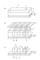
- FIG. 1(a) is a schematic perspective view for explaining the photosensitive layer forming step in the resist pattern forming step
- FIG. 1(b) is a schematic perspective view for explaining the exposure step in the resist pattern forming step
- 1(c) is a schematic perspective view for explaining the developing step in the resist pattern forming step.
- FIGS. 2A, 2B, and 2C are schematic perspective views for explaining the formation of a conductor pattern based on a defective resist pattern.
- FIG. 3 is a schematic perspective view for explaining the appearance inspection process.
- FIG. 4 is a schematic diagram for explaining light emission from the substrate.
- a or B may include either A or B, or both.
- a resist pattern inspection method includes an appearance inspection step of visually inspecting a resist pattern based on light emitted from a substrate on which a resist pattern is formed.
- the resist pattern inspection method may include a resist pattern forming step of forming a resist pattern on the substrate before the appearance inspection step.
- the resist pattern inspection method may include a luminescent material deposition step of depositing a luminescent material on the conductor surface of the substrate.
- the resist pattern inspection method may include other steps.
- the term "process” is used not only to refer to an independent process, but also to include a process in which the intended effect of the process is achieved even if the process cannot be clearly distinguished from other processes.
- the resist pattern can be said to be a pattern of a photocured product of a photosensitive resin composition, or a relief pattern.
- the resist pattern forming process includes a photosensitive layer forming process in which a photosensitive layer is laminated on a substrate (see FIG. 1(a)), and a photocuring area in which a predetermined portion of the photosensitive layer is irradiated with actinic rays. (see FIG. 1(b)), and a developing step (see FIG. 1(c)) to remove a region other than a predetermined portion of the photosensitive layer from the substrate.
- the resist pattern forming step may include other steps as necessary.
- a photosensitive layer 2 and a support 3 are formed on a substrate 1.
- the substrate 1 includes, for example, an insulating layer 1a and a conductor layer 1b formed on the insulating layer 1a.
- the photosensitive layer 2 is formed on the conductor layer 1b of the substrate 1.
- the conductor layer 1b is, for example, electroless copper plating.
- the photosensitive layer 2 is a layer formed using a photosensitive resin composition whose properties change (for example, photocures) when irradiated with light.
- the photosensitive resin composition forming the photosensitive layer 2 contains, for example, a binder polymer, a photopolymerizable compound, and a photopolymerization initiator.
- the photosensitive resin composition forming the photosensitive layer 2 may contain a photosensitizer, a polymerization inhibitor, or other components as necessary.
- the photosensitive resin composition forming the photosensitive layer 2 includes, for example, dyes such as malachite green, Victoria pure blue, brilliant green, and methyl violet, tribromophenyl sulfone, leuco crystal violet, diphenylamine, benzylamine, triphenylamine, and diethyl.
- Photocoloring agents such as aniline and o-chloroaniline, thermal coloration inhibitors, plasticizers such as p-toluenesulfonamide, pigments, fillers, antifoaming agents, flame retardants, adhesion agents, leveling agents, peeling accelerators , antioxidants, fragrances, imaging agents, thermal crosslinking agents, and other additives.
- a polymer film (support film) having heat resistance and solvent resistance such as polyester such as polyethylene terephthalate (PET), polyolefin such as polypropylene, and polyethylene, may be used.
- the photosensitive element includes, for example, a support, a photosensitive layer, and a protective layer in this order. After removing the protective layer, the photosensitive layer of the photosensitive element is pressed onto the substrate 1 while being heated, thereby forming the photosensitive layer 2 and the support 3 on the substrate 1. As a result, a laminate 4 including the substrate 1, the photosensitive layer 2, the support 3, and the support film (not shown) in this order is obtained. Note that an intermediate layer or the like may be arranged between the support 3 and the photosensitive layer 2.
- the photosensitive layer 2 is exposed to actinic light through the support 3.
- the exposed area irradiated with the actinic light is photocured, and a photocured area 2a (latent image) is formed.
- a known exposure method can be applied, such as a method of irradiating actinic rays imagewise through a photomask 5 called artwork (mask exposure method), an LDI (Laser Direct Imaging) exposure method, or , a method of irradiating image-wise through a lens using actinic light onto which an image of a photomask is projected (projection exposure method), and the like.
- the uncured portion 2b of the photosensitive layer 2 is removed from the substrate 1.
- a resist pattern 6 consisting of a photocured portion 2a obtained by photocuring the photosensitive layer 2 is formed on the substrate 1.
- a region 1c where the resist pattern 6 is not formed and a region 1d on the conductor surface of the substrate 1 where the resist pattern 6 is formed are formed.
- Region 1c is also a region not covered with resist pattern 6 on the surface of conductor layer 1b.
- the region 1d is also a region covered by the resist pattern 6 on the surface of the conductor layer 1b.
- the thickness of the resist pattern 6 formed on the substrate 1 may be, for example, 0.05 ⁇ m or more, 0.1 ⁇ m or more, 1 ⁇ m or more, or 5 ⁇ m or more. Further, the thickness of the resist pattern 6 formed on the substrate 1 may be, for example, 500 ⁇ m or less, 300 ⁇ m or less, 100 ⁇ m or less, or 60 ⁇ m or less. The minimum value and maximum value of the thickness of these resist patterns 6 can be appropriately combined.
- the thickness of the resist pattern 6 formed on the substrate 1 may be 0.05 ⁇ m or more and 500 ⁇ m or less, 0.1 ⁇ m or more and 300 ⁇ m or less, 1 ⁇ m or more and 100 ⁇ m or less, or 5 ⁇ m or more and 60 ⁇ m or less.
- the thickness of the resist pattern 6 is the height relative to the substrate 1 in the direction perpendicular to the main surface of the substrate 1.
- the resist pattern 6 formed on the substrate 1 has, for example, luminescent properties.
- Light emission is also called luminescence (cold light), and refers to, for example, when a device is irradiated with excitation light such as inspection light, it absorbs the excitation light and emits light. Furthermore, light emission refers to light emitted in this manner.
- the light emission includes fluorescence, phosphorescence, and the like. Fluorescence is light emission that stops immediately when the excitation light irradiation is stopped. Phosphorescence is light emission that continues even after the irradiation of light such as inspection light is stopped. Having luminescent property means having such a property of emitting light, that is, having a property of emitting light by absorbing the excitation light when irradiated with the excitation light. Note that the resist pattern 6 does not need to have luminescence.
- a luminescent material is deposited on the conductor surface of the substrate 1 in order to increase the luminescence intensity of the substrate 1.
- the conductor surface of the substrate 1 is, for example, the surface of the conductor layer 1b opposite to the insulating layer 1a, and the surface of the conductor layer 1b on the side on which the resist pattern 6 is formed. Therefore, in the luminescent material attachment step, the luminescent material is deposited on the surface of the conductor layer 1b of the substrate 1.
- a luminescent material is a material that emits light when irradiated with excitation light. If the luminescent material is a fluorescent material, this emission will be fluorescence.
- the luminescent material is a phosphorescent material
- this emission will be phosphorescent.
- a luminescent material fluorescent material or phosphorescent material
- a luminescent dye fluorescent dye or phosphorescent dye
- the luminescent dye for example, xanthene dyes, coumarin dyes, pyrazoline dyes, dipyrromethene dipromethene dyes, anthracene dyes, pyrene dyes, perylene dyes, lophine dyes (also referred to as lophines, lophine compounds, etc.), etc. may be used.
- the luminescent material for example, a fluorescent stain containing a luminescent dye may be used.
- the luminescent material attachment step can be performed, for example, at any timing before the resist pattern forming step, during the resist pattern forming step, or after the resist pattern forming step.
- the substrate 1 can be immersed in a fluorescent dye solution as a luminescent material.
- fluorescent staining solution include saturated solutions of xanthene dyes, coumarin dyes, pyrazoline dyes, dipyrromethene dipromethene dyes, anthracene dyes, pyrene dyes, perylene dyes, and lophine dyes, and mixed solutions thereof.
- the above dyes contain, for example, imidazole, pyridine, oxazole, pyrazole, thiazole, triazine, triazole, benzotriazole, 5-carboxybenzotriazole, tetrazole, 5-aminotetrazole, thiol, thiophene, benzoxazolylthiophene as a substituent. You may do so.
- substituents may be used alone or in combination of two or more. For example, a saturated aqueous solution of Rhodamine B (Fuji Film Wako Pure Chemical Industries, Ltd.), which is a xanthene dye, is used.
- the solvent examples include water, methanol, ethanol, acetone, methyl ethyl ketone, methyl cellosolve, ethyl cellosolve, toluene, N,N-dimethylformamide, propylene glycol monomethyl ether, and mixed solvents thereof.
- the entire substrate 1 may be immersed in the fluorescent dyeing solution, or a portion of the substrate 1 may be immersed in the fluorescent dyeing solution so that the entire substrate 1 is immersed in the fluorescent dyeing solution.
- a fluorescent dyeing liquid may be dropped onto the substrate 1 on which the resist pattern 6 is formed.
- the fluorescent dyeing liquid may be dropped on the entire substrate 1, or the fluorescent dyeing liquid may be dropped on a part of the substrate 1 on which the resist pattern 6 is formed so that the fluorescent dyeing liquid is dropped on the entire substrate 1. Good too.
- the luminescent material may be added to the developer and rinse solution for removing the uncured portion 2b of the photosensitive layer 2 from the substrate 1. After the fluorescent dye is deposited on the conductor surface of the substrate 1, the fluorescent dye liquid is removed from areas other than the conductor surface of the substrate 1.
- the conductive surface of the substrate 1 may be sufficiently washed with water and then air blow-dried.
- the conductor surface of the substrate 1 may be treated with a rust preventive agent before the substrate 1 is immersed in a fluorescent dye solution as a luminescent material. That is, a rust preventive agent adhesion step for adhering a rust preventive agent to the conductor surface of the substrate 1 may be performed before the light emitting material adhesion step.
- rust preventives include imidazole, imidazole derivatives, pyridine, pyridine derivatives, oxazole, oxazole derivatives, pyrazole, pyrazole derivatives, thiazole, thiazole derivatives, triazine, triazine derivatives, triazole, triazole derivatives, benzotriazole, benzotriazole derivatives, 5-carboxybenzotriazole, 5-carboxybenzotriazole derivative, tetrazole, tetrazole derivative, 5-aminotetrazole, 5-aminotetrazole derivative, thiol, thiol derivative, thiophene, thiophene derivative, benzoxazolylthiophene, benzoxazoli
- examples include ruthiophene derivatives.
- the rust inhibitor may be diluted with a solvent.
- rust preventives may be used alone or in combination of two or more.
- the solvent include water, methanol, ethanol, acetone, methyl ethyl ketone, methyl cellosolve, ethyl cellosolve, toluene, N,N-dimethylformamide, propylene glycol monomethyl ether, and mixed solvents thereof.
- the entire substrate 1 may be immersed in the rust preventive agent, or a portion of the substrate 1 may be immersed in the rust preventive agent such that the entire substrate 1 is immersed in the rust preventive agent.
- a rust preventive agent may be dropped onto the substrate 1 on which the resist pattern 6 is formed.
- the rust preventive agent may be dripped onto the entire substrate 1, or the rust preventive agent may be dripped onto a portion of the substrate 1 on which the resist pattern 6 is formed so that the rust preventive agent is dripped onto the entire substrate 1.
- a rust preventive agent may be added to the developer and rinse solution for removing the uncured portion 2b of the photosensitive layer 2 from the substrate 1 in the developing step in the resist pattern forming step.
- the rust preventive agent is removed from areas other than the substrate 1.
- the conductor surface may be thoroughly washed with water and air blow dried.
- the luminescent material and the rust preventive agent may be mixed, and the treatment of the conductor surface of the substrate 1 with the rust preventive agent and the treatment of the conductor surface of the substrate 1 with the luminescent material may be performed simultaneously. That is, the luminescent material attachment step and the rust preventive agent attachment step may be performed together. Either the conductor surface of the substrate 1 may be treated with a rust preventive agent or the conductor surface of the substrate 1 may be treated with a luminescent material.
- ⁇ Appearance inspection process the appearance of the resist pattern 6 is inspected based on light emission (fluorescence or phosphorescence) from the substrate 1 on which the resist pattern 6 is formed. That is, in the appearance inspection process, the appearance of the resist pattern 6 is inspected based on the light emitted from the substrate 1.
- the resist pattern 6 is visually inspected in order to find defects before forming the conductor pattern.
- the outline of the resist pattern 6 is detected based on light emitted from the substrate 1, and the appearance of the resist pattern 6 is inspected based on the detected outline.
- inspection light as excitation light is emitted onto the substrate 1 on which the resist pattern 6 is formed, and light emitted from the substrate 1 is received. That is, the light emitted from the substrate 1 is received.
- the wavelength of the inspection light may be, for example, 390 nm or less, 380 nm or less, or 370 nm or less. Further, the wavelength of the inspection light may be, for example, 190 nm or more, 250 nm or more, or 300 nm or more. The minimum value and maximum value of these wavelengths can be combined as appropriate.
- the wavelength of the inspection light may be 390 nm or less and 190 nm or more, 380 nm or more and 250 nm or more, or 370 nm or more and 300 nm or more.
- the light sources for the inspection light include carbon arc lamps, mercury vapor arc lamps, high-pressure mercury lamps, ultra-high-pressure mercury lamps, xenon lamps, gas lasers such as argon lasers, solid-state lasers such as YAG lasers, semiconductor lasers, LEDs, and other light sources. etc., and only the light having the wavelength of the above inspection light can be used by using an optical filter.
- the wavelength range in which luminescence is sensed can be changed arbitrarily, and may be, for example, visible light from 400 nm to 800 nm.
- the wavelength range for light emission sensing may be blue light of 400 nm to 500 nm, green light of 500 nm to 600 nm, or red light of 600 nm to 800 nm, and one wavelength range can be used alone or two or more wavelength ranges can be used in combination.
- the light-receiving area of the substrate 1 that receives light emission in the visual inspection process may be, for example, 1 cm 2 or more and 2500 cm 2 or less, 5 cm 2 or more and 1200 cm 2 or less, or 25 cm 2 or more and 600 cm 2 or less.
- the outline 10 of the resist pattern 6 is specified based on the contrast between the light emission and the light emission. For example, in a received light image of emitted light, a boundary where contrast such as brightness or chromaticity increases is detected. Then, this detected boundary is specified as the outline 10 of the resist pattern 6.
- an automatic optical visual inspection device such as AOI Orbotech Ultra Dimension 800 (manufactured by Nippon Orbotech Co., Ltd., trade name) is used, for example.
- the appearance inspection of the resist pattern 6 includes, for example, an inspection to check the presence or absence of a defect 8 in the resist pattern 6, an inspection to check the shape, position, size, etc. (hereinafter also referred to as "shape etc.") of the defect 8 in the resist pattern 6, Examples include an inspection that examines the shape of the resist pattern 6 or an inspection that measures the line width of the resist pattern 6.
- the outline 10 of the resist pattern 6 detected based on the light emission from the substrate 1 and the resist 6 will be compared with pattern data 11 for forming pattern data 11.
- pattern data 11 for example, CAD data of the resist pattern 6 is used.
- a portion 10a where the detected contour 10 differs from the pattern data 11 is detected as a defect 8 in the resist pattern 6.
- the number of detected defects 8 is calculated.
- the outline 10 of the resist pattern 6 detected based on the light emitted from the substrate 1 and the The pattern data 11 for forming pattern 6 will be compared. Then, a portion 10a where the detected contour 10 differs from the pattern data 11 is detected as a defect 8 in the resist pattern 6. Then, based on the outline of the detected defect 8, the shape etc. of the detected defect 8 is investigated.
- the contour 10 of the resist pattern 6 detected based on the light emitted from the substrate 1 and the shape of the resist pattern 6 formed in the resist pattern forming process are used.
- the line width of the resist pattern 6 is measured by measuring the interval between the contours 10 of the resist pattern 6 detected based on light emission from the substrate 1.
- the resist pattern manufacturing method includes a resist pattern forming step of forming a resist pattern 6 on the substrate 1, and a luminescent material attachment step of depositing a luminescent material on the conductor surface of the substrate 1.
- the resist pattern forming step of the resist pattern manufacturing method may be the same as the resist pattern forming step of the resist pattern inspection method described above.
- the luminescent material attaching step in the resist pattern manufacturing method may be, for example, the same as the luminescent material attaching step in the resist pattern inspection method described above.
- the resist pattern manufacturing method may include other steps.
- the substrate selection method includes an appearance inspection step of visually inspecting the resist pattern 6 based on light emitted from the substrate 1 on which the resist pattern 6 is formed, and a visual inspection step of visually inspecting the resist pattern 6 based on the appearance inspection in the appearance inspection step. and an evaluation step for evaluating.
- the appearance inspection step of the substrate selection method may be, for example, similar to the appearance inspection step of the resist pattern inspection method described above.
- a light-emitting material may be attached to the conductor surface of the substrate to be visually inspected in the visual inspection step of the substrate sorting method.
- the substrate sorting method may include other steps.
- the resist pattern 6 is evaluated based on predetermined criteria.
- the resist pattern 6 is evaluated based on the number of defects 8 in the resist pattern 6 in the evaluation process. For example, in the evaluation process, if the number of defects 8 in the resist pattern 6 is less than a predetermined reference number, it is evaluated as good, and if the number of defects 8 in the resist pattern 6 exceeds a predetermined reference number, it is evaluated as bad.
- the resist pattern 6 is evaluated based on the size of the defect 8 in the resist pattern 6 in the evaluation process. For example, in the evaluation process, if the shape of the defect 8 in the resist pattern 6 is within a predetermined tolerance range, it is evaluated as good, and if the shape of the defect 8 in the resist pattern 6 is outside the predetermined tolerance range, it is evaluated as poor. .
- the resist pattern 6 is evaluated based on the shape of the resist pattern 6 in the evaluation process. For example, in the evaluation step, if the degree of difference in shape of resist pattern 6 with respect to pattern data 11 is within a predetermined tolerance range, it is considered acceptable; If it is, it is considered defective.
- the resist pattern 6 is evaluated based on the line width of the resist pattern 6 in the evaluation process. For example, in the evaluation process, if the line width of the resist pattern 6 is within a predetermined reference range, it is evaluated as good, and if the line width of the resist pattern 6 is outside the predetermined reference range, it is evaluated as poor.
- the method for manufacturing a semiconductor package substrate or printed wiring board according to the present embodiment includes a conductor pattern forming step in which a conductor pattern is formed by etching or plating a substrate whose resist pattern evaluation in the above-described substrate selection method satisfies the criteria. Equipped with. That is, in the conductor pattern forming process, a conductor pattern is not formed by etching or plating on a substrate whose resist pattern evaluation in the substrate selection method does not meet the criteria.
- the method for manufacturing a semiconductor package substrate or a printed wiring board according to the present embodiment may include other steps such as a resist pattern removal step as necessary.
- the method for manufacturing a semiconductor package substrate or a printed wiring board is a method for manufacturing a semiconductor package substrate or a printed wiring board, and is a method for manufacturing a semiconductor package substrate or a method for manufacturing a printed wiring board.
- a semiconductor package substrate or a printed wiring board is manufactured by the manufacturing method.
- the conductor layer of the substrate that is not covered with the resist is etched away using a resist pattern formed on the substrate including the conductor layer as a mask. After the etching process, the resist is removed by removing the resist pattern 6 to form a conductor pattern.
- the plating process using a resist pattern 6 formed on the substrate 1 having the conductor layer 1b as a mask, copper or Plating solder, etc.
- the resist is removed by removing the resist pattern 6, and as shown in FIG. 6(c), the conductor layer 1b covered with this resist is etched. , a conductor pattern 9 is formed.
- the plating method may be electrolytic plating or electroless plating, and among these, electrolytic plating may be used.
- the resist pattern 6 is visually inspected based on the light emitted from the substrate 1 on which the resist pattern 6 is formed. Therefore, defects 8 in resist pattern 6 can be detected with high precision in a short time.
- the outline 10 of the resist pattern 6 detected based on the light emission from the substrate 1 on which the resist pattern 6 is formed is used to inspect the appearance of the resist pattern 6. 6 can be appropriately visually inspected.
- defects 8 of the resist pattern 6 are detected with high precision by comparing the detected outline 10 and pattern data 11 for forming the resist pattern 6 as an external appearance inspection of the resist pattern 6. can be detected.
- the formation state of the resist pattern 6 can be evaluated by measuring the line width of the resist pattern 6 based on the detected outline 10 as an appearance inspection of the resist pattern 6.
- this resist pattern inspection method by attaching a luminescent material onto the conductor surface of the substrate 1, the intensity of light emitted from the conductor surface of the substrate increases, so that the resist pattern 6 on the conductor surface of the substrate 1 is formed.
- the contrast between the light emitted from the region 1c which is not covered and the light emitted from the region 1d on the conductor surface of the substrate 1 where the resist pattern 6 is formed becomes large. Therefore, the accuracy of detecting the outline 10 of the resist pattern 6 based on the light emitted from the substrate 1 can be improved.
- the light emitted from the resist pattern 6 tends to become darker as the resist pattern 6 becomes thinner. Therefore, as the resist pattern 6 becomes thinner, the light emitted from the region 1c on the conductor surface of the substrate 1 where the resist pattern 6 is not formed and the light emission from the region 1d on the conductor surface of the substrate 1 where the resist pattern 6 is formed becomes different. The contrast between becomes greater. Therefore, from the viewpoint of increasing the contrast between the light emission from the region 1c on the conductor surface of the substrate 1 where the resist pattern 6 is not formed and the light emission from the region 1d on the conductor surface of the substrate 1 where the resist pattern 6 is formed.
- the thickness of the resist pattern 6 formed on the substrate 1 may be, for example, 500 ⁇ m or less, 300 ⁇ m or less, 100 ⁇ m or less, or 60 ⁇ m or less. Further, the thickness of the resist pattern 6 formed on the substrate 1 may be, for example, 0.05 ⁇ m or more, 0.1 ⁇ m or more, 1 ⁇ m or more, or 5 ⁇ m or more. The minimum value and maximum value of the thickness of these resist patterns 6 can be appropriately combined.
- the thickness of the resist pattern 6 formed on the substrate 1 may be 0.05 ⁇ m or more and 500 ⁇ m or less, 0.1 ⁇ m or more and 300 ⁇ m or less, 1 ⁇ m or more and 100 ⁇ m or less, or 5 ⁇ m or more and 60 ⁇ m or less.
- the resist pattern 6 is thick. between the light emission from the region 1c on the conductor surface of the substrate 1 where the resist pattern 6 is not formed and the light emission from the region 1d on the conductor surface of the substrate 1 where the resist pattern 6 is formed, while suppressing excessive The contrast can be increased. Therefore, the accuracy of detecting the outline 10 of the resist pattern 6 based on the light emitted from the substrate 1 can be improved.
- the resist pattern manufacturing method by attaching a luminescent material onto the conductor surface of the substrate 1, light emission from the region 1c on the conductor surface of the substrate 1 where the resist pattern 6 is not formed and The contrast between the light emitted from the region 1d on the conductor surface where the resist pattern 6 is formed becomes large. Therefore, for example, when detecting the outline 10 of the resist pattern 6 based on the light emitted from the substrate 1 on which the resist pattern 6 is formed, detection accuracy can be improved. Further, when measuring the line width of the resist pattern 6, etc., it becomes easier to focus on the surface of the resist pattern 6 or the outline of the resist pattern 6.
- the resist pattern 6 is formed by forming a resist pattern 6 having a thickness of 0.05 ⁇ m or more and 500 ⁇ m or less, 0.1 ⁇ m or more and 300 ⁇ m or less, 1 ⁇ m or more and 100 ⁇ m or less, or 5 ⁇ m or more and 60 ⁇ m or less. While suppressing that the resist pattern 6 becomes too thick, the light emission from the region 1c on the conductor surface of the substrate 1 where the resist pattern 6 is not formed and the light emission from the region 1d on the conductor surface of the substrate 1 where the resist pattern 6 is formed. The contrast between can be increased. Therefore, for example, the accuracy of detecting the outline 10 of the resist pattern 6 based on the light emitted from the substrate 1 can be improved.
- the resist pattern 6 is evaluated by the visual inspection of the resist pattern 6 based on the light emitted from the substrate 1. Therefore, compared to the visual inspection using an SEM, the substrate selection method can be performed in a short time and with high precision. can be sorted.
- the substrate 1 can be appropriately evaluated by evaluating the substrate 1 based on the number or shape of defects in the resist pattern 6.
- the conductive pattern 9 is formed by etching or plating the substrate 1 whose evaluation of the resist pattern 6 in the substrate selection method described above satisfies the criteria. , the occurrence of defects such as disconnection or short-circuiting of the conductor pattern 9 can be suppressed.
- Photosensitive Element and Substrate In Examples 1 to 5 and Comparative Example 1, the photosensitive element and substrate shown in Table 1 and below were used. The last two digits of the trade name of the photosensitive element indicate the thickness of the photosensitive layer (unit: ⁇ m).
- Manufactured photosensitive element F-3 RY-5125 (manufactured by Showa Denko Materials Co., Ltd., product name, photosensitive layer composition is the same as (F-2)) with MKG (malachite green) removed and photopolymerized.
- Photosensitive element F-4 manufactured using 0.5 times the amount of initiator and 0.3 times the amount of sensitizer: FL-7225 (manufactured by Showa Denko Materials Co., Ltd., trade name) (Base material)
- S-1 Cu sputtered PET film (manufactured by Geomatec Co., Ltd., plate thickness: 125 ⁇ m, Ra ⁇ 50 nm)
- S-2 GL-102 (manufactured by Ajinomoto Fine Techno Co., Ltd., trade name, Ra: approximately 100 nm)
- S-3 MCL-E67 (manufactured by Showa Denko Materials Co., Ltd., product name, Ra: approximately 300 nm)
- Examples 1, 3 to 4, and Comparative Example 1 S-1, which had been stored under moisture-proof conditions, was used as a substrate having a copper layer as a conductive layer.
- a substrate having a copper layer as a conductive layer was pickled and washed with water, dried with an air stream, and then heated to 80°C. Thereafter, the substrates S-1, S-2, and S-3 were immersed in a saturated aqueous solution of 1H-benzotriazole-5-carboxylic acid (Fujifilm Wako Pure Chemical Industries, Ltd.) for 60 minutes at 23°C, and then washed with water.
- 1H-benzotriazole-5-carboxylic acid Flujifilm Wako Pure Chemical Industries, Ltd.
- Examples 1 to 5 and Comparative Example 1 After drying with air flow, the copper surfaces of substrates S-1, S-2, and S-3 were further immersed in a saturated aqueous solution of Rhodamine B (Fuji Film Wako Pure Chemical Industries, Ltd.) at 23°C for 10 minutes. A fluorescent dye was attached to the. After washing with water and drying with a stream of air, the substrate was heated to 80°C. Thereafter, in Examples 1 to 5 and Comparative Example 1, the photosensitive element was laminated on the surface of the copper layer of the substrate. The laminate was laminated using a heat roll at 110° C. with a pressure of 0.4 MPa and 1° C. while peeling off the protective layer of the photosensitive element so that the photosensitive layer of the photosensitive element was in contact with the surface of the copper layer of the substrate. The roll speed was 0.0 m/min. In this way, laminates of Examples 1 to 5 and Comparative Example 1 were obtained in which the substrate, photosensitive layer, and support were laminated in this order. The obtained laminate was used as
- the support After exposure, the support is peeled off to expose the photosensitive layer, and a 1% by mass aqueous sodium carbonate solution at 30°C is sprayed for a time twice as long as the shortest development time (the shortest time for removing the unexposed areas). A portion was removed (development processing).
- a developed substrate exposed using a resolution evaluation photomask is referred to as a resolution evaluation pattern substrate, and a developed developed substrate exposed using a pattern inspection photomask is referred to as an inspection pattern substrate.
- the resolution was evaluated based on the value of /space width.
- the exposure amount is set such that the line width of the resist pattern is 30.0 ⁇ m. The above predetermined amount of energy was used.
- a direct drawing exposure device manufactured by Nippon Orbotech Co., Ltd., product name: "Nuvogo Fine"
- the visual inspection time was evaluated, and for Examples 1 to 5, the pattern detection rate of defects in the resist pattern was also evaluated as inspection accuracy.
- the pattern detection rate (inspection accuracy) refers to the probability that the inspection device was able to identify the outline of the resist pattern and recognize the pattern when performing the visual inspection.
- the inspection device before performing the visual inspection, use the inspection device to set the appropriate gray level (threshold value for light and dark binary conversion) according to each of Examples 1 to 5, and once this setting is completed, it is OK. If the process is not completed and an error occurs, it is judged as NG.
- A is the case where it is OK every time
- B is a case where it is not OK every time but the probability of NG is low
- the probability of NG is high.
- the case was designated as C.
- less than 10 minutes/ cm2 was graded A
- 10 minutes/cm2 or more and less than 5000 minutes/ 100cm2 was graded B
- 5000 minutes/100cm2 or more was graded C.
- the pattern detection rate was high. From this result, it was confirmed that the outline of the resist pattern can be easily detected and the inspection accuracy is high in the visual inspection of the resist pattern performed based on the fluorescence from the substrate on which the resist pattern is formed.
Landscapes
- Engineering & Computer Science (AREA)
- Physics & Mathematics (AREA)
- Microelectronics & Electronic Packaging (AREA)
- Manufacturing & Machinery (AREA)
- General Physics & Mathematics (AREA)
- General Health & Medical Sciences (AREA)
- Biochemistry (AREA)
- Analytical Chemistry (AREA)
- Immunology (AREA)
- Pathology (AREA)
- Chemical & Material Sciences (AREA)
- Life Sciences & Earth Sciences (AREA)
- Health & Medical Sciences (AREA)
- Photosensitive Polymer And Photoresist Processing (AREA)
Abstract
Le procédé d'inspection de motif de réserve de l'invention comprend une étape d'inspection d'apparence pour inspecter l'apparence d'un motif de réserve sur la base de la lumière émise par un substrat sur lequel le motif de réserve est formé. Ce procédé de fabrication de motif de réserve comprend : une étape de formation de motif de réserve pour former un motif de réserve sur un substrat ; et une étape d'adhérence de matériau électroluminescent pour faire adhérer un matériau électroluminescent à une surface d'un conducteur du substrat. Ce procédé de sélection de substrat comprend : une étape d'inspection d'apparence pour inspecter l'apparence du motif de réserve sur la base de la lumière émise par le substrat sur lequel le motif de réserve est formé ; et une étape d'évaluation pour évaluer le motif de réserve sur la base de l'inspection d'aspect dans l'étape d'inspection d'apparence. Ce procédé de fabrication d'un substrat de boîtier de semi-conducteur ou de carte de circuit imprimé comprend une étape de formation de motif conducteur pour former un motif conducteur par gravure ou placage du substrat, le motif de réserve du substrat ayant été évalué dans le procédé de sélection de substrat comme satisfaisant une norme.
Applications Claiming Priority (2)
| Application Number | Priority Date | Filing Date | Title |
|---|---|---|---|
| JP2022-119526 | 2022-07-27 | ||
| JP2022119526 | 2022-07-27 |
Publications (1)
| Publication Number | Publication Date |
|---|---|
| WO2024024484A1 true WO2024024484A1 (fr) | 2024-02-01 |
Family
ID=89706233
Family Applications (1)
| Application Number | Title | Priority Date | Filing Date |
|---|---|---|---|
| PCT/JP2023/025480 WO2024024484A1 (fr) | 2022-07-27 | 2023-07-10 | Procédé d'inspection de motifs de réserve, procédé de fabrication de motifs de réserve, procédé de sélection de substrat et procédé de fabrication de substrat de boîtier semi-conducteur ou de carte de circuit imprimé |
Country Status (1)
| Country | Link |
|---|---|
| WO (1) | WO2024024484A1 (fr) |
Citations (7)
| Publication number | Priority date | Publication date | Assignee | Title |
|---|---|---|---|---|
| JPH0294491A (ja) * | 1988-09-29 | 1990-04-05 | Hitachi Chem Co Ltd | 印刷配線板用銅張積層板 |
| JPH04213372A (ja) * | 1990-08-17 | 1992-08-04 | Mitsubishi Rayon Co Ltd | 画像形成用樹脂組成物および蛍光検出方式自動外観検査方法 |
| JP2000193596A (ja) * | 1998-12-24 | 2000-07-14 | Toshiba Corp | 検査方法 |
| JP2003243290A (ja) * | 2002-02-15 | 2003-08-29 | Seiko Epson Corp | レジストパターンの欠陥検査方法及びその欠陥検査装置 |
| JP2004233054A (ja) * | 2003-01-28 | 2004-08-19 | Furoobell:Kk | 基板検査装置および方法 |
| JP2012233790A (ja) * | 2011-05-02 | 2012-11-29 | Mitsubishi Electric Corp | 光硬化性樹脂の検査装置および検査方法 |
| JP2014009969A (ja) * | 2012-06-27 | 2014-01-20 | Sumitomo Metal Mining Co Ltd | 画像処理装置、画像処理方法、及び露光パターン検査装置 |
-
2023
- 2023-07-10 WO PCT/JP2023/025480 patent/WO2024024484A1/fr unknown
Patent Citations (7)
| Publication number | Priority date | Publication date | Assignee | Title |
|---|---|---|---|---|
| JPH0294491A (ja) * | 1988-09-29 | 1990-04-05 | Hitachi Chem Co Ltd | 印刷配線板用銅張積層板 |
| JPH04213372A (ja) * | 1990-08-17 | 1992-08-04 | Mitsubishi Rayon Co Ltd | 画像形成用樹脂組成物および蛍光検出方式自動外観検査方法 |
| JP2000193596A (ja) * | 1998-12-24 | 2000-07-14 | Toshiba Corp | 検査方法 |
| JP2003243290A (ja) * | 2002-02-15 | 2003-08-29 | Seiko Epson Corp | レジストパターンの欠陥検査方法及びその欠陥検査装置 |
| JP2004233054A (ja) * | 2003-01-28 | 2004-08-19 | Furoobell:Kk | 基板検査装置および方法 |
| JP2012233790A (ja) * | 2011-05-02 | 2012-11-29 | Mitsubishi Electric Corp | 光硬化性樹脂の検査装置および検査方法 |
| JP2014009969A (ja) * | 2012-06-27 | 2014-01-20 | Sumitomo Metal Mining Co Ltd | 画像処理装置、画像処理方法、及び露光パターン検査装置 |
Similar Documents
| Publication | Publication Date | Title |
|---|---|---|
| JP2019109543A (ja) | レジストパターンの形成方法、プリント配線板の製造方法、投影露光用感光性樹脂組成物及び感光性エレメント | |
| TWI666513B (zh) | Photosensitive element | |
| TW201710796A (zh) | 感光性元件、阻障層形成用樹脂組成物、抗蝕劑圖案的形成方法及印刷配線板的製造方法 | |
| WO2017007001A1 (fr) | Élément photosensible, corps stratifié, procédé de formation de motif de réserve, et procédé de fabrication de carte de circuit imprimé | |
| US5763123A (en) | Method for producing thin-film substrate | |
| WO2024024484A1 (fr) | Procédé d'inspection de motifs de réserve, procédé de fabrication de motifs de réserve, procédé de sélection de substrat et procédé de fabrication de substrat de boîtier semi-conducteur ou de carte de circuit imprimé | |
| WO2024024483A1 (fr) | Procédé d'inspection de motif de produit de réserve, procédé de fabrication de motif de produit de réserve, procédé de sélection de substrat et procédé de fabrication pour substrat de boîtier de semi-conducteurs ou carte de circuit imprimé | |
| TW202412134A (zh) | 抗蝕劑圖案之檢查方法、抗蝕劑圖案之製造方法、基板篩選方法及半導體封裝基板或印刷配線板之製造方法 | |
| JP4924230B2 (ja) | 感光性樹脂組成物、これを用いた感光性エレメント、レジストパターンの形成方法及びプリント配線板の製造方法 | |
| WO2022157895A1 (fr) | Procédé d'inspection de motif de réserve, procédé de fabrication de motif de réserve, procédé de sélection de substrat et procédé de fabrication de carte de circuit imprimé | |
| TWI801580B (zh) | 感光性元件、抗蝕劑圖案的形成方法及印刷配線板的製造方法 | |
| WO2023162934A1 (fr) | Procédé d'inspection de motif, procédé de fabrication de motif de réserve, procédé de sélection de substrat cible et procédé de fabrication de substrat cible | |
| EP0469957B1 (fr) | Composition de résine pour la formation d'une image | |
| JP5323442B2 (ja) | パターン形成方法 | |
| WO2024075626A1 (fr) | Élément photosensible, procédé de formation de motif de résine photosensible et procédé de fabrication de carte de circuit imprimé | |
| WO2023050062A1 (fr) | Polymère, composition de résine photosensible, élément photosensible, procédé de formation d'un motif de réserve, et procédé de formation d'un motif de câblage | |
| WO2024009870A1 (fr) | Composition de résine photosensible, élément photosensible, procédé de formation de motif de réserve, et procédé de production de boîtier à semi-conducteur ou de carte de circuit imprimé | |
| WO2022102675A1 (fr) | Élément photosensible, procédé de production de produit durci, procédé de production de motif de produit durci, et procédé de production de carte de câblage | |
| US20090111062A1 (en) | Pattern Formation Method | |
| TW202206944A (zh) | 感光性元件、光阻圖案之形成方法及印刷配線板之製造方法 | |
| TW202409108A (zh) | 感光性樹脂組成物、感光性元件、抗蝕劑圖案之形成方法及半導體封裝基板或印刷配線板之製造方法 | |
| Remes et al. | Direct laser write-on exposure of thick film screens | |
| CN113176267A (zh) | 一种光罩强光检测工艺 | |
| CN113588679A (zh) | 检查褪膜不净的方法 | |
| KR930008129B1 (ko) | 포토 레지스트 조성물 |
Legal Events
| Date | Code | Title | Description |
|---|---|---|---|
| 121 | Ep: the epo has been informed by wipo that ep was designated in this application |
Ref document number: 23846215 Country of ref document: EP Kind code of ref document: A1 |