WO2024024484A1 - Resist pattern inspection method, resist pattern manufacturing method, substrate selection method, and manufacturing method for semiconductor package substrate or printed circuit board - Google Patents
Resist pattern inspection method, resist pattern manufacturing method, substrate selection method, and manufacturing method for semiconductor package substrate or printed circuit board Download PDFInfo
- Publication number
- WO2024024484A1 WO2024024484A1 PCT/JP2023/025480 JP2023025480W WO2024024484A1 WO 2024024484 A1 WO2024024484 A1 WO 2024024484A1 JP 2023025480 W JP2023025480 W JP 2023025480W WO 2024024484 A1 WO2024024484 A1 WO 2024024484A1
- Authority
- WO
- WIPO (PCT)
- Prior art keywords
- resist pattern
- substrate
- pattern
- manufacturing
- inspection
- Prior art date
Links
- 239000000758 substrate Substances 0.000 title claims abstract description 234
- 238000000034 method Methods 0.000 title claims abstract description 108
- 238000007689 inspection Methods 0.000 title claims abstract description 102
- 238000004519 manufacturing process Methods 0.000 title claims abstract description 40
- 238000010187 selection method Methods 0.000 title claims abstract description 24
- 239000004065 semiconductor Substances 0.000 title claims abstract description 23
- 239000004020 conductor Substances 0.000 claims abstract description 96
- 239000000463 material Substances 0.000 claims abstract description 52
- 238000011156 evaluation Methods 0.000 claims abstract description 22
- 238000007747 plating Methods 0.000 claims abstract description 15
- 238000005530 etching Methods 0.000 claims abstract description 11
- 230000007547 defect Effects 0.000 claims description 41
- 238000011179 visual inspection Methods 0.000 claims description 27
- 238000000151 deposition Methods 0.000 claims description 7
- 230000008021 deposition Effects 0.000 claims description 2
- 230000007261 regionalization Effects 0.000 abstract description 5
- 239000010410 layer Substances 0.000 description 64
- 239000003795 chemical substances by application Substances 0.000 description 22
- JEIPFZHSYJVQDO-UHFFFAOYSA-N iron(III) oxide Inorganic materials O=[Fe]O[Fe]=O JEIPFZHSYJVQDO-UHFFFAOYSA-N 0.000 description 22
- 230000003449 preventive effect Effects 0.000 description 21
- 239000000975 dye Substances 0.000 description 20
- 230000000052 comparative effect Effects 0.000 description 9
- 239000010949 copper Substances 0.000 description 9
- 239000007850 fluorescent dye Substances 0.000 description 9
- 239000000243 solution Substances 0.000 description 9
- RYGMFSIKBFXOCR-UHFFFAOYSA-N Copper Chemical compound [Cu] RYGMFSIKBFXOCR-UHFFFAOYSA-N 0.000 description 8
- 229910052802 copper Inorganic materials 0.000 description 8
- 238000004043 dyeing Methods 0.000 description 8
- 238000012854 evaluation process Methods 0.000 description 8
- 230000005284 excitation Effects 0.000 description 8
- XLYOFNOQVPJJNP-UHFFFAOYSA-N water Substances O XLYOFNOQVPJJNP-UHFFFAOYSA-N 0.000 description 7
- ZWEHNKRNPOVVGH-UHFFFAOYSA-N 2-Butanone Chemical compound CCC(C)=O ZWEHNKRNPOVVGH-UHFFFAOYSA-N 0.000 description 6
- CSCPPACGZOOCGX-UHFFFAOYSA-N Acetone Chemical compound CC(C)=O CSCPPACGZOOCGX-UHFFFAOYSA-N 0.000 description 6
- LFQSCWFLJHTTHZ-UHFFFAOYSA-N Ethanol Chemical compound CCO LFQSCWFLJHTTHZ-UHFFFAOYSA-N 0.000 description 6
- OKKJLVBELUTLKV-UHFFFAOYSA-N Methanol Chemical compound OC OKKJLVBELUTLKV-UHFFFAOYSA-N 0.000 description 6
- ZMXDDKWLCZADIW-UHFFFAOYSA-N N,N-Dimethylformamide Chemical compound CN(C)C=O ZMXDDKWLCZADIW-UHFFFAOYSA-N 0.000 description 6
- YXFVVABEGXRONW-UHFFFAOYSA-N Toluene Chemical compound CC1=CC=CC=C1 YXFVVABEGXRONW-UHFFFAOYSA-N 0.000 description 6
- 238000001514 detection method Methods 0.000 description 6
- 238000011161 development Methods 0.000 description 6
- 230000018109 developmental process Effects 0.000 description 6
- RAXXELZNTBOGNW-UHFFFAOYSA-N imidazole Natural products C1=CNC=N1 RAXXELZNTBOGNW-UHFFFAOYSA-N 0.000 description 6
- 239000007788 liquid Substances 0.000 description 6
- FDZZZRQASAIRJF-UHFFFAOYSA-M malachite green Chemical compound [Cl-].C1=CC(N(C)C)=CC=C1C(C=1C=CC=CC=1)=C1C=CC(=[N+](C)C)C=C1 FDZZZRQASAIRJF-UHFFFAOYSA-M 0.000 description 5
- 229940107698 malachite green Drugs 0.000 description 5
- -1 polyethylene terephthalate Polymers 0.000 description 5
- 239000011342 resin composition Substances 0.000 description 5
- GUOVBFFLXKJFEE-UHFFFAOYSA-N 2h-benzotriazole-5-carboxylic acid Chemical compound C1=C(C(=O)O)C=CC2=NNN=C21 GUOVBFFLXKJFEE-UHFFFAOYSA-N 0.000 description 4
- JUJWROOIHBZHMG-UHFFFAOYSA-N Pyridine Chemical compound C1=CC=NC=C1 JUJWROOIHBZHMG-UHFFFAOYSA-N 0.000 description 4
- YTPLMLYBLZKORZ-UHFFFAOYSA-N Thiophene Chemical compound C=1C=CSC=1 YTPLMLYBLZKORZ-UHFFFAOYSA-N 0.000 description 4
- MWPLVEDNUUSJAV-UHFFFAOYSA-N anthracene Chemical compound C1=CC=CC2=CC3=CC=CC=C3C=C21 MWPLVEDNUUSJAV-UHFFFAOYSA-N 0.000 description 4
- 230000015572 biosynthetic process Effects 0.000 description 4
- ZYGHJZDHTFUPRJ-UHFFFAOYSA-N coumarin Chemical compound C1=CC=C2OC(=O)C=CC2=C1 ZYGHJZDHTFUPRJ-UHFFFAOYSA-N 0.000 description 4
- 239000003999 initiator Substances 0.000 description 4
- 238000004020 luminiscence type Methods 0.000 description 4
- QSHDDOUJBYECFT-UHFFFAOYSA-N mercury Chemical compound [Hg] QSHDDOUJBYECFT-UHFFFAOYSA-N 0.000 description 4
- BBEAQIROQSPTKN-UHFFFAOYSA-N pyrene Chemical compound C1=CC=C2C=CC3=CC=CC4=CC=C1C2=C43 BBEAQIROQSPTKN-UHFFFAOYSA-N 0.000 description 4
- 239000002904 solvent Substances 0.000 description 4
- RNIPJYFZGXJSDD-UHFFFAOYSA-N 2,4,5-triphenyl-1h-imidazole Chemical compound C1=CC=CC=C1C1=NC(C=2C=CC=CC=2)=C(C=2C=CC=CC=2)N1 RNIPJYFZGXJSDD-UHFFFAOYSA-N 0.000 description 3
- ULRPISSMEBPJLN-UHFFFAOYSA-N 2h-tetrazol-5-amine Chemical compound NC1=NN=NN1 ULRPISSMEBPJLN-UHFFFAOYSA-N 0.000 description 3
- 239000007864 aqueous solution Substances 0.000 description 3
- 239000003112 inhibitor Substances 0.000 description 3
- 230000001678 irradiating effect Effects 0.000 description 3
- 229910052753 mercury Inorganic materials 0.000 description 3
- 238000012545 processing Methods 0.000 description 3
- 239000011241 protective layer Substances 0.000 description 3
- 229920006395 saturated elastomer Polymers 0.000 description 3
- 239000000126 substance Substances 0.000 description 3
- 150000003536 tetrazoles Chemical class 0.000 description 3
- 150000003573 thiols Chemical class 0.000 description 3
- 239000001018 xanthene dye Substances 0.000 description 3
- JYEUMXHLPRZUAT-UHFFFAOYSA-N 1,2,3-triazine Chemical compound C1=CN=NN=C1 JYEUMXHLPRZUAT-UHFFFAOYSA-N 0.000 description 2
- ARXJGSRGQADJSQ-UHFFFAOYSA-N 1-methoxypropan-2-ol Chemical compound COCC(C)O ARXJGSRGQADJSQ-UHFFFAOYSA-N 0.000 description 2
- XNWFRZJHXBZDAG-UHFFFAOYSA-N 2-METHOXYETHANOL Chemical compound COCCO XNWFRZJHXBZDAG-UHFFFAOYSA-N 0.000 description 2
- ZNQVEEAIQZEUHB-UHFFFAOYSA-N 2-ethoxyethanol Chemical compound CCOCCO ZNQVEEAIQZEUHB-UHFFFAOYSA-N 0.000 description 2
- LLJKRUUAVWXDEI-UHFFFAOYSA-N 2-thiophen-2-yl-1,3-benzoxazole Chemical compound C1=CSC(C=2OC3=CC=CC=C3N=2)=C1 LLJKRUUAVWXDEI-UHFFFAOYSA-N 0.000 description 2
- PAYRUJLWNCNPSJ-UHFFFAOYSA-N Aniline Chemical compound NC1=CC=CC=C1 PAYRUJLWNCNPSJ-UHFFFAOYSA-N 0.000 description 2
- XKRFYHLGVUSROY-UHFFFAOYSA-N Argon Chemical compound [Ar] XKRFYHLGVUSROY-UHFFFAOYSA-N 0.000 description 2
- ZCQWOFVYLHDMMC-UHFFFAOYSA-N Oxazole Chemical compound C1=COC=N1 ZCQWOFVYLHDMMC-UHFFFAOYSA-N 0.000 description 2
- WTKZEGDFNFYCGP-UHFFFAOYSA-N Pyrazole Chemical compound C=1C=NNC=1 WTKZEGDFNFYCGP-UHFFFAOYSA-N 0.000 description 2
- CDBYLPFSWZWCQE-UHFFFAOYSA-L Sodium Carbonate Chemical compound [Na+].[Na+].[O-]C([O-])=O CDBYLPFSWZWCQE-UHFFFAOYSA-L 0.000 description 2
- FZWLAAWBMGSTSO-UHFFFAOYSA-N Thiazole Chemical compound C1=CSC=N1 FZWLAAWBMGSTSO-UHFFFAOYSA-N 0.000 description 2
- 235000010724 Wisteria floribunda Nutrition 0.000 description 2
- QRUDEWIWKLJBPS-UHFFFAOYSA-N benzotriazole Chemical compound C1=CC=C2N[N][N]C2=C1 QRUDEWIWKLJBPS-UHFFFAOYSA-N 0.000 description 2
- 239000012964 benzotriazole Substances 0.000 description 2
- WGQKYBSKWIADBV-UHFFFAOYSA-N benzylamine Chemical compound NCC1=CC=CC=C1 WGQKYBSKWIADBV-UHFFFAOYSA-N 0.000 description 2
- 229960000956 coumarin Drugs 0.000 description 2
- 235000001671 coumarin Nutrition 0.000 description 2
- 230000002950 deficient Effects 0.000 description 2
- 238000010586 diagram Methods 0.000 description 2
- DMBHHRLKUKUOEG-UHFFFAOYSA-N diphenylamine Chemical compound C=1C=CC=CC=1NC1=CC=CC=C1 DMBHHRLKUKUOEG-UHFFFAOYSA-N 0.000 description 2
- OVTCUIZCVUGJHS-UHFFFAOYSA-N dipyrrin Chemical compound C=1C=CNC=1C=C1C=CC=N1 OVTCUIZCVUGJHS-UHFFFAOYSA-N 0.000 description 2
- 238000001035 drying Methods 0.000 description 2
- 238000009713 electroplating Methods 0.000 description 2
- GVEPBJHOBDJJJI-UHFFFAOYSA-N fluoranthrene Natural products C1=CC(C2=CC=CC=C22)=C3C2=CC=CC3=C1 GVEPBJHOBDJJJI-UHFFFAOYSA-N 0.000 description 2
- 230000001771 impaired effect Effects 0.000 description 2
- 239000012046 mixed solvent Substances 0.000 description 2
- 230000003287 optical effect Effects 0.000 description 2
- 125000002080 perylenyl group Chemical group C1(=CC=C2C=CC=C3C4=CC=CC5=CC=CC(C1=C23)=C45)* 0.000 description 2
- CSHWQDPOILHKBI-UHFFFAOYSA-N peryrene Natural products C1=CC(C2=CC=CC=3C2=C2C=CC=3)=C3C2=CC=CC3=C1 CSHWQDPOILHKBI-UHFFFAOYSA-N 0.000 description 2
- 238000000016 photochemical curing Methods 0.000 description 2
- 229920000139 polyethylene terephthalate Polymers 0.000 description 2
- 239000005020 polyethylene terephthalate Substances 0.000 description 2
- DNXIASIHZYFFRO-UHFFFAOYSA-N pyrazoline Chemical compound C1CN=NC1 DNXIASIHZYFFRO-UHFFFAOYSA-N 0.000 description 2
- UMJSCPRVCHMLSP-UHFFFAOYSA-N pyridine Natural products COC1=CC=CN=C1 UMJSCPRVCHMLSP-UHFFFAOYSA-N 0.000 description 2
- PYWVYCXTNDRMGF-UHFFFAOYSA-N rhodamine B Chemical compound [Cl-].C=12C=CC(=[N+](CC)CC)C=C2OC2=CC(N(CC)CC)=CC=C2C=1C1=CC=CC=C1C(O)=O PYWVYCXTNDRMGF-UHFFFAOYSA-N 0.000 description 2
- 229940043267 rhodamine b Drugs 0.000 description 2
- 125000001424 substituent group Chemical group 0.000 description 2
- 238000012360 testing method Methods 0.000 description 2
- 229930192474 thiophene Natural products 0.000 description 2
- 150000003852 triazoles Chemical class 0.000 description 2
- SCEFCWXRXJZWHE-UHFFFAOYSA-N 1,2,3-tribromo-4-(2,3,4-tribromophenyl)sulfonylbenzene Chemical compound BrC1=C(Br)C(Br)=CC=C1S(=O)(=O)C1=CC=C(Br)C(Br)=C1Br SCEFCWXRXJZWHE-UHFFFAOYSA-N 0.000 description 1
- AKCRQHGQIJBRMN-UHFFFAOYSA-N 2-chloroaniline Chemical compound NC1=CC=CC=C1Cl AKCRQHGQIJBRMN-UHFFFAOYSA-N 0.000 description 1
- 229920002799 BoPET Polymers 0.000 description 1
- OKTJSMMVPCPJKN-UHFFFAOYSA-N Carbon Chemical compound [C] OKTJSMMVPCPJKN-UHFFFAOYSA-N 0.000 description 1
- VYZAMTAEIAYCRO-UHFFFAOYSA-N Chromium Chemical compound [Cr] VYZAMTAEIAYCRO-UHFFFAOYSA-N 0.000 description 1
- OAZWDJGLIYNYMU-UHFFFAOYSA-N Leucocrystal Violet Chemical compound C1=CC(N(C)C)=CC=C1C(C=1C=CC(=CC=1)N(C)C)C1=CC=C(N(C)C)C=C1 OAZWDJGLIYNYMU-UHFFFAOYSA-N 0.000 description 1
- 239000004698 Polyethylene Substances 0.000 description 1
- 239000004743 Polypropylene Substances 0.000 description 1
- 239000000654 additive Substances 0.000 description 1
- 239000002518 antifoaming agent Substances 0.000 description 1
- 239000003963 antioxidant agent Substances 0.000 description 1
- 229910052786 argon Inorganic materials 0.000 description 1
- 150000001565 benzotriazoles Chemical class 0.000 description 1
- 239000011230 binding agent Substances 0.000 description 1
- 229960001506 brilliant green Drugs 0.000 description 1
- 229910052799 carbon Inorganic materials 0.000 description 1
- 238000006243 chemical reaction Methods 0.000 description 1
- 150000001875 compounds Chemical class 0.000 description 1
- 239000003431 cross linking reagent Substances 0.000 description 1
- ZXJXZNDDNMQXFV-UHFFFAOYSA-M crystal violet Chemical compound [Cl-].C1=CC(N(C)C)=CC=C1[C+](C=1C=CC(=CC=1)N(C)C)C1=CC=C(N(C)C)C=C1 ZXJXZNDDNMQXFV-UHFFFAOYSA-M 0.000 description 1
- 125000004177 diethyl group Chemical group [H]C([H])([H])C([H])([H])* 0.000 description 1
- 230000000694 effects Effects 0.000 description 1
- 238000007772 electroless plating Methods 0.000 description 1
- 238000005516 engineering process Methods 0.000 description 1
- 239000000945 filler Substances 0.000 description 1
- 239000003063 flame retardant Substances 0.000 description 1
- 239000003205 fragrance Substances 0.000 description 1
- 239000007789 gas Substances 0.000 description 1
- 239000011521 glass Substances 0.000 description 1
- 239000012216 imaging agent Substances 0.000 description 1
- 238000003384 imaging method Methods 0.000 description 1
- 150000002460 imidazoles Chemical class 0.000 description 1
- 229940079865 intestinal antiinfectives imidazole derivative Drugs 0.000 description 1
- RUAIJHHRCIHFEV-UHFFFAOYSA-N methyl 4-amino-5-chlorothiophene-2-carboxylate Chemical compound COC(=O)C1=CC(N)=C(Cl)S1 RUAIJHHRCIHFEV-UHFFFAOYSA-N 0.000 description 1
- 239000011259 mixed solution Substances 0.000 description 1
- 239000000203 mixture Substances 0.000 description 1
- 150000007978 oxazole derivatives Chemical class 0.000 description 1
- 239000003504 photosensitizing agent Substances 0.000 description 1
- 239000000049 pigment Substances 0.000 description 1
- 239000004014 plasticizer Substances 0.000 description 1
- 229920000728 polyester Polymers 0.000 description 1
- 229920000573 polyethylene Polymers 0.000 description 1
- 229920000642 polymer Polymers 0.000 description 1
- 229920006254 polymer film Polymers 0.000 description 1
- 238000006116 polymerization reaction Methods 0.000 description 1
- 229920000098 polyolefin Polymers 0.000 description 1
- 229920001155 polypropylene Polymers 0.000 description 1
- 238000002360 preparation method Methods 0.000 description 1
- 150000003217 pyrazoles Chemical class 0.000 description 1
- 150000003222 pyridines Chemical class 0.000 description 1
- 239000012047 saturated solution Substances 0.000 description 1
- 229910000029 sodium carbonate Inorganic materials 0.000 description 1
- 229910000679 solder Inorganic materials 0.000 description 1
- 229940042055 systemic antimycotics triazole derivative Drugs 0.000 description 1
- 150000007979 thiazole derivatives Chemical class 0.000 description 1
- 150000003577 thiophenes Chemical class 0.000 description 1
- LMYRWZFENFIFIT-UHFFFAOYSA-N toluene-4-sulfonamide Chemical compound CC1=CC=C(S(N)(=O)=O)C=C1 LMYRWZFENFIFIT-UHFFFAOYSA-N 0.000 description 1
- 150000003918 triazines Chemical class 0.000 description 1
- ODHXBMXNKOYIBV-UHFFFAOYSA-N triphenylamine Chemical compound C1=CC=CC=C1N(C=1C=CC=CC=1)C1=CC=CC=C1 ODHXBMXNKOYIBV-UHFFFAOYSA-N 0.000 description 1
- ROVRRJSRRSGUOL-UHFFFAOYSA-N victoria blue bo Chemical compound [Cl-].C12=CC=CC=C2C(NCC)=CC=C1C(C=1C=CC(=CC=1)N(CC)CC)=C1C=CC(=[N+](CC)CC)C=C1 ROVRRJSRRSGUOL-UHFFFAOYSA-N 0.000 description 1
- 238000005406 washing Methods 0.000 description 1
- 229910052724 xenon Inorganic materials 0.000 description 1
- FHNFHKCVQCLJFQ-UHFFFAOYSA-N xenon atom Chemical compound [Xe] FHNFHKCVQCLJFQ-UHFFFAOYSA-N 0.000 description 1
Images


Classifications
-
- G—PHYSICS
- G01—MEASURING; TESTING
- G01N—INVESTIGATING OR ANALYSING MATERIALS BY DETERMINING THEIR CHEMICAL OR PHYSICAL PROPERTIES
- G01N21/00—Investigating or analysing materials by the use of optical means, i.e. using sub-millimetre waves, infrared, visible or ultraviolet light
- G01N21/84—Systems specially adapted for particular applications
- G01N21/88—Investigating the presence of flaws or contamination
- G01N21/95—Investigating the presence of flaws or contamination characterised by the material or shape of the object to be examined
- G01N21/956—Inspecting patterns on the surface of objects
-
- G—PHYSICS
- G03—PHOTOGRAPHY; CINEMATOGRAPHY; ANALOGOUS TECHNIQUES USING WAVES OTHER THAN OPTICAL WAVES; ELECTROGRAPHY; HOLOGRAPHY
- G03F—PHOTOMECHANICAL PRODUCTION OF TEXTURED OR PATTERNED SURFACES, e.g. FOR PRINTING, FOR PROCESSING OF SEMICONDUCTOR DEVICES; MATERIALS THEREFOR; ORIGINALS THEREFOR; APPARATUS SPECIALLY ADAPTED THEREFOR
- G03F7/00—Photomechanical, e.g. photolithographic, production of textured or patterned surfaces, e.g. printing surfaces; Materials therefor, e.g. comprising photoresists; Apparatus specially adapted therefor
- G03F7/20—Exposure; Apparatus therefor
-
- H—ELECTRICITY
- H05—ELECTRIC TECHNIQUES NOT OTHERWISE PROVIDED FOR
- H05K—PRINTED CIRCUITS; CASINGS OR CONSTRUCTIONAL DETAILS OF ELECTRIC APPARATUS; MANUFACTURE OF ASSEMBLAGES OF ELECTRICAL COMPONENTS
- H05K3/00—Apparatus or processes for manufacturing printed circuits
-
- H—ELECTRICITY
- H05—ELECTRIC TECHNIQUES NOT OTHERWISE PROVIDED FOR
- H05K—PRINTED CIRCUITS; CASINGS OR CONSTRUCTIONAL DETAILS OF ELECTRIC APPARATUS; MANUFACTURE OF ASSEMBLAGES OF ELECTRICAL COMPONENTS
- H05K3/00—Apparatus or processes for manufacturing printed circuits
- H05K3/02—Apparatus or processes for manufacturing printed circuits in which the conductive material is applied to the surface of the insulating support and is thereafter removed from such areas of the surface which are not intended for current conducting or shielding
- H05K3/06—Apparatus or processes for manufacturing printed circuits in which the conductive material is applied to the surface of the insulating support and is thereafter removed from such areas of the surface which are not intended for current conducting or shielding the conductive material being removed chemically or electrolytically, e.g. by photo-etch process
-
- H—ELECTRICITY
- H05—ELECTRIC TECHNIQUES NOT OTHERWISE PROVIDED FOR
- H05K—PRINTED CIRCUITS; CASINGS OR CONSTRUCTIONAL DETAILS OF ELECTRIC APPARATUS; MANUFACTURE OF ASSEMBLAGES OF ELECTRICAL COMPONENTS
- H05K3/00—Apparatus or processes for manufacturing printed circuits
- H05K3/10—Apparatus or processes for manufacturing printed circuits in which conductive material is applied to the insulating support in such a manner as to form the desired conductive pattern
- H05K3/18—Apparatus or processes for manufacturing printed circuits in which conductive material is applied to the insulating support in such a manner as to form the desired conductive pattern using precipitation techniques to apply the conductive material
Definitions
- the present disclosure relates to a method for inspecting a resist pattern, a method for manufacturing a resist pattern, a method for selecting a substrate, and a method for manufacturing a semiconductor package substrate or a printed wiring board.
- a photosensitive layer is laminated on the substrate.
- predetermined portions of the photosensitive layer are irradiated with active light through a photomask to cure the exposed portions.
- a resist pattern is formed on the substrate by removing the unexposed portion of the photosensitive layer with a developer.
- the substrate on which the resist pattern has been formed is subjected to etching or plating to form a conductive pattern on the substrate, and finally the cured portion of the photosensitive layer (resist pattern) is removed from the substrate. Peel and remove.
- the present disclosure aims to provide a method for inspecting a resist pattern, a method for manufacturing a resist pattern, a method for selecting a substrate, and a method for manufacturing a semiconductor package substrate or a printed wiring board, which can evaluate a resist pattern with high precision in a short time. purpose.
- the resist pattern inspection method of the present disclosure includes an appearance inspection step of visually inspecting the resist pattern based on light emitted from a substrate on which the resist pattern is formed.
- This resist pattern inspection method visually inspects the resist pattern based on light emitted from the substrate on which the resist pattern is formed, so it can detect defects in the resist pattern in a shorter time and with higher precision than the visual inspection using an SEM. can be detected.
- the outline of the resist pattern is detected based on light emitted from the substrate, and the resist pattern is visually inspected based on the detected outline. good.
- the outline of the resist pattern detected based on light emitted from the substrate is used as the visual inspection of the resist pattern, so that the resist pattern can be appropriately visually inspected.
- the detected contour may be compared with pattern data for forming the resist pattern in the appearance inspection step.
- defects in the resist pattern can be detected with high precision by comparing the detected contour with pattern data for forming the resist pattern as an external appearance inspection of the resist pattern.
- the line width of the resist pattern may be measured based on the detected contour.
- the formation state of the resist pattern can be evaluated by measuring the line width of the resist pattern based on the detected outline as an appearance inspection of the resist pattern.
- the resist pattern forming step of forming a resist pattern on a substrate and attaching a luminescent material on the conductor surface of the substrate are performed.
- the method may further include a step of attaching a luminescent material.
- this resist pattern inspection method by attaching a luminescent material to the conductor surface of the substrate, the intensity of light emitted from the conductor surface of the substrate increases. The contrast between the light emission and the light emission from the region of the conductor surface of the substrate where the resist pattern is formed is increased. Therefore, the accuracy of detecting the outline of the resist pattern based on the light emitted from the substrate can be improved.
- a resist pattern having a thickness of 0.05 ⁇ m or more and 500 ⁇ m or less may be formed.
- this resist pattern inspection method by forming a resist pattern with a thickness of 0.05 ⁇ m or more and 500 ⁇ m or less, the resist pattern is prevented from becoming too thick, and the resist pattern on the conductor surface of the substrate is not formed. It is possible to increase the contrast between the light emitted from the region and the light emitted from the region on the conductor surface of the substrate where the resist pattern is formed. Therefore, the accuracy of detecting the outline of the resist pattern based on the light emitted from the substrate can be improved.
- the method for manufacturing a resist pattern according to the present disclosure includes a resist pattern forming step of forming a resist pattern on a substrate, and a luminescent material attachment step of depositing a luminescent material on the conductor surface of the substrate.
- this resist pattern manufacturing method by attaching a luminescent material onto the conductor surface of the substrate, the intensity of light emitted from the conductor surface of the substrate increases.
- the contrast between the light emission and the light emission from the region of the conductor surface of the substrate where the resist pattern is formed is increased. Therefore, for example, when detecting the outline of a resist pattern based on light emitted from a substrate on which a resist pattern is formed, detection accuracy can be improved.
- a resist pattern having a thickness of 0.05 ⁇ m or more and 500 ⁇ m or less may be formed.
- this resist pattern manufacturing method by forming a resist pattern with a thickness of 0.05 ⁇ m or more and 500 ⁇ m or less, the resist pattern is prevented from becoming too thick, and the resist pattern on the conductor surface of the substrate is not formed. It is possible to increase the contrast between the light emitted from the region and the light emitted from the region on the conductor surface of the substrate where the resist pattern is formed. Therefore, for example, the accuracy of detecting the outline of a resist pattern based on the light emitted from the substrate can be improved.
- the substrate selection method includes a visual inspection step in which the resist pattern is visually inspected based on light emitted from the substrate on which the resist pattern is formed, and a resist pattern is evaluated based on the visual inspection in the visual inspection step. and an evaluation step.
- the resist pattern is evaluated by visual inspection of the resist pattern based on the light emitted from the substrate, so the substrates can be sorted in a shorter time and with high precision compared to visual inspection using SEM.
- the resist pattern in the substrate selection method described in [9], in the evaluation step, may be evaluated based on the number or shape of defects in the resist pattern.
- the substrate in this substrate selection method, can be appropriately evaluated by evaluating the resist pattern based on the number or shape of defects in the resist pattern.
- a luminescent material may be attached to the conductor surface of the substrate to be visually inspected in the visual inspection step.
- a luminescent material is attached to the conductor surface of the board to be visually inspected in the visual inspection process, so light is emitted from the area where the resist pattern is not formed on the conductor surface of the board and The contrast between the light emitted from the region where the resist pattern is formed is increased. Therefore, the appearance inspection of the resist pattern can be performed with high precision.
- the method for manufacturing a semiconductor package substrate or printed wiring board according to the present disclosure includes etching a substrate whose resist pattern evaluation satisfies the criteria in the substrate selection method described in any one of [9] to [11].
- a conductor pattern forming step is provided in which a conductor pattern is formed by processing or plating.
- conductive patterns are formed by etching or plating the substrates that meet the evaluation criteria of the resist pattern in the above-mentioned substrate selection method. The occurrence of defects can be suppressed.
- a resist pattern can be evaluated with high accuracy in a short time.
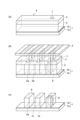
- FIG. 1(a) is a schematic perspective view for explaining the photosensitive layer forming step in the resist pattern forming step
- FIG. 1(b) is a schematic perspective view for explaining the exposure step in the resist pattern forming step
- 1(c) is a schematic perspective view for explaining the developing step in the resist pattern forming step.
- FIGS. 2A, 2B, and 2C are schematic perspective views for explaining the formation of a conductor pattern based on a defective resist pattern.
- FIG. 3 is a schematic perspective view for explaining the appearance inspection process.
- FIG. 4 is a schematic diagram for explaining light emission from the substrate.
- a or B may include either A or B, or both.
- a resist pattern inspection method includes an appearance inspection step of visually inspecting a resist pattern based on light emitted from a substrate on which a resist pattern is formed.
- the resist pattern inspection method may include a resist pattern forming step of forming a resist pattern on the substrate before the appearance inspection step.
- the resist pattern inspection method may include a luminescent material deposition step of depositing a luminescent material on the conductor surface of the substrate.
- the resist pattern inspection method may include other steps.
- the term "process” is used not only to refer to an independent process, but also to include a process in which the intended effect of the process is achieved even if the process cannot be clearly distinguished from other processes.
- the resist pattern can be said to be a pattern of a photocured product of a photosensitive resin composition, or a relief pattern.
- the resist pattern forming process includes a photosensitive layer forming process in which a photosensitive layer is laminated on a substrate (see FIG. 1(a)), and a photocuring area in which a predetermined portion of the photosensitive layer is irradiated with actinic rays. (see FIG. 1(b)), and a developing step (see FIG. 1(c)) to remove a region other than a predetermined portion of the photosensitive layer from the substrate.
- the resist pattern forming step may include other steps as necessary.
- a photosensitive layer 2 and a support 3 are formed on a substrate 1.
- the substrate 1 includes, for example, an insulating layer 1a and a conductor layer 1b formed on the insulating layer 1a.
- the photosensitive layer 2 is formed on the conductor layer 1b of the substrate 1.
- the conductor layer 1b is, for example, electroless copper plating.
- the photosensitive layer 2 is a layer formed using a photosensitive resin composition whose properties change (for example, photocures) when irradiated with light.
- the photosensitive resin composition forming the photosensitive layer 2 contains, for example, a binder polymer, a photopolymerizable compound, and a photopolymerization initiator.
- the photosensitive resin composition forming the photosensitive layer 2 may contain a photosensitizer, a polymerization inhibitor, or other components as necessary.
- the photosensitive resin composition forming the photosensitive layer 2 includes, for example, dyes such as malachite green, Victoria pure blue, brilliant green, and methyl violet, tribromophenyl sulfone, leuco crystal violet, diphenylamine, benzylamine, triphenylamine, and diethyl.
- Photocoloring agents such as aniline and o-chloroaniline, thermal coloration inhibitors, plasticizers such as p-toluenesulfonamide, pigments, fillers, antifoaming agents, flame retardants, adhesion agents, leveling agents, peeling accelerators , antioxidants, fragrances, imaging agents, thermal crosslinking agents, and other additives.
- a polymer film (support film) having heat resistance and solvent resistance such as polyester such as polyethylene terephthalate (PET), polyolefin such as polypropylene, and polyethylene, may be used.
- the photosensitive element includes, for example, a support, a photosensitive layer, and a protective layer in this order. After removing the protective layer, the photosensitive layer of the photosensitive element is pressed onto the substrate 1 while being heated, thereby forming the photosensitive layer 2 and the support 3 on the substrate 1. As a result, a laminate 4 including the substrate 1, the photosensitive layer 2, the support 3, and the support film (not shown) in this order is obtained. Note that an intermediate layer or the like may be arranged between the support 3 and the photosensitive layer 2.
- the photosensitive layer 2 is exposed to actinic light through the support 3.
- the exposed area irradiated with the actinic light is photocured, and a photocured area 2a (latent image) is formed.
- a known exposure method can be applied, such as a method of irradiating actinic rays imagewise through a photomask 5 called artwork (mask exposure method), an LDI (Laser Direct Imaging) exposure method, or , a method of irradiating image-wise through a lens using actinic light onto which an image of a photomask is projected (projection exposure method), and the like.
- the uncured portion 2b of the photosensitive layer 2 is removed from the substrate 1.
- a resist pattern 6 consisting of a photocured portion 2a obtained by photocuring the photosensitive layer 2 is formed on the substrate 1.
- a region 1c where the resist pattern 6 is not formed and a region 1d on the conductor surface of the substrate 1 where the resist pattern 6 is formed are formed.
- Region 1c is also a region not covered with resist pattern 6 on the surface of conductor layer 1b.
- the region 1d is also a region covered by the resist pattern 6 on the surface of the conductor layer 1b.
- the thickness of the resist pattern 6 formed on the substrate 1 may be, for example, 0.05 ⁇ m or more, 0.1 ⁇ m or more, 1 ⁇ m or more, or 5 ⁇ m or more. Further, the thickness of the resist pattern 6 formed on the substrate 1 may be, for example, 500 ⁇ m or less, 300 ⁇ m or less, 100 ⁇ m or less, or 60 ⁇ m or less. The minimum value and maximum value of the thickness of these resist patterns 6 can be appropriately combined.
- the thickness of the resist pattern 6 formed on the substrate 1 may be 0.05 ⁇ m or more and 500 ⁇ m or less, 0.1 ⁇ m or more and 300 ⁇ m or less, 1 ⁇ m or more and 100 ⁇ m or less, or 5 ⁇ m or more and 60 ⁇ m or less.
- the thickness of the resist pattern 6 is the height relative to the substrate 1 in the direction perpendicular to the main surface of the substrate 1.
- the resist pattern 6 formed on the substrate 1 has, for example, luminescent properties.
- Light emission is also called luminescence (cold light), and refers to, for example, when a device is irradiated with excitation light such as inspection light, it absorbs the excitation light and emits light. Furthermore, light emission refers to light emitted in this manner.
- the light emission includes fluorescence, phosphorescence, and the like. Fluorescence is light emission that stops immediately when the excitation light irradiation is stopped. Phosphorescence is light emission that continues even after the irradiation of light such as inspection light is stopped. Having luminescent property means having such a property of emitting light, that is, having a property of emitting light by absorbing the excitation light when irradiated with the excitation light. Note that the resist pattern 6 does not need to have luminescence.
- a luminescent material is deposited on the conductor surface of the substrate 1 in order to increase the luminescence intensity of the substrate 1.
- the conductor surface of the substrate 1 is, for example, the surface of the conductor layer 1b opposite to the insulating layer 1a, and the surface of the conductor layer 1b on the side on which the resist pattern 6 is formed. Therefore, in the luminescent material attachment step, the luminescent material is deposited on the surface of the conductor layer 1b of the substrate 1.
- a luminescent material is a material that emits light when irradiated with excitation light. If the luminescent material is a fluorescent material, this emission will be fluorescence.
- the luminescent material is a phosphorescent material
- this emission will be phosphorescent.
- a luminescent material fluorescent material or phosphorescent material
- a luminescent dye fluorescent dye or phosphorescent dye
- the luminescent dye for example, xanthene dyes, coumarin dyes, pyrazoline dyes, dipyrromethene dipromethene dyes, anthracene dyes, pyrene dyes, perylene dyes, lophine dyes (also referred to as lophines, lophine compounds, etc.), etc. may be used.
- the luminescent material for example, a fluorescent stain containing a luminescent dye may be used.
- the luminescent material attachment step can be performed, for example, at any timing before the resist pattern forming step, during the resist pattern forming step, or after the resist pattern forming step.
- the substrate 1 can be immersed in a fluorescent dye solution as a luminescent material.
- fluorescent staining solution include saturated solutions of xanthene dyes, coumarin dyes, pyrazoline dyes, dipyrromethene dipromethene dyes, anthracene dyes, pyrene dyes, perylene dyes, and lophine dyes, and mixed solutions thereof.
- the above dyes contain, for example, imidazole, pyridine, oxazole, pyrazole, thiazole, triazine, triazole, benzotriazole, 5-carboxybenzotriazole, tetrazole, 5-aminotetrazole, thiol, thiophene, benzoxazolylthiophene as a substituent. You may do so.
- substituents may be used alone or in combination of two or more. For example, a saturated aqueous solution of Rhodamine B (Fuji Film Wako Pure Chemical Industries, Ltd.), which is a xanthene dye, is used.
- the solvent examples include water, methanol, ethanol, acetone, methyl ethyl ketone, methyl cellosolve, ethyl cellosolve, toluene, N,N-dimethylformamide, propylene glycol monomethyl ether, and mixed solvents thereof.
- the entire substrate 1 may be immersed in the fluorescent dyeing solution, or a portion of the substrate 1 may be immersed in the fluorescent dyeing solution so that the entire substrate 1 is immersed in the fluorescent dyeing solution.
- a fluorescent dyeing liquid may be dropped onto the substrate 1 on which the resist pattern 6 is formed.
- the fluorescent dyeing liquid may be dropped on the entire substrate 1, or the fluorescent dyeing liquid may be dropped on a part of the substrate 1 on which the resist pattern 6 is formed so that the fluorescent dyeing liquid is dropped on the entire substrate 1. Good too.
- the luminescent material may be added to the developer and rinse solution for removing the uncured portion 2b of the photosensitive layer 2 from the substrate 1. After the fluorescent dye is deposited on the conductor surface of the substrate 1, the fluorescent dye liquid is removed from areas other than the conductor surface of the substrate 1.
- the conductive surface of the substrate 1 may be sufficiently washed with water and then air blow-dried.
- the conductor surface of the substrate 1 may be treated with a rust preventive agent before the substrate 1 is immersed in a fluorescent dye solution as a luminescent material. That is, a rust preventive agent adhesion step for adhering a rust preventive agent to the conductor surface of the substrate 1 may be performed before the light emitting material adhesion step.
- rust preventives include imidazole, imidazole derivatives, pyridine, pyridine derivatives, oxazole, oxazole derivatives, pyrazole, pyrazole derivatives, thiazole, thiazole derivatives, triazine, triazine derivatives, triazole, triazole derivatives, benzotriazole, benzotriazole derivatives, 5-carboxybenzotriazole, 5-carboxybenzotriazole derivative, tetrazole, tetrazole derivative, 5-aminotetrazole, 5-aminotetrazole derivative, thiol, thiol derivative, thiophene, thiophene derivative, benzoxazolylthiophene, benzoxazoli
- examples include ruthiophene derivatives.
- the rust inhibitor may be diluted with a solvent.
- rust preventives may be used alone or in combination of two or more.
- the solvent include water, methanol, ethanol, acetone, methyl ethyl ketone, methyl cellosolve, ethyl cellosolve, toluene, N,N-dimethylformamide, propylene glycol monomethyl ether, and mixed solvents thereof.
- the entire substrate 1 may be immersed in the rust preventive agent, or a portion of the substrate 1 may be immersed in the rust preventive agent such that the entire substrate 1 is immersed in the rust preventive agent.
- a rust preventive agent may be dropped onto the substrate 1 on which the resist pattern 6 is formed.
- the rust preventive agent may be dripped onto the entire substrate 1, or the rust preventive agent may be dripped onto a portion of the substrate 1 on which the resist pattern 6 is formed so that the rust preventive agent is dripped onto the entire substrate 1.
- a rust preventive agent may be added to the developer and rinse solution for removing the uncured portion 2b of the photosensitive layer 2 from the substrate 1 in the developing step in the resist pattern forming step.
- the rust preventive agent is removed from areas other than the substrate 1.
- the conductor surface may be thoroughly washed with water and air blow dried.
- the luminescent material and the rust preventive agent may be mixed, and the treatment of the conductor surface of the substrate 1 with the rust preventive agent and the treatment of the conductor surface of the substrate 1 with the luminescent material may be performed simultaneously. That is, the luminescent material attachment step and the rust preventive agent attachment step may be performed together. Either the conductor surface of the substrate 1 may be treated with a rust preventive agent or the conductor surface of the substrate 1 may be treated with a luminescent material.
- ⁇ Appearance inspection process the appearance of the resist pattern 6 is inspected based on light emission (fluorescence or phosphorescence) from the substrate 1 on which the resist pattern 6 is formed. That is, in the appearance inspection process, the appearance of the resist pattern 6 is inspected based on the light emitted from the substrate 1.
- the resist pattern 6 is visually inspected in order to find defects before forming the conductor pattern.
- the outline of the resist pattern 6 is detected based on light emitted from the substrate 1, and the appearance of the resist pattern 6 is inspected based on the detected outline.
- inspection light as excitation light is emitted onto the substrate 1 on which the resist pattern 6 is formed, and light emitted from the substrate 1 is received. That is, the light emitted from the substrate 1 is received.
- the wavelength of the inspection light may be, for example, 390 nm or less, 380 nm or less, or 370 nm or less. Further, the wavelength of the inspection light may be, for example, 190 nm or more, 250 nm or more, or 300 nm or more. The minimum value and maximum value of these wavelengths can be combined as appropriate.
- the wavelength of the inspection light may be 390 nm or less and 190 nm or more, 380 nm or more and 250 nm or more, or 370 nm or more and 300 nm or more.
- the light sources for the inspection light include carbon arc lamps, mercury vapor arc lamps, high-pressure mercury lamps, ultra-high-pressure mercury lamps, xenon lamps, gas lasers such as argon lasers, solid-state lasers such as YAG lasers, semiconductor lasers, LEDs, and other light sources. etc., and only the light having the wavelength of the above inspection light can be used by using an optical filter.
- the wavelength range in which luminescence is sensed can be changed arbitrarily, and may be, for example, visible light from 400 nm to 800 nm.
- the wavelength range for light emission sensing may be blue light of 400 nm to 500 nm, green light of 500 nm to 600 nm, or red light of 600 nm to 800 nm, and one wavelength range can be used alone or two or more wavelength ranges can be used in combination.
- the light-receiving area of the substrate 1 that receives light emission in the visual inspection process may be, for example, 1 cm 2 or more and 2500 cm 2 or less, 5 cm 2 or more and 1200 cm 2 or less, or 25 cm 2 or more and 600 cm 2 or less.
- the outline 10 of the resist pattern 6 is specified based on the contrast between the light emission and the light emission. For example, in a received light image of emitted light, a boundary where contrast such as brightness or chromaticity increases is detected. Then, this detected boundary is specified as the outline 10 of the resist pattern 6.
- an automatic optical visual inspection device such as AOI Orbotech Ultra Dimension 800 (manufactured by Nippon Orbotech Co., Ltd., trade name) is used, for example.
- the appearance inspection of the resist pattern 6 includes, for example, an inspection to check the presence or absence of a defect 8 in the resist pattern 6, an inspection to check the shape, position, size, etc. (hereinafter also referred to as "shape etc.") of the defect 8 in the resist pattern 6, Examples include an inspection that examines the shape of the resist pattern 6 or an inspection that measures the line width of the resist pattern 6.
- the outline 10 of the resist pattern 6 detected based on the light emission from the substrate 1 and the resist 6 will be compared with pattern data 11 for forming pattern data 11.
- pattern data 11 for example, CAD data of the resist pattern 6 is used.
- a portion 10a where the detected contour 10 differs from the pattern data 11 is detected as a defect 8 in the resist pattern 6.
- the number of detected defects 8 is calculated.
- the outline 10 of the resist pattern 6 detected based on the light emitted from the substrate 1 and the The pattern data 11 for forming pattern 6 will be compared. Then, a portion 10a where the detected contour 10 differs from the pattern data 11 is detected as a defect 8 in the resist pattern 6. Then, based on the outline of the detected defect 8, the shape etc. of the detected defect 8 is investigated.
- the contour 10 of the resist pattern 6 detected based on the light emitted from the substrate 1 and the shape of the resist pattern 6 formed in the resist pattern forming process are used.
- the line width of the resist pattern 6 is measured by measuring the interval between the contours 10 of the resist pattern 6 detected based on light emission from the substrate 1.
- the resist pattern manufacturing method includes a resist pattern forming step of forming a resist pattern 6 on the substrate 1, and a luminescent material attachment step of depositing a luminescent material on the conductor surface of the substrate 1.
- the resist pattern forming step of the resist pattern manufacturing method may be the same as the resist pattern forming step of the resist pattern inspection method described above.
- the luminescent material attaching step in the resist pattern manufacturing method may be, for example, the same as the luminescent material attaching step in the resist pattern inspection method described above.
- the resist pattern manufacturing method may include other steps.
- the substrate selection method includes an appearance inspection step of visually inspecting the resist pattern 6 based on light emitted from the substrate 1 on which the resist pattern 6 is formed, and a visual inspection step of visually inspecting the resist pattern 6 based on the appearance inspection in the appearance inspection step. and an evaluation step for evaluating.
- the appearance inspection step of the substrate selection method may be, for example, similar to the appearance inspection step of the resist pattern inspection method described above.
- a light-emitting material may be attached to the conductor surface of the substrate to be visually inspected in the visual inspection step of the substrate sorting method.
- the substrate sorting method may include other steps.
- the resist pattern 6 is evaluated based on predetermined criteria.
- the resist pattern 6 is evaluated based on the number of defects 8 in the resist pattern 6 in the evaluation process. For example, in the evaluation process, if the number of defects 8 in the resist pattern 6 is less than a predetermined reference number, it is evaluated as good, and if the number of defects 8 in the resist pattern 6 exceeds a predetermined reference number, it is evaluated as bad.
- the resist pattern 6 is evaluated based on the size of the defect 8 in the resist pattern 6 in the evaluation process. For example, in the evaluation process, if the shape of the defect 8 in the resist pattern 6 is within a predetermined tolerance range, it is evaluated as good, and if the shape of the defect 8 in the resist pattern 6 is outside the predetermined tolerance range, it is evaluated as poor. .
- the resist pattern 6 is evaluated based on the shape of the resist pattern 6 in the evaluation process. For example, in the evaluation step, if the degree of difference in shape of resist pattern 6 with respect to pattern data 11 is within a predetermined tolerance range, it is considered acceptable; If it is, it is considered defective.
- the resist pattern 6 is evaluated based on the line width of the resist pattern 6 in the evaluation process. For example, in the evaluation process, if the line width of the resist pattern 6 is within a predetermined reference range, it is evaluated as good, and if the line width of the resist pattern 6 is outside the predetermined reference range, it is evaluated as poor.
- the method for manufacturing a semiconductor package substrate or printed wiring board according to the present embodiment includes a conductor pattern forming step in which a conductor pattern is formed by etching or plating a substrate whose resist pattern evaluation in the above-described substrate selection method satisfies the criteria. Equipped with. That is, in the conductor pattern forming process, a conductor pattern is not formed by etching or plating on a substrate whose resist pattern evaluation in the substrate selection method does not meet the criteria.
- the method for manufacturing a semiconductor package substrate or a printed wiring board according to the present embodiment may include other steps such as a resist pattern removal step as necessary.
- the method for manufacturing a semiconductor package substrate or a printed wiring board is a method for manufacturing a semiconductor package substrate or a printed wiring board, and is a method for manufacturing a semiconductor package substrate or a method for manufacturing a printed wiring board.
- a semiconductor package substrate or a printed wiring board is manufactured by the manufacturing method.
- the conductor layer of the substrate that is not covered with the resist is etched away using a resist pattern formed on the substrate including the conductor layer as a mask. After the etching process, the resist is removed by removing the resist pattern 6 to form a conductor pattern.
- the plating process using a resist pattern 6 formed on the substrate 1 having the conductor layer 1b as a mask, copper or Plating solder, etc.
- the resist is removed by removing the resist pattern 6, and as shown in FIG. 6(c), the conductor layer 1b covered with this resist is etched. , a conductor pattern 9 is formed.
- the plating method may be electrolytic plating or electroless plating, and among these, electrolytic plating may be used.
- the resist pattern 6 is visually inspected based on the light emitted from the substrate 1 on which the resist pattern 6 is formed. Therefore, defects 8 in resist pattern 6 can be detected with high precision in a short time.
- the outline 10 of the resist pattern 6 detected based on the light emission from the substrate 1 on which the resist pattern 6 is formed is used to inspect the appearance of the resist pattern 6. 6 can be appropriately visually inspected.
- defects 8 of the resist pattern 6 are detected with high precision by comparing the detected outline 10 and pattern data 11 for forming the resist pattern 6 as an external appearance inspection of the resist pattern 6. can be detected.
- the formation state of the resist pattern 6 can be evaluated by measuring the line width of the resist pattern 6 based on the detected outline 10 as an appearance inspection of the resist pattern 6.
- this resist pattern inspection method by attaching a luminescent material onto the conductor surface of the substrate 1, the intensity of light emitted from the conductor surface of the substrate increases, so that the resist pattern 6 on the conductor surface of the substrate 1 is formed.
- the contrast between the light emitted from the region 1c which is not covered and the light emitted from the region 1d on the conductor surface of the substrate 1 where the resist pattern 6 is formed becomes large. Therefore, the accuracy of detecting the outline 10 of the resist pattern 6 based on the light emitted from the substrate 1 can be improved.
- the light emitted from the resist pattern 6 tends to become darker as the resist pattern 6 becomes thinner. Therefore, as the resist pattern 6 becomes thinner, the light emitted from the region 1c on the conductor surface of the substrate 1 where the resist pattern 6 is not formed and the light emission from the region 1d on the conductor surface of the substrate 1 where the resist pattern 6 is formed becomes different. The contrast between becomes greater. Therefore, from the viewpoint of increasing the contrast between the light emission from the region 1c on the conductor surface of the substrate 1 where the resist pattern 6 is not formed and the light emission from the region 1d on the conductor surface of the substrate 1 where the resist pattern 6 is formed.
- the thickness of the resist pattern 6 formed on the substrate 1 may be, for example, 500 ⁇ m or less, 300 ⁇ m or less, 100 ⁇ m or less, or 60 ⁇ m or less. Further, the thickness of the resist pattern 6 formed on the substrate 1 may be, for example, 0.05 ⁇ m or more, 0.1 ⁇ m or more, 1 ⁇ m or more, or 5 ⁇ m or more. The minimum value and maximum value of the thickness of these resist patterns 6 can be appropriately combined.
- the thickness of the resist pattern 6 formed on the substrate 1 may be 0.05 ⁇ m or more and 500 ⁇ m or less, 0.1 ⁇ m or more and 300 ⁇ m or less, 1 ⁇ m or more and 100 ⁇ m or less, or 5 ⁇ m or more and 60 ⁇ m or less.
- the resist pattern 6 is thick. between the light emission from the region 1c on the conductor surface of the substrate 1 where the resist pattern 6 is not formed and the light emission from the region 1d on the conductor surface of the substrate 1 where the resist pattern 6 is formed, while suppressing excessive The contrast can be increased. Therefore, the accuracy of detecting the outline 10 of the resist pattern 6 based on the light emitted from the substrate 1 can be improved.
- the resist pattern manufacturing method by attaching a luminescent material onto the conductor surface of the substrate 1, light emission from the region 1c on the conductor surface of the substrate 1 where the resist pattern 6 is not formed and The contrast between the light emitted from the region 1d on the conductor surface where the resist pattern 6 is formed becomes large. Therefore, for example, when detecting the outline 10 of the resist pattern 6 based on the light emitted from the substrate 1 on which the resist pattern 6 is formed, detection accuracy can be improved. Further, when measuring the line width of the resist pattern 6, etc., it becomes easier to focus on the surface of the resist pattern 6 or the outline of the resist pattern 6.
- the resist pattern 6 is formed by forming a resist pattern 6 having a thickness of 0.05 ⁇ m or more and 500 ⁇ m or less, 0.1 ⁇ m or more and 300 ⁇ m or less, 1 ⁇ m or more and 100 ⁇ m or less, or 5 ⁇ m or more and 60 ⁇ m or less. While suppressing that the resist pattern 6 becomes too thick, the light emission from the region 1c on the conductor surface of the substrate 1 where the resist pattern 6 is not formed and the light emission from the region 1d on the conductor surface of the substrate 1 where the resist pattern 6 is formed. The contrast between can be increased. Therefore, for example, the accuracy of detecting the outline 10 of the resist pattern 6 based on the light emitted from the substrate 1 can be improved.
- the resist pattern 6 is evaluated by the visual inspection of the resist pattern 6 based on the light emitted from the substrate 1. Therefore, compared to the visual inspection using an SEM, the substrate selection method can be performed in a short time and with high precision. can be sorted.
- the substrate 1 can be appropriately evaluated by evaluating the substrate 1 based on the number or shape of defects in the resist pattern 6.
- the conductive pattern 9 is formed by etching or plating the substrate 1 whose evaluation of the resist pattern 6 in the substrate selection method described above satisfies the criteria. , the occurrence of defects such as disconnection or short-circuiting of the conductor pattern 9 can be suppressed.
- Photosensitive Element and Substrate In Examples 1 to 5 and Comparative Example 1, the photosensitive element and substrate shown in Table 1 and below were used. The last two digits of the trade name of the photosensitive element indicate the thickness of the photosensitive layer (unit: ⁇ m).
- Manufactured photosensitive element F-3 RY-5125 (manufactured by Showa Denko Materials Co., Ltd., product name, photosensitive layer composition is the same as (F-2)) with MKG (malachite green) removed and photopolymerized.
- Photosensitive element F-4 manufactured using 0.5 times the amount of initiator and 0.3 times the amount of sensitizer: FL-7225 (manufactured by Showa Denko Materials Co., Ltd., trade name) (Base material)
- S-1 Cu sputtered PET film (manufactured by Geomatec Co., Ltd., plate thickness: 125 ⁇ m, Ra ⁇ 50 nm)
- S-2 GL-102 (manufactured by Ajinomoto Fine Techno Co., Ltd., trade name, Ra: approximately 100 nm)
- S-3 MCL-E67 (manufactured by Showa Denko Materials Co., Ltd., product name, Ra: approximately 300 nm)
- Examples 1, 3 to 4, and Comparative Example 1 S-1, which had been stored under moisture-proof conditions, was used as a substrate having a copper layer as a conductive layer.
- a substrate having a copper layer as a conductive layer was pickled and washed with water, dried with an air stream, and then heated to 80°C. Thereafter, the substrates S-1, S-2, and S-3 were immersed in a saturated aqueous solution of 1H-benzotriazole-5-carboxylic acid (Fujifilm Wako Pure Chemical Industries, Ltd.) for 60 minutes at 23°C, and then washed with water.
- 1H-benzotriazole-5-carboxylic acid Flujifilm Wako Pure Chemical Industries, Ltd.
- Examples 1 to 5 and Comparative Example 1 After drying with air flow, the copper surfaces of substrates S-1, S-2, and S-3 were further immersed in a saturated aqueous solution of Rhodamine B (Fuji Film Wako Pure Chemical Industries, Ltd.) at 23°C for 10 minutes. A fluorescent dye was attached to the. After washing with water and drying with a stream of air, the substrate was heated to 80°C. Thereafter, in Examples 1 to 5 and Comparative Example 1, the photosensitive element was laminated on the surface of the copper layer of the substrate. The laminate was laminated using a heat roll at 110° C. with a pressure of 0.4 MPa and 1° C. while peeling off the protective layer of the photosensitive element so that the photosensitive layer of the photosensitive element was in contact with the surface of the copper layer of the substrate. The roll speed was 0.0 m/min. In this way, laminates of Examples 1 to 5 and Comparative Example 1 were obtained in which the substrate, photosensitive layer, and support were laminated in this order. The obtained laminate was used as
- the support After exposure, the support is peeled off to expose the photosensitive layer, and a 1% by mass aqueous sodium carbonate solution at 30°C is sprayed for a time twice as long as the shortest development time (the shortest time for removing the unexposed areas). A portion was removed (development processing).
- a developed substrate exposed using a resolution evaluation photomask is referred to as a resolution evaluation pattern substrate, and a developed developed substrate exposed using a pattern inspection photomask is referred to as an inspection pattern substrate.
- the resolution was evaluated based on the value of /space width.
- the exposure amount is set such that the line width of the resist pattern is 30.0 ⁇ m. The above predetermined amount of energy was used.
- a direct drawing exposure device manufactured by Nippon Orbotech Co., Ltd., product name: "Nuvogo Fine"
- the visual inspection time was evaluated, and for Examples 1 to 5, the pattern detection rate of defects in the resist pattern was also evaluated as inspection accuracy.
- the pattern detection rate (inspection accuracy) refers to the probability that the inspection device was able to identify the outline of the resist pattern and recognize the pattern when performing the visual inspection.
- the inspection device before performing the visual inspection, use the inspection device to set the appropriate gray level (threshold value for light and dark binary conversion) according to each of Examples 1 to 5, and once this setting is completed, it is OK. If the process is not completed and an error occurs, it is judged as NG.
- A is the case where it is OK every time
- B is a case where it is not OK every time but the probability of NG is low
- the probability of NG is high.
- the case was designated as C.
- less than 10 minutes/ cm2 was graded A
- 10 minutes/cm2 or more and less than 5000 minutes/ 100cm2 was graded B
- 5000 minutes/100cm2 or more was graded C.
- the pattern detection rate was high. From this result, it was confirmed that the outline of the resist pattern can be easily detected and the inspection accuracy is high in the visual inspection of the resist pattern performed based on the fluorescence from the substrate on which the resist pattern is formed.
Abstract
This resist pattern inspection method comprises an appearance inspection step for inspecting the appearance of a resist pattern on the basis of light emitted from a substrate whereon the resist pattern is formed. This resist pattern manufacturing method comprises: a resist pattern formation step for forming a resist pattern on a substrate; and a light-emitting material adhering step for adhering a light-emitting material to a surface of a conductor of the substrate. This substrate selection method comprises: the appearance inspection step for inspecting the appearance of the resist pattern on the basis of the light emitted from the substrate whereon the resist pattern is formed; and an evaluation step for evaluating the resist pattern on the basis of the appearance inspection in the appearance inspection step. This manufacturing method for a semiconductor package substrate or a printed circuit board comprises a conductor pattern formation step for forming a conductor pattern by etching or plating the substrate, the resist pattern of the substrate having been evaluated in the substrate selection method as meeting a standard.
Description
本開示は、レジストパターンの検査方法、レジストパターンの製造方法、基板選別方法、及び、半導体パッケージ基板又はプリント配線板の製造方法に関する。
The present disclosure relates to a method for inspecting a resist pattern, a method for manufacturing a resist pattern, a method for selecting a substrate, and a method for manufacturing a semiconductor package substrate or a printed wiring board.
半導体パッケージ基板又はプリント配線板を製造する場合は、まず、基板上に感光層をラミネートする。次に、フォトマスクを通して感光層の所定部分に活性光線を照射して露光部を硬化させる。次に、支持体を剥離除去した後、感光層の未露光部を現像液で除去することにより、基板上にレジストパターンを形成する。次に、形成したレジストパターンをマスクとし、レジストパターンを形成した基板にエッチング処理又はめっき処理を施して基板上に導体パターンを形成し、最終的に感光層の硬化部分(レジストパターン)を基板から剥離除去する。
When manufacturing a semiconductor package substrate or printed wiring board, first, a photosensitive layer is laminated on the substrate. Next, predetermined portions of the photosensitive layer are irradiated with active light through a photomask to cure the exposed portions. Next, after peeling off the support, a resist pattern is formed on the substrate by removing the unexposed portion of the photosensitive layer with a developer. Next, using the formed resist pattern as a mask, the substrate on which the resist pattern has been formed is subjected to etching or plating to form a conductive pattern on the substrate, and finally the cured portion of the photosensitive layer (resist pattern) is removed from the substrate. Peel and remove.
このような、半導体パッケージ基板又はプリント配線板の製造工程において、フォトマスク又は感光層に付着した異物等により活性光線の露光障害が生じると、レジストパターンに欠陥が生じ、導体パターンに断線又はショート等の不良が生じ得る。そこで、従来は、導体パターンを外観検査することにより、導体パターンの断線又はショート等の不良を検査していた。
In the manufacturing process of semiconductor package substrates or printed wiring boards, if exposure to actinic rays is impaired due to foreign matter adhering to the photomask or photosensitive layer, defects may occur in the resist pattern, resulting in disconnections or short circuits in the conductor pattern. defects may occur. Therefore, conventionally, defects such as disconnections or short circuits in the conductor pattern have been inspected by visually inspecting the conductor pattern.
ところで、導体パターンを形成する前にレジストパターンを外観検査することで、半導体パッケージ基板又はプリント配線板の製造におけるより早い段階で不良を発見することができる。また、レジストパターン形成の歩留まりを評価することで、レジストパターン形成の改善につなげることができる。レジストパターンの外観検査は、従来、走査型電子顕微鏡(以下「SEM」ともいう)を用いて行われていた(例えば、特許文献1参照)。
Incidentally, by visually inspecting the resist pattern before forming the conductor pattern, defects can be discovered at an earlier stage in the manufacture of the semiconductor package substrate or printed wiring board. Furthermore, evaluating the yield of resist pattern formation can lead to improvements in resist pattern formation. Appearance inspection of resist patterns has conventionally been performed using a scanning electron microscope (hereinafter also referred to as "SEM") (see, for example, Patent Document 1).
しかしながら、SEMによる検査は、1mm2程度の極小範囲を検査するものである。このため、SEMを用いた、半導体パッケージ基板又はプリント配線板全体のレジストパターンの検査は、膨大な時間を要する。しかも、検査者及び検査に用いるSEMによって検査精度に大きなばらつきがある。
However, the inspection by SEM inspects a very small area of about 1 mm 2 . For this reason, it takes an enormous amount of time to inspect the resist pattern of the entire semiconductor package substrate or printed wiring board using the SEM. Furthermore, there are large variations in inspection accuracy depending on the inspector and the SEM used for the inspection.
そこで、本開示は、短時間で高精度にレジストパターンを評価できるレジストパターンの検査方法、レジストパターンの製造方法、基板選別方法、及び、半導体パッケージ基板又はプリント配線板の製造方法を提供することを目的とする。
Therefore, the present disclosure aims to provide a method for inspecting a resist pattern, a method for manufacturing a resist pattern, a method for selecting a substrate, and a method for manufacturing a semiconductor package substrate or a printed wiring board, which can evaluate a resist pattern with high precision in a short time. purpose.
[1] 本開示のレジストパターンの検査方法は、レジストパターンが形成された基板からの発光に基づいてレジストパターンを外観検査する外観検査工程を備える。
[1] The resist pattern inspection method of the present disclosure includes an appearance inspection step of visually inspecting the resist pattern based on light emitted from a substrate on which the resist pattern is formed.
このレジストパターンの検査方法では、レジストパターンが形成された基板からの発光に基づいてレジストパターンを外観検査するため、SEMを用いた外観検査に比べて、短時間で高精度にレジストパターンの欠陥を検出することができる。
This resist pattern inspection method visually inspects the resist pattern based on light emitted from the substrate on which the resist pattern is formed, so it can detect defects in the resist pattern in a shorter time and with higher precision than the visual inspection using an SEM. can be detected.
[2] [1]に記載のレジストパターンの検査方法において、外観検査工程では、基板からの発光に基づいてレジストパターンの輪郭を検出し、検出した輪郭に基づいてレジストパターンを外観検査してもよい。このレジストパターンの検査方法では、レジストパターンの外観検査として、基板からの発光に基づいて検出されるレジストパターンの輪郭を利用することで、レジストパターンを適切に外観検査することができる。
[2] In the resist pattern inspection method described in [1], in the visual inspection step, the outline of the resist pattern is detected based on light emitted from the substrate, and the resist pattern is visually inspected based on the detected outline. good. In this method for inspecting a resist pattern, the outline of the resist pattern detected based on light emitted from the substrate is used as the visual inspection of the resist pattern, so that the resist pattern can be appropriately visually inspected.
[3] [2]に記載のレジストパターンの検査方法において、外観検査工程では、検出した輪郭とレジストパターンを形成するためのパターンデータとを対比してもよい。このレジストパターンの検査方法では、レジストパターンの外観検査として、検出した輪郭とレジストパターンを形成するためのパターンデータとを対比することで、レジストパターンの欠陥を高精度に検出することができる。
[3] In the resist pattern inspection method described in [2], the detected contour may be compared with pattern data for forming the resist pattern in the appearance inspection step. In this resist pattern inspection method, defects in the resist pattern can be detected with high precision by comparing the detected contour with pattern data for forming the resist pattern as an external appearance inspection of the resist pattern.
[4] [2]に記載のレジストパターンの検査方法において、外観検査工程では、検出した輪郭に基づいてレジストパターンの線幅を計測してもよい。このレジストパターンの検査方法では、レジストパターンの外観検査として、検出した輪郭に基づいてレジストパターンの線幅を計測することで、レジストパターンの形成状態を評価することができる。
[4] In the resist pattern inspection method described in [2], in the appearance inspection step, the line width of the resist pattern may be measured based on the detected contour. In this resist pattern inspection method, the formation state of the resist pattern can be evaluated by measuring the line width of the resist pattern based on the detected outline as an appearance inspection of the resist pattern.
[5] [1]~[4]の何れか一つに記載のレジストパターンの検査方法において、基板上にレジストパターンを形成するレジストパターン形成工程と、基板の導体表面上に発光材料を付着させる発光材料付着工程と、を更に備えてもよい。このレジストパターンの検査方法では、基板の導体表面上に発光材料を付着させることで、基板の導体表面からの発光強度が増大するため、基板の導体表面のレジストパターンが形成されていない領域からの発光と基板の導体表面のレジストパターンが形成されている領域からの発光との間のコントラストが大きくなる。このため、基板からの発光に基づいたレジストパターンの輪郭の検出精度を高めることができる。
[5] In the method for inspecting a resist pattern according to any one of [1] to [4], the resist pattern forming step of forming a resist pattern on a substrate and attaching a luminescent material on the conductor surface of the substrate are performed. The method may further include a step of attaching a luminescent material. In this resist pattern inspection method, by attaching a luminescent material to the conductor surface of the substrate, the intensity of light emitted from the conductor surface of the substrate increases. The contrast between the light emission and the light emission from the region of the conductor surface of the substrate where the resist pattern is formed is increased. Therefore, the accuracy of detecting the outline of the resist pattern based on the light emitted from the substrate can be improved.
[6] [5]に記載のレジストパターンの検査方法において、レジストパターン形成工程では、0.05μm以上500μm以下の厚さのレジストパターンを形成してもよい。このレジストパターンの検査方法では、0.05μm以上500μm以下の厚さのレジストパターンを形成することで、レジストパターンが厚くなり過ぎるのを抑制しつつ、基板の導体表面のレジストパターンが形成されていない領域からの発光と基板の導体表面のレジストパターンが形成されている領域からの発光との間のコントラストを大きくすることができる。このため、基板からの発光に基づいたレジストパターンの輪郭の検出精度を高めることができる。
[6] In the resist pattern inspection method described in [5], in the resist pattern forming step, a resist pattern having a thickness of 0.05 μm or more and 500 μm or less may be formed. In this resist pattern inspection method, by forming a resist pattern with a thickness of 0.05 μm or more and 500 μm or less, the resist pattern is prevented from becoming too thick, and the resist pattern on the conductor surface of the substrate is not formed. It is possible to increase the contrast between the light emitted from the region and the light emitted from the region on the conductor surface of the substrate where the resist pattern is formed. Therefore, the accuracy of detecting the outline of the resist pattern based on the light emitted from the substrate can be improved.
[7] 本開示に係るレジストパターンの製造方法は、基板上にレジストパターンを形成するレジストパターン形成工程と、基板の導体表面上に発光材料を付着させる発光材料付着工程と、を備える。
[7] The method for manufacturing a resist pattern according to the present disclosure includes a resist pattern forming step of forming a resist pattern on a substrate, and a luminescent material attachment step of depositing a luminescent material on the conductor surface of the substrate.
このレジストパターンの製造方法では、基板の導体表面上に発光材料を付着させることで、基板の導体表面からの発光強度が増大するため、基板の導体表面のレジストパターンが形成されていない領域からの発光と基板の導体表面のレジストパターンが形成されている領域からの発光との間のコントラストが大きくなる。このため、例えば、レジストパターンが形成された基板からの発光に基づいてレジストパターンの輪郭を検出する場合に、検出精度を高めることができる。また、レジストパターンの線幅の測定等を行う場合に、レジストパターンの表面又はレジストパターンの輪郭にピントを合わせ易くなる。
In this resist pattern manufacturing method, by attaching a luminescent material onto the conductor surface of the substrate, the intensity of light emitted from the conductor surface of the substrate increases. The contrast between the light emission and the light emission from the region of the conductor surface of the substrate where the resist pattern is formed is increased. Therefore, for example, when detecting the outline of a resist pattern based on light emitted from a substrate on which a resist pattern is formed, detection accuracy can be improved. Furthermore, when measuring the line width of a resist pattern, it becomes easier to focus on the surface of the resist pattern or the outline of the resist pattern.
[8] [7]に記載のレジストパターンの製造方法において、レジストパターン形成工程では、0.05μm以上500μm以下の厚さのレジストパターンを形成してもよい。このレジストパターンの製造方法では、0.05μm以上500μm以下の厚さのレジストパターンを形成することで、レジストパターンが厚くなり過ぎるのを抑制しつつ、基板の導体表面のレジストパターンが形成されていない領域からの発光と基板の導体表面のレジストパターンが形成されている領域からの発光との間のコントラストを大きくすることができる。このため、例えば、基板からの発光に基づいたレジストパターンの輪郭の検出精度を高めることができる。
[8] In the resist pattern manufacturing method described in [7], in the resist pattern forming step, a resist pattern having a thickness of 0.05 μm or more and 500 μm or less may be formed. In this resist pattern manufacturing method, by forming a resist pattern with a thickness of 0.05 μm or more and 500 μm or less, the resist pattern is prevented from becoming too thick, and the resist pattern on the conductor surface of the substrate is not formed. It is possible to increase the contrast between the light emitted from the region and the light emitted from the region on the conductor surface of the substrate where the resist pattern is formed. Therefore, for example, the accuracy of detecting the outline of a resist pattern based on the light emitted from the substrate can be improved.
[9] 本開示に係る基板選別方法は、レジストパターンが形成された基板からの発光に基づいてレジストパターンを外観検査する外観検査工程と、外観検査工程における外観検査に基づいてレジストパターンを評価する評価工程と、を備える。
[9] The substrate selection method according to the present disclosure includes a visual inspection step in which the resist pattern is visually inspected based on light emitted from the substrate on which the resist pattern is formed, and a resist pattern is evaluated based on the visual inspection in the visual inspection step. and an evaluation step.
この基板選別方法では、基板からの発光に基づくレジストパターンの外観検査によりレジストパターンを評価するため、SEMを用いた外観検査に比べて、短時間で高精度に基板を選別することができる。
In this substrate sorting method, the resist pattern is evaluated by visual inspection of the resist pattern based on the light emitted from the substrate, so the substrates can be sorted in a shorter time and with high precision compared to visual inspection using SEM.
[10] [9]に記載の基板選別方法において、評価工程では、レジストパターンの欠陥の数又は形状によりレジストパターンを評価してもよい。この基板選別方法では、レジストパターンの欠陥の数又は形状によりレジストパターンを評価することで、基板を適切に評価することができる。
[10] In the substrate selection method described in [9], in the evaluation step, the resist pattern may be evaluated based on the number or shape of defects in the resist pattern. In this substrate selection method, the substrate can be appropriately evaluated by evaluating the resist pattern based on the number or shape of defects in the resist pattern.
[11] [9]又は[10]に記載の基板選別方法において、外観検査工程において外観検査する基板の導体表面上には、発光材料が付着されていてもよい。この基板選別方法では、外観検査工程において外観検査する基板の導体表面上に発光材料が付着されているため、基板の導体表面のレジストパターンが形成されていない領域からの発光と基板の導体表面のレジストパターンが形成されている領域からの発光との間のコントラストが大きくなる。このため、レジストパターンの外観検査を高精度に行うことができる。
[11] In the substrate selection method described in [9] or [10], a luminescent material may be attached to the conductor surface of the substrate to be visually inspected in the visual inspection step. In this board selection method, a luminescent material is attached to the conductor surface of the board to be visually inspected in the visual inspection process, so light is emitted from the area where the resist pattern is not formed on the conductor surface of the board and The contrast between the light emitted from the region where the resist pattern is formed is increased. Therefore, the appearance inspection of the resist pattern can be performed with high precision.
[12] 本開示に係る、半導体パッケージ基板又はプリント配線板の製造方法は、[9]~[11]の何れか一つに記載の基板選別方法におけるレジストパターンの評価が基準を満たす基板をエッチング処理又はめっき処理して導体パターンを形成する導体パターン形成工程を備える。
[12] The method for manufacturing a semiconductor package substrate or printed wiring board according to the present disclosure includes etching a substrate whose resist pattern evaluation satisfies the criteria in the substrate selection method described in any one of [9] to [11]. A conductor pattern forming step is provided in which a conductor pattern is formed by processing or plating.
この半導体パッケージ基板又はプリント配線板の製造方法では、上述した基板選別方法におけるレジストパターンの評価が基準を満たす基板をエッチング処理又はめっき処理して導体パターンを形成するため、導体パターンの断線又はショート等の不良の発生を抑制することができる。
In this method of manufacturing a semiconductor package substrate or a printed wiring board, conductive patterns are formed by etching or plating the substrates that meet the evaluation criteria of the resist pattern in the above-mentioned substrate selection method. The occurrence of defects can be suppressed.
本開示によれば、短時間で高精度にレジストパターンを評価できる。
According to the present disclosure, a resist pattern can be evaluated with high accuracy in a short time.
以下、図面を参照して、本開示のレジストパターンの検査方法、レジストパターンの製造方法、基板選別方法、及び、半導体パッケージ基板又はプリント配線板の製造方法の実施形態について説明する。なお、全図中、同一又は相当部分には同一符号を付すこととする。また、「A又はB」とは、A及びBのどちらか一方を含んでいればよく、両方とも含んでいてもよい。
Hereinafter, embodiments of a resist pattern inspection method, a resist pattern manufacturing method, a substrate selection method, and a semiconductor package substrate or printed wiring board manufacturing method of the present disclosure will be described with reference to the drawings. In all figures, the same or equivalent parts are given the same reference numerals. Further, "A or B" may include either A or B, or both.
[レジストパターンの検査方法]
実施形態に係るレジストパターンの検査方法は、レジストパターンが形成された基板からの発光に基づいてレジストパターンを外観検査する外観検査工程を備える。レジストパターンの検査方法は、外観検査工程の前に、基板上にレジストパターンを形成するレジストパターン形成工程を含んでもよい。また、レジストパターンの検査方法は、基板の導体表面上に発光材料を付着させる発光材料付着工程を含んでもよい。また、レジストパターンの検査方法は、他の工程を含んでもよい。本明細書において「工程」との語は、独立した工程だけではなく、他の工程と明確に区別できない場合であってもその工程の所期の作用が達成されれば、本用語に含まれる。レジストパターンとは、感光性樹脂組成物の光硬化物パターンともいえ、レリーフパターンともいえる。 [Resist pattern inspection method]
A resist pattern inspection method according to an embodiment includes an appearance inspection step of visually inspecting a resist pattern based on light emitted from a substrate on which a resist pattern is formed. The resist pattern inspection method may include a resist pattern forming step of forming a resist pattern on the substrate before the appearance inspection step. Further, the resist pattern inspection method may include a luminescent material deposition step of depositing a luminescent material on the conductor surface of the substrate. Furthermore, the resist pattern inspection method may include other steps. In this specification, the term "process" is used not only to refer to an independent process, but also to include a process in which the intended effect of the process is achieved even if the process cannot be clearly distinguished from other processes. . The resist pattern can be said to be a pattern of a photocured product of a photosensitive resin composition, or a relief pattern.
<レジストパターン形成工程>
図1に示すように、レジストパターン形成工程は、感光層を基板上に積層する感光層形成工程(図1(a)参照)と、感光層の所定部分に活性光線を照射して光硬化部を形成する露光工程(図1(b)参照)と、感光層の所定部分以外の領域を基板上から除去する現像工程(図1(c)参照)と、を有する。レジストパターン形成工程は、必要に応じて、他の工程を含んでもよい。 <Resist pattern formation process>
As shown in FIG. 1, the resist pattern forming process includes a photosensitive layer forming process in which a photosensitive layer is laminated on a substrate (see FIG. 1(a)), and a photocuring area in which a predetermined portion of the photosensitive layer is irradiated with actinic rays. (see FIG. 1(b)), and a developing step (see FIG. 1(c)) to remove a region other than a predetermined portion of the photosensitive layer from the substrate. The resist pattern forming step may include other steps as necessary.
(感光層形成工程)
図1(a)に示すように、感光層形成工程では、基板1上に感光層2及び支持体3を形成する。基板1は、例えば、絶縁層1aと、絶縁層1a上に形成された導体層1bと、を備えている。感光層2は、基板1の導体層1b上に形成される。導体層1bは、例えば、無電解銅めっきである。 (Photosensitive layer forming process)
As shown in FIG. 1(a), in the photosensitive layer forming step, aphotosensitive layer 2 and a support 3 are formed on a substrate 1. The substrate 1 includes, for example, an insulating layer 1a and a conductor layer 1b formed on the insulating layer 1a. The photosensitive layer 2 is formed on the conductor layer 1b of the substrate 1. The conductor layer 1b is, for example, electroless copper plating.
図1(a)に示すように、感光層形成工程では、基板1上に感光層2及び支持体3を形成する。基板1は、例えば、絶縁層1aと、絶縁層1a上に形成された導体層1bと、を備えている。感光層2は、基板1の導体層1b上に形成される。導体層1bは、例えば、無電解銅めっきである。 (Photosensitive layer forming process)
As shown in FIG. 1(a), in the photosensitive layer forming step, a
感光層2は、光照射されることによって性質が変わる(例えば、光硬化する)感光性樹脂組成物を用いて形成される層である。感光層2を形成する感光性樹脂組成物は、例えば、バインダーポリマー、光重合性化合物、及び光重合開始剤を含有している。感光層2を形成する感光性樹脂組成物は、必要に応じて、光増感剤、重合禁止剤、又はその他の成分を含有してもよい。感光層2を形成する感光性樹脂組成物は、例えば、マラカイトグリーン、ビクトリアピュアブルー、ブリリアントグリーン及びメチルバイオレット等の染料、トリブロモフェニルスルホン、ロイコクリスタルバイオレット、ジフェニルアミン、ベンジルアミン、トリフェニルアミン、ジエチルアニリン及びo-クロロアニリン等の光発色剤、熱発色防止剤、p-トルエンスルホンアミド等の可塑剤、顔料、充填剤、消泡剤、難燃剤、密着性付与剤、レベリング剤、剥離促進剤、酸化防止剤、香料、イメージング剤、熱架橋剤などの添加剤を含有してもよい。
The photosensitive layer 2 is a layer formed using a photosensitive resin composition whose properties change (for example, photocures) when irradiated with light. The photosensitive resin composition forming the photosensitive layer 2 contains, for example, a binder polymer, a photopolymerizable compound, and a photopolymerization initiator. The photosensitive resin composition forming the photosensitive layer 2 may contain a photosensitizer, a polymerization inhibitor, or other components as necessary. The photosensitive resin composition forming the photosensitive layer 2 includes, for example, dyes such as malachite green, Victoria pure blue, brilliant green, and methyl violet, tribromophenyl sulfone, leuco crystal violet, diphenylamine, benzylamine, triphenylamine, and diethyl. Photocoloring agents such as aniline and o-chloroaniline, thermal coloration inhibitors, plasticizers such as p-toluenesulfonamide, pigments, fillers, antifoaming agents, flame retardants, adhesion agents, leveling agents, peeling accelerators , antioxidants, fragrances, imaging agents, thermal crosslinking agents, and other additives.
支持体3としては、例えば、ポリエチレンテレフタレート(PET)等のポリエステル、ポリプロピレン、ポリエチレン等のポリオレフィンなどの耐熱性及び耐溶剤性を有する重合体フィルム(支持フィルム)を用いてもよい。
As the support 3, for example, a polymer film (support film) having heat resistance and solvent resistance, such as polyester such as polyethylene terephthalate (PET), polyolefin such as polypropylene, and polyethylene, may be used.
基板1上に感光層2及び支持体3を形成する方法としては、例えば、感光性エレメント(不図示)を用いる方法がある。感光性エレメントは、例えば、支持体と、感光層と、保護層と、をこの順で備える。そして、保護層を除去した後、感光性エレメントの感光層を加熱しながら基板1に圧着することにより、基板1上に感光層2及び支持体3が形成される。これにより、基板1と感光層2と支持体3と支持フィルム(不図示)とをこの順に備える積層体4が得られる。なお、支持体3と感光層2との間に中間層等を配置してもよい。
As a method for forming the photosensitive layer 2 and the support 3 on the substrate 1, for example, there is a method using a photosensitive element (not shown). The photosensitive element includes, for example, a support, a photosensitive layer, and a protective layer in this order. After removing the protective layer, the photosensitive layer of the photosensitive element is pressed onto the substrate 1 while being heated, thereby forming the photosensitive layer 2 and the support 3 on the substrate 1. As a result, a laminate 4 including the substrate 1, the photosensitive layer 2, the support 3, and the support film (not shown) in this order is obtained. Note that an intermediate layer or the like may be arranged between the support 3 and the photosensitive layer 2.
(露光工程)
図1(b)に示すように、露光工程では、支持体3を介して感光層2を活性光線によって露光する。これにより、活性光線が照射された露光部が光硬化して、光硬化部2a(潜像)が形成される。露光方法としては、公知の露光方式を適用でき、例えば、アートワークと呼ばれるフォトマスク5を介して活性光線を画像状に照射する方法(マスク露光方式)、LDI(Laser Direct Imaging)露光方式、又は、フォトマスクの像を投影させた活性光線を用いレンズを介して画像状に照射する方法(投影露光方式)等が挙げられる。 (Exposure process)
As shown in FIG. 1(b), in the exposure step, thephotosensitive layer 2 is exposed to actinic light through the support 3. As a result, the exposed area irradiated with the actinic light is photocured, and a photocured area 2a (latent image) is formed. As the exposure method, a known exposure method can be applied, such as a method of irradiating actinic rays imagewise through a photomask 5 called artwork (mask exposure method), an LDI (Laser Direct Imaging) exposure method, or , a method of irradiating image-wise through a lens using actinic light onto which an image of a photomask is projected (projection exposure method), and the like.
図1(b)に示すように、露光工程では、支持体3を介して感光層2を活性光線によって露光する。これにより、活性光線が照射された露光部が光硬化して、光硬化部2a(潜像)が形成される。露光方法としては、公知の露光方式を適用でき、例えば、アートワークと呼ばれるフォトマスク5を介して活性光線を画像状に照射する方法(マスク露光方式)、LDI(Laser Direct Imaging)露光方式、又は、フォトマスクの像を投影させた活性光線を用いレンズを介して画像状に照射する方法(投影露光方式)等が挙げられる。 (Exposure process)
As shown in FIG. 1(b), in the exposure step, the
(現像工程)
図1(c)に示すように、現像工程では、感光層2の未硬化部2bを基板1上から除去する。現像工程により、感光層2が光硬化した光硬化部2aからなるレジストパターン6が基板1上に形成される。また、基板1の導体層1bの表面には、レジストパターン6が形成されていない領域1cと、基板1の導体表面のレジストパターン6が形成されている領域1dと、が形成される。領域1cは、導体層1bの表面の、レジストパターン6に覆われていない領域でもある。領域1dは、導体層1bの表面の、レジストパターン6に覆われている領域でもある。 (Development process)
As shown in FIG. 1C, in the development step, theuncured portion 2b of the photosensitive layer 2 is removed from the substrate 1. Through the development process, a resist pattern 6 consisting of a photocured portion 2a obtained by photocuring the photosensitive layer 2 is formed on the substrate 1. Further, on the surface of the conductor layer 1b of the substrate 1, a region 1c where the resist pattern 6 is not formed and a region 1d on the conductor surface of the substrate 1 where the resist pattern 6 is formed are formed. Region 1c is also a region not covered with resist pattern 6 on the surface of conductor layer 1b. The region 1d is also a region covered by the resist pattern 6 on the surface of the conductor layer 1b.
図1(c)に示すように、現像工程では、感光層2の未硬化部2bを基板1上から除去する。現像工程により、感光層2が光硬化した光硬化部2aからなるレジストパターン6が基板1上に形成される。また、基板1の導体層1bの表面には、レジストパターン6が形成されていない領域1cと、基板1の導体表面のレジストパターン6が形成されている領域1dと、が形成される。領域1cは、導体層1bの表面の、レジストパターン6に覆われていない領域でもある。領域1dは、導体層1bの表面の、レジストパターン6に覆われている領域でもある。 (Development process)
As shown in FIG. 1C, in the development step, the
基板1上に形成されるレジストパターン6の厚さは、例えば、0.05μm以上、0.1μm以上、1μm以上、又は5μm以上としてもよい。また、基板1上に形成されるレジストパターン6の厚さは、例えば、500μm以下、300μm以下、100μm以下、又は60μm以下としてもよい。これらのレジストパターン6の厚さの最小値と最大値とは、適宜組み合わせることができる。例えば、基板1上に形成されるレジストパターン6の厚さは、0.05μm以上500μm以下、0.1μm以上300μm以下、1μm以上100μm以下、又は5μm以上60μm以下としてもよい。レジストパターン6の厚さは、基板1の主面に垂直な方向における基板1に対する高さである。
The thickness of the resist pattern 6 formed on the substrate 1 may be, for example, 0.05 μm or more, 0.1 μm or more, 1 μm or more, or 5 μm or more. Further, the thickness of the resist pattern 6 formed on the substrate 1 may be, for example, 500 μm or less, 300 μm or less, 100 μm or less, or 60 μm or less. The minimum value and maximum value of the thickness of these resist patterns 6 can be appropriately combined. For example, the thickness of the resist pattern 6 formed on the substrate 1 may be 0.05 μm or more and 500 μm or less, 0.1 μm or more and 300 μm or less, 1 μm or more and 100 μm or less, or 5 μm or more and 60 μm or less. The thickness of the resist pattern 6 is the height relative to the substrate 1 in the direction perpendicular to the main surface of the substrate 1.
基板1上に形成されるレジストパターン6は、例えば、発光性を有する。発光は、ルミネセンス(冷光)等とも呼ばれ、例えば、検査光等の励起光が照射されると、励起光を吸収する等して光を発することをいう。また、発光は、このように発せられた光をいう。発光としては、蛍光又は燐光等がある。蛍光は、励起光の照射を止めると直ちに発光が止まる発光である。燐光は、検査光等の光の照射を止めても発光が継続する発光である。発光性を有するとは、このような発光の性質を有すること、つまり、励起光が照射されると、励起光を吸収する等して発光する性質を有することをいう。なお、レジストパターン6は発光性を有しなくてもよい。
The resist pattern 6 formed on the substrate 1 has, for example, luminescent properties. Light emission is also called luminescence (cold light), and refers to, for example, when a device is irradiated with excitation light such as inspection light, it absorbs the excitation light and emits light. Furthermore, light emission refers to light emitted in this manner. The light emission includes fluorescence, phosphorescence, and the like. Fluorescence is light emission that stops immediately when the excitation light irradiation is stopped. Phosphorescence is light emission that continues even after the irradiation of light such as inspection light is stopped. Having luminescent property means having such a property of emitting light, that is, having a property of emitting light by absorbing the excitation light when irradiated with the excitation light. Note that the resist pattern 6 does not need to have luminescence.
<発光材料付着工程>
発光材料付着工程では、基板1の発光強度を増大させるために基板1の導体表面上に発光材料を付着させる。基板1の導体表面は、例えば、導体層1bの絶縁層1aとは反対側の表面であり、導体層1bのレジストパターン6が形成される側の表面である。このため、発光材料付着工程は、基板1の導体層1b表面上に発光材料を付着させる。発光材料は、励起光が照射されると発光する材料である。発光材料が蛍光材料である場合、この発光は蛍光となる。発光材料が燐光材料である場合、この発光は燐光となる。発光材料(蛍光材料又は燐光材料)としては、例えば、励起光が照射されると発光する発光色素(蛍光色素又は燐光色素)を用いてもよい。発光色素としては、例えば、キサンテン色素、クマリン色素、ピラゾリン色素、ジピロメテンジプロメテン色素、アントラセン色素、ピレン色素、ペリレン色素、ロフィン色素(ロフィン、ロフィン化合物等ともいう)等を用いてもよい。また、発光材料としては、例えば、発光色素を含む蛍光染色液を用いてもよい。発光材料付着工程は、例えば、レジストパターン形成工程の前、レジストパターン形成工程の途中、又はレジストパターン形成工程の後の任意のタイミングに行うことができる。 <Light-emitting material adhesion process>
In the luminescent material attachment step, a luminescent material is deposited on the conductor surface of thesubstrate 1 in order to increase the luminescence intensity of the substrate 1. The conductor surface of the substrate 1 is, for example, the surface of the conductor layer 1b opposite to the insulating layer 1a, and the surface of the conductor layer 1b on the side on which the resist pattern 6 is formed. Therefore, in the luminescent material attachment step, the luminescent material is deposited on the surface of the conductor layer 1b of the substrate 1. A luminescent material is a material that emits light when irradiated with excitation light. If the luminescent material is a fluorescent material, this emission will be fluorescence. If the luminescent material is a phosphorescent material, this emission will be phosphorescent. As the luminescent material (fluorescent material or phosphorescent material), for example, a luminescent dye (fluorescent dye or phosphorescent dye) that emits light when irradiated with excitation light may be used. As the luminescent dye, for example, xanthene dyes, coumarin dyes, pyrazoline dyes, dipyrromethene dipromethene dyes, anthracene dyes, pyrene dyes, perylene dyes, lophine dyes (also referred to as lophines, lophine compounds, etc.), etc. may be used. Further, as the luminescent material, for example, a fluorescent stain containing a luminescent dye may be used. The luminescent material attachment step can be performed, for example, at any timing before the resist pattern forming step, during the resist pattern forming step, or after the resist pattern forming step.
発光材料付着工程では、基板1の発光強度を増大させるために基板1の導体表面上に発光材料を付着させる。基板1の導体表面は、例えば、導体層1bの絶縁層1aとは反対側の表面であり、導体層1bのレジストパターン6が形成される側の表面である。このため、発光材料付着工程は、基板1の導体層1b表面上に発光材料を付着させる。発光材料は、励起光が照射されると発光する材料である。発光材料が蛍光材料である場合、この発光は蛍光となる。発光材料が燐光材料である場合、この発光は燐光となる。発光材料(蛍光材料又は燐光材料)としては、例えば、励起光が照射されると発光する発光色素(蛍光色素又は燐光色素)を用いてもよい。発光色素としては、例えば、キサンテン色素、クマリン色素、ピラゾリン色素、ジピロメテンジプロメテン色素、アントラセン色素、ピレン色素、ペリレン色素、ロフィン色素(ロフィン、ロフィン化合物等ともいう)等を用いてもよい。また、発光材料としては、例えば、発光色素を含む蛍光染色液を用いてもよい。発光材料付着工程は、例えば、レジストパターン形成工程の前、レジストパターン形成工程の途中、又はレジストパターン形成工程の後の任意のタイミングに行うことができる。 <Light-emitting material adhesion process>
In the luminescent material attachment step, a luminescent material is deposited on the conductor surface of the
発光材料付着工程では、例えば、基板1を発光材料としての蛍光染色液に浸すことができる。蛍光染色液としては、例えば、キサンテン色素、クマリン色素、ピラゾリン色素、ジピロメテンジプロメテン色素、アントラセン色素、ピレン色素、ペリレン色素、ロフィン色素の飽和溶液、及びこれらの混合溶が挙げられる。上記色素は、例えばイミダゾール、ピリジン、オキサゾール、ピラゾール、チアゾール、トリアジン、トリアゾール、ベンゾトリアゾール、5-カルボキシベンゾトリアゾール、テトラゾール、5-アミノテトラゾール、チオール、チオフェン、ベンゾオキザゾリルチオフェンを置換基として含有していてもよい。これらの置換基は、1種単独で又は2種以上を組み合わせ用いてもよい。例えば、キサンテン色素であるローダミンB(富士フイルム和光純薬株式会社)の飽和水溶液が用いられる。溶剤としては、例えば、水、メタノール、エタノール、アセトン、メチルエチルケトン、メチルセロソルブ、エチルセロソルブ、トルエン、N,N-ジメチルホルムアミド、プロピレングリコールモノメチルエーテル、及びこれらの混合溶剤が挙げられる。この場合、基板1全体を蛍光染色液に浸してもよく、基板1全体が蛍光染色液に浸されるように基板1の一部を蛍光染色液に浸してもよい。また、例えば、レジストパターン6が形成された基板1に蛍光染色液を滴下してもよい。この場合、基板1全体に蛍光染色液を滴下してもよく、基板1全体に蛍光染色液が滴下されるようにレジストパターン6が形成された基板1の一部に蛍光染色液を滴下してもよい。また、例えば、レジストパターン形成工程における現像工程において、感光層2の未硬化部2bを基板1上から除去するための現像液及びリンス液に発光材料を添加してもよい。基板1の導体表面上に蛍光色素が付着された後、基板1の導体表面以外の領域から蛍光色素液を除去する。蛍光染色液の除去方法としては、例えば、基板1の導体表面上に蛍光色素が付着された後に、十分に水洗し、エアブロー乾燥してもよい。
In the luminescent material attachment step, for example, the substrate 1 can be immersed in a fluorescent dye solution as a luminescent material. Examples of the fluorescent staining solution include saturated solutions of xanthene dyes, coumarin dyes, pyrazoline dyes, dipyrromethene dipromethene dyes, anthracene dyes, pyrene dyes, perylene dyes, and lophine dyes, and mixed solutions thereof. The above dyes contain, for example, imidazole, pyridine, oxazole, pyrazole, thiazole, triazine, triazole, benzotriazole, 5-carboxybenzotriazole, tetrazole, 5-aminotetrazole, thiol, thiophene, benzoxazolylthiophene as a substituent. You may do so. These substituents may be used alone or in combination of two or more. For example, a saturated aqueous solution of Rhodamine B (Fuji Film Wako Pure Chemical Industries, Ltd.), which is a xanthene dye, is used. Examples of the solvent include water, methanol, ethanol, acetone, methyl ethyl ketone, methyl cellosolve, ethyl cellosolve, toluene, N,N-dimethylformamide, propylene glycol monomethyl ether, and mixed solvents thereof. In this case, the entire substrate 1 may be immersed in the fluorescent dyeing solution, or a portion of the substrate 1 may be immersed in the fluorescent dyeing solution so that the entire substrate 1 is immersed in the fluorescent dyeing solution. Furthermore, for example, a fluorescent dyeing liquid may be dropped onto the substrate 1 on which the resist pattern 6 is formed. In this case, the fluorescent dyeing liquid may be dropped on the entire substrate 1, or the fluorescent dyeing liquid may be dropped on a part of the substrate 1 on which the resist pattern 6 is formed so that the fluorescent dyeing liquid is dropped on the entire substrate 1. Good too. Further, for example, in the developing step in the resist pattern forming step, the luminescent material may be added to the developer and rinse solution for removing the uncured portion 2b of the photosensitive layer 2 from the substrate 1. After the fluorescent dye is deposited on the conductor surface of the substrate 1, the fluorescent dye liquid is removed from areas other than the conductor surface of the substrate 1. As a method for removing the fluorescent dyeing liquid, for example, after the fluorescent dye is attached to the conductor surface of the substrate 1, the conductive surface of the substrate 1 may be sufficiently washed with water and then air blow-dried.
基板1を発光材料としての蛍光染色液に浸す前に、防錆剤で基板1の導体表面を処理してもよい。つまり、発光材料付着工程の前に、防錆剤を基板1の導体表面に付着させる防錆剤付着工程を行ってもよい。防錆剤としては、例えば、イミダゾール、イミダゾール誘導体、ピリジン、ピリジン誘導体、オキサゾール、オキサゾール誘導体、ピラゾール、ピラゾール誘導体、チアゾール、チアゾール誘導体、トリアジン、トリアジン誘導体、トリアゾール、トリアゾール誘導体、ベンゾトリアゾール、ベンゾトリアゾール誘導体、5-カルボキシベンゾトリアゾール、5-カルボキシベンゾトリアゾール誘導体、テトラゾール、テトラゾール誘導体、5-アミノテトラゾール、5-アミノテトラゾール誘導体、チオール、チオール誘導体、チオフェン、チオフェン誘導体、ベンゾオキザゾリルチオフェン、ベンゾオキザゾリルチオフェン誘導体が挙がられる。防錆剤は溶剤で希釈してもよい。これらの防錆剤は、1種単独で又は2種以上を組み合わせ用いてもよい。溶剤としては、例えば、水、メタノール、エタノール、アセトン、メチルエチルケトン、メチルセロソルブ、エチルセロソルブ、トルエン、N,N-ジメチルホルムアミド、プロピレングリコールモノメチルエーテル、及びこれらの混合溶剤が挙げられる。この場合、基板1全体を防錆剤に浸してもよく、基板1全体が防錆剤に浸されるように基板1の一部を防錆剤に浸してもよい。また、例えば、レジストパターン6が形成された基板1に防錆剤を滴下してもよい。この場合、基板1全体に防錆剤を滴下してもよく、基板1全体に防錆剤が滴下されるようにレジストパターン6が形成された基板1の一部に防錆剤を滴下してもよい。また、例えば、レジストパターン形成工程における現像工程において、感光層2の未硬化部2bを基板1上から除去するための現像液及びリンス液に防錆剤を添加してもよい。基板1の導体表面上に防錆剤が付着された後、基板1以外の領域から防錆剤を除去する。防錆剤の除去方法としては、例えば、基板1の導体表面上に防錆剤が付着された後に、十分に水洗し、エアブロー乾燥してもよい。
The conductor surface of the substrate 1 may be treated with a rust preventive agent before the substrate 1 is immersed in a fluorescent dye solution as a luminescent material. That is, a rust preventive agent adhesion step for adhering a rust preventive agent to the conductor surface of the substrate 1 may be performed before the light emitting material adhesion step. Examples of rust preventives include imidazole, imidazole derivatives, pyridine, pyridine derivatives, oxazole, oxazole derivatives, pyrazole, pyrazole derivatives, thiazole, thiazole derivatives, triazine, triazine derivatives, triazole, triazole derivatives, benzotriazole, benzotriazole derivatives, 5-carboxybenzotriazole, 5-carboxybenzotriazole derivative, tetrazole, tetrazole derivative, 5-aminotetrazole, 5-aminotetrazole derivative, thiol, thiol derivative, thiophene, thiophene derivative, benzoxazolylthiophene, benzoxazoli Examples include ruthiophene derivatives. The rust inhibitor may be diluted with a solvent. These rust preventives may be used alone or in combination of two or more. Examples of the solvent include water, methanol, ethanol, acetone, methyl ethyl ketone, methyl cellosolve, ethyl cellosolve, toluene, N,N-dimethylformamide, propylene glycol monomethyl ether, and mixed solvents thereof. In this case, the entire substrate 1 may be immersed in the rust preventive agent, or a portion of the substrate 1 may be immersed in the rust preventive agent such that the entire substrate 1 is immersed in the rust preventive agent. Furthermore, for example, a rust preventive agent may be dropped onto the substrate 1 on which the resist pattern 6 is formed. In this case, the rust preventive agent may be dripped onto the entire substrate 1, or the rust preventive agent may be dripped onto a portion of the substrate 1 on which the resist pattern 6 is formed so that the rust preventive agent is dripped onto the entire substrate 1. Good too. Further, for example, a rust preventive agent may be added to the developer and rinse solution for removing the uncured portion 2b of the photosensitive layer 2 from the substrate 1 in the developing step in the resist pattern forming step. After the rust preventive agent is deposited on the conductor surface of the substrate 1, the rust preventive agent is removed from areas other than the substrate 1. As a method for removing the rust preventive agent, for example, after the rust preventive agent is deposited on the conductor surface of the substrate 1, the conductor surface may be thoroughly washed with water and air blow dried.
発光材料と防錆剤を混合して、防錆剤による基板1の導体表面の処理と発光材料による基板1の導体表面の処理とを同時に実施してもよい。つまり、発光材料付着工程と防錆剤付着工程とを一緒に行ってもよい。防錆剤による基板1の導体表面の処理又は発光材料による基板1の導体表面の処理のどちらかのみを実施してもよい。
The luminescent material and the rust preventive agent may be mixed, and the treatment of the conductor surface of the substrate 1 with the rust preventive agent and the treatment of the conductor surface of the substrate 1 with the luminescent material may be performed simultaneously. That is, the luminescent material attachment step and the rust preventive agent attachment step may be performed together. Either the conductor surface of the substrate 1 may be treated with a rust preventive agent or the conductor surface of the substrate 1 may be treated with a luminescent material.
<外観検査工程>
外観検査工程では、レジストパターン6が形成された基板1からの発光(蛍光又は燐光)に基づいてレジストパターン6を外観検査する。つまり、外観検査工程では、基板1で発光された光に基づいてレジストパターン6を外観検査する。 <Appearance inspection process>
In the appearance inspection process, the appearance of the resistpattern 6 is inspected based on light emission (fluorescence or phosphorescence) from the substrate 1 on which the resist pattern 6 is formed. That is, in the appearance inspection process, the appearance of the resist pattern 6 is inspected based on the light emitted from the substrate 1.
外観検査工程では、レジストパターン6が形成された基板1からの発光(蛍光又は燐光)に基づいてレジストパターン6を外観検査する。つまり、外観検査工程では、基板1で発光された光に基づいてレジストパターン6を外観検査する。 <Appearance inspection process>
In the appearance inspection process, the appearance of the resist
ところで、上述した露光工程において、フォトマスク5、支持体3、又は感光層2に付着した異物7(図1参照)等により活性光線の露光障害が生じると、レジストパターン6に欠陥8が生じる可能性がある。詳しく説明すると、図2(a)、図2(b)、及び図2(c)に示すように、半導体パッケージ基板又はプリント配線板の製造においては、レジストパターン6が形成された基板1をエッチング処理又はめっき処理することで導体パターン9を形成する。このため、レジストパターン6に欠陥8があると、エッチング処理又はめっき処理により形成される導体パターン9に断線又はショート等の不良が生じ得る。また、露光工程において、活性光線の露光状態によっては、レジストパターン6の線幅が太くなったり細くなったりする可能性がある。
By the way, in the above-mentioned exposure process, if exposure to actinic rays is impaired due to foreign matter 7 (see FIG. 1) attached to the photomask 5, the support 3, or the photosensitive layer 2, defects 8 may occur in the resist pattern 6. There is sex. To explain in detail, as shown in FIGS. 2(a), 2(b), and 2(c), in manufacturing a semiconductor package substrate or a printed wiring board, a substrate 1 on which a resist pattern 6 is formed is etched. The conductor pattern 9 is formed by processing or plating. Therefore, if there is a defect 8 in the resist pattern 6, defects such as disconnection or short circuit may occur in the conductor pattern 9 formed by etching or plating. Furthermore, in the exposure process, the line width of the resist pattern 6 may become thicker or thinner depending on the exposure state of the actinic rays.
そこで、外観検査工程では、導体パターンを形成する前に不良を発見するために、レジストパターン6を外観検査する。外観検査工程では、例えば、基板1からの発光に基づいてレジストパターン6の輪郭を検出し、検出した輪郭に基づいてレジストパターン6を外観検査する。
Therefore, in the appearance inspection process, the resist pattern 6 is visually inspected in order to find defects before forming the conductor pattern. In the appearance inspection step, for example, the outline of the resist pattern 6 is detected based on light emitted from the substrate 1, and the appearance of the resist pattern 6 is inspected based on the detected outline.
図3に示すように、まず、レジストパターン6が形成された基板1に励起光としての検査光を出射し、基板1からの発光を受光する。つまり、基板1で発光された光を受光する。検査光の波長は、例えば、390nm以下、380nm以下、又は370nm以下としてもよい。また、検査光の波長は、例えば、190nm以上、250nm以上、又は300nm以上としてもよい。これらの波長の最小値と最大値とは、適宜組み合わせることができる。例えば、検査光の波長は、390nm以下190nm以上、380nm以下250nm以上、又は370nm以下300nm以上としてもよい。なお、検査光の光源には、カーボンアーク灯、水銀蒸気アーク灯、高圧水銀灯、超高圧水銀灯、キセノンランプ、アルゴンレーザー等のガスレーザー、YAGレーザー等の固体レーザー、半導体レーザー、LED等の起光源等を用いてもよく、光学フィルターにより上記検査光の波長の光のみを使用することができる。発光を感知する波長の領域は任意で変更可能であり、例えば、400nm~800nmの可視光であってもよい。発光感知の波長領域は、400nm~500nmの青色光、500nm~600nmの緑色光、又は600nm~800nmの赤色光としてもよく、波長は1領域を単独又は2領域以上を組み合わせて使用することができる。外観検査工程において発光を受光する基板1の受光領域は、例えば、1cm2以上2500cm2以下、5cm2以上1200cm2以下、25cm2以上600cm2以下としてもよい。
As shown in FIG. 3, first, inspection light as excitation light is emitted onto the substrate 1 on which the resist pattern 6 is formed, and light emitted from the substrate 1 is received. That is, the light emitted from the substrate 1 is received. The wavelength of the inspection light may be, for example, 390 nm or less, 380 nm or less, or 370 nm or less. Further, the wavelength of the inspection light may be, for example, 190 nm or more, 250 nm or more, or 300 nm or more. The minimum value and maximum value of these wavelengths can be combined as appropriate. For example, the wavelength of the inspection light may be 390 nm or less and 190 nm or more, 380 nm or more and 250 nm or more, or 370 nm or more and 300 nm or more. The light sources for the inspection light include carbon arc lamps, mercury vapor arc lamps, high-pressure mercury lamps, ultra-high-pressure mercury lamps, xenon lamps, gas lasers such as argon lasers, solid-state lasers such as YAG lasers, semiconductor lasers, LEDs, and other light sources. etc., and only the light having the wavelength of the above inspection light can be used by using an optical filter. The wavelength range in which luminescence is sensed can be changed arbitrarily, and may be, for example, visible light from 400 nm to 800 nm. The wavelength range for light emission sensing may be blue light of 400 nm to 500 nm, green light of 500 nm to 600 nm, or red light of 600 nm to 800 nm, and one wavelength range can be used alone or two or more wavelength ranges can be used in combination. . The light-receiving area of the substrate 1 that receives light emission in the visual inspection process may be, for example, 1 cm 2 or more and 2500 cm 2 or less, 5 cm 2 or more and 1200 cm 2 or less, or 25 cm 2 or more and 600 cm 2 or less.
次に、図3及び図4に示すように、基板1の導体表面のレジストパターン6が形成されていない領域1cからの発光と基板1の導体表面のレジストパターン6が形成されている領域1dからの発光との間のコントラストに基づいて、レジストパターン6の輪郭10を特定する。例えば、発光の受光画像において、明度又は色度等のコントラストが大きくなる境界を検出する。そして、この検出した境界を、レジストパターン6の輪郭10として特定する。基板1からの発光に基づいたレジストパターン6の輪郭10の検出には、例えば、AOI Orbotech Ultra Dimension 800(日本オルボテック株式会社製、商品名)等の光学自動外観検査装置が用いられる。
Next, as shown in FIGS. 3 and 4, light is emitted from the region 1c on the conductor surface of the substrate 1 where the resist pattern 6 is not formed and from the region 1d on the conductor surface of the substrate 1 where the resist pattern 6 is formed. The outline 10 of the resist pattern 6 is specified based on the contrast between the light emission and the light emission. For example, in a received light image of emitted light, a boundary where contrast such as brightness or chromaticity increases is detected. Then, this detected boundary is specified as the outline 10 of the resist pattern 6. To detect the outline 10 of the resist pattern 6 based on the light emitted from the substrate 1, an automatic optical visual inspection device such as AOI Orbotech Ultra Dimension 800 (manufactured by Nippon Orbotech Co., Ltd., trade name) is used, for example.
レジストパターン6の外観検査としては、例えば、レジストパターン6の欠陥8の有無を調べる検査、レジストパターン6の欠陥8の形状、位置、大きさ等(以下「形状等」ともいう)を調べる検査、レジストパターン6の形状を調べる検査、又はレジストパターン6の線幅を計測する検査が挙げられる。
The appearance inspection of the resist pattern 6 includes, for example, an inspection to check the presence or absence of a defect 8 in the resist pattern 6, an inspection to check the shape, position, size, etc. (hereinafter also referred to as "shape etc.") of the defect 8 in the resist pattern 6, Examples include an inspection that examines the shape of the resist pattern 6 or an inspection that measures the line width of the resist pattern 6.
レジストパターン6の欠陥8の有無を調べる検査では、例えば、図4及び図5に示すように、基板1からの発光に基づいて検出したレジストパターン6の輪郭10と、レジストパターン形成工程においてレジストパターン6を形成するためのパターンデータ11と、を対比する。パターンデータ11としては、例えば、レジストパターン6のCADデータが用いられる。そして、パターンデータ11に対して、検出した輪郭10が相違する箇所10aを、レジストパターン6の欠陥8として検出する。そして、検出した欠陥8の数を算出する。
In the inspection for checking the presence or absence of defects 8 in the resist pattern 6, for example, as shown in FIGS. 4 and 5, the outline 10 of the resist pattern 6 detected based on the light emission from the substrate 1 and the resist 6 will be compared with pattern data 11 for forming pattern data 11. As the pattern data 11, for example, CAD data of the resist pattern 6 is used. Then, a portion 10a where the detected contour 10 differs from the pattern data 11 is detected as a defect 8 in the resist pattern 6. Then, the number of detected defects 8 is calculated.
レジストパターン6の欠陥8の形状等を調べる検査では、例えば、図4及び図5に示すように、基板1からの発光に基づいて検出したレジストパターン6の輪郭10と、レジストパターン形成工程においてレジストパターン6を形成するためのパターンデータ11と、を対比する。そして、パターンデータ11に対して、検出した輪郭10が相違する箇所10aを、レジストパターン6の欠陥8として検出する。そして、検出した欠陥8の輪郭に基づいて、検出した欠陥8の形状等を調べる。
In an inspection to check the shape of a defect 8 in the resist pattern 6, for example, as shown in FIGS. 4 and 5, the outline 10 of the resist pattern 6 detected based on the light emitted from the substrate 1 and the The pattern data 11 for forming pattern 6 will be compared. Then, a portion 10a where the detected contour 10 differs from the pattern data 11 is detected as a defect 8 in the resist pattern 6. Then, based on the outline of the detected defect 8, the shape etc. of the detected defect 8 is investigated.
レジストパターン6の形状を調べる検査では、例えば、図4及び図5に示すように、基板1からの発光に基づいて検出したレジストパターン6の輪郭10と、レジストパターン形成工程においてレジストパターン6を形成するためのパターンデータ11と、を対比する。そして、パターンデータ11に対するレジストパターン6の形状の相違度合いを調べる。
In the inspection to check the shape of the resist pattern 6, for example, as shown in FIGS. 4 and 5, the contour 10 of the resist pattern 6 detected based on the light emitted from the substrate 1 and the shape of the resist pattern 6 formed in the resist pattern forming process are used. The pattern data 11 for Then, the degree of difference in shape of the resist pattern 6 with respect to the pattern data 11 is examined.
レジストパターン6の線幅を計測する検査では、例えば、基板1からの発光に基づいて検出したレジストパターン6の輪郭10の間隔を計測することで、レジストパターン6の線幅を計測する。
In the inspection for measuring the line width of the resist pattern 6, for example, the line width of the resist pattern 6 is measured by measuring the interval between the contours 10 of the resist pattern 6 detected based on light emission from the substrate 1.
[レジストパターンの製造方法]
実施形態に係るレジストパターンの製造方法は、基板1上にレジストパターン6を形成するレジストパターン形成工程と、基板1の導体表面上に発光材料を付着させる発光材料付着工程と、を備える。レジストパターンの製造方法のレジストパターン形成工程は、例えば、上述したレジストパターンの検査方法のレジストパターン形成工程と同様としてもよい。また、レジストパターンの製造方法の発光材料付着工程は、例えば、上述したレジストパターンの検査方法の発光材料付着工程と同様としてもよい。レジストパターンの製造方法は、他の工程を含んでもよい。 [Resist pattern manufacturing method]
The resist pattern manufacturing method according to the embodiment includes a resist pattern forming step of forming a resistpattern 6 on the substrate 1, and a luminescent material attachment step of depositing a luminescent material on the conductor surface of the substrate 1. For example, the resist pattern forming step of the resist pattern manufacturing method may be the same as the resist pattern forming step of the resist pattern inspection method described above. Further, the luminescent material attaching step in the resist pattern manufacturing method may be, for example, the same as the luminescent material attaching step in the resist pattern inspection method described above. The resist pattern manufacturing method may include other steps.
実施形態に係るレジストパターンの製造方法は、基板1上にレジストパターン6を形成するレジストパターン形成工程と、基板1の導体表面上に発光材料を付着させる発光材料付着工程と、を備える。レジストパターンの製造方法のレジストパターン形成工程は、例えば、上述したレジストパターンの検査方法のレジストパターン形成工程と同様としてもよい。また、レジストパターンの製造方法の発光材料付着工程は、例えば、上述したレジストパターンの検査方法の発光材料付着工程と同様としてもよい。レジストパターンの製造方法は、他の工程を含んでもよい。 [Resist pattern manufacturing method]
The resist pattern manufacturing method according to the embodiment includes a resist pattern forming step of forming a resist
[基板選別方法]
本実施形態に係る基板選別方法は、レジストパターン6が形成された基板1からの発光に基づいてレジストパターン6を外観検査する外観検査工程と、外観検査工程における外観検査に基づいてレジストパターン6を評価する評価工程と、を備える。基板選別方法の外観検査工程は、例えば、上述したレジストパターンの検査方法の外観検査工程と同様としてもよい。基板選別方法の外観検査工程において外観検査する基板の導体表面上には、例えば、発光材料が付着されていてもよい。基板選別方法は、他の工程を含んでもよい。 [Substrate selection method]
The substrate selection method according to the present embodiment includes an appearance inspection step of visually inspecting the resistpattern 6 based on light emitted from the substrate 1 on which the resist pattern 6 is formed, and a visual inspection step of visually inspecting the resist pattern 6 based on the appearance inspection in the appearance inspection step. and an evaluation step for evaluating. The appearance inspection step of the substrate selection method may be, for example, similar to the appearance inspection step of the resist pattern inspection method described above. For example, a light-emitting material may be attached to the conductor surface of the substrate to be visually inspected in the visual inspection step of the substrate sorting method. The substrate sorting method may include other steps.
本実施形態に係る基板選別方法は、レジストパターン6が形成された基板1からの発光に基づいてレジストパターン6を外観検査する外観検査工程と、外観検査工程における外観検査に基づいてレジストパターン6を評価する評価工程と、を備える。基板選別方法の外観検査工程は、例えば、上述したレジストパターンの検査方法の外観検査工程と同様としてもよい。基板選別方法の外観検査工程において外観検査する基板の導体表面上には、例えば、発光材料が付着されていてもよい。基板選別方法は、他の工程を含んでもよい。 [Substrate selection method]
The substrate selection method according to the present embodiment includes an appearance inspection step of visually inspecting the resist
<評価工程>
評価工程では、レジストパターン6を所定の基準で評価する。 <Evaluation process>
In the evaluation step, the resistpattern 6 is evaluated based on predetermined criteria.
評価工程では、レジストパターン6を所定の基準で評価する。 <Evaluation process>
In the evaluation step, the resist
例えば、外観検査工程において、レジストパターン6の欠陥8の有無を調べる外観検査を行った場合、評価工程では、レジストパターン6の欠陥8の数に基づいてレジストパターン6を評価する。例えば、評価工程では、レジストパターン6の欠陥8の数が所定の基準数を下回れば良と評価し、レジストパターン6の欠陥8の数が所定の基準数を上回れば不良と評価する。
For example, when a visual inspection is performed to check the presence or absence of defects 8 in the resist pattern 6 in the visual inspection process, the resist pattern 6 is evaluated based on the number of defects 8 in the resist pattern 6 in the evaluation process. For example, in the evaluation process, if the number of defects 8 in the resist pattern 6 is less than a predetermined reference number, it is evaluated as good, and if the number of defects 8 in the resist pattern 6 exceeds a predetermined reference number, it is evaluated as bad.
また、例えば、外観検査工程において、レジストパターン6の欠陥8の形状等を調べる検査を行った場合、評価工程では、レジストパターン6の欠陥8のサイズに基づいてレジストパターン6を評価する。例えば、評価工程では、レジストパターン6の欠陥8の形状等が所定の許容範囲内であれば良と評価し、レジストパターン6の欠陥8の形状が所定の許容範囲外であれば不良と評価する。
Further, for example, when an inspection is performed to check the shape of the defect 8 in the resist pattern 6 in the appearance inspection process, the resist pattern 6 is evaluated based on the size of the defect 8 in the resist pattern 6 in the evaluation process. For example, in the evaluation process, if the shape of the defect 8 in the resist pattern 6 is within a predetermined tolerance range, it is evaluated as good, and if the shape of the defect 8 in the resist pattern 6 is outside the predetermined tolerance range, it is evaluated as poor. .
また、例えば、外観検査工程において、レジストパターン6の形状を調べる検査を行った場合、評価工程では、レジストパターン6の形状に基づいてレジストパターン6を評価する。例えば、評価工程では、パターンデータ11に対するレジストパターン6の形状の相違度合いが所定の許容範囲内であれば良とし、パターンデータ11に対するレジストパターン6の形状の相違度合いが所定の許容範囲外であれば不良とする。
Furthermore, for example, when an inspection is performed to examine the shape of the resist pattern 6 in the appearance inspection process, the resist pattern 6 is evaluated based on the shape of the resist pattern 6 in the evaluation process. For example, in the evaluation step, if the degree of difference in shape of resist pattern 6 with respect to pattern data 11 is within a predetermined tolerance range, it is considered acceptable; If it is, it is considered defective.
また、例えば、外観検査工程において、レジストパターン6の線幅を計測する外観検査を行った場合、評価工程では、レジストパターン6の線幅に基づいてレジストパターン6を評価する。例えば、評価工程では、レジストパターン6の線幅が所定の基準範囲内にあれば良と評価し、レジストパターン6の線幅が所定の基準範囲外にあれば不良と評価する。
Further, for example, when an appearance inspection is performed to measure the line width of the resist pattern 6 in the appearance inspection process, the resist pattern 6 is evaluated based on the line width of the resist pattern 6 in the evaluation process. For example, in the evaluation process, if the line width of the resist pattern 6 is within a predetermined reference range, it is evaluated as good, and if the line width of the resist pattern 6 is outside the predetermined reference range, it is evaluated as poor.
[半導体パッケージ基板又はプリント配線板の製造方法]
本実施形態に係る、半導体パッケージ基板又はプリント配線板の製造方法は、上述した基板選別方法におけるレジストパターンの評価が基準を満たす基板をエッチング処理又はめっき処理して導体パターンを形成する導体パターン形成工程を備える。つまり、導体パターン形成工程では、基板選別方法におけるレジストパターンの評価が基準を満たさない基板に対しては、エッチング処理又はめっき処理して導体パターンを形成しない。本実施形態に係る、半導体パッケージ基板又はプリント配線板の製造方法は、必要に応じてレジストパターン除去工程等のその他の工程を含んでもよい。なお、半導体パッケージ基板又はプリント配線板の製造方法は、半導体パッケージ基板又はプリント配線板を製造する方法であり、半導体パッケージ基板の製造方法又はプリント配線板の製造方法である。当該製造方法により、半導体パッケージ基板又はプリント配線板が製造される。 [Method for manufacturing semiconductor package substrate or printed wiring board]
The method for manufacturing a semiconductor package substrate or printed wiring board according to the present embodiment includes a conductor pattern forming step in which a conductor pattern is formed by etching or plating a substrate whose resist pattern evaluation in the above-described substrate selection method satisfies the criteria. Equipped with. That is, in the conductor pattern forming process, a conductor pattern is not formed by etching or plating on a substrate whose resist pattern evaluation in the substrate selection method does not meet the criteria. The method for manufacturing a semiconductor package substrate or a printed wiring board according to the present embodiment may include other steps such as a resist pattern removal step as necessary. Note that the method for manufacturing a semiconductor package substrate or a printed wiring board is a method for manufacturing a semiconductor package substrate or a printed wiring board, and is a method for manufacturing a semiconductor package substrate or a method for manufacturing a printed wiring board. A semiconductor package substrate or a printed wiring board is manufactured by the manufacturing method.
エッチング処理では、導体層を備えた基板上に形成されたレジストパターンをマスクとして、レジストによって被覆されていない基板の導体層をエッチング除去する。エッチング処理の後、レジストパターン6の除去によりレジストを除去して導体パターンを形成する。
In the etching process, the conductor layer of the substrate that is not covered with the resist is etched away using a resist pattern formed on the substrate including the conductor layer as a mask. After the etching process, the resist is removed by removing the resist pattern 6 to form a conductor pattern.
図6(a)に示すように、めっき処理では、導体層1bを備えた基板1上に形成されたレジストパターン6をマスクとして、レジストによって被覆されていない基板1の導体層1b上に銅又は半田等をめっきする。めっき処理の後、図6(b)に示すように、レジストパターン6の除去によりレジストを除去し、図6(c)に示すように、このレジストによって被覆されていた導体層1bをエッチングして、導体パターン9を形成する。めっき処理の方法としては、電解めっき処理であっても、無電解めっき処理であってもよいが、中でも電解めっき処理であってもよい。
As shown in FIG. 6(a), in the plating process, using a resist pattern 6 formed on the substrate 1 having the conductor layer 1b as a mask, copper or Plating solder, etc. After the plating process, as shown in FIG. 6(b), the resist is removed by removing the resist pattern 6, and as shown in FIG. 6(c), the conductor layer 1b covered with this resist is etched. , a conductor pattern 9 is formed. The plating method may be electrolytic plating or electroless plating, and among these, electrolytic plating may be used.
以上説明したように、本実施形態に係るレジストパターンの検査方法では、レジストパターン6が形成された基板1からの発光に基づいてレジストパターン6を外観検査するため、SEMを用いた外観検査に比べて、短時間で高精度にレジストパターン6の欠陥8を検出することができる。
As explained above, in the resist pattern inspection method according to the present embodiment, the resist pattern 6 is visually inspected based on the light emitted from the substrate 1 on which the resist pattern 6 is formed. Therefore, defects 8 in resist pattern 6 can be detected with high precision in a short time.
また、このレジストパターンの検査方法では、レジストパターン6の外観検査として、レジストパターン6が形成された基板1からの発光に基づいて検出されるレジストパターン6の輪郭10を利用することで、レジストパターン6を適切に外観検査することができる。
In addition, in this resist pattern inspection method, the outline 10 of the resist pattern 6 detected based on the light emission from the substrate 1 on which the resist pattern 6 is formed is used to inspect the appearance of the resist pattern 6. 6 can be appropriately visually inspected.
また、このレジストパターンの検査方法では、レジストパターン6の外観検査として、検出した輪郭10とレジストパターン6を形成するためのパターンデータ11とを対比することで、レジストパターン6の欠陥8を高精度に検出することができる。
In addition, in this resist pattern inspection method, defects 8 of the resist pattern 6 are detected with high precision by comparing the detected outline 10 and pattern data 11 for forming the resist pattern 6 as an external appearance inspection of the resist pattern 6. can be detected.
また、このレジストパターンの検査方法では、レジストパターン6の外観検査として、検出した輪郭10に基づいてレジストパターン6の線幅を計測することで、レジストパターン6の形成状態を評価することができる。
Furthermore, in this resist pattern inspection method, the formation state of the resist pattern 6 can be evaluated by measuring the line width of the resist pattern 6 based on the detected outline 10 as an appearance inspection of the resist pattern 6.
また、このレジストパターンの検査方法では、基板1の導体表面上に発光材料を付着させることで、基板の導体表面からの発光強度が増大するため、基板1の導体表面のレジストパターン6が形成されていない領域1cからの発光と基板1の導体表面のレジストパターン6が形成されている領域1dからの発光との間のコントラストが大きくなる。このため、基板1からの発光に基づいたレジストパターン6の輪郭10の検出精度を高めることができる。
Furthermore, in this resist pattern inspection method, by attaching a luminescent material onto the conductor surface of the substrate 1, the intensity of light emitted from the conductor surface of the substrate increases, so that the resist pattern 6 on the conductor surface of the substrate 1 is formed. The contrast between the light emitted from the region 1c which is not covered and the light emitted from the region 1d on the conductor surface of the substrate 1 where the resist pattern 6 is formed becomes large. Therefore, the accuracy of detecting the outline 10 of the resist pattern 6 based on the light emitted from the substrate 1 can be improved.
ところで、レジストパターン6からの発光は、レジストパターン6が薄くなるほど暗くなりやすい。このため、レジストパターン6が薄くなるほど、基板1の導体表面のレジストパターン6が形成されていない領域1cからの発光と基板1の導体表面のレジストパターン6が形成されている領域1dからの発光との間のコントラストが大きくなる。そこで、基板1の導体表面のレジストパターン6が形成されていない領域1cからの発光と基板1の導体表面のレジストパターン6が形成されている領域1dからの発光との間のコントラストが大きくなる観点から、基板1上に形成されるレジストパターン6の厚さは、例えば、500μm以下、300μm以下、100μm以下、又は60μm以下としてもよい。また、基板1上に形成されるレジストパターン6の厚さは、例えば、0.05μm以上、0.1μm以上、1μm以上、又は5μm以上としてもよい。これらのレジストパターン6の厚さの最小値と最大値とは、適宜組み合わせることができる。例えば、基板1上に形成されるレジストパターン6の厚さは、0.05μm以上500μm以下、0.1μm以上300μm以下、1μm以上100μm以下、又は5μm以上60μm以下としてもよい。
Incidentally, the light emitted from the resist pattern 6 tends to become darker as the resist pattern 6 becomes thinner. Therefore, as the resist pattern 6 becomes thinner, the light emitted from the region 1c on the conductor surface of the substrate 1 where the resist pattern 6 is not formed and the light emission from the region 1d on the conductor surface of the substrate 1 where the resist pattern 6 is formed becomes different. The contrast between becomes greater. Therefore, from the viewpoint of increasing the contrast between the light emission from the region 1c on the conductor surface of the substrate 1 where the resist pattern 6 is not formed and the light emission from the region 1d on the conductor surface of the substrate 1 where the resist pattern 6 is formed. Therefore, the thickness of the resist pattern 6 formed on the substrate 1 may be, for example, 500 μm or less, 300 μm or less, 100 μm or less, or 60 μm or less. Further, the thickness of the resist pattern 6 formed on the substrate 1 may be, for example, 0.05 μm or more, 0.1 μm or more, 1 μm or more, or 5 μm or more. The minimum value and maximum value of the thickness of these resist patterns 6 can be appropriately combined. For example, the thickness of the resist pattern 6 formed on the substrate 1 may be 0.05 μm or more and 500 μm or less, 0.1 μm or more and 300 μm or less, 1 μm or more and 100 μm or less, or 5 μm or more and 60 μm or less.
このレジストパターンの検査方法では、0.05μm以上500μm以下、0.1μm以上300μm以下、1μm以上100μm以下、又は5μm以上60μm以下の厚さのレジストパターン6を形成することで、レジストパターン6が厚くなり過ぎるのを抑制しつつ、基板1の導体表面のレジストパターン6が形成されていない領域1cからの発光と基板1の導体表面のレジストパターン6が形成されている領域1dからの発光との間のコントラストを大きくすることができる。このため、基板1からの発光に基づいたレジストパターン6の輪郭10の検出精度を高めることができる。
In this resist pattern inspection method, by forming the resist pattern 6 with a thickness of 0.05 μm to 500 μm, 0.1 μm to 300 μm, 1 μm to 100 μm, or 5 μm to 60 μm, the resist pattern 6 is thick. between the light emission from the region 1c on the conductor surface of the substrate 1 where the resist pattern 6 is not formed and the light emission from the region 1d on the conductor surface of the substrate 1 where the resist pattern 6 is formed, while suppressing excessive The contrast can be increased. Therefore, the accuracy of detecting the outline 10 of the resist pattern 6 based on the light emitted from the substrate 1 can be improved.
本実施形態に係るレジストパターンの製造方法では、基板1の導体表面上に発光材料を付着させることで、基板1の導体表面のレジストパターン6が形成されていない領域1cからの発光と基板1の導体表面のレジストパターン6が形成されている領域1dからの発光との間のコントラストが大きくなる。このため、例えば、レジストパターン6が形成された基板1からの発光に基づいてレジストパターン6の輪郭10を検出する場合に、検出精度を高めることができる。また、レジストパターン6の線幅の測定等を行う場合に、レジストパターン6の表面又はレジストパターン6の輪郭にピントを合わせ易くなる。
In the resist pattern manufacturing method according to the present embodiment, by attaching a luminescent material onto the conductor surface of the substrate 1, light emission from the region 1c on the conductor surface of the substrate 1 where the resist pattern 6 is not formed and The contrast between the light emitted from the region 1d on the conductor surface where the resist pattern 6 is formed becomes large. Therefore, for example, when detecting the outline 10 of the resist pattern 6 based on the light emitted from the substrate 1 on which the resist pattern 6 is formed, detection accuracy can be improved. Further, when measuring the line width of the resist pattern 6, etc., it becomes easier to focus on the surface of the resist pattern 6 or the outline of the resist pattern 6.
また、このレジストパターンの製造方法では、0.05μm以上500μm以下、0.1μm以上300μm以下、1μm以上100μm以下、又は5μm以上60μm以下の厚さのレジストパターン6を形成することで、レジストパターン6が厚くなり過ぎるのを抑制しつつ、基板1の導体表面のレジストパターン6が形成されていない領域1cからの発光と基板1の導体表面のレジストパターン6が形成されている領域1dからの発光との間のコントラストを大きくすることができる。このため、例えば、基板1からの発光に基づいたレジストパターン6の輪郭10の検出精度を高めることができる。
In addition, in this resist pattern manufacturing method, the resist pattern 6 is formed by forming a resist pattern 6 having a thickness of 0.05 μm or more and 500 μm or less, 0.1 μm or more and 300 μm or less, 1 μm or more and 100 μm or less, or 5 μm or more and 60 μm or less. While suppressing that the resist pattern 6 becomes too thick, the light emission from the region 1c on the conductor surface of the substrate 1 where the resist pattern 6 is not formed and the light emission from the region 1d on the conductor surface of the substrate 1 where the resist pattern 6 is formed. The contrast between can be increased. Therefore, for example, the accuracy of detecting the outline 10 of the resist pattern 6 based on the light emitted from the substrate 1 can be improved.
本実施形態に係る基板選別方法では、基板1からの発光に基づくレジストパターン6の外観検査によりレジストパターン6を評価するため、SEMを用いた外観検査に比べて、短時間で高精度に基板1を選別することができる。
In the substrate sorting method according to the present embodiment, the resist pattern 6 is evaluated by the visual inspection of the resist pattern 6 based on the light emitted from the substrate 1. Therefore, compared to the visual inspection using an SEM, the substrate selection method can be performed in a short time and with high precision. can be sorted.
また、この基板選別方法では、レジストパターン6の欠陥の数又は形状により基板1を評価することで、基板1を適切に評価することができる。
Furthermore, in this substrate selection method, the substrate 1 can be appropriately evaluated by evaluating the substrate 1 based on the number or shape of defects in the resist pattern 6.
また、この基板選別方法では、外観検査工程において外観検査する基板1の導体表面上に発光材料が付着されているため、基板1の導体表面のレジストパターン6が形成されていない領域1cからの発光と基板1の導体表面のレジストパターンが形成されている領域1dからの発光との間のコントラストが大きくなる。このため、レジストパターン6の外観検査を高精度に行うことができる。
In addition, in this substrate selection method, since a luminescent material is attached to the conductor surface of the substrate 1 to be visually inspected in the visual inspection process, light emitted from the region 1c on the conductor surface of the substrate 1 where the resist pattern 6 is not formed. The contrast between this and the light emitted from the region 1d of the conductor surface of the substrate 1 where the resist pattern is formed becomes large. Therefore, the appearance of the resist pattern 6 can be inspected with high precision.
本実施形態に係る、半導体パッケージ基板又はプリント配線板の製造方法では、上述した基板選別方法におけるレジストパターン6の評価が基準を満たす基板1をエッチング処理又はめっき処理して導体パターン9を形成するため、導体パターン9の断線又はショート等の不良の発生を抑制することができる。
In the method for manufacturing a semiconductor package substrate or a printed wiring board according to the present embodiment, the conductive pattern 9 is formed by etching or plating the substrate 1 whose evaluation of the resist pattern 6 in the substrate selection method described above satisfies the criteria. , the occurrence of defects such as disconnection or short-circuiting of the conductor pattern 9 can be suppressed.
本発明は、上記実施形態に限定されるものではなく、本発明の趣旨を逸脱しない限り適宜変更が可能である。
The present invention is not limited to the above embodiments, and can be modified as appropriate without departing from the spirit of the present invention.
次に、本開示の実施例を説明する。但し、本開示は以下の実施例に限定されるものではない。
Next, examples of the present disclosure will be described. However, the present disclosure is not limited to the following examples.
1.感光性エレメント及び基材
実施例1~5及び比較例1では、表1及び以下に示す感光性エレメント及び基材を用いた。なお、感光性エレメントの商品名の数字の下二桁は感光層の膜厚(単位:μm)を示す。
(感光性エレメント)
F-1:ME-3606SG(昭和電工マテリアルズ株式会社製、商品名)の光重合開始剤を0.5倍量及び増感剤を0.3倍量にして製造した感光性エレメント
F-2:RY-5115(昭和電工マテリアルズ株式会社製、商品名)のMKG(マラカイトグリーン)を抜いて、かつ、光重合開始剤を0.5倍量及び増感剤を0.3倍量にして製造した感光性エレメント
F-3:RY-5125(昭和電工マテリアルズ株式会社製、商品名、感光層組成は(F-2)と同一)のMKG(マラカイトグリーン)を抜いて、かつ、光重合開始剤を0.5倍量及び増感剤を0.3倍量にして製造した感光性エレメント
F-4:FL-7225(昭和電工マテリアルズ株式会社製、商品名)
(基材)
S-1:CuスパッタPETフィルム(ジオマテック株式会社製、板厚:125μm、Ra<50nm)
S-2:GL-102(味の素ファインテクノ株式会社製、商品名、Ra:約100nm)
S-3:MCL-E67(昭和電工マテリアルズ株式会社製、商品名、Ra:約300nm) 1. Photosensitive Element and Substrate In Examples 1 to 5 and Comparative Example 1, the photosensitive element and substrate shown in Table 1 and below were used. The last two digits of the trade name of the photosensitive element indicate the thickness of the photosensitive layer (unit: μm).
(Photosensitive element)
F-1: Photosensitive element F-2 manufactured using ME-3606SG (manufactured by Showa Denko Materials Co., Ltd., trade name) with 0.5 times the amount of photopolymerization initiator and 0.3 times the amount of sensitizer. :MKG (malachite green) of RY-5115 (manufactured by Showa Denko Materials Co., Ltd., trade name) was removed, and the photopolymerization initiator was added in an amount of 0.5 times and the sensitizer was added in an amount of 0.3 times. Manufactured photosensitive element F-3: RY-5125 (manufactured by Showa Denko Materials Co., Ltd., product name, photosensitive layer composition is the same as (F-2)) with MKG (malachite green) removed and photopolymerized. Photosensitive element F-4 manufactured using 0.5 times the amount of initiator and 0.3 times the amount of sensitizer: FL-7225 (manufactured by Showa Denko Materials Co., Ltd., trade name)
(Base material)
S-1: Cu sputtered PET film (manufactured by Geomatec Co., Ltd., plate thickness: 125 μm, Ra<50 nm)
S-2: GL-102 (manufactured by Ajinomoto Fine Techno Co., Ltd., trade name, Ra: approximately 100 nm)
S-3: MCL-E67 (manufactured by Showa Denko Materials Co., Ltd., product name, Ra: approximately 300 nm)
2.積層体の作製
実施例1、3~4及び比較例1では、防湿条件下で保管していたS-1を、導電層としての銅層を有する基板として用いた。実施例2、5では、導電層としての銅層を有する基板を酸洗及び水洗して空気流で乾燥した後、基板を80℃に加温した。その後、基材S-1、S-2、及びS-3を1H-ベンゾトリアゾール-5-カルボン酸(富士フイルム和光純薬株式会社)の飽和水溶液に23℃にて60分間浸漬させ、水洗して空気流で乾燥した後、さらにローダミンB(富士フイルム和光純薬株式会社)の飽和水溶液に23℃にて10分間浸漬させ、基材S-1、S-2、及びS-3の銅表面に蛍光色素を付着させた。水洗して空気流で乾燥した後、基板を80℃に加温した。その後、実施例1~5及び比較例1では、感光性エレメントを基板の銅層の表面にラミネート(積層)した。ラミネートは、感光性エレメントの保護層を剥離しながら、感光性エレメントの感光層が基板の銅層の表面に接するようにして、110℃のヒートロールを用いて、0.4MPaの圧着圧力、1.0m/分のロール速度で行った。こうして、基板と感光層と支持体とがこの順で積層された、実施例1~5及び比較例1の積層体を得た。得られた積層体は以下に示す試験の試験片として用いた。 2. Production of Laminate In Examples 1, 3 to 4, and Comparative Example 1, S-1, which had been stored under moisture-proof conditions, was used as a substrate having a copper layer as a conductive layer. In Examples 2 and 5, a substrate having a copper layer as a conductive layer was pickled and washed with water, dried with an air stream, and then heated to 80°C. Thereafter, the substrates S-1, S-2, and S-3 were immersed in a saturated aqueous solution of 1H-benzotriazole-5-carboxylic acid (Fujifilm Wako Pure Chemical Industries, Ltd.) for 60 minutes at 23°C, and then washed with water. After drying with air flow, the copper surfaces of substrates S-1, S-2, and S-3 were further immersed in a saturated aqueous solution of Rhodamine B (Fuji Film Wako Pure Chemical Industries, Ltd.) at 23°C for 10 minutes. A fluorescent dye was attached to the. After washing with water and drying with a stream of air, the substrate was heated to 80°C. Thereafter, in Examples 1 to 5 and Comparative Example 1, the photosensitive element was laminated on the surface of the copper layer of the substrate. The laminate was laminated using a heat roll at 110° C. with a pressure of 0.4 MPa and 1° C. while peeling off the protective layer of the photosensitive element so that the photosensitive layer of the photosensitive element was in contact with the surface of the copper layer of the substrate. The roll speed was 0.0 m/min. In this way, laminates of Examples 1 to 5 and Comparative Example 1 were obtained in which the substrate, photosensitive layer, and support were laminated in this order. The obtained laminate was used as a test piece for the test shown below.
実施例1、3~4及び比較例1では、防湿条件下で保管していたS-1を、導電層としての銅層を有する基板として用いた。実施例2、5では、導電層としての銅層を有する基板を酸洗及び水洗して空気流で乾燥した後、基板を80℃に加温した。その後、基材S-1、S-2、及びS-3を1H-ベンゾトリアゾール-5-カルボン酸(富士フイルム和光純薬株式会社)の飽和水溶液に23℃にて60分間浸漬させ、水洗して空気流で乾燥した後、さらにローダミンB(富士フイルム和光純薬株式会社)の飽和水溶液に23℃にて10分間浸漬させ、基材S-1、S-2、及びS-3の銅表面に蛍光色素を付着させた。水洗して空気流で乾燥した後、基板を80℃に加温した。その後、実施例1~5及び比較例1では、感光性エレメントを基板の銅層の表面にラミネート(積層)した。ラミネートは、感光性エレメントの保護層を剥離しながら、感光性エレメントの感光層が基板の銅層の表面に接するようにして、110℃のヒートロールを用いて、0.4MPaの圧着圧力、1.0m/分のロール速度で行った。こうして、基板と感光層と支持体とがこの順で積層された、実施例1~5及び比較例1の積層体を得た。得られた積層体は以下に示す試験の試験片として用いた。 2. Production of Laminate In Examples 1, 3 to 4, and Comparative Example 1, S-1, which had been stored under moisture-proof conditions, was used as a substrate having a copper layer as a conductive layer. In Examples 2 and 5, a substrate having a copper layer as a conductive layer was pickled and washed with water, dried with an air stream, and then heated to 80°C. Thereafter, the substrates S-1, S-2, and S-3 were immersed in a saturated aqueous solution of 1H-benzotriazole-5-carboxylic acid (Fujifilm Wako Pure Chemical Industries, Ltd.) for 60 minutes at 23°C, and then washed with water. After drying with air flow, the copper surfaces of substrates S-1, S-2, and S-3 were further immersed in a saturated aqueous solution of Rhodamine B (Fuji Film Wako Pure Chemical Industries, Ltd.) at 23°C for 10 minutes. A fluorescent dye was attached to the. After washing with water and drying with a stream of air, the substrate was heated to 80°C. Thereafter, in Examples 1 to 5 and Comparative Example 1, the photosensitive element was laminated on the surface of the copper layer of the substrate. The laminate was laminated using a heat roll at 110° C. with a pressure of 0.4 MPa and 1° C. while peeling off the protective layer of the photosensitive element so that the photosensitive layer of the photosensitive element was in contact with the surface of the copper layer of the substrate. The roll speed was 0.0 m/min. In this way, laminates of Examples 1 to 5 and Comparative Example 1 were obtained in which the substrate, photosensitive layer, and support were laminated in this order. The obtained laminate was used as a test piece for the test shown below.
3.パターン基板の作製
[実施例1~4及び比較例1]
ガラスクロムタイプのフォトマスク(解像性評価用またはパターン検査用)を用いて、超高圧水銀ランプ(365nm)を光源とする投影露光装置(ウシオ電機株式会社製、商品名「UX-2240SM」)を用いて、所定のエネルギー量で感光層を露光した(露光処理)。なお、解像性評価用フォトマスクには、ライン幅/スペース幅がx/x(x:1~30、単位:μm)の配線パターンを有するものを用い、パターン検査用フォトマスクには、ライン幅/スペース幅がx/x(x:20,30,40、単位:μm)の配線パターンを有するもの(パターンエリア:90mm×90mm)を用いた。 3. Preparation of patterned substrate [Examples 1 to 4 and Comparative Example 1]
Projection exposure equipment using a glass chrome type photomask (for resolution evaluation or pattern inspection) and using an ultra-high pressure mercury lamp (365 nm) as a light source (manufactured by Ushio Inc., product name "UX-2240SM") The photosensitive layer was exposed to light using a predetermined amount of energy (exposure treatment). Note that the photomask for resolution evaluation has a wiring pattern with a line width/space width of x/x (x: 1 to 30, unit: μm), and the photomask for pattern inspection has a line width/space width of x/x (x: 1 to 30, unit: μm). A wiring pattern (pattern area: 90 mm x 90 mm) with a width/space width of x/x (x: 20, 30, 40, unit: μm) was used.
露光後、支持体を剥離し、感光層を露出させ、30℃の1質量%炭酸ナトリウム水溶液を最短現像時間(未露光部分が除去される最短時間)の2倍の時間でスプレーし、未露光部分を除去した(現像処理)。解像性評価用フォトマスクを用いて露光した現像処理後の基板を解像性評価用パターン基板といい、パターン検査用フォトマスクを用いて露光した現像処理後の基板を検査用パターン基板という。解像性評価用パターン基板において、スペース部分(未露光部分)がきれいに除去され、且つライン部分(露光部分)がヨレ、蛇行及び欠けを生じることなく形成されたレジストパターンのうち、最も小さいライン幅/スペース幅の値により、解像性を評価した。このとき、配線パターンのライン幅/スペース幅が30μm/30μmとなる解像性評価用フォトマスクを用いてレジストパターンを形成した際に、レジストパターンの線幅が30.0μmとなる露光量を、上記の所定のエネルギー量とした。
After exposure, the support is peeled off to expose the photosensitive layer, and a 1% by mass aqueous sodium carbonate solution at 30°C is sprayed for a time twice as long as the shortest development time (the shortest time for removing the unexposed areas). A portion was removed (development processing). A developed substrate exposed using a resolution evaluation photomask is referred to as a resolution evaluation pattern substrate, and a developed developed substrate exposed using a pattern inspection photomask is referred to as an inspection pattern substrate. On the pattern substrate for resolution evaluation, the smallest line width among the resist patterns in which the space portions (unexposed portions) have been removed cleanly and the line portions (exposed portions) have been formed without twisting, meandering, or chipping. The resolution was evaluated based on the value of /space width. At this time, when a resist pattern is formed using a photomask for resolution evaluation in which the line width/space width of the wiring pattern is 30 μm/30 μm, the exposure amount is set such that the line width of the resist pattern is 30.0 μm. The above predetermined amount of energy was used.
[実施例5]
半導体レーザー(375nm及び405nm混線、波長の比率は任意で変更可能(375nm:405nm=0:100~100:0))を光源とする直描露光装置(日本オルボテック株式会社製、商品名「Nuvogo Fine 8」)を用いて、所定のエネルギー量で感光層を露光した。露光後、実施例1~4及び比較例1と同じ手順で現像処理を行って、解像性評価用パターン基板及び検査用パターン基板を作製した。 [Example 5]
A direct drawing exposure device (manufactured by Nippon Orbotech Co., Ltd., product name: "Nuvogo Fine") that uses a semiconductor laser (375 nm and 405 nm crosstalk, wavelength ratio can be changed arbitrarily (375 nm: 405 nm = 0:100 to 100:0)) as a light source. 8'') was used to expose the photosensitive layer to a predetermined amount of energy. After exposure, development was performed in the same manner as in Examples 1 to 4 and Comparative Example 1 to produce a patterned substrate for resolution evaluation and a patterned substrate for inspection.
4.レジストパターンの外観検査
実施例1~5では、レジストパターンの外観検査として、AOI Orbotech Ultra Dimension 800(日本オルボテック株式会社製、商品名)を用いて、検査用パターン基板にUV光を照射して基材S-1、S-2、及びS-3の銅表面を蛍光させることで、レジストパターンの欠陥を検出した。比較例1では、レジストパターンの外観検査として、SU-1500(株式会社日立ハイテクノロジーズ製、商品名)のSEMを用いて、レジストパターンの欠陥を観察した。このとき、加速電圧は15kV、電流値は80μAとした。そして、実施例1~5及び比較例1について、外観検査の時間を評価し、実施例1~5については、検査精度として、レジストパターンの欠陥のパターン検出率についても評価した。パターン検出率(検査精度)とは、外観検査を行う際に、検査装置がレジストパターンの輪郭を識別してパターンを認識できた確率をいう。つまり、外観検査を行う前に、検査装置により、実施例1~5のそれぞれに応じた適正なグレイレベル(明暗二値化の閾値)設定を行い、この設定が完了すればOK、この設定が完了せずにエラーが発生すればNGとした。そして、レジストパターンの欠陥のパターン検出率の評価では、毎回OKとなった場合をA、毎回OKとならなかったがNGとなった確率が低かった場合をBとし、NGとなった確率が高かった場合をCとした。外観検査の時間の評価では、10分/cm2未満をA、10分/cm2以上5000分/100cm2未満をB、5000分/100cm2以上をCとした。 4. Appearance Inspection of Resist Patterns In Examples 1 to 5, the appearance inspection of resist patterns was conducted by irradiating the inspection pattern substrate with UV light using AOI Orbotech Ultra Dimension 800 (manufactured by Nippon Orbotech Co., Ltd., trade name). Defects in the resist pattern were detected by making the copper surfaces of materials S-1, S-2, and S-3 fluoresce. In Comparative Example 1, as a visual inspection of the resist pattern, defects in the resist pattern were observed using an SEM SU-1500 (manufactured by Hitachi High-Technologies Corporation, trade name). At this time, the accelerating voltage was 15 kV and the current value was 80 μA. For Examples 1 to 5 and Comparative Example 1, the visual inspection time was evaluated, and for Examples 1 to 5, the pattern detection rate of defects in the resist pattern was also evaluated as inspection accuracy. The pattern detection rate (inspection accuracy) refers to the probability that the inspection device was able to identify the outline of the resist pattern and recognize the pattern when performing the visual inspection. In other words, before performing the visual inspection, use the inspection device to set the appropriate gray level (threshold value for light and dark binary conversion) according to each of Examples 1 to 5, and once this setting is completed, it is OK. If the process is not completed and an error occurs, it is judged as NG. In evaluating the pattern detection rate of defects in the resist pattern, A is the case where it is OK every time, B is a case where it is not OK every time but the probability of NG is low, and the probability of NG is high. The case was designated as C. In evaluating the appearance inspection time, less than 10 minutes/ cm2 was graded A, 10 minutes/cm2 or more and less than 5000 minutes/ 100cm2 was graded B, and 5000 minutes/100cm2 or more was graded C.
実施例1~5では、レジストパターンの外観検査として、AOI Orbotech Ultra Dimension 800(日本オルボテック株式会社製、商品名)を用いて、検査用パターン基板にUV光を照射して基材S-1、S-2、及びS-3の銅表面を蛍光させることで、レジストパターンの欠陥を検出した。比較例1では、レジストパターンの外観検査として、SU-1500(株式会社日立ハイテクノロジーズ製、商品名)のSEMを用いて、レジストパターンの欠陥を観察した。このとき、加速電圧は15kV、電流値は80μAとした。そして、実施例1~5及び比較例1について、外観検査の時間を評価し、実施例1~5については、検査精度として、レジストパターンの欠陥のパターン検出率についても評価した。パターン検出率(検査精度)とは、外観検査を行う際に、検査装置がレジストパターンの輪郭を識別してパターンを認識できた確率をいう。つまり、外観検査を行う前に、検査装置により、実施例1~5のそれぞれに応じた適正なグレイレベル(明暗二値化の閾値)設定を行い、この設定が完了すればOK、この設定が完了せずにエラーが発生すればNGとした。そして、レジストパターンの欠陥のパターン検出率の評価では、毎回OKとなった場合をA、毎回OKとならなかったがNGとなった確率が低かった場合をBとし、NGとなった確率が高かった場合をCとした。外観検査の時間の評価では、10分/cm2未満をA、10分/cm2以上5000分/100cm2未満をB、5000分/100cm2以上をCとした。 4. Appearance Inspection of Resist Patterns In Examples 1 to 5, the appearance inspection of resist patterns was conducted by irradiating the inspection pattern substrate with UV light using AOI Orbotech Ultra Dimension 800 (manufactured by Nippon Orbotech Co., Ltd., trade name). Defects in the resist pattern were detected by making the copper surfaces of materials S-1, S-2, and S-3 fluoresce. In Comparative Example 1, as a visual inspection of the resist pattern, defects in the resist pattern were observed using an SEM SU-1500 (manufactured by Hitachi High-Technologies Corporation, trade name). At this time, the accelerating voltage was 15 kV and the current value was 80 μA. For Examples 1 to 5 and Comparative Example 1, the visual inspection time was evaluated, and for Examples 1 to 5, the pattern detection rate of defects in the resist pattern was also evaluated as inspection accuracy. The pattern detection rate (inspection accuracy) refers to the probability that the inspection device was able to identify the outline of the resist pattern and recognize the pattern when performing the visual inspection. In other words, before performing the visual inspection, use the inspection device to set the appropriate gray level (threshold value for light and dark binary conversion) according to each of Examples 1 to 5, and once this setting is completed, it is OK. If the process is not completed and an error occurs, it is judged as NG. In evaluating the pattern detection rate of defects in the resist pattern, A is the case where it is OK every time, B is a case where it is not OK every time but the probability of NG is low, and the probability of NG is high. The case was designated as C. In evaluating the appearance inspection time, less than 10 minutes/ cm2 was graded A, 10 minutes/cm2 or more and less than 5000 minutes/ 100cm2 was graded B, and 5000 minutes/100cm2 or more was graded C.

5.評価
表1に示すように、実施例1~5では、比較例1に比べて、検査時間が顕著に短縮された。この結果から、レジストパターンが形成された基板からの蛍光に基づいてレジストパターンを外観検査することで、SEMを用いた外観検査に比べて、短時間でレジストパターンの欠陥を検出することができることが確認された。 5. Evaluation As shown in Table 1, in Examples 1 to 5, the inspection time was significantly shortened compared to Comparative Example 1. These results show that defects in resist patterns can be detected in a shorter time by visual inspection of resist patterns based on fluorescence from the substrate on which resist patterns are formed, compared to visual inspection using SEM. confirmed.
表1に示すように、実施例1~5では、比較例1に比べて、検査時間が顕著に短縮された。この結果から、レジストパターンが形成された基板からの蛍光に基づいてレジストパターンを外観検査することで、SEMを用いた外観検査に比べて、短時間でレジストパターンの欠陥を検出することができることが確認された。 5. Evaluation As shown in Table 1, in Examples 1 to 5, the inspection time was significantly shortened compared to Comparative Example 1. These results show that defects in resist patterns can be detected in a shorter time by visual inspection of resist patterns based on fluorescence from the substrate on which resist patterns are formed, compared to visual inspection using SEM. confirmed.
また、実施例1~5では、パターン検出率が高かった。この結果から、レジストパターンが形成された基板からの蛍光に基づいて行うレジストパターンの外観検査においては、レジストパターンの輪郭を検出し易く、検査精度が高いことが確認された。
Furthermore, in Examples 1 to 5, the pattern detection rate was high. From this result, it was confirmed that the outline of the resist pattern can be easily detected and the inspection accuracy is high in the visual inspection of the resist pattern performed based on the fluorescence from the substrate on which the resist pattern is formed.
1…基板、1a…絶縁層、1b…導体層、1c…基板の導体表面のレジストパターンが形成されていない領域、1d…基板の導体表面のレジストパターンが形成されている領域、2…感光層、2a…光硬化部、2b…未硬化部、3…支持体、4…積層体、5…フォトマスク、6…レジストパターン、7…異物、8…欠陥、9…導体パターン、10…輪郭、11…パターンデータ。
1...Substrate, 1a...Insulating layer, 1b...Conductor layer, 1c...Region on the conductor surface of the substrate where no resist pattern is formed, 1d...Region where the resist pattern is formed on the conductor surface of the substrate, 2...Photosensitive layer , 2a... Photocured part, 2b... Uncured part, 3... Support, 4... Laminate, 5... Photomask, 6... Resist pattern, 7... Foreign matter, 8... Defect, 9... Conductor pattern, 10... Outline, 11...Pattern data.
Claims (12)
- レジストパターンが形成された基板からの発光に基づいて前記レジストパターンを外観検査する外観検査工程を備える、
レジストパターンの検査方法。 comprising an appearance inspection step of visually inspecting the resist pattern based on light emission from the substrate on which the resist pattern is formed;
Resist pattern inspection method. - 前記外観検査工程では、前記基板からの発光に基づいて前記レジストパターンの輪郭を検出し、検出した前記輪郭に基づいて前記レジストパターンを外観検査する、
請求項1に記載のレジストパターンの検査方法。 In the appearance inspection step, the outline of the resist pattern is detected based on light emitted from the substrate, and the appearance of the resist pattern is inspected based on the detected outline.
The method for inspecting a resist pattern according to claim 1. - 前記外観検査工程では、検出した前記輪郭と前記レジストパターンを形成するためのパターンデータとを対比する、
請求項2に記載のレジストパターンの検査方法。 In the appearance inspection step, the detected contour is compared with pattern data for forming the resist pattern.
The method for inspecting a resist pattern according to claim 2. - 前記外観検査工程では、検出した前記輪郭に基づいて前記レジストパターンの線幅を計測する、
請求項2に記載のレジストパターンの検査方法。 In the appearance inspection step, the line width of the resist pattern is measured based on the detected outline.
The method for inspecting a resist pattern according to claim 2. - 前記基板上に前記レジストパターンを形成するレジストパターン形成工程と、
前記基板の導体表面上に発光材料を付着させる発光材料付着工程と、を更に備える、
請求項1~4の何れか一項に記載のレジストパターンの検査方法。 a resist pattern forming step of forming the resist pattern on the substrate;
further comprising a luminescent material deposition step of depositing a luminescent material on the conductor surface of the substrate;
The method for inspecting a resist pattern according to any one of claims 1 to 4. - 前記レジストパターン形成工程では、0.05μm以上500μm以下の厚さの前記レジストパターンを形成する、
請求項5に記載のレジストパターンの検査方法。 In the resist pattern forming step, the resist pattern is formed with a thickness of 0.05 μm or more and 500 μm or less,
The method for inspecting a resist pattern according to claim 5. - 基板上にレジストパターンを形成するレジストパターン形成工程と、
前記基板の導体表面上に発光材料を付着させる発光材料付着工程と、を備える、
レジストパターンの製造方法。 a resist pattern forming step of forming a resist pattern on the substrate;
a luminescent material attachment step of depositing a luminescent material on the conductor surface of the substrate;
A method for manufacturing a resist pattern. - 前記レジストパターン形成工程では、0.05μm以上500μm以下の厚さの前記レジストパターンを形成する、
請求項7に記載のレジストパターンの製造方法。 In the resist pattern forming step, the resist pattern is formed with a thickness of 0.05 μm or more and 500 μm or less,
The method for manufacturing a resist pattern according to claim 7. - レジストパターンが形成された基板からの発光に基づいて前記レジストパターンを外観検査する外観検査工程と、
前記外観検査工程における前記外観検査に基づいて前記レジストパターンを評価する評価工程と、を備える、
基板選別方法。 an appearance inspection step of visually inspecting the resist pattern based on light emitted from the substrate on which the resist pattern is formed;
an evaluation step of evaluating the resist pattern based on the appearance inspection in the appearance inspection step;
Board selection method. - 前記評価工程では、前記レジストパターンの欠陥の数により前記レジストパターンを評価する、
請求項9に記載の基板選別方法。 In the evaluation step, the resist pattern is evaluated based on the number of defects in the resist pattern.
The substrate selection method according to claim 9. - 前記外観検査工程において外観検査する前記基板の導体表面上には、発光材料が付着されている、
請求項9又は10に記載の基板選別方法。 A light emitting material is attached on the conductor surface of the substrate to be visually inspected in the visual inspection step,
The substrate selection method according to claim 9 or 10. - 請求項9~11の何れか一項に記載の基板選別方法における前記レジストパターンの前記評価が基準を満たす前記基板をエッチング処理又はめっき処理して導体パターンを形成する導体パターン形成工程を備える、
半導体パッケージ基板又はプリント配線板の製造方法。 The substrate selection method according to any one of claims 9 to 11, comprising a conductor pattern forming step of forming a conductor pattern by etching or plating the substrate whose evaluation of the resist pattern satisfies the criteria.
A method for manufacturing a semiconductor package substrate or printed wiring board.
Applications Claiming Priority (2)
| Application Number | Priority Date | Filing Date | Title |
|---|---|---|---|
| JP2022-119526 | 2022-07-27 | ||
| JP2022119526 | 2022-07-27 |
Publications (1)
| Publication Number | Publication Date |
|---|---|
| WO2024024484A1 true WO2024024484A1 (en) | 2024-02-01 |
Family
ID=89706233
Family Applications (1)
| Application Number | Title | Priority Date | Filing Date |
|---|---|---|---|
| PCT/JP2023/025480 WO2024024484A1 (en) | 2022-07-27 | 2023-07-10 | Resist pattern inspection method, resist pattern manufacturing method, substrate selection method, and manufacturing method for semiconductor package substrate or printed circuit board |
Country Status (1)
| Country | Link |
|---|---|
| WO (1) | WO2024024484A1 (en) |
Citations (7)
| Publication number | Priority date | Publication date | Assignee | Title |
|---|---|---|---|---|
| JPH0294491A (en) * | 1988-09-29 | 1990-04-05 | Hitachi Chem Co Ltd | Copper-clad laminated plate for printed-wiring board |
| JPH04213372A (en) * | 1990-08-17 | 1992-08-04 | Mitsubishi Rayon Co Ltd | Resin composition for image formation and fluorescence detecting type automatic method for inspecting appearance |
| JP2000193596A (en) * | 1998-12-24 | 2000-07-14 | Toshiba Corp | Inspecting method |
| JP2003243290A (en) * | 2002-02-15 | 2003-08-29 | Seiko Epson Corp | Method and apparatus for inspecting defect of resist pattern |
| JP2004233054A (en) * | 2003-01-28 | 2004-08-19 | Furoobell:Kk | Substrate inspection device and method |
| JP2012233790A (en) * | 2011-05-02 | 2012-11-29 | Mitsubishi Electric Corp | Device and method for inspecting photo-curable resin |
| JP2014009969A (en) * | 2012-06-27 | 2014-01-20 | Sumitomo Metal Mining Co Ltd | Image processing device, image processing method, and exposure pattern inspection device |
-
2023
- 2023-07-10 WO PCT/JP2023/025480 patent/WO2024024484A1/en unknown
Patent Citations (7)
| Publication number | Priority date | Publication date | Assignee | Title |
|---|---|---|---|---|
| JPH0294491A (en) * | 1988-09-29 | 1990-04-05 | Hitachi Chem Co Ltd | Copper-clad laminated plate for printed-wiring board |
| JPH04213372A (en) * | 1990-08-17 | 1992-08-04 | Mitsubishi Rayon Co Ltd | Resin composition for image formation and fluorescence detecting type automatic method for inspecting appearance |
| JP2000193596A (en) * | 1998-12-24 | 2000-07-14 | Toshiba Corp | Inspecting method |
| JP2003243290A (en) * | 2002-02-15 | 2003-08-29 | Seiko Epson Corp | Method and apparatus for inspecting defect of resist pattern |
| JP2004233054A (en) * | 2003-01-28 | 2004-08-19 | Furoobell:Kk | Substrate inspection device and method |
| JP2012233790A (en) * | 2011-05-02 | 2012-11-29 | Mitsubishi Electric Corp | Device and method for inspecting photo-curable resin |
| JP2014009969A (en) * | 2012-06-27 | 2014-01-20 | Sumitomo Metal Mining Co Ltd | Image processing device, image processing method, and exposure pattern inspection device |
Similar Documents
| Publication | Publication Date | Title |
|---|---|---|
| JP2019109543A (en) | Method for forming resist pattern, method for manufacturing printed wiring board, photosensitive resin composition for projection exposure, and photosensitive element | |
| JP6592911B2 (en) | Photosensitive element | |
| TW201710796A (en) | Photosensitive element, resin composition for forming barrier layer, method for forming resist pattern, and method for producing printed wiring board | |
| WO2017007001A1 (en) | Photosensitive element, laminated body, method for forming resist pattern, and method for producing printed circuit board | |
| US5763123A (en) | Method for producing thin-film substrate | |
| WO2024024484A1 (en) | Resist pattern inspection method, resist pattern manufacturing method, substrate selection method, and manufacturing method for semiconductor package substrate or printed circuit board | |
| WO2024024483A1 (en) | Resist pattern inspection method, resist pattern manufacturing method, substrate selection method, and manufacturing method for semiconductor package substrate or printed circuit board | |
| TW202412134A (en) | Resist pattern inspection method, resist pattern manufacturing method, substrate screening method, and semiconductor packaging substrate or printed wiring board manufacturing method | |
| JP4924230B2 (en) | Photosensitive resin composition, photosensitive element using the same, resist pattern forming method, and printed wiring board manufacturing method | |
| WO2022157895A1 (en) | Resist pattern inspection method, resist pattern manufacturing method, substrate selection method, and printed circuit board manufacturing method | |
| TWI801580B (en) | Photosensitive element, method for forming resist pattern, and method for manufacturing printed wiring board | |
| WO2023162934A1 (en) | Pattern inspection method, method for manufacturing resist pattern, target substrate selection method, and method for manufacturing target substrate | |
| EP0469957B1 (en) | Resin composition for image formation | |
| JP5323442B2 (en) | Pattern formation method | |
| WO2024075626A1 (en) | Photosensitive element, resist pattern formation method, and printed wiring board manufacturing method | |
| WO2023050062A1 (en) | Polymer, photosensitive resin composition, photosensitive element, method for forming resist pattern, and method for forming wiring pattern | |
| WO2024009870A1 (en) | Photosensitive resin composition, photosensitive element, method for forming resist pattern, and method for producing semiconductor package or rinted wiring board | |
| WO2022102675A1 (en) | Photosensitive element, method for producing cured product, method for producing cured product pattern, and method for producing wiring board | |
| US20090111062A1 (en) | Pattern Formation Method | |
| TW202206944A (en) | Photosensitive element, resist pattern forming method, and method for manufacturing printed wiring board | |
| TW202409108A (en) | Photosensitive resin composition, photosensitive element, resist pattern forming method, and semiconductor packaging substrate or printed wiring board manufacturing method | |
| Remes et al. | Direct laser write-on exposure of thick film screens | |
| CN113588679A (en) | Method for checking incomplete film removal | |
| KR930008129B1 (en) | Composition of photoresist | |
| JP2004347913A (en) | Resist inspection method |
Legal Events
| Date | Code | Title | Description |
|---|---|---|---|
| 121 | Ep: the epo has been informed by wipo that ep was designated in this application |
Ref document number: 23846215 Country of ref document: EP Kind code of ref document: A1 |