WO2024023966A1 - 表示装置 - Google Patents
表示装置 Download PDFInfo
- Publication number
- WO2024023966A1 WO2024023966A1 PCT/JP2022/028909 JP2022028909W WO2024023966A1 WO 2024023966 A1 WO2024023966 A1 WO 2024023966A1 JP 2022028909 W JP2022028909 W JP 2022028909W WO 2024023966 A1 WO2024023966 A1 WO 2024023966A1
- Authority
- WO
- WIPO (PCT)
- Prior art keywords
- power supply
- supply voltage
- side power
- potential side
- pull
- Prior art date
- Legal status (The legal status is an assumption and is not a legal conclusion. Google has not performed a legal analysis and makes no representation as to the accuracy of the status listed.)
- Ceased
Links
Images




Classifications
-
- G—PHYSICS
- G09—EDUCATION; CRYPTOGRAPHY; DISPLAY; ADVERTISING; SEALS
- G09G—ARRANGEMENTS OR CIRCUITS FOR CONTROL OF INDICATING DEVICES USING STATIC MEANS TO PRESENT VARIABLE INFORMATION
- G09G3/00—Control arrangements or circuits, of interest only in connection with visual indicators other than cathode-ray tubes
- G09G3/20—Control arrangements or circuits, of interest only in connection with visual indicators other than cathode-ray tubes for presentation of an assembly of a number of characters, e.g. a page, by composing the assembly by combination of individual elements arranged in a matrix no fixed position being assigned to or needed to be assigned to the individual characters or partial characters
- G09G3/22—Control arrangements or circuits, of interest only in connection with visual indicators other than cathode-ray tubes for presentation of an assembly of a number of characters, e.g. a page, by composing the assembly by combination of individual elements arranged in a matrix no fixed position being assigned to or needed to be assigned to the individual characters or partial characters using controlled light sources
- G09G3/30—Control arrangements or circuits, of interest only in connection with visual indicators other than cathode-ray tubes for presentation of an assembly of a number of characters, e.g. a page, by composing the assembly by combination of individual elements arranged in a matrix no fixed position being assigned to or needed to be assigned to the individual characters or partial characters using controlled light sources using electroluminescent panels
- G09G3/32—Control arrangements or circuits, of interest only in connection with visual indicators other than cathode-ray tubes for presentation of an assembly of a number of characters, e.g. a page, by composing the assembly by combination of individual elements arranged in a matrix no fixed position being assigned to or needed to be assigned to the individual characters or partial characters using controlled light sources using electroluminescent panels semiconductive, e.g. using light-emitting diodes [LED]
-
- G—PHYSICS
- G09—EDUCATION; CRYPTOGRAPHY; DISPLAY; ADVERTISING; SEALS
- G09F—DISPLAYING; ADVERTISING; SIGNS; LABELS OR NAME-PLATES; SEALS
- G09F9/00—Indicating arrangements for variable information in which the information is built-up on a support by selection or combination of individual elements
-
- G—PHYSICS
- G09—EDUCATION; CRYPTOGRAPHY; DISPLAY; ADVERTISING; SEALS
- G09F—DISPLAYING; ADVERTISING; SIGNS; LABELS OR NAME-PLATES; SEALS
- G09F9/00—Indicating arrangements for variable information in which the information is built-up on a support by selection or combination of individual elements
- G09F9/30—Indicating arrangements for variable information in which the information is built-up on a support by selection or combination of individual elements in which the desired character or characters are formed by combining individual elements
-
- G—PHYSICS
- G09—EDUCATION; CRYPTOGRAPHY; DISPLAY; ADVERTISING; SEALS
- G09G—ARRANGEMENTS OR CIRCUITS FOR CONTROL OF INDICATING DEVICES USING STATIC MEANS TO PRESENT VARIABLE INFORMATION
- G09G3/00—Control arrangements or circuits, of interest only in connection with visual indicators other than cathode-ray tubes
- G09G3/20—Control arrangements or circuits, of interest only in connection with visual indicators other than cathode-ray tubes for presentation of an assembly of a number of characters, e.g. a page, by composing the assembly by combination of individual elements arranged in a matrix no fixed position being assigned to or needed to be assigned to the individual characters or partial characters
-
- G—PHYSICS
- G09—EDUCATION; CRYPTOGRAPHY; DISPLAY; ADVERTISING; SEALS
- G09G—ARRANGEMENTS OR CIRCUITS FOR CONTROL OF INDICATING DEVICES USING STATIC MEANS TO PRESENT VARIABLE INFORMATION
- G09G3/00—Control arrangements or circuits, of interest only in connection with visual indicators other than cathode-ray tubes
- G09G3/20—Control arrangements or circuits, of interest only in connection with visual indicators other than cathode-ray tubes for presentation of an assembly of a number of characters, e.g. a page, by composing the assembly by combination of individual elements arranged in a matrix no fixed position being assigned to or needed to be assigned to the individual characters or partial characters
- G09G3/22—Control arrangements or circuits, of interest only in connection with visual indicators other than cathode-ray tubes for presentation of an assembly of a number of characters, e.g. a page, by composing the assembly by combination of individual elements arranged in a matrix no fixed position being assigned to or needed to be assigned to the individual characters or partial characters using controlled light sources
- G09G3/30—Control arrangements or circuits, of interest only in connection with visual indicators other than cathode-ray tubes for presentation of an assembly of a number of characters, e.g. a page, by composing the assembly by combination of individual elements arranged in a matrix no fixed position being assigned to or needed to be assigned to the individual characters or partial characters using controlled light sources using electroluminescent panels
- G09G3/32—Control arrangements or circuits, of interest only in connection with visual indicators other than cathode-ray tubes for presentation of an assembly of a number of characters, e.g. a page, by composing the assembly by combination of individual elements arranged in a matrix no fixed position being assigned to or needed to be assigned to the individual characters or partial characters using controlled light sources using electroluminescent panels semiconductive, e.g. using light-emitting diodes [LED]
- G09G3/3208—Control arrangements or circuits, of interest only in connection with visual indicators other than cathode-ray tubes for presentation of an assembly of a number of characters, e.g. a page, by composing the assembly by combination of individual elements arranged in a matrix no fixed position being assigned to or needed to be assigned to the individual characters or partial characters using controlled light sources using electroluminescent panels semiconductive, e.g. using light-emitting diodes [LED] organic, e.g. using organic light-emitting diodes [OLED]
- G09G3/3225—Control arrangements or circuits, of interest only in connection with visual indicators other than cathode-ray tubes for presentation of an assembly of a number of characters, e.g. a page, by composing the assembly by combination of individual elements arranged in a matrix no fixed position being assigned to or needed to be assigned to the individual characters or partial characters using controlled light sources using electroluminescent panels semiconductive, e.g. using light-emitting diodes [LED] organic, e.g. using organic light-emitting diodes [OLED] using an active matrix
- G09G3/3233—Control arrangements or circuits, of interest only in connection with visual indicators other than cathode-ray tubes for presentation of an assembly of a number of characters, e.g. a page, by composing the assembly by combination of individual elements arranged in a matrix no fixed position being assigned to or needed to be assigned to the individual characters or partial characters using controlled light sources using electroluminescent panels semiconductive, e.g. using light-emitting diodes [LED] organic, e.g. using organic light-emitting diodes [OLED] using an active matrix with pixel circuitry controlling the current through the light-emitting element
-
- H—ELECTRICITY
- H10—SEMICONDUCTOR DEVICES; ELECTRIC SOLID-STATE DEVICES NOT OTHERWISE PROVIDED FOR
- H10D—INORGANIC ELECTRIC SEMICONDUCTOR DEVICES
- H10D86/00—Integrated devices formed in or on insulating or conducting substrates, e.g. formed in silicon-on-insulator [SOI] substrates or on stainless steel or glass substrates
- H10D86/40—Integrated devices formed in or on insulating or conducting substrates, e.g. formed in silicon-on-insulator [SOI] substrates or on stainless steel or glass substrates characterised by multiple TFTs
- H10D86/441—Interconnections, e.g. scanning lines
-
- H—ELECTRICITY
- H10—SEMICONDUCTOR DEVICES; ELECTRIC SOLID-STATE DEVICES NOT OTHERWISE PROVIDED FOR
- H10D—INORGANIC ELECTRIC SEMICONDUCTOR DEVICES
- H10D86/00—Integrated devices formed in or on insulating or conducting substrates, e.g. formed in silicon-on-insulator [SOI] substrates or on stainless steel or glass substrates
- H10D86/40—Integrated devices formed in or on insulating or conducting substrates, e.g. formed in silicon-on-insulator [SOI] substrates or on stainless steel or glass substrates characterised by multiple TFTs
- H10D86/60—Integrated devices formed in or on insulating or conducting substrates, e.g. formed in silicon-on-insulator [SOI] substrates or on stainless steel or glass substrates characterised by multiple TFTs wherein the TFTs are in active matrices
Definitions
- the present disclosure relates to a display device.
- Patent Document 1 describes a display device in which a bending area is provided in a frame area surrounding a display area to realize a narrow frame without reducing the width of the frame area.
- a disconnection may occur in the signal line that straddles the bending area.
- the signal line that spans the bending area is video wiring that is electrically connected to the data signal line provided in the display area
- a disconnection occurs in such video wiring
- high brightness display, heat generation, and smoke generation may occur.
- a problem that cannot be repaired may occur in the display device.
- One aspect of the present disclosure has been made in view of the above-mentioned problems, and by providing a bent portion, it is possible to realize a narrow frame, and even if a disconnection occurs in the video wiring that straddles the bent portion, high brightness can be achieved.
- the purpose is to
- the display device of the present disclosure has the following features: a display area including a data signal line and a frame area surrounding the display area; a high potential side power supply voltage wiring provided at least in the frame area,
- the frame area includes a bent portion provided to intersect with the extending direction of the data signal line, and a video wiring that is electrically connected to the data signal line and straddles the bent portion,
- the data signal line is electrically connected to the high potential side power supply voltage line via a pull-up resistor.
- One aspect of the present disclosure makes it possible to realize a narrower frame by providing a bent part, and even if a disconnection occurs in the video wiring that spans the bent part, it will not cause repairable problems such as high brightness display, heat generation, and smoke. It is possible to provide a display device that reduces the possibility of malfunctions and improves the possibility of normal operation by repairing the broken portion of the video wiring that straddles the bend.
- FIG. 1 is a plan view showing a schematic configuration of a display device of Embodiment 1.
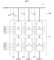
- FIG. 2 is a diagram showing each wiring electrically connected to a pixel circuit included in the display device of Embodiment 1 shown in FIG. 1.
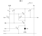
- FIG. 2 is a circuit diagram showing a pixel circuit included in the display device of Embodiment 1 shown in FIG. 1.
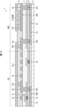
- FIG. 2 is a cross-sectional view showing a schematic configuration of a portion where a data signal line is electrically connected to a high-potential side power supply voltage wiring via a pull-up resistor in the display device of Embodiment 1 shown in FIG. 1.
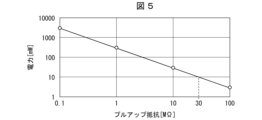
- FIG. 2 is a diagram for explaining a preferable resistance value of a pull-up resistor when the power consumption of the display device of Embodiment 1 shown in FIG. 1 is taken into account.
- FIG. 2 is a diagram for explaining a preferable resistance value of a pull-up resistor when the charging rate of the data signal line of the display device of the first embodiment shown in FIG. 1 is taken into consideration.
- FIG. 2 is a diagram for explaining a preferable resistance value of a pull-up resistor when considering charging the data signal line to 99% within one frame period of the display device of Embodiment 1 shown in FIG. 1;
- 3 is a diagram illustrating a schematic configuration of a display device according to a second embodiment.
- FIG. 12 is a diagram illustrating a schematic configuration of a display device according to a third embodiment.
- FIG. FIG. 7 is a diagram showing a schematic configuration of a display device according to a fourth embodiment.
- 12 is a circuit diagram showing a pixel circuit included in a display device of Embodiment 5.
- FIGS. 1 to 11 The embodiment of the present disclosure will be described below based on FIGS. 1 to 11.
- components having the same functions as those described in a specific embodiment will be denoted by the same reference numerals, and the description thereof may be omitted.
- FIG. 1 is a plan view showing a schematic configuration of a display device 1 according to the first embodiment.
- the display device 1 includes a plurality of data signal lines DLn (n is a natural number of 2 or more, and only one of the plurality of data signal lines is shown in FIG. 1), and a plurality of A display area DA including a scanning signal line GLm (m is a natural number of 2 or more, and only one of the plurality of scanning signal lines is shown in FIG. 1), and a frame area NDA surrounding the display area DA. It is equipped with
- the first high-potential side power supply voltage wiring (high-potential side power supply voltage wiring) to which the data signal line DLn is electrically connected via the pull-up resistor R1 is , the first high-potential side power supply voltage main wiring ELVDDM provided in the frame area NDA so as to surround the upper end, left end, and right end of the display area DA, and the first high potential side power supply voltage main wiring ELVDDM. It is connected to a pixel circuit GC (m, n) provided in the display area DA and is configured with a first high-potential power supply voltage branch wiring ELVDDEn provided in the display area DA and the frame area NDA.
- the wiring supplies a high-potential side power supply voltage
- the wiring is not limited to this.
- a second high potential side power supply voltage wiring GVDD provided in the frame area NDA so as to surround the right end portion, and supplies a high potential side power supply voltage to a scanning side drive circuit (not shown) provided in the frame area NDA. It may be wiring.
- the first high-potential side power supply voltage trunk wiring ELVDDM and the first high-potential side power supply voltage branch wiring ELVDDEn are connected to a terminal portion TR to which one end of the first high-potential side power supply voltage trunk wiring ELVDDM is electrically connected.
- the first terminal for the first high potential side power supply voltage and the second terminal for the first high potential side power supply voltage of the terminal portion TR to which the other end of the first high potential side power supply voltage main wiring ELVDDM are electrically connected.
- the pull-up resistor R1 is electrically connected to the end of the data signal line DLn that is far from the bent portion FR, and the data signal line DLn is connected to the frame area.
- the first high-potential side power supply voltage trunk line ELVDDM which is the first high-potential side power supply voltage line provided in the NDA, is electrically connected via a pull-up resistor R1. It is not limited to this.
- the data signal line DLn is pulled up to a first high-potential side power supply voltage wiring, which is an example of a high-potential side power supply voltage wiring, for example, a wiring that supplies a high-potential side power supply voltage to the pixel circuit GC (m, n). It is sufficient that the data signal line DLn is electrically connected to the frame area NDA via the pull-up resistor R1, although it is not shown in the figure.
- the data signal line DLn may be electrically connected to the wiring ELVDDEn, and the data signal line DLn may be electrically connected to the first high potential side power supply voltage branch wiring ELVDDEn provided in the display area DA via a pull-up resistor R1. Good too.
- the frame area NDA of the display device 1 is electrically connected to the data signal line DLn and a bending portion FR provided to intersect the extending direction D1 of the data signal line DLn. FR.
- the bent portion FR is provided along the extending direction D2 of the scanning signal line GLm and perpendicular to the extending direction D1 of the data signal line DLn, but is not limited to this. It will not be done.
- the bent portion FR is formed by forming an inorganic film in a part of a region where a gate insulating film 4, a first inorganic insulating film 6, and a second inorganic insulating film 7 are laminated in this order on the substrate 2.
- the gate insulating film 4, the first inorganic insulating film 6, and the second inorganic insulating film 7, which are films, are removed to form an opening region, and this opening region is filled with a first organic insulating film 9.
- the present invention is not limited to this.
- the substrate 2 is not limited to the resin substrate as long as it is a flexible substrate. do not have.
- the folding portion FR provided in the display device 1 is composed of the substrate 2, which is a resin substrate, and the first organic insulating film 9, the display device 1 can be easily folded at the folding portion FR. Can be done.
- the video wiring VLn spanning the bent portion FR is formed on the first organic insulating film 9 using the same material as the data signal line DLn, in the process of forming the data signal line DLn.
- one end of the video wiring VLn is electrically connected to the data signal line DLn, and the other end of the video wiring VLn is connected to the n-th data signal supply terminal of the terminal portion TR. electrically connected.
- a corresponding data signal is supplied from a scanning side drive circuit (not shown) to the n-th data signal supply terminal of the terminal portion TR.
- the wiring spanning the bent portion FR includes a first high-potential side power supply voltage main wiring ELVDDM and a low-potential side power supply voltage wiring for supplying a low-level power supply voltage ELVSS (not shown). etc. are included.
- FIG. 2 is a diagram showing each wiring electrically connected to the pixel circuit GC included in the display device 1 of the first embodiment shown in FIG.
- the display device 1 is provided with pixel circuits GC(1,1) to GC(m,n) corresponding to m ⁇ n pixels provided in the display area DA.
- the scanning signal line GLm and the data signal line DLn which is electrically connected via the pull-up resistor R1 to the first high potential side power supply voltage main wiring ELVDDM provided in the frame area NDA, are electrically connected to each other.
- the connected pixel circuit GC (m, n) has a scanning signal line GLm-1 and a line for supplying the high potential side power supply voltage necessary for driving the pixel circuit GC (m, n).
- a second initialization voltage wiring Vini2 for supplying the voltage is electrically connected to the second initialization voltage wiring Vini2.
- FIG. 3 is a circuit diagram showing the pixel circuit GC(m,n) included in the display device 1 of the first embodiment shown in FIG.
- the pixel circuit GC (m, n) includes one OLED (organic light emitting diode) or QLED (quantum dot light emitting diode) as a light emitting element LED, and seven transistors T1 to T7. and one holding capacitor C1.
- OLED organic light emitting diode
- QLED quantum dot light emitting diode
- the pixel circuit GC (m, n) is composed of one light emitting element LED, seven transistors T1 to T7, and one holding capacitor C1.
- Transistor T1 is a first initialization transistor
- transistor T2 is a threshold compensation transistor
- transistor T3 is a write control transistor
- transistor T4 is a drive transistor
- transistor T5 is a first emission control transistor
- T6 is a second light emission control transistor
- transistor T7 is a second initialization transistor. Note that in the pixel circuit GC (m, n), the transistors T1 to T3 and the transistors T5 to T7, other than the transistor T4 which is a driving transistor, function as switching elements.
- each of the transistors T1 to T7 included in the pixel circuit GC (m, n) is a P-type transistor, and each of the transistors T1 to T7, which is a P-type transistor, is formed using a polycrystalline silicon layer as a semiconductor layer.
- the description will be given as an example of a case where the system is equipped with the following, the present invention is not limited to this.
- each of the transistors T1 to T7 included in the pixel circuit GC (m, n) is an N-type transistor, and each of the transistors T1 to T7, which is an N-type transistor, includes an oxide semiconductor layer as a semiconductor layer.
- the transistors T1 to T7 included in the pixel circuit GC are P-type transistors, the remaining transistors are N-type transistors, and some of the transistors are P-type transistors.
- the transistor may include a polycrystalline silicon layer as a semiconductor layer, and the remaining transistors, which are N-type transistors, may include an oxide semiconductor layer as a semiconductor layer.
- the m-th scanning signal output from a scanning side drive circuit (not shown) is supplied to the gate electrode of the transistor T2 and the gate electrode of the transistor T3 via the scanning signal line GLm. .
- the m-th light emission control signal output from a light emission control circuit (emission driver) not shown is supplied to the gate electrode of the transistor T5 and the gate electrode of the transistor T6 via the light emission control wiring EMm.
- the high-level power supply voltage ELVDD is supplied to a power supply (not shown) via the first high-potential side power supply voltage main wiring ELVDDM and the first high-potential side power supply voltage branch wiring ELVDDEn shown in FIG. 2, which are high-potential side power supply voltage wirings.
- the low level power supply voltage ELVSS is supplied from a power supply circuit (not shown) via a low potential side power supply voltage wiring (not shown), and the first initialization voltage is supplied from a power supply circuit (not shown) through a first initialization voltage wiring Vini1.
- the second initialization voltage is supplied from a power supply circuit (not shown) via a second initialization voltage wiring Vini2.
- the source electrode of the transistor T3 is supplied with an n-th data signal output from a data side drive circuit (not shown) via a data signal line DLn.
- the gate electrode of the transistor T1 is supplied with the m-1th scanning signal output from the scanning side drive circuit (not shown) via the scanning signal line GLm-1, and the gate electrode of the transistor T1
- the drain electrode of the transistor T1 is connected to one side electrode of the holding capacitor C1, the gate electrode of the transistor T4, and the source electrode of the transistor T2, and the source electrode of the transistor T1 is connected to a first initialization voltage that is supplied with a first initialization voltage. It is electrically connected to voltage wiring Vini1.
- the gate electrode of the transistor T2 is electrically connected to the scanning signal line GLm to which the m-th scanning signal is supplied, and the drain electrode of the transistor T2 is electrically connected to the drain electrode of the transistor T4 and the source electrode of the transistor T6.
- the source electrode of transistor T2 is electrically connected to the gate electrode of transistor T4.
- the gate electrode of the transistor T3 is electrically connected to the scanning signal line GLm to which the m-th scanning signal is supplied, and the source electrode of the transistor T3 is electrically connected to the data signal line DLn to which the n-th data signal is supplied.
- the drain electrode of the transistor T3 is electrically connected to the source electrode of the transistor T4 and the drain electrode of the transistor T5.
- the gate electrode of the transistor T4 is electrically connected to one electrode of the holding capacitor C1 and the source electrode of the transistor T2, and the source electrode of the transistor T4 is connected to the drain electrode of the transistor T3 and the drain electrode of the transistor T5.
- the drain electrode of the transistor T4 is electrically connected to the source electrode of the transistor T6.
- the gate electrode of the transistor T5 is electrically connected to the emission control wiring EMm to which the m-th emission control signal is supplied, and the source electrode of the transistor T5 is connected to the high-potential side power supply voltage wiring to which the high-level power supply voltage ELVDD is supplied.
- the drain electrode of the transistor T5 is electrically connected to the drain electrode of the transistor T3 and the source electrode of the transistor T4.
- the gate electrode of the transistor T6 is electrically connected to the emission control wiring EMm to which the m-th emission control signal is supplied, the source electrode of the transistor T6 is electrically connected to the drain electrode of the transistor T4, and the transistor The drain electrode of T6 is electrically connected to the anode electrode of the light emitting element LED.
- the gate electrode of the transistor T7 is electrically connected to the scanning signal line GLm to which the m-th scanning signal is supplied, and the source electrode of the transistor T7 is connected to the second initialization voltage line Vini2 to which the second initialization voltage is supplied.
- the drain electrode of the transistor T7 is electrically connected to the anode electrode of the light emitting element LED.
- the other electrode of the holding capacitor C1 is electrically connected to a high-potential side power supply voltage wiring to which a high-level power supply voltage ELVDD is supplied.
- a cathode electrode of the light emitting element LED is electrically connected to a low potential side power supply voltage wiring to which a low level power supply voltage ELVSS is supplied.
- the gate electrode of the transistor T1 may be electrically connected to the scanning signal line GLm-2 to which the m-2th scanning signal is supplied.
- the case where the gate electrode of the transistor T7 is electrically connected to the scanning signal line GLm to which the m-th scanning signal is supplied has been described as an example, but the present invention is not limited to this. Instead, the gate electrode of the transistor T7 may be electrically connected to the discharge signal line to which the m-th discharge signal is supplied.
- the display device 1 shown in FIG. 1 by folding the display device 1 at the above-mentioned bending portion FR, it is possible to realize a narrow frame in which the frame area NDA can be made smaller without reducing the width of the frame area NDA.
- the video wiring VLn spanning the bending portion FR may be disconnected due to cracks or the like generated in the bending step.
- each of the data signal lines DLn electrically connected to each of the video wiring VLn spanning the bent portion FR is It is electrically connected to a first high-potential side power supply voltage main wiring ELVDDM provided in the frame area NDA via a pull-up resistor R1. Therefore, even if a disconnection occurs in the video wiring VLn spanning the bent portion FR, the data signal line DLn electrically connected to the video wiring VLn will not be in a floating state. By preventing the data signal line DLn that is electrically connected to the video line VLn from being in a floating state, it is possible to suppress the flow of current that greatly exceeds the current normally expected in these lines.
- This display reduces the possibility of non-repairable malfunctions such as brightness display, heat generation, and smoke generation, and improves the possibility of normal operation by repairing the disconnected part of the video wiring VLn that straddles the bent part FR.
- Device 1 can be realized.
- all of the data signal lines DLn electrically connected to each of the video wirings VLn that straddle the bent portion FR are connected to the frame area via the pull-up resistor R1.
- An example will be described in which the video wiring VLn is electrically connected to the first high-potential side power supply voltage main wiring ELVDDM provided in the NDA, but the present invention is not limited thereto.
- One or more of the data signal lines DLn electrically connected to each one of the data signal lines DLn are connected to a first high potential side power supply voltage main provided in the frame area NDA via a pull-up resistor R1. If it is electrically connected to the wiring ELVDDM, it is possible to reduce the possibility of non-repairable problems such as high brightness display, heat generation, and smoke generation.
- each data signal line DLn which is electrically connected to each video wiring VLn that straddles the bent portion FR, is connected to the high potential side power supply voltage wiring via a pull-up resistor. There was no electrical connection. Therefore, if a disconnection occurs in the video wiring VLn spanning the bent portion FR, a portion of the video wiring VLn electrically connected to the data signal line DLn and the data signal line DLn will be in a floating state.
- the video voltage (for example, +2V to +7V) that should originally be written is not written to the gate electrode of the transistor T4 of each pixel circuit GC (1, n) to GC (m, n), and the pixel circuit GC (1, , n) to GC(m, n) are maintained at a voltage near the first initialization voltage. Since the first initialization voltage is approximately -4V to -5V, a large current flows between the source electrode and the drain electrode in each transistor T4 of the pixel circuits GC(1,n) to GC(m,n). As a result, high brightness display (high brightness light emission) occurs in the light emitting elements LED provided in each of the pixel circuits GC(1,n) to GC(m,n).
- the low-potential side power supply voltage wiring provided in the bent portion FR is most affected by the large current, and is likely to generate heat and smoke.
- a disconnection occurs in the low-potential side power supply voltage wiring of the bent part FR during the bending process, or if a disconnection occurs in the low-potential side power supply voltage wiring of the bent part FR due to the effects of smoke or heat generation mentioned above, Current will further concentrate on the normal low-potential side power supply voltage wiring that is not disconnected in the section FR, and the degree of heat generation and smoke generation will become worse.
- each of the data signal lines DLn which are electrically connected to each video wiring VLn that straddles the bent portion FR, is electrically connected to the high potential side power supply voltage wiring via a pull-up resistor.
- problems that cannot be repaired such as high brightness display (high brightness light emission), heat generation, and smoke will occur.
- the broken portion of the video wiring VLn spanning the bent portion FR cannot be reduced and the broken portion of the video wiring VLn is repaired, there is a high possibility that the display device will not be able to operate normally.
- FIG. 4 shows that in the display device 1 of Embodiment 1 shown in FIG. 1, the data signal line DLn is electrically connected to the first high-potential side power supply voltage trunk line ELVDDM, which is the high-potential side power supply voltage line, via the pull-up resistor R1.
- FIG. 3 is a cross-sectional view showing a schematic configuration of connected parts.
- the display device 1 includes a shield portion SHE electrically connected to a first high-potential side power supply voltage main wiring ELVDDM, which is a high-potential side power supply voltage wiring.
- the shield part SHE is arranged between the first high-potential side power supply voltage main wiring ELVDDM, which is a high-potential side power supply voltage wiring, and the pull-up resistor R1, and overlaps with at least a part of the pull-up resistor R1. It is set up to do so.
- the shield part SHE that is electrically connected to the first high potential side power supply voltage main wiring ELVDDM, which is the high potential side power supply voltage wiring, and maintained at the first high potential side power supply voltage, it is possible to The influence of the electric field of the wiring and the influence of the capacitance of various insulating films can be reduced by the shield part SHE, and it is possible to create a structure that is only affected by the stable high potential from the shield part SHE.
- the first high-potential side power supply voltage main wiring ELVDDM which is the high-potential side power supply voltage wiring
- the pull-up resistor R1 are connected to each other through the shield part SHE.
- the explanation will be given as an example of a case in which the main power supply voltage wiring ELVDDM on the high potential side, which is the power supply voltage wiring on the high potential side, and the pull-up resistor R1 are not limited to this.
- the shield part SHE may be electrically connected via a conductive member other than the shield part SHE, and the first high-potential side power supply voltage main wiring ELVDDM, which is the high-potential side power supply voltage wiring, and the pull-up resistor R1 are in direct contact with each other. It's okay.
- the substrate 2 which is a flexible substrate
- semiconductor layers 3a and 3b there are semiconductor layers 3a and 3b, a gate insulating film 4, and first conductive layers 5a and 5b.
- a third conductive layer forming the power supply voltage trunk line ELVDDM is provided in this order from the substrate 2 side.
- a second organic insulating film is provided on the third conductive layer and the first organic insulating film 9 that form the data signal line DLn and the first high-potential side power supply voltage main line ELVDDM.
- a fourth conductive layer forming an anode electrode of the light emitting element LED shown in FIG. 3 is provided on the second organic insulating film in the display area DA.
- a third organic insulating film is provided on the second organic insulating film.
- the semiconductor layer (first semiconductor layer) 3a is a semiconductor layer included in the transistor T3 whose source electrode is electrically connected to the data signal line DLn, as shown in FIG.
- Layer 3b is the pull-up resistor R1 shown in FIGS. 1 and 2.
- the pull-up resistor R1 By forming the pull-up resistor R1 using a polycrystalline silicon layer in this manner, it is possible to provide the pull-up resistor R1 having a relatively high resistance value.
- the semiconductor layer 3a provided in the transistor T3 is a semiconductor layer in which a portion of a polycrystalline silicon layer is doped with an impurity to form a source region and a drain region, but the semiconductor layer 3b functioning as a pull-up resistor R1 is
- the polycrystalline silicon layer is a semiconductor layer that is not doped with impurities.
- the semiconductor layer 3b forming the pull-up resistor R1 has a source electrode (first input electrode) electrically connected to the data signal line DLn and a semiconductor layer (first semiconductor layer) that is electrically connected to the data signal line DLn.
- the semiconductor layer (first semiconductor layer) 3a provided in the transistor (first transistor) T3 including the layer 3a is made of the same material.
- the present invention is not limited to this.
- the pixel circuit GC (m, n) includes a source electrode (first input electrode) electrically connected to the data signal line DLn, a semiconductor layer (first semiconductor layer) 3a, and a semiconductor layer (first semiconductor layer) 3a.
- the semiconductor layer 3b forming the pull-up resistor R1 is a semiconductor layer (second semiconductor layer) included in the transistor (second transistor, one of T1, T2, T4 to T7). may be made of the same material.
- the first conductive layer 5a is a gate electrode provided in the transistor (first transistor) T3, and the first conductive layer 5b is a wiring.
- the second conductive layer 8b is a source electrode provided in the transistor (first transistor) T3
- the second conductive layer 8d is a data
- the second conductive layer 8e is a first conductive member that electrically connects the signal line DLn and the pull-up resistor R1, and the second conductive layer 8e electrically connects the pull-up resistor R1 and the first high-potential side power supply voltage trunk wiring ELVDDM. It is a second conductive member and a shield part SHE, and the second conductive layer 8a and the second conductive layer 8c are wirings.
- the second conductive layer 8e which is the second conductive member and the shield part SHE, is composed of the gate insulating film 4, the first inorganic insulating film 6, and the second inorganic insulating film 7.
- a second conductive layer 8d which is a first conductive member, is also formed in the first contact hole CO1 formed in the gate insulating film 4, the first inorganic insulating film 6, and the second inorganic insulating film 7.
- a second contact hole CO2 is also formed in which the second conductive layer 8b serving as the source electrode is connected to the third contact hole formed in the gate insulating film 4, the first inorganic insulating film 6, and the second inorganic insulating film 7.
- the explanation will be given by taking as an example a case in which it is also formed in CO3, but the invention is not limited to this.
- other conductive members may be formed in the first contact hole CO1, the second contact hole CO2, and the third contact hole CO3.
- the first high-potential side power supply voltage main wiring ELVDDM shown in FIG. By contacting the second conductive layer 8e, the first high potential side power supply voltage main wiring ELVDDM and the second conductive layer 8e are electrically connected.
- the data signal line DLn shown in FIG. It is electrically connected to the second conductive layer 8d. Furthermore, the data signal line DLn shown in FIG. It is electrically connected to the second conductive layer 8b.
- FIG. 5 is a diagram for explaining a preferable resistance value of the pull-up resistor R1 when the power consumption of the display device 1 of the first embodiment shown in FIG. 1 is taken into account.
- the resistance value of the pull-up resistor R1 is preferably 30 M ⁇ or more.
- FIG. 6 is a diagram for explaining a preferable resistance value of the pull-up resistor R1 when the charging rate of the data signal line DLn of the display device 1 of the first embodiment shown in FIG. 1 is considered.
- the charging rate of both the part of the data signal line DLn far from the terminal part TR when there is a pull-up resistor R1 and the part of the data signal line DLn near the terminal part TR is the same as that of the part without the pull-up resistor R1.
- the pull-up resistor R1 can be approximately equal to the charging rate, that is, the pull-up resistor R1 can be made to a level that does not interfere with the charging rate
- the resistance value of the pull-up resistor R1 is preferably 50 M ⁇ or more, as shown in FIG.
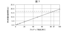
- FIG. 7 is a diagram illustrating a preferable resistance value of the pull-up resistor R1 when considering charging the data signal line DLn to 99% within one frame period of the display device 1 of the first embodiment shown in FIG. It is a diagram.
- the resistance value of the pull-up resistor R1 is 87 M ⁇ or less. It is preferable that there be.
- the resistance value of the pull-up resistor R1 is preferably 30 M ⁇ or more and 87 M ⁇ or less, and more preferably 50 M ⁇ or more and 80 M ⁇ or less.
- the high potential side power supply voltage wiring to which the data signal line DLn is electrically connected via the pull-up resistor R1 is the second high potential side power supply voltage wiring GVDD
- the second high potential side power supply voltage wiring GVDD is the second high potential side power supply voltage wiring GVDD.
- the potential side power supply voltage wiring GVDD is different from the display device 1 of the first embodiment described above in that the potential side power supply voltage wiring GVDD is a wiring that supplies a high potential side power supply voltage to a scanning side drive circuit (not shown) provided in the frame area NDA.
- Other details are as described in the first embodiment. For convenience of explanation, members having the same functions as those shown in the drawings of Embodiment 1 are given the same reference numerals, and the explanation thereof will be omitted.
- FIG. 8 is a diagram showing a schematic configuration of a display device 1a according to the second embodiment.
- the high potential side power supply voltage wiring to which the data signal line DLn is electrically connected via the pull-up resistor R1 is the second high potential side power supply voltage wiring GVDD
- the second high potential side power supply voltage wiring GVDD is a wiring that supplies a high potential side power supply voltage to a scanning side drive circuit (not shown) provided in the frame area NDA.
- the display device 1a even if a disconnection occurs in the video wiring VLn spanning the bent portion FR, the data signal line DLn electrically connected to the video wiring VLn does not enter a floating state.
- the data signal line DLn electrically connected to the video line VLn By preventing the data signal line DLn electrically connected to the video line VLn from being in a floating state, it is possible to suppress the flow of a current that greatly exceeds the current normally expected in these lines.
- This display reduces the possibility of non-repairable malfunctions such as brightness display, heat generation, and smoke generation, and improves the possibility of normal operation by repairing the disconnected part of the video wiring VLn that straddles the bent part FR.
- the device 1a can be realized.
- the display device 1a is electrically connected to a second high potential power supply voltage wiring GVDD, which is a high potential power supply voltage wiring, and has a shield that is maintained at the second high potential power supply voltage.
- GVDD a high potential power supply voltage wiring
- the shield part SHE By providing the shield part SHE, the influence of the electric field of other wirings and the influence of the electrostatic capacitance of various insulating films is reduced by the shield part SHE, and the configuration is such that the shield part SHE is only influenced by the stable high potential from the shield part SHE. Can be done.
- the display device 1b of this embodiment includes a first high-potential side power supply voltage trunk line ELVDDM provided in the frame area NDA and a first high-potential side power supply voltage main line ELVDDM provided in the display area DA and frame area NDA as the high-potential side power supply voltage line. It includes a first high potential side power supply voltage wiring including a potential side power supply voltage branch wiring ELVDDEn, and a second high potential side power supply voltage wiring GVDD provided in the frame area NDA, and a bent portion FR as a pull-up resistor.
- the first pull-up resistor R1 is electrically connected to the end of the data signal line DLn that is farthest from the data signal line DLn, and the second pull-up resistor R2 is connected in series to the first pull-up resistor R1.
- the signal line DLn is different from the display devices 1 and 1a of the first and second embodiments described above in that the signal line DLn is electrically connected to the second high-potential side power supply voltage wiring GVDD via the above-described pull-up resistor.
- the other details are as described in the first and second embodiments. For convenience of explanation, members having the same functions as those shown in the drawings of Embodiments 1 and 2 are given the same reference numerals, and their explanations are omitted.
- FIG. 9 is a diagram showing a schematic configuration of the display device 1b of Embodiment 3.
- the display device 1b includes a first high-potential side power supply voltage trunk line ELVDDM provided in the frame area NDA, and a first high-potential side power supply voltage trunk line ELVDDM provided in the display area DA and frame area NDA as the high-potential side power supply voltage line. It includes a first high potential side power supply voltage wiring including a first high potential side power supply voltage branch wiring ELVDDEn, and a second high potential side power supply voltage wiring GVDD provided in the frame area NDA.
- the display device 1b also includes, as a pull-up resistor, a first pull-up resistor R1 electrically connected to the end of the data signal line DLn that is far from the bent portion FR, and a first pull-up resistor R1 connected in series with the first pull-up resistor R1.
- the data signal line DLn is connected to the second high-potential side power supply via the above-mentioned pull-up resistors, that is, the first pull-up resistor R1 and the second pull-up resistor R2. It is electrically connected to voltage wiring GVDD.
- the resistance value of the pull-up resistor in which the first pull-up resistor R1 and the second pull-up resistor R2 are connected in series is the resistance value of the first pull-up resistor R1 and the resistance value of the second pull-up resistor R2. This is the combined value.
- the display device 1b even if a disconnection occurs in the video wiring VLn spanning the bent portion FR, the data signal line DLn electrically connected to the video wiring VLn does not enter a floating state.
- the data signal line DLn electrically connected to the video line VLn By preventing the data signal line DLn electrically connected to the video line VLn from being in a floating state, it is possible to suppress the flow of a current that greatly exceeds the current normally expected in these lines.
- This display reduces the possibility of non-repairable malfunctions such as brightness display, heat generation, and smoke generation, and improves the possibility of normal operation by repairing the disconnected part of the video wiring VLn that straddles the bent part FR.
- the device 1b can be realized.
- the display device 1b includes a first shield portion SHE1 electrically connected to a second high potential side power supply voltage wiring GVDD, and a first high potential side power supply voltage wiring that is a first high potential side power supply voltage wiring. It includes a second shield part SHE2 electrically connected to the power supply voltage main wiring ELVDDM. As in the case shown in FIG. 4, the first shield part SHE1 is arranged between the second high-potential side power supply voltage wiring GVDD and the first pull-up resistor R1, and overlaps with at least a part of the first pull-up resistor R1. Similarly to the case shown in FIG.
- the second shield part CHE2 also connects the first high-potential side power supply voltage main wiring ELVDDM, which is the first high-potential side power supply voltage wiring, and the second pull-up resistor R2.
- the second pull-up resistor R2 is provided so as to overlap with at least a portion of the second pull-up resistor R2.
- the second high-potential side power supply voltage wiring GVDD and the first pull-up resistor R1 shown in FIG. 9 may be electrically connected via the first shield part SHE1, as in the case shown in FIG.
- the first high-potential side power supply voltage main wiring ELVDDM which is the first high-potential side power supply voltage wiring shown in FIG. may be electrically connected.
- the display device 1b includes a first shield portion SHE1 that is electrically connected to the second high-potential side power supply voltage wiring GVDD and maintained at the second high-potential side power supply voltage, and a first shield portion SHE1 that is the first high-potential side power supply voltage wiring.
- a second shield part SHE2 that is electrically connected to the first high-potential side power supply voltage main wiring ELVDDM and maintained at the first high-potential side power supply voltage, it is possible to prevent the influence of electric fields of other wirings and the effects of various insulating films.
- the influence of capacitance can be reduced by the first shield part SHE1 and the second shield part SHE2, and a configuration can be achieved in which only the influence of stable high potential from the first shield part SHE1 and the second shield part SHE2 is received.
- the data signal line DLn is connected to the first high voltage line, which is the first high potential side power supply voltage wiring, via the first pull-up resistor R1 and the second pull-up resistor R2 connected in series.
- the display device 1b differs from the display device 1b of the third embodiment described above in that it is electrically connected to the potential-side power supply voltage trunk line ELVDDM.
- ELVDDM potential-side power supply voltage trunk line
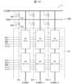
- FIG. 10 is a diagram showing a schematic configuration of a display device 1c according to the fourth embodiment.
- the display device 1c includes a first high-potential side power supply voltage main wiring ELVDDM provided in the frame area NDA as a high-potential side power supply voltage wiring, and a first high-potential side power supply voltage main wiring ELVDDM provided in the display area DA and the frame area NDA. It includes a first high potential side power supply voltage wiring including a first high potential side power supply voltage branch wiring ELVDDEn, and a second high potential side power supply voltage wiring GVDD provided in the frame area NDA.
- the display device 1c also includes, as a pull-up resistor, a first pull-up resistor R1 electrically connected to the end of the data signal line DLn that is far from the bent portion FR, and a first pull-up resistor R1 connected in series with the first pull-up resistor R1.
- the data signal line DLn is connected to the first high-potential side power supply via the above-mentioned pull-up resistors, that is, the first pull-up resistor R1 and the second pull-up resistor R2. It is electrically connected to a first high-potential side power supply voltage main wiring ELVDDM, which is a voltage wiring.
- the display device 1c even if a disconnection occurs in the video wiring VLn spanning the bent portion FR, the data signal line DLn electrically connected to the video wiring VLn does not enter a floating state.
- the data signal line DLn that is electrically connected to the video line VLn By preventing the data signal line DLn that is electrically connected to the video line VLn from being in a floating state, it is possible to suppress the flow of current that greatly exceeds the current normally expected in these lines.
- This display reduces the possibility of non-repairable malfunctions such as brightness display, heat generation, and smoke generation, and improves the possibility of normal operation by repairing the disconnected part of the video wiring VLn that straddles the bent part FR.
- a device 1c can be realized.
- the display device 1c includes a first shield portion SHE1 electrically connected to a first high potential side power supply voltage main wiring ELVDDM, which is a first high potential side power supply voltage wiring, and a second high potential side power supply voltage main wiring ELVDDM. It includes a second shield part SHE2 electrically connected to the side power supply voltage wiring GVDD.
- the first shield part SHE1 is arranged between the first high-potential side power supply voltage main wiring ELVDDM and the first pull-up resistor R1, and overlaps with at least a part of the first pull-up resistor R1.
- the second shield part CHE2 also includes a second pull-up resistor between the second high-potential side power supply voltage wiring GVDD and the second pull-up resistor R2. It is provided so as to overlap at least a portion of R2.
- the first high-potential side power supply voltage main wiring ELVDDM and the first pull-up resistor R1 shown in FIG. 10 may be electrically connected via the first shield part SHE1, as in the case shown in FIG.
- the second high-potential side power supply voltage wiring GVDD and the second pull-up resistor R2 shown in FIG. 10 may be electrically connected via the second shield part SHE2, as in the case shown in FIG. .
- the display device 1c includes a first shield portion SHE1 that is electrically connected to a first high-potential side power supply voltage trunk line ELVDDM, which is a first high-potential side power supply voltage line, and is maintained at the first high-potential side power supply voltage;
- a second shield part SHE2 that is electrically connected to the second high-potential side power supply voltage wiring GVDD and maintained at the second high-potential side power supply voltage, it is possible to prevent the influence of electric fields of other wirings,
- the influence of capacitance can be reduced by the first shield part SHE1 and the second shield part SHE2, and a configuration can be achieved in which only the influence of stable high potential from the first shield part SHE1 and the second shield part SHE2 is received.
- Embodiment 5 of the present disclosure will be described based on FIG. 11.
- the pixel circuit GC'(m, n) included in the display device of this embodiment has the following points: P-type transistors T3 to T6 and N-type transistors T1, T2, and T7. This is different from the display device 1 of the first embodiment described above, which includes a pixel circuit GC (m, n) including only transistors T1 to T7, which are type transistors. Other details are as described in the first embodiment. For convenience of explanation, members having the same functions as those shown in the drawings of Embodiment 1 are given the same reference numerals, and the explanation thereof will be omitted.
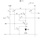
- FIG. 11 is a circuit diagram showing a pixel circuit GC'(m,n) included in the display device of Embodiment 5.
- transistors T3 to T6 included in the pixel circuit GC'(m, n) are P-type transistors, and transistors T1, T2, and T7 are N-type transistors.
- Each of transistors T3 to T6, which are P-type transistors includes a polycrystalline silicon layer as a semiconductor layer (first semiconductor layer), and each of transistors T1, T2, and T7, which is an N-type transistor, includes a semiconductor layer (second semiconductor layer).
- the semiconductor layer forming the pull-up resistor is the same as the polycrystalline silicon layer described above or the oxide semiconductor layer described above. It can be made of any material.
- the scanning signal for driving the m-2nd N-type transistor is connected to the gate electrode of the transistor T1, which is an N-type transistor, on the scanning signal line for driving the N-type transistor.
- a scan signal for driving the m-th N-type transistor is supplied to the gate electrode of the transistor T2, which is an N-type transistor, via the scan signal line GLm-2' for driving the N-type transistor. .
- the pixel circuit GC'(m, n) shown in FIG. 11 is different from the pixel circuit GC(m, n) shown in FIG. 3 in that one initialization voltage is supplied via the initialization voltage wiring Vini. It is different from.
- N1 is the first node
- N2 is the second node
- Vg is the voltage of the gate electrode of the transistor T4
- Va is the voltage of the anode electrode of the light emitting element LED
- I1 is the voltage of the anode electrode of the light emitting element LED. This is the current flowing through the transistor T6.
- the present disclosure can be used for display devices.
Landscapes
- Engineering & Computer Science (AREA)
- Physics & Mathematics (AREA)
- General Physics & Mathematics (AREA)
- Theoretical Computer Science (AREA)
- Computer Hardware Design (AREA)
- Devices For Indicating Variable Information By Combining Individual Elements (AREA)
- Electroluminescent Light Sources (AREA)
- Control Of Indicators Other Than Cathode Ray Tubes (AREA)
Abstract
Description
データ信号線を含む表示領域及び前記表示領域を囲む額縁領域と、
少なくとも前記額縁領域に設けられた高電位側電源電圧配線と、を備え、
前記額縁領域は、前記データ信号線の延在方向と交差するように設けられた折り曲げ部と、前記データ信号線と電気的に接続され、前記折り曲げ部を跨ぐビデオ配線とを含み、
前記データ信号線は、前記高電位側電源電圧配線にプルアップ抵抗を介して電気的に接続されている。
図1は、実施形態1の表示装置1の概略的な構成を示す平面図である。
次に、図8に基づき、本開示の実施形態2について説明する。本実施形態の表示装置1aにおいては、データ信号線DLnがプルアップ抵抗R1を介して電気的に接続された高電位側電源電圧配線が第2高電位側電源電圧配線GVDDであり、第2高電位側電源電圧配線GVDDは額縁領域NDAに設けられた図示していない走査側駆動回路に高電位側電源電圧を供給する配線である点において、上述した実施形態1の表示装置1とは異なる。その他については実施形態1において説明したとおりである。説明の便宜上、実施形態1の図面に示した部材と同じ機能を有する部材については、同じ符号を付し、その説明を省略する。
次に、図9に基づき、本開示の実施形態3について説明する。本実施形態の表示装置1bは、高電位側電源電圧配線として、額縁領域NDAに設けられた第1高電位側電源電圧幹配線ELVDDMと、表示領域DA及び額縁領域NDAに設けられた第1高電位側電源電圧枝配線ELVDDEnとを含む第1高電位側電源電圧配線と、額縁領域NDAに設けられた第2高電位側電源電圧配線GVDDとを備えており、プルアップ抵抗として、折り曲げ部FRから遠い方のデータ信号線DLnの端部に電気的に接続された第1プルアップ抵抗R1と、第1プルアップ抵抗R1に直列接続された第2プルアップ抵抗R2とを備えており、データ信号線DLnは、上述したプルアップ抵抗を介して第2高電位側電源電圧配線GVDDに電気的に接続されている点において、上述した実施形態1及び2の表示装置1・1aとは異なる。その他については実施形態1及び2において説明したとおりである。説明の便宜上、実施形態1及び2の図面に示した部材と同じ機能を有する部材については、同じ符号を付し、その説明を省略する。
次に、図10に基づき、本開示の実施形態4について説明する。本実施形態の表示装置1cにおいては、データ信号線DLnは、直列接続された第1プルアップ抵抗R1と第2プルアップ抵抗R2とを介して第1高電位側電源電圧配線である第1高電位側電源電圧幹配線ELVDDMに電気的に接続されている点において、上述した実施形態3の表示装置1bとは異なる。その他については実施形態3において説明したとおりである。説明の便宜上、実施形態3の図面に示した部材と同じ機能を有する部材については、同じ符号を付し、その説明を省略する。
次に、図11に基づき、本開示の実施形態5について説明する。本実施形態の表示装置に備えられた画素回路GC’(m、n)は、P型トランジスタであるトランジスタT3~T6と、N型トランジスタであるトランジスタT1・T2・T7とを含む点において、P型トランジスタであるトランジスタT1~T7のみを含む画素回路GC(m、n)を備えた上述した実施形態1の表示装置1とは異なる。その他については実施形態1において説明したとおりである。説明の便宜上、実施形態1の図面に示した部材と同じ機能を有する部材については、同じ符号を付し、その説明を省略する。
本開示は上述した各実施形態に限定されるものではなく、請求項に示した範囲で種々の変更が可能であり、異なる実施形態にそれぞれ開示された技術的手段を適宜組み合わせて得られる実施形態についても本開示の技術的範囲に含まれる。さらに、各実施形態にそれぞれ開示された技術的手段を組み合わせることにより、新しい技術的特徴を形成することができる。
3a 半導体層(第1半導体層)
3b 半導体層
ELVDDM 第1高電位側電源電圧幹配線(高電位側電源電圧配線)
ELVDDEn 第1高電位側電源電圧枝配線(高電位側電源電圧配線)
GVDD 第2高電位側電源電圧配線(高電位側電源電圧配線)
SHE シールド部
SHE1 第1シールド部
SHE2 第2シールド部
R1 プルアップ抵抗(第1プルアップ抵抗)
R2 プルアップ抵抗(第2プルアップ抵抗)
DLn データ信号線
GLm 走査信号線
VLn ビデオ配線
FR 折り曲げ部
TR 端子部
DA 表示領域
NDA 額縁領域
D1 データ信号線の延在方向
D2 走査信号線の延在方向
GC、GC’ 画素回路
T1~T7 トランジスタ
LED 発光素子
Claims (15)
- データ信号線を含む表示領域及び前記表示領域を囲む額縁領域と、
少なくとも前記額縁領域に設けられた高電位側電源電圧配線と、を備え、
前記額縁領域は、前記データ信号線の延在方向と交差するように設けられた折り曲げ部と、前記データ信号線と電気的に接続され、前記折り曲げ部を跨ぐビデオ配線とを含み、
前記データ信号線は、前記高電位側電源電圧配線にプルアップ抵抗を介して電気的に接続されている、表示装置。 - 前記高電位側電源電圧配線と電気的に接続されたシールド部を備え、
前記シールド部は、前記高電位側電源電圧配線と前記プルアップ抵抗との間に、前記プルアップ抵抗の少なくとも一部と重畳するように設けられている、請求項1に記載の表示装置。 - 前記高電位側電源電圧配線と前記プルアップ抵抗とは、前記シールド部を介して電気的に接続されている、請求項2に記載の表示装置。
- 前記高電位側電源電圧配線は、前記表示領域及び前記額縁領域に設けられた第1高電位側電源電圧配線であり、
前記プルアップ抵抗は、前記折り曲げ部から遠い方の前記データ信号線の端部に電気的に接続されており、
前記データ信号線は、前記額縁領域に設けられた前記第1高電位側電源電圧配線に前記プルアップ抵抗を介して電気的に接続されている、請求項1から3の何れか1項に記載の表示装置。 - 前記高電位側電源電圧配線は、前記額縁領域に設けられた第2高電位側電源電圧配線であり、
前記プルアップ抵抗は、前記折り曲げ部から遠い方の前記データ信号線の端部に電気的に接続されており、
前記データ信号線は、前記第2高電位側電源電圧配線に前記プルアップ抵抗を介して電気的に接続されている、請求項1から3の何れか1項に記載の表示装置。 - 前記高電位側電源電圧配線は、前記表示領域及び前記額縁領域に設けられた第1高電位側電源電圧配線と、前記額縁領域に設けられた第2高電位側電源電圧配線とを含み、
前記プルアップ抵抗は、前記折り曲げ部から遠い方の前記データ信号線の端部に電気的に接続された第1プルアップ抵抗と、前記第1プルアップ抵抗に直列接続された第2プルアップ抵抗とを含み、
前記データ信号線は、前記額縁領域に設けられた前記第1高電位側電源電圧配線または前記額縁領域に設けられた前記第2高電位側電源電圧配線に前記第1プルアップ抵抗及び前記第2プルアップ抵抗を介して電気的に接続されている、請求項1に記載の表示装置。 - 前記第1高電位側電源電圧配線及び前記第2高電位側電源電圧配線の一方と電気的に接続された第1シールド部を備え、
前記第1高電位側電源電圧配線及び前記第2高電位側電源電圧配線の他方と電気的に接続された第2シールド部を備え、
前記第1シールド部は、前記第1高電位側電源電圧配線及び前記第2高電位側電源電圧配線の前記一方と前記第1プルアップ抵抗との間に、前記第1プルアップ抵抗の少なくとも一部と重畳するように設けられており、
前記第2シールド部は、前記第1高電位側電源電圧配線及び前記第2高電位側電源電圧配線の前記他方と前記第2プルアップ抵抗との間に、前記第2プルアップ抵抗の少なくとも一部と重畳するように設けられている、請求項6に記載の表示装置。 - 前記第1高電位側電源電圧配線及び前記第2高電位側電源電圧配線の前記一方と前記第1プルアップ抵抗とは、前記第1シールド部を介して電気的に接続されており、
前記第1高電位側電源電圧配線及び前記第2高電位側電源電圧配線の前記他方と前記第2プルアップ抵抗とは、前記第2シールド部を介して電気的に接続されている、請求項7に記載の表示装置。 - 前記プルアップ抵抗は、半導体層で形成されている、請求項1から8の何れか1項に記載の表示装置。
- 前記表示領域には、第1入力電極及び第1半導体層を備えた第1トランジスタと、第2入力電極及び第2半導体層を備えた第2トランジスタとを含む画素回路が備えられており、
前記データ信号線は、前記第1入力電極及び前記第2入力電極の何れか一方と電気的に接続されており、
前記半導体層は、前記第1半導体層または前記第2半導体層と同一材料である、請求項9に記載の表示装置。 - 前記第1半導体層は、多結晶シリコン層であり、
前記第2半導体層は、酸化物半導体層であり、
前記半導体層は、前記多結晶シリコン層と同一材料である、請求項10に記載の表示装置。 - 前記第1半導体層は、多結晶シリコン層であり、
前記第2半導体層は、酸化物半導体層であり、
前記半導体層は、前記酸化物半導体層と同一材料である、請求項10に記載の表示装置。 - 前記半導体層は、不純物がドープされていない半導体層である、請求項9から12の何れか1項に記載の表示装置。
- 前記プルアップ抵抗の抵抗値は、30MΩ以上、87MΩ以下である、請求項1から13の何れか1項に記載の表示装置。
- 前記プルアップ抵抗の抵抗値は、50MΩ以上、80MΩ以下である、請求項14に記載の表示装置。
Priority Applications (2)
| Application Number | Priority Date | Filing Date | Title |
|---|---|---|---|
| PCT/JP2022/028909 WO2024023966A1 (ja) | 2022-07-27 | 2022-07-27 | 表示装置 |
| US18/864,058 US12471368B2 (en) | 2022-07-27 | 2022-07-27 | Display device |
Applications Claiming Priority (1)
| Application Number | Priority Date | Filing Date | Title |
|---|---|---|---|
| PCT/JP2022/028909 WO2024023966A1 (ja) | 2022-07-27 | 2022-07-27 | 表示装置 |
Publications (1)
| Publication Number | Publication Date |
|---|---|
| WO2024023966A1 true WO2024023966A1 (ja) | 2024-02-01 |
Family
ID=89705655
Family Applications (1)
| Application Number | Title | Priority Date | Filing Date |
|---|---|---|---|
| PCT/JP2022/028909 Ceased WO2024023966A1 (ja) | 2022-07-27 | 2022-07-27 | 表示装置 |
Country Status (2)
| Country | Link |
|---|---|
| US (1) | US12471368B2 (ja) |
| WO (1) | WO2024023966A1 (ja) |
Cited By (1)
| Publication number | Priority date | Publication date | Assignee | Title |
|---|---|---|---|---|
| WO2026001451A1 (zh) * | 2024-06-25 | 2026-01-02 | 京东方科技集团股份有限公司 | 显示基板、显示装置 |
Citations (5)
| Publication number | Priority date | Publication date | Assignee | Title |
|---|---|---|---|---|
| JP2003131618A (ja) * | 2001-08-02 | 2003-05-09 | Seiko Epson Corp | 電子装置、電気光学装置及び電子機器 |
| JP2006003820A (ja) * | 2004-06-21 | 2006-01-05 | Victor Co Of Japan Ltd | アクティブマトリクス素子及びその検査方法 |
| JP2008282029A (ja) * | 2004-07-26 | 2008-11-20 | Seiko Epson Corp | 発光装置及び電子機器 |
| US20150382446A1 (en) * | 2014-06-30 | 2015-12-31 | Lg Display Co., Ltd. | Flexible display device with reduced bend stress wires and manufacturing method for the same |
| US20210119177A1 (en) * | 2019-10-17 | 2021-04-22 | Samsung Display Co., Ltd, | Display device |
Family Cites Families (10)
| Publication number | Priority date | Publication date | Assignee | Title |
|---|---|---|---|---|
| US6229506B1 (en) * | 1997-04-23 | 2001-05-08 | Sarnoff Corporation | Active matrix light emitting diode pixel structure and concomitant method |
| US6384804B1 (en) * | 1998-11-25 | 2002-05-07 | Lucent Techonologies Inc. | Display comprising organic smart pixels |
| US8716932B2 (en) * | 2011-02-28 | 2014-05-06 | Apple Inc. | Displays with minimized borders |
| US9195108B2 (en) * | 2012-08-21 | 2015-11-24 | Apple Inc. | Displays with bent signal lines |
| US9203050B2 (en) * | 2013-05-21 | 2015-12-01 | Samsung Display Co., Ltd. | Organic light emitting diode display and method of manufacturing the same |
| KR102066087B1 (ko) | 2013-05-28 | 2020-01-15 | 엘지디스플레이 주식회사 | 플렉서블 표시장치 및 그의 제조방법 |
| KR102615740B1 (ko) * | 2016-06-08 | 2023-12-19 | 삼성디스플레이 주식회사 | 표시 장치 |
| KR102675575B1 (ko) * | 2016-12-12 | 2024-06-18 | 삼성디스플레이 주식회사 | 표시 장치 |
| KR102370406B1 (ko) * | 2017-07-10 | 2022-03-07 | 삼성디스플레이 주식회사 | 유기 발광 표시 장치 및 유기 발광 표시 장치의 제조 방법 |
| KR102104981B1 (ko) * | 2017-12-19 | 2020-05-29 | 엘지디스플레이 주식회사 | 표시 장치 |
-
2022
- 2022-07-27 US US18/864,058 patent/US12471368B2/en active Active
- 2022-07-27 WO PCT/JP2022/028909 patent/WO2024023966A1/ja not_active Ceased
Patent Citations (5)
| Publication number | Priority date | Publication date | Assignee | Title |
|---|---|---|---|---|
| JP2003131618A (ja) * | 2001-08-02 | 2003-05-09 | Seiko Epson Corp | 電子装置、電気光学装置及び電子機器 |
| JP2006003820A (ja) * | 2004-06-21 | 2006-01-05 | Victor Co Of Japan Ltd | アクティブマトリクス素子及びその検査方法 |
| JP2008282029A (ja) * | 2004-07-26 | 2008-11-20 | Seiko Epson Corp | 発光装置及び電子機器 |
| US20150382446A1 (en) * | 2014-06-30 | 2015-12-31 | Lg Display Co., Ltd. | Flexible display device with reduced bend stress wires and manufacturing method for the same |
| US20210119177A1 (en) * | 2019-10-17 | 2021-04-22 | Samsung Display Co., Ltd, | Display device |
Cited By (1)
| Publication number | Priority date | Publication date | Assignee | Title |
|---|---|---|---|---|
| WO2026001451A1 (zh) * | 2024-06-25 | 2026-01-02 | 京东方科技集团股份有限公司 | 显示基板、显示装置 |
Also Published As
| Publication number | Publication date |
|---|---|
| US20250311424A1 (en) | 2025-10-02 |
| US12471368B2 (en) | 2025-11-11 |
Similar Documents
| Publication | Publication Date | Title |
|---|---|---|
| US11785171B2 (en) | Display device having an emission layer | |
| JP4582195B2 (ja) | 表示装置 | |
| JP4153855B2 (ja) | 発光表示装置,発光表示装置の駆動方法,発光表示装置の表示パネル | |
| CN105097867B (zh) | 有机发光显示器及其维修方法 | |
| US10916620B2 (en) | Display device and manufacturing method thereof | |
| CN113678187B (zh) | 显示装置及其制造方法 | |
| US20100238094A1 (en) | Esd protection circuit and organic light emitting display device having the same | |
| CN106157883B (zh) | 有机发光二极管显示器 | |
| US11289028B2 (en) | Organic light emitting display device and driving method for the same | |
| CN112020739A (zh) | 显示装置的制造方法以及显示装置 | |
| US20050275352A1 (en) | Redundant storage capacitor and method for repairing OLED pixels and driving circuits | |
| KR102022700B1 (ko) | 박막 트랜지스터 및 그를 포함하는 유기 발광 표시 장치 | |
| JP2008282029A (ja) | 発光装置及び電子機器 | |
| US20080231576A1 (en) | Pixel circuit and display apparatus as well as fabrication method for display apparatus | |
| KR20200047834A (ko) | 유기 발광 표시 장치 | |
| US7791569B2 (en) | Light emitting element circuit and drive method thereof | |
| CN117276286A (zh) | 显示面板及显示装置 | |
| WO2024023966A1 (ja) | 表示装置 | |
| CN211350065U (zh) | 显示面板和显示装置 | |
| JP5028207B2 (ja) | 画像表示装置および画像表示装置の駆動方法 | |
| US11929027B2 (en) | Display device | |
| CN116419626A (zh) | 显示装置 | |
| US20050017930A1 (en) | Image display apparatus | |
| US12439775B2 (en) | Display device | |
| US20250118269A1 (en) | Display Device |
Legal Events
| Date | Code | Title | Description |
|---|---|---|---|
| 121 | Ep: the epo has been informed by wipo that ep was designated in this application |
Ref document number: 22953061 Country of ref document: EP Kind code of ref document: A1 |
|
| WWE | Wipo information: entry into national phase |
Ref document number: 18864058 Country of ref document: US |
|
| NENP | Non-entry into the national phase |
Ref country code: DE |
|
| 122 | Ep: pct application non-entry in european phase |
Ref document number: 22953061 Country of ref document: EP Kind code of ref document: A1 |
|
| NENP | Non-entry into the national phase |
Ref country code: JP |
|
| WWP | Wipo information: published in national office |
Ref document number: 18864058 Country of ref document: US |
|
| WWG | Wipo information: grant in national office |
Ref document number: 18864058 Country of ref document: US |