WO2024018795A1 - 半導体装置 - Google Patents
半導体装置 Download PDFInfo
- Publication number
- WO2024018795A1 WO2024018795A1 PCT/JP2023/022459 JP2023022459W WO2024018795A1 WO 2024018795 A1 WO2024018795 A1 WO 2024018795A1 JP 2023022459 W JP2023022459 W JP 2023022459W WO 2024018795 A1 WO2024018795 A1 WO 2024018795A1
- Authority
- WO
- WIPO (PCT)
- Prior art keywords
- semiconductor device
- recess
- lead
- leads
- main surface
- Prior art date
- Legal status (The legal status is an assumption and is not a legal conclusion. Google has not performed a legal analysis and makes no representation as to the accuracy of the status listed.)
- Ceased
Links
Images


Classifications
-
- H—ELECTRICITY
- H10—SEMICONDUCTOR DEVICES; ELECTRIC SOLID-STATE DEVICES NOT OTHERWISE PROVIDED FOR
- H10W—GENERIC PACKAGES, INTERCONNECTIONS, CONNECTORS OR OTHER CONSTRUCTIONAL DETAILS OF DEVICES COVERED BY CLASS H10
- H10W72/00—Interconnections or connectors in packages
-
- H—ELECTRICITY
- H10—SEMICONDUCTOR DEVICES; ELECTRIC SOLID-STATE DEVICES NOT OTHERWISE PROVIDED FOR
- H10W—GENERIC PACKAGES, INTERCONNECTIONS, CONNECTORS OR OTHER CONSTRUCTIONAL DETAILS OF DEVICES COVERED BY CLASS H10
- H10W90/00—Package configurations
Definitions
- the present disclosure relates to a semiconductor device.
- Patent Document 1 discloses an example of a semiconductor device (power module) including a plurality of semiconductor elements. Leads are electrically connected to the plurality of semiconductor elements. This lead is joined to a support member.
- the bonding strength of the leads is not sufficient, the functionality of the semiconductor device may be impaired.
- An object of the present disclosure is to provide a semiconductor device that is improved over the conventional semiconductor device. Particularly, in view of the above-mentioned circumstances, one object of the present disclosure is to provide a semiconductor device that can improve the bonding strength of leads.
- a semiconductor device provided by one aspect of the present disclosure includes an insulating layer, a main surface facing the side opposite to the insulating layer in a first direction, and a conductive layer bonded to the insulating layer.
- a heat dissipation layer located on the opposite side of the conductive layer with respect to the insulating layer and bonded to the insulating layer; a semiconductor element bonded to the main surface; and a connection between the main surface and the semiconductor element.
- the conductive layer is provided with a recess that is recessed from the main surface. When viewed in the first direction, the bonding layer has a first portion located between the semiconductor element and the recess. The first portion covers the main surface.
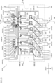
- FIG. 1 is a perspective view of a semiconductor device according to a first embodiment of the present disclosure.
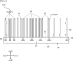
- FIG. 2 is a plan view of the semiconductor device shown in FIG. 1.
- FIG. 3 is a plan view corresponding to FIG. 2, in which the sealing resin is seen through.
- FIG. 4 is a bottom view of the semiconductor device shown in FIG. 1.
- FIG. 5 is a front view of the semiconductor device shown in FIG. 1.
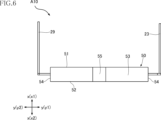
- FIG. 6 is a right side view of the semiconductor device shown in FIG. 1.
- FIG. 7 is a sectional view taken along line VII-VII in FIG. 3.
- FIG. 8 is a cross-sectional view taken along line VIII-VIII in FIG. 3.
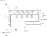
- FIG. 9 is an enlarged plan view of essential parts of the semiconductor device shown in FIG. 1.
- FIG. 1 is a perspective view of a semiconductor device according to a first embodiment of the present disclosure.
- FIG. 2 is a plan view of the semiconductor device shown in FIG. 1.
- FIG. 3 is a plan view corresponding to FIG
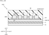
- FIG. 10 is an enlarged sectional view of a main part taken along line XX in FIG. 9.
- FIG. 11 is an enlarged sectional view of a main part taken along line XI-XI in FIG.
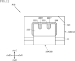
- FIG. 12 is an enlarged plan view of essential parts of the semiconductor device shown in FIG. 1.
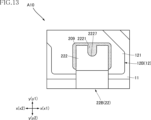
- FIG. 13 is an enlarged plan view of essential parts of the semiconductor device shown in FIG.
- FIG. 14 is an enlarged plan view of essential parts of the semiconductor device shown in FIG. 1.
- FIG. 15 is an enlarged plan view of a main part of a semiconductor device according to a second embodiment of the present disclosure.
- FIG. 16 is an enlarged sectional view of a main part taken along line XVI-XVI in FIG. 15.
- FIG. 17 is an enlarged sectional view of a main part taken along line XVII-XVII in FIG. 15.
- FIG. 18 is an enlarged plan view of a main part of a semiconductor device according to a third embodiment of the present disclosure.
- a thing A is formed on a thing B and "a thing A is formed on a thing B” mean “a thing A is formed on a thing B” unless otherwise specified.
- "something A is placed on something B” and “something A is placed on something B” mean "something A is placed on something B” unless otherwise specified.
- a certain surface A faces (one side or the other side of) the direction B is not limited to the case where the angle of the surface A with respect to the direction B is 90 degrees; Including cases where it is tilted to the opposite direction.
- the semiconductor device A10 of this embodiment includes an insulating layer 11, a plurality of conductive layers 12, a heat dissipation layer 13, a plurality of input leads 21, a plurality of output leads 22, a plurality of semiconductor elements 31, a bonding layer 39, and a plurality of first wires. 41, a plurality of second wires 42, and a sealing resin 50.
- the semiconductor device A10 includes a plurality of control leads 23, a dummy lead 29, a plurality of diodes 32, a plurality of ICs 33, a plurality of diodes 34, a plurality of third wires 43, a plurality of fourth wires 44, and a plurality of fifth wires 45. and a plurality of sixth wires 46.
- the sealing resin 50 is shown.
- the transparent sealing resin 50 is shown by an imaginary line (two-dot chain line).
- first direction z A direction perpendicular to the first direction z is called a "second direction y.”
- a direction perpendicular to the first direction z and the second direction y is referred to as a "third direction x.”
- the first side in the first direction z is called the z1 side, and the opposite second side is called the z2 side.
- the first side in the second direction y is called the y1 side, and the opposite second side is called the y2 side.
- the first side in the third direction x is called the x1 side, and the opposite second side is called the x2 side.
- the semiconductor device A10 converts DC power input to the plurality of input leads 21 into AC power using the plurality of semiconductor elements 31.
- the converted AC power is output from the plurality of output leads 22 as three phases (U phase, V phase, W phase) each having a different phase.
- the semiconductor device A10 is an IPM (Intelligent Power Module).
- the semiconductor device A10 is used, for example, in a power supply circuit for driving a three-phase AC motor.
- the insulating layer 11 supports a plurality of conductive layers 12, as shown in FIGS. 3, 7, and 8.
- the insulating layer 11 is made of ceramics containing aluminum nitride (AlN), for example.
- AlN aluminum nitride
- the insulating layer 11 has a rectangular shape with the third direction x as the long side direction.
- Conductive layer The plurality of conductive layers 12 are bonded to the insulating layer 11, as shown in FIGS. 7 and 8.
- the composition of the plurality of conductive layers 12 includes copper (Cu).
- the plurality of conductive layers 12 are surrounded by the outer edge of the insulating layer 11 when viewed in the first direction z.
- the dimension of each of the plurality of conductive layers 12 in the first direction z is larger than the dimension of the insulating layer 11 in the first direction z.
- each of the plurality of conductive layers 12 has a main surface 121.
- the main surface 121 faces the z1 side in the first direction z.
- the plurality of conductive layers 12 include a first conductive layer 12A and a plurality of second conductive layers 12B.
- the plurality of second conductive layers 12B are located on the x2 side of the first conductive layer 12A in the third direction x.
- Heat dissipation layer As shown in FIGS. 7 and 8, the heat dissipation layer 13 is located on the z2 side in the first direction z, which is the opposite side from the plurality of conductive layers 12 with respect to the insulating layer 11.
- the heat dissipation layer 13 is bonded to the insulating layer 11.
- the composition of the heat dissipation layer 13 includes copper.
- the heat dissipation layer 13 is surrounded by the outer edge of the insulating layer 11 when viewed in the first direction z.
- the dimension of the heat dissipation layer 13 in the first direction z is larger than the dimension of the insulating layer 11 in the first direction z.
- the insulating layer 11, the plurality of conductive layers 12, and the heat dissipation layer 13 are obtained from a DBC (Direct Bonded Copper) substrate.
- the plurality of conductive layers 12 and heat dissipation layer 13 are formed by etching a copper foil that forms part of the DBC board. Note that the conductive layer of the present disclosure is not limited to forming part of the DBC substrate.
- Each of the plurality of semiconductor elements 31 is bonded to one of the main surfaces 121 of the plurality of conductive layers 12, as shown in FIGS. 3 and 7.
- the multiple semiconductor elements 31 include multiple first elements 31A and multiple second elements 31B.
- the plurality of first elements 31A are joined to the main surface 121 of the first conductive layer 12A among the plurality of conductive layers 12.
- the plurality of second elements 31B are individually bonded to the main surface 121 of each of the plurality of second conductive layers 12B among the plurality of conductive layers 12.
- the plurality of semiconductor elements 31 are, for example, MOSFETs (Metal-Oxide-Semiconductor Field-Effect Transistors). In addition, the plurality of semiconductor elements 31 may be switching elements such as IGBTs (Insulated Gate Bipolar Transistors), or diodes. In the description of the semiconductor device A10, the plurality of semiconductor elements 31 are, for example, IGBTs.
- the plurality of semiconductor elements 31 include a compound semiconductor substrate.
- the composition of the compound semiconductor substrate includes silicon carbide (SiC). As shown in FIG. 9, the plurality of semiconductor elements 31 have a first electrode 311, a second electrode 312, and a gate electrode 313.
- the first electrode 311 faces one of the main surfaces 121 of the plurality of conductive layers 12. A current corresponding to the power before being converted by the semiconductor element 31 flows through the first electrode 311 . That is, the first electrode 311 corresponds to the drain electrode of the semiconductor element 31.
- the second electrode 312 is located on the z1 side in the first direction z. A current corresponding to the power converted by the semiconductor element 31 flows through the second electrode 312 . That is, the second electrode 312 corresponds to the source electrode of the semiconductor element 31.
- the second electrode 312 includes multiple metal plating layers.
- the second electrode 312 includes a nickel (Ni) plating layer and a gold (Au) plating layer stacked on the nickel plating layer.
- the second electrode 312 may include a nickel plating layer, a palladium (Pd) plating layer laminated on the nickel plating layer, and a gold plating layer laminated on the palladium plating layer. good.
- the gate electrode 313 is provided on the same z1 side as the second electrode 312 in the first direction z, and is located away from the second electrode 312. A gate voltage for driving the semiconductor element 31 is applied to the gate electrode 313 . As shown in FIG. 10, the area of the gate electrode 313 is smaller than the area of the second electrode 312 when viewed in the first direction z.
- the bonding layer 39 bonds one of the main surfaces 121 of the plurality of conductive layers 12 and one of the plurality of semiconductor elements 31.
- the first electrode 311 of each of the plurality of first elements 31A is conductively bonded to the main surface 121 of the first conductive layer 12A via the bonding layer 39.
- the first electrode 311 of each of the plurality of second elements 31B is individually conductively bonded to the main surface 121 of each of the plurality of second conductive layers 12B via the bonding layer 39.
- Bonding layer 39 is solder.
- Diode 32 The plurality of diodes 32 are bonded to one of the main surfaces 121 of the plurality of conductive layers 12, as shown in FIGS. 3 and 7.
- the multiple diodes 32 include multiple diodes 32A and multiple diodes 32B.
- the plurality of diodes 32A are electrically connected to the main surface 121 of the first conductive layer 12A among the plurality of conductive layers 12, and are arranged on the y2 side in the second direction y with respect to the plurality of first elements 31A. .
- the plurality of diodes 32B are individually electrically connected to the main surface 121 of each of the plurality of second conductive layers 12B among the plurality of conductive layers 12, and are connected to the plurality of second elements 31B in the second direction y2. placed on the side.
- the plurality of semiconductor elements 31 are, for example, MOSFETs having a SiC (silicon carbide) substrate, a configuration without the plurality of diodes 32 may be used.
- the specific configuration of the diode 32 is not limited at all, and includes, for example, an n+ type silicon substrate.
- a cathode electrode and an anode electrode are formed on both sides of the silicon substrate 440.
- the anode electrode and the cathode electrode are made of metal (for example, gold (Au), nickel (Ni), silicide, cobalt (Co) silicide, etc.).
- Input lead 21, output lead 22, control lead 23, dummy lead 29 The plurality of input leads 21, the plurality of output leads 22, the plurality of control leads 23, and the dummy leads 29 are formed using, for example, the same lead frame.
- the lead frame is made of a material containing copper (Cu) or a copper alloy. Therefore, the compositions of the plurality of input leads 21, the plurality of output leads 22, the plurality of control leads 23, and the dummy lead 29 include copper.
- the plurality of input leads 21 include a first input lead 21A and a plurality of second input leads 21B.
- the first input lead 21A is arranged on the x1 side in the third direction x with respect to the second output lead 22B.
- the plurality of second input leads 21B are arranged on the x2 side in the third direction x with respect to the plurality of output leads 22.
- Each of the plurality of input leads 21 has a terminal portion 211 and a connecting portion 212.
- the terminal portion 211 is exposed to the outside from the sealing resin 50.
- the connecting portion 212 is covered with a sealing resin 50.
- the connecting portion 212 of the first input lead 21A is conductively bonded to the main surface 121 of the first conductive layer 12A via a bonding material 209.
- the first input lead 21A corresponds to a P terminal (positive electrode) into which DC power to be converted is input.
- the specific configuration of the bonding material 209 is not limited at all, and in this embodiment, it has electrical conductivity. Examples of the conductive bonding material 209 include solder, silver (Ag) paste, silver (Ag) fired material, and the like. Further, the bonding material of the present disclosure may be insulating. In this case, the input lead 21 and the semiconductor element 31 (and the diode 32) are electrically connected to each other via, for example, a separate wire.
- the connecting portion 212 has one or more first recesses 2121.
- the number of first recesses 2121 is not limited at all, and may be one or two or more.
- the connecting portion 212 has four first recesses 2121.
- the first recess 2121 is open on the z2 side in the first direction z and on the y1 side in the second direction y.
- the first recess 2121 of this embodiment is open on the z1 side in the first direction z. That is, the first recess 2121 penetrates the connecting portion 212 in the first direction z. Further, the first recess 2121 is closed on the y2 side in the second direction y, and closed on both sides in the third direction x.
- the size of the first recess 2121 is not limited at all. In this embodiment, for example, the size of the first recess 2121 in the second direction y is larger than the thickness of the connecting portion 212 in the first direction z.
- the shape of the first recess 2121 is not limited at all.
- the first recess 2121 has a concave curved surface 2127.
- the concave curved surface 2127 is a surface of the first recess 2121 located closest to the y2 side in the second direction y, and is a curved surface concave toward the y2 side in the second direction y.
- the first recess 2121 has a protrusion 201 and a curved surface 202.
- the protrusion 201 is a portion that protrudes toward the z2 side from the edge of the first recess 2121 on the z2 side in the first direction z.
- the curved surface 202 is a convex curved surface located at the edge of the first recess 2121 on the z1 side in the first direction z.
- the protrusion 201 and the curved surface 202 are formed as a result of a punching operation of a mold, for example, when the first recess 2121 is formed by punching.
- the plurality of first recesses 2121 are lined up in the third direction x.
- the connecting portion 212 has a shape whose longitudinal direction is the third direction x when viewed in the first direction z, and is, for example, approximately rectangular.
- the first recess 2121 accommodates a portion of the bonding material 209.
- the bonding material 209 is applied to a region of the first recess 2121 from the end on the z2 side in the first direction z to near the end on the z1 side. Filled. Note that, depending on the amount of the bonding material 209, the entire first recess 2121 may be filled with the bonding material 209. Alternatively, the bonding material 209 may be configured to protrude toward the z1 side of the first recess 2121 in the first direction z. In the illustrated example, the bonding material 209 exists around the connection portion 212 when viewed in the first direction z.
- the plurality of second input leads 21B are separated from the insulating layer 11.
- the plurality of second input leads 21B are supported by the sealing resin 50.
- the plurality of second input leads 21B are separated from the plurality of conductive layers 12 when viewed in the first direction z.
- the plurality of second input leads 21B correspond to an N terminal (negative electrode) into which DC power to be converted is input.
- Output lead 22 As shown in FIG. 3, the plurality of output leads 22 are located between the first input lead 21A and the plurality of second input leads 21B in the third direction x.
- the plurality of output leads 22 include a first output lead 22A, a second output lead 22B, and a third output lead 22C.
- Each of the output leads 22 has a terminal portion 221 and a connection portion 222.
- the terminal portion 221 is exposed to the outside from the sealing resin 50.
- the connecting portion 222 is connected to the terminal portion 221 and covered with the sealing resin 50.
- connection portions 222 of each of the plurality of output leads 22 are individually conductively bonded to the main surface 121 of each of the plurality of second conductive layers 12B via a bonding material 209. Three-phase AC power converted by the plurality of semiconductor elements 31 is output from the plurality of output leads 22 .
- connection portion 222 of the plurality of output leads 22 has one or more first recesses 2221.
- the number of first recesses 2221 is not limited at all, and may be one or two or more.
- the connection portion 222 of the first output lead 22A has two first recesses 2221.
- the connection portion 222 of the second output lead 22B has one first recess 2221.
- the connecting portion 222 of the third output lead 22C has four first recesses 2221.
- the first recess 2221 is open on the z2 side in the first direction z and on the y1 side in the second direction y.
- the first recess 2221 of this embodiment is open on the z1 side in the first direction z. That is, the first recess 2221 penetrates the connecting portion 222 in the first direction z. Further, the first recess 2221 is closed on the y2 side in the second direction y, and closed on both sides in the third direction x.
- the size of the first recess 2221 is not limited at all. In this embodiment, for example, the size of the first recess 2221 in the second direction y is larger than the thickness of the connecting portion 222 in the first direction z.
- the shape of the first recess 2221 is not limited at all.
- the first recess 2221 has a concave curved surface 2227.
- the concave curved surface 2227 is a surface of the first recess 2221 located closest to the y2 side in the second direction y, and is a curved surface concave toward the y2 side in the second direction y.
- a plurality of first recesses 2221 are lined up in the third direction x.
- the connecting portion 222 of the third output lead 22C has a shape whose longitudinal direction is the third direction x when viewed in the first direction z, and is, for example, approximately rectangular.
- the first recess 2221 accommodates a portion of the bonding material 209.
- the relationship between the first recess 2221 and the bonding material 209 is, for example, the same as the relationship between the first recess 2121 and the bonding material 209 described with reference to FIGS. 10 and 11.
- each of the plurality of output leads 22 further includes a pad portion 223.
- the pad portion 223 is located on the y2 side in the second direction y and on the x1 side in the third direction x with respect to the connection portion 222 when viewed in the first direction z. Further, the pad portion 223 is located on the z1 side in the first direction z with respect to the connection portion 222.
- the shape of the pad portion 223 is not limited at all, and in the illustrated example, it is rectangular.
- the first wire 41 is connected to the pad portion 223 .
- Control lead 23 As shown in FIG. 3, the plurality of control leads 23 are located on the y1 side in the second direction y with respect to the plurality of conductive layers 12. The plurality of control leads 23 are located apart from the insulating layer 11 and supported by the sealing resin 50, similarly to the plurality of second input leads 21B. As shown in FIGS. 2 and 4, a portion of each of the plurality of control leads 23 is exposed to the outside from the sealing resin 50.
- the plurality of control leads 23 include a ground lead 231, a plurality of power supply leads 232, a plurality of first control leads 233, a plurality of second control leads 234, and a dummy lead 235.
- a plurality of ICs 33 are mounted on the ground lead 231.
- the ground lead 231 serves as a ground for the plurality of ICs 33.
- the plurality of ICs 33 are located on the y1 side in the second direction y with respect to the plurality of conductive layers 12.
- the plurality of ICs 33 include a first IC 33A and a second IC 33B that are separated from each other in the third direction x.
- the plurality of power supply leads 232 are inputted with a power source that is the basis of the gate voltage for driving the plurality of first elements 31A.
- Electric signals related to control of the first IC 33A are input and output to the plurality of first control leads 233.
- Electric signals related to control of the second IC 33B are input and output to the plurality of second control leads 234.
- the dummy lead 235 is not electrically connected to the plurality of ICs 33.
- the first IC 33A is located closer to the first conductive layer 12A than the second IC 33B.
- the first IC 33A applies a gate voltage to the gate electrodes 313 of the plurality of first elements 31A.
- the second IC 33B applies a gate voltage to the gate electrodes 313 of the plurality of second elements 31B.
- Diode 34 As shown in FIG. 8, the plurality of diodes 34 are individually conductively bonded to the plurality of power supply leads 232 via the bonding layer 39. The plurality of diodes 34 prevent reverse bias from being applied to the plurality of power supply leads 232 as the plurality of first elements 31A are driven.
- Dummy lead 29 As shown in FIG. 3, the dummy lead 29 is separated from the insulating layer 11 when viewed in the first direction z. The dummy lead 29 is located on the x1 side in the third direction x with respect to the first input lead 21A. As shown in FIGS. 2, 4, and 6, a portion of the dummy lead 29 is exposed to the outside from the sealing resin 50.
- First wire 41 As shown in FIG. 3, the plurality of first wires 41 are individually connected to the second electrodes 312 of each of the plurality of first elements 31A, the plurality of diodes 32A, and the connection portions 222 of each of the plurality of output leads 22. conductively bonded to the Thereby, the second electrode 312 of each of the plurality of first elements 31A is individually electrically connected to the plurality of diodes 32A and the plurality of second conductive layers 12B. Furthermore, the first electrode 311 of each of the plurality of second elements 31B is electrically connected to the second electrode 312 of any one of the plurality of first elements 31A.
- the composition of the plurality of first wires 41 includes aluminum (Al). In addition, the composition of the plurality of first wires 41 may include copper.
- Second wire 42 As shown in FIG. 3, the plurality of second wires 42 are individually conductively bonded to the second electrodes 312 of the plurality of second elements 31B, the plurality of diodes 32B, and the plurality of second input leads 21B. ing. Thereby, the second electrode 312 of each of the plurality of second elements 31B is individually electrically connected to the plurality of diodes 32B and the plurality of second input leads 21B.
- the composition of the plurality of second wires 42 includes aluminum. In addition, the composition of the plurality of second wires 42 may include copper.
- a plurality of upper arm circuits are configured by the first conductive layer 12A, the plurality of first elements 31A, and the plurality of first wires 41.
- a plurality of lower arm circuits are configured by the plurality of second conductive layers 12B, the plurality of second elements 31B, the plurality of second wires 42, and the plurality of second input leads 21B. Therefore, the voltage applied to the gate electrode 313 of each of the plurality of first elements 31A is different from the voltage applied to the gate electrode 313 of each of the plurality of second elements 31B. Furthermore, since the semiconductor device A10 includes the plurality of second input leads 21B, the grounds of the plurality of lower arm circuits are individually set in the semiconductor device A10.
- Third wire 43 As shown in FIG. 3, the plurality of third wires 43 are electrically connected to the first IC 33A and the second electrode 312 and gate electrode 313 of each of the plurality of first elements 31A. As a result, a gate voltage is applied from the first IC 33A to the gate electrodes 313 of the plurality of first elements 31A. At the same time, the ground of the gate voltage is set in the first IC 33A.
- the composition of the plurality of third wires 43 includes, for example, gold.
- Fourth wire 44 As shown in FIG. 3, the plurality of fourth wires 44 are electrically connected to the second IC 33B and the gate electrode 313 of each of the plurality of second elements 31B. Thereby, a gate voltage is applied from the second IC 33B to the gate electrodes 313 of the plurality of second elements 31B.
- the composition of the plurality of fourth wires 44 includes, for example, gold.
- the plurality of fifth wires 45 are electrically connected to the first IC 33A, the ground lead 231, the plurality of power leads 232, the plurality of diodes 34, and the plurality of first control leads 233.
- the ground lead 231, the plurality of power supply leads 232, the plurality of diodes 34, and the plurality of first control leads 233 are electrically connected to the first IC 33A.
- the composition of the plurality of fifth wires 45 includes, for example, gold.
- Sixth wire 46 As shown in FIG. 3, the plurality of sixth wires 46 are connected to the second IC 33B, the ground lead 231, and the plurality of second control leads 234. Thereby, the ground lead 231 and the plurality of second control leads 234 are electrically connected to the second IC 33B.
- the composition of the plurality of sixth wires 46 includes, for example, gold.
- the sealing resin 50 connects the plurality of conductive layers 12, the plurality of semiconductor elements 31, the plurality of diodes 32, the plurality of ICs 33, the connection portions 212 of each of the plurality of input leads 21, and The connecting portion 222 of each of the plurality of output leads 22 is covered. Furthermore, the sealing resin 50 covers a portion of each of the plurality of control leads 23 and a portion of the dummy lead 29.
- the sealing resin 50 has electrical insulation properties.
- the sealing resin 50 is made of a material containing, for example, a black epoxy resin. As shown in FIGS. 1 to 8, the sealing resin 50 has a top surface 51, a bottom surface 52, a pair of first side surfaces 53, a pair of second side surfaces 54, and a pair of recessed portions 55.
- the top surface 51 faces the z1 side in the first direction z.
- the bottom surface 52 faces the z2 side in the first direction z. Therefore, the top surface 51 and the bottom surface 52 face oppositely to each other in the first direction z.
- the heat dissipation layer 13 is exposed to the outside from the bottom surface 52.
- the pair of first side surfaces 53 face oppositely to each other in the third direction x.
- a pair of first side surfaces 53 are connected to the top surface 51 and the bottom surface 52.
- the pair of second side surfaces 54 face oppositely to each other in the second direction y.
- a pair of second side surfaces 54 are connected to the top surface 51 and the bottom surface 52. From the second side surface 54 facing the y2 side of the second direction y, the terminal portions 211 of each of the plurality of input leads 21, the terminal portions 221 of each of the plurality of output leads 22, and a part of the dummy lead 29 are exposed. protruding to the outside.
- a portion of each of the plurality of control leads 23 protrudes to the outside from the second side surface 54 facing the y1 side in the second direction y.
- the pair of recessed portions 55 are recessed from the pair of first side surfaces 53 in the third direction x. In the first direction z, the pair of invaginations 55 extend from the top surface 51 to the bottom surface 52.
- the pair of recessed portions 55 ensure a longer creepage distance of the sealing resin 50 from the terminal portion 211 of any one of the plurality of input leads 21 to any one of the plurality of control leads 23. In addition, a longer creepage distance of the sealing resin 50 from any one of the plurality of second input leads 21B to any one of the plurality of control leads 23 is ensured. This is suitable for improving the dielectric strength of the semiconductor device A10.
- the connecting portion 212 is provided with a first recess 2121.
- the bonding material 209 By accommodating a portion of the bonding material 209 in the first recess 2121, it is possible to expand the bonding area between the connecting portion 212 and the bonding material 209. Therefore, the bonding strength of the first input lead 21A can be improved.
- the joining material 209 such as melted solder can be quickly guided into the first recess 2121 when the first input lead 21A is joined. Can be done. Furthermore, since the first recess 2121 is open on the y1 side in the second direction y, when the bonding material 209 such as molten solder is guided into the first recess 2121, it remains in the first recess 2121. It is possible to quickly discharge the air that has been in the air toward the y1 side in the second direction y. Therefore, in the semiconductor device A10, it is possible to suppress the occurrence of unintended air pockets or the like at the joint portion of the connection portion 212.
- the first recess 2121 is open on the z1 side in the first direction z. Thereby, it is possible to increase the amount of bonding material 209 filled in the first recess 2121, and the bonding strength can be further improved. Furthermore, when the bonding material 209 such as molten solder is guided into the first recess 2121, the air stagnant within the first recess 2121 can also be discharged to the z1 side in the first direction z. It is.
- Providing a plurality of first recesses 2121 is preferable for improving the bonding strength of the first input lead 21A.
- the sealing resin 50 has a bottom surface 52 facing opposite to the main surface 121 of the conductive layer 12 in the first direction z.
- the heat dissipation layer 13 is exposed from the bottom surface 52.
- the bonding strength of the output lead 22 can be improved.
- Second embodiment 15 to 17 show a semiconductor device according to a second embodiment of the present disclosure.
- the semiconductor device A20 of this embodiment differs from the above-described embodiments in the configuration of the first recess 2121.
- the first recess 2121 of this embodiment opens on the y1 side in the second direction y and on the z2 side in the first direction z, and closes on the z1 side in the first direction z. That is, the first recess 2121 does not penetrate the connecting portion 212 in the first direction z. When the connecting portion 212 is viewed from the z1 side in the first direction z, the first recess 2121 does not appear in the external appearance of the connecting portion 212.
- the first recess 2121 is entirely filled with the bonding material 209.
- the configuration is not limited to this, and for example, only a portion of the first recess 2121 on the y2 side in the second direction y that connects to the concave curved surface 2127 is filled with the bonding material 209, and the first recess 2121 is filled with the bonding material 209. The portion on the y1 side may not be buried in the bonding material 209.
- the bonding strength of the first input lead 21A can be improved.
- the first recess 2121 is not limited to the configuration in which it penetrates the connecting portion 212 in the first direction z. Further, as shown in FIG. 16, if the first recess 2121 is entirely filled with the bonding material 209 in the zx cross section, the bonding area by the bonding material 209 can be expanded.
- FIG. 18 shows a semiconductor device according to a third embodiment of the present disclosure.
- the semiconductor device A30 of this embodiment is different from the above-described embodiments in the configuration of the connection portion 212.
- the connecting portion 212 of this embodiment has one or more first recesses 2121, one or more second recesses 2122, and one or more third recesses 2123.
- the number of the one or more first recesses 2121 is not limited at all, and in the illustrated example, it is eight.
- the plurality of first recesses 2121 are lined up in the third direction x.
- the first recess 2121 penetrates the connecting portion 212 in the first direction z.
- the second recess 2122 is open on the z2 side in the first direction z and on the y2 side in the second direction y. That is, the second recess 2122 opens on the opposite side of the first recess 2121 in the second direction y.
- the second recess 2122 is closed on the y1 side in the second direction y.
- the second recess 2122 is closed on both sides in the third direction x.
- the plurality of second recesses 2122 are lined up in the third direction x.
- the connecting portion 212 has a shape whose longitudinal direction is the third direction x when viewed in the first direction z, and is, for example, approximately rectangular.
- the third recess 2123 is open on the x1 side or the x2 side in the third direction x, and on the z2 side in the first direction z.
- the plurality of third recesses 2123 are arranged separately on both sides of the connecting portion 212 in the third direction x.
- the third recess 2123 is open on the z1 side in the first direction z.
- the third recess 2123 is closed on both sides in the second direction y.
- the relationship between the second recess 2122 and the third recess 2123 and the bonding material 209 is, for example, the same as the relationship between the first recess 2121 and the bonding material 209 described with reference to FIGS. 10 and 11.
- the bonding strength of the first input lead 21A can be improved.
- the second recess 2122 is provided on the opposite side of the first recess 2121, so that the bonding strength of the first input lead 21A can be further improved.
- the third recess 2123 the bonding strength of the first input lead 21A can be further improved.
- the combination in which the first recess 2121, the second recess 2122, and the third recess 2123 are provided is not limited at all.
- a conductive layer having a main surface facing a first side in a first direction; a semiconductor element bonded to the main surface; a lead having a connecting portion joined to the main surface; a bonding material for bonding the main surface and the connection portion; A sealing resin that covers the semiconductor element,
- the connecting portion has a first recess that accommodates a portion of the bonding material, In the semiconductor device, the first recess is open on a second side in the first direction and a first side in a second direction perpendicular to the first direction.
- Appendix 2 The semiconductor device according to appendix 1, wherein the first recess is closed on a second side in the second direction. Appendix 3.
- the semiconductor device according to appendix 2 wherein the first recess has a concave curved surface located on the second side in the second direction.
- Appendix 4. The semiconductor device according to appendix 2 or 3, wherein the first recess is closed on both sides in a third direction perpendicular to the first direction and the second direction.
- Appendix 5. The semiconductor device according to appendix 4, wherein the first recess is open to the first side in the first direction.
- Appendix 7. 7. The semiconductor device according to appendix 5 or 6, wherein a size of the first recess in the second direction is larger than a thickness of the connecting portion in the first direction.
- the connecting portion has a plurality of the first recesses, 8.
- Appendix 9. The semiconductor device according to appendix 8, wherein the connection portion has a shape whose longitudinal direction is the third direction.
- Appendix 10. 9. The semiconductor device according to any one of appendices 4 to 9, wherein the connection portion has a second recess that opens on a second side in the first direction and a second side in the second direction.
- the semiconductor device according to any one of appendices 4 to 10 wherein the connection portion has a third recess that opens in each of the second side of the first direction and the third direction.
- Appendix 13 The semiconductor element is a switching element, 13.
- Appendix 14. The semiconductor device according to any one of appendices 1 to 13, wherein the bonding material is conductive.
- Appendix 15. 15.
- the semiconductor device according to appendix 15 further comprising a heat dissipation layer bonded to the second side in the first direction with respect to the insulating layer.
- Appendix 17 The semiconductor device according to appendix 16, wherein the heat dissipation layer is exposed from the sealing resin.
Landscapes
- Structures Or Materials For Encapsulating Or Coating Semiconductor Devices Or Solid State Devices (AREA)
Priority Applications (1)
| Application Number | Priority Date | Filing Date | Title |
|---|---|---|---|
| JP2024534970A JPWO2024018795A1 (https=) | 2022-07-21 | 2023-06-16 |
Applications Claiming Priority (2)
| Application Number | Priority Date | Filing Date | Title |
|---|---|---|---|
| JP2022-116213 | 2022-07-21 | ||
| JP2022116213 | 2022-07-21 |
Publications (1)
| Publication Number | Publication Date |
|---|---|
| WO2024018795A1 true WO2024018795A1 (ja) | 2024-01-25 |
Family
ID=89617636
Family Applications (1)
| Application Number | Title | Priority Date | Filing Date |
|---|---|---|---|
| PCT/JP2023/022459 Ceased WO2024018795A1 (ja) | 2022-07-21 | 2023-06-16 | 半導体装置 |
Country Status (2)
| Country | Link |
|---|---|
| JP (1) | JPWO2024018795A1 (https=) |
| WO (1) | WO2024018795A1 (https=) |
Citations (5)
| Publication number | Priority date | Publication date | Assignee | Title |
|---|---|---|---|---|
| JP2000031369A (ja) * | 1998-07-07 | 2000-01-28 | Hitachi Ltd | 半導体装置およびその製造方法 |
| JP2012104708A (ja) * | 2010-11-11 | 2012-05-31 | Shindengen Electric Mfg Co Ltd | 接続板、接合構造及び半導体装置 |
| WO2020075549A1 (ja) * | 2018-10-09 | 2020-04-16 | ローム株式会社 | 半導体装置および半導体装置の製造方法 |
| JP2021101453A (ja) * | 2019-12-24 | 2021-07-08 | 三菱電機株式会社 | 半導体装置およびその製造方法ならびに電力変換装置 |
| JP2021125635A (ja) * | 2020-02-07 | 2021-08-30 | 日立Astemo株式会社 | 半導体装置 |
-
2023
- 2023-06-16 JP JP2024534970A patent/JPWO2024018795A1/ja active Pending
- 2023-06-16 WO PCT/JP2023/022459 patent/WO2024018795A1/ja not_active Ceased
Patent Citations (5)
| Publication number | Priority date | Publication date | Assignee | Title |
|---|---|---|---|---|
| JP2000031369A (ja) * | 1998-07-07 | 2000-01-28 | Hitachi Ltd | 半導体装置およびその製造方法 |
| JP2012104708A (ja) * | 2010-11-11 | 2012-05-31 | Shindengen Electric Mfg Co Ltd | 接続板、接合構造及び半導体装置 |
| WO2020075549A1 (ja) * | 2018-10-09 | 2020-04-16 | ローム株式会社 | 半導体装置および半導体装置の製造方法 |
| JP2021101453A (ja) * | 2019-12-24 | 2021-07-08 | 三菱電機株式会社 | 半導体装置およびその製造方法ならびに電力変換装置 |
| JP2021125635A (ja) * | 2020-02-07 | 2021-08-30 | 日立Astemo株式会社 | 半導体装置 |
Also Published As
| Publication number | Publication date |
|---|---|
| JPWO2024018795A1 (https=) | 2024-01-25 |
Similar Documents
| Publication | Publication Date | Title |
|---|---|---|
| CN102655140B (zh) | 多晶片封装 | |
| JP2024056982A (ja) | 半導体装置 | |
| JP7795476B2 (ja) | 半導体装置 | |
| JP2020077694A (ja) | 半導体装置 | |
| CN110600457A (zh) | 半导体装置 | |
| WO2024116873A1 (ja) | 半導体モジュール | |
| WO2023112662A1 (ja) | 半導体モジュールおよび半導体装置 | |
| US12249570B2 (en) | Semiconductor device | |
| JP2023088628A (ja) | 半導体装置 | |
| JP2022144459A (ja) | 半導体装置 | |
| WO2024018795A1 (ja) | 半導体装置 | |
| WO2023149257A1 (ja) | 半導体装置 | |
| WO2024247629A1 (ja) | 半導体装置および車両 | |
| US20240030080A1 (en) | Semiconductor device | |
| CN119183608A (zh) | 半导体器件 | |
| WO2022070741A1 (ja) | 半導体装置 | |
| WO2021215294A1 (ja) | 半導体装置 | |
| US20260096491A1 (en) | Semiconductor device and vehicle | |
| US20240304589A1 (en) | Semiconductor device | |
| US20250167163A1 (en) | Semiconductor device | |
| WO2023199808A1 (ja) | 半導体装置 | |
| WO2023162700A1 (ja) | 半導体装置 | |
| WO2024106219A1 (ja) | 半導体装置 | |
| WO2024116743A1 (ja) | 半導体装置 | |
| CN117999650A (zh) | 半导体装置 |
Legal Events
| Date | Code | Title | Description |
|---|---|---|---|
| 121 | Ep: the epo has been informed by wipo that ep was designated in this application |
Ref document number: 23842726 Country of ref document: EP Kind code of ref document: A1 |
|
| WWE | Wipo information: entry into national phase |
Ref document number: 2024534970 Country of ref document: JP |
|
| NENP | Non-entry into the national phase |
Ref country code: DE |
|
| 122 | Ep: pct application non-entry in european phase |
Ref document number: 23842726 Country of ref document: EP Kind code of ref document: A1 |