WO2024014118A1 - レベルシフト回路 - Google Patents
レベルシフト回路 Download PDFInfo
- Publication number
- WO2024014118A1 WO2024014118A1 PCT/JP2023/018588 JP2023018588W WO2024014118A1 WO 2024014118 A1 WO2024014118 A1 WO 2024014118A1 JP 2023018588 W JP2023018588 W JP 2023018588W WO 2024014118 A1 WO2024014118 A1 WO 2024014118A1
- Authority
- WO
- WIPO (PCT)
- Prior art keywords
- potential
- output terminal
- level shift
- positive
- negative
- Prior art date
- Legal status (The legal status is an assumption and is not a legal conclusion. Google has not performed a legal analysis and makes no representation as to the accuracy of the status listed.)
- Ceased
Links
Images








Classifications
-
- H—ELECTRICITY
- H03—ELECTRONIC CIRCUITRY
- H03K—PULSE TECHNIQUE
- H03K19/00—Logic circuits, i.e. having at least two inputs acting on one output; Inverting circuits
- H03K19/0175—Coupling arrangements; Interface arrangements
Definitions
- the present technology relates to a level shift circuit. Specifically, the present technology relates to a level shift circuit in which a positive DC voltage and a negative DC voltage are used.
- level shift circuits are sometimes used to convert the level of signals.
- a level shift circuit for example, when converting the level of a signal from a first potential to a second potential, a power supply with an intermediate potential between the first potential and the second potential is provided, and once the signal is converted to an intermediate level signal, the potential difference is reduced.
- a technique has been proposed in which conversion is repeatedly performed in a natural manner (for example, see Patent Document 1).
- This technology was created in view of this situation, and its purpose is to speed up level shifting using positive DC voltage and negative DC voltage.
- the present technology has been developed to solve the above-mentioned problems, and its first aspect is a level shift unit that level-shifts a signal from a first potential to a second potential and outputs it via an output terminal.
- a current path setting section that sets a second current path separate from the first current path from the level shift section to the output terminal to the output terminal; and a current path setting section that opens and closes the first current path and the second current path.
- This is a level shift circuit comprising an opening/closing section. This brings about the effect that restrictions on the impedance of charging and discharging the load at the time of level shifting are alleviated.
- the current path setting unit sets the second current path so that the potential of the output terminal approaches the second potential when the output terminal is disconnected from the second potential. It may be set to the above output terminal. This brings about the effect that the amount of charge charged and discharged in the load when the output terminal is switched to the second potential is reduced.
- the second current path includes at least one of a discharging path through which electric charges are discharged via the output terminal and a charging path through which electric charges are charged through the output terminal. But that's fine. This brings about the effect that the second current path used for charging and discharging the load is secured separately from the first current path when the output terminal is switched to the second potential.
- the second potential includes a positive DC potential and a negative DC potential
- the level shift section changes the first potential to the positive DC potential or the negative DC potential. It may be selectively converted and outputted via the output terminal. This brings about the effect that the signal at the first potential is level-shifted to a positive DC potential or a negative DC potential.
- the level shift section includes a first switching element that connects the positive DC potential to the output terminal, and a second switching element that connects the negative DC potential to the output terminal. You may prepare. This brings about the effect that the signal at the first potential is selectively converted into a positive DC potential or a negative DC potential.
- the current path setting section may include a third switching element that connects the output terminal to a third potential. This provides the effect of ensuring a current path used for charging and discharging the load.
- the third potential may be a ground potential, a power supply potential, or an intermediate potential between the positive DC potential and the negative DC potential. This brings about the effect that the load is charged and discharged without intervening the level shift section.
- the switching unit connects the output terminal to the positive DC potential, disconnects the output terminal from the positive DC potential, and then connects the output terminal to the ground potential. , after disconnecting the output terminal from the ground potential, the output terminal may be connected to the negative DC potential. This brings about the effect that the load is discharged before the potential of the output terminal is switched from a positive DC potential to a negative DC potential.
- the switching section connects the output terminal to the positive DC potential, disconnects the output terminal from the positive DC potential, and then connects the output terminal to the intermediate potential. , after disconnecting the output terminal from the intermediate potential, the output terminal may be connected to the negative DC potential. This brings about the effect that the load is discharged so as to approach the negative DC potential before the potential of the output terminal is switched from the positive DC potential to the negative DC potential.
- the switching unit connects the output terminal to the negative DC potential, disconnects the output terminal from the negative DC potential, and then connects the output terminal to the power supply potential. , after disconnecting the output terminal from the power supply potential, the output terminal may be connected to the positive DC potential. This brings about the effect that the load is charged before the potential of the output terminal is switched from a negative DC potential to a positive DC potential.
- the switching unit connects the output terminal to the negative DC potential, disconnects the output terminal from the negative DC potential, and then connects the output terminal to the intermediate potential. , after disconnecting the output terminal from the intermediate potential, the output terminal may be connected to the positive DC potential. This brings about the effect that before the potential of the output terminal is switched from a negative DC potential to a positive DC potential, the load is charged so that it approaches the positive DC potential.
- the current path setting section may include a fourth switching element that connects the output terminal to a fourth potential. This brings about the effect that the current path used for discharging the load and the current path used for charging the load are secured separately.
- the third potential may be a ground potential
- the fourth potential may be a power supply potential. This brings about the effect that the load is charged and discharged via a current path that does not involve a level shift section.
- the third potential is a positive intermediate potential between the positive DC potential and the negative DC potential
- the fourth potential is a positive intermediate potential between the positive DC potential and the negative DC potential. It may be a negative intermediate potential between. This brings about the effect that the load is charged and discharged via a current path that does not involve a level shift section so as to approach a positive DC potential or a negative DC potential.
- the first aspect may further include a delay circuit that delays connection of the second potential to the output terminal when the signal is level-shifted from the first potential to the second potential. good. This provides the effect of ensuring time for the load to be charged and discharged before the signal is level-shifted from the first potential to the second potential.
- the switching unit is configured to open the first current path and close the second current path when connection of the second potential to the output terminal is delayed. You can also use it as This brings about the effect that the load is charged and discharged before the level of the signal is shifted from the first potential to the second potential.
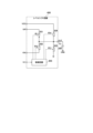
- FIG. 2 is a block diagram showing an example of the functional configuration of a level shift circuit according to the first embodiment.
- FIG. 3 is a diagram showing an example of the load of the level shift circuit according to the first embodiment.
- 1 is a diagram showing an example of a circuit configuration of a level shift circuit according to a first embodiment;
- FIG. 7 is a timing chart showing a first operation example of the level shift circuit according to the first embodiment.
- FIG. FIG. 3 is a diagram showing a current path based on a first example of level shift operation according to the first embodiment.
- FIG. 3 is a diagram showing a current path based on a first example of level shift operation according to the first embodiment.
- FIG. 3 is a diagram showing a current path based on a first example of level shift operation according to the first embodiment.
- FIG. 7 is a diagram showing a waveform when a gate voltage falls based on a level shift operation according to the first embodiment.
- 7 is a timing chart showing a second operation example of the level shift circuit according to the first embodiment.
- FIG. 7 is a diagram showing a current path based on a second example of level shift operation according to the first embodiment.
- FIG. 7 is a diagram showing a current path based on a second example of level shift operation according to the first embodiment.
- FIG. 7 is a diagram showing a current path based on a second example of level shift operation according to the first embodiment.
- FIG. 6 is a diagram showing a waveform at the time of rise of a gate voltage based on a level shift operation according to the first embodiment.
- FIG. 1 is a diagram showing an example of a circuit configuration of a level shift circuit according to a first embodiment
- FIG. FIG. 3 is a diagram showing the relationship between the discharge time and the output switching time of the level shift circuit according to the first embodiment.
- FIG. 7 is a diagram showing an example of a circuit configuration of a level shift circuit according to a second embodiment.
- FIG. 7 is a diagram showing an example of a circuit configuration of a level shift circuit according to a third embodiment.
- FIG. 7 is a diagram showing an example of a circuit configuration of a level shift circuit according to a fourth embodiment.
- First embodiment (example in which a charging/discharging path is provided at ground potential) 2.
- Second embodiment (example in which a charging/discharging path is provided in the power supply potential) 3.
- Third embodiment (example in which charging and discharging paths are provided for ground potential and power supply potential) 4.
- Fourth embodiment (example in which a charging/discharging path is provided at an intermediate potential between a positive DC potential and a negative DC potential)
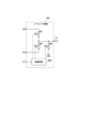
- FIG. 1 is a block diagram showing an example of the functional configuration of a level shift circuit according to the first embodiment.
- the level shift circuit 100 sets a second current path separate from the first current path used for signal level shifting, charges and discharges charges via the second current path, and then The signal level is shifted through one current path. Note that when it is referred to as charging and discharging in this specification, it is not necessarily necessary to perform both charging and discharging, and only charging or discharging may be performed.
- the level shift circuit 100 includes a level shift section 101, an input/output switching section 102, and a charging/discharging section 103.
- the level shift unit 101 level-shifts the digital signal VC from the first potential to the second potential and outputs the level-shifted signal VC.
- the second potential may include a positive DC potential VIP and a negative DC potential VIN.
- the level shift unit 101 can selectively convert the digital signal VC at the first potential into a positive DC potential VIP or a negative DC potential VIN and output the converted signal.
- the input/output switching unit 102 opens and closes the path between the output of the level shift unit 101 and the input of the charging/discharging unit 103 based on the control signals ⁇ 1 and ⁇ 2.
- the control signal ⁇ 1 controls the level shift to the positive DC potential VIP
- the control signal ⁇ 2 controls the level shift to the negative DC potential VIN.
- the charging/discharging current flowing to the output OUT via the charging/discharging unit 103 is cut off, and the output OUT is a positive DC current. It is selectively connected to potential VIP or negative DC potential VIN.
- the charging/discharging unit 103 sets a second current path that is separate from the first current path used for level shifting of the signal.
- the charging/discharging unit 103 may set the second current path to the output terminal so that the potential of the output terminal approaches the second potential when the output terminal of the level shift circuit 100 is separated from the two potentials.
- the second current path may be a discharge path where charges are discharged via the output terminal of the level shift circuit 100, or a charging path where charges are charged via the output terminal of the level shift circuit 100.
- the charging/discharging unit 103 may connect the output terminal of the level shift circuit 100 to the third potential.
- the third potential may be a ground potential, a power supply potential, or an intermediate potential between a positive DC potential and a negative DC potential.
- the input/output opening/closing unit 102 is an example of an opening/closing unit that opens and closes the first current path described in the claims.
- the charging/discharging unit 103 is an example of a current path setting unit and an opening/closing unit that opens and closes the second current path described in the claims.
- FIG. 2 is a diagram showing an example of the load of the level shift circuit according to the first embodiment.
- an NMOS transistor 110 is provided as a load of the level shift circuit 100.
- the output terminal TO of the level shift circuit 100 is connected to the gate of the NMOS transistor 110.
- the level shift circuit 100 controls the gate voltage of the NMOS transistor 110 based on the output OUT from the output terminal TO.
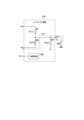
- FIG. 3 is a diagram showing an example of the circuit configuration of the level shift circuit according to the first embodiment.
- a level shift circuit 100 includes switching elements 201 to 203 and a control circuit 205. Note that each of the switching elements 201 to 203 may be a MOS transistor.
- the switching element 201 connects the positive DC potential VIP to the output terminal TO based on the control signal ⁇ 1.
- the switching element 202 connects the negative DC potential VIN to the output terminal TO based on the control signal ⁇ 2.
- Switching element 203 connects output terminal TO to ground potential GND based on control signal ⁇ 3.
- the control circuit 205 generates control signals ⁇ 1 to ⁇ 3 based on the digital signal VC, and outputs them to each of the switching elements 201 to 203.
- control circuit 205 converts the level of the digital signal VC to the positive DC potential VIP when the output OUT is at the negative DC potential VIN.
- the control circuit 205 turns on the switching element 201 with a delay from the input timing of the digital signal VC, and connects the positive DC potential VIP to the output terminal TO.
- the control circuit 205 turns on the switching element 203 and connects the output terminal TO to the ground potential GND, thereby charging the battery through the output terminal TO.
- the control circuit 205 converts the level of the digital signal VC to the negative DC potential VIN when the output OUT is at the positive DC potential VIP. At this time, the control circuit 205 turns on the switching element 202 with a delay from the input timing of the digital signal VC, and connects the negative DC potential VIN to the output terminal TO.
- the control circuit 205 turns on the switching element 203 and connects the output terminal TO to the ground potential GND, thereby causing discharge through the output terminal TO.
- the switching elements 201 and 202 are examples of a level shift unit and an opening/closing unit that opens and closes the first current path described in the claims.
- the switching element 203 is an example of a current path setting section and an opening/closing section that opens and closes the second current path described in the claims.
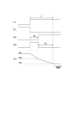
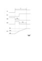
- FIG. 4 is a timing chart showing a first operation example of the level shift circuit according to the first embodiment
- FIGS. 5 to 7 show a first example of the level shift operation according to the first embodiment.
- This capacitive load 206 is, for example, the gate capacitance of the NMOS transistor 110 in FIG.
- the control circuit 205 transitions the control signal ⁇ 1 from high level to low level to turn off the switching element 201, and transitions the control signal ⁇ 3 from low level to high level to turn on the switching element 203.
- the switching element 203 is turned on, as shown in FIG. 6, the output terminal TO is connected to the ground potential GND, and a current LN2 flows from the capacitive load 206 to the ground potential GND. Then, the electric charge accumulated in the capacitive load 206 is discharged to the ground potential GND, so that the potential of the output terminal TO decreases.
- the control circuit 205 transitions the control signal ⁇ 3 from high level to low level to turn off the switching element 203, and transitions the control signal ⁇ 2 from low level to high level, causing the switching element to switch off.
- 202 is turned on.
- the switching element 202 is turned on, as shown in FIG. 7, the output terminal TO is connected to the negative DC potential VIN, and a current LN3 flows from the capacitive load 206 to the negative DC potential VIN. Then, the electric charge accumulated in the capacitive load 206 is discharged to the negative DC potential VIN, so that the potential of the output terminal TO decreases.
- the potential of the output terminal TO is set to the negative DC potential VIN.
- the switching time T for switching the potential of the output OUT from the positive DC potential VIP to the negative DC potential VIN can be given by TC+TD.
- FIG. 8 is a diagram showing a waveform when the gate voltage falls based on the level shift operation according to the first embodiment.
- the waveform WN1 of the output OUT is such that when switching the potential of the output OUT from the positive DC potential VIP to the negative DC potential VIN, the charge accumulated in the capacitive load 206 is discharged to the ground potential GND. is shown by a solid line.
- a dotted line indicates a waveform WN2 of the output OUT that prevents the charge accumulated in the capacitive load 206 from being discharged to the ground potential GND when switching the potential of the output OUT from the positive DC potential VIP to the negative DC potential VIN.
- the switching time T with discharge to the ground potential GND is longer than the switching time T' with no discharge to the ground potential GND. It also becomes shorter, allowing for faster level shifting.
- FIG. 9 is a timing chart showing a second operation example of the level shift circuit according to the first embodiment
- FIGS. 10 to 12 are timing charts showing a first example of the level shift operation according to the first embodiment.
- the control circuit 205 transitions the control signal ⁇ 2 from high level to low level to turn off the switching element 202, and transitions the control signal ⁇ 3 from low level to high level to turn on the switching element 203.
- the switching element 203 is turned on, the output terminal TO is connected to the ground potential GND, and a current LP2 flows from the ground potential GND to the capacitive load 206, as shown in FIG. Then, as the capacitive load 206 is charged from the ground potential GND, the potential of the output terminal TO increases.
- the control circuit 205 transitions the control signal ⁇ 3 from high level to low level to turn off the switching element 203, and transitions the control signal ⁇ 1 from low level to high level, causing the switching element to switch off.
- Turn on 201 When the switching element 201 is turned on, as shown in FIG. 12, the output terminal TO is connected to the positive DC potential VIP, and a current LP3 flows from the positive DC potential VIP to the capacitive load 206. Then, by charging the capacitive load 206 from the positive DC potential VIP, the potential of the output terminal TO increases. Then, after the setup time TC has elapsed, the potential of the output terminal TO is set to the positive DC potential VIP. At this time, the switching time T for switching the potential of the output OUT from the negative DC potential VIN to the positive DC potential VIP can be given by TC+TD.
- FIG. 13 is a diagram showing the waveform at the time of rise of the gate voltage based on the level shift operation according to the first embodiment.
- the waveform WP1 of the output OUT which causes the capacitive load 206 to be charged from the ground potential GND when switching the potential of the output OUT from the negative DC potential VIN to the positive DC potential VIP, is shown by a solid line.
- a waveform WP2 of the output OUT in which the capacitive load 206 is not charged from the ground potential GND when switching the potential of the output OUT from the negative DC potential VIN to the positive DC potential VIP is shown by a dotted line.
- the capacitive load 206 is not charged from the ground potential GND when switching the potential of the output OUT from the negative DC potential VIN to the positive DC potential VIP. At this time, the capacitive load 206 is charged via the level shift section 101 in FIG. Limited by impedance.
- the capacitive load 206 is charged from the ground potential GND. At this time, the capacitive load 206 is charged without going through the level shift unit 101 of FIG. 1 until the delay time TD has elapsed. Therefore, until the delay time TD elapses, charging of the capacitive load 206 is not restricted by the impedance of the level shift section 101.
- the switching time T with charging from the ground potential GND is longer than the switching time T' with no charging from the ground potential GND. It also becomes shorter, allowing for faster level shifting.
- FIG. 14 is a diagram showing an example of the circuit configuration of the level shift circuit according to the first embodiment.
- the switching element 201 includes a PMOS transistor 281.
- Switching element 202 includes an NMOS transistor 282.
- the switching element 203 includes an NMOS transistor 283.
- the control circuit 205 includes a delay circuit 211, an exclusive OR circuit 212, an OR circuit 213, an AND circuit 217, and inverters 214 to 216, 218, and 219. Further, the control circuit 205 includes PMOS transistors 221, 222, 241, 242, 261, and 262, and NMOS transistors 231, 232, 251, 252, 271, and 272.
- the PMOS transistor 221 and the NMOS transistor 231 are connected in series with each other.
- PMOS transistor 222 and NMOS transistor 232 are connected in series with each other.
- PMOS transistor 241 and NMOS transistor 251 are connected in series with each other.
- PMOS transistor 242 and NMOS transistor 252 are connected in series with each other.
- PMOS transistor 261 and NMOS transistor 271 are connected in series with each other.
- PMOS transistor 262 and NMOS transistor 272 are connected in series with each other.
- PMOS transistor 281 and NMOS transistor 282 are connected in series with each other.
- the power supply terminal TVD supplies a power supply for the exclusive OR circuit 212, a power supply for the OR circuit 213, a power supply for the AND circuit 217, a power supply for each inverter 214 to 216, 218, and 219, and each PMOS transistor 221, 222. connected to the source.
- a power supply voltage VDD is supplied to the power supply terminal TVD.
- the signal input terminal TVC is connected to an input of the delay circuit 211, one input of the exclusive OR circuit 212, one input of the OR circuit 213, and one input of the AND circuit 217.
- a digital signal VC is input to the signal input terminal TVC.
- the positive DC terminal TIP is connected to the sources of each PMOS transistor 241, 242, 261 and 281.
- a positive DC potential VIP is supplied to the positive DC terminal TIP.
- the negative DC terminal TIN is connected to the sources of each NMOS transistor 231, 232, 272, and 282.
- a negative DC potential VIN is supplied to the negative DC terminal TIN.
- the output of the delay circuit 211 is connected to the other input of the exclusive OR circuit 212.
- the output of the exclusive OR circuit 212 is connected to the other input of the OR circuit 213, the input of the inverter 214, and the gate of the NMOS transistor 283.
- the output of inverter 214 is connected to the other input of AND circuit 217.
- the output of OR circuit 213 is connected to the input of inverter 215, and the output of inverter 215 is connected to the input of inverter 216 and the gate of PMOS transistor 222.
- the output of AND circuit 217 is connected to the input of inverter 218, and the output of inverter 218 is connected to the input of inverter 219 and the gate of NMOS transistor 252.
- the gate of the PMOS transistor 241 is connected to the drain of the PMOS transistor 242, and the gate of the PMOS transistor 242 is connected to the drain of the PMOS transistor 241. Further, the drain of the PMOS transistor 242 is connected to the gate of the PMOS transistor 261 and the gate of the NMOS transistor 271. Further, the drain of the NMOS transistor 271 is connected to the gate of the PMOS transistor 281, and the source of the NMOS transistor 271 is connected to the source of the PMOS transistor 262. The source of each NMOS transistor 251 and 252 is connected to the source of NMOS transistor 283. The source of the NMOS transistor 283 is connected to the ground potential GND, and the drain of the NMOS transistor 283 is connected to the output terminal TO.
- the gate of the NMOS transistor 231 is connected to the drain of the NMOS transistor 232, and the gate of the NMOS transistor 232 is connected to the drain of the NMOS transistor 231. Further, the drain of the NMOS transistor 232 is connected to the gate of the PMOS transistor 262 and the gate of the NMOS transistor 272. The drain of NMOS transistor 272 is connected to the gate of NMOS transistor 282.
- control circuit 205 generates control signals ⁇ 1 to ⁇ 3 based on the digital signal VC. Then, the control circuit 205 outputs the control signal ⁇ 1 to the gate of the PMOS transistor 281, the control signal ⁇ 2 to the gate of the NMOS transistor 282, and the control signal ⁇ 3 to the gate of the NMOS transistor 283. At this time, the control circuit 205 can generate control signals ⁇ 1 to ⁇ 3 according to the timing shown in FIG.
- the delay circuit 211 can set the delay time TD.
- FIG. 15 is a diagram showing the relationship between the discharge time and the output switching time of the level shift circuit according to the first embodiment. Note that this relationship was obtained through simulation using the level shift circuit shown in FIG.
- the discharge time is equal to the delay time TD in FIG.
- the switching time T' of the output OUT was 27 ⁇ sec.
- the switching time T of the output OUT tended to become shorter. For example, when the discharge time is 10 ⁇ sec, the output OUT switching time T is 19 ⁇ sec, which is 30% shorter than the output OUT switching time T′ when the discharge time is 0 ⁇ sec.
- the level shift circuit 100 sets the output terminal TO to the ground potential GND when performing level conversion between the negative DC potential VIN and the positive DC potential VIP.
- a current path via the output terminal TO is provided to the ground potential GND. This makes it possible to reduce restrictions on the impedance of charging and discharging the capacitive load 206 during level shifting, and to speed up level shifting.
- Second embodiment> when performing level conversion between the negative DC potential VIN and the positive DC potential VIP, the output terminal TO is connected to the ground potential GND, and the current through the output terminal TO is A path was provided to the ground potential GND.
- the output terminal TO when performing level conversion between a negative DC potential VIN and a positive DC potential VIP, the output terminal TO is connected to the power supply potential VDD, and a current path is established via the output terminal TO. is set at the power supply potential VDD.
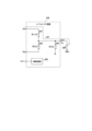
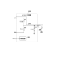
- FIG. 16 is a diagram showing an example of a circuit configuration of a level shift circuit according to the second embodiment.
- a level shift circuit 300 includes a switching element 204 in place of the switching element 203 of the first embodiment described above.
- the rest of the configuration of the level shift circuit 300 of the second embodiment is similar to the configuration of the level shift circuit 100 of the first embodiment described above.
- the switching element 204 connects the output terminal TO to the power supply potential VDD based on the control signal ⁇ 4.
- Power supply potential VDD may be set between ground potential GND and positive DC potential VIP, or may be higher than positive DC potential VIP.
- power supply potential VDD is set between ground potential GND and positive DC potential VIP.
- the control circuit 205 converts the level of the digital signal VC to the positive DC potential VIP when the output OUT is at the negative DC potential VIN.
- the control circuit 205 turns on the switching element 201 with a delay from the input timing of the digital signal VC, and connects the positive DC potential VIP to the output terminal TO.
- the control circuit 205 turns on the switching element 204 and connects the output terminal TO to the power supply potential VDD, thereby charging the battery through the output terminal TO.
- control circuit 205 converts the level of the digital signal VC to the negative DC potential VIN when the output OUT is at the positive DC potential VIP. At this time, the control circuit 205 turns on the switching element 202 with a delay from the input timing of the digital signal VC, and connects the negative DC potential VIN to the output terminal TO.
- the control circuit 205 turns on the switching element 204 and connects the output terminal TO to the power supply potential VDD, thereby causing discharge through the output terminal TO.
- the output terminal TO may be connected to the power supply potential VDD and only charging may be performed via the output terminal TO.
- the level shift circuit 300 sets the output terminal TO to the power supply potential VDD when performing level conversion between the negative DC potential VIN and the positive DC potential VIP.
- a current path is provided to the power supply potential VDD via the output terminal TO. This makes it possible to reduce restrictions on the impedance of charging and discharging the capacitive load 206 during level shifting, and to speed up level shifting.
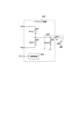
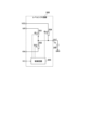
- FIG. 17 is a diagram showing an example of the circuit configuration of a level shift circuit according to the third embodiment.
- a level shift circuit 400 has the switching element 204 of the second embodiment described above added to the level shift circuit 100 of the first embodiment described above.
- the other configuration of the level shift circuit 400 of the third embodiment is the same as the configuration of the level shift circuit 100 of the first embodiment described above.
- control circuit 205 converts the level of the digital signal VC to the positive DC potential VIP when the output OUT is at the negative DC potential VIN. At this time, the control circuit 205 turns on the switching element 201 with a delay from the input timing of the digital signal VC, and connects the positive DC potential VIP to the output terminal TO. Here, before turning on the switching element 201, the control circuit 205 turns on the switching element 204 and connects the output terminal TO to the power supply potential VDD, thereby charging the battery through the output terminal TO.
- the control circuit 205 converts the level of the digital signal VC to the negative DC potential VIN when the output OUT is at the positive DC potential VIP. At this time, the control circuit 205 turns on the switching element 202 with a delay from the input timing of the digital signal VC, and connects the negative DC potential VIN to the output terminal TO.
- the control circuit 205 turns on the switching element 203 and connects the output terminal TO to the ground potential GND, thereby causing discharge through the output terminal TO.
- the power supply potential VDD connected to the charging path can be made higher than the ground potential GND connected to the discharging path. Therefore, when converting the level from the negative DC potential VIN to the positive DC potential VIP, charging via the output terminal TO can be accelerated, and level shifting can be accelerated.
- FIG. 18 is a diagram showing an example of the circuit configuration of a level shift circuit according to the fourth embodiment.
- a level shift circuit 500 can be configured similarly to the level shift circuit 400 of the third embodiment described above.
- the switching element 203 connects the output terminal TO to the intermediate potential VM2 based on the control signal ⁇ 3.
- the switching element 204 connects the output terminal TO to the intermediate potential VM1 based on the control signal ⁇ 4.
- the intermediate potentials VM1 and VM2 can satisfy the relationship VIN ⁇ VM2 ⁇ VM1 ⁇ VIP.
- the intermediate potential VM1 may be a positive intermediate potential between the positive DC potential VIP and the negative DC potential VIN
- the intermediate potential VM2 may be a positive intermediate potential between the positive DC potential VIP and the negative DC potential VIN. It may be an intermediate potential.
- the intermediate potential VM1 is preferably set to a value close to the positive DC potential VIP
- the intermediate potential VM2 is preferably set to a value close to the negative DC potential VIN.
- control circuit 205 converts the level of the digital signal VC to the positive DC potential VIP when the output OUT is at the negative DC potential VIN. At this time, the control circuit 205 turns on the switching element 201 with a delay from the input timing of the digital signal VC, and connects the positive DC potential VIP to the output terminal TO. Here, before turning on the switching element 201, the control circuit 205 turns on the switching element 204 and connects the output terminal TO to the intermediate potential VM1, thereby charging the battery through the output terminal TO.
- the control circuit 205 converts the level of the digital signal VC to the negative DC potential VIN when the output OUT is at the positive DC potential VIP. At this time, the control circuit 205 turns on the switching element 202 with a delay from the input timing of the digital signal VC, and connects the negative DC potential VIN to the output terminal TO.
- the control circuit 205 turns on the switching element 203 and connects the output terminal TO to the intermediate potential VM2, thereby causing discharge through the output terminal TO.
- the intermediate potential VM1 connected to the charging path is made close to the positive DC potential VIP
- the intermediate potential VM2 connected to the discharging path is made close to the negative DC potential VIN. can do. Therefore, when converting the level between the negative DC potential VIN and the positive DC potential VIP, charging and discharging via the output terminal TO can be accelerated, and level shifting can be accelerated.
- the level shift circuit described above may be applied to, for example, a communication IC (Integrated Circuit), an inverter used to drive a motor, etc., or a semiconductor integrated circuit in which multiple power sources are mixed. May be applied to
- the embodiments described above are examples for embodying the present technology, and the matters in the embodiments and the matters specifying the invention in the claims have a corresponding relationship, respectively.
- the matters specifying the invention in the claims and the matters in the embodiments of the present technology having the same names have a corresponding relationship.
- the present technology is not limited to the embodiments, and can be realized by making various modifications to the embodiments without departing from the gist thereof. Further, the effects described in this specification are merely examples and are not limited, and other effects may also be present.
- the present technology can also have the following configuration.
- a level shift unit that level-shifts a signal from a first potential to a second potential and outputs it via an output terminal;
- a current path setting unit that sets a second current path separate from a first current path from the level shift unit to the output terminal to the output terminal;
- a level shift circuit comprising an opening/closing section that opens and closes the first current path and the second current path.
- the current path setting unit sets the second current path to the output terminal so that the potential of the output terminal approaches the second potential when the output terminal is disconnected from the second potential.
- the second current path includes at least one of a discharging path through which electric charges are discharged via the output terminal and a charging path through which electric charges are charged through the output terminal (1) or The level shift circuit according to (2).
- the second potential includes a positive DC potential and a negative DC potential, According to any one of (1) to (3), the level shift unit selectively converts the first potential into the positive DC potential or the negative DC potential and outputs the same through the output terminal. level shift circuit.
- the level shift section includes: a first switching element that connects the positive DC potential to the output terminal; The level shift circuit according to (4), further comprising a second switching element that connects the negative DC potential to the output terminal.
- the current path setting section includes: The level shift circuit according to (5) above, including a third switching element that connects the output terminal to a third potential.
- the level shift circuit according to (6) wherein the third potential is a ground potential, a power supply potential, or an intermediate potential between the positive DC potential and the negative DC potential.
- the opening/closing unit connects the output terminal to the positive DC potential, disconnects the output terminal from the positive DC potential, and then connects the output terminal to the ground potential, and connects the output terminal to the ground potential.
- the opening/closing unit connects the output terminal to the positive DC potential, disconnects the output terminal from the positive DC potential, and then connects the output terminal to the intermediate potential, and connects the output terminal to the intermediate potential.
- the switching unit connects the output terminal to the negative DC potential, disconnects the output terminal from the negative DC potential, and then connects the output terminal to the power supply potential, and connects the output terminal to the power supply potential.
- the opening/closing unit connects the output terminal to the negative DC potential, disconnects the output terminal from the negative DC potential, and then connects the output terminal to the intermediate potential, and connects the output terminal to the intermediate potential.
- the current path setting section includes: The level shift circuit according to any one of (6) to (11), including a fourth switching element that connects the output terminal to a fourth potential.
- the third potential is a positive intermediate potential between the positive DC potential and the negative DC potential
- the fourth potential is a negative intermediate potential between the positive DC potential and the negative DC potential.
- the level shift circuit according to (12) above which has an intermediate potential.
- the opening/closing unit is configured to open the first current path and close the second current path when connection of the second potential to the output terminal is delayed. ) level shift described
- Level shift circuit 100, 300, 400, 500 Level shift circuit 101 Level shift section 102 Input/output switching section 103 Charging/discharging section 201 to 204 Switching element 205 Control circuit 206 Capacitive load
Landscapes
- Engineering & Computer Science (AREA)
- Computer Hardware Design (AREA)
- Physics & Mathematics (AREA)
- Computing Systems (AREA)
- General Engineering & Computer Science (AREA)
- Mathematical Physics (AREA)
- Logic Circuits (AREA)
Abstract
Description
1.第1の実施の形態(接地電位に充放電経路を設けた例)
2.第2の実施の形態(電源電位に充放電経路を設けた例)
3.第3の実施の形態(接地電位および電源電位に充放電経路を設けた例)
4.第4の実施の形態(正の直流電位と負の直流電位との間の中間電位に充放電経路を設けた例)
図1は、第1の実施の形態に係るレベルシフト回路の機能構成例を示すブロック図である。
上述の第1の実施の形態では、負の直流電位VINと正の直流電位VIPとの間でレベル変換を行うときに、出力端子TOを接地電位GNDに接続し、出力端子TOを介した電流経路を接地電位GNDに設けた。この第2の実施の形態では、負の直流電位VINと正の直流電位VIPとの間でレベル変換を行うときに、出力端子TOを電源電位VDDに接続し、出力端子TOを介した電流経路を電源電位VDDに設ける。
上述の第1の実施の形態では、負の直流電位VINと正の直流電位VIPとの間でレベル変換を行うときに、出力端子TOを接地電位GNDに接続し、出力端子TOを介した電流経路を接地電位GNDに設けた。この第3の実施の形態では、負の直流電位VINと正の直流電位VIPとの間でレベル変換を行うときに、出力端子TOを介した電流経路を接地電位GNDおよび電源電位VDDに設ける。
上述の第1の実施の形態では、負の直流電位VINと正の直流電位VIPとの間でレベル変換を行うときに、出力端子TOを介した電流経路を接地電位GNDおよび電源電位VDDに設けた。この第4の実施の形態では、負の直流電位VINと正の直流電位VIPとの間でレベル変換を行うときに、出力端子TOを介した電流経路を負の直流電位VINと正の直流電位VIPとの間の中間電位に設ける。
(1)第1電位から第2電位へ信号をレベルシフトし、出力端子を介して出力するレベルシフト部と、
前記レベルシフト部から前記出力端子までの第1電流経路と別個の第2電流経路を前記出力端子に設定する電流経路設定部と、
前記第1電流経路および前記第2電流経路を開閉する開閉部と
を具備するレベルシフト回路。
(2)前記電流経路設定部は、前記出力端子が前記第2電位から切り離されているときに前記出力端子の電位が前記第2電位に近づくように前記第2電流経路を前記出力端子に設定する
前記(1)記載のレベルシフト回路。
(3)前記第2電流経路は、前記出力端子を介して電荷が放電される放電経路および前記出力端子を介して電荷が充電される充電経路の少なくともいずれか1つを含む
前記(1)または(2)に記載のレベルシフト回路。
(4)前記第2電位は、正の直流電位と負の直流電位とを備え、
前記レベルシフト部は、前記第1電位を前記正の直流電位または前記負の直流電位に選択的に変換して前記出力端子を介して出力する
前記(1)から(3)のいずれかに記載のレベルシフト回路。
(5)前記レベルシフト部は、
前記正の直流電位を前記出力端子に接続する第1スイッチング素子と、
前記負の直流電位を前記出力端子に接続する第2スイッチング素子と
を備える前記(4)記載のレベルシフト回路。
(6)前記電流経路設定部は、
前記出力端子を第3電位に接続する第3スイッチング素子
を備える前記(5)記載のレベルシフト回路。
(7)前記第3電位は、接地電位、電源電位または前記正の直流電位と前記負の直流電位との間の中間電位である
前記(6)記載のレベルシフト回路。
(8)前記開閉部は、前記出力端子を前記正の直流電位に接続し、前記出力端子を前記正の直流電位から切り離した後、前記出力端子を前記接地電位に接続し、前記出力端子を前記接地電位から切り離した後、前記出力端子を前記負の直流電位に接続する
前記(7)記載のレベルシフト回路。
(9)前記開閉部は、前記出力端子を前記正の直流電位に接続し、前記出力端子を前記正の直流電位から切り離した後、前記出力端子を前記中間電位に接続し、前記出力端子を前記中間電位から切り離した後、前記出力端子を前記負の直流電位に接続する
前記(7)記載のレベルシフト回路。
(10)前記開閉部は、前記出力端子を前記負の直流電位に接続し、前記出力端子を前記負の直流電位から切り離した後、前記出力端子を前記電源電位に接続し、前記出力端子を前記電源電位から切り離した後、前記出力端子を前記正の直流電位に接続する
前記(7)記載のレベルシフト回路。
(11)前記開閉部は、前記出力端子を前記負の直流電位に接続し、前記出力端子を前記負の直流電位から切り離した後、前記出力端子を前記中間電位に接続し、前記出力端子を前記中間電位から切り離した後、前記出力端子を前記正の直流電位に接続する
前記(7)記載のレベルシフト回路。
(12)前記電流経路設定部は、
前記出力端子を第4電位に接続する第4スイッチング素子
を備える前記(6)から(11)のいずれかに記載のレベルシフト回路。
(13)前記第3電位は接地電位、前記第4電位は電源電位である
前記(12)記載のレベルシフト回路。
(14)前記第3電位は前記正の直流電位と前記負の直流電位との間の正の中間電位、前記第4電位は前記正の直流電位と前記負の直流電位との間の負の中間電位である
前記(12)記載のレベルシフト回路。
(15)前記信号が前記第1電位から前記第2電位へレベルシフトされるときに、前記出力端子への前記第2電位の接続を遅延させる遅延回路をさらに具備する
前記(1)から(14)のいずれかに記載のレベルシフト回路。
(16)前記開閉部は、前記出力端子への前記第2電位の接続が遅延されているときに、前記第1電流経路を開状態とし、前記第2電流経路を閉状態とする
前記(15)記載のレベルシフト
101 レベルシフト部
102 入出力開閉部
103 充放電部
201から204 スイッチング素子
205 制御回路
206 容量負荷
Claims (16)
- 第1電位から第2電位へ信号をレベルシフトし、出力端子を介して出力するレベルシフト部と、
前記レベルシフト部から前記出力端子までの第1電流経路と別個の第2電流経路を前記出力端子に設定する電流経路設定部と、
前記第1電流経路および前記第2電流経路を開閉する開閉部と
を具備するレベルシフト回路。 - 前記電流経路設定部は、前記出力端子が前記第2電位から切り離されているときに前記出力端子の電位が前記第2電位に近づくように前記第2電流経路を前記出力端子に設定する
請求項1記載のレベルシフト回路。 - 前記第2電流経路は、前記出力端子を介して電荷が放電される放電経路および前記出力端子を介して電荷が充電される充電経路の少なくともいずれか1つを含む
請求項1記載のレベルシフト回路。 - 前記第2電位は、正の直流電位と負の直流電位とを備え、
前記レベルシフト部は、前記第1電位を前記正の直流電位または前記負の直流電位に選択的に変換して前記出力端子を介して出力する
請求項1記載のレベルシフト回路。 - 前記レベルシフト部は、
前記正の直流電位を前記出力端子に接続する第1スイッチング素子と、
前記負の直流電位を前記出力端子に接続する第2スイッチング素子と
を備える請求項4記載のレベルシフト回路。 - 前記電流経路設定部は、
前記出力端子を第3電位に接続する第3スイッチング素子
を備える請求項5記載のレベルシフト回路。 - 前記第3電位は、接地電位、電源電位または前記正の直流電位と前記負の直流電位との間の中間電位である
請求項6記載のレベルシフト回路。 - 前記開閉部は、前記出力端子を前記正の直流電位に接続し、前記出力端子を前記正の直流電位から切り離した後、前記出力端子を前記接地電位に接続し、前記出力端子を前記接地電位から切り離した後、前記出力端子を前記負の直流電位に接続する
請求項7記載のレベルシフト回路。 - 前記開閉部は、前記出力端子を前記正の直流電位に接続し、前記出力端子を前記正の直流電位から切り離した後、前記出力端子を前記中間電位に接続し、前記出力端子を前記中間電位から切り離した後、前記出力端子を前記負の直流電位に接続する
請求項7記載のレベルシフト回路。 - 前記開閉部は、前記出力端子を前記負の直流電位に接続し、前記出力端子を前記負の直流電位から切り離した後、前記出力端子を前記電源電位に接続し、前記出力端子を前記電源電位から切り離した後、前記出力端子を前記正の直流電位に接続する
請求項7記載のレベルシフト回路。 - 前記開閉部は、前記出力端子を前記負の直流電位に接続し、前記出力端子を前記負の直流電位から切り離した後、前記出力端子を前記中間電位に接続し、前記出力端子を前記中間電位から切り離した後、前記出力端子を前記正の直流電位に接続する
請求項7記載のレベルシフト回路。 - 前記電流経路設定部は、
前記出力端子を第4電位に接続する第4スイッチング素子
を備える請求項6記載のレベルシフト回路。 - 前記第3電位は接地電位、前記第4電位は電源電位である
請求項12記載のレベルシフト回路。 - 前記第3電位は前記正の直流電位と前記負の直流電位との間の正の中間電位、前記第4電位は前記正の直流電位と前記負の直流電位との間の負の中間電位である
請求項12記載のレベルシフト回路。 - 前記信号が前記第1電位から前記第2電位へレベルシフトされるときに、前記出力端子への前記第2電位の接続を遅延させる遅延回路をさらに具備する
請求項1記載のレベルシフト回路。 - 前記開閉部は、前記出力端子への前記第2電位の接続が遅延されているときに、前記第1電流経路を開状態とし、前記第2電流経路を閉状態とする
請求項15記載のレベルシフト回路。
Priority Applications (1)
| Application Number | Priority Date | Filing Date | Title |
|---|---|---|---|
| CN202380051648.9A CN119404436A (zh) | 2022-07-14 | 2023-05-18 | 电平移位电路 |
Applications Claiming Priority (2)
| Application Number | Priority Date | Filing Date | Title |
|---|---|---|---|
| JP2022-112866 | 2022-07-14 | ||
| JP2022112866 | 2022-07-14 |
Publications (1)
| Publication Number | Publication Date |
|---|---|
| WO2024014118A1 true WO2024014118A1 (ja) | 2024-01-18 |
Family
ID=89536476
Family Applications (1)
| Application Number | Title | Priority Date | Filing Date |
|---|---|---|---|
| PCT/JP2023/018588 Ceased WO2024014118A1 (ja) | 2022-07-14 | 2023-05-18 | レベルシフト回路 |
Country Status (2)
| Country | Link |
|---|---|
| CN (1) | CN119404436A (ja) |
| WO (1) | WO2024014118A1 (ja) |
Citations (3)
| Publication number | Priority date | Publication date | Assignee | Title |
|---|---|---|---|---|
| JPH0613872A (ja) * | 1992-06-29 | 1994-01-21 | Sharp Corp | Cmosバッファ回路 |
| JPH10256896A (ja) * | 1997-03-14 | 1998-09-25 | Fujitsu Ltd | 半導体集積回路装置 |
| JPH1141086A (ja) * | 1997-07-18 | 1999-02-12 | Sanyo Electric Co Ltd | 集積回路 |
-
2023
- 2023-05-18 CN CN202380051648.9A patent/CN119404436A/zh active Pending
- 2023-05-18 WO PCT/JP2023/018588 patent/WO2024014118A1/ja not_active Ceased
Patent Citations (3)
| Publication number | Priority date | Publication date | Assignee | Title |
|---|---|---|---|---|
| JPH0613872A (ja) * | 1992-06-29 | 1994-01-21 | Sharp Corp | Cmosバッファ回路 |
| JPH10256896A (ja) * | 1997-03-14 | 1998-09-25 | Fujitsu Ltd | 半導体集積回路装置 |
| JPH1141086A (ja) * | 1997-07-18 | 1999-02-12 | Sanyo Electric Co Ltd | 集積回路 |
Also Published As
| Publication number | Publication date |
|---|---|
| CN119404436A (zh) | 2025-02-07 |
Similar Documents
| Publication | Publication Date | Title |
|---|---|---|
| US7245153B2 (en) | Level shift circuit having timing adjustment circuit for maintaining duty ratio | |
| JP4769108B2 (ja) | 出力バッファ回路 | |
| KR920010819B1 (ko) | 레벨 변환 기능을 갖는 출력버퍼회로 | |
| WO1996007238A1 (en) | High speed digital buffer, driver or level shifter circuit | |
| US10560084B2 (en) | Level shift circuit | |
| EP2820758B1 (en) | System for a clock shifter circuit | |
| JP3702159B2 (ja) | 半導体集積回路装置 | |
| US7843234B2 (en) | Break-before-make predriver and level-shifter | |
| US7471105B2 (en) | Level shifter and level shifting method for higher speed and lower power | |
| WO2008014380A2 (en) | Level shifting circuit having junction field effect transistors | |
| US10256818B2 (en) | Level shifter | |
| CN112448564A (zh) | 数字输出驱动器电路和方法 | |
| JP3761812B2 (ja) | レベルシフト回路 | |
| WO2024014118A1 (ja) | レベルシフト回路 | |
| WO2008014383A1 (en) | Junction field effect transistor level shifting circuit | |
| JP4738945B2 (ja) | デグリッチ回路 | |
| JP4774287B2 (ja) | 出力回路 | |
| JP7379660B2 (ja) | 集積回路のための改善されたレベルシフタ | |
| CN115603727A (zh) | 半导体器件和减轻其输入和输出信号之间的延迟的方法 | |
| US7394294B2 (en) | Complementary pass-transistor logic circuit and semiconductor device | |
| US20070216446A1 (en) | Complementary output inverter | |
| JP2003101405A (ja) | レベルシフト回路 | |
| US20250300659A1 (en) | Output control circuit and voltage output circuit | |
| KR100762679B1 (ko) | 레벨 쉬프터 | |
| TWI755921B (zh) | 用於積體電路的低電壓位準移位器 |
Legal Events
| Date | Code | Title | Description |
|---|---|---|---|
| 121 | Ep: the epo has been informed by wipo that ep was designated in this application |
Ref document number: 23839295 Country of ref document: EP Kind code of ref document: A1 |
|
| WWE | Wipo information: entry into national phase |
Ref document number: 202380051648.9 Country of ref document: CN |
|
| WWP | Wipo information: published in national office |
Ref document number: 202380051648.9 Country of ref document: CN |
|
| NENP | Non-entry into the national phase |
Ref country code: DE |
|
| 122 | Ep: pct application non-entry in european phase |
Ref document number: 23839295 Country of ref document: EP Kind code of ref document: A1 |
|
| NENP | Non-entry into the national phase |
Ref country code: JP |