WO2024005012A1 - コンデンサモジュール - Google Patents
コンデンサモジュール Download PDFInfo
- Publication number
- WO2024005012A1 WO2024005012A1 PCT/JP2023/023791 JP2023023791W WO2024005012A1 WO 2024005012 A1 WO2024005012 A1 WO 2024005012A1 JP 2023023791 W JP2023023791 W JP 2023023791W WO 2024005012 A1 WO2024005012 A1 WO 2024005012A1
- Authority
- WO
- WIPO (PCT)
- Prior art keywords
- terminal
- terminal portion
- electrode contact
- case
- bus bar
- Prior art date
- Legal status (The legal status is an assumption and is not a legal conclusion. Google has not performed a legal analysis and makes no representation as to the accuracy of the status listed.)
- Ceased
Links
Images



Classifications
-
- H—ELECTRICITY
- H01—ELECTRIC ELEMENTS
- H01G—CAPACITORS; CAPACITORS, RECTIFIERS, DETECTORS, SWITCHING DEVICES, LIGHT-SENSITIVE OR TEMPERATURE-SENSITIVE DEVICES OF THE ELECTROLYTIC TYPE
- H01G2/00—Details of capacitors not covered by a single one of groups H01G4/00-H01G11/00
- H01G2/02—Mountings
-
- H—ELECTRICITY
- H01—ELECTRIC ELEMENTS
- H01G—CAPACITORS; CAPACITORS, RECTIFIERS, DETECTORS, SWITCHING DEVICES, LIGHT-SENSITIVE OR TEMPERATURE-SENSITIVE DEVICES OF THE ELECTROLYTIC TYPE
- H01G2/00—Details of capacitors not covered by a single one of groups H01G4/00-H01G11/00
- H01G2/10—Housing; Encapsulation
-
- H—ELECTRICITY
- H01—ELECTRIC ELEMENTS
- H01G—CAPACITORS; CAPACITORS, RECTIFIERS, DETECTORS, SWITCHING DEVICES, LIGHT-SENSITIVE OR TEMPERATURE-SENSITIVE DEVICES OF THE ELECTROLYTIC TYPE
- H01G4/00—Fixed capacitors; Processes of their manufacture
- H01G4/002—Details
- H01G4/228—Terminals
-
- H—ELECTRICITY
- H01—ELECTRIC ELEMENTS
- H01G—CAPACITORS; CAPACITORS, RECTIFIERS, DETECTORS, SWITCHING DEVICES, LIGHT-SENSITIVE OR TEMPERATURE-SENSITIVE DEVICES OF THE ELECTROLYTIC TYPE
- H01G4/00—Fixed capacitors; Processes of their manufacture
- H01G4/32—Wound capacitors
Definitions
- the present invention relates to a capacitor module.
- a capacitor module in which a first bus bar is connected to the first electrode of a capacitor element, and a second bus bar is also connected to the second electrode.
- Patent Document 1 describes a first bus bar electrically connected to one of a pair of electrodes of a capacitor element having a pair of electrodes, a second bus bar electrically connected to the other of the pair of electrodes, A capacitor module is described.
- the capacitor module described in Patent Document 1 still has room for improvement in terms of reducing ESL.
- the present invention provides a capacitor module that can reduce ESL.
- a capacitor module includes: a capacitor element having a first end electrode, a second end electrode, and a side surface connecting the first end electrode and the second end electrode; a case accommodating the capacitor element; a first electrode contact portion connected to the first end electrode of the capacitor element and disposed along the first end electrode within the case; and a first electrode contact portion extending from a terminal exposed surface of the case toward the outside of the case.
- a plate-shaped first bus bar having a first terminal portion; a second electrode contact portion connected to the second end electrode of the capacitor element and disposed along the second end electrode within the case; a plate-shaped second bus bar having a second terminal portion that extends and overlaps the first terminal portion in a plan view; a first surface disposed between the first terminal section and the second terminal section, insulating the first terminal section and the second terminal section, and contacting one main surface of the first terminal section; and a second surface that contacts one main surface of the second terminal portion; a sealing resin filled in the case; Equipped with.
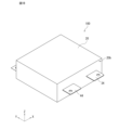
- FIG. 1 A perspective view showing a capacitor module according to Embodiment 1 A view of the capacitor module in Figure 1A from another direction.
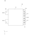
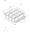
- Top view of the capacitor module in Figure 1 A perspective view of the capacitor module in Figure 1 with the case and sealing resin omitted.
- Exploded perspective view of the capacitor module in Figure 3 A perspective view showing the capacitor element of the capacitor module in FIG. 3
- Top view of the capacitor element in Figure 5A A-A sectional view of the capacitor module in Figure 3
- Capacitor modules are sometimes used, for example, in inverter circuits for vehicles such as hybrid vehicles.
- the drive frequency of the inverter circuit corresponds to a high frequency, so if the ESL (equivalent series inductance) of the capacitor module is large, the surge voltage generated in the inverter circuit becomes large. There is the issue of putting it away. Therefore, it is a challenge to reduce ESL in capacitor modules.
- the capacitor module according to the first aspect of the present invention is a capacitor element having a first end electrode, a second end electrode, and a side surface connecting the first end electrode and the second end electrode; a case accommodating the capacitor element; a first electrode contact portion connected to the first end electrode of the capacitor element and disposed along the first end electrode within the case; and a first electrode contact portion extending from a terminal exposed surface of the case toward the outside of the case.
- a plate-shaped first bus bar having a first terminal portion; a second electrode contact portion connected to the second end electrode of the capacitor element and disposed along the second end electrode within the case; a plate-shaped second bus bar having a second terminal portion that extends and overlaps the first terminal portion in a plan view; a first surface disposed between the first terminal section and the second terminal section, insulating the first terminal section and the second terminal section, and contacting one main surface of the first terminal section; and a second surface that contacts one main surface of the second terminal portion; a sealing resin filled in the case; Equipped with.
- the capacitor element is composed of a laminate of dielectric films,
- the dielectric film may have a glass transition point of 120° C. or higher.
- the heat resistance of the capacitor module can be improved. Therefore, it is possible to provide a capacitor module that can withstand the temperature increase caused by overlapping the first terminal section and the second terminal section.
- the side surface of the capacitor element has a pair of flat parts and a pair of curved parts connecting the pair of flat parts
- the first bus bar may include a first extension part that connects the first electrode contact part and the first terminal part and is arranged along the flat part.
- the side surface of the capacitor element and the first bus bar can be brought close to each other, so that the ESL can be further reduced.
- the second bus bar may include a second extension part that connects the second electrode contact part and the second terminal part and is arranged along the flat part.
- the side surface of the capacitor element and the first bus bar can be brought close to each other, so that the ESL can be further reduced.
- the first bus bar has a third terminal portion extending from the first electrode contact portion and exposed from a surface different from the terminal exposed surface of the case
- the second bus bar has a fourth terminal portion extending from the second electrode contact portion and exposed from a surface different from the terminal exposed surface of the case
- the first terminal portion and the second terminal portion may function as output terminals
- the third terminal portion and the fourth terminal portion may function as input terminals.
- the capacitor module can be provided with a charging terminal.
- the first terminal portion and the second terminal portion may be AC terminals, and the third terminal portion and the fourth terminal portion may be DC terminals.
- the capacitor module can be provided with a charging terminal.
- the third terminal portion and the fourth terminal portion may not overlap in plan view.
- a first through hole penetrating in the thickness direction is formed in the first electrode contact part, and the outer shape of the first through hole is a part of the first electrode contact part toward the inside of the first through hole. constitutes a first mounting portion having a protruding shape, and an end portion of the first mounting portion in a direction approaching the terminal exposed surface is connected to the first electrode contact portion,
- a second through hole penetrating in the thickness direction is formed in the second electrode contact portion, and the outer shape of the second through hole is a portion of the second electrode contact portion toward the inside of the second through hole.
- a first stud for electrically connecting the capacitor element to an external device is arranged in the first terminal portion
- a second stud for electrically connecting the capacitor element to an external device is disposed in the second terminal portion
- the first stud and the second stud may protrude in opposite directions.
- the capacitor module can be easily connected to an external device.
- FIG. 1A is a perspective view showing a capacitor module according to the first embodiment.
- FIG. 1B is a view of the capacitor module of FIG. 1A from another direction.
- FIG. 2 is a top view of the capacitor module of FIG. 1A.
- FIG. 3 is a perspective view of the capacitor module of FIG. 1A with the case and sealing resin omitted.
- FIG. 4 is an exploded perspective view of the capacitor module of FIG. 3. Note that the X, Y, and Z directions in the figure indicate the horizontal direction, vertical direction, and height direction of the capacitor module 100, respectively.
- the capacitor module 100 includes a capacitor element 10, a case 20, a first bus bar 30, a second bus bar 40, an insulator 50, and a sealing resin 60.
- the capacitor element 10 , a portion of the first bus bar 30 , and a portion of the second bus bar 40 are housed in the case 20 and sealed with a sealing resin 60 .
- FIG. 5A is a perspective view showing a capacitor element of the capacitor module of FIG. 3.
- FIG. 5B is a top view of the capacitor element of FIG. 5A.
- the capacitor element 10 will be described with reference to FIGS. 5A and 5B.
- the capacitor element 10 has a first end electrode 11 , a second end electrode 12 , and a side surface 13 that connects the first end electrode 11 and the second end electrode 12 . Further, in this embodiment, the side surface 13 of the capacitor element 10 includes a pair of flat portions 13a facing each other and a pair of curved portions 13b connecting the pair of flat portions 13a.
- the capacitor element 10 is a film capacitor composed of a laminate of dielectric films. More specifically, the capacitor element 10 is formed by stacking dielectric films each having a metal vapor deposited film formed on its surface and then winding the films. In this embodiment, the capacitor element 10 is formed into a columnar shape having an oval cross section by pressing a rolled body of dielectric film into a flat shape.
- the dielectric film for example, a dielectric film formed from a mixed resin solution containing phenoxy resin and MDI (diphenylmethane diisocyanate) can be used.
- a dielectric film formed from a mixed resin solution containing polyvinyl acetoacetal (PVAA) and ethyl acetate may be used.
- PVAA polyvinyl acetoacetal
- ethyl acetate ethyl acetate
- the glass transition point of the dielectric film can be set to 120° C. or higher, and the heat resistance of the capacitor module can be improved.
- metals such as Al and Zn can be used as the metal vapor deposition film formed on the surface of the dielectric film.
- a first end surface electrode 11 is formed at one end of the wound body of dielectric film, and a second end surface electrode 12 is formed at the other end.
- the first end electrode 11 and the second end electrode 12 can be formed, for example, by thermal spraying Zn or the like.
- Case 20 is a case for accommodating capacitor element 10.
- the case 20 has a rectangular parallelepiped shape, as shown in FIGS. 1 and 2, and has an opening that exposes a portion of the first bus bar 30 and the second bus bar 40.
- the case 20 accommodates six capacitor elements 10 shown in FIGS. 3 and 4. Further, a portion of the first bus bar 30 and the second bus bar 40 are also housed within the case 20.
- the case 20 has a first terminal exposed surface 20a and a second terminal exposed surface 20b different from the first terminal exposed surface 20a.
- the first terminal exposed surface 20a exposes a first terminal portion 32 of a first bus bar 30 and a second terminal portion 42 of a second bus bar 40 (see FIGS. 7 and 8), which will be described later.
- the first terminal portion 32 and the second terminal portion 42 are exposed from the first terminal exposed surface 20a of the case 20, and the third terminal portion 34 and the fourth terminal portion 44, which will be described later, are exposed from the second terminal exposed surface 20b. is exposed.
- the case 20 is made of, for example, synthetic resin such as polyphenylene sulfide (PPS resin) and polybutylene terephthalate (PBT resin).
- synthetic resin such as polyphenylene sulfide (PPS resin) and polybutylene terephthalate (PBT resin).
- the first bus bar 30 is a terminal for electrically connecting the first end electrode 11 of the capacitor element 10 and a terminal of an external device (not shown).
- the first bus bar 30 is formed of a conductive member such as a plate-shaped metal.
- the first bus bar 30 has a first electrode contact portion 31 and a first terminal portion 32, as shown in FIGS. 3 and 4.
- the first electrode contact portion 31 is connected to the first end electrode 11 of the capacitor element 10 and is arranged along the first end electrode 11 inside the case 20 .
- the first electrode contact portion 31 is arranged to spread out in the XY plane so as to contact the first end electrodes 11 of all the capacitor elements 10 of the capacitor module 100.
- the first terminal portion 32 extends from the first terminal exposed surface 20a of the case 20 toward the outside of the case 20.
- the first bus bar 30 has a first extending portion 33 that connects the first electrode contact portion 31 and the first terminal portion 32.
- the first bus bar 30 further includes a third terminal portion 34 that extends from the first electrode contact portion 31 and is exposed from the second terminal exposed surface 20b of the case 20.
- the third terminal portion 34 is provided on the opposite side of the first electrode contact portion 31 from the first terminal portion 32 .
- FIG. 6 is a cross-sectional view taken along line AA of the capacitor module in FIG. 3.
- the first electrode contact portion 31 is arranged to contact the first end electrode 11 of each capacitor element 10.
- a first extending portion 33 extends from one end of the first electrode contact portion 31 along the flat portion 13a of the capacitor element 10, and a first terminal portion 32 extends from an end of the first extending portion 33.
- a third terminal portion 34 extends from the other end of the first electrode contact portion 31 .
- the first terminal portion 32 and the third terminal portion 34 of the first bus bar 30 are exposed from the case 20 and arranged.
- the ESL of the capacitor module 100 can be reduced.
- the first terminal portion 32 functions as an output terminal of the capacitor module 100, and an alternating current flows through the first terminal portion 32.
- the third terminal section 34 functions as an input terminal of the capacitor module 100, and a direct current flows through the third terminal section 34.
- the third terminal portion 34 can be used as a charging terminal for the capacitor module 100.
- the first electrode contact portion 31 is formed with a first through hole 35 that penetrates the first bus bar 30 in the thickness direction.
- the outer shape of the first through hole 35 constitutes a first mounting section 36 in which a part of the first electrode contact section 31 protrudes toward the inside of the first through hole 35. is formed integrally with the first electrode contact portion 31.
- first through holes 35 and a first mounting part 36 are formed in the first electrode contact part 31, and in plan view, 12 first through holes 35 and a first mounting part 36 are formed in the first electrode contact part 31.
- Two first mounting sections 36 are arranged. That is, each capacitor element 10 is connected by solder using two first mounting parts 36, respectively.
- the number of first through holes 35 and first mounting portions 36 is not limited to twelve, but may be any number that can electrically connect each capacitor element 10 and first bus bar 30.
- FIG. 7 is a perspective view of the capacitor module of FIG. 3 viewed from another angle.
- FIG. 8 is a BB sectional view of the capacitor module of FIG. 7.
- the second bus bar 40 is a terminal for electrically connecting the second end electrode 12 of the capacitor element 10 and a terminal of an external device (not shown). Note that the basic configuration of the second bus bar 40 is the same as that of the first bus bar 30, so a description thereof will be omitted as appropriate.
- the second bus bar 40 has a second electrode contact part 41 and a second terminal part 42, as shown in FIGS. 4 and 7.
- the second electrode contact portion 41 is connected to the second end electrode 12 of the capacitor element 10 and is arranged along the second end electrode 12 inside the case 20 .
- the second terminal portion 42 extends toward the first terminal exposed surface 20a of the case 20.
- the second bus bar 40 has a second extending portion 43 that connects the second electrode contact portion 41 and the second terminal portion 42.
- the second bus bar 40 further includes a fourth terminal portion 44 that extends from the second electrode contact portion 41 and is exposed from the second terminal exposed surface 20b of the case 20.
- the fourth terminal portion 44 is provided on the opposite side of the second electrode contact portion 41 from the second terminal portion 42 .
- the second electrode contact portion 41 is arranged to contact the second end surface electrode 12 of each capacitor element 10.
- a second extending portion 43 extends from one end of the second electrode contact portion 41 along the flat portion 13a of the capacitor element 10, and a second terminal portion 42 extends from an end of the second extending portion 43.
- the second extending portion 43 is arranged along the flat portion 13 a of the capacitor element 10 in line with the first extending portion 33 of the first bus bar 30 .
- a fourth terminal portion 44 extends from the other end of the second electrode contact portion 41 .
- the second terminal portion 2 and the fourth terminal portion 44 of the second bus bar 40 are exposed from the case 20 and arranged.
- the ESL of the capacitor module 100 can be reduced.
- the second terminal portion 42 functions as an output terminal of the capacitor module 100, and an alternating current flows through the second terminal portion 42.
- the fourth terminal section 44 functions as an input terminal of the capacitor module 100, and a direct current flows through the fourth terminal section 44.
- the fourth terminal portion 44 can be used as a charging terminal for the capacitor module 100.
- the second electrode contact portion 41 is formed with a second through hole 45 that penetrates the second bus bar 40 in the thickness direction.
- the outer shape of the second through hole 45 constitutes a second mounting section 46 in which a part of the second electrode contact section 41 protrudes toward the inside of the second through hole 45. is formed integrally with the second electrode contact portion 41.
- 12 second through holes 45 and second mounting portions 46 are formed in the second electrode contact portion 41, and in plan view, 12 second through holes 45 and a second mounting portion 46 are formed in the second electrode contact portion 41, and in a plan view, Two second mounting sections 46 are arranged. That is, each capacitor element 10 is connected by solder using two second mounting parts 46, respectively.
- the number of second through holes 45 and second mounting portions 46 is not limited to twelve, but may be any number that can electrically connect each capacitor element 10 and second bus bar 40.
- the first terminal portion 32 of the first bus bar 30 and the second terminal portion 42 of the second bus bar 40 are arranged to overlap in the Z direction in a plan view. . Since the insulator 50 is disposed between the first terminal section 32 and the second terminal section 42, the first terminal section 32 and the second terminal section 42 are electrically insulated.
- the third terminal portion 34 and the fourth terminal portion 44 do not overlap in plan view.
- the third terminal section 34 and the fourth terminal section 44 are arranged at shifted positions in the XY direction.
- the insulator 50 is a sheet-like member that is disposed between the first terminal section 32 and the second terminal section 42 and insulates the first terminal section 32 and the second terminal section 42 from each other. By arranging the insulator 50 between the first terminal portion 32 and the second terminal portion 42, short circuit between the terminal portions can be prevented.
- the insulator 50 is made of, for example, insulating paper or insulating resin.
- the insulator 50 has a first surface 50a and a second surface 50b, as shown in FIGS. 6 and 8.
- the first surface 50 a of the insulator 50 contacts one main surface of the first terminal section 32
- the second surface 50 b of the insulator 50 contacts one main surface of the second terminal section 42 .
- the thickness of the insulator 50 is as thin as possible within a range that can sufficiently insulate the first terminal part 32 and the second terminal part 42. .
- the sealing resin 60 is filled in the case 20 to seal the six capacitor elements 10 housed in the case 20 and a portion of the first bus bar 30 and the second bus bar 40.
- the sealing resin 60 is made of, for example, a thermosetting resin such as epoxy resin or urethane resin.
- a thermosetting resin such as epoxy resin or urethane resin.
- the material of the sealing resin 60 it is preferable to use a material with high fluidity and adhesiveness.
- a first stud 70 for connecting the first end electrode 11 of the capacitor element 10 to an external device is arranged at the first terminal portion 32 of the first bus bar 30.
- a second stud 80 for connecting the second end face electrode 12 of the capacitor element 10 to an external device is arranged at the second terminal portion 42 of the second bus bar 40.
- the first stud 70 and the second stud 80 protrude in opposite directions in the Z direction.
- the first stud 70 and the second stud 80 can be configured by, for example, a self-clinching stud that is press-fitted into the terminal portion.
- a self-clinching stud that is press-fitted into the terminal portion.
- the first terminal section 32 and the second terminal section 42 can be arranged parallel to each other, so that the ESL of the capacitor module 100 can be improved. It can be further reduced.
- the first stud 70 and the second stud 80 may be constituted by screws or the like.
- first studs 70 and six second studs 80 are arranged, but the number of studs is not limited to this, and is used to connect external devices. It is sufficient if an appropriate number are placed.
- the capacitor module 100 by arranging the first terminal section 32 and the second terminal section 42 in an overlapping manner in the Z direction, when voltages of different polarities are applied to the first bus bar 30 and the second bus bar 40, Currents flow in opposite directions to the first terminal portion 32 and the second terminal portion 42 .
- the magnetic field due to the current flowing through the first terminal portion 32 and the magnetic field due to the current flowing through the second terminal portion 42 cancel each other out, so that the ESL of the capacitor module 100 can be reduced.
- current concentrates on the first terminal portion 32 and the second terminal portion 42 because they are current entry and exit ports. Therefore, the effect of reducing ESL by overlapping the first terminal portion 32 and the second terminal portion 42 is large.
- the heat conductivity of the capacitor module 100 increases, and the first terminal section 32 and the second terminal section 42 tend to generate heat when current flows. . Furthermore, since both the first extending portion 33 and the second extending portion 43 are arranged along the side surface of the capacitor element 10, the center temperature of the capacitor element 10 tends to rise. In this embodiment, since a film having a glass transition point of 120° C. or higher is used as the dielectric film constituting the capacitor element 10, the heat resistance can be higher than that of conventional capacitor elements. Therefore, the capacitor module 100 has heat resistance against increases in the center temperature of the capacitor element 10.
- the first extending portion 33 and the second extending portion 43 have different lengths in the Z direction. Specifically, the first extending portion 33 is formed longer than the second extending portion 43. Since the lengths of the first stretched portion 33 and the second stretched portion 43 do not easily affect the ESL reduction of the capacitor module 100, for example, even if the second stretched portion 43 is longer than the first stretched portion 33, Alternatively, the first extending portion 33 and the second extending portion 43 may have the same length. Alternatively, the extending portion may be formed only on either one of the first bus bar 30 and the second bus bar 40.
- the end of the first mounting portion 36 in the direction approaching the first terminal exposed surface 20a of the case 20 is connected to the first electrode contact portion 31.
- the first mounting portion 36 is connected to the first electrode contact portion 31 in a direction approaching the first terminal exposed surface 20a, thereby shortening the distance through which current flows between the capacitor element 10 and the first terminal portion 32. This contributes to reducing the ESL of the capacitor module 100.
- the end of the second mounting portion 46 in the direction approaching the first terminal exposed surface 20a of the case 20 is connected to the second electrode contact portion 41.
- the second mounting portion 46 is connected to the second electrode contact portion 41 in a direction approaching the first terminal exposed surface 20a, thereby shortening the distance through which current flows between the capacitor element 10 and the second terminal portion 42. This contributes to reducing the ESL of the capacitor module 100.
- the third terminal portion 34 and the fourth terminal portion 44 are arranged without overlapping.
- the third terminal section 34 and the fourth terminal section 44 are terminals used for charging the capacitor module 100, and direct current flows therethrough. Therefore, even when the third terminal section 34 and the fourth terminal section 44 do not overlap, the ESL reduction of the capacitor module 100 is less affected.
- the capacitor module 100 includes a capacitor element 10, a case 20, a first bus bar 30, a second bus bar 40, an insulator 50, and a sealing resin 60.
- the capacitor element 10 has a first end electrode 11 , a second end electrode 12 , and a side surface 13 connecting the first end electrode 11 and the second end electrode 12 .
- Case 20 houses capacitor element 10 .
- the first bus bar 30 is connected to the first end electrode 11 of the capacitor element 10 and includes a first electrode contact portion 31 disposed along the first end electrode 11 inside the case 20 and a first terminal exposed surface of the case 20. It has a first terminal portion 32 extending toward 20a.
- the second bus bar 40 includes a second electrode contact portion 41 connected to the second end electrode 12 of the capacitor element 10 and arranged along the second end electrode 12 inside the case 20, and a first terminal exposed surface of the case 20. It has a second terminal part 42 that extends toward 20a and overlaps the first terminal part 32 in plan view.
- the insulator 50 is disposed between the first terminal portion 32 and the second terminal portion 42 to insulate the first terminal portion 32 and the second terminal portion 42, and is provided on one main surface of the first terminal portion 32. It has a first surface 50a that contacts, and a second surface 50b that contacts one main surface of the second terminal portion 42.
- the case 20 is filled with the sealing resin 60 .
- the ESL of the capacitor module 100 can be reduced.
- the capacitor element 10 is composed of a laminate of dielectric films, and the glass transition point of the dielectric film is 120° C. or higher.
- a capacitor module with high heat resistance can be provided.
- the first terminal section 32 and the second terminal section 42 are arranged in an overlapping manner, heat transferability is increased and heat is easily transmitted between the terminals, leading to an increase in the temperature of the capacitor module 100.
- the capacitor element 10 made of a laminate of highly heat-resistant dielectric films with a glass transition point of 120° C. or higher it is possible to provide a capacitor module with improved heat resistance while reducing ESL.
- the side surface 13 of the capacitor element 10 has a pair of flat parts 13a and a pair of curved parts 13b connecting the pair of flat parts 13a.
- the first bus bar 30 connects the first electrode contact portion 31 and the first terminal portion 32 and has a first extending portion 33 arranged along the flat portion 13a.
- the side surface 13 of the capacitor element 10 and the first bus bar 30 can be brought close to each other, so that the ESL of the capacitor module 100 can be further reduced.
- the second bus bar 40 connects the second electrode contact portion 41 and the second terminal portion 42 and has a second extension portion 43 arranged along the flat portion 13a.
- the side surface 13 of the capacitor element 10 and the first bus bar 30 can be brought close to each other, so that the ESL of the capacitor module 100 can be further reduced.
- the first bus bar 30 has a third terminal portion 34 that extends from the first electrode contact portion 31 and is exposed from a surface different from the first terminal exposed surface 20a of the case 20.
- the second bus bar 40 has a fourth terminal portion 44 that extends from the second electrode contact portion 41 and is exposed from a surface different from the first terminal exposed surface 20a of the case 20.
- the first terminal section 32 and the second terminal section 42 function as output terminals, and the third terminal section 34 and the fourth terminal section 44 function as input terminals.
- the capacitor module 100 can be provided with a charging terminal.
- the first terminal part 32 and the second terminal part 42 are AC terminals, and the third terminal part 34 and the fourth terminal part 44 are DC terminals.
- the capacitor module 100 can be provided with a charging terminal.
- the third terminal portion 34 and the fourth terminal portion 44 do not overlap in plan view.
- the degree of freedom in designing the capacitor module 100 can be improved.
- a first through hole 35 penetrating in the thickness direction is formed in the first electrode contact portion 31 , and the outer shape of the first through hole 35 is the same as that of the first electrode contact portion 31 toward the inside of the first through hole 35 .
- the first mounting portion 36 has a protruding portion. The first mounting portion 36 is connected to the first electrode contact portion 31 at its end in the direction approaching the first terminal exposed surface 20a.
- a second through hole 45 penetrating in the thickness direction is formed in the second electrode contact portion 41 , and the outer shape of the second through hole 45 is the same as that of the second electrode contact portion 41 toward the inside of the second through hole 45 .
- the second mounting portion 46 has a protruding portion. The end of the second mounting portion 46 in the direction approaching the first terminal exposed surface 20a is connected to the second electrode contact portion 41.
- the distance through which current flows from the first end surface electrode 11 to the first terminal section 32 and from the second end surface electrode 12 to the second terminal section 42 can be shortened. Therefore, the ESL of the capacitor module 100 can be further reduced.
- a first stud 70 for electrically connecting the capacitor element 10 to an external device is arranged in the first terminal part 32, and a first stud 70 for electrically connecting the capacitor element 10 to an external device is arranged in the second terminal part 42.
- a second stud 80 is arranged for this purpose.
- the capacitor module 100 can be easily connected to an external device.
- the first bus bar 30 has the first extending part 33 and the third terminal part 34
- the second bus bar 40 has the second extending part 43 and the fourth terminal part 44.
- the first bus bar 30 and the second bus bar 40 do not need to have an extending portion.
- the first bus bar 30 and the second bus bar 40 do not need to have the third terminal section 34 and the fourth terminal section 44.
- the capacitor element 10 is formed in a columnar shape having an elliptical cross section, but the present invention is not limited thereto.
- the capacitor element 10 may be formed in, for example, a cylindrical shape or a polygonal prism shape such as a quadrangular prism.
- the insulator 50 is disposed between the first terminal section 32 and the second terminal section 42, but the present invention is not limited to this.
- the insulator 50 at least one of one main surface of the first terminal section 32 and one main surface of the second terminal section 42 may be coated with an insulating coating.
- the capacitor module of the present invention includes a capacitor element having a first end electrode, a second end electrode, a side surface connecting the first end electrode and the second end electrode, and a case housing the capacitor element. a first electrode contact portion connected to the first end electrode of the capacitor element and disposed along the first end electrode within the case; and a first terminal portion extending from the terminal exposed surface of the case toward the outside of the case. and a second electrode contact portion connected to the second end electrode of the capacitor element and disposed along the second end electrode within the case; A plate-shaped second bus bar having a second terminal portion that extends toward the outside of the case and overlaps the first terminal portion in a plan view, and is disposed between the first terminal portion and the second terminal portion.
- first surface that insulates the first terminal portion and the second terminal portion, and that contacts one main surface of the first terminal portion, and a second surface that contacts one main surface of the second terminal portion. It includes an insulator and a sealing resin filled in the case.
- the capacitor element is constituted by a laminate of dielectric films, and the dielectric film may have a glass transition point of 120° C. or higher.
- the side surface of the capacitor element has a pair of flat parts and a pair of curved parts connecting the pair of flat parts
- the first bus bar has a first
- the electrode contact portion and the first terminal portion may be connected to each other, and a first extending portion may be provided along the flat portion.
- the second bus bar connects the second electrode contact part and the second terminal part, and the second extending part is arranged along the flat part. , may have.
- the first bus bar has a third terminal portion that extends from the first electrode contact portion and is exposed from a surface different from the terminal exposed surface of the case.
- the second bus bar has a fourth terminal portion that extends from the second electrode contact portion and is exposed from a surface different from the terminal exposed surface of the case, and the first terminal portion and the second terminal portion function as output terminals.
- the third terminal section and the fourth terminal section may function as input terminals.
- the first terminal portion and the second terminal portion may be AC terminals, and the third terminal portion and the fourth terminal portion may be DC terminals.
- the third terminal portion and the fourth terminal portion do not need to overlap in plan view.
- a first through hole penetrating in the thickness direction is formed in the first electrode contact portion, and the outer shape of the first through hole is the same as the first through hole.
- the first mounting part has a shape in which a part of the first electrode contact part protrudes toward the inside of the through hole, and the end of the first mounting part in the direction approaching the terminal exposed surface is the first electrode contact part.
- a second through hole penetrating in the thickness direction is formed in the second electrode contact portion, and the outer shape of the second through hole is a part of the second electrode contact portion toward the inside of the second through hole. constitutes a second mounting portion having a protruding shape, and the end portion of the second mounting portion in the direction approaching the terminal exposed surface may be connected to the second electrode contact portion.
- a first stud for electrically connecting the capacitor element to an external device is disposed in the first terminal part, and a first stud for electrically connecting the capacitor element to an external device is disposed in the first terminal part.
- a second stud for electrically connecting the capacitor element to an external device is disposed on the capacitor element, and the first stud and the second stud may protrude in opposite directions.
- the present invention is useful for film capacitors used in various electronic devices, electrical devices, industrial devices, vehicle devices, etc.
Landscapes
- Engineering & Computer Science (AREA)
- Power Engineering (AREA)
- Microelectronics & Electronic Packaging (AREA)
- Manufacturing & Machinery (AREA)
- Fixed Capacitors And Capacitor Manufacturing Machines (AREA)
Abstract
コンデンサモジュールは、第1端面電極と、第2端面電極と、第1端面電極と第2端面電極と、を接続する側面とを有するコンデンサ素子と、コンデンサ素子を収容するケースと、コンデンサ素子の前記第1端面電極に接続され、ケース内で第1端面電極に沿って配置される第1電極接触部と、ケースの端子露出面からケースの外側に向かって延びる第1端子部と、を有する板状の第1バスバーと、コンデンサ素子の第2端面電極に接続され、ケース内で第2端面電極に沿って配置される第2電極接触部と、ケースの端子露出面からケースの外側に向かって延びて、平面視で第1端子部と重なる第2端子部と、を有する板状の第2バスバーと、第1端子部と第2端子部との間に配置されて、第1端子部と第2端子部とを絶縁し、第1端子部の一方主面に接触する第1面と、第2端子部の一方主面に接触する第2面と、を有する絶縁体と、ケースに充填される封止樹脂と、を備える。
Description
本発明は、コンデンサモジュールに関する。
コンデンサ素子の第1電極に第1バスバーを接続し、第2電極も第2バスバーを接続したコンデンサモジュールが知られている。
例えば、特許文献1には、一対の電極を有するコンデンサ素子の一対の電極の一方と電気的に接続された第1バスバーと、一対の電極の他方と電気的に接続された第2バスバーと、を備えるコンデンサモジュールが記載されている。
特許文献1に記載のコンデンサモジュールは、ESLを低減させる点で未だ改善の余地がある。
本発明は、ESLを低減することのできるコンデンサモジュールを提供する。
本発明の一態様にかかるコンデンサモジュールは、
第1端面電極と、第2端面電極と、第1端面電極と第2端面電極と、を接続する側面とを有するコンデンサ素子と、
前記コンデンサ素子を収容するケースと、
前記コンデンサ素子の前記第1端面電極に接続され、前記ケース内で前記第1端面電極に沿って配置される第1電極接触部と、前記ケースの端子露出面から前記ケースの外側に向かって延びる第1端子部と、を有する板状の第1バスバーと、
前記コンデンサ素子の前記第2端面電極に接続され、前記ケース内で前記第2端面電極に沿って配置される第2電極接触部と、前記ケースの前記端子露出面から前記ケースの外側に向かって延びて、平面視で前記第1端子部と重なる第2端子部と、を有する板状の第2バスバーと、
前記第1端子部と前記第2端子部との間に配置されて、前記第1端子部と前記第2端子部とを絶縁し、前記第1端子部の一方主面に接触する第1面と、前記第2端子部の一方主面に接触する第2面と、を有する絶縁体と、
前記ケースに充填される封止樹脂と、
を備える。
第1端面電極と、第2端面電極と、第1端面電極と第2端面電極と、を接続する側面とを有するコンデンサ素子と、
前記コンデンサ素子を収容するケースと、
前記コンデンサ素子の前記第1端面電極に接続され、前記ケース内で前記第1端面電極に沿って配置される第1電極接触部と、前記ケースの端子露出面から前記ケースの外側に向かって延びる第1端子部と、を有する板状の第1バスバーと、
前記コンデンサ素子の前記第2端面電極に接続され、前記ケース内で前記第2端面電極に沿って配置される第2電極接触部と、前記ケースの前記端子露出面から前記ケースの外側に向かって延びて、平面視で前記第1端子部と重なる第2端子部と、を有する板状の第2バスバーと、
前記第1端子部と前記第2端子部との間に配置されて、前記第1端子部と前記第2端子部とを絶縁し、前記第1端子部の一方主面に接触する第1面と、前記第2端子部の一方主面に接触する第2面と、を有する絶縁体と、
前記ケースに充填される封止樹脂と、
を備える。
本発明によると、ESLを低減することのできるコンデンサモジュールを提供することができる。
(本発明に至った経緯)
コンデンサモジュールは、例えばハイブリッド自動車などの車載用のインバータ回路に使用されることがある。コンデンサモジュールがインバータ回路で使用される場合、インバータ回路の駆動周波数が高周波に対応した周波数であるため、コンデンサモジュールのESL(等価直列インダクタンス)が大きいと、インバータ回路において発生するサージ電圧が大きくなってしまうという課題がある。したがって、コンデンサモジュールにおいて、ESLを低減することが課題となっている。
コンデンサモジュールは、例えばハイブリッド自動車などの車載用のインバータ回路に使用されることがある。コンデンサモジュールがインバータ回路で使用される場合、インバータ回路の駆動周波数が高周波に対応した周波数であるため、コンデンサモジュールのESL(等価直列インダクタンス)が大きいと、インバータ回路において発生するサージ電圧が大きくなってしまうという課題がある。したがって、コンデンサモジュールにおいて、ESLを低減することが課題となっている。
しかし、特許文献1に記載のコンデンサモジュールでは、十分にESLを低減させることが難しい。そこで、本発明者らは、さらにESLを低減させることのできるコンデンサモジュールについて検討し、以下の発明に至った。
本発明の第1態様にかかるコンデンサモジュールは、
第1端面電極と、第2端面電極と、第1端面電極と第2端面電極と、を接続する側面とを有するコンデンサ素子と、
前記コンデンサ素子を収容するケースと、
前記コンデンサ素子の前記第1端面電極に接続され、前記ケース内で前記第1端面電極に沿って配置される第1電極接触部と、前記ケースの端子露出面から前記ケースの外側に向かって延びる第1端子部と、を有する板状の第1バスバーと、
前記コンデンサ素子の前記第2端面電極に接続され、前記ケース内で前記第2端面電極に沿って配置される第2電極接触部と、前記ケースの前記端子露出面から前記ケースの外側に向かって延びて、平面視で前記第1端子部と重なる第2端子部と、を有する板状の第2バスバーと、
前記第1端子部と前記第2端子部との間に配置されて、前記第1端子部と前記第2端子部とを絶縁し、前記第1端子部の一方主面に接触する第1面と、前記第2端子部の一方主面に接触する第2面と、を有する絶縁体と、
前記ケースに充填される封止樹脂と、
を備える。
第1端面電極と、第2端面電極と、第1端面電極と第2端面電極と、を接続する側面とを有するコンデンサ素子と、
前記コンデンサ素子を収容するケースと、
前記コンデンサ素子の前記第1端面電極に接続され、前記ケース内で前記第1端面電極に沿って配置される第1電極接触部と、前記ケースの端子露出面から前記ケースの外側に向かって延びる第1端子部と、を有する板状の第1バスバーと、
前記コンデンサ素子の前記第2端面電極に接続され、前記ケース内で前記第2端面電極に沿って配置される第2電極接触部と、前記ケースの前記端子露出面から前記ケースの外側に向かって延びて、平面視で前記第1端子部と重なる第2端子部と、を有する板状の第2バスバーと、
前記第1端子部と前記第2端子部との間に配置されて、前記第1端子部と前記第2端子部とを絶縁し、前記第1端子部の一方主面に接触する第1面と、前記第2端子部の一方主面に接触する第2面と、を有する絶縁体と、
前記ケースに充填される封止樹脂と、
を備える。
このような構成により、ESLを低減させることのできるコンデンサモジュールを提供することができる。
本発明の第2態様にかかるコンデンサモジュールにおいて、
前記コンデンサ素子は、誘電体フィルムの積層体により構成され、
前記誘電体フィルムのガラス転移点は、120℃以上であってもよい。
前記コンデンサ素子は、誘電体フィルムの積層体により構成され、
前記誘電体フィルムのガラス転移点は、120℃以上であってもよい。
このような構成により、コンデンサモジュールの耐熱性を向上させることができる。このため、第1端子部と第2端子部とを重ねたことによる温度上昇に耐えうるコンデンサモジュールを提供することができる。
本発明の第3態様にかかるコンデンサモジュールにおいて、
前記コンデンサ素子の前記側面は、一対の平坦部と、前記一対の平坦部を繋ぐ一対の湾曲部と、を有し、
前記第1バスバーは、前記第1電極接触部と前記第1端子部とを繋ぎ、前記平坦部に沿って配置される第1延伸部、を有してもよい。
前記コンデンサ素子の前記側面は、一対の平坦部と、前記一対の平坦部を繋ぐ一対の湾曲部と、を有し、
前記第1バスバーは、前記第1電極接触部と前記第1端子部とを繋ぎ、前記平坦部に沿って配置される第1延伸部、を有してもよい。
このような構成により、コンデンサ素子の側面と第1バスバーとを近接させることができるため、さらにESLを低減させることができる。
本発明の第4態様にかかるコンデンサモジュールにおいて、
前記第2バスバーは、前記第2電極接触部と前記第2端子部とを繋ぎ、前記平坦部に沿って配置される第2延伸部、を有してもよい。
前記第2バスバーは、前記第2電極接触部と前記第2端子部とを繋ぎ、前記平坦部に沿って配置される第2延伸部、を有してもよい。
このような構成により、コンデンサ素子の側面と第1バスバーとを近接させることができるため、さらにESLを低減させることができる。
本発明の第5態様にかかるコンデンサモジュールにおいて、
前記第1バスバーは、前記第1電極接触部から延びて、前記ケースの前記端子露出面と異なる面から露出する第3端子部を有し、
前記第2バスバーは、前記第2電極接触部から延びて、前記ケースの前記端子露出面と異なる面から露出する第4端子部を有し、
前記第1端子部と前記第2端子部とは出力端子として機能し、前記第3端子部と前記第4端子部とは入力端子として機能してもよい。
前記第1バスバーは、前記第1電極接触部から延びて、前記ケースの前記端子露出面と異なる面から露出する第3端子部を有し、
前記第2バスバーは、前記第2電極接触部から延びて、前記ケースの前記端子露出面と異なる面から露出する第4端子部を有し、
前記第1端子部と前記第2端子部とは出力端子として機能し、前記第3端子部と前記第4端子部とは入力端子として機能してもよい。
このような構成により、コンデンサモジュールに充電用の端子を設けることができる。
本発明の第6態様にかかるコンデンサモジュールにおいて、
前記第1端子部および前記第2端子部は、交流端子であり、前記第3端子部および前記第4端子部は、直流端子であってもよい。
前記第1端子部および前記第2端子部は、交流端子であり、前記第3端子部および前記第4端子部は、直流端子であってもよい。
このような構成により、コンデンサモジュールに充電用の端子を設けることができる。
本発明の第7態様にかかるコンデンサモジュールにおいて、
前記第3端子部と前記第4端子部とは、平面視において重なっていなくてもよい。
前記第3端子部と前記第4端子部とは、平面視において重なっていなくてもよい。
このような構成により、コンデンサモジュールの設計自由度を向上させることができる。
本発明の第8態様にかかるコンデンサモジュールにおいて、
前記第1電極接触部には、厚み方向に貫通する第1貫通孔が形成され、前記第1貫通孔の外形は、前記第1貫通孔の内側に向かって前記第1電極接触部の一部が突出した形状の第1実装部を構成し、前記第1実装部は、前記端子露出面に近付く方向の端部が前記第1電極接触部と繋がっており、
前記第2電極接触部には、厚み方向に貫通する第2貫通孔が形成され、前記第2貫通孔の外形は、前記第2貫通孔の内側に向かって前記第2電極接触部の一部が突出した形状の第2実装部を構成し、前記第2実装部は、前記端子露出面に近付く方向の端部が前記第2電極接触部と繋がっていてもよい。
前記第1電極接触部には、厚み方向に貫通する第1貫通孔が形成され、前記第1貫通孔の外形は、前記第1貫通孔の内側に向かって前記第1電極接触部の一部が突出した形状の第1実装部を構成し、前記第1実装部は、前記端子露出面に近付く方向の端部が前記第1電極接触部と繋がっており、
前記第2電極接触部には、厚み方向に貫通する第2貫通孔が形成され、前記第2貫通孔の外形は、前記第2貫通孔の内側に向かって前記第2電極接触部の一部が突出した形状の第2実装部を構成し、前記第2実装部は、前記端子露出面に近付く方向の端部が前記第2電極接触部と繋がっていてもよい。
このような構成により、コンデンサ素子の端面電極とバスバーの第1端子部または第2端子部との間の電流の流れる距離を短くすることができるため、さらにESLを低減させることができる。
本発明の第9態様にかかるコンデンサモジュールにおいて、
前記第1端子部には、前記コンデンサ素子を外部装置に電気的に接続するための第1スタッドが配置され、
前記第2端子部には、前記コンデンサ素子を外部装置に電気的に接続するための第2スタッドが配置され、
前記第1スタッドと前記第2スタッドとは、逆向きに突出していてもよい。
前記第1端子部には、前記コンデンサ素子を外部装置に電気的に接続するための第1スタッドが配置され、
前記第2端子部には、前記コンデンサ素子を外部装置に電気的に接続するための第2スタッドが配置され、
前記第1スタッドと前記第2スタッドとは、逆向きに突出していてもよい。
このような構成により、コンデンサモジュールを容易に外部装置に接続することができる。
以下、本発明にかかる実施の形態1について、添付の図面を参照しながら説明する。また、各図においては、説明を容易なものとするため、各要素を概略的に示している。
(実施の形態1)
[全体構成]
図1Aは、実施の形態1にかかるコンデンサモジュールを示す斜視図である。図1Bは、図1Aのコンデンサモジュールを別の方向から見た図である。図2は、図1Aのコンデンサモジュールの平面図である。図3は、図1Aのコンデンサモジュールのケースおよび封止樹脂を省略した斜視図である。図4は、図3のコンデンサモジュールの分解斜視図である。なお、図中のX、Y、Z方向はそれぞれ、コンデンサモジュール100の横方向、縦方向、高さ方向を示す。
[全体構成]
図1Aは、実施の形態1にかかるコンデンサモジュールを示す斜視図である。図1Bは、図1Aのコンデンサモジュールを別の方向から見た図である。図2は、図1Aのコンデンサモジュールの平面図である。図3は、図1Aのコンデンサモジュールのケースおよび封止樹脂を省略した斜視図である。図4は、図3のコンデンサモジュールの分解斜視図である。なお、図中のX、Y、Z方向はそれぞれ、コンデンサモジュール100の横方向、縦方向、高さ方向を示す。
図1A~図4に示すように、コンデンサモジュール100は、コンデンサ素子10と、ケース20と、第1バスバー30と、第2バスバー40と、絶縁体50と、封止樹脂60と、を備える。本実施の形態では、ケース20に、コンデンサ素子10と、第1バスバー30の一部と、第2バスバー40の一部と、が収容されて、封止樹脂60で封止されている。
以下、コンデンサモジュール100のそれぞれの構成要素について説明する。
<コンデンサ素子>
図5Aは、図3のコンデンサモジュールのコンデンサ素子を示す斜視図である。図5Bは、図5Aのコンデンサ素子の平面図である。図5Aおよび図5Bを参照して、コンデンサ素子10について説明する。
図5Aは、図3のコンデンサモジュールのコンデンサ素子を示す斜視図である。図5Bは、図5Aのコンデンサ素子の平面図である。図5Aおよび図5Bを参照して、コンデンサ素子10について説明する。
コンデンサ素子10は、第1端面電極11と、第2端面電極12と、第1端面電極11と第2端面電極12と接続する側面13と、を有する。また、本実施の形態では、コンデンサ素子10の側面13は、向かい合う一対の平坦部13aと、一対の平坦部13aを繋ぐ一対の湾曲部13bと、を有する。
コンデンサ素子10は、誘電体フィルムの積層体により構成されるフィルムコンデンサである。より具体的には、コンデンサ素子10は、表面に金属蒸着膜を形成した誘電体フィルムを積み重ねた後、巻回することにより形成される。本実施の形態では、誘電体フィルムの巻回体を扁平形状にプレスすることにより、コンデンサ素子10が長円形状の断面を有する柱状に形成されている。
誘電体フィルムとしては、例えば、フェノキシ樹脂とMDI(ジフェニルメタンジイソシアネート)とを含む混合樹脂溶液により形成される誘電体フィルムを使用することができる。または、ポリビニルアセトアセタール(PVAA)と酢酸エチルとを含む混合樹脂溶液により形成される誘電体フィルムを使用してもよい。このような混合樹脂溶液により、誘電体フィルムを形成することで、誘電体フィルムのガラス転移点を120℃以上とすることができ、コンデンサモジュールの耐熱性の向上を実現することができる。誘電体フィルムの表面に形成される金属蒸着膜として、例えば、Al、Zn等の金属を使用することができる。
誘電体フィルムの巻回体の一方の端部に第1端面電極11が形成され、他方の端部に第2端面電極12が形成される。第1端面電極11および第2端面電極12は、例えば、Zn等を溶射することにより形成することができる。
<ケース>
ケース20は、コンデンサ素子10を収容するためのケースである。本実施の形態では、ケース20は、図1および図2に示すように、直方体状の形状を有し、第1バスバー30および第2バスバー40の一部を露出する開口部を有する。ケース20には、図3および図4に示す6つのコンデンサ素子10が収容されている。また、第1バスバー30および第2バスバー40の一部も、ケース20内に収容されている。
ケース20は、コンデンサ素子10を収容するためのケースである。本実施の形態では、ケース20は、図1および図2に示すように、直方体状の形状を有し、第1バスバー30および第2バスバー40の一部を露出する開口部を有する。ケース20には、図3および図4に示す6つのコンデンサ素子10が収容されている。また、第1バスバー30および第2バスバー40の一部も、ケース20内に収容されている。
ケース20は、図2に示すように、第1端子露出面20aと、第1端子露出面20aと異なる第2端子露出面20bと、を有する。第1端子露出面20aは、後述する第1バスバー30の第1端子部32と第2バスバー40の第2端子部42(図7および図8参照)とを露出させる。言い換えると、ケース20の第1端子露出面20aから第1端子部32と第2端子部42とが露出し、第2端子露出面20bから後述する第3端子部34と第4端子部44とが露出している。
ケース20は、例えば、ポリフェニレンサルファイド(PPS樹脂)、ポリブチレンテレフタレート(PBT樹脂)等の合成樹脂等により形成される。
<第1バスバー>
第1バスバー30は、コンデンサ素子10の第1端面電極11と、図示省略の外部装置の端子とを電気的に接続するための端子である。
第1バスバー30は、コンデンサ素子10の第1端面電極11と、図示省略の外部装置の端子とを電気的に接続するための端子である。
第1バスバー30は、例えば板状の金属などの導電性部材により形成される。第1バスバー30は、図3および図4に示すように、第1電極接触部31と、第1端子部32と、を有する。第1電極接触部31は、コンデンサ素子10の第1端面電極11に接続され、ケース20の内部で第1端面電極11に沿って配置される。第1電極接触部31は、コンデンサモジュール100のすべてのコンデンサ素子10の第1端面電極11に接触するよう、XY平面に広がって配置されている。第1端子部32は、ケース20の第1端子露出面20aからケース20の外側に向かって延びる。また、本実施の形態では、第1バスバー30は、第1電極接触部31と第1端子部32とを繋ぐ第1延伸部33を有する。本実施の形態では、さらに、第1バスバー30は、第1電極接触部31から延びて、ケース20の第2端子露出面20bから露出する第3端子部34を有する。本実施の形態では、第3端子部34は第1電極接触部31の第1端子部32と反対側に設けられている。
図6は、図3のコンデンサモジュールのA-A断面図である。図3および図6に示すように、第1電極接触部31は、それぞれのコンデンサ素子10の第1端面電極11に接触するように配置されている。第1電極接触部31の一方の端部から、コンデンサ素子10の平坦部13aに沿って第1延伸部33が延び、第1延伸部33の端部から第1端子部32が延びている。また、第1電極接触部31の他方の端部から、第3端子部34が延びている。第1バスバー30のうち、第1端子部32と第3端子部34とは、ケース20から露出して配置される。
第1延伸部33がコンデンサ素子10の平坦部13aに沿って近接して配置されることで、コンデンサモジュール100のESLを低減することができる。
第1端子部32は、コンデンサモジュール100の出力端子として機能し、第1端子部32には交流電流が流れる。一方、第3端子部34は、コンデンサモジュール100の入力端子として機能し、第3端子部34には直流電流が流れる。第3端子部34は、コンデンサモジュール100の充電用の端子として使用することができる。
図3に示すように、第1電極接触部31には、第1バスバー30の厚み方向に貫通する第1貫通孔35が形成されている。第1貫通孔35の外形は、第1貫通孔35の内側に向かって、第1電極接触部31の一部が突出した形状の第1実装部36を構成しており、第1実装部36は、第1電極接触部31と一体的に形成されている。第1実装部36とコンデンサ素子10の第1端面電極11とを半田で接続することにより、第1バスバー30とコンデンサ素子10の第1端面電極11とが電気的に接続される。
本実施の形態では、第1電極接触部31に12個の第1貫通孔35および第1実装部36が形成されており、平面視において、1つのコンデンサ素子10の第1端面電極11に対して2つの第1実装部36が配置される。すなわち、それぞれのコンデンサ素子10は、それぞれ2つの第1実装部36を用いて半田により接続される。第1貫通孔35および第1実装部36の数は12個に限定されず、それぞれのコンデンサ素子10と第1バスバー30とを電気的に接続することのできる数であればよい。
<第2バスバー>
図7は、図3のコンデンサモジュールを別の角度から見た斜視図である。図8は、図7のコンデンサモジュールのB-B断面図である。
図7は、図3のコンデンサモジュールを別の角度から見た斜視図である。図8は、図7のコンデンサモジュールのB-B断面図である。
第2バスバー40は、コンデンサ素子10の第2端面電極12と、図示省略の外部装置の端子とを電気的に接続するための端子である。なお、第2バスバー40の基本的な構成は、第1バスバー30と同じであるため、適宜説明を省略する。
第2バスバー40は、図4および図7に示すように、第2電極接触部41と、第2端子部42と、を有する。第2電極接触部41は、コンデンサ素子10の第2端面電極12に接続され、ケース20の内部で第2端面電極12に沿って配置される。第2端子部42は、ケース20の第1端子露出面20aに向かって延びる。また、本実施の形態では、第2バスバー40は、第2電極接触部41と第2端子部42とを繋ぐ第2延伸部43を有する。本実施の形態では、さらに、第2バスバー40は、第2電極接触部41から延びて、ケース20の第2端子露出面20bから露出する第4端子部44を有する。本実施の形態では、第4端子部44は第2電極接触部41の第2端子部42と反対側に設けられている。
図8に示すように、第2電極接触部41は、それぞれのコンデンサ素子10の第2端面電極12に接触するように配置されている。第2電極接触部41の一方の端部から、コンデンサ素子10の平坦部13aに沿って第2延伸部43が伸び、第2延伸部43の端部から第2端子部42が延びている。第2延伸部43は、第1バスバー30の第1延伸部33と並んで、コンデンサ素子10の平坦部13aに沿って配置されている。また、第2電極接触部41の他方の端部から、第4端子部44が延びている。第2バスバー40のうち、第2端子部と2と第4端子部44とは、ケース20から露出して配置される。
第2延伸部43がコンデンサ素子10の平坦部13aに沿って配置されることで、コンデンサモジュール100のESLを低減することができる。
第2端子部42は、コンデンサモジュール100の出力端子として機能し、第2端子部42には交流電流が流れる。一方、第4端子部44は、コンデンサモジュール100の入力端子として機能し、第4端子部44には直流電流が流れる。第4端子部44は、コンデンサモジュール100の充電用の端子として使用することができる。
図7に示すように、第2電極接触部41には、第2バスバー40の厚み方向に貫通する第2貫通孔45が形成されている。第2貫通孔45の外形は、第2貫通孔45の内側に向かって、第2電極接触部41の一部が突出した形状の第2実装部46を構成しており、第2実装部46は、第2電極接触部41と一体的に形成されている。第2実装部46とコンデンサ素子10の第2端面電極12とを半田で接続することにより、第2バスバー40とコンデンサ素子10の第2端面電極12とが電気的に接続される。
本実施の形態では、第2電極接触部41に12個の第2貫通孔45および第2実装部46が形成されており、平面視において、1つのコンデンサ素子10の第2端面電極12に対して2つの第2実装部46が配置される。すなわち、それぞれのコンデンサ素子10は、それぞれ2つの第2実装部46を用いて半田により接続される。第2貫通孔45および第2実装部46の数は12個に限定されず、それぞれのコンデンサ素子10と第2バスバー40とを電気的に接続することのできる数であればよい。
図3、および図6~図8に示すように、第1バスバー30の第1端子部32と第2バスバー40の第2端子部42とは、平面視においてZ方向に重なって配置されている。第1端子部32と第2端子部42との間には、絶縁体50が配置されているため、第1端子部32と第2端子部42とは、電気的に絶縁されている。
本実施の形態では、図2に示すように、平面視において第3端子部34と第4端子部44とは重なっていない。言い換えると、第3端子部34と第4端子部44とは、XY方向において、ずれた位置に配置されている。
<絶縁体>
絶縁体50は、第1端子部32と第2端子部42との間に配置されて、第1端子部32と第2端子部42とを絶縁するシート状の部材である。絶縁体50を第1端子部32と第2端子部42との間に配置することで、端子部同士の短絡を防止することができる。絶縁体50は、例えば、絶縁紙または絶縁性樹脂などにより形成される。絶縁体50は、図6および図8に示すように、第1面50aと、第2面50bとを有する。絶縁体50の第1面50aは、第1端子部32の一方主面に接触し、絶縁体50の第2面50bは、第2端子部42の一方主面に接触する。第1端子部32と第2端子部42との距離を小さくするため、絶縁体50の厚さは第1端子部32と第2端子部42とを十分に絶縁できる範囲でできるだけ薄い方が好ましい。
絶縁体50は、第1端子部32と第2端子部42との間に配置されて、第1端子部32と第2端子部42とを絶縁するシート状の部材である。絶縁体50を第1端子部32と第2端子部42との間に配置することで、端子部同士の短絡を防止することができる。絶縁体50は、例えば、絶縁紙または絶縁性樹脂などにより形成される。絶縁体50は、図6および図8に示すように、第1面50aと、第2面50bとを有する。絶縁体50の第1面50aは、第1端子部32の一方主面に接触し、絶縁体50の第2面50bは、第2端子部42の一方主面に接触する。第1端子部32と第2端子部42との距離を小さくするため、絶縁体50の厚さは第1端子部32と第2端子部42とを十分に絶縁できる範囲でできるだけ薄い方が好ましい。
<封止樹脂>
封止樹脂60は、図1に示すように、ケース20に充填されて、ケース20に収容された6つのコンデンサ素子10と第1バスバー30および第2バスバー40の一部とを封止する。封止樹脂60は、例えば、エポキシ樹脂またはウレタン樹脂などの熱硬化性の樹脂により構成される。封止樹脂60の材料として、流動性および接着性の高い材料を使用するとよい。
封止樹脂60は、図1に示すように、ケース20に充填されて、ケース20に収容された6つのコンデンサ素子10と第1バスバー30および第2バスバー40の一部とを封止する。封止樹脂60は、例えば、エポキシ樹脂またはウレタン樹脂などの熱硬化性の樹脂により構成される。封止樹脂60の材料として、流動性および接着性の高い材料を使用するとよい。
<スタッド>
本実施の形態では、第1バスバー30の第1端子部32に、コンデンサ素子10の第1端面電極11を外部装置に接続するための第1スタッド70が配置されている。また、第2バスバー40の第2端子部42に、コンデンサ素子10の第2端面電極12を外部装置に接続するための第2スタッド80が配置されている。また、第1スタッド70と第2スタッド80とは、Z方向において逆向きに突出している。第1スタッド70および第2スタッド80がこのように配置されていることにより、第1端子部32と第2端子部42とが重なっている場合でも、容易に外部装置と第1端子部32または第2端子部42とを接続することができる。
本実施の形態では、第1バスバー30の第1端子部32に、コンデンサ素子10の第1端面電極11を外部装置に接続するための第1スタッド70が配置されている。また、第2バスバー40の第2端子部42に、コンデンサ素子10の第2端面電極12を外部装置に接続するための第2スタッド80が配置されている。また、第1スタッド70と第2スタッド80とは、Z方向において逆向きに突出している。第1スタッド70および第2スタッド80がこのように配置されていることにより、第1端子部32と第2端子部42とが重なっている場合でも、容易に外部装置と第1端子部32または第2端子部42とを接続することができる。
第1スタッド70および第2スタッド80は、例えば、端子部に圧入するセルフクリンチングスタッドにより構成することができる。第1スタッド70および第2スタッド80をセルフクリンチングスタッドで構成することにより、第1端子部32と第2端子部42とを平行に重ねて配置することができるため、コンデンサモジュール100のESLをさらに低減することができる。または、第1スタッド70および第2スタッド80は、ねじ等により構成されていてもよい。
図4に示すように、本実施の形態では、第1スタッド70および第2スタッド80はそれぞれ6つずつ配置されているが、スタッドの数はこれに限定されず、外部装置を接続するために適切な数が配置されていればよい。
[動作]
コンデンサモジュール100に電流を流したときの作用について説明する。
コンデンサモジュール100に電流を流したときの作用について説明する。
コンデンサモジュール100において、第1端子部32と第2端子部42とをZ方向に重ねて配置することで、第1バスバー30と第2バスバー40とに異なる極性の電圧が印加されたときに、第1端子部32と第2端子部42とに逆向きの電流が流れる。この場合、第1端子部32を流れる電流による磁界と、第2端子部42に流れる電流による磁界とが互いに打ち消し合って、コンデンサモジュール100のESLを低減することができる。特に、第1端子部32および第2端子部42には、電流の出入口であるため電流が集中する。このため、第1端子部32と第2端子部42とを重ねることによるESLの低減効果は大きい。
第1端子部32と第2端子部42とを近接させて重ねる場合、コンデンサモジュール100の熱伝達性が上がり、電流が流れる際に第1端子部32と第2端子部42とが発熱しやすい。さらに、第1延伸部33と第2延伸部43ともコンデンサ素子10の側面に沿って配置されているため、コンデンサ素子10の中心温度が上昇しやすくなる。本実施の形態では、コンデンサ素子10を構成する誘電体フィルムとして、ガラス転移点が120℃以上であるフィルムを使用しているため、従来のコンデンサ素子よりも耐熱性を高くすることができる。このため、コンデンサモジュール100は、コンデンサ素子10の中心温度の上昇に対する耐熱性を有している。
なお、図6および図8に示すように、本実施の形態では、第1延伸部33と第2延伸部43とは、Z方向の長さが異なっている。具体的には、第1延伸部33の方が第2延伸部43よりも長く形成されている。第1延伸部33および第2延伸部43の長さは、コンデンサモジュール100のESL低減には影響しにくいため、例えば、第2延伸部43の方が第1延伸部33よりも長くても、あるいは、第1延伸部33と第2延伸部43とが同じ長さであってもよい。あるいは、第1バスバー30と第2バスバー40とのいずれか一方にだけ、延伸部が形成されていてもよい。
また、コンデンサモジュール100において、第1実装部36は、ケース20の第1端子露出面20aに近付く方向の端部が第1電極接触部31と繋がっている。第1実装部36が、第1端子露出面20aに近付く方向で第1電極接触部31と繋がっていることで、コンデンサ素子10と第1端子部32との間の電流の流れる距離を短くすることができ、コンデンサモジュール100のESL低減に寄与する。
同様に、第2実装部46は、ケース20の第1端子露出面20aに近付く方向の端部が第2電極接触部41と繋がっている。第2実装部46が、第1端子露出面20aに近付く方向で第2電極接触部41と繋がっていることで、コンデンサ素子10と第2端子部42との間の電流の流れる距離を短くすることができ、コンデンサモジュール100のESL低減に寄与する。
また、本実施の形態では、第3端子部34と第4端子部44とが重ならずに配置されている。第3端子部34と第4端子部44とは、コンデンサモジュール100の充電用に使用される端子であり、直流電流が流れる。このため、第3端子部34と第4端子部44とが重なっていない場合でも、コンデンサモジュール100のESL低減には影響が小さい。
[効果]
上述した実施の形態によると、以下の効果を奏することができる。
上述した実施の形態によると、以下の効果を奏することができる。
コンデンサモジュール100は、コンデンサ素子10と、ケース20と、第1バスバー30と、第2バスバー40と、絶縁体50と、封止樹脂60と、を備える。コンデンサ素子10は、第1端面電極11と、第2端面電極12と、第1端面電極11と第2端面電極12とを接続する側面13と、を有する。ケース20は、コンデンサ素子10を収容する。第1バスバー30は、コンデンサ素子10の第1端面電極11に接続され、ケース20内で第1端面電極11に沿って配置される第1電極接触部31と、ケース20の第1端子露出面20aに向かって延びる第1端子部32と、を有する。第2バスバー40は、コンデンサ素子10の第2端面電極12に接続され、ケース20内で第2端面電極12に沿って配置される第2電極接触部41と、ケース20の第1端子露出面20aに向かって延びて、平面視で第1端子部32と重なる第2端子部42と、を有する。絶縁体50は、第1端子部32と第2端子部42との間に配置されて、第1端子部32と第2端子部42とを絶縁し、第1端子部32の一方主面に接触する第1面50aと、第2端子部42の一方主面に接触する第2面50bと、を有する。封止樹脂60は、ケース20に充填される。
このような構成により、コンデンサモジュール100のESLを低減することができる。
コンデンサ素子10は、誘電体フィルムの積層体により構成され、誘電体フィルムのガラス転移点は、120℃以上である。
このような構成により、耐熱性の高いコンデンサモジュールを提供することができる。第1端子部32と第2端子部42とを重ねて配置すると、熱伝達性が上がって、熱が端子間を伝わりやすくなるため、コンデンサモジュール100の温度上昇につながる。ガラス転移点が120℃以上の耐熱性の高い誘電体フィルムの積層体により構成されるコンデンサ素子10を用いることで、ESLを低減させつつ耐熱性を向上させたコンデンサモジュールを提供することができる。
コンデンサ素子10の側面13は、一対の平坦部13aと、一対の平坦部13aを繋ぐ一対の湾曲部13bと、を有する。第1バスバー30は、第1電極接触部31と第1端子部32とを繋ぎ、平坦部13aに沿って配置される第1延伸部33を有する。
このような構成により、コンデンサ素子10の側面13と第1バスバー30とを近接させることができるため、コンデンサモジュール100のESLをさらに低減することができる。
第2バスバー40は、第2電極接触部41と第2端子部42とを繋ぎ、平坦部13aに沿って配置される第2延伸部43を有する。
このような構成により、コンデンサ素子10の側面13と第1バスバー30とを近接させることができるため、コンデンサモジュール100のESLをさらに低減することができる。
第1バスバー30は、第1電極接触部31から延びて、ケース20の第1端子露出面20aと異なる面から露出する第3端子部34を有する。第2バスバー40は、第2電極接触部41から延びて、ケース20の第1端子露出面20aと異なる面から露出する第4端子部44を有する。第1端子部32と第2端子部42とは、出力端子として機能し、第3端子部34と第4端子部44とは入力端子として機能する。
このような構成により、コンデンサモジュール100に充電用の端子を設けることができる。
第1端子部32および第2端子部42は、交流端子であり、第3端子部34および第4端子部44は、直流端子である。
このような構成により、コンデンサモジュール100に充電用の端子を設けることができる。
第3端子部34と第4端子部44とは、平面視において重なっていない。
このような構成により、コンデンサモジュール100の設計自由度を向上させることができる。
第1電極接触部31には、厚み方向に貫通する第1貫通孔35が形成され、第1貫通孔35の外形は、第1貫通孔35の内側に向かって第1電極接触部31の一部が突出した形状の第1実装部36を構成する。第1実装部36は、第1端子露出面20aに近付く方向の端部が第1電極接触部31と繋がっている。第2電極接触部41には、厚み方向に貫通する第2貫通孔45が形成され、第2貫通孔45の外形は、第2貫通孔45の内側に向かって第2電極接触部41の一部が突出した形状の第2実装部46を構成する。第2実装部46は、第1端子露出面20aに近付く方向の端部が第2電極接触部41と繋がっている。
このような構成により、第1端面電極11から第1端子部32まで、および第2端面電極12から第2端子部42までの電流の流れる距離を短くすることができる。このため、コンデンサモジュール100のESLをさらに低減することができる。
第1端子部32には、コンデンサ素子10を外部装置に電気的に接続するための第1スタッド70が配置され、第2端子部42には、コンデンサ素子10を外部装置に電気的に接続するための第2スタッド80が配置されている。
このような構成により、コンデンサモジュール100を容易に外部装置に接続することができる。
なお、上述した実施の形態では、第1バスバー30が第1延伸部33と第3端子部34とを有し、第2バスバー40が第2延伸部43と第4端子部44とを有する例について説明したが、第1バスバー30および第2バスバー40は、延伸部を有していなくてもよい。同様に、第1バスバー30および第2バスバー40は、第3端子部34および第4端子部44を有していなくてもよい。
また、上述した実施の形態では、コンデンサ素子10が長円形状の断面を有する柱状に形成されている例について説明したが、これに限定されない。コンデンサ素子10は、例えば、円柱形状または四角柱などの多角柱形状に形成されていてもよい。
また、上述した実施の形態では、第1端子部32と第2端子部42との間に絶縁体50が配置されている例について説明したが、これに限定されない。絶縁体50に代わり、第1端子部32の一方主面または第2端子部42一方主面の少なくともいずれか一方に絶縁塗装が施されていてもよい。
(実施の形態の概要)
(1)本発明のコンデンサモジュールは、第1端面電極と、第2端面電極と、第1端面電極と第2端面電極と、を接続する側面とを有するコンデンサ素子と、コンデンサ素子を収容するケースと、コンデンサ素子の第1端面電極に接続され、ケース内で第1端面電極に沿って配置される第1電極接触部と、ケースの端子露出面からケースの外側に向かって延びる第1端子部と、を有する板状の第1バスバーと、コンデンサ素子の第2端面電極に接続され、ケース内で第2端面電極に沿って配置される第2電極接触部と、ケースの端子露出面から前記ケースの外側に向かって延びて、平面視で前記第1端子部と重なる第2端子部と、を有する板状の第2バスバーと、第1端子部と第2端子部との間に配置されて、第1端子部と第2端子部とを絶縁し、第1端子部の一方主面に接触する第1面と、第2端子部の一方主面に接触する第2面と、を有する絶縁体と、ケースに充填される封止樹脂と、を備える。
(1)本発明のコンデンサモジュールは、第1端面電極と、第2端面電極と、第1端面電極と第2端面電極と、を接続する側面とを有するコンデンサ素子と、コンデンサ素子を収容するケースと、コンデンサ素子の第1端面電極に接続され、ケース内で第1端面電極に沿って配置される第1電極接触部と、ケースの端子露出面からケースの外側に向かって延びる第1端子部と、を有する板状の第1バスバーと、コンデンサ素子の第2端面電極に接続され、ケース内で第2端面電極に沿って配置される第2電極接触部と、ケースの端子露出面から前記ケースの外側に向かって延びて、平面視で前記第1端子部と重なる第2端子部と、を有する板状の第2バスバーと、第1端子部と第2端子部との間に配置されて、第1端子部と第2端子部とを絶縁し、第1端子部の一方主面に接触する第1面と、第2端子部の一方主面に接触する第2面と、を有する絶縁体と、ケースに充填される封止樹脂と、を備える。
(2)(1)のコンデンサモジュールにおいて、コンデンサ素子は、誘電体フィルムの積層体により構成され、誘電体フィルムのガラス転移点は、120℃以上であってもよい。
(3)(1)または(2)のコンデンサモジュールにおいて、コンデンサ素子の側面は、一対の平坦部と、一対の平坦部を繋ぐ一対の湾曲部と、を有し、第1バスバーは、第1電極接触部と第1端子部とを繋ぎ、平坦部に沿って配置される第1延伸部、を有してもよい。
(4)(1)から(3)のいずれか1つのコンデンサモジュールにおいて、第2バスバーは、第2電極接触部と第2端子部とを繋ぎ、平坦部に沿って配置される第2延伸部、を有してもよい。
(5)(1)から(4)のいずれか1つのコンデンサモジュールにおいて、第1バスバーは、第1電極接触部から延びて、ケースの端子露出面と異なる面から露出する第3端子部を有し、第2バスバーは、第2電極接触部から延びて、ケースの端子露出面と異なる面から露出する第4端子部を有し、第1端子部と第2端子部とは出力端子として機能し、第3端子部と第4端子部とは入力端子として機能してもよい。
(6)(5)のコンデンサモジュールにおいて、第1端子部および第2端子部は、交流端子であり、第3端子部および第4端子部は、直流端子であってもよい。
(7)(5)または(6)のコンデンサモジュールにおいて、第3端子部と第4端子部とは、平面視において重なっていなくてもよい。
(8)(1)から(7)のいずれか1つのコンデンサモジュールにおいて、第1電極接触部には、厚み方向に貫通する第1貫通孔が形成され、第1貫通孔の外形は、第1貫通孔の内側に向かって第1電極接触部の一部が突出した形状の第1実装部を構成し、第1実装部は、端子露出面に近付く方向の端部が第1電極接触部と繋がっており、第2電極接触部には、厚み方向に貫通する第2貫通孔が形成され、第2貫通孔の外形は、第2貫通孔の内側に向かって第2電極接触部の一部が突出した形状の第2実装部を構成し、第2実装部は、端子露出面に近付く方向の端部が第2電極接触部と繋がっていてもよい。
(9)(1)から(8)のいずれか1つのコンデンサモジュールにおいて、第1端子部には、コンデンサ素子を外部装置に電気的に接続するための第1スタッドが配置され、第2端子部には、コンデンサ素子を外部装置に電気的に接続するための第2スタッドが配置され、第1スタッドと第2スタッドとは、逆向きに突出していてもよい。
本発明は、各種電子機器、電気機器、産業機器、車両装置等に使用されるフィルムコンデンサに有用である。
10 コンデンサ素子
11 第1端面電極
12 第2端面電極
13 側面
13a 平坦部
13b 湾曲部
20 ケース
20a 第1端子露出面
20b 第2端子露出面
30 第1バスバー
31 第1電極接触部
32 第1端子部
33 第1延伸部
34 第3端子部
35 第1貫通孔
36 第1実装部
40 第2バスバー
41 第2電極接触部
42 第2端子部
43 第2延伸部
44 第4端子部
45 第2貫通孔
46 第2実装部
50 絶縁体
50a 第1面
50b 第2面
60 封止樹脂
70 第1スタッド
80 第2スタッド
100 コンデンサモジュール
11 第1端面電極
12 第2端面電極
13 側面
13a 平坦部
13b 湾曲部
20 ケース
20a 第1端子露出面
20b 第2端子露出面
30 第1バスバー
31 第1電極接触部
32 第1端子部
33 第1延伸部
34 第3端子部
35 第1貫通孔
36 第1実装部
40 第2バスバー
41 第2電極接触部
42 第2端子部
43 第2延伸部
44 第4端子部
45 第2貫通孔
46 第2実装部
50 絶縁体
50a 第1面
50b 第2面
60 封止樹脂
70 第1スタッド
80 第2スタッド
100 コンデンサモジュール
Claims (9)
- 第1端面電極と、第2端面電極と、第1端面電極と第2端面電極と、を接続する側面とを有するコンデンサ素子と、
前記コンデンサ素子を収容するケースと、
前記コンデンサ素子の前記第1端面電極に接続され、前記ケース内で前記第1端面電極に沿って配置される第1電極接触部と、前記ケースの端子露出面から前記ケースの外側に向かって延びる第1端子部と、を有する板状の第1バスバーと、
前記コンデンサ素子の前記第2端面電極に接続され、前記ケース内で前記第2端面電極に沿って配置される第2電極接触部と、前記ケースの前記端子露出面から前記ケースの外側に向かって延びて、平面視で前記第1端子部と重なる第2端子部と、を有する板状の第2バスバーと、
前記第1端子部と前記第2端子部との間に配置されて、前記第1端子部と前記第2端子部とを絶縁し、前記第1端子部の一方主面に接触する第1面と、前記第2端子部の一方主面に接触する第2面と、を有する絶縁体と、
前記ケースに充填される封止樹脂と、
を備える、
コンデンサモジュール。 - 前記コンデンサ素子は、誘電体フィルムの積層体により構成され、
前記誘電体フィルムのガラス転移点は、120℃以上である、
請求項1に記載のコンデンサモジュール。 - 前記コンデンサ素子の前記側面は、一対の平坦部と、前記一対の平坦部を繋ぐ一対の湾曲部と、を有し、
前記第1バスバーは、前記第1電極接触部と前記第1端子部とを繋ぎ、前記平坦部に沿って配置される第1延伸部、を有する、
請求項1または2に記載のコンデンサモジュール。 - 前記第2バスバーは、前記第2電極接触部と前記第2端子部とを繋ぎ、前記平坦部に沿って配置される第2延伸部、を有する、
請求項1から3のいずれか1項に記載のコンデンサモジュール。 - 前記第1バスバーは、前記第1電極接触部から延びて、前記ケースの前記端子露出面と異なる面から露出する第3端子部を有し、
前記第2バスバーは、前記第2電極接触部から延びて、前記ケースの前記端子露出面と異なる面から露出する第4端子部を有し、
前記第1端子部と前記第2端子部とは出力端子として機能し、前記第3端子部と前記第4端子部とは入力端子として機能する、
請求項1から4のいずれか1項に記載のコンデンサモジュール。 - 前記第1端子部および前記第2端子部は、交流端子であり、前記第3端子部および前記第4端子部は、直流端子である、
請求項5に記載のコンデンサモジュール。 - 前記第3端子部と前記第4端子部とは、平面視において重なっていない、
請求項5または6に記載のコンデンサモジュール。 - 前記第1電極接触部には、厚み方向に貫通する第1貫通孔が形成され、前記第1貫通孔の外形は、前記第1貫通孔の内側に向かって前記第1電極接触部の一部が突出した形状の第1実装部を構成し、前記第1実装部は、前記端子露出面に近付く方向の端部が前記第1電極接触部と繋がっており、
前記第2電極接触部には、厚み方向に貫通する第2貫通孔が形成され、前記第2貫通孔の外形は、前記第2貫通孔の内側に向かって前記第2電極接触部の一部が突出した形状の第2実装部を構成し、前記第2実装部は、前記端子露出面に近付く方向の端部が前記第2電極接触部と繋がっている、
請求項1から7のいずれか1項に記載のコンデンサモジュール。 - 前記第1端子部には、前記コンデンサ素子を外部装置に電気的に接続するための第1スタッドが配置され、
前記第2端子部には、前記コンデンサ素子を外部装置に電気的に接続するための第2スタッドが配置され、
前記第1スタッドと前記第2スタッドとは、逆向きに突出している、
請求項1から8のいずれか1項に記載のコンデンサモジュール。
Priority Applications (1)
| Application Number | Priority Date | Filing Date | Title |
|---|---|---|---|
| JP2024530879A JPWO2024005012A1 (ja) | 2022-06-29 | 2023-06-27 |
Applications Claiming Priority (2)
| Application Number | Priority Date | Filing Date | Title |
|---|---|---|---|
| JP2022-104690 | 2022-06-29 | ||
| JP2022104690 | 2022-06-29 |
Publications (1)
| Publication Number | Publication Date |
|---|---|
| WO2024005012A1 true WO2024005012A1 (ja) | 2024-01-04 |
Family
ID=89383131
Family Applications (1)
| Application Number | Title | Priority Date | Filing Date |
|---|---|---|---|
| PCT/JP2023/023791 Ceased WO2024005012A1 (ja) | 2022-06-29 | 2023-06-27 | コンデンサモジュール |
Country Status (2)
| Country | Link |
|---|---|
| JP (1) | JPWO2024005012A1 (ja) |
| WO (1) | WO2024005012A1 (ja) |
Citations (3)
| Publication number | Priority date | Publication date | Assignee | Title |
|---|---|---|---|---|
| JP2007324311A (ja) * | 2006-05-31 | 2007-12-13 | Shizuki Electric Co Inc | ケース入りコンデンサ |
| JP2020031117A (ja) * | 2018-08-21 | 2020-02-27 | パナソニックIpマネジメント株式会社 | コンデンサ |
| WO2021005822A1 (ja) * | 2019-07-09 | 2021-01-14 | 株式会社村田製作所 | フィルムコンデンサ、及び、フィルムコンデンサ用フィルム |
Family Cites Families (5)
| Publication number | Priority date | Publication date | Assignee | Title |
|---|---|---|---|---|
| JP3805507B2 (ja) * | 1997-11-19 | 2006-08-02 | 株式会社指月電機製作所 | コンデンサ |
| JP4426873B2 (ja) * | 2004-02-27 | 2010-03-03 | 日本ドライブイット株式会社 | スタッド及びその製造方法 |
| JP5897918B2 (ja) * | 2012-02-02 | 2016-04-06 | 株式会社指月電機製作所 | コンデンサ |
| JP2014096412A (ja) * | 2012-11-07 | 2014-05-22 | Toyota Motor Corp | 半導体モジュール |
| JP7344099B2 (ja) * | 2019-11-25 | 2023-09-13 | 株式会社指月電機製作所 | 樹脂封止電気部品 |
-
2023
- 2023-06-27 WO PCT/JP2023/023791 patent/WO2024005012A1/ja not_active Ceased
- 2023-06-27 JP JP2024530879A patent/JPWO2024005012A1/ja active Pending
Patent Citations (3)
| Publication number | Priority date | Publication date | Assignee | Title |
|---|---|---|---|---|
| JP2007324311A (ja) * | 2006-05-31 | 2007-12-13 | Shizuki Electric Co Inc | ケース入りコンデンサ |
| JP2020031117A (ja) * | 2018-08-21 | 2020-02-27 | パナソニックIpマネジメント株式会社 | コンデンサ |
| WO2021005822A1 (ja) * | 2019-07-09 | 2021-01-14 | 株式会社村田製作所 | フィルムコンデンサ、及び、フィルムコンデンサ用フィルム |
Also Published As
| Publication number | Publication date |
|---|---|
| JPWO2024005012A1 (ja) | 2024-01-04 |
Similar Documents
| Publication | Publication Date | Title |
|---|---|---|
| JP5391797B2 (ja) | ケースモールド型コンデンサ | |
| US10285286B2 (en) | Electronic control device and method of manufacturing same, and electric power steering control device | |
| JP6326038B2 (ja) | 電気回路装置 | |
| JP5239989B2 (ja) | ケースモールド型コンデンサ | |
| JP6305731B2 (ja) | ケースモールド型コンデンサおよびその製造方法 | |
| JP2001168550A (ja) | 電気接続箱 | |
| JP5484268B2 (ja) | コンデンサ | |
| WO2024005012A1 (ja) | コンデンサモジュール | |
| JP2001351829A (ja) | インバータ用コンデンサモジュール、インバータ | |
| US20250201484A1 (en) | Capacitor | |
| JP5093044B2 (ja) | 積層コンデンサ | |
| JP7461531B2 (ja) | 複合コンデンサ | |
| JP2017208531A (ja) | コンデンサモジュール | |
| US12340943B2 (en) | Electronic device | |
| JP4600561B2 (ja) | 積層コンデンサ | |
| JP2024056186A (ja) | コンデンサ | |
| JP2023113185A (ja) | コンデンサモジュールおよびコンデンサ | |
| WO2026063027A1 (ja) | コンデンサモジュール | |
| TW201340145A (zh) | 電容模組 | |
| WO2025022775A1 (ja) | コンデンサモジュール | |
| US20170330691A1 (en) | Capacitor Module | |
| US20090168300A1 (en) | High-voltage capacitor | |
| JP2017050335A (ja) | スナバモジュール | |
| US20250157740A1 (en) | Capacitor, method of manufacturing thereof and use thereof | |
| CN113936913B (zh) | 一种直流支撑电容器以及一种电机控制器 |
Legal Events
| Date | Code | Title | Description |
|---|---|---|---|
| 121 | Ep: the epo has been informed by wipo that ep was designated in this application |
Ref document number: 23831452 Country of ref document: EP Kind code of ref document: A1 |
|
| WWE | Wipo information: entry into national phase |
Ref document number: 2024530879 Country of ref document: JP |
|
| NENP | Non-entry into the national phase |
Ref country code: DE |
|
| 122 | Ep: pct application non-entry in european phase |
Ref document number: 23831452 Country of ref document: EP Kind code of ref document: A1 |