WO2024004591A1 - コネクタ装置 - Google Patents
コネクタ装置 Download PDFInfo
- Publication number
- WO2024004591A1 WO2024004591A1 PCT/JP2023/021572 JP2023021572W WO2024004591A1 WO 2024004591 A1 WO2024004591 A1 WO 2024004591A1 JP 2023021572 W JP2023021572 W JP 2023021572W WO 2024004591 A1 WO2024004591 A1 WO 2024004591A1
- Authority
- WO
- WIPO (PCT)
- Prior art keywords
- sub
- outer conductor
- board
- connector
- heat
- Prior art date
- Legal status (The legal status is an assumption and is not a legal conclusion. Google has not performed a legal analysis and makes no representation as to the accuracy of the status listed.)
- Ceased
Links
Images





Classifications
-
- H—ELECTRICITY
- H01—ELECTRIC ELEMENTS
- H01R—ELECTRICALLY-CONDUCTIVE CONNECTIONS; STRUCTURAL ASSOCIATIONS OF A PLURALITY OF MUTUALLY-INSULATED ELECTRICAL CONNECTING ELEMENTS; COUPLING DEVICES; CURRENT COLLECTORS
- H01R13/00—Details of coupling devices of the kinds covered by groups H01R12/70 or H01R24/00 - H01R33/00
- H01R13/648—Protective earth or shield arrangements on coupling devices, e.g. anti-static shielding
- H01R13/658—High frequency shielding arrangements, e.g. against EMI [Electro-Magnetic Interference] or EMP [Electro-Magnetic Pulse]
- H01R13/6591—Specific features or arrangements of connection of shield to conductive members
- H01R13/6594—Specific features or arrangements of connection of shield to conductive members the shield being mounted on a PCB and connected to conductive members
-
- H—ELECTRICITY
- H01—ELECTRIC ELEMENTS
- H01R—ELECTRICALLY-CONDUCTIVE CONNECTIONS; STRUCTURAL ASSOCIATIONS OF A PLURALITY OF MUTUALLY-INSULATED ELECTRICAL CONNECTING ELEMENTS; COUPLING DEVICES; CURRENT COLLECTORS
- H01R12/00—Structural associations of a plurality of mutually-insulated electrical connecting elements, specially adapted for printed circuits, e.g. printed circuit boards [PCB], flat or ribbon cables, or like generally planar structures, e.g. terminal strips, terminal blocks; Coupling devices specially adapted for printed circuits, flat or ribbon cables, or like generally planar structures; Terminals specially adapted for contact with, or insertion into, printed circuits, flat or ribbon cables, or like generally planar structures
- H01R12/70—Coupling devices
- H01R12/71—Coupling devices for rigid printing circuits or like structures
-
- H—ELECTRICITY
- H01—ELECTRIC ELEMENTS
- H01R—ELECTRICALLY-CONDUCTIVE CONNECTIONS; STRUCTURAL ASSOCIATIONS OF A PLURALITY OF MUTUALLY-INSULATED ELECTRICAL CONNECTING ELEMENTS; COUPLING DEVICES; CURRENT COLLECTORS
- H01R12/00—Structural associations of a plurality of mutually-insulated electrical connecting elements, specially adapted for printed circuits, e.g. printed circuit boards [PCB], flat or ribbon cables, or like generally planar structures, e.g. terminal strips, terminal blocks; Coupling devices specially adapted for printed circuits, flat or ribbon cables, or like generally planar structures; Terminals specially adapted for contact with, or insertion into, printed circuits, flat or ribbon cables, or like generally planar structures
- H01R12/70—Coupling devices
- H01R12/71—Coupling devices for rigid printing circuits or like structures
- H01R12/72—Coupling devices for rigid printing circuits or like structures coupling with the edge of the rigid printed circuits or like structures
- H01R12/722—Coupling devices for rigid printing circuits or like structures coupling with the edge of the rigid printed circuits or like structures coupling devices mounted on the edge of the printed circuits
-
- H—ELECTRICITY
- H01—ELECTRIC ELEMENTS
- H01R—ELECTRICALLY-CONDUCTIVE CONNECTIONS; STRUCTURAL ASSOCIATIONS OF A PLURALITY OF MUTUALLY-INSULATED ELECTRICAL CONNECTING ELEMENTS; COUPLING DEVICES; CURRENT COLLECTORS
- H01R12/00—Structural associations of a plurality of mutually-insulated electrical connecting elements, specially adapted for printed circuits, e.g. printed circuit boards [PCB], flat or ribbon cables, or like generally planar structures, e.g. terminal strips, terminal blocks; Coupling devices specially adapted for printed circuits, flat or ribbon cables, or like generally planar structures; Terminals specially adapted for contact with, or insertion into, printed circuits, flat or ribbon cables, or like generally planar structures
- H01R12/70—Coupling devices
- H01R12/71—Coupling devices for rigid printing circuits or like structures
- H01R12/75—Coupling devices for rigid printing circuits or like structures connecting to cables except for flat or ribbon cables
-
- H—ELECTRICITY
- H01—ELECTRIC ELEMENTS
- H01R—ELECTRICALLY-CONDUCTIVE CONNECTIONS; STRUCTURAL ASSOCIATIONS OF A PLURALITY OF MUTUALLY-INSULATED ELECTRICAL CONNECTING ELEMENTS; COUPLING DEVICES; CURRENT COLLECTORS
- H01R13/00—Details of coupling devices of the kinds covered by groups H01R12/70 or H01R24/00 - H01R33/00
- H01R13/648—Protective earth or shield arrangements on coupling devices, e.g. anti-static shielding
- H01R13/658—High frequency shielding arrangements, e.g. against EMI [Electro-Magnetic Interference] or EMP [Electro-Magnetic Pulse]
- H01R13/6581—Shield structure
-
- H—ELECTRICITY
- H01—ELECTRIC ELEMENTS
- H01R—ELECTRICALLY-CONDUCTIVE CONNECTIONS; STRUCTURAL ASSOCIATIONS OF A PLURALITY OF MUTUALLY-INSULATED ELECTRICAL CONNECTING ELEMENTS; COUPLING DEVICES; CURRENT COLLECTORS
- H01R13/00—Details of coupling devices of the kinds covered by groups H01R12/70 or H01R24/00 - H01R33/00
- H01R13/66—Structural association with built-in electrical component
-
- H—ELECTRICITY
- H05—ELECTRIC TECHNIQUES NOT OTHERWISE PROVIDED FOR
- H05K—PRINTED CIRCUITS; CASINGS OR CONSTRUCTIONAL DETAILS OF ELECTRIC APPARATUS; MANUFACTURE OF ASSEMBLAGES OF ELECTRICAL COMPONENTS
- H05K7/00—Constructional details common to different types of electric apparatus
- H05K7/20—Modifications to facilitate cooling, ventilating, or heating
Definitions
- the present disclosure relates to a connector device.
- Patent Document 1 discloses a board connector installed on a board.
- An object of the present disclosure is to provide a technology that facilitates the release of heat from an IC built into a connector.
- a connector device of the present disclosure includes a circuit board and a connector installed on the circuit board, and the connector includes an outer conductor that can be electrically connected to a shield layer of a shielded wire, a sub-board, and a connector mounted on the sub-board. and a heat transfer section that transfers heat of the IC to the shield layer.
- the connector device of the present disclosure it is possible to easily dissipate the heat of the IC built into the connector.
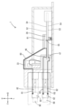
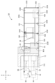
- FIG. 1 is a plan view of the connector device (excluding the cover member) of the first embodiment.
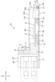
- FIG. 2 is a cross-sectional view taken along line AA in FIG.
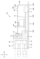
- FIG. 3 is a sectional view taken along line BB in FIG.
- FIG. 4 is an explanatory diagram conceptually showing a route for transmitting heat from the IC to the shield layer in the first embodiment.
- FIG. 5 is an explanatory diagram conceptually showing a path for transmitting heat from the IC to the main ground circuit in the first embodiment.
- FIG. 6 is a diagram corresponding to FIG. 3 of the second embodiment.
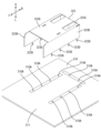
- FIG. 7 is an exploded perspective view of a circuit board, a cover member, and a mounting member in the second embodiment.
- FIG. 8 is an explanatory diagram conceptually showing a route for transmitting IC heat to the shield layer and a route for transmitting IC heat to the main ground circuit in the second embodiment.
- FIG. 9 is a diagram corresponding to FIG. 3 of the third embodiment.
- FIG. 10 is an exploded perspective view of a circuit board and a mounting cover member in Embodiment 3.
- FIG. 11 is an explanatory diagram conceptually showing a route for transmitting IC heat to the shield layer and a route for transmitting IC heat to the main ground circuit in the third embodiment.
- the connector device of the present disclosure includes a circuit board and a connector installed on the circuit board, and the connector includes an outer conductor that can conduct with a shield layer of a shielded wire, a sub-board, and the sub-board.
- the device includes an IC mounted on a substrate and a heat transfer section that transfers heat from the IC to the shield layer.
- the heat of the IC can be transferred to the shield layer of the shielded wire via the heat transfer part, so that the heat of the IC can be easily dissipated.
- the heat transfer section has an outer conductor heat transfer section that transfers heat of the IC to the outer conductor, and the heat transfer section transmits the heat of the IC to the outer conductor through the outer conductor heat transfer section and the outer conductor. Heat from the IC may be transferred to the shield layer.
- the heat of the IC can be released to the shield layer using the outer conductor.
- the outer conductor heat transfer section may include a metal plate.
- the heat transfer efficiency of the outer conductor heat transfer section can be improved.
- the outer conductor heat transfer part has a first contact part that contacts a surface of the IC opposite to the sub-board, and a contact position with the IC. It may have a second contact part that contacts the outer conductor at a height different from that of the second contact part, and a step part that connects the first contact part and the second contact part in a step shape.
- the parts of the IC and the outer conductor that are at different heights can be connected by the heat transfer part for the outer conductor.
- the outer conductor heat transfer section may be constituted by a sub-ground circuit provided on the sub-board.
- the sub-ground circuit has a sub-extension circuit
- the outer conductor has an overhang that protrudes in the direction in which the sub-extension circuit to be contacted extends
- the The projecting portion may be configured to contact the sub-extension circuit
- the outer conductor may have a regulating portion disposed on a side opposite to the overhang portion with respect to the sub-board.
- the regulating portion can restrict the sub-board from separating from the overhanging portion, it is easy to maintain the contact state between the overhanging portion and the sub-extension circuit.
- the heat transfer section may also transfer the heat of the IC to a main ground circuit provided on the circuit board.
- the heat of the IC can also be released to the main ground circuit via the heat transfer section.
- the sub-board and the IC may be arranged on one side of the circuit board in the thickness direction.
- the connector may include a conductive cover member installed to cover the sub-board and the IC from the one side in the thickness direction.
- the heat transfer section includes a cover heat transfer section that transfers the heat of the IC to the cover member, and transfers the heat of the IC to the main ground circuit via the cover heat transfer section and the cover member. Good too.
- the heat of the IC can be released to the main ground circuit using the cover member.
- the connector may have a conductive mounting member mounted on the main ground circuit.
- the cover member may be removably attached to the attachment member.
- the heat of the IC can be released to the main ground circuit by the cover heat transfer section, the cover member, and the mounting member. Moreover, the cover member can be attached to and detached from the circuit board.
- the circuit board and the sub-board may be arranged such that their plate surfaces face each other.
- the sub-board may be provided with a sub-ground circuit arranged to face the main ground circuit provided on the circuit board.
- the IC may be connected to the sub-ground circuit.
- a conductive member may be provided between the sub-ground circuit and the main ground circuit. The conductive member may enable conduction between the sub-ground circuit and the main ground circuit.
- the connector device of (11) has a configuration in which at least a portion of the main ground circuit and at least a portion of the sub-ground circuit are opposed to each other, and a conductive member is disposed between the opposing portions. Good to have.
- the connector device of (11) may have a configuration in which the entire main ground circuit and the entire sub-ground circuit face each other, or the entire main ground circuit and only a part of the sub-ground circuit face each other.
- It may be a configuration in which only a part of the main ground circuit and the entire sub-ground circuit face each other, or a configuration in which only a part of the main ground circuit and only a part of the sub-ground circuit face each other. A configuration in which they face each other may also be used.
- the connector may have a mounting part that is mounted on the circuit board and holds the sub-board.
- the conductive member may bias the circuit board and the sub-board so that they are spaced apart from each other in a direction in which their plate surfaces face each other.
- the conductive member is pressed against the main ground circuit of the circuit board and the sub-ground circuit of the sub-board while the sub-board is held by the mounting portion so as not to separate from the circuit board.
- the state of contact with the ground circuit and main ground circuit is likely to be stable.
- the connector may include a conductive mounting cover member that covers the sub-board and the IC and is mounted on the main ground circuit.
- the heat transfer section has a mounting cover heat transfer section that transfers the heat of the IC to the mounting cover member, and the heat transfer section for mounting cover and the mounting cover member transfer the heat of the IC to the main ground circuit. You can also tell them.
- the heat of the IC can be released to the main ground circuit using the mounting cover member.
- the connector may include an inner conductor and an outer conductor that covers the outer periphery of the inner conductor.
- the outer conductor may be placed on the main ground circuit.
- the heat transfer section includes an outer conductor heat transfer section that transfers the heat of the IC to the outer conductor, and the outer conductor heat transfer section and the outer conductor transfer the heat of the IC to the main ground circuit. It's okay.
- the heat of the IC can be released to the main ground circuit using the outer conductor.
- FIG. 1 shows a connector device 1 according to a first embodiment.
- the connector device 1 is mounted on a vehicle, for example.
- FIG. 1 shows the connector device 1 with a cover member 23 (see FIG. 2), which will be described later, removed.
- the connector device 1 includes a circuit board 10 and a connector 20 installed on the circuit board 10.
- the connector 20 is fitted with a mating connector 80, as shown in FIG.
- the side on which the connector 20 is installed with respect to the circuit board 10 is defined as the upper side.
- the side on which the mating connector 80 is fitted to the connector 20 is defined as the front side.
- a direction perpendicular to the up-down direction and the front-back direction is defined as the width direction.
- upper, lower, front, and rear are respectively expressed as "U,”"L,”"F,” and "B.”
- the circuit board 10 has a plate shape.
- the board thickness direction of the circuit board 10 is an up-down direction, and is a direction perpendicular to the board surface of the circuit board 10.
- the circuit board 10 has a board body 11 and a main ground circuit 12, as shown in FIG.
- the substrate body 11 has a plate shape.
- the substrate body 11 has insulating properties and is made of resin, for example.
- a mounting surface 13 is formed on the board body 11 .
- the mounting surface 13 is formed on the upper surface of the board body 11.
- the main ground circuit 12 is provided on the circuit board 10 (more specifically, the mounting surface 13).
- the main ground circuit 12 is exposed on the mounting surface 13 of the circuit board 10.
- the main ground circuit 12 has an extension circuit 14 extending in the front-rear direction along the mounting surface 13.
- a plurality of extension circuits 14 are provided at intervals in the width direction.
- the connector 20 is a board connector installed on the circuit board 10, as shown in FIG.
- the connector 20 includes a mounting connector section 21 mounted on the circuit board 10, a relay connector section 22 connected to the mounting connector section 21, and a cover member 23.
- the mounting connector section 21 corresponds to an example of a "mounting section". As shown in FIG. 2, the mounting connector section 21 is configured as, for example, a card edge connector. A relay connector section 22 is detachably connected to the mounting connector section 21 . An opening is formed in the front surface of the mounting connector section 21. By inserting the relay connector part 22 into this opening from the front, the relay connector part 22 is connected to the mounting connector part 21.
- the relay connector section 22 is detachably connected to the mounting connector section 21.
- the relay connector section 22 is connected to the mounting connector section 21 and the mating connector 80.
- the relay connector section 22 functions as an adapter.
- a plurality of types of relay connector sections 22 are prepared in advance, depending on, for example, the number of devices mounted on the vehicle and communication specifications (for example, communication speed, etc.). By connecting the relay connector section 22 to the mounting connector section 21 according to the specifications of the vehicle in which the connector device 1 is mounted, the connector device 1 becomes compatible with a plurality of types of vehicles.
- the relay connector section 22 includes a fitting member 31, an inner conductor 32, an outer conductor 33, a dielectric 34, a sub-board 35, an IC 36, and a relay section 37. ing.
- the fitting member 31 fits into the mating connector 80, as shown in FIG.
- the fitting member 31 has insulation properties and is made of resin, for example.
- the fitting member 31 has a rectangular cylindrical hood portion 31A and a rear wall portion 31B that covers the rear surface of the hood portion 31A.
- the inner conductor 32 has a shape extending in the front-rear direction.
- a plurality of inner conductors 32 are provided at intervals in a direction orthogonal to the front-rear direction.
- the front end of the inner conductor 32 protrudes into the hood portion 31A, and the rear end of the inner conductor 32 protrudes to the rear of the rear wall portion 31B.
- the inner conductor 32 is electrically connected to the core wire 91 of the shielded wire 90 when the connector 20 and the mating connector 80 are fitted together.
- the inner conductor 32 is electrically connected to the mating inner conductor 81 of the mating connector 80 .
- a core wire 91 is electrically connected to the mating inner conductor 81 . That is, the inner conductor 32 is electrically connected to the core wire 91 via the counterpart inner conductor 81.
- the inner conductor 32 is electrically connected to the conductive path of the sub-board 35 via the relay portion 37 .
- the outer conductor 33 covers the outer periphery of the inner conductor 32, as shown in FIG.
- the outer conductor 33 has a wall portion 40 that is thick in the front-rear direction.
- the wall portion 40 is formed with an insertion hole 41 through which the inner conductor 32 is inserted.
- the outer conductor 33 has a cylindrical portion 42 that projects forward from the outer periphery of the insertion hole 41 in a cylindrical shape.
- the cylinder portion 42 penetrates the rear wall portion 31B of the fitting member 31 and projects into the hood portion 31A.
- the outer conductor 33 is electrically connected to the shield layer 92 of the shielded wire 90 when the connector 20 and the mating connector 80 are fitted together.
- the outer conductor 33 is electrically connected to the mating outer conductor 82 by fitting the mating outer conductor 82 of the mating connector 80 into the cylindrical portion 42 .
- a shield layer 92 is electrically connected to the mating outer conductor 82 . That is, the outer conductor 33 is electrically connected to the shield layer 92 via the counterpart outer conductor 82.
- the outer conductor 33 has an upper wall portion 43 that extends rearward from the upper end side of the wall portion 40.
- the outer conductor 33 has a bottom wall portion 44 that extends rearward from the lower end side of the wall portion 40 .
- the outer conductor 33 has a fixing portion 45 that protrudes outward in the width direction.
- the fixing portion 45 is fixed to the circuit board 10 with screws or the like.
- the outer conductor 33 is installed on the main ground circuit 12 and is electrically connected to the main ground circuit 12.
- the outer conductor 33 is fixed to the circuit board 10 by the fixing portion 45, thereby making the contact state with the main ground circuit 12 more stable.
- the outer conductor 33 has an overhanging portion 46 and a restricting portion 47 that project rearward at a position rearward of the wall portion 40.
- the projecting portion 46 and the regulating portion 47 are arranged at intervals from each other in the vertical direction.
- the sub-board 35 is arranged in the gap between the overhanging part 46 and the regulating part 47.
- the sub-board 35 is in contact with the protruding portion 46 and the regulating portion 47 and is sandwiched between the upper and lower sides.
- the projecting portion 46 is located above the regulating portion 47.
- the projecting portion 46 and the regulating portion 47 are respectively arranged on both sides of the outer conductor 33 in the width direction.
- the sub-board 35 is arranged in the gap between the overhanging part 46 and the regulating part 47 on both sides of the outer conductor 33 in the width direction.
- the dielectric 34 is arranged between the inner conductor 32 and the outer conductor 33, as shown in FIG.
- the sub-board 35 has a plate shape.
- the thickness direction of the sub-board 35 is a vertical direction, a direction perpendicular to the board surface of the sub-board 35, and a direction in which the circuit board 10 and the sub-board 35 are arranged.
- the sub-board 35 is a board built into the connector 20, as shown in FIG.
- the sub-board 35 is detachably connected to the mounting connector section 21.
- the sub-board 35 is capable of communicating with the circuit board 10 via the mounting connector section 21.
- the sub-board 35 is arranged at a position above the circuit board 10.
- the sub-board 35 and the circuit board 10 are arranged such that their board surfaces face each other in the vertical direction.
- the lower surface of the sub-board 35 faces the upper surface of the circuit board 10.
- the sub-board 35 has a sub-board main body 51 and a sub-ground circuit 52.
- the sub-board main body 51 has a plate shape.
- the sub-board main body 51 has insulating properties and is made of resin, for example.
- a sub-mounting surface 53 is formed on the sub-board main body 51.
- the sub-mounting surface 53 is formed on the upper surface of the sub-board main body 51.
- the sub-ground circuit 52 is provided on the sub-board 35 (more specifically, on the sub-mounting surface 53), as shown in FIGS. 1 and 3.
- the IC 36 (more specifically, the lead wire of the IC 36) is electrically connected to the sub-ground circuit 52.
- the sub-ground circuit 52 is exposed on the sub-mounting surface 53 of the sub-board 35.
- the sub-ground circuit 52 has a sub-extension circuit 54 extending in the front-rear direction along the sub-mounting surface 53.
- a plurality of sub-extension circuits 54 are provided at intervals in the width direction.
- the sub-extension circuit 54 is provided on both the upper and lower surfaces of the sub-board 35.
- the sub-extension circuits 54 on both the upper and lower surfaces are electrically connected via vias 55 that penetrate the sub-board main body 51 in the thickness direction.
- the sub-extension circuit 54 on the upper surface comes into contact with the lower surface of the overhanging part 46 (more specifically, The sub-extension circuit 54 on the lower surface contacts the upper surface of the regulating portion 47 (more specifically, surface contact). That is, the IC 36 is electrically connected to the outer conductor 33 via the sub-ground circuit 52.
- the IC 36 is mounted on the sub-mounting surface 53 (upper surface) of the sub-board 35.
- the relay connector section 22 includes a metal plate 60 and a heat dissipation sheet 61.
- the metal plate 60 is bonded to the upper surface of the upper wall portion 43 of the outer conductor 33, and is bonded to the upper surface of the IC 36 via the heat dissipation sheet 61.
- the metal plate 60 and the heat dissipation sheet 61 have a first contact portion 62 that contacts (more specifically, surface contact with) the upper surface of the IC 36, and a first contact portion 62 that contacts the outer conductor 33 (more specifically, contacts with the outer conductor 33 at a height position different from the upper surface of the IC 36).
- the second contact part 63 makes surface contact (surface contact), and the step part 64 connects the first contact part 62 and the second contact part 63 in a step shape.
- the relay connector section 22 has a conductive member 70.
- the main ground circuit 12 and the sub-ground circuit 52 described above are arranged vertically facing each other.
- the conductive member 70 is arranged between the main ground circuit 12 and the sub-ground circuit 52, which are arranged to face each other, and is electrically connected to the main ground circuit 12 and the sub-ground circuit 52.
- the conductive member 70 guides the contact conductive part 71 in contact with the sub-ground circuit 52, the biasing member 72 disposed between the contact conductive part 71 and the main ground circuit 12, and the contact conductive part 71 in the vertical direction. It has a guide part 73.
- the contact conductive portion 71 is formed with an inclined surface 71A that slopes downward toward the front end.
- the contact conductive portion 71 moves downward when the inclined surface 71A is pressed from the front by the sub-board 35.
- the biasing member 72 is, for example, a spring member, and biases the contact conductive portion 71 in a direction away from the main ground circuit 12 .
- the sub-board 35 is held by the mounting connector section 21, and its movement in the direction away from the circuit board 10 (more specifically, upward) is restricted. Therefore, the conductive member 70 is pressed against the main ground circuit 12 and the sub-ground circuit 52.
- the cover member 23 covers the sub-board 35 and the IC 36 from above, as shown in FIG.
- the cover member 23 is fixed to the circuit board 10 with screws or the like.
- the connector device 1 can release the heat of the IC 36 to the shield layer 92 of the shield wire 90 in the following manner.
- the connector device 1 can release the heat of the IC 36 to the shield layer 92 by using the outer conductor 33.
- the heat of the IC 36 is transmitted to the outer conductor 33 via the metal plate 60, so that the heat transfer efficiency can be improved.
- the heat transfer efficiency from the IC 36 to the heat dissipation sheet 61 can be improved. Since the metal plate 60 is in surface contact with the heat dissipation sheet 61, the efficiency of heat transfer from the heat dissipation sheet 61 to the metal plate 60 can be improved. Since the metal plate 60 is in surface contact with the outer conductor 33, the heat transfer efficiency from the metal plate 60 to the outer conductor 33 can be improved. That is, in the route R1, the heat transfer efficiency from the IC 36 to the outer conductor 33 can be improved.
- the metal plate 60 and the heat dissipation sheet 61 have a first contact portion 62 that contacts the top surface of the IC 36 (more specifically, surface contact), and a first contact portion 62 that contacts the outer conductor 33 at a height position different from the top surface of the IC 36 ( More specifically, it includes a second contact portion 63 that makes surface contact (surface contact), and a stepped portion 64 that connects the first contact portion 62 and the second contact portion 63 in a stepped manner. Therefore, the surfaces of the IC 36 and the outer conductor 33 having different height positions can be connected by the metal plate 60 and the heat dissipation sheet 61.
- the "height position” is a position in the vertical direction (direction perpendicular to the sub-mounting surface 53) with respect to the sub-mounting surface 53 of the sub-board 35.
- the connector device 1 can release the heat of the IC 36 to the shield layer 92 via the sub-extension circuit 54 on the top surface and the outer conductor 33, as shown in path R2 shown in FIG. Furthermore, the connector device 1 can release the heat of the IC 36 to the shield layer 92 via the via 55, the sub-extension circuit 54 on the lower surface, and the outer conductor 33, as shown in path R3 shown in FIG.
- the connector device 1 can release the heat of the IC 36 to the shield layer 92 by using the outer conductor 33.
- the connector device 1 can ensure a heat transfer path from the IC 36 to the outer conductor 33 while reducing the size of the connector device 1 by using the paths R2 and R3.
- the outer conductor 33 has a projecting portion 46 that projects rearward.
- the lower surface of the projecting portion 46 is in contact (more specifically, surface contact) with the sub-extension circuit 54 extending in the front-rear direction on the route R2. Therefore, in the connector device 1, it is easy to increase the contact area between the outer conductor 33 and the sub-ground circuit 52, and therefore it is easy to improve the heat transfer efficiency.
- the outer conductor 33 has a restriction portion 47 arranged on the side opposite to the overhang portion 46 side with respect to the sub-board 35 .
- the restriction portion 47 since the regulating portion 47 can restrict the sub-board 35 from separating from the overhang portion 46, it is easy to maintain the contact state between the overhang portion 46 and the sub-extension circuit 54.
- the restriction portion 47 also protrudes rearward, and the upper surface of the restriction portion 47 is in contact (more specifically, surface contact) with the sub-extension circuit 54 extending in the front-rear direction on the route R3. Therefore, in the connector device 1, it is easy to increase the contact area between the outer conductor 33 and the sub-ground circuit 52 on both sides of the sub-board 35, and therefore it is easy to improve heat transfer efficiency.
- the connector device 1 can release the heat of the IC 36 to the main ground circuit 12 in the following manner.
- route R11 As mentioned above in the description of the route R1, the heat of the IC 36 is transmitted to the outer conductor 33 by the heat dissipation sheet 61 and the metal plate 60. Further, the outer conductor 33 is electrically connected to the main ground circuit 12. Therefore, the connector device 1 can release the heat of the IC 36 to the main ground circuit 12 via the heat dissipation sheet 61, the metal plate 60, and the outer conductor 33, as shown in the path R11 shown in FIG.
- the connector device 1 can release the heat of the IC 36 to the main ground circuit 12 by using the outer conductor 33.
- the connector device 1 can release the heat of the IC 36 to the main ground circuit 12 via the sub-extension circuit 54 on the top surface and the outer conductor 33, as shown in the path R12 shown in FIG. Further, the connector device 1 can release the heat of the IC 36 to the main ground circuit 12 via the via 55, the sub-extension circuit 54 on the lower surface, and the outer conductor 33, as shown in the path R13 shown in FIG. Also in these paths R12 and R13, the connector device 1 can release the heat of the IC 36 to the main ground circuit 12 by using the outer conductor 33.
- the sub-ground circuit 52 is electrically connected to the main ground circuit 12 via a conductive member 70. Therefore, the connector device 1 can release the heat of the IC 36 to the main ground circuit 12 via the sub-ground circuit 52 and the conductive member 70, as shown in the path R14 shown in FIG.
- the connector device 1 enables conduction between the sub-ground circuit 52 and the main ground circuit 12 that face each other through the conductive member 70, the heat transfer path for transmitting the heat of the IC 36 to the main ground circuit 12 can be shortened. .
- the sub-board 35 is held by the mounting connector part 21, and the conductive member 70 urges the circuit board 10 and the sub-board 35 to be separated from each other in a direction in which their plate surfaces face each other.
- the sub-board 35 is held by the mounting connector portion 21 so as not to separate from the circuit board 10, and the conductive member 70 is connected to the main ground circuit 12 of the circuit board 10 and the sub-ground circuit 52 of the sub-board 35. Since it is pressed, the contact state between the conductive member 70 and the sub-ground circuit 52 and the main ground circuit 12 is likely to be stabilized.
- the direction in which the plate surfaces face each other is the direction in which the main ground circuit 12 and the sub-ground circuit 52 face each other. Further, "the direction in which the plate surfaces face each other” is a direction perpendicular to the direction in which the connector 20 and the mating connector 80 are fitted.
- the connector device 1 can release the heat of the IC 36 to the main ground circuit 12 via the mounting connector section 21, as shown in paths R15 and R16 shown in FIG.
- Embodiment 2 In Embodiment 2, an example will be described in which heat is radiated using a cover member. Note that the same components as in Embodiment 1 are given the same reference numerals, and detailed explanations are omitted.
- FIG. 6 shows a connector device 201 according to a second embodiment.
- the connector device 201 is mounted on a vehicle, for example.
- the connector device 201 includes a circuit board 10 and a connector 220 installed on the circuit board 10.
- the connector 220 is a board connector installed on the circuit board 10, as shown in FIG.
- the connector 220 includes a mounting connector section 21, a relay connector section 222 connected to the mounting connector section 21, a cover member 223, and a mounting member 270.
- the relay connector section 222 includes a fitting member 31, an inner conductor 32, an outer conductor 33, a dielectric 34, a sub-board 35, an IC 36, and a relay section 37. ing.
- the relay connector section 222 has a heat dissipation sheet 260, as shown in FIG.
- the heat dissipation sheet 260 is installed on the top surface of the IC 36.
- the cover member 223 has electrical conductivity and is configured as, for example, a metal casing.
- the cover member 223 covers the sub-board 35 and the IC 36, as shown in FIG.
- the cover member 223 is fixed to the circuit board 10 with screws or the like.
- the cover member 223 has a top plate portion 223A, a pair of side plate portions 223B, and a rear plate portion 223C.
- the pair of side plate portions 223B are arranged at intervals in the width direction. Both end portions of the top plate portion 223A in the width direction are connected to upper end portions of the pair of side plate portions 223B.
- the rear plate portion 223C is continuous with the rear end portions of the top plate portion 223A and the pair of side plate portions 223B.
- the lower surface and front surface of the cover member 223 are open.
- the cover member 223 is arranged with the top plate portion 223A in contact with the upper surface of the heat dissipation sheet 260. Further, the cover member 223 is arranged with the top plate portion 223A in contact with the rear surface of the outer conductor 33. Further, the cover member 223 is fixed to the circuit board 10 using a mounting member 270.
- the main ground circuit 12 includes an extended circuit 14A extending in the front-rear direction along the mounting surface 13, and an extended circuit 14B extending in the width direction.
- the extended circuits 14A and 14B are arranged corresponding to the position of the lower end of the cover member 223.
- a plurality of mounting members 270 are mounted on the extended circuits 14A and 14B.
- the mounting member 270 is electrically conductive and is made of metal, for example.
- the mounting member 270 includes a plate-shaped base portion 271 that is fixed onto the extended circuits 14A and 14B, and a holding portion 272 that extends upward from both sides of the base portion 271 in a cantilever shape to sandwich the cover member 223. have.
- the minimum interval between the holding parts 272 is smaller than the thickness of the pair of side plate parts 223B and smaller than the thickness of the rear plate part 223C.
- the cover member 223 is attached to the attachment member 270 by pushing the holding portion 272 apart from above.
- the cover member 223 is removable from the attachment member 270.
- the connector device 201 can release the heat of the IC 36 to the shield layer 92 of the shield wire 90 in the following manner.
- the heat of the IC 36 is transferred to the outer conductor 33 by the heat dissipation sheet 260 and the cover member 223.
- the outer conductor 33 is electrically connected to the shield layer 92 . Therefore, the connector device 201 can release the heat of the IC 36 to the shield layer 92 via the heat dissipation sheet 260, the cover member 223, and the outer conductor 33, as shown in path R4 shown in FIG. That is, the connector device 201 can release the heat of the IC 36 to the shield layer 92 by using the cover member 223.
- the connector device 201 can also release the heat of the IC 36 to the shield layer 92 like the paths R2 and R3 shown in FIG. 4, as in the first embodiment.
- the connector device 201 can release the heat of the IC 36 to the main ground circuit 12 in the following manner.
- the connector device 201 can release the heat of the IC 36 to the main ground circuit 12 via the heat dissipation sheet 260, the cover member 223, and the outer conductor 33, as shown in the path R17 shown in FIG. That is, the connector device 201 can release the heat of the IC 36 to the main ground circuit 12 using the cover member 223.
- the connector device 201 can release the heat of the IC 36 to the main ground circuit 12 through the heat dissipation sheet 260, the cover member 223, and the mounting member 270, as shown in the path R18 shown in FIG. That is, the connector device 201 can release the heat of the IC 36 to the main ground circuit 12 using the cover member 223.
- the cover member 223 can be attached to and detached from the circuit board 10.
- the connector device 201 can also release the heat of the IC 36 to the main ground circuit 12 like the routes R12, R13, R15, and R16 shown in FIG. 5, as in the first embodiment.
- Embodiment 3 In Embodiment 3, an example will be described in which heat is radiated using a mounting cover member mounted on a circuit board. Note that the same components as in Embodiment 1 are given the same reference numerals, and detailed explanations are omitted.
- FIG. 9 shows a connector device 301 according to a third embodiment.
- the connector device 301 is mounted on a vehicle, for example.
- the connector device 301 includes a circuit board 310 and a connector 320 installed on the circuit board 310.
- the circuit board 310 includes a board body 311 and a main ground circuit 12.
- a through hole 310A is formed in the board body 311 for mounting a mounting cover member 323, which will be described later.
- the substrate body 311 is the same as the substrate body 11 of the first embodiment in other respects.
- the connector 320 is a board connector installed on the circuit board 310, as shown in FIG.
- the connector 320 includes a mounting connector section 21, a relay connector section 322 connected to the mounting connector section 21, and a mounting cover member 323.
- the relay connector section 322 includes a fitting member 31, an inner conductor 32, an outer conductor 33, a dielectric 34, a sub-board 35, an IC 36, and a relay section 37. ing.
- the relay connector section 322 has heat radiation fins 360, as shown in FIG.
- the radiation fin 360 is installed on the upper surface of the IC 36.
- the mounting cover member 323 has conductivity and is made of metal, for example.
- the mounting cover member 323 covers the sub-board 35 and the IC 36 and is mounted on the main ground circuit 12 of the circuit board 310, as shown in FIG.
- the mounting cover member 323 has a top plate portion 323A, a pair of side plate portions 323B, a rear plate portion 323C, and a plurality of leg portions 323D.
- the pair of side plate portions 323B are arranged at intervals in the width direction. Both end portions of the top plate portion 323A in the width direction are connected to upper end portions of the pair of side plate portions 323B.
- the rear plate portion 323C is continuous with the rear end portions of the top plate portion 323A and the pair of side plate portions 323B.
- the leg portions 323D protrude downward from the lower ends of the pair of side plate portions 323B and rear plate portion 323C.
- the lower and front surfaces of the mounting cover member 323 are open.
- the mounting cover member 323 has a holding protrusion 323E.
- the holding protrusion 323E projects downward from the top plate portion 323A.
- the holding protrusion 323E is arranged in contact with the upper end of the heat radiation fin 360.
- the mounting cover member 323 is arranged with the top plate portion 323A in contact with the rear surface of the outer conductor 33.
- the above-described through hole 310A is arranged at a position corresponding to the leg portion 323D of the mounting cover member 323, as shown in FIG. Furthermore, the through hole 310A is electrically connected to the main ground circuit 12.
- the mounting cover member 323 is mounted on the circuit board 310 with the legs 323D inserted into the through holes 310A. Thereby, the mounting cover member 323 is electrically connected to the main ground circuit 12.
- the connector device 301 can release the heat of the IC 36 to the shield layer 92 of the shield wire 90 in the following manner.
- the heat of the IC 36 is transferred to the outer conductor 33 by the radiation fins 360 and the mounting cover member 323.
- the outer conductor 33 is electrically connected to the shield layer 92 . Therefore, the connector device 301 can release the heat of the IC 36 to the shield layer 92 via the radiation fins 360, the mounting cover member 323, and the outer conductor 33, as shown in the path R5 shown in FIG. That is, the connector device 301 can release the heat of the IC 36 to the shield layer 92 by using the mounting cover member 323.
- the connector device 301 can also release the heat of the IC 36 to the shield layer 92 like the paths R2 and R3 shown in FIG. 4, as in the first embodiment.
- the connector device 301 can release the heat of the IC 36 to the main ground circuit 12 in the following manner.
- the connector device 301 can release the heat of the IC 36 to the main ground circuit 12 via the radiation fins 360, the mounting cover member 323, and the outer conductor 33, as shown in the path R19 shown in FIG. That is, the connector device 301 can release the heat of the IC 36 to the main ground circuit 12 by using the mounting cover member 323.
- the connector device 301 can release the heat of the IC 36 to the main ground circuit 12 through the radiation fins 360 and the mounting cover member 323, as shown in the path R20 shown in FIG. In other words, the connector device 301 can release the heat of the IC 36 to the main ground circuit 12 by using the mounting cover member 323 also in the route R20.
- the connector device 301 can also release the heat of the IC 36 to the main ground circuit 12 like the paths R12, R13, R15, and R16 shown in FIG. 5, as in the first embodiment.
- the connector has a configuration in which the mounting connector part and the relay connector part are separate from each other, but the connector may have a configuration in which the mounting connector part and the relay connector part are integrated.
- the heat of the IC is dissipated to the shield layer through the outer conductor, but it may be dissipated without using the outer conductor.
- the overhang portion is configured to protrude rearward (in the direction in which the mating connector is fitted to the connector), and the sub-extension circuit to be contacted by the overhang portion is in the front-rear direction (
- the structure extends in the direction in which the connector and the mating connector are fitted together, the structure is not limited to this.
- the projecting portion may be configured to protrude in the width direction (a direction perpendicular to the mating direction of the connector and the mating connector), and the sub-extension circuit to be contacted by the projecting portion may be configured to extend in the width direction. It's okay.
- Connector device 10 Circuit board 11: Board body 12: Main ground circuit 13: Mounting surface 14: Extension circuit 14A: Extension circuit 14B: Extension circuit 20: Connector 21: Mounting connector section 22: Relay connector section 23 : Cover member 31 : Fitting member 31A : Hood part 31B : Rear wall part 32 : Inner conductor 33 : Outer conductor (heat transfer part) 34: Dielectric 35: Sub board 36: IC 37 : Relay part 40 : Wall part 41 : Insertion hole 42 : Cylindrical part 43 : Top wall part 44 : Bottom wall part 45 : Fixing part 46 : Overhanging part 47 : Regulating part 51 : Sub-board body 52 : Sub-ground circuit ( Heat transfer part, heat transfer part for outer conductor) 53: Sub-mounting surface 54: Sub-extension circuit (heat transfer section, heat transfer section for outer conductor) 55: Via (heat transfer part, heat transfer part for outer conductor) 60: Metal plate (heat transfer part, heat transfer part for outer conductor
Landscapes
- Physics & Mathematics (AREA)
- Thermal Sciences (AREA)
- Engineering & Computer Science (AREA)
- Microelectronics & Electronic Packaging (AREA)
- Coupling Device And Connection With Printed Circuit (AREA)
- Details Of Connecting Devices For Male And Female Coupling (AREA)
- Cooling Or The Like Of Electrical Apparatus (AREA)
Abstract
Description
最初に本開示の実施態様を列記して説明する。
本開示の具体例を、以下に図面を参照しつつ説明する。なお、本発明はこれらの例示に限定されるものではなく、請求の範囲によって示され、請求の範囲と均等の意味および範囲内でのすべての変更が含まれることが意図される。
(コネクタ装置1の構成)
図1には、実施形態1のコネクタ装置1が開示されている。コネクタ装置1は、例えば車両に搭載される。図1では、後述するカバー部材23(図2参照)が取り外された状態のコネクタ装置1が示されている。コネクタ装置1は、回路基板10と、回路基板10に設置されるコネクタ20と、を備えている。コネクタ20は、図2に示すように、相手側コネクタ80と嵌合する。本実施形態において、回路基板10に対してコネクタ20が設置される側を上側と定義する。コネクタ20に対して相手側コネクタ80が嵌合される側を前側と定義する。上下方向及び前後方向と直交する方向を幅方向と定義する。図面においては、上方、下方、前方、後方をそれぞれ「U」「L」「F」「B」と表記する。
コネクタ装置1は、以下のようにして、IC36の熱をシールド電線90のシールド層92に逃がすことができる。
IC36の熱は、放熱シート61及び金属板60によって外導体33に伝えられる。上述したように、外導体33は、シールド層92と導通している。このため、コネクタ装置1は、図4に示す経路R1のように、IC36の熱を、放熱シート61、金属板60、及び外導体33を介してシールド層92に逃がすことができる。
また、IC36の熱は、サブ基板35の上下両面のサブ延設回路54によって外導体33に伝えられる。上述したように、外導体33は、シールド層92と導通している。このため、コネクタ装置1は、図4に示す経路R2のように、IC36の熱を、上面のサブ延設回路54及び外導体33を介してシールド層92に逃がすことができる。また、コネクタ装置1は、図4に示す経路R3のように、IC36の熱を、ビア55、下面のサブ延設回路54及び外導体33を介してシールド層92に逃がすことができる。
経路R1の説明で上述したように、IC36の熱は、放熱シート61及び金属板60によって外導体33に伝えられる。また、外導体33は、メイングランド回路12に電気的に接続されている。このため、コネクタ装置1は、図5に示す経路R11のように、IC36の熱を、放熱シート61、金属板60、及び外導体33を介してメイングランド回路12に逃がすことができる。
経路R2、R3の説明で上述したように、IC36の熱は、サブ基板35の上下両面のサブ延設回路54によって外導体33に伝えられる。また、外導体33は、メイングランド回路12に電気的に接続されている。このため、コネクタ装置1は、図5に示す経路R12のように、IC36の熱を、上面のサブ延設回路54、及び外導体33を介してメイングランド回路12に逃がすことができる。また、コネクタ装置1は、図5に示す経路R13のように、IC36の熱を、ビア55、下面のサブ延設回路54、及び外導体33を介してメイングランド回路12に逃がすことができる。この経路R12、R13においても、コネクタ装置1は、外導体33を利用して、IC36の熱をメイングランド回路12に逃がすことができる。
また、サブグランド回路52は、導電部材70を介してメイングランド回路12に電気的に接続されている。このため、コネクタ装置1は、図5に示す経路R14のように、IC36の熱を、サブグランド回路52、及び導電部材70を介してメイングランド回路12に逃がすことができる。
また、コネクタ装置1は、図5に示す経路R15、R16のように、IC36の熱を、実装コネクタ部21を介してメイングランド回路12に逃がすことができる。
実施形態2では、カバー部材を利用して放熱させる例について説明する。なお、実施形態1と同じ構成については同じ符号を付し、詳しい説明を省略する。
図6には、実施形態2のコネクタ装置201が開示されている。コネクタ装置201は、例えば車両に搭載される。コネクタ装置201は、回路基板10と、回路基板10に設置されるコネクタ220と、を備えている。
コネクタ装置201は、以下のようにして、IC36の熱をシールド電線90のシールド層92に逃がすことができる。
IC36の熱は、放熱シート260及びカバー部材223によって外導体33に伝えられる。外導体33は、シールド層92と導通している。このため、コネクタ装置201は、図8に示す経路R4のように、IC36の熱を、放熱シート260、カバー部材223、及び外導体33を介してシールド層92に逃がすことができる。つまり、コネクタ装置201は、カバー部材223を利用して、IC36の熱をシールド層92に逃がすことができる。
上述したように、IC36の熱は、放熱シート260及びカバー部材223によって外導体33に伝えられる。外導体33は、メイングランド回路12に電気的に接続されている。このため、コネクタ装置201は、図8に示す経路R17のように、IC36の熱を、放熱シート260、カバー部材223、及び外導体33を介してメイングランド回路12に逃がすことができる。つまり、コネクタ装置201は、カバー部材223を利用して、IC36の熱をメイングランド回路12に逃がすことができる。
更に、IC36の熱は、放熱シート260及びカバー部材223によって取付部材270に伝えられ、取付部材270を介してメイングランド回路12に伝えられる。このため、コネクタ装置201は、図8に示す経路R18のように、IC36の熱を、放熱シート260、カバー部材223、及び取付部材270によってメイングランド回路12に逃がすことができる。つまり、コネクタ装置201は、カバー部材223を利用して、IC36の熱をメイングランド回路12に逃がすことができる。しかも、カバー部材223が、回路基板10に対して着脱可能となる。
実施形態3では、回路基板に実装される実装カバー部材を利用して放熱させる例について説明する。なお、実施形態1と同じ構成については同じ符号を付し、詳しい説明を省略する。
図9には、実施形態3のコネクタ装置301が開示されている。コネクタ装置301は、例えば車両に搭載される。コネクタ装置301は、回路基板310と、回路基板310に設置されるコネクタ320と、を備えている。
コネクタ装置301は、以下のようにして、IC36の熱をシールド電線90のシールド層92に逃がすことができる。
IC36の熱は、放熱フィン360及び実装カバー部材323によって外導体33に伝えられる。外導体33は、シールド層92と導通している。このため、コネクタ装置301は、図11に示す経路R5のように、IC36の熱を、放熱フィン360、実装カバー部材323、及び外導体33を介してシールド層92に逃がすことができる。つまり、コネクタ装置301は、実装カバー部材323を利用して、IC36の熱をシールド層92に逃がすことができる。
上述したように、IC36の熱は、放熱フィン360及び実装カバー部材323によって外導体33に伝えられる。外導体33は、メイングランド回路12に電気的に接続されている。このため、コネクタ装置301は、図11に示す経路R19のように、IC36の熱を、放熱フィン360、実装カバー部材323、及び外導体33を介してメイングランド回路12に逃がすことができる。つまり、コネクタ装置301は、実装カバー部材323を利用して、IC36の熱をメイングランド回路12に逃がすことができる。
また、実装カバー部材323は、メイングランド回路12上に実装されている。このため、コネクタ装置301は、図11に示す経路R20のように、IC36の熱を、放熱フィン360、実装カバー部材323によってメイングランド回路12に逃がすことができる。つまり、コネクタ装置301は、経路R20においても、実装カバー部材323を利用して、IC36の熱をメイングランド回路12に逃がすことができる。
今回開示された実施の形態はすべての点で例示であって制限的なものではないと考えるべきである。
(1)上記各実施形態では、コネクタが、実装コネクタ部と中継コネクタ部とを互いに別体とした構成であったが、実装コネクタ部と中継コネクタ部とを一体とした構成であってもよい。
(2)上記各実施形態では、外導体を介してICの熱をシールド層に逃がす構成であったが、外導体を介さずに逃がす構成であってもよい。
(3)上記各実施形態では、張出部が後方(コネクタに対して相手側コネクタが嵌合する方向)に突出する構成であり、張出部の接触対象のサブ延設回路が前後方向(コネクタと相手側コネクタとの嵌合方向)に延びる構成であったが、この構成に限らない。例えば、張出部が幅方向(コネクタと相手側コネクタとの嵌合方向と直交する方向)に突出する構成であり、張出部の接触対象のサブ延設回路が幅方向に延びる構成であってもよい。
10 :回路基板
11 :基板本体
12 :メイングランド回路
13 :実装面
14 :延設回路
14A :延設回路
14B :延設回路
20 :コネクタ
21 :実装コネクタ部
22 :中継コネクタ部
23 :カバー部材
31 :嵌合部材
31A :フード部
31B :後壁部
32 :内導体
33 :外導体(伝熱部)
34 :誘電体
35 :サブ基板
36 :IC
37 :中継部
40 :壁部
41 :挿通孔
42 :筒部
43 :上壁部
44 :底壁部
45 :固定部
46 :張出部
47 :規制部
51 :サブ基板本体
52 :サブグランド回路(伝熱部、外導体用伝熱部)
53 :サブ実装面
54 :サブ延設回路(伝熱部、外導体用伝熱部)
55 :ビア(伝熱部、外導体用伝熱部)
60 :金属板(伝熱部、外導体用伝熱部)
61 :放熱シート(伝熱部、外導体用伝熱部)
62 :第1接触部
63 :第2接触部
64 :段差部
70 :導電部材(伝熱部)
71 :接触導電部
71A :傾斜面
72 :付勢部材
73 :ガイド部
80 :相手側コネクタ
81 :相手側内導体
82 :相手側外導体
90 :シールド電線
91 :芯線
92 :シールド層
201 :コネクタ装置
220 :コネクタ
222 :中継コネクタ部
223 :カバー部材(伝熱部、外導体用伝熱部)
223A :天板部
223B :側板部
223C :後板部
260 :放熱シート(伝熱部、外導体用伝熱部、カバー用伝熱部)
270 :取付部材(伝熱部)
271 :ベース部
272 :保持部
301 :コネクタ装置
310 :回路基板
310A :スルーホール
311 :基板本体
320 :コネクタ
322 :中継コネクタ部
323 :実装カバー部材(伝熱部、外導体用伝熱部)
323A :天板部
323B :側板部
323C :後板部
323D :脚部
323E :保持突起
360 :放熱フィン(伝熱部、外導体用伝熱部、実装カバー用伝熱部)
R1 :経路
R2 :経路
R3 :経路
R4 :経路
R5 :経路
R11 :経路
R12 :経路
R13 :経路
R14 :経路
R15 :経路
R16 :経路
R17 :経路
R18 :経路
R19 :経路
R20 :経路
Claims (8)
- 回路基板と、
前記回路基板に設置されるコネクタと、を備え、
前記コネクタは、シールド電線のシールド層と導通可能な外導体と、サブ基板と、前記サブ基板に実装されるICと、前記ICの熱を前記シールド層に伝える伝熱部と、を有しているコネクタ装置。 - 前記伝熱部は、前記ICの熱を前記外導体に伝える外導体用伝熱部を有し、前記外導体用伝熱部及び前記外導体を介して前記ICの熱を前記シールド層に伝える請求項1に記載のコネクタ装置。
- 前記外導体用伝熱部は、金属板を含む請求項2に記載のコネクタ装置。
- 前記外導体用伝熱部は、前記ICにおける前記サブ基板側とは反対側の面に接触する第1接触部と、前記ICとの接触位置とは異なる高さ位置において前記外導体に接触する第2接触部と、前記第1接触部と前記第2接触部とを段差状につなぐ段差部と、を有している請求項2又は請求項3に記載のコネクタ装置。
- 前記外導体用伝熱部は、前記サブ基板に設けられるサブグランド回路によって構成される請求項2に記載のコネクタ装置。
- 前記サブグランド回路は、サブ延設回路を有し、
前記外導体は、接触対象の前記サブ延設回路の延びる方向に突出する張出部を有し、
前記張出部は、前記サブ延設回路に接触する請求項5に記載のコネクタ装置。 - 前記外導体は、前記サブ基板に対し、前記張出部側とは反対側に配置される規制部を有している請求項6に記載のコネクタ装置。
- 前記伝熱部は、前記ICの熱を前記回路基板に設けられるメイングランド回路にも伝える請求項1又は請求項2に記載のコネクタ装置。
Priority Applications (2)
| Application Number | Priority Date | Filing Date | Title |
|---|---|---|---|
| CN202380046335.4A CN119301824A (zh) | 2022-06-29 | 2023-06-09 | 连接器装置 |
| US18/879,474 US20250226604A1 (en) | 2022-06-29 | 2023-06-09 | Connector device |
Applications Claiming Priority (2)
| Application Number | Priority Date | Filing Date | Title |
|---|---|---|---|
| JP2022104760A JP7788077B2 (ja) | 2022-06-29 | 2022-06-29 | コネクタ装置 |
| JP2022-104760 | 2022-06-29 |
Publications (1)
| Publication Number | Publication Date |
|---|---|
| WO2024004591A1 true WO2024004591A1 (ja) | 2024-01-04 |
Family
ID=89382871
Family Applications (1)
| Application Number | Title | Priority Date | Filing Date |
|---|---|---|---|
| PCT/JP2023/021572 Ceased WO2024004591A1 (ja) | 2022-06-29 | 2023-06-09 | コネクタ装置 |
Country Status (4)
| Country | Link |
|---|---|
| US (1) | US20250226604A1 (ja) |
| JP (1) | JP7788077B2 (ja) |
| CN (1) | CN119301824A (ja) |
| WO (1) | WO2024004591A1 (ja) |
Citations (4)
| Publication number | Priority date | Publication date | Assignee | Title |
|---|---|---|---|---|
| JP2001345151A (ja) * | 2000-03-31 | 2001-12-14 | Tyco Electronics Amp Kk | 電気コネクタ組立体および雌コネクタ |
| JP2007527095A (ja) * | 2003-06-13 | 2007-09-20 | エフシーアイ | シールドケージ |
| JP2014036033A (ja) * | 2012-08-07 | 2014-02-24 | Hitachi Automotive Systems Ltd | 半導体装置 |
| JP2019216022A (ja) * | 2018-06-13 | 2019-12-19 | ホシデン株式会社 | コネクタアッセンブリ、接続モジュール及び接続モジュールの製造方法 |
Family Cites Families (2)
| Publication number | Priority date | Publication date | Assignee | Title |
|---|---|---|---|---|
| JP4785962B2 (ja) | 2009-09-10 | 2011-10-05 | 日本航空電子工業株式会社 | コネクタ組立体 |
| US10104760B1 (en) | 2017-06-12 | 2018-10-16 | Te Connectivity Corporation | Pluggable module having cooling channel with heat transfer fins |
-
2022
- 2022-06-29 JP JP2022104760A patent/JP7788077B2/ja active Active
-
2023
- 2023-06-09 WO PCT/JP2023/021572 patent/WO2024004591A1/ja not_active Ceased
- 2023-06-09 CN CN202380046335.4A patent/CN119301824A/zh active Pending
- 2023-06-09 US US18/879,474 patent/US20250226604A1/en active Pending
Patent Citations (4)
| Publication number | Priority date | Publication date | Assignee | Title |
|---|---|---|---|---|
| JP2001345151A (ja) * | 2000-03-31 | 2001-12-14 | Tyco Electronics Amp Kk | 電気コネクタ組立体および雌コネクタ |
| JP2007527095A (ja) * | 2003-06-13 | 2007-09-20 | エフシーアイ | シールドケージ |
| JP2014036033A (ja) * | 2012-08-07 | 2014-02-24 | Hitachi Automotive Systems Ltd | 半導体装置 |
| JP2019216022A (ja) * | 2018-06-13 | 2019-12-19 | ホシデン株式会社 | コネクタアッセンブリ、接続モジュール及び接続モジュールの製造方法 |
Also Published As
| Publication number | Publication date |
|---|---|
| JP2024004882A (ja) | 2024-01-17 |
| CN119301824A (zh) | 2025-01-10 |
| JP7788077B2 (ja) | 2025-12-18 |
| US20250226604A1 (en) | 2025-07-10 |
Similar Documents
| Publication | Publication Date | Title |
|---|---|---|
| CN106684595B (zh) | 电连接器组件及使用该电连接器组件的电连接系统 | |
| CN201285827Y (zh) | 电连接器 | |
| US20140202755A1 (en) | Receptacle cage, receptacle assembly, and transceiver module assembly | |
| CN110299635A (zh) | 连接器以及电子设备 | |
| JP2009291044A (ja) | 電気接続箱 | |
| JP2012235693A (ja) | 電気接続箱 | |
| CN113410706B (zh) | 线缆连接器 | |
| CN102623814B (zh) | 端子和端子连接结构 | |
| JPH11329616A (ja) | コネクタ及びコネクタを用いた接続構造 | |
| WO2024004591A1 (ja) | コネクタ装置 | |
| CN113410715A (zh) | 连接器组件 | |
| JP7793132B2 (ja) | コネクタ装置 | |
| TWI763385B (zh) | 連接器組件 | |
| JP5565608B2 (ja) | 回路ユニット | |
| CN113422232B (zh) | 端子安装结构、线缆连接器及连接器组件 | |
| JP7442136B2 (ja) | 基板モジュール、接続システム及び基板 | |
| US7763796B2 (en) | Electric connection box and manufacturing method of electric connection box | |
| TWM629882U (zh) | 光電連接器 | |
| JP7163742B2 (ja) | 電気コネクタ | |
| CN120303837A (zh) | 连接器装置 | |
| TWI923293B (zh) | I/o連接器裝置 | |
| CN121584297A (zh) | 电连接器 | |
| WO2025177830A1 (ja) | 電気機器 | |
| JP2025127052A (ja) | 電気機器 | |
| WO2024241567A1 (ja) | 電子制御装置 |
Legal Events
| Date | Code | Title | Description |
|---|---|---|---|
| 121 | Ep: the epo has been informed by wipo that ep was designated in this application |
Ref document number: 23831040 Country of ref document: EP Kind code of ref document: A1 |
|
| WWE | Wipo information: entry into national phase |
Ref document number: 202380046335.4 Country of ref document: CN |
|
| WWE | Wipo information: entry into national phase |
Ref document number: 18879474 Country of ref document: US |
|
| WWP | Wipo information: published in national office |
Ref document number: 202380046335.4 Country of ref document: CN |
|
| NENP | Non-entry into the national phase |
Ref country code: DE |
|
| 122 | Ep: pct application non-entry in european phase |
Ref document number: 23831040 Country of ref document: EP Kind code of ref document: A1 |
|
| WWP | Wipo information: published in national office |
Ref document number: 18879474 Country of ref document: US |