WO2023286455A1 - 光装置 - Google Patents
光装置 Download PDFInfo
- Publication number
- WO2023286455A1 WO2023286455A1 PCT/JP2022/021141 JP2022021141W WO2023286455A1 WO 2023286455 A1 WO2023286455 A1 WO 2023286455A1 JP 2022021141 W JP2022021141 W JP 2022021141W WO 2023286455 A1 WO2023286455 A1 WO 2023286455A1
- Authority
- WO
- WIPO (PCT)
- Prior art keywords
- optical
- optical connector
- housing
- connector
- ferrule
- Prior art date
- Legal status (The legal status is an assumption and is not a legal conclusion. Google has not performed a legal analysis and makes no representation as to the accuracy of the status listed.)
- Ceased
Links
Images




Classifications
-
- G—PHYSICS
- G02—OPTICS
- G02B—OPTICAL ELEMENTS, SYSTEMS OR APPARATUS
- G02B6/00—Light guides; Structural details of arrangements comprising light guides and other optical elements, e.g. couplings
- G02B6/24—Coupling light guides
- G02B6/42—Coupling light guides with opto-electronic elements
- G02B6/4201—Packages, e.g. shape, construction, internal or external details
- G02B6/4256—Details of housings
- G02B6/426—Details of housings mounting, engaging or coupling of the package to a board, a frame or a panel
- G02B6/4261—Packages with mounting structures to be pluggable or detachable, e.g. having latches or rails
-
- G—PHYSICS
- G02—OPTICS
- G02B—OPTICAL ELEMENTS, SYSTEMS OR APPARATUS
- G02B6/00—Light guides; Structural details of arrangements comprising light guides and other optical elements, e.g. couplings
- G02B6/24—Coupling light guides
- G02B6/36—Mechanical coupling means
- G02B6/38—Mechanical coupling means having fibre to fibre mating means
- G02B6/3807—Dismountable connectors, i.e. comprising plugs
- G02B6/381—Dismountable connectors, i.e. comprising plugs of the ferrule type, e.g. fibre ends embedded in ferrules, connecting a pair of fibres
- G02B6/3817—Dismountable connectors, i.e. comprising plugs of the ferrule type, e.g. fibre ends embedded in ferrules, connecting a pair of fibres containing optical and electrical conductors
-
- G—PHYSICS
- G02—OPTICS
- G02B—OPTICAL ELEMENTS, SYSTEMS OR APPARATUS
- G02B6/00—Light guides; Structural details of arrangements comprising light guides and other optical elements, e.g. couplings
- G02B6/24—Coupling light guides
- G02B6/36—Mechanical coupling means
- G02B6/38—Mechanical coupling means having fibre to fibre mating means
- G02B6/3807—Dismountable connectors, i.e. comprising plugs
- G02B6/389—Dismountable connectors, i.e. comprising plugs characterised by the method of fastening connecting plugs and sockets, e.g. screw- or nut-lock, snap-in, bayonet type
- G02B6/3893—Push-pull type, e.g. snap-in, push-on
-
- G—PHYSICS
- G02—OPTICS
- G02B—OPTICAL ELEMENTS, SYSTEMS OR APPARATUS
- G02B6/00—Light guides; Structural details of arrangements comprising light guides and other optical elements, e.g. couplings
- G02B6/24—Coupling light guides
- G02B6/36—Mechanical coupling means
- G02B6/38—Mechanical coupling means having fibre to fibre mating means
- G02B6/3807—Dismountable connectors, i.e. comprising plugs
- G02B6/3895—Dismountable connectors, i.e. comprising plugs identification of connection, e.g. right plug to the right socket or full engagement of the mating parts
-
- G—PHYSICS
- G02—OPTICS
- G02B—OPTICAL ELEMENTS, SYSTEMS OR APPARATUS
- G02B6/00—Light guides; Structural details of arrangements comprising light guides and other optical elements, e.g. couplings
- G02B6/24—Coupling light guides
- G02B6/42—Coupling light guides with opto-electronic elements
- G02B6/4201—Packages, e.g. shape, construction, internal or external details
- G02B6/4274—Electrical aspects
- G02B6/4278—Electrical aspects related to pluggable or demountable opto-electronic or electronic elements
Definitions
- the present disclosure relates to optical devices.
- This application claims priority based on Japanese Application No. 2021-118009 dated July 16, 2021, and incorporates all of the content described in the Japanese Application.
- Patent Document 1 describes an optoelectric module.
- the optoelectric module has an optical connector into which a plurality of daughterboards mounted on a motherboard are inserted, and a mating connector optically connected to the optical connector.
- Each of the optical connector and the mating connector has a plurality of ferrules.
- the ferrule of the optical connector optically connects to the ferrule of the mating connector.
- the optical connector has a latch mechanism that engages the mating connector.
- An optical device includes a host device having a first housing, a first optical connector arranged inside the first housing, and an electrical connector arranged inside the first housing; a second optical connector that optically connects to the optical connector, an electrical plug that electrically connects to the electrical connector, and a second housing that accommodates the second optical connector and the electrical plug and is inserted into the first housing and a light emitting device.
- the second housing has a latch structure that hooks onto the first housing when inserted into the first housing.
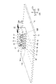
- FIG. 1 is a perspective view showing an optical device according to an embodiment.
- FIG. 2 is a perspective view showing the first optical connector, electrical connector, and host substrate of the host device of the optical device according to the embodiment.
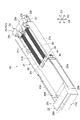
- FIG. 3 is a perspective view showing the internal structure of the light emitting device of the optical device according to the embodiment.
- FIG. 4 is a perspective view showing the light emitting device according to the embodiment.
- FIG. 5 is a front view showing the light emitting device according to the embodiment.
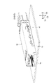
- FIG. 6 is a perspective view showing a state in which the second housing of the light emitting device is inserted into the first housing of the host device according to the embodiment.
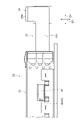
- FIG. 7 is a side view showing a state in which the latch structure of the light emitting device according to the embodiment is engaged with the first housing of the host device;
- FIG. 8 is a perspective view showing a second optical connector according to a modification.
- the optical connector of the optical device has a latch mechanism, there is a concern that the optical connector will become larger due to the latch mechanism. Since there is a concern that the optical connector will become large in this way, there is room for improvement in terms of space saving of the optical device.
- An object of the present disclosure is to provide an optical device that can realize space saving.
- An optical device includes: (1) a host device having a first housing, a first optical connector arranged inside the first housing, and an electrical connector arranged inside the first housing and a second optical connector optically connected to the first optical connector, an electrical plug electrically connected to the electrical connector, and a second optical connector and electrical plug that are inserted into the first housing. and a light emitting device having two housings.
- the second housing has a latch structure that hooks onto the first housing when inserted into the first housing.
- This optical device includes a host device and a light emitting device.
- the host device has a first optical connector, an electrical connector, and a first housing that accommodates the first optical connector and the electrical connector.
- the light emitting device includes a second optical connector, an electrical plug, and a second housing that accommodates the second optical connector and the electrical plug.
- the second housing has a latch structure that hooks onto the first housing. Therefore, the first optical connector and the second optical connector can be configured without the latch structure. Therefore, it is possible to suppress the increase in the size of the optical connector, thereby realizing space saving.
- the second optical connector may have a guide hole
- the first optical connector may have a guide pin to be inserted into the guide hole.
- the guide hole is a guide hole provided in a place other than the MT ferrule (first ferrule, second ferrule).
- the guide pin is a guide pin located outside the MT ferrule.
- the first optical connector may have a first optical fiber and a first ferrule that holds the first optical fiber.
- the second optical connector may have a second optical fiber and a second ferrule holding the second optical fiber.
- the area of the cross section of the opening of the guide hole perpendicular to the direction in which the optical axis of the second optical fiber extends is 0.5% or more and 15% of the area of the cross section of the light emitting device perpendicular to the direction in which the optical axis of the second optical fiber extends. % or less, and may be 5% or more and 60% or less of the area of the end surface of the second ferrule where the second optical fiber is exposed. In this case, the strength of the guide pin inserted into the guide hole can be maintained, and an increase in the size of the light emitting device can be suppressed.
- the first optical connector may have a guide hole.
- the second optical connector may have a guide pin inserted into the guide hole.
- the second optical connector may have an uneven portion formed on the surface of the second optical connector and into which the first optical connector is inserted.
- the surface of the second optical connector is a surface (for example, side surface 59c (see FIG. 8)) other than the abutment surface of the second optical connector with respect to the first optical connector.
- the latch mechanism may further have a mechanism that releases the latch when pulled out.
- FIG. 1 is a perspective view showing an optical device 1 according to an embodiment.
- the optical device 1 includes a host device 10 and a light emitting device 20.
- the optical device 1 is, for example, an opto-electric integrated device that handles both optical and electrical signals.
- the host device 10 has a host substrate 11 extending in both a first direction D1 and a second direction D2, and a first housing 12 mounted on the host substrate 11.
- the light emitting device 20 includes a second housing 21 extending in the first direction D1, a second optical connector 22 housed in the second housing 21, and an electrical plug 23 housed in the second housing 21. have.
- the first housing 12 has an opening 12b directed in the first direction D1.
- the first direction D ⁇ b>1 corresponds to the longitudinal direction of the first housing 12 and the second housing 21
- the second direction D ⁇ b>2 corresponds to the width direction of the first housing 12 and the second housing 21
- the first direction D1, the second direction D2 and the third direction D3 are orthogonal to each other.
- the host device 10 supplies electrical signals to the light emitting device 20 and receives optical signals from the light emitting device 20 .
- the host substrate 11 is a substrate on which electrical components are mounted.
- the host substrate 11 has a main surface 11c on which electrical components are mounted.
- FIG. 2 is a perspective view showing a state in which the first housing 12 is removed from the host device 10.
- FIG. As shown in FIGS. 1 and 2, for example, the host substrate 11 is formed with a plurality of holes 11b in which electronic substrates are mounted.
- the host device 10 has a first optical connector 13 and an electrical connector 14 .
- the first optical connector 13 and the electrical connector 14 are integrated as a block 19, for example.
- the block 19 includes a first portion 19A including the first optical connector 13 and a second portion 19B including the electrical connector 14.
- 19 A of 1st parts and the 2nd part 19B exhibit rectangular parallelepiped shape, for example.
- the area of the second portion 19B is larger than the area of the first portion 19A when viewed from a third direction D3 intersecting (perpendicular to) both the first direction D1 and the second direction D2.
- the third direction D3 corresponds to the out-of-plane direction of the main surface 11c.
- the electrical connector 14 has an opening 14b facing the first direction D1 in the block 19 (second portion 19B).
- An electric plug 23 is inserted into the opening 14b.
- the light emitting device 20 is electrically connected to the host device 10 by inserting the electrical plug 23 into the opening 14b.
- the second optical connector 22 of the light emitting device 20 is optically connected to the first optical connector 13 .
- the first optical connector 13 is provided, for example, at a position further away from the main surface 11c than the electrical connector 14 is.
- the first optical connector 13, the electrical connector 14, and the host substrate 11 are arranged in this order along the third direction D3.
- the first optical connector 13 includes a first optical fiber 15, a first ferrule 16, a guide pin 17, and a ferrule guide pin 18.
- the first optical connector 13 includes two first ferrules 16 arranged along the second direction D2.
- the first ferrule 16 is, for example, an MT ferrule.
- the first optical connector 13 has a plurality of first optical fibers 15 .
- the first ferrule 16 holds a plurality of first optical fibers 15 arranged along the second direction D2. As an example, the number of first optical fibers 15 held by the first ferrule 16 is sixteen.
- the first optical connector 13 has a total of 32 first optical fibers 15 .
- the first optical connector 13 has a through hole 13b penetrating along the first direction D1.
- a first optical fiber 15 and a first ferrule 16 are arranged in the through hole 13b.
- a first ferrule 16 protrudes from the through hole 13b.
- a plurality of first optical fibers 15 extend from the opposite side of the through hole 13 b to the first ferrule 16 .
- the first ferrule 16 has an end face 16b that optically connects to the light emitting device 20. As shown in FIG. Tip surfaces of the plurality of first optical fibers 15 are exposed on the end surface 16b.
- An optical signal is input from the light emitting device 20 to each of the plurality of first optical fibers 15 exposed on the end face 16b.
- the end surface 16b and the tip surface of the first optical fiber 15 are polished so as to be flush with each other.
- the guide pin 17 protrudes in the same direction (first direction D1) as the direction in which the first ferrule 16 protrudes from the through hole 13b.
- Guide pins 17 are provided for positioning the first optical connector 13 with respect to the second optical connector 22 .
- the first optical connector 13 has, for example, two guide pins 17 arranged along the second direction D2.
- the guide pin 17 has, for example, a plate shape extending in both the first direction D1 and the second direction D2.
- the guide pin 17 is provided on the side opposite to the electrical connector 14 when viewed from the first ferrule 16 .
- the pair of guide pins 17 are provided on both end sides of the pair of first ferrules 16 in the second direction D2 when viewed along the third direction D3.
- the first optical connector 13 includes a pair of ferrule guide pins 18 arranged along the second direction D ⁇ b>2 on the end surface 16 b of the first ferrule 16 .
- the ferrule guide pin 18 is provided for positioning the first ferrule 16 and a second ferrule 27 of the second optical connector 22, which will be described later.
- FIG. 3 is a perspective view showing the internal structure of the light emitting device 20.
- the light emitting device 20 has the second housing 21, the second optical connector 22, the electrical plug 23, the light emitting element 24 and the lever 25 described above.
- the second housing 21 includes a lower housing 21A that houses the light emitting element 24, and an upper housing 21B that is a lid that seals the lower housing 21A.
- the direction in which the upper housing 21B is provided with respect to the lower housing 21A may be referred to as the upper side or the upper side
- the direction in which the lower housing 21A is provided with respect to the upper housing 21B may be referred to as the lower side or the lower side.
- the lower housing 21A has a bottom surface 21b, a pair of side surfaces 21c, and an end surface 21d.
- the bottom surface 21b extends in both the first direction D1 and the second direction D2.
- the pair of side surfaces 21c extend in both the first direction D1 and the third direction D3 and are arranged along the second direction D2.
- the end face 21d extends in both the second direction D2 and the third direction D3 at one end in the first direction D1.
- the upper housing 21B has a flat shape extending in both the first direction D1 and the second direction D2.
- the upper housing 21B has an opening 21f through which a portion of the second optical connector 22 is exposed.
- a pair of openings 21f are arranged along the second direction D2.
- the opening 21f has a rectangular shape.
- the area of the second housing 21 when viewed along the first direction D1 is smaller than the area of the opening 12b of the first housing 12, and the shape of the second housing 21 is the opening 12b of the first housing 12. It is a shape that is included in Therefore, the second housing 21 can be inserted into the opening 12b along the first direction D1.
- the second optical connector 22 optically connects to the first optical connector 13 and the electrical plug 23 electrically connects to the electrical connector 14. As shown in FIG.
- the electric plug 23 protrudes from the second housing 21 in the first direction D1.
- the electrical plug 23 has a plate shape.
- the electrical plug 23 has a major surface 23b extending in both the first direction D1 and the second direction D2.
- the electrical plug 23 has a plurality of pads 23c on the principal surface 23b, and the plurality of pads 23c on the principal surface 23b are arranged along the second direction D2.
- the electrical plug 23 can be inserted into the opening 14b of the electrical connector 14. As shown in FIG.
- Each pad 23c of the electrical plug 23 connects to each pad inside the electrical connector 14 when the electrical plug 23 is inserted into the opening 14b. This electrically connects the electrical plug 23 to the electrical connector 14 .
- FIG. 4 is a perspective view showing the light emitting device 20.
- the second optical connector 22 includes a second optical fiber 26 and a second ferrule 27 holding the second optical fiber 26 .
- the second optical connector 22 has a plurality of second optical fibers 26 extending from the second ferrule 27 into the second housing 21 .
- Each of the plurality of second optical fibers 26 is connected to the light emitting element 24 .
- the light emitting element 24 is mounted on a circuit board (not shown) that is electrically connected to the electric plug 23 and receives power through the electric plug 23 .
- the light emitting element 24 emits light by electric power received through the electrical plug 23 , and the light from the light emitting element 24 propagates to the second optical fiber 26 .
- the light emitting device 20 has, for example, two light emitting elements 24, and the two light emitting elements 24 are arranged along the second direction D2.
- the light emitting device 20 has a plurality of second optical fibers 26 .
- the second ferrule 27 holds a plurality of second optical fibers 26 arranged along the second direction D2. As an example, the number of second optical fibers 26 held by the second ferrule 27 is 16, and the second optical connector 22 has a total of 32 second optical fibers 26 .
- the second ferrule 27 is, for example, an MT ferrule.
- the second ferrule 27 has an end surface 27b that connects to the first ferrule 16 described above. Tip surfaces of the plurality of second optical fibers 26 are exposed on the end surface 27b. For example, the end surface 27b and the tip surface of the second optical fiber 26 are polished so as to be flush with each other.
- the second ferrule 27 has a ferrule guide hole 28 into which the ferrule guide pin 18 of the first optical connector 13 is inserted.
- the second ferrule 27 has a pair of ferrule guide holes 28 aligned along the second direction D2. Tip faces of the plurality of second optical fibers 26 are positioned between the pair of ferrule guide holes 28 .
- each second optical fiber 26 is optically connected to each first optical fiber 15 .
- the end surface 27b of the second ferrule 27 may or may not come into contact with the end surface 16b of the first ferrule 16 . That is, the second ferrule 27 may be PC (Physical Contact) connected to the first ferrule 16, or the second optical fiber 26 may be optically connected to the first optical fiber 15 by spatial connection (non-contact). good.
- the second ferrule 27 is positioned with respect to the first ferrule 16 by inserting the ferrule guide pin 18 into the ferrule guide hole 28 .
- the second optical connector 22 has a block 29 that holds the second ferrule 27 .
- the block 29 has a through-hole 29b penetrating along the first direction D1, and the second ferrule 27 is inserted and held in the through-hole 29b.
- the block 29 is provided on the upper side of the second housing 21 (on the side opposite to the bottom surface 21b) when viewed from the electric plug 23.
- Block 29 has a first portion 29A facing electrical plug 23 and a second portion 29B positioned between first portion 29A and upper housing 21B.
- the first portion 29A and the second portion 29B are rectangular, for example.
- the length of the second portion 29B in the second direction D2 is longer than the length of the first portion 29A in the second direction D2.
- the second portion 29B has a convex portion 29c that protrudes upward.
- the second portion 29B has a pair of protrusions 29c arranged along the second direction D2. Each of the pair of protrusions 29c is exposed to each opening 21f.
- the block 29 has a guide hole 30 into which the guide pin 17 is inserted.
- a host device 10 has a guide pin 17 .
- the first optical connector 13 of the host device 10 may have the guide hole 30 and the second optical connector 22 of the light emitting device 20 may have the guide pin 17 . In this case also, the same effect as described above can be obtained.
- the block 29 has an end face 29d where the opening of the through hole 29b and the opening of the guide hole 30 are exposed.
- Two guide holes 30 are arranged along the second direction D2 in the end surface 29d.
- the pair of guide holes 30 are provided on both end sides of the pair of second ferrules 27 in the second direction D2 when viewed along the third direction D3.
- the guide hole 30 is provided between the protrusion 29c and the through hole 29b.
- FIG. 5 is a front view of the second housing 21 and the second optical connector 22 viewed along the first direction D1.
- the opening of the through hole 29b and the opening of the guide hole 30 are both rectangular with long sides extending along the second direction D2 and short sides extending along the third direction D3. present.
- the ratio of the area of the opening of the guide hole 30 to the area of the light emitting device 20 (for example, the portion A of the second housing 21 excluding the lever 25) viewed along the first direction D1 is, for example, 0.5% or more. and 15% or less.
- the ratio of the area of the opening of the guide hole 30 to the area of the end face 27b of the second ferrule 27 is, for example, 5% or more and 60% or less.
- the area of the cross section perpendicular to the direction (first direction D1) in which the optical axis of the second optical fiber 26 extends at the opening of the guide hole 30 is the area of the light emitting device 20 perpendicular to the direction in which the optical axis of the second optical fiber 26 extends. is 0.5% or more and 15% or less of the cross-sectional area of , and 5% or more and 60% or less of the area of the end surface 27b of the second ferrule 27 where the second optical fiber 26 is exposed. Since the area of the opening of the guide hole 30 is 0.5% or more of the area of the portion A and 5% or more of the area of the end face 27b, the strength of the guide pin 17 can be maintained. Further, since the area of the opening of the guide hole 30 is 15% or less of the area of the portion A and 60% or less of the area of the end surface 27b, the size of the light emitting device 20 is suppressed.
- the lever 25 is a part operated when removing the light emitting device 20 from the host device 10 .
- the lever 25 includes a slide portion 25A movably attached to the second housing 21 and a knob portion 25B connected to the slide portion 25A.
- the lever 25 has a pair of slide portions 25A, and each slide portion 25A is provided on each side surface 21c of the second housing 21.
- the slide portion 25A extends from near the center of the second housing 21 in the first direction D1 to the side opposite to the second optical connector 22 .
- the knob portion 25B includes a pair of first extension portions 25b and a second extension portion 25c.
- the pair of first extending portions 25b extends upward from the end of the slide portion 25A opposite to the second optical connector 22 and is arranged along the second direction D2.
- the second extension portion 25c connects the upper ends of the pair of first extension portions 25b.
- the second housing 21 has a latch structure 40 that hooks onto the first housing 12 when inserted into the first housing 12 .
- 6A and 6B are diagrams for explaining the engagement of the latch structure 40 with the first housing 12.
- FIG. As shown in FIGS. 4 and 6, the first housing 12 has a tab 42 with which the second housing 21 engages, and the latch structure 40 spreads the tab 42 outward in the second direction D2.
- a pair of latch structures 40 are provided at the ends of the pair of slide portions 25A (the ends opposite to the knob portion 25B).
- FIG. 7 is a side view showing the first housing 12 of the host device 10.
- FIG. 7 when the second housing 21 is inserted into the first housing 12, the protrusions 41 of the latch structure 40 spread the tabs 42 outward in the second direction D2, so that the protrusions 41 spread the tabs. 42.
- the handle 25B is held by hand and the lever 25 is pulled to the opposite side of the host device 10
- the projection 41 spreads the tab 42 outward in the second direction D2
- the engagement of the latch structure 40 with the tab 42 is released. be. Then, it becomes possible to pull out the light emitting device 20 from the host device 10 .
- the second housing 21 of the light emitting device 20 has a latch structure 40 that hooks onto the first housing 12 of the host device 10 . Therefore, the first optical connector 13 (block 19) and the second optical connector 22 (block 29) can be configured without a latch structure. That is, by providing the second housing 21 with the latch structure 40, the second optical connector 22 accommodated inside the second housing 21 can be configured without the latch structure. Since the first optical connector 13 and the second optical connector 22 can be configured without a latch structure, it is possible to suppress an increase in size of the optical connector and realize space saving.
- the latch structure 40 may further have a mechanism that unlatches when pulled out. That is, as described above, when pulled out, the protrusions 41 of the latch structure 40 may push the tabs 42 outward in the second direction D2 to unlatch the latch structure 40 from the tabs 42 .
- FIG. 8 is a perspective view showing a second optical connector 52 according to a modification. Since a part of the configuration of the second optical connector 52 overlaps with a part of the configuration of the second optical connector 22 described above, the same reference numerals are assigned to the description that overlaps with the second optical connector 22, and the description thereof will be omitted as appropriate. do.
- the second optical connector 52 has an uneven portion 60 into which the first optical connector is inserted instead of the guide hole 30 .
- FIG. 8 shows an example in which the uneven portion 60 is a recess recessed from the surface of the second optical connector 52, and the first optical connector has a protrusion inserted into the recess along the first direction D1.
- the concave-convex portion of the second optical connector 52 may be a convex portion protruding from the surface of the second optical connector 52 .
- the first optical connector has a concave portion inserted along the first direction D1 in the convex portion.
- the second optical connector 52 has a block 59 that holds the second ferrule 27, and the block 59 has an uneven portion 60 formed therein.
- the block 59 has an upper surface 59b extending in both the first direction D1 and the second direction D2, and a pair of side surfaces 59c extending in both the first direction D1 and the third direction D3 and aligned along the second direction D2. and
- the upper surface 59b is, for example, a flat surface.
- the block 59 has, for example, a pair of uneven portions 60 arranged along the second direction D2. Each uneven portion 60 is formed on each side surface 59c.
- the uneven portion 60 is, for example, a pair of inner side surfaces 61 recessed from the side surface 59c and arranged along the third direction D3, and extending in both the first direction D1 and the third direction D3 between the pair of inner side surfaces 61. and a bottom surface 62 .
- the block 59 has an end face 59d in which the opening of the through hole 29b is formed, and a tapered portion 63 is formed between the uneven portion 60 and the end face 59d.
- the tapered portion 63 has a C-shaped opening 63b on the end surface 59d.
- the tapered portion 63 is a portion that widens from the uneven portion 60 toward the end face 59d. Therefore, the area of the opening 63b when viewed along the first direction D1 is larger than the area of the uneven portion 60 when viewed along the first direction D1.
- the tapered portion 63 is defined by a pair of first inclined surfaces 63c and a second inclined surface 63d.
- the pair of first inclined surfaces 63c are inclined from each inner side surface 61 toward the end surface 59d in both the first direction D1 and the third direction D3.
- the second inclined surface 63d extends from the bottom surface 62 toward the end surface 59d and is inclined with respect to both the first direction D1 and the second direction D2. Since the second optical connector 52 is provided with the uneven portion 60 in which the tapered portion 63 is formed, the insertion of the first connector into the second optical connector 52 can be performed smoothly.
- Reference Signs List 1 Optical device 10 Host device 11 Host substrate 11b Hole 11c Main surface 12 First housing 12b Opening 13 First optical connector 13b Through hole 14 Electrical connector 14b Opening 15 First light Fiber 16 First ferrule 16b End face 17 Guide pin 18 Ferrule guide pin 19 Block 19A First part 19B Second part 20 Light emitting device 21 Second housing 21A Lower housing 21B Upper Housing 21b Bottom surface 21c Side surface 21d End surface 21f Openings 22, 52 Second optical connector 23 Electric plug 23b Main surface 23c Pad 24 Light emitting element 25 Lever 25A Slide portion 25B Knob portion 25b First extension portion 25c Second extension portion 26 Second optical fiber 27 Second ferrule 27b End surface 28 Ferrule guide holes 29, 59 Block 29A First portion 29B Second portion 29b Through hole 29c Protruding portion 29d End surface 30 Guide hole 40 Latch structure 41 Projection 42 Tab 59b Upper surface 59c Side surface 59d End surface 60 Uneven portion 61 Inner surface 62 Bottom surface 63 Tapered portion 63b Opening 63c... First inclined surface
Landscapes
- Physics & Mathematics (AREA)
- General Physics & Mathematics (AREA)
- Optics & Photonics (AREA)
- Engineering & Computer Science (AREA)
- Microelectronics & Electronic Packaging (AREA)
- Optical Couplings Of Light Guides (AREA)
- Endoscopes (AREA)
Abstract
Description
本出願は、2021年7月16日の日本出願第2021-118009号に基づく優先権を主張し、前記日本出願に記載された全ての記載内容を援用するものである。
最初に本開示に係る光装置の実施形態について列挙する。一実施形態に係る光装置は、(1)第1筐体、第1筐体の内部に配置される第1光コネクタ、及び、第1筐体の内部に配置される電気コネクタを有するホスト装置と、第1光コネクタに光学的に接続する第2光コネクタ、電気コネクタに電気的に接続する電気プラグ、及び、第2光コネクタ及び電気プラグを収容すると共に第1筐体に挿入される第2筐体を有する発光装置と、を備える。第2筐体は、第1筐体に挿入されたときに第1筐体に引っ掛かるラッチ構造を有する。
実施形態に係る光装置の具体例を以下で図面を参照しながら説明する。本発明は、以下の例示に限定されるものではなく、請求の範囲に示され、請求の範囲と均等の範囲における全ての変更が含まれることが意図される。図面の説明において同一又は相当する要素には同一の符号を付し、重複する説明を適宜省略する。図面は、理解の容易化のため、一部を簡略化又は誇張して描いている場合があり、寸法比率等は図面に記載のものに限定されない。
10…ホスト装置
11…ホスト基板
11b…穴
11c…主面
12…第1筐体
12b…開口
13…第1光コネクタ
13b…貫通孔
14…電気コネクタ
14b…開口
15…第1光ファイバ
16…第1フェルール
16b…端面
17…ガイドピン
18…フェルール用ガイドピン
19…ブロック
19A…第1部分
19B…第2部分
20…発光装置
21…第2筐体
21A…下筐体
21B…上筐体
21b…底面
21c…側面
21d…端面
21f…開口
22,52…第2光コネクタ
23…電気プラグ
23b…主面
23c…パッド
24…発光素子
25…レバー
25A…スライド部
25B…摘まみ部
25b…第1延在部
25c…第2延在部
26…第2光ファイバ
27…第2フェルール
27b…端面
28…フェルール用ガイド穴
29,59…ブロック
29A…第1部分
29B…第2部分
29b…貫通孔
29c…凸部
29d…端面
30…ガイド穴
40…ラッチ構造
41…突起
42…タブ
59b…上面
59c…側面
59d…端面
60…凹凸部
61…内側面
62…底面
63…テーパ部
63b…開口
63c…第1傾斜面
63d…第2傾斜面
D1…第1方向
D2…第2方向
D3…第3方向
Claims (6)
- 第1筐体、前記第1筐体の内部に配置される第1光コネクタ、及び、前記第1筐体の内部に配置される電気コネクタを有するホスト装置と、
前記第1光コネクタに光学的に接続する第2光コネクタ、前記電気コネクタに電気的に接続する電気プラグ、及び、前記第2光コネクタ及び前記電気プラグを収容すると共に前記第1筐体に挿入される第2筐体を有する発光装置と、を備え、
前記第2筐体は、前記第1筐体に挿入されたときに前記第1筐体に引っ掛かるラッチ構造を有する、
光装置。 - 前記第2光コネクタは、ガイド穴を有し、
前記第1光コネクタは、前記ガイド穴に挿入されるガイドピンを有する、
請求項1に記載の光装置。 - 前記第1光コネクタは、第1光ファイバと、前記第1光ファイバを保持する第1フェルールとを有し、
前記第2光コネクタは、第2光ファイバと、前記第2光ファイバを保持する第2フェルールとを有し、
前記ガイド穴の開口の前記第2光ファイバの光軸が延びる方向に直交する断面の面積は、前記第2光ファイバの光軸が延びる方向に直交する前記発光装置の断面の面積の0.5%以上且つ15%以下であり、前記第2光ファイバが露出する前記第2フェルールの端面の面積の5%以上且つ60%以下である、
請求項2に記載の光装置。 - 前記第1光コネクタは、ガイド穴を有し、
前記第2光コネクタは、前記ガイド穴に挿入されるガイドピンを有する、
請求項1に記載の光装置。 - 前記第2光コネクタは、前記第2光コネクタの表面に形成されており前記第1光コネクタが挿入される凹凸部を有する、
請求項1に記載の光装置。 - 前記ラッチ構造は、更に、引き抜かれるときにラッチが外れる機構を有する、
請求項1~5のいずれか一項に記載の光装置。
Priority Applications (3)
| Application Number | Priority Date | Filing Date | Title |
|---|---|---|---|
| US18/007,958 US12468101B2 (en) | 2021-07-16 | 2022-05-23 | Optical device |
| JP2023535159A JP7816356B2 (ja) | 2021-07-16 | 2022-05-23 | 光装置 |
| CN202280046791.4A CN117581137A (zh) | 2021-07-16 | 2022-05-23 | 光装置 |
Applications Claiming Priority (2)
| Application Number | Priority Date | Filing Date | Title |
|---|---|---|---|
| JP2021-118009 | 2021-07-16 | ||
| JP2021118009 | 2021-07-16 |
Publications (1)
| Publication Number | Publication Date |
|---|---|
| WO2023286455A1 true WO2023286455A1 (ja) | 2023-01-19 |
Family
ID=84919921
Family Applications (1)
| Application Number | Title | Priority Date | Filing Date |
|---|---|---|---|
| PCT/JP2022/021141 Ceased WO2023286455A1 (ja) | 2021-07-16 | 2022-05-23 | 光装置 |
Country Status (5)
| Country | Link |
|---|---|
| US (1) | US12468101B2 (ja) |
| JP (1) | JP7816356B2 (ja) |
| CN (1) | CN117581137A (ja) |
| TW (1) | TW202309577A (ja) |
| WO (1) | WO2023286455A1 (ja) |
Cited By (2)
| Publication number | Priority date | Publication date | Assignee | Title |
|---|---|---|---|---|
| US11934020B2 (en) | 2021-02-12 | 2024-03-19 | Senko Advanced Components, Inc. | Optoelectronic connections to printed circuit boards |
| WO2025243976A1 (ja) * | 2024-05-21 | 2025-11-27 | 株式会社白山 | レセプタクル、プラグ、光コネクタおよび光電気回路基板の製造方法 |
Citations (6)
| Publication number | Priority date | Publication date | Assignee | Title |
|---|---|---|---|---|
| JPH04230978A (ja) * | 1990-04-23 | 1992-08-19 | E I Du Pont De Nemours & Co | 電子・光信号変換装置 |
| JPH08265180A (ja) * | 1995-01-13 | 1996-10-11 | Methode Electronics Inc | トランシーバモジュール及びレセプタクルアセンブリ |
| JP2012220541A (ja) * | 2011-04-04 | 2012-11-12 | Fujitsu Component Ltd | コネクタ |
| US20140254993A1 (en) * | 2013-03-05 | 2014-09-11 | Finisar Corporation | Latch mechanism for communication module |
| WO2015046488A1 (ja) * | 2013-09-30 | 2015-04-02 | 京セラ株式会社 | 光コネクタ、光伝送モジュールおよび光コネクタ用プラグ |
| JP2015153609A (ja) * | 2014-02-14 | 2015-08-24 | 日本航空電子工業株式会社 | 光電複合コネクタ及び携帯型電子機器 |
Family Cites Families (11)
| Publication number | Priority date | Publication date | Assignee | Title |
|---|---|---|---|---|
| US5546281A (en) | 1995-01-13 | 1996-08-13 | Methode Electronics, Inc. | Removable optoelectronic transceiver module with potting box |
| US6305848B1 (en) | 2000-06-19 | 2001-10-23 | Corona Optical Systems, Inc. | High density optoelectronic transceiver module |
| US6676302B2 (en) * | 2001-09-17 | 2004-01-13 | Stratos Lightwave, Inc. | Method of constructing a fiber optics communications module |
| JP4632289B2 (ja) * | 2002-03-06 | 2011-02-16 | タイコ・エレクトロニクス・コーポレイション | プラグ接続可能な電子モジュール及びヒートシンク付きリセプタクル |
| US7934959B2 (en) * | 2009-10-06 | 2011-05-03 | Mellanox Technologies Ltd. | Adapter for pluggable module |
| JP2013200394A (ja) * | 2012-03-23 | 2013-10-03 | Yamaichi Electronics Co Ltd | リセプタクルアッセンブリー、および、トランシーバモジュールアッセンブリー |
| CN105637715A (zh) | 2013-09-09 | 2016-06-01 | 日本航空电子工业株式会社 | 光电复合连接器及便携式电子设备 |
| US10079451B2 (en) * | 2016-11-14 | 2018-09-18 | Te Connectivity Corporation | Pull tab device for a latch of a pluggable module |
| US11300738B2 (en) * | 2018-11-08 | 2022-04-12 | Hewlett Packard Enterprise Development Lp | Connector assembly including a housing-attachable optical connector |
| US11314026B2 (en) * | 2018-11-19 | 2022-04-26 | Hewlett Packard Enterprise Development Lp | Connector assembly including an edge-attachable optical connector housing and optical connector |
| JP2021043422A (ja) * | 2019-09-13 | 2021-03-18 | 小池 康博 | 一括成型マルチ光伝送シートアセンブリ、接続構造体、光モジュール、アクティブ光ケーブルおよびその製造方法 |
-
2022
- 2022-05-23 JP JP2023535159A patent/JP7816356B2/ja active Active
- 2022-05-23 US US18/007,958 patent/US12468101B2/en active Active
- 2022-05-23 CN CN202280046791.4A patent/CN117581137A/zh active Pending
- 2022-05-23 WO PCT/JP2022/021141 patent/WO2023286455A1/ja not_active Ceased
- 2022-07-01 TW TW111124765A patent/TW202309577A/zh unknown
Patent Citations (6)
| Publication number | Priority date | Publication date | Assignee | Title |
|---|---|---|---|---|
| JPH04230978A (ja) * | 1990-04-23 | 1992-08-19 | E I Du Pont De Nemours & Co | 電子・光信号変換装置 |
| JPH08265180A (ja) * | 1995-01-13 | 1996-10-11 | Methode Electronics Inc | トランシーバモジュール及びレセプタクルアセンブリ |
| JP2012220541A (ja) * | 2011-04-04 | 2012-11-12 | Fujitsu Component Ltd | コネクタ |
| US20140254993A1 (en) * | 2013-03-05 | 2014-09-11 | Finisar Corporation | Latch mechanism for communication module |
| WO2015046488A1 (ja) * | 2013-09-30 | 2015-04-02 | 京セラ株式会社 | 光コネクタ、光伝送モジュールおよび光コネクタ用プラグ |
| JP2015153609A (ja) * | 2014-02-14 | 2015-08-24 | 日本航空電子工業株式会社 | 光電複合コネクタ及び携帯型電子機器 |
Cited By (3)
| Publication number | Priority date | Publication date | Assignee | Title |
|---|---|---|---|---|
| US11934020B2 (en) | 2021-02-12 | 2024-03-19 | Senko Advanced Components, Inc. | Optoelectronic connections to printed circuit boards |
| US12411298B2 (en) | 2021-02-12 | 2025-09-09 | Senko Advanced Components, Inc. | Optoelectronic connections to printed circuit boards |
| WO2025243976A1 (ja) * | 2024-05-21 | 2025-11-27 | 株式会社白山 | レセプタクル、プラグ、光コネクタおよび光電気回路基板の製造方法 |
Also Published As
| Publication number | Publication date |
|---|---|
| JPWO2023286455A1 (ja) | 2023-01-19 |
| TW202309577A (zh) | 2023-03-01 |
| US20240231020A1 (en) | 2024-07-11 |
| US12468101B2 (en) | 2025-11-11 |
| CN117581137A (zh) | 2024-02-20 |
| JP7816356B2 (ja) | 2026-02-18 |
Similar Documents
| Publication | Publication Date | Title |
|---|---|---|
| JP5692005B2 (ja) | 光モジュール及び信号伝送媒体 | |
| US20070230874A1 (en) | Fiber adapter and shutter member thereof | |
| TWI487217B (zh) | 光電子模組連接器系統,使用此系統之方法及光電子模組連接器系統套組 | |
| JP2002048953A (ja) | 光ファイバシステム | |
| US20110123156A1 (en) | Optical adapter | |
| CA2836675A1 (en) | Optical connector | |
| JP2017134401A (ja) | 光トランシーバ | |
| WO2023286455A1 (ja) | 光装置 | |
| JP4323433B2 (ja) | 光ファイバコネクタモジュール | |
| US20120128302A1 (en) | Optical connector device and mating optical connector device | |
| US9581773B2 (en) | Cage, communication device, communication module and connecting method | |
| US7056156B1 (en) | Vertically offset EMI projections | |
| US20130077919A1 (en) | Optical-electrical connector having a magnetic member | |
| TWI437299B (zh) | 能腹對腹佈局且無框架的可插拔光電裝置 | |
| JP4297279B2 (ja) | 光コネクタ | |
| JPWO2019146223A1 (ja) | 光接続構造、光コネクタ部品、及びハウジング | |
| US11137554B2 (en) | Optical connection structure | |
| WO2020017255A1 (ja) | 光コネクタ、及び、光コネクタ用交換部品ユニット | |
| JP2004145005A (ja) | 光コネクタ装置 | |
| JP3135572U (ja) | 内蔵式防塵装置付きコネクタ | |
| JP2020013009A (ja) | 光コネクタ、及び、光コネクタ用交換部品ユニット | |
| JP2025150550A (ja) | フェルールホルダ、光接続構造、光モジュール | |
| JP2018205348A (ja) | 光コネクタ | |
| JP6536952B2 (ja) | 通信モジュール及び通信モジュール用コネクタ | |
| CN106252931B (zh) | 通信模块以及通信模块用连接器 |
Legal Events
| Date | Code | Title | Description |
|---|---|---|---|
| WWE | Wipo information: entry into national phase |
Ref document number: 18007958 Country of ref document: US |
|
| 121 | Ep: the epo has been informed by wipo that ep was designated in this application |
Ref document number: 22841802 Country of ref document: EP Kind code of ref document: A1 |
|
| WWE | Wipo information: entry into national phase |
Ref document number: 2023535159 Country of ref document: JP |
|
| WWE | Wipo information: entry into national phase |
Ref document number: 202280046791.4 Country of ref document: CN |
|
| NENP | Non-entry into the national phase |
Ref country code: DE |
|
| 122 | Ep: pct application non-entry in european phase |
Ref document number: 22841802 Country of ref document: EP Kind code of ref document: A1 |
|
| WWG | Wipo information: grant in national office |
Ref document number: 18007958 Country of ref document: US |