WO2023286235A1 - 炭化珪素半導体装置および電力変換装置 - Google Patents
炭化珪素半導体装置および電力変換装置 Download PDFInfo
- Publication number
- WO2023286235A1 WO2023286235A1 PCT/JP2021/026592 JP2021026592W WO2023286235A1 WO 2023286235 A1 WO2023286235 A1 WO 2023286235A1 JP 2021026592 W JP2021026592 W JP 2021026592W WO 2023286235 A1 WO2023286235 A1 WO 2023286235A1
- Authority
- WO
- WIPO (PCT)
- Prior art keywords
- region
- regions
- silicon carbide
- pillar
- mosfet
- Prior art date
- Legal status (The legal status is an assumption and is not a legal conclusion. Google has not performed a legal analysis and makes no representation as to the accuracy of the status listed.)
- Ceased
Links
Images












Classifications
-
- H—ELECTRICITY
- H10—SEMICONDUCTOR DEVICES; ELECTRIC SOLID-STATE DEVICES NOT OTHERWISE PROVIDED FOR
- H10D—INORGANIC ELECTRIC SEMICONDUCTOR DEVICES
- H10D12/00—Bipolar devices controlled by the field effect, e.g. insulated-gate bipolar transistors [IGBT]
-
- H—ELECTRICITY
- H10—SEMICONDUCTOR DEVICES; ELECTRIC SOLID-STATE DEVICES NOT OTHERWISE PROVIDED FOR
- H10D—INORGANIC ELECTRIC SEMICONDUCTOR DEVICES
- H10D62/00—Semiconductor bodies, or regions thereof, of devices having potential barriers
- H10D62/10—Shapes, relative sizes or dispositions of the regions of the semiconductor bodies; Shapes of the semiconductor bodies
- H10D62/102—Constructional design considerations for preventing surface leakage or controlling electric field concentration
- H10D62/103—Constructional design considerations for preventing surface leakage or controlling electric field concentration for increasing or controlling the breakdown voltage of reverse-biased devices
- H10D62/105—Constructional design considerations for preventing surface leakage or controlling electric field concentration for increasing or controlling the breakdown voltage of reverse-biased devices by having particular doping profiles, shapes or arrangements of PN junctions; by having supplementary regions, e.g. junction termination extension [JTE]
- H10D62/106—Constructional design considerations for preventing surface leakage or controlling electric field concentration for increasing or controlling the breakdown voltage of reverse-biased devices by having particular doping profiles, shapes or arrangements of PN junctions; by having supplementary regions, e.g. junction termination extension [JTE] having supplementary regions doped oppositely to or in rectifying contact with regions of the semiconductor bodies, e.g. guard rings with PN or Schottky junctions
-
- H—ELECTRICITY
- H10—SEMICONDUCTOR DEVICES; ELECTRIC SOLID-STATE DEVICES NOT OTHERWISE PROVIDED FOR
- H10D—INORGANIC ELECTRIC SEMICONDUCTOR DEVICES
- H10D30/00—Field-effect transistors [FET]
- H10D30/60—Insulated-gate field-effect transistors [IGFET]
-
- H—ELECTRICITY
- H10—SEMICONDUCTOR DEVICES; ELECTRIC SOLID-STATE DEVICES NOT OTHERWISE PROVIDED FOR
- H10D—INORGANIC ELECTRIC SEMICONDUCTOR DEVICES
- H10D30/00—Field-effect transistors [FET]
- H10D30/60—Insulated-gate field-effect transistors [IGFET]
- H10D30/64—Double-diffused metal-oxide semiconductor [DMOS] FETs
- H10D30/66—Vertical DMOS [VDMOS] FETs
- H10D30/668—Vertical DMOS [VDMOS] FETs having trench gate electrodes, e.g. UMOS transistors
-
- H—ELECTRICITY
- H10—SEMICONDUCTOR DEVICES; ELECTRIC SOLID-STATE DEVICES NOT OTHERWISE PROVIDED FOR
- H10D—INORGANIC ELECTRIC SEMICONDUCTOR DEVICES
- H10D62/00—Semiconductor bodies, or regions thereof, of devices having potential barriers
- H10D62/01—Manufacture or treatment
- H10D62/051—Forming charge compensation regions, e.g. superjunctions
- H10D62/058—Forming charge compensation regions, e.g. superjunctions by using trenches, e.g. implanting into sidewalls of trenches or refilling trenches
-
- H—ELECTRICITY
- H10—SEMICONDUCTOR DEVICES; ELECTRIC SOLID-STATE DEVICES NOT OTHERWISE PROVIDED FOR
- H10D—INORGANIC ELECTRIC SEMICONDUCTOR DEVICES
- H10D62/00—Semiconductor bodies, or regions thereof, of devices having potential barriers
- H10D62/10—Shapes, relative sizes or dispositions of the regions of the semiconductor bodies; Shapes of the semiconductor bodies
- H10D62/102—Constructional design considerations for preventing surface leakage or controlling electric field concentration
- H10D62/103—Constructional design considerations for preventing surface leakage or controlling electric field concentration for increasing or controlling the breakdown voltage of reverse-biased devices
- H10D62/105—Constructional design considerations for preventing surface leakage or controlling electric field concentration for increasing or controlling the breakdown voltage of reverse-biased devices by having particular doping profiles, shapes or arrangements of PN junctions; by having supplementary regions, e.g. junction termination extension [JTE]
- H10D62/109—Reduced surface field [RESURF] PN junction structures
- H10D62/111—Multiple RESURF structures, e.g. double RESURF or 3D-RESURF structures
-
- H—ELECTRICITY
- H10—SEMICONDUCTOR DEVICES; ELECTRIC SOLID-STATE DEVICES NOT OTHERWISE PROVIDED FOR
- H10D—INORGANIC ELECTRIC SEMICONDUCTOR DEVICES
- H10D62/00—Semiconductor bodies, or regions thereof, of devices having potential barriers
- H10D62/80—Semiconductor bodies, or regions thereof, of devices having potential barriers characterised by the materials
- H10D62/83—Semiconductor bodies, or regions thereof, of devices having potential barriers characterised by the materials being Group IV materials, e.g. B-doped Si or undoped Ge
- H10D62/832—Semiconductor bodies, or regions thereof, of devices having potential barriers characterised by the materials being Group IV materials, e.g. B-doped Si or undoped Ge being Group IV materials comprising two or more elements, e.g. SiGe
- H10D62/8325—Silicon carbide
Definitions
- the present disclosure relates to silicon carbide semiconductor devices.
- Transistor insulated gate bipolar transistor
- the depletion layer extends in the drift layer and functions as a breakdown voltage layer. If the thickness of the drift layer is small or the impurity concentration of the drift layer is high, only a thin depletion layer is formed, and the breakdown voltage of the device is lowered.
- the ON resistance which is the resistance of the drift layer
- the drift resistance is one of the main resistance components of the MOSFET because it is higher than the resistance of the semiconductor substrate. Therefore, the on-resistance can be substantially lowered by lowering the drift resistance.
- a typical method for lowering the on-resistance is to reduce the thickness of the drift layer or to increase the impurity concentration of the drift layer. For the above reasons, there is a trade-off between high breakdown voltage and low on-resistance.
- a superjunction structure (hereinafter also referred to as an SJ structure) has been proposed as a structure that solves the trade-off between breakdown voltage and on-resistance.
- SJ structure in the drift layer, p-type pillars and n-type pillars are alternately arranged along the direction orthogonal to the direction of current flow.
- the depletion layer in addition to the depletion layer spreading from the pn junction surface or metal junction surface existing near the surface of the semiconductor element, the depletion layer also spreads from the pn junction surface between the p-type pillar and the n-type pillar. That is, a depletion layer is formed in the drift layer to the same depth as the p-type pillar or the n-type pillar.
- the conductivity type of the drift layer is n-type
- the impurity concentration of the n-type pillar is increased to reduce the drift resistance
- the impurity concentration balance between the n-type pillar and the p-type pillar is maintained.
- a high withstand voltage can be maintained by completely depleting the insides of the n-type pillar and the p-type pillar. Therefore, the SJ structure is expected to dramatically improve the trade-off between the breakdown voltage and the on-resistance of the semiconductor device.
- the multi-epitaxial method is a method in which an epitaxial growth process and an ion implantation process are alternately repeated.
- the embedded epitaxial method is a method of forming a trench in an epitaxial layer and then forming an epitaxial layer to fill the trench. In either method, there is a limit to reducing the spacing of the pillar structures. In particular, in the case of a semiconductor device using silicon carbide (SiC), which is rapidly spreading at present as a wide bandgap material, it is difficult to reduce the interval of the pillar structure as described below.
- SiC generally has a very small thermal diffusion coefficient of impurities.
- Al and B which are p-type impurities, also have very small thermal diffusion coefficients in SiC. Therefore, in order to form the p-type region by the multi-epitaxial method, it is necessary to form a uniform profile by performing high-energy ion implantation multiple times. Therefore, in the multi-epitaxial method, it is necessary to form a thick resist film for ion implantation and separately create regions into which ions are implanted and regions into which ions are not implanted.
- the embedded epitaxial method also has the same problem. Compared to silicon (Si), which is mainly used in power devices, SiC has a strong bonding force between atoms, so it is difficult to etch by reactive ion etching (RIE) or the like. Therefore, SiC has a smaller selectivity with respect to an etching mask than Si, and the aspect ratio of trenches that can be formed by etching is more limited. Therefore, in SiC, even if the embedded epitaxial method is used, there is a limit to the practical width of the p-type pillar. As described above, in SiC, the pillar spacing of the SJ structure tends to be wider than in Si.
- RIE reactive ion etching
- SiC has the problem that the channel resistance of the MOSFET becomes very high.
- the channel mobility of an n-type Si-MOSFET is about several hundred cm 2 /Vs, while that of an n-type SiC-MOSFET is only about several tens of cm 2 /Vs.
- SiC has a problem that the mobility of holes is very low.
- the hole mobility is about 500 cm 2 /Vs, which is about one third of the electron mobility of about 1500 cm 2 /Vs.
- the hole mobility is about 100 cm 2 /Vs, which is about 1/10 of the electron mobility of about 1100 cm 2 /Vs.
- the high dielectric breakdown electric field which is a feature of SiC, produces the merit of lowering the resistance of the drift layer, but causes the problem of an increase in the electric field in the gate insulating film provided in contact with SiC.
- the SiC-MOSFET has a problem that the lifetime of the gate insulating film is shortened due to the increase in the electric field in the JFET region, which was not taken into consideration in the SiC-MOSFET with a small breakdown electric field. Therefore, in SiC-MOSFETs, the JFET region must be formed narrower than in Si-MOSFETs. As the JFET region becomes narrower, the resistance of the JFET region (JFET resistance) increases, which becomes an obstacle to reducing the on-resistance in the same way as the increase in channel resistance, particularly in low-voltage elements.
- the repetition period of the MOSFET is made smaller than the repetition period of the p-type pillar. can be considered. As a result, the channel width density of SiC is increased, and the resistance is reduced.
- the repetition period of the MOSFET is set to be smaller than the repetition period of the p-type pillar, if the MOSFET and the p-pillar repeat in the same direction, the repetition period of the MOSFET is an integer fraction of the repetition period of the p-type pillar. Limited to 1.
- variations in breakdown voltage occur due to misalignment between the MOSFET and the SJ region. This is because the electric field applied to the pn junction varies greatly depending on where the JFET region of the MOSFET is positioned between the p-type pillars.
- the present disclosure has been made to solve the above problems, and in a silicon carbide semiconductor device having an SJ structure and an insulated gate structure, a low-resistance contact is realized in a pillar region and variations in breakdown voltage are suppressed. , to reduce channel resistance and JFET resistance.
- a silicon carbide semiconductor device of the present disclosure includes an n-type silicon carbide substrate having a first main surface and a second main surface facing each other, and an SJ region made of silicon carbide provided on the first main surface of the silicon carbide substrate. , and a MOSFET region provided on the upper surface of the SJ region.
- the SJ regions are a plurality of n-type first pillar regions extending in a first direction parallel to the first main surface and alternately arranged in a second direction parallel to the first main surface and perpendicular to the first direction. and p-type second pillar regions.
- the MOSFET region extends in the second direction, is arranged in the first direction with a second repetition period shorter than the first repetition period, which is the repetition period of the second pillar region, and is connected to the second pillar region, p-type a plurality of BPW regions made of silicon carbide, a plurality of gate electrodes provided in respective trenches provided in the second direction over the respective BPW regions with gate insulating films interposed therebetween, and between two adjacent BPW regions, and a plurality of JFET regions made of n-type silicon carbide extending in the second direction between two adjacent trenches, and p-type silicon carbide provided on and in contact with each JFET region.
- the silicon carbide semiconductor device includes an upper electrode provided on each body contact region and a lower electrode provided on the second main surface of the silicon carbide substrate.
- FIG. 1 is a schematic plan view of an SJ-SiC-MOSFET of Embodiment 1 or Embodiment 2;
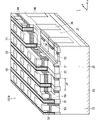
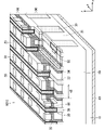
- FIG. 2 is a perspective view of a unit cell of the SJ-SiC-MOSFET of Embodiment 1;
- FIG. 2 is a perspective view of a unit cell of the SJ-SiC-MOSFET of Embodiment 1;
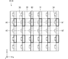
- FIG. 2 is an xy plan view of a boundary portion between an SJ region and a MOSFET region of SJ-SiC-MOSFET 101 of Embodiment 1.
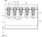
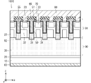
- FIG. FIG. 5 is a cross-sectional view of SJ-SiC-MOSFET 101 of Embodiment 1 taken along line A1-A1′ in FIG. 4;
- FIG. 5 is a cross-sectional view of the SJ-SiC-MOSFET 101 of the first embodiment taken along the line A2-A2′ in FIG. 4;
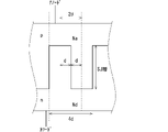
- FIG. 10 is a diagram showing a pn diode structure used for a trial calculation example of optimum design of the SJ region;
- FIG. 4 is a diagram showing the relationship between pillar pitch, on-resistance, and impurity concentration in an optimized SJ region; 7 shows TCAD simulation results of the electric field distribution on top of the pn diode structure of FIG. 6;
- FIG. FIG. 4 is a diagram showing the relationship between the average current density and sheet resistance in the conduction path of holes from the intersection region to the source electrode, and the impurity concentration of the first pillar region;
- FIG. 4 is a diagram showing acceptor impurity concentration dependence of hole mobility and ionization rate in a p-type region;
- FIG. 4 is a diagram showing acceptor impurity concentration dependence of the resistivity of a p-type region;
- FIG. 4 is a diagram showing the relationship between the impurity concentration of the connection region and the area occupation ratio in the xy plane;
- FIG. 4 shows a diode structure used for TCAD calculations;
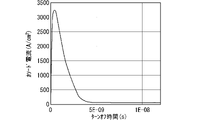
- FIG. 4 is a diagram showing a time waveform of a current flowing through a cathode;
- FIG. 10 is a diagram showing a time waveform of a voltage difference between immediately above and below the mobility-reduced region;
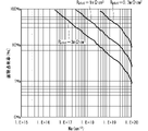
- FIG. 10 is a diagram showing the results of trial calculations of the relationship between the impurity concentration of the connection region and the area occupation ratio in the xy plane when the resistivity of the connection region is 1 m ⁇ cm 2 and 0.3 m ⁇ cm 2 ;
- FIG. 10 is a perspective view of a unit cell of an SJ-SiC-MOSFET of a first modified example of the first embodiment;
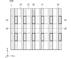
- FIG. 10 is a plan view in the xy plane passing through the intersection region of the SJ-SiC-MOSFET of the first modification of the first embodiment;
- FIG. 20 is a cross-sectional view of the SJ-SiC-MOSFET of the first modification of the first embodiment taken along the line A1-A1′ in FIG. 19;
- FIG. 20 is a cross-sectional view of the SJ-SiC-MOSFET of the first modification of the first embodiment taken along the line A2-A2′ in FIG. 19;
- 10 is a perspective view of a unit cell of an SJ-SiC-MOSFET of a second modification of the first embodiment;
- FIG. FIG. 10 is a plan view in the xy plane passing through the intersection region of the SJ-SiC-MOSFET of the second modification of the first embodiment;
- FIG. 24 is a cross-sectional view of the SJ-SiC-MOSFET of the second modification of the first embodiment taken along the line A1-A1′ in FIG. 23;
- FIG. 24 is a cross-sectional view of the SJ-SiC-MOSFET of the second modification of the first embodiment taken along the line A2-A2′ in FIG. 23;
- 10 is a perspective view of a unit cell of an SJ-SiC-MOSFET of a third modified example of the first embodiment;
- FIG. FIG. 10 is a plan view in the xy plane passing through the intersection region of the SJ-SiC-MOSFET of the third modification of the first embodiment;
- FIG. 28 is a cross-sectional view of the SJ-SiC-MOSFET of the third modification of the first embodiment taken along the line A1-A1′ in FIG. 27;
- FIG. 28 is a cross-sectional view of the SJ-SiC-MOSFET of the third modification of the first embodiment taken along the line A2-A2′ in FIG. 27; 10 is a cross-sectional view along the xz plane passing through the first pillar region of the SJ-SiC-MOSFET of the fourth modification of the first embodiment; FIG. 10 is a cross-sectional view along the xz plane passing through the second pillar region of the SJ-SiC-MOSFET of the fourth modification of the first embodiment; FIG. FIG. 10 is a perspective view of a unit cell of the SJ-SiC-MOSFET of Embodiment 2; FIG.
- FIG. 10 is a perspective view of a unit cell of an SJ-SiC-MOSFET of a first modified example of the second embodiment
- FIG. 11 is a perspective view of a unit cell of an SJ-SiC-MOSFET of a second modified example of the second embodiment
- FIG. 11 is a perspective view of a unit cell of an SJ-SiC-MOSFET of a third modified example of the second embodiment
- FIG. 10 is a configuration diagram of a power conversion system according to Embodiment 3;
- a silicon carbide (SiC) semiconductor device is used as an example of a semiconductor device, and an n-channel silicon carbide MOSFET having a first conductivity type of n type and a second conductivity type of p type.
- SiC silicon carbide
- MOSFET having a first conductivity type of n type and a second conductivity type of p type.
- the description about the level of the potential is for the case where the first conductivity type is n-type and the second conductivity type is p-type. , the description of the high and low potentials is also reversed.
- the region other than the active region where the unit cells are arranged periodically is referred to as the peripheral region in the present application.
- Embodiment 1 > ⁇ A-1. Configuration> First, the configuration of the silicon carbide semiconductor device according to the first embodiment will be described.
- FIG. 1 shows a silicon carbide MOSFET (hereinafter referred to as SJ-SiC-MOSFET) 101 having an SJ structure which is the silicon carbide semiconductor device of the first embodiment or SJ-SiC which is the silicon carbide semiconductor device of the second embodiment.
- SJ-SiC-MOSFET silicon carbide MOSFET
- FIG. 1 It is a schematic plan view of the MOSFET 102 viewed from above.
- a gate pad 81 is formed on part of the upper surfaces of the SJ-SiC-MOSFETs 101 and 102, and a source electrode 80 is formed adjacent thereto.
- a gate wiring 82 is formed extending from gate pad 81 .
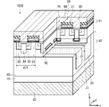
- FIG. 2 is a perspective view of a unit cell of the SJ-SiC-MOSFET 101.
- FIG. 2 the structure above the MOSFET region 91 is omitted in order to visualize the structure of the unit cell.
- the unit cell of SJ-SiC-MOSFET 101 shown in FIG. 2 is periodically repeated under the source electrode 80 of FIG.
- the z-axis direction in FIG. 2 is the surface direction of the chip forming the SJ-SiC-MOSFET 101 .
- the x-axis direction and the y-axis direction in FIG. are not necessarily defined uniquely and have a certain degree of arbitrariness.
- the x-axis and the y-axis should be horizontal to the surface direction of the chip and perpendicular to the z-axis, and form an angle of at least a certain value, for example, 10° or more.
- FIG. 2 shows only the region inside the semiconductor layer made of SiC and the trench gate location.
- FIG. 2 shows the SJ-SiC-MOSFET 101 cut at various cross sections.
- the SJ-SiC-MOSFET 101 includes an n-type silicon carbide substrate 10, an n-type drift layer 20, an SJ region 90 and a MOSFET region 91.
- the upper and lower surfaces of silicon carbide substrate 10 in FIG. 2 are also referred to as a first main surface and a second main surface, respectively.
- Drift layer 20 is formed on silicon carbide substrate 10 .
- SJ region 90 is formed on drift layer 20 .
- MOSFET region 91 is formed on SJ region 90 .
- SJ region 90 is not in contact with silicon carbide substrate 10 in FIG. 2, it may be in contact with silicon carbide substrate 10 as shown in FIG. That is, SJ region 90 may be formed on silicon carbide substrate 10 with drift layer 20 interposed therebetween, or may be formed directly on silicon carbide substrate 10 .
- the SJ region 90 includes a plurality of n-type first pillar regions 21 and a plurality of p-type second pillar regions 30 .
- Each first pillar region 21 and each second pillar region 30 extend in the x-axis direction and are alternately arranged in stripes in the y-axis direction at a repetition period d1. That is, each first pillar region 21 and each second pillar region 30 extend in the x-axis direction, which is the first direction parallel to the first main surface of silicon carbide substrate 10, and parallel to the first main surface and to the x-axis. are alternately arranged in the y-axis direction, which is the second direction perpendicular to the .
- the repetition period d1 is also called a first repetition period.
- a small portion of second pillar region 30 may extend into MOSFET region 91 .
- the impurity concentrations of the first pillar region 21 and the second pillar region 30 may fluctuate due to variations in the process, etc., it is desirable that they be designed so as to generally achieve charge balance.
- Charge balance means that the sum of space charge densities when the regions at the same depth of the first pillar region 21 and the second pillar region 30 are completely depleted is almost zero due to cancellation of positive and negative charges.
- the product of the width of the first pillar region 21 and the impurity concentration of the first pillar region 21 is substantially equal to the product of the width of the second pillar region 30 and the impurity concentration of the second pillar region 30 .
- SJ region 90 may be designed.
- the MOSFET region 91 includes an n-type JFET region 22, a p-type body region 32, a source region 23 which is an n-type impurity region, a p-type body contact region 33, a gate insulating film 50, a gate electrode 60, and a p-type impurity region.
- a BPW region 31 and a p-type connection region 34 are provided.
- a JFET region 22 is formed over the SJ region 90 .
- Body region 32 is formed over JFET region 22 .
- Source region 23 is formed over body region 32 .
- Body contact region 33 is formed to reach body region 32 from the upper surface of source region 23 through source region 23 .
- a trench 55 is formed penetrating source region 23 and body region 32 from the upper surface of source region 23 .
- a gate insulating film 50 made of thin silicon oxide having a thickness of about 50 nm to 100 nm is formed on the inner wall of the trench 55 .
- a gate electrode 60 made of polycrystalline silicon or the like is formed in trench 55 with gate insulating film 50 interposed therebetween.
- the side surfaces of the trench 55 may have any plane orientation.
- the channel region can be a (1-100) or ( ⁇ 1100) m-plane. can be utilized. Therefore, it is possible to form a channel region that is less susceptible to the off-angle of silicon carbide substrate 10 and has less variation.
- a plurality of p-type BPW regions 31 extending in the y-axis direction are formed in stripes with a repetition period of d2 in the x-axis direction. That is, the BPW region 31 extends in the y-axis direction orthogonal to the x-axis direction, which is the extension direction of the second pillar regions 30 of the SJ region 90 .
- the repetition period d2 of the BPW region 31 is also called a second repetition period.
- the repetition period d2 of the BPW regions 31 is shorter than the repetition period d1 of the second pillar regions 30 .
- An intersection of the BPW area 31 and the second pillar area 30 is defined as an intersection area 92 .
- the BPW regions 31 are connected to the second pillar regions 30 at the intersection regions 92 .
- connection region 34 is provided in contact with the intersection region 92 or in the vicinity of the intersection region 92 .
- that the connection region 34 is in the vicinity of the intersection region 92 means that the connection region 34 is at a position electrically connected to the intersection region 92 with low resistance.
- the connection region 34 is located near the intersection region 92. It can be assumed that there is Connection region 34 extends in the longitudinal or z-axis direction and connects to body region 32 .
- the impurity concentration of the BPW region 31 is desirably higher than that of the second pillar region 30 , but may be lower than that of the second pillar region 30 .
- the JFET regions 22 are formed between the trenches 55 and between the BPW regions 31 with a higher impurity concentration than the first pillar regions 21 .
- the JFET region 22 is also formed on top of the p-type second pillar region 30 .
- the body region 32 is formed above the JFET region 22 and is formed to fill the spaces between the trenches 55 .
- a source region 23 is formed above the body region 32 so as to be in contact with the gate insulating film 50 .
- the body contact regions 33 are formed periodically so as to penetrate the source regions 23 and contact the body regions 32 .
- FIG. 4 is an xy plan view of the boundary portion between the SJ region 90 and the MOSFET region 91 of the SJ-SiC-MOSFET 101.
- the positive direction of the z-axis is the front side perpendicular to the paper surface.
- an intersection area 92 is defined at the intersection of the BPW area 31 and the second pillar area 30 . Since the BPW region 31 is formed mainly by ion implantation, it protrudes into the SJ region 90. However, it may be formed by a method other than ion implantation and may not protrude into the SJ region 90.
- FIG. The BPW region 31 is connected with the second pillar region 30 at the intersection region 92 .
- the connection region 34 is formed adjacent to the intersection region 92 and extends in the z-axis direction.
- the section parallel to the z-axis and passing through the center of the second pillar region 30 is defined as the A1-A1' section.
- a cross section parallel to the z-axis and passing through the center of the first pillar region 21 is defined as an A2-A2' cross section.
- 5 is an A1-A1' cross-sectional view of the SJ-SiC-MOSFET 101
- FIG. 6 is an A2-A2' cross-sectional view of the SJ-SiC-MOSFET 101.
- the structure above the MOSFET region 91 is not omitted.
- the SJ-SiC-MOSFET 101 includes an interlayer insulating film 51, a source electrode 80 as an upper electrode, a first ohmic contact region 70 and a drain electrode 83 as a lower electrode.
- An interlayer insulating film 51 covers the top of the gate electrode 60 and insulates the gate electrode 60 from the source electrode 80 .
- a contact hole exposing the body contact region 33 is formed in the interlayer insulating film 51 .
- a source electrode 80 is formed on interlayer insulating film 51 and in the contact hole, and is in contact with body contact region 33 through the contact hole.
- a first ohmic contact region 70 is formed at the boundary between the source electrode 80 and the body contact region 33 , and the source electrode 80 contacts the body contact region 33 via the first ohmic contact region 70 .
- the BPW region 31 is connected with the second pillar region 30 at the crossing region 92 .
- BPW region 31 is also connected to body region 32 via connection region 34 .
- Body region 32 is connected to source electrode 80 via body contact region 33 and first ohmic contact region 70 .
- An n-type JFET region 22 is also formed above the second pillar region 30 .
- the JFET region 22 extends in the y-axis direction and reaches the top of the first pillar region 21, thereby contributing to conduction.
- source region 23 is not in contact with first ohmic contact region 70.
- the source region 23 is in contact with the first ohmic contact region 70 and is ohmically connected to the source electrode 80 in the section between the A1-A1' section and the A2-A2' section.
- the first pillar region 21 occupies the entire SJ region 90 in the A2-A2' cross section.
- the connection region 34 does not exist in the MOSFET region 91 in the A2-A2' cross section.
- the structure of other A2-A2' cross sections is almost the same as the structure of the A1-A1' cross section shown in FIG.
- a method for manufacturing the SJ-SiC-MOSFET 101 will be described. First, a method for forming the SJ region 90 will be described. As described above, there are a multi-epitaxial method and a buried epitaxial method for forming SJs, and either method may be used.
- Drift layer 20 having a thickness of 5 ⁇ m or more and 200 ⁇ m or less is epitaxially grown on n-type silicon carbide substrate 10 by chemical vapor deposition (CVD method).
- Silicon carbide substrate 10 has a (0001) plane with a plane orientation of a first main surface in the positive z-axis direction having an off angle, a polytype of 4H, and an n-type impurity concentration of 1 ⁇ 10 18 . cm ⁇ 3 to 5 ⁇ 10 19 cm ⁇ 3 or less.
- Drift layer 20 is silicon carbide having an n-type impurity concentration of 1 ⁇ 10 14 cm ⁇ 3 or more to 5 ⁇ 10 17 cm ⁇ 3 or less.
- a SiO2 layer is formed on the drift layer 20. Then, this SiO2 layer is processed into stripes by photolithography, reactive ion etching, or the like. Thereafter, trenches 55 having a width of about 1 ⁇ m or more and 10 ⁇ m or less are formed in the drift layer 20 by using an etching gas having a selective ratio with SiO2. It is desirable that the trench 55 has a large depth-to-width ratio, and is etched deeply to the entire drift layer 20 in the depth direction. However, the depth of the trench 55 may be about half of the depth of the drift layer 20 with emphasis on reducing the width of the trench 55 . Such an SJ structure with trenches 55 is also called a half SJ structure or a small SJ structure.
- the drift layer 20 between the trenches 55 that remains without being etched when the trenches 55 are formed becomes the first pillar regions 21 .
- a p-type SiC layer is epitaxially grown on the trenches 55 by CVD to completely fill the trenches 55 with the p-type epitaxial layer.
- aluminum (Al) or boron (B) is typical as the p-type impurity of the epitaxial layer filling the trench 55 .
- the second pillar regions 30 are formed.
- the p-type impurity concentration of the second pillar region 30 is desirably set so as to achieve charge balance in relation to the n-type impurity concentration of the first pillar region 21 as described above.
- the p-type epitaxial layer is also formed on the mesa regions between the trenches 55 . Therefore, by a method such as chemical mechanical polishing, only the p-type epitaxial layer on the mesa region is removed, and both the first pillar region 21 and the second pillar region 30 are exposed to the surface of the semiconductor layer, and the SJ Area 90 is completed.
- n-type silicon carbide substrate 10 On n-type silicon carbide substrate 10, an n-type epitaxial layer having a thickness of approximately several hundred nm to ten-odd ⁇ m is formed by the CVD method. Thereafter, an SiO2 film is formed on the n-type epitaxial layer and patterned by photolithography to form an ion implantation mask. Next, ions are implanted while varying the implantation energy and dose within a range that does not penetrate the ion implantation mask, thereby forming a p-type region having a uniform impurity concentration distribution in the depth direction.
- the implantation energy that does not penetrate the ion implantation mask depends on the thickness of the ion implantation dose mask, and is, for example, several 100 keV or more and several MeV. B or Al is used as the implanted element. After that, the ion implantation mask is removed.
- an n-type epitaxial layer is formed again, and the p-type region is extended in the depth direction by the method described above.
- the obtained p-type regions become the second pillar regions 30
- the n-type epitaxial layers between the second pillar regions 30 become the first pillar regions 21, and the SJ regions 90 are obtained. .
- ion implantation may be performed on the entire surface to form an n-type region that becomes the drift layer 20 or the first pillar region 21 .
- ion implantation has less variation in impurities than epitaxial growth, so that deviation from the charge balance state in the SJ region 90 can be reduced. Therefore, variations in on-resistance or breakdown voltage can be suppressed, and the SJ region 90 with high yield can be realized.
- the n-type region and the p-type region may be formed by separately forming masks to further increase the degree of freedom in design.
- Nitrogen (N) or phosphorus (P) is generally used as an impurity implanted to form the n-type region.
- the cost of the multi-episode method mainly depends on the number of multi-episodes.
- a special process such as setting the ion implantation energy to MeV is required. It leads to the deterioration of the performance side, such as the expansion of dimensions.
- the relationship between the impurity concentrations in the silicon carbide substrate 10, the drift layer 20 and the SJ region 90 is as follows.
- silicon carbide substrate 10 has the highest impurity concentration in the n-type region.
- the impurity concentration of the drift layer 20 is designed to be lower than the impurity concentration of the first pillar region 21 .
- the p-type impurity concentration of the second pillar region 30 varies depending on the charge balance design within the SJ region 90 .
- charge balance is basically achieved if the total amount of donors/total amount of acceptors is in the range of 0.5 to 2 in the xy plane where the depth in the SJ region 90 in the active region is constant.
- an n-type epitaxial layer is formed on the SJ region 90 .
- the formed epitaxial layer may be used as the JFET region 22 as it is by controlling the epitaxial conditions so that the impurity concentration of the JFET region 22 is obtained. Thereby, the number of processes for forming the JFET region 22 can be reduced.
- the epitaxial layer may be ion-implanted to increase the n-type impurity concentration to form the JFET region 22 . . According to this method, variations in the impurity concentration of the JFET region 22 can be reduced, and variations in products can be reduced and yields can be increased.
- the JFET region 22 has a higher impurity concentration than the drift layer 20 and the first pillar region 21 .
- the MOSFET formed on the second pillar region 30 can also contribute to current conduction through the JFET region 22 .
- the impurity concentration of the JFET region 22 may be, for example, 5 ⁇ 10 16 cm ⁇ 3 or more and 1 ⁇ 10 18 cm ⁇ 3 or less. Note that the impurity concentration of the JFET region 22 may be the same as that of the first pillar region 21 .
- a p-type body region 32 is formed by implanting acceptor ions such as Al into the surface layer of the JFET region 22 .
- the impurity concentration of the body region 32 may be, for example, 5 ⁇ 10 17 cm ⁇ 3 or more and 1 ⁇ 10 19 cm ⁇ 3 or less.
- Body region 32 has a higher impurity concentration than JFET region 22 .
- the depth of the body region 32 may be about 0.5 ⁇ m or more and 2 ⁇ m or less. If the body region 32 is deep, the channel length can be lengthened and the short circuit resistance can be increased.
- a p-type epitaxial layer may be formed as the body region 32 on the JFET region 22 .
- an n-type source region 23 and a p-type body contact region 33 are formed in the surface layer of the body region 32 by ion implantation and photolithography.
- the source region 23 is formed by implanting N ions, P ions, or the like.
- the n-type impurity concentration of the source region 23 is 1 ⁇ 10 18 to 1 ⁇ 10 21 cm ⁇ 3 and exceeds the p-type impurity concentration of the body region 32 .
- Body contact region 33 is formed by implanting Al ions, B ions, or the like.
- the body contact region 33 has an impurity concentration of 5 ⁇ 10 18 cm ⁇ 3 or more and 1 ⁇ 10 22 cm ⁇ 3 or less, which exceeds the p-type impurity concentration of the body region 32 .
- a mask for trench etching is formed by forming a SiO2 film and photolithography. Then, using this mask, a trench 55 penetrating through the body region 32 is formed by RIE or the like. Further, a p-type BPW region 31 is formed under the trench 55 by ion implantation. At this time, the mask for etching the trench 55 may also be used as the mask for ion implantation for forming the BPW region, thereby reducing the number of processes for creating the mask. It is desirable that the p-type impurity concentration of the BPW region 31 is higher than the p-type impurity concentration of the body region 32 .
- connection region 34 are formed using, for example, photolithography and angled ion implantation into trenches 55 .
- Connection region 34 may be formed in contact with intersection region 92 or in the vicinity of intersection region 92 .
- the p-type impurity concentration of the connection region 34 should be equal to or higher than the p-type impurity concentration of the body region 32 .
- annealing is performed for 30 seconds to 1 hour at a temperature of 1300° C. to 1900° C. in an inert gas atmosphere such as argon (Ar) gas using a heat treatment apparatus.
- This annealing electrically activates the n-type impurity ions and the p-type impurity ions implanted into the silicon carbide semiconductor layer.
- a silicon oxide film having a desired thickness is formed as the gate insulating film 50 on the inner wall of the trench 55 . Further, a conductive polycrystalline silicon film is formed on the gate insulating film 50 by low pressure CVD and patterned to form the gate electrode 60 inside the trench 55 . After that, an interlayer insulating film 51 made of silicon oxide is formed by low-pressure CVD.
- a contact hole is formed through the interlayer insulating film 51 and the gate insulating film 50 to reach the body contact region 33 and the source region 23 in the active region. 5 and 6, the contact holes in the interlayer insulating film 51 and the gate insulating film 50 do not reach the source region 23. FIG. However, the contact holes in the interlayer insulating film 51 and the gate insulating film 50 reach the source region 23 in the xz cross section that does not pass through the body contact region 33 .
- a metal film containing Ni as a main component is formed by a sputtering method or the like. Further, heat treatment is performed at a temperature of 600° C. to 1100° C. to react the metal film containing Ni as a main component and the silicon carbide layer of body contact region 33 to form silicide therebetween. Subsequently, the remaining metal film other than the silicide formed by the reaction is removed by wet etching. As a result, the remaining silicide becomes the first ohmic contact region 70 .
- a metal film containing Ni as a main component is formed on the second main surface, which is the back surface of silicon carbide substrate 10, and heat treatment is performed to form a second ohmic region (not shown).
- the outer peripheral region is also formed at the same time in the steps up to this point.
- a general structure is assumed for the peripheral region. For example, a step of forming a field insulating film under the peripheral polycrystalline silicon film may be provided separately.
- a wiring metal such as Al is formed on the surface side of silicon carbide substrate 10 by sputtering or vapor deposition, and processed into a predetermined shape by photolithography, thereby forming source electrode 80, gate pad 81, and gate.
- a wiring 82 is formed. Source electrode 80 and gate pad 81 contact first ohmic contact region 70 and gate electrode 60, respectively.
- drain electrode 83 which is a metal film, is formed on the surface of the second ohmic region (not shown) formed on the back surface of the silicon carbide substrate 10, the SiC ⁇ shown in FIGS. MOSFET 101 is completed.
- the SJ-SiC-MOSFET 101 whose semiconductor material is 4H-type silicon carbide will be described below as an example.
- Power devices perform various operations in power conversion equipment such as inverters, but as operations and states in which the SJ-SiC-MOSFET 101 exerts its effects, off state, on state, and switching operations (turn-on, turn-off) will be described.
- OFF state First, a general off-state common to n-channel SJ-MOSFETs will be described.
- the gate voltage is below the threshold, generally 0 V or minus several volts, and the n-channel is not formed, resulting in a high resistance state.
- the inverter In the inverter, a high voltage is applied to the drain of the device in this off state.
- a positive voltage is applied to the drain, a reverse bias is applied to the pn junction between the first pillar region 21 and the second pillar region 30 in the SJ region 90 . Therefore, the depletion layer extends laterally in the SJ region 90 .
- the drain voltage exceeds a certain value, the first pillar region 21 and the second pillar region 30 are completely depleted. As a result, the resistance between the drain and the source is greatly increased, and the OFF state can be maintained. At this time, if the charge balance is not perfect, even if one of the electrodes is completely depleted, the other is not completely depleted, resulting in an extra electric field.
- the vertical electric field increases.
- the maximum electric field is primarily at the bottom of SJ region 90 or at the pn junction between body region 32 and JFET region 22 . If the maximum electric field at this time exceeds the dielectric breakdown electric field of SiC (approximately 3 MV/cm), dielectric breakdown occurs due to the avalanche current.
- Non-Patent Document 1 Fujihira's theory
- the technique of the present disclosure also assumes utilization of the SJ structure optimized based on Fujihira's theory.
- the results of the optimal design of the SJ region are shown.
- a pn diode structure with equal p-pillar and n-pillar widths as shown in FIG.
- the on-resistance and element breakdown voltage of the SJ layer are obtained by the following equations.
- R on. sp is the on-resistance
- d is the pillar width/2
- VB is the breakdown voltage
- ⁇ is the mobility
- ⁇ S is the dielectric constant of the semiconductor
- E C is the breakdown electric field.
- Ezmax is the maximum vertical electric field at the center of the SJ layer
- Exmax is the maximum horizontal electric field at the center of the SJ layer.
- the width and impurity concentration of the p-type pillar are equal to the width and impurity concentration of the n-type pillar.
- an electric field of Ezmax in the vertical direction is applied to the center of the SJ, and an electric field of Exmax + Ezmax is applied in the vertical direction to the upper and lower ends of the center of the pillar of the SJ layer. occur.
- the breakdown voltage and on-resistance can be maximized by designing equal electric fields in the vertical and horizontal directions as shown in equation (3).
- the impurity concentration N of the n- and p-type pillars at this time is obtained as follows from equations (2), (3), and Gauss' law.
- FIG. 8 shows the pillar pitch 4d ( ⁇ m), which is the repetition period of the pillars, and the on-resistance R on. It shows the result of calculating the relationship between sp (m ⁇ cm 2 ) and impurity concentration N (cm ⁇ 3 ).
- the on-resistance R on As the pillar pitch 4d is reduced, the on-resistance R on. It can be seen that the sp decreases and the impurity concentration N increases. Therefore, by reducing the pillar pitch 4d, the on-resistance R on. It can be said that when sp is reduced, the total amount of charge required for charging and discharging the pillar tends to increase at the same time.
- FIG. 9 shows the calculation results of the electric field by TCAD simulation performed on the SiC pn diode structure corresponding to half the repetition period (half pitch) of the pn diode structure shown in FIG.
- the electric field strength on the vertical axis in FIG. 9 is the value near the top of the SJ layer where dielectric breakdown is likely to occur.
- the horizontal axis of FIG. 9 represents the distance from the center of the n-type pillar using d, which is the half value of the pillar width. It can be seen from FIG. 9 that the electric field intensity increases as the center of the n-type pillar is approached.
- the gate electrode 60 is applied with a positive voltage higher than the threshold value, for example, a voltage of about 15V.
- a positive voltage higher than the threshold value for example, a voltage of about 15V.
- an n-type inversion layer channel is induced in the channel region directly under the gate insulating film 50, that is, at the interface between the body region 32 sandwiched between the n-type JFET region 22 and the source region 23 and the gate insulating film 50. .
- the source region 23 and the JFET region 22 are connected with low resistance, and as a result, the drain electrode 83 and the source electrode 80 are connected with low resistance.
- the SJ-SiC-MOSFET 101 not only the stripe direction of the SJ region 90 and the stripe direction of the MOSFET region 91 intersect, but also the JFET region 22 is formed above the second pillar region 30, so that the JFET resistance and Channel resistance is reduced. As shown in FIG. 2, the MOSFET on top of the second pillar region 30 can also pass current through the JFET region 22 to the first pillar region 21 .
- the ON resistance of the SJ-SiC-MOSFET 101 can be approximately expressed by the following equation.
- R on. sp is the on-resistance
- Rsub is the substrate resistance
- RdriftSJ is the resistance of the drift layer 20 and the first pillar region
- RJFET is the resistance of the JFET region 22
- Rch is the channel resistance.
- the RJFET can be decomposed as follows.
- R JFETmos is a resistance value that contributes to the ON resistance in the current distribution when the SJ region 90 is a normal n-type drift layer without the p-type second pillar region 30 .
- R JFETspred is an additional resistance component caused by current flowing around the top of the second pillar region 30 .
- a is the occupancy ratio of the first pillar region 21 in the SJ region 90 , specifically, the width of the first pillar region 21 divided by the repetition period d1 of the second pillar region 30 .
- both R JFETmos and R JFETspred can be reduced by increasing the impurity concentration of JFET region 22 .
- the JFET resistance becomes sufficiently small. Further, if the occupation ratio a of the first pillar region 21 in the SJ region 90 is increased, the contribution of the RJFETspred to the JFET resistance is reduced, so that the on-resistance can be further reduced.
- Equation (7) the third term on the right side represents the channel resistance, and the fourth term on the right side represents the JFET resistance.
- the occupation ratio a of the first pillar regions 21 in the SJ region 90 is 1 or less. Therefore, the channel resistance and JFET resistance of conventional SJ-MOSFET are higher than those of SJ-SiC-MOSFET 101 and JFET resistance, respectively.
- Turn-off is an operation in which the n-channel disappears and turns off by switching the gate voltage from a state in which an on-current is flowing at a low resistance to a voltage below the threshold, such as 0 or ⁇ 10 V, for example. At this time, the drain voltage rapidly increases, and then the current drops to near zero.
- the current IL flowing to the load such as the motor flows through the device in the state of ON voltage with low drain voltage.
- the gate voltage begins to drop as charges are drawn from the gate terminal by the gate driver. This causes the channel region resistance to increase, the voltage on the drain to begin to increase, the MOSFET to transition from the linear region to the saturation region, and the depletion layer to begin spreading in the JFET region 22 and the drift layer 20 .
- the extraction of charge from the gate that is, the current flowing from the gate toward the driver is mainly used to compensate for the spread of the depletion layer.
- gate current is consumed to accumulate negative charges on the gate side of the gate-drain capacitance Cgd. Therefore, the gate voltage does not change, and only the drain voltage increases rapidly. This is called the mirror period. The drain voltage rises to the load voltage VL .
- the gate voltage starts to drop and at the same time the current starts to decrease. This is because the depletion layer expands sufficiently to hold the load voltage VL , and Cgd is sufficiently charged, so that the gate current can be used to change the gate voltage, that is, to charge and discharge the gate-source capacitance Cgs. be.
- the turn-off is completed when the current drops to near zero (the breakdown voltage leakage level of the element) and when the voltage at the gate reaches the set off-voltage.
- the turn-off loss in the switching loss is the time integral of the product of the drain current and the drain voltage generated in a series of these turn-off periods. Reducing the turn-off loss requires shortening the mirror period by increasing the rate of drain voltage increase under constant current IL. Reduction of Cgd is generally effective for shortening the mirror period.
- the SJ-SiC-MOSFET 101 is characterized in that the extending direction of the first pillar region 21 and the second pillar region 30 forming the SJ region 90 intersects the extending direction of the BPW region 31 of the MOSFET region 91 .
- a depletion layer begins to spread from the pn junctions of the first pillar region 21 and the second pillar region 30 of the SJ region 90 .
- the charged and discharged electric charges flow through the intersection region 92 , the BPW region 31 and the connection region 34 , and reach the source electrode 80 from the body region 32 through the body contact region 33 .
- connection region 34 Current due to charging and discharging charges is spatially concentrated in the intersection region 92 and the connection region 34 .
- the problem is that the hole mobility is much lower than the electron mobility. If the connection region 34 is not formed with a sufficiently low resistance, the charged and discharged electric charges cannot be discharged smoothly.
- the potentials of the connection region 34 and the BPW region 31 rise under the influence of the drain voltage. Specifically, the release of holes is delayed, so that the positive charge becomes excessive and the potential increases. As a result, a large electric field is applied to the gate insulating film 50 between the gate electrode 60 and the BPW region 31 and connection region 34, leading to breakdown in the worst case. Further, even if the gate insulating film 50 does not break down, the application of additional stress to the gate insulating film 50 shortens the life of the gate insulating film 50 .
- Q tot (C/cm 2 ) required per unit area for complete depletion of the first pillar region 21 is obtained.
- Q tot is expressed by the following equation.
- connection region 34, the BPW region 31 and other regions are arranged so that the voltage generated in the p-type region near the intersection region 92 is at least 5 V or less when the charge amount Qtot is discharged during the voltage rise time trise at turn-off.
- a p-type region needs to be designed.
- tri rise depends on the rate of voltage rise (dV/dt) at turn-off and the load voltage VL .
- SiC devices used in power electronics equipment are advanced in technology enabling high-speed operation, so it is desirable to consider up to about 100 kV/ ⁇ s as dV/dt.
- t rise can be represented by the following formula.
- the following formula is obtained by modifying the formula (12).
- the voltage generated in the BPW region 31 and the connection region 34 should be designed to be sufficiently low, for example, less than 5V.
- the sheet resistance which is the resistance per area of the conduction path of holes from the intersection region 92 to the source electrode 80, is expressed as Rptot ( ⁇ cm 2 )
- VL VB . /2
- FIG. 10 is a graph of equations (15) and (17).
- the horizontal axis represents the pillar pitch d1 of the SJ region 90
- the vertical axis represents the average current density i ave and the surface resistance R ptot of the conduction path of holes from the intersection region 92 to the source electrode 80 .
- the width 2d of the second pillar region 30 is set to 1 ⁇ m or more and 10 ⁇ m or less. That is, the repetition period d1 of the second pillar regions 30 is 2 ⁇ m or more and 20 ⁇ m or less. Under this condition, the desired effect can be obtained if Rptot at room temperature is designed to be 3 m ⁇ cm 2 or less.
- Non-Patent Document 2 describes a low resistance of 1 ⁇ 10 ⁇ 5 ⁇ cm 2 or more and 1 ⁇ 10 ⁇ 4 ⁇ cm 2 or less. Techniques have already been demonstrated to obtain the ratio. Therefore, if the area occupation ratio of the connection area between the first ohmic contact region 70 and the body contact region 33 in the active region is, for example, about 20%, the contact resistivity is assumed to be as high as 1 ⁇ 10 ⁇ 4 ⁇ cm 2 . However, the contact resistance is 0.5 m ⁇ cm 2 , and the contribution to Rptot is sufficiently small to be ignored.
- the p-type regions are the body contact regions 33 , the body regions 32 , the connection regions 34 , the BPW regions 31 and the second pillar regions 30 .
- the p-type region in general has low hole mobility and high resistance. We discuss this point quantitatively.
- hole mobility has concentration dependence. Even if the acceptor is properly activated by active region annealing, the acceptor ionization rate is low at room temperature because the acceptor level is relatively deep from the valence band. The acceptor ionization rate is the ratio of the acceptor impurity concentration at which holes are actually formed. The ionization rate is concentration dependent.
- Non-Patent Document 3 was referred to for the concentration dependence of hole mobility and ionization rate p/Na.
- FIG. 11 shows the impurity concentration dependence of the hole mobility and the ionization rate p/Na used in subsequent calculations.
- the horizontal axis of FIG. 11 represents the acceptor impurity concentration Na (cm ⁇ 3 ), and the vertical axis represents the hole mobility (cm 2 /Vs) at 300K and the ionization rate p/Na.
- the horizontal axis of FIG. 12 represents the acceptor impurity concentration Na (cm ⁇ 3 ), and the vertical axis represents the resistivity ⁇ ( ⁇ cm) of the p-type region.
- the body contact region 33 and the body region 32 do not contribute to Rptot .
- the body contact region 33 has a lower impurity concentration of 5 ⁇ 10 18 cm ⁇ 3 , a thicker thickness of 1 ⁇ m, and a lower area occupation ratio of 20% in the active region. Even with such a strict assumption, the vertical sheet resistance of the body contact region 33 is 0.38 m ⁇ cm 2 calculated based on the resistivity in FIG. 11, which is sufficiently small and can be ignored.
- the body region 32 has a lower impurity concentration of 5 ⁇ 10 17 cm ⁇ 3 , a thicker thickness of 2 ⁇ m, and an area occupation ratio of 80% in the active region.
- the vertical surface resistance value of the body contact region 33 is 0.63 m ⁇ cm 2 calculated based on the resistivity of FIG. 11, which is also small and can be ignored. Also, since the BPW region 31 is adjacent to the connection region 34 and has an impurity concentration higher than that of the body region 32, it does not contribute to vertical conduction and its contribution to Rptot can be ignored.
- connection region 34 the main factor affecting R_ptot is the resistance of connection region 34 . It is assumed that the length of the connection region 34 in the depth direction is 3 ⁇ m, which is relatively long. Based on this assumption, the relationship between the impurity concentration Na (cm ⁇ 3 ) at which the generated voltage is 5 V and the resistivity is 3 m ⁇ cm 2 in the connection region 34 and the area occupancy in the xy plane is calculated as shown in FIG. calculated based on The results are shown in FIG.
- the area ratio of the second pillar region 30 to the SJ region 90 in the xy plane is 50%.
- the JFET region 22 can be formed in a region having an area ratio of half or more in the xy plane in the upper region of the second pillar region 30, the effects of the present technology can be enjoyed at a minimum.
- the area occupation ratio of the connection region 34 in the xy plane is 25% or less. Therefore, according to FIG.
- the impurity concentration of the connection region 34 should be 4 ⁇ 10 17 cm ⁇ 3 or more.
- the area occupation ratio of the connection region 34 By reducing the area occupation ratio of the connection region 34, the area occupation ratio of the JFET region 22 is increased.
- the JFET resistance in the upper portion of the second pillar region 30 is reduced, and the channel width density that contributes to conducting ON current is increased.
- the impurity concentration of the connection region 34 should be 2 ⁇ 10 18 cm ⁇ 3 or more from FIG.
- connection region 34 that allows the average current obtained by dividing the discharge charge in the second pillar region 30 by the voltage rise time to flow smoothly.
- the current caused by the spread of the depletion layer in the actual SJ region 90 is not simple as described above, but is non-linear and complicated. This is because the depletion layer capacitance of the semiconductor is a variable capacitance that depends on the applied voltage.
- the above discussion of average values also describes the rough behavior of the switching characteristics of the MOSFET, on which the connection region 34 can be designed. However, more detailed trial calculations are required to improve the performance.
- FIG. 14 shows the pn diode structure used for TCAD calculations.
- This diode structure has a p-type pillar region 71 and an n-type pillar region 72 .
- a region (hereinafter referred to as mobility-reduced region) 73 in which the hole mobility is locally reduced is provided in order to simulate the connection region 34 above the p-type pillar region 71 .
- the hole mobility of the mobility-reduced region 73 is expressed as ⁇ h joint
- the hole mobility of the other p-type pillar regions 71 is expressed as ⁇ h .
- the voltage rise takes 1.2 ⁇ 10 ⁇ 8 s, but the cathode current is concentrated in the first half of the voltage rise. This is because the depletion layer capacitance is the largest at the initial stage of expansion of the depletion layer of the SJ region 90 because the depletion layer width is small, while the depletion layer capacitance decreases as the depletion layer expands.
- FIG. 16 shows the time waveform of the voltage difference between the regions directly above and below the mobility-reduced region 73 .
- the region after 0.8 ⁇ 10 ⁇ 8 s on the horizontal axis indicates the voltage rise due to the depletion of the entire mobility-reduced region 73 , so it need not be considered.
- R ptot 3 m ⁇ cm 2 or less. It can be confirmed that a voltage can be generated. This is because the cathodic current concentrates in the period when the depletion layer begins to spread, where the depletion layer capacity is high.
- RpJoint is 1/3 or less, that is, 1 m ⁇ cm 2 or less, the generated voltage can be suppressed to 5 V or less in most of the period, and the effect of the present technology can be further enhanced. Further, if RpJoint is set to 1/10 or less, that is, 0.3 m ⁇ cm 2 or less, the generated voltage can be suppressed to 5 V or less in the entire period, and the effect of the present technology can be sufficiently obtained.
- the acceptor concentration of the connection region 34 should be 4 ⁇ 10 19 cm ⁇ 3 or more when the area occupation ratio of the connection region 34 is 25%. If the area occupation ratio of the connection region 34 is 10%, the acceptor concentration of the connection region 34 should be 1 ⁇ 10 20 cm ⁇ 3 .
- Turn-on is an operation in which the MOSFET is turned on by inducing the n-channel by switching the gate voltage from the state in which the load voltage VL is applied to the MOSFET in the high resistance state to a voltage higher than the threshold, such as 15 V, for example. be. At this time, the drain current rapidly increases, and then the voltage drops to near the on-voltage.
- a load voltage VL generated by a current IL flowing through a load such as a motor is applied to the drain electrode 83 .
- the gate voltage begins to rise as charges are charged from the gate terminal by the gate driver.
- the gate voltage exceeds the threshold voltage Vth the resistance of the channel region begins to decrease and the drain current begins to increase.
- the drain voltage remains V L and the MOSFET operates in the saturation region, so the drain current changes depending on the gate voltage. Since the drain voltage remains at VL , the increase in the gate voltage at this time is determined by the speed of accumulating positive charges on the gate side of the gate-source capacitance Cgs in circuit terms.
- the drain current continues to rise up to the current IL flowing into the load.
- the drain voltage starts to drop. This is because the positive charge charged by the gate current is consumed to compensate for the shrinking of the depletion layer of the MOSFET. Expressed in circuit terms, this is because the gate current is consumed to discharge the gate-drain capacitance Cgd.
- the gate voltage does not change, which is called the mirror period, just like during turn-off.
- the space charge accumulated in the depletion layer of the drift layer can be compensated. This causes the drain voltage to start dropping.
- the drain voltage drops sufficiently, the operating region of the MOSFET changes from the saturation region to the linear region. As a result, the gate voltage further increases and finally increases to a specified value, so that the drain voltage decreases to the ON voltage and turn-on is completed.
- the turn-on loss in the switching loss is the time integral of the product of the drain current and the drain voltage generated in a series of these turn-on periods.
- it is necessary to shorten the mirror period that is, to increase the rate of drain voltage drop when a constant current IL is flowing.
- Reduction of Cgd is generally effective for shortening the mirror period.
- dV/dt which is the rate of voltage change at turn-on, although the sign is opposite to dV/dt at turn-off. Therefore, the conditions required for the connection region 34 are the same as those at the time of turn-off, so the details are omitted. This completes the explanation of the operation of the SJ-MOSFET.
- FIG. 18 is a perspective view of a unit cell of the SJ-SiC-MOSFET 101A of the first modified example of the first embodiment.
- the p-type connection region 34 is provided not only for the BPW region 31 above the second pillar region 30, but also for the BPW region 31 above the first pillar region 21. It differs from the SJ-SiC-MOSFET 101 in this point. That is, the BPW region 31 above the first pillar region 21 is connected to the body region 32 via the connection region 34 .
- the electric field applied to the gate insulating film 50 is reduced because the current flowing to the BPW region 31 due to the variation of the electric field in the n-type first pillar region 21 can flow separately from the charging and discharging of the SJ pillar.
- connection region 34 is formed in contact with not only the intersection region 92 of the BPW region 31 but also portions other than the intersection region 92 .
- FIG. 20 is a cross-sectional view of the SJ-SiC-MOSFET 101A taken along line A1-A1' in FIG.
- FIG. 20 is similar to FIG.
- FIG. 21 is a cross-sectional view of the SJ-SiC-MOSFET 101A taken along line A2-A2' in FIG.
- FIG. 22 is a perspective view of a unit cell of the SJ-SiC-MOSFET 101B of the second modification of the first embodiment.
- FIG. 23 is a plan view of the SJ-SiC-MOSFET 101B in the xy plane passing through the intersection region 92 between the BPW region 31 and the second pillar region 30.
- FIG. 24 is a cross-sectional view of the SJ-SiC-MOSFET 101B taken along line A1-A1' in FIG.
- FIG. 25 is a cross-sectional view of the SJ-SiC-MOSFET 101B taken along line A2-A2' in FIG.
- the SJ-SiC-MOSFET 101B differs from the SJ-SiC-MOSFET 101 in that the connection region 34 connecting the body region 32 and the BPW region 31 is provided over one side of each trench 55 .
- FIGS. 22 to 25 illustrate a configuration in which the connection region 34 is provided on the side surface of each trench 55 on the negative side in the x-axis direction.
- the channel width density is reduced, so the channel resistance is increased, but the saturation current density is reduced, so the short-circuit withstand capability is increased. Also, since the connection resistance to the second pillar region 30 is lowered, the electric field applied to the gate insulating film 50 is reduced. Furthermore, since an increase in JFET resistance is minimized and a current path above the second pillar region 30 can also be used, the effect of the present technology can be sufficiently enjoyed.
- FIG. 26 is a perspective view of a unit cell of the SJ-SiC-MOSFET 101C of the third modification of the first embodiment.
- 27 is a plan view of the SJ-SiC-MOSFET 101C in the xy plane passing through the intersection region 92 between the BPW region 31 and the second pillar region 30.
- FIG. FIG. 28 is a cross-sectional view of the SJ-SiC-MOSFET 101C taken along line A1-A1' in FIG.
- FIG. 29 is a cross-sectional view of the SJ-SiC-MOSFET 101C taken along line A2-A2' in FIG.
- the trenches 55 provided with the connection regions 34 over the entire side surfaces of both sides and the trenches 55 without the connection regions 34 except in the vicinity of the intersection region 92 are alternately arranged. It is different from the SiC-MOSFET 101.
- the connection regions 34 are formed in contact with the entire side surfaces of both sides of the trenches 55 for some of the trenches 55 , and for the other portion of the trenches 55 , the BPW under the trenches 55 . It is formed only at the intersections of the regions 31 and the second pillar regions 30 .
- the channel width density is reduced as in the SJ-SiC-MOSFET 101B, so the channel resistance is increased. Also, since the connection resistance to the second pillar region 30 is lowered, the electric field applied to the gate insulating film 50 is reduced. Furthermore, since an increase in JFET resistance is minimized and a current path above the second pillar region 30 can also be used, the effect of the present technology can be sufficiently enjoyed.
- the trench 55 whose side walls are covered with the connection regions 34 does not contribute to the static characteristics of the transistor. Therefore, the gate electrode 60 formed in the trench 55 may be left floating without being connected to the gate wiring 82 . Also, the gate electrode 60 formed in the trench 55 may be connected to the source electrode 80 to form a dummy trench gate. In that case, the input capacitance of the gate of the MOSFET as a whole can be reduced by almost half, so that the switching speed that can be operated with the same gate driver, that is, dV/dt, dI/dt, etc., can be increased. A MOSFET that is easy to operate can be realized.
- the repetition period of the trenches 55 is not constant at 1:1, and may be 2:3 or 1:5, for example.
- the trade-off between gate input capacitance and on-resistance may be adjusted to provide an optimum configuration.
- FIG. 30 and 31 are cross-sectional views of the SJ-SiC-MOSFET 101D of the fourth modification of the first embodiment.
- 30 is a cross-sectional view along the xz plane passing through the first pillar region 21.
- FIG. 31 is a cross-sectional view along the xz plane passing through the second pillar region 30.
- the SJ-SiC-MOSFET 101D differs from the SJ-SiC-MOSFET 101B of the second modification in that the first pillar region 21 and the second pillar region 30 are not directly connected to the BPW region 31 but are connected via the connection region 34. different from
- SJ-SiC-MOSFET 101 which is the silicon carbide semiconductor device of the first embodiment, includes n-type silicon carbide substrate 10, SJ region 90 made of silicon carbide, and MOSFET region 91 provided on the upper surface of SJ region 90.
- Silicon carbide substrate 10 has a first main surface and a second main surface facing each other.
- SJ region 90 is provided on the first main surface of silicon carbide substrate 10 .
- the SJ regions 90 extend in the x-axis direction, which is the first direction parallel to the first main surface, and are alternately arranged in the y-axis direction, which is the second direction parallel to the first main surface and perpendicular to the first direction.
- MOSFET region 91 includes a plurality of BPW regions 31 made of p-type silicon carbide, a plurality of gate electrodes 60, a plurality of JFET regions 22 made of n-type silicon carbide, and a plurality of bodies made of p-type silicon carbide.
- Each BPW region 31 extends in the y-axis direction and is arranged in the x-axis direction at a second repetition period d2 that is shorter than the first repetition period d1 that is the repetition period of the second pillar regions 30.
- Each gate electrode 60 is provided in each trench 55 provided in the y-axis direction on each BPW region 31 with a gate insulating film 50 interposed therebetween.
- Each JFET region 22 extends in the y-axis direction between two adjacent BPW regions 31 and between two adjacent trenches 55 .
- Each body region 32 is provided on and in contact with each JFET region 22 .
- Each body contact region 33 is provided over each body region 32 and has a lower resistivity than each body region 32 .
- a source region 23 is provided on each body region 32 in contact with each trench 55 and each body contact region 33 .
- At least one connection region 34 contacts at least one JFET region 22 and connects at least one BPW region 31 and at least one body region 32 .
- SJ-SiC-MOSFET 101 includes source electrode 80 which is an upper surface electrode provided on each body contact region 33 and drain electrode 83 which is a lower surface electrode provided on the second main surface of silicon carbide substrate 10 .
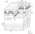
- FIG. 32 is a perspective view of a unit cell of the SJ-SiC-MOSFET 102 of Embodiment 2.
- FIG. The SJ-SiC-MOSFET 101 of the first embodiment is a trench MOSFET, but the SJ-SiC-MOSFET 102 is a planar MOSFET. That is, the SJ-SiC-MOSFET 102 is obtained by applying the characteristic configuration of the SJ-SiC-MOSFET 101 described in the first embodiment to a planar MOSFET.
- the SJ-SiC-MOSFET 102 differs from the SJ-SiC-MOSFET 101 only in the configuration of the MOSFET region 91 .
- the MOSFET region 91 of the SJ-SiC-MOSFET 102 will be described below.
- the p-type body regions 32 and the n-type JFET regions 22 are alternately arranged on the SJ regions 90 .
- the body regions 32 extend along the y-axis direction and are arranged in plurality along the x-axis direction at a repetition period d21.
- the repetition period d2 of the BPW region 31 is referred to as the second repetition period in the first embodiment
- the repetition period d21 of the body region 32 is referred to as the second repetition period in the second embodiment.
- the repetition period d21 of the body regions 32 is shorter than the repetition period d1 of the second pillar regions 30 .
- JFET regions 22 are disposed between body regions 32 .
- An n-type source region 23 is formed in the surface layer of the body region 32 .
- a p-type body contact region 33 extends from the upper surface of the source region 23 through the source region 23 to reach the body region 32 .
- a surface layer of body region 32 sandwiched between JFET region 22 and source region 23 is defined as a channel region.
- a gate electrode 60 is formed on the channel region and JFET region 22 with a gate insulating film 50 interposed therebetween. The above is the configuration of the MOSFET region 91 .
- the gate electrode 60 is covered with an interlayer insulating film 51 and insulated from the source electrode 80 .
- a contact hole is formed in gate insulating film 50 and interlayer insulating film 51 .
- a source electrode 80 is formed inside the contact hole and on interlayer insulating film 51 .
- Source electrode 80 is in ohmic contact with body contact region 33 and source region 23 via first ohmic contact region 70 inside the contact hole.
- MOSFET region 91 of SJ-SiC-MOSFET 102 does not comprise trench 55 , BPW region 31 and connection region 34 unlike SJ-SiC-MOSFET 101 .
- a relatively high concentration body region 32 is directly connected to the second pillar region 30 .
- a crossing region 92 is an intersection of the body region 32 and the second pillar region 30 . Therefore, the sheet resistance Rptot in the conduction path of holes from the intersection region 92 to the source electrode 80 can be kept small. Therefore, the effects of the present technology can be enjoyed to some extent without adding a special structure.
- the method of manufacturing the SJ-SiC-MOSFET 102 is generally the same as the method of manufacturing the SJ-SiC-MOSFET 101 described in the first embodiment.
- the process up to growing an n-type epitaxial region is the same as in the first embodiment.
- the steps of forming the body region 32, the JFET region 22, the source region 23, and the body contact region 33 by a photolithography process, an ion implantation process, and an activation annealing process are the same as in the first embodiment. be.
- a high-quality gate insulating film 50 is formed by thermal oxidation. Subsequent steps are the same as those of the first embodiment.
- FIG. 33 is a perspective view of a unit cell of the SJ-SiC-MOSFET 102A of the first modified example of the second embodiment.
- the SJ-SiC-MOSFET 102A differs from the SJ-SiC-MOSFET 102 in that the body contact region 33 penetrates the body region 32 and reaches the SJ region 90.
- the body contact region 33 also functions as the connection region 34 of the first embodiment, which connects the second pillar region 30 and the body region 32 .
- the surface resistance of the conduction path of holes from the second pillar region 30 to the source electrode 80 is reduced.
- R_ptot can be made smaller. As a result, the electric field applied to the gate insulating film 50 can be reduced.
- the impurity concentration of the body contact region 33 may be the same or different between the lower portion and the upper portion contacting the SJ region 90 .
- FIG. 34 is a perspective view of a unit cell of the SJ-SiC-MOSFET 102B of the second modified example of the second embodiment.
- body region 32 and second pillar region 30 are not connected.
- the body contact region 33 penetrates the body region 32 to protrude from the bottom surface of the body region 32 and connect with the second pillar region 30 to form the intersection region 92 . That is, the lower portion of body contact region 33 protruding from the lower surface of body region 32 has the function of connection region 34 in the first embodiment.
- the lower part of the body contact region 33 is striped and adjacent to the JFET region 22 . According to this configuration, switching loss can be reduced because the body region 32 and the second pillar region 30 are connected by the body contact region 33 having a high impurity concentration. In addition, since the lower part of the body contact region 33 functioning as the connection region 34 is adjacent to the JFET region 22, the JFET resistance can be reduced, and the on-resistance can be further reduced.
- the impurity concentration of the body contact region 33 may be the same or different between the lower portion and the upper portion in contact with the JFET region 22 .
- FIG. 35 is a perspective view of a unit cell of the SJ-SiC-MOSFET 102C of the third modified example of the second embodiment.
- body contact region 33 protrudes from the lower surface of body region 32 only at the upper portion of second pillar region 30 and is connected to second pillar region 30 to form intersection region 92 .
- the body contact region 33 does not protrude from the bottom surface of the body region 32 above the first pillar region 21 .
- the SJ-SiC-MOSFET 102C has the same configuration as the SJ-SiC-MOSFET 102B.
- the area occupation ratio of the JFET region 22 in the xy plane is larger than that of the SJ-SiC-MOSFET 102B, so the on-resistance can be reduced.
- the body region 32 and the second pillar region 30 are connected by the body contact region 33 with a high impurity concentration, so that Rptot can be kept low.
- the impurity concentration of the body contact region 33 may be the same or different between the lower portion and the upper portion in contact with the JFET region 22 .
- MOSFET regions 91 and SJ regions 90 are connected in all intersection regions 92 .
- the MOSFET regions 91 and SJ regions 90 do not need to be connected at all the intersection regions 92 as long as the Rptot is kept low when viewed from a macroscopic point of view and is uniform throughout the active region.
- 80% or more of the intersection regions 92 may be connected directly or via the connection regions 34 or the body contact regions 33 .
- the on-resistance may be further reduced by a method such as forming the JFET region 22 in the intersection region 92 where the MOSFET region 91 and the SJ region 90 are not connected.
- the SJ-SiC-MOSFET has been described as an example of the silicon carbide semiconductor device having both the SJ structure and the MOSFET structure, but the technology of the present disclosure can also be applied to IGBTs in addition to MOSFETs. is possible.
- an emitter electrode, a collector electrode and an emitter region are used instead of the source electrode, the drain electrode and the source region.
- a p-type collector layer is provided between silicon carbide substrate 10 and the drain electrode.
- SJ-SiC-MOSFET 102 which is the silicon carbide semiconductor device of the second embodiment, includes n-type silicon carbide substrate 10, SJ region 90 made of silicon carbide, and MOSFET region 91 provided on the upper surface of SJ region 90.
- Silicon carbide substrate 10 has a first main surface and a second main surface facing each other.
- SJ region 90 is provided on the first main surface of silicon carbide substrate 10 .
- the SJ regions 90 extend in the x-axis direction, which is the first direction parallel to the first main surface, and are alternately arranged in the y-axis direction, which is the second direction parallel to the first main surface and perpendicular to the first direction.
- MOSFET region 91 includes a plurality of body regions 32 made of p-type silicon carbide, a plurality of JFET regions 22 made of n-type silicon carbide, and a plurality of source regions 23 made of n-type silicon carbide, which are impurity regions. , a plurality of body contact regions 33 made of p-type silicon carbide, and a plurality of gate electrodes 60 provided on each body region 32 between each source region 23 and each JFET region 22 with a gate insulating film 50 interposed therebetween. And prepare.
- Each body region 32 extends in the y-axis direction, is arranged in the x-axis direction at a second repetition period d21 shorter than the first repetition period d1 of the second pillar regions 30, and is connected to each second pillar region.
- Each JFET region 22 is provided between each body region 32 .
- Each source region 23 is provided in the surface layer of each body region 32 .
- Each body contact region 33 extends from the upper surface of each source region 23 through each source region 23 to reach each body region 32 and has a lower resistivity than each body region 32 .
- a plurality of gate electrodes 60 are provided on each body region 32 between each source region 23 and each JFET region 22 via a gate insulating film 50 .
- SJ-SiC-MOSFET 102 includes source electrode 80 which is an upper surface electrode provided on multiple body contact regions 33 and drain electrode 83 which is a lower surface electrode formed on the second main surface of silicon carbide substrate 10 .
- source electrode 80 which is an upper surface electrode provided on multiple body contact regions 33
- drain electrode 83 which is a lower surface electrode formed on the second main surface of silicon carbide substrate 10 .
- Embodiment 3 The present embodiment applies the silicon carbide semiconductor devices according to the above-described first and second embodiments to a power converter.
- Application of the silicon carbide semiconductor devices according to the first and second embodiments is not limited to a specific power converter, but hereinafter, as a third embodiment, the first and second embodiments will be applied to a three-phase inverter. A case where a silicon carbide semiconductor device is applied will be described.
- FIG. 36 is a block diagram showing the configuration of a power conversion system to which the power conversion device according to this embodiment is applied.
- the power conversion system shown in FIG. 36 includes a power supply 100, a power conversion device 200 and a load 300.
- the power supply 100 is a DC power supply and supplies DC power to the power converter 200 .
- Power supply 100 can be configured in a variety of ways.
- the power supply 100 can be composed of, for example, a DC system, a solar battery, a storage battery, or a rectifier circuit or an AC/DC converter connected to an AC system.
- the power supply 100 can also be configured by a DC/DC converter that converts DC power output from a DC system into predetermined power.
- the power conversion device 200 is a three-phase inverter connected between the power supply 100 and the load 300 , converts the DC power supplied from the power supply 100 into AC power, and supplies the AC power to the load 300 .
- the power conversion device 200 includes a main conversion circuit 201 that converts DC power into AC power and outputs it, and a drive circuit 202 that outputs a drive signal for driving each switching element of the main conversion circuit 201. , and a control circuit 203 that outputs a control signal for controlling the drive circuit 202 to the drive circuit 202 .
- the load 300 is a three-phase electric motor driven by AC power supplied from the power converter 200 .
- the load 300 is not limited to a specific application, and is an electric motor mounted on various electrical equipment, such as a hybrid vehicle, an electric vehicle, a railroad vehicle, an elevator, or an electric motor for an air conditioner.
- the main conversion circuit 201 includes a switching element and a freewheeling diode (not shown). By switching the switching element, the DC power supplied from the power supply 100 is converted into AC power and supplied to the load 300 .
- the main conversion circuit 201 is a two-level three-phase full bridge circuit, and has six switching elements and It can consist of six freewheeling diodes in anti-parallel.
- the silicon carbide semiconductor device according to any one of the first and second embodiments described above is applied to each switching element of main conversion circuit 201 .
- each upper and lower arm forms each phase (U phase, V phase, W phase) of the full bridge circuit.
- Output terminals of the upper and lower arms, that is, three output terminals of the main conversion circuit 201 are connected to the load 300 .
- the drive circuit 202 generates a drive signal for driving the switching element of the main converter circuit 201 and supplies it to the control electrode of the switching element of the main converter circuit 201 .
- a drive signal for turning on the switching element and a drive signal for turning off the switching element are output to the control electrode of each switching element.
- the driving signal is a voltage signal (ON signal) equal to or higher than the threshold voltage of the switching element, and when maintaining the switching element in the OFF state, the driving signal is a voltage equal to or less than the threshold voltage of the switching element. signal (off signal).
- the control circuit 203 controls the switching elements of the main conversion circuit 201 so that the desired power is supplied to the load 300 . Specifically, based on the power to be supplied to the load 300, the time (on time) during which each switching element of the main conversion circuit 201 should be in the ON state is calculated. For example, the main conversion circuit 201 can be controlled by PWM control that modulates the ON time of the switching element according to the voltage to be output. Then, a control command (control signal) is output to the drive circuit 202 so that an ON signal is output to the switching element that should be in the ON state at each time point, and an OFF signal is output to the switching element that should be in the OFF state. The drive circuit 202 outputs an ON signal or an OFF signal as a drive signal to the control electrode of each switching element according to this control signal.
- the silicon carbide semiconductor devices according to the first and second embodiments are applied as switching elements of the main conversion circuit 201, so reliability and conversion efficiency are improved.
- the silicon carbide semiconductor devices according to Embodiments 1 and 2 to a two-level three-phase inverter has been described.
- the present invention is not limited to this, and can be applied to various power converters.
- a two-level power conversion device is used, but a three-level or multi-level power conversion device may be used.
- the silicon carbide semiconductor device according to 1 and 2 may be applied.
- the silicon carbide semiconductor devices according to the first and second embodiments can be applied to a DC/DC converter or an AC/DC converter.
- the power conversion device to which the silicon carbide semiconductor device according to the first and second embodiments is applied is not limited to the case where the above-described load is an electric motor, and for example, an electric discharge machine, a laser processing machine, or an induction heating cooking machine. It can also be used as a power supply device for a device or a contactless power supply system, and can also be used as a power conditioner for a photovoltaic power generation system, an electric storage system, or the like.
Landscapes
- Electrodes Of Semiconductors (AREA)
- Chemical & Material Sciences (AREA)
- Composite Materials (AREA)
- Junction Field-Effect Transistors (AREA)
Abstract
Description
<A-1.構成>
まず、実施の形態1にかかる炭化珪素半導体装置の構成を説明する。
SJ-SiC-MOSFET101の製造方法について説明する。まず、SJ領域90の形成方法について述べる。上記のとおり、SJの形成方法にはマルチエピ方式と埋め込みエピ方式とがあり、いずれの方法を用いてもよい。
次に、SJ-SiC-MOSFET101の動作について説明する。以下、半導体材料が4H型の炭化珪素であるSJ-SiC-MOSFET101を例に説明する。パワーデバイスはインバータ等の電力変換機器内で様々な動作をするが、SJ-SiC-MOSFET101が効果を発揮する動作および状態として、オフ状態、オン状態およびスイッチング動作(ターンオン、ターンオフ)について説明する。
まず、nチャネル型SJ-MOSFETに共通の一般的なオフ状態について述べる。オフ状態において、ゲート電圧は閾値以下、一般的に0Vまたはマイナス数Vであり、nチャネルが形成されておらず高抵抗状態となっている。インバータではこのオフ状態のときに、素子のドレインに高電圧がかかる。ドレインに正電圧が印加されると、SJ領域90において第1ピラー領域21および第2ピラー領域30の間のpn接合に逆バイアスが印加される。そのため、SJ領域90の横方向に向かって空乏層が伸びていく。ドレイン電圧がある値を超えると、第1ピラー領域21および第2ピラー領域30が完全に空乏化する。これにより、ドレイン-ソース間が大幅に高抵抗化し、オフ状態を維持できる。この時、チャージバランスが完全でないと、どちらかが完全空乏化してももう片方は完全空乏化しないため、電界が余計に生じてしまう。




オン状態では、ゲート電極60に閾値以上の正電圧、例えば15V程度の電圧が印加される。この時、ゲート絶縁膜50直下のチャネル領域、すなわち、n型のJFET領域22とソース領域23に挟まれたボディ領域32とゲート絶縁膜50の界面に、n型の反転層チャネルが誘起される。これにより、ソース領域23とJFET領域22が低抵抗で接続され、結果、ドレイン電極83とソース電極80が低抵抗で接続される。



次に、スイッチング動作のうちターンオフについて述べる。ターンオフは、オン電流を低抵抗で流していた状態から、ゲート電圧が閾値以下、例えば0または-10Vなどの電圧に切り替わることにより、nチャネルが消失しオフ状態となる動作である。この時にドレイン電圧が急速に増大し、その後電流がゼロ近傍に低下していく。








次に、スイッチング動作のうちターンオンについて述べる。ターンオンは、高抵抗状態のMOSFETに負荷電圧VLが印加された状態から、ゲート電圧が閾値以上、例えば15Vなどの電圧に切り替わることにより、nチャネルが誘起され、MOSFETがオン状態となる動作である。この時にドレイン電流が急速に増大し、その後電圧がオン電圧近傍に低下していく。
図18は、実施の形態1の第1変形例のSJ-SiC-MOSFET101Aのユニットセルの斜視図である。SJ-SiC-MOSFET101Aは、p型の接続領域34が、第2ピラー領域30の上部のBPW領域31に対してだけでなく、第1ピラー領域21の上部のBPW領域31に対しても設けられる点で、SJ-SiC-MOSFET101と異なる。つまり、第1ピラー領域21の上部のBPW領域31は、接続領域34を介してボディ領域32と接続する。これにより、n型の第1ピラー領域21における電界の変動によりBPW領域31へ流れる電流を、SJピラーの充放電とは別に流すことができるため、ゲート絶縁膜50にかかる電界が低減する。
実施の形態1の炭化珪素半導体装置であるSJ-SiC-MOSFET101は、n型の炭化珪素基板10と、炭化珪素からなるSJ領域90と、SJ領域90の上面上に設けられたMOSFET領域91とを備える。炭化珪素基板10は、互いに対向する第1主面および第2主面を有する。SJ領域90は、炭化珪素基板10の第1主面上に設けられる。SJ領域90は、第1主面と平行な第1方向であるx軸方向に伸長し、第1主面と平行かつ第1方向に垂直な第2方向であるy軸方向に交互に配列された、n型の複数の第1ピラー領域21およびp型の複数の第2ピラー領域30を備える。MOSFET領域91は、p型の炭化珪素からなる複数のBPW領域31と、複数のゲート電極60と、n型の炭化珪素からなる複数のJFET領域22と、p型の炭化珪素からなる複数のボディ領域32と、p型の炭化珪素からなる複数のボディコンタクト領域33と、n型の炭化珪素からなる複数の不純物領域であるソース領域23と、p型の炭化珪素からなる少なくとも1つの接続領域34とを備える。各BPW領域31は、y軸方向に伸長し、x軸方向に、第2ピラー領域30の繰り返し周期である第1繰り返し周期d1より短い第2繰り返し周期d2で配列され、第2ピラー領域30に接続される。各ゲート電極60は、各BPW領域31の上にy軸方向に設けられた各トレンチ55内にゲート絶縁膜50を介して設けられる。各JFET領域22は、隣り合う2つのBPW領域31の間、および隣り合う2つのトレンチ55の間でy軸方向に伸長する。各ボディ領域32は、各JFET領域22の上に各JFET領域22に接して設けられる。各ボディコンタクト領域33は、各ボディ領域32の上に設けられ、各ボディ領域32より抵抗率が低い。ソース領域23は、各ボディ領域32の上に各トレンチ55および各ボディコンタクト領域33の夫々に接して設けられる。少なくとも1つの接続領域34は、少なくとも1つのJFET領域22に接し、少なくとも1つのBPW領域31と少なくとも1つのボディ領域32とを接続する。SJ-SiC-MOSFET101は、各ボディコンタクト領域33上に設けられる上面電極であるソース電極80と、炭化珪素基板10の第2主面上に設けられる下面電極であるドレイン電極83とを備える。以上の構成により、第2ピラー領域30への低抵抗なコンタクトが実現し、耐圧のばらつきが抑制され、チャネル抵抗およびJFET抵抗が低減する。
<B-1.構成>
図32は、実施の形態2のSJ-SiC-MOSFET102のユニットセルの斜視図である。実施の形態1のSJ-SiC-MOSFET101はトレンチ型のMOSFETであったが、SJ-SiC-MOSFET102はプレーナ型のMOSFETである。つまり、SJ-SiC-MOSFET102は実施の形態1で説明したSJ-SiC-MOSFET101の特徴的な構成をプレーナ型のMOSFETに適用したものである。
SJ-SiC-MOSFET102の製造方法は、概ね実施の形態1で説明したSJ-SiC-MOSFET101の製造方法と同様である。炭化珪素基板10上にSJ領域90を形成した後、さらにn型のエピ領域を成長させるところまでは実施の形態1と同様である。その後、構造は異なるが、フォトリソグラフィ工程、イオン注入工程、および活性化アニール工程によってボディ領域32、JFET領域22、ソース領域23、ボディコンタクト領域33を形成するところも、実施の形態1と同様である。トレンチエッチング、BPW領域31、接続領域34を形成する工程は存在しない。その後、熱酸化により高品質なゲート絶縁膜50を形成する。その後の工程は、実施の形態1と同様である。
図33は、実施の形態2の第1変形例のSJ-SiC-MOSFET102Aのユニットセルの斜視図である。SJ-SiC-MOSFET102Aは、ボディコンタクト領域33がボディ領域32を貫通してSJ領域90に達する点でSJ-SiC-MOSFET102と異なる。これにより、ボディコンタクト領域33が第2ピラー領域30とボディ領域32とを接続する、実施の形態1の接続領域34の機能を兼ねることになる。第2ピラー領域30とボディ領域32とが、p型不純物濃度の高いボディコンタクト領域33を用いて接続されることにより、第2ピラー領域30からソース電極80への正孔の通電経路における面抵抗Rptotを小さくすることができる。その結果、ゲート絶縁膜50にかかる電界を低減できる。
実施の形態2の炭化珪素半導体装置であるSJ-SiC-MOSFET102は、n型の炭化珪素基板10と、炭化珪素からなるSJ領域90と、SJ領域90の上面上に設けられたMOSFET領域91とを備える。炭化珪素基板10は、互いに対向する第1主面および第2主面を有する。SJ領域90は、炭化珪素基板10の第1主面上に設けられる。SJ領域90は、第1主面と平行な第1方向であるx軸方向に伸長し、第1主面と平行かつ第1方向に垂直な第2方向であるy軸方向に交互に配列された、n型の複数の第1ピラー領域21およびp型の複数の第2ピラー領域30を備える。MOSFET領域91は、p型の炭化珪素からなる複数のボディ領域32と、n型の炭化珪素からなる複数のJFET領域22と、n型の炭化珪素からなる複数の不純物領域であるソース領域23と、p型の炭化珪素からなる複数のボディコンタクト領域33と、各ソース領域23と各JFET領域22との間の各ボディ領域32上にゲート絶縁膜50を介して設けられた複数のゲート電極60と、を備える。各ボディ領域32は、y軸方向に伸長し、x軸方向に第2ピラー領域30の第1繰り返し周期d1より短い第2繰り返し周期d21で配列され、各第2ピラー領域に接続される。各JFET領域22は、各ボディ領域32の間に設けられる。各ソース領域23は、各ボディ領域32の表層に設けられる。各ボディコンタクト領域33は、各ソース領域23の上面から各ソース領域23を貫通して各ボディ領域32に達し、各ボディ領域32より抵抗率が低い。複数のゲート電極60は、各ソース領域23と各JFET領域22との間の各ボディ領域32上にゲート絶縁膜50を介して設けられる。SJ-SiC-MOSFET102は、複数のボディコンタクト領域33上に設けられた上面電極であるソース電極80と、炭化珪素基板10の第2主面上に形成される下面電極であるドレイン電極83とを備える。以上の構成により、第2ピラー領域30への低抵抗なコンタクトが実現し、耐圧のばらつきが抑制され、チャネル抵抗およびJFET抵抗が低減する。
本実施の形態は、上述した実施の形態1,2にかかる炭化珪素半導体装置を電力変換装置に適用したものである。実施の形態1,2にかかる炭化珪素半導体装置の適用は特定の電力変換装置に限定されるものではないが、以下、実施の形態3として、三相のインバータに実施の形態1,2にかかる炭化珪素半導体装置を適用した場合について説明する。
Claims (17)
- 互いに対向する第1主面および第2主面を有するn型の炭化珪素基板と、
前記炭化珪素基板の前記第1主面上に設けられる炭化珪素からなるSJ領域と、
前記SJ領域の上面上に設けられるMOSFET領域とを備え、
前記SJ領域は、前記第1主面と平行な第1方向に伸長し、前記第1主面と平行かつ前記第1方向に垂直な第2方向に交互に配列された、n型の複数の第1ピラー領域およびp型の複数の第2ピラー領域を備え、
前記MOSFET領域は、
前記第2方向に伸長し、前記第1方向に、前記第2ピラー領域の繰り返し周期である第1繰り返し周期より短い第2繰り返し周期で配列され、前記第2ピラー領域に接続される、p型の炭化珪素からなる複数のBPW領域と、
各前記BPW領域の上に前記第2方向に設けられる各トレンチ内にゲート絶縁膜を介して設けられる複数のゲート電極と、
隣り合う2つの前記BPW領域の間、および隣り合う2つの前記トレンチの間で前記第2方向に伸長する、n型の炭化珪素からなる複数のJFET領域と、
各前記JFET領域の上に各前記JFET領域に接して設けられる、p型の炭化珪素からなる複数のボディ領域と、
各前記ボディ領域の上に設けられる各前記ボディ領域より抵抗率が低いp型の炭化珪素からなる複数のボディコンタクト領域と、
各前記ボディ領域の上に各前記トレンチおよび各前記ボディコンタクト領域の夫々に接して設けられるn型の炭化珪素からなる複数の不純物領域と、
少なくとも1つの前記JFET領域に接し、少なくとも1つの前記BPW領域と少なくとも1つの前記ボディ領域とを接続するp型の炭化珪素からなる少なくとも1つの接続領域とを備え、
各前記ボディコンタクト領域上に設けられる上面電極と、
前記炭化珪素基板の前記第2主面上に設けられる下面電極とを備える、
炭化珪素半導体装置。 - 各前記第2ピラー領域と各前記BPW領域とが直接接続される、
請求項1に記載の炭化珪素半導体装置。 - 前記少なくとも1つの接続領域は、各前記JFET領域に接し、各前記BPW領域と各前記ボディ領域とを接続する複数の接続領域であり、
各前記第2ピラー領域と各前記BPW領域とが各前記接続領域を介して接続される、
請求項1に記載の炭化珪素半導体装置。 - 前記少なくとも1つの接続領域は、各前記JFET領域に接し、各前記BPW領域と各前記ボディ領域とを接続する複数の接続領域であり、
前記複数の接続領域は、各前記第1ピラー領域上に設けられる接続領域を含む、
請求項1から請求項3のいずれか1項に記載の炭化珪素半導体装置。 - 前記少なくとも1つの接続領域は、各前記JFET領域に接し、各前記BPW領域と各前記ボディ領域とを接続する複数の接続領域であり、
各前記接続領域は、各前記トレンチの片側の側面の全体に接して設けられる、
請求項1から請求項4のいずれか1項に記載の炭化珪素半導体装置。 - 前記少なくとも1つの接続領域は、各前記JFET領域に接し、各前記BPW領域と各前記ボディ領域とを接続する複数の接続領域であり、
前記複数の接続領域は、一部の前記トレンチに対しては、前記トレンチの両側の側面の全体に接して設けられ、他の一部の前記トレンチに対しては、前記トレンチの下部の前記BPW領域と前記第2ピラー領域との交差部にのみ設けられる、
請求項1から請求項3のいずれか1項に記載の炭化珪素半導体装置。 - 前記複数の第2ピラー領域と前記複数のBPW領域との交差点のうち80%以上の数の交差点において、各前記第2ピラー領域と各前記BPW領域とが直接接続される、
請求項1から請求項6のいずれか1項に記載の炭化珪素半導体装置。 - 前記少なくとも1つの接続領域は、各前記JFET領域に接し、各前記BPW領域と各前記ボディ領域とを接続する複数の接続領域であり、
前記複数の第2ピラー領域と前記複数のBPW領域との交差点のうち80%以上の数の交差点において、各前記第2ピラー領域と各前記BPW領域とが各前記接続領域を介して接続される、
請求項1から請求項6のいずれか1項に記載の炭化珪素半導体装置。 - 各前記JFET領域のn型不純物濃度は、各前記第1ピラー領域のn型不純物濃度より高い、
請求項1から請求項8のいずれか1項に記載の炭化珪素半導体装置。 - 前記第1主面と平行な平面における前記少なくとも1つの接続領域の面積占有率が25%以下である、
請求項1から請求項9のいずれか1項に記載の炭化珪素半導体装置。 - 前記少なくとも1つの接続領域のp型不純物濃度が4×1017cm-3以上である、
請求項1から請求項10のいずれか1項に記載の炭化珪素半導体装置。 - 互いに対向する第1主面および第2主面を有するn型の炭化珪素基板と、
前記炭化珪素基板の前記第1主面上に設けられる炭化珪素からなるSJ領域と、
前記SJ領域の上面上に設けられるMOSFET領域とを備え、
前記SJ領域は、前記第1主面と平行な第1方向に伸長し、前記第1主面と平行かつ前記第1方向と垂直な第2方向に交互に配列された、n型の複数の第1ピラー領域およびp型の複数の第2ピラー領域を備え、
前記MOSFET領域は、
前記第2方向に伸長し、前記第1方向に、前記第2ピラー領域の繰り返し周期である第1繰り返し周期より短い第2繰り返し周期で配列され、各前記第2ピラー領域に接続される、p型の炭化珪素からなる複数のボディ領域と、
各前記ボディ領域の間に設けられるn型の炭化珪素からなる複数のJFET領域と、
各前記ボディ領域の表層に設けられるn型の炭化珪素からなる複数の不純物領域と、
各前記不純物領域の上面から各前記不純物領域を貫通して各前記ボディ領域に達する、各前記ボディ領域より抵抗率が低いp型の炭化珪素からなる複数のボディコンタクト領域と、
各前記不純物領域と各前記JFET領域との間の各前記ボディ領域上にゲート絶縁膜を介して設けられる複数のゲート電極と、を備え、
前記複数のボディコンタクト領域上に設けられる上面電極と、
前記炭化珪素基板の前記第2主面上に設けられる下面電極とを備える、
炭化珪素半導体装置。 - 各前記第2ピラー領域と各前記ボディ領域とが直接接続される、
請求項12に記載の炭化珪素半導体装置。 - 各前記ボディコンタクト領域は各前記ボディ領域を貫通して各前記第2ピラー領域と接触し、
各前記第2ピラー領域と各前記ボディ領域とが各前記ボディコンタクト領域を介して接続される、
請求項12に記載の炭化珪素半導体装置。 - 前記複数の第2ピラー領域と前記複数のボディ領域との交差点のうち80%以上の数の交差点において、各前記第2ピラー領域と各前記ボディ領域とが直接接続される、
請求項1から請求項14のいずれか1項に記載の炭化珪素半導体装置。 - 前記複数の第2ピラー領域と前記複数のボディ領域との交差点のうち80%以上の数の交差点において、各前記第2ピラー領域と各前記ボディ領域とが各前記ボディコンタクト領域を介して接続される、
請求項1から請求項14のいずれか1項に記載の炭化珪素半導体装置。 - 請求項1から請求項16のいずれか1項に記載の炭化珪素半導体装置を有し、入力される電力を変換して出力する主変換回路と、
前記炭化珪素半導体装置を駆動する駆動信号を前記炭化珪素半導体装置に出力する駆動回路と、
前記駆動回路を制御する制御信号を前記駆動回路に出力する制御回路と、を備える、
電力変換装置。
Priority Applications (5)
| Application Number | Priority Date | Filing Date | Title |
|---|---|---|---|
| US18/576,761 US20240290830A1 (en) | 2021-07-15 | 2021-07-15 | Silicon carbide semiconductor device and electric power converter |
| JP2023534538A JP7625086B2 (ja) | 2021-07-15 | 2021-07-15 | 炭化珪素半導体装置および電力変換装置 |
| DE112021007977.8T DE112021007977T5 (de) | 2021-07-15 | 2021-07-15 | Siliciumcarbid-halbleitereinrichtung und elektrischer stromrichter |
| CN202180100410.1A CN117693822A (zh) | 2021-07-15 | 2021-07-15 | 碳化硅半导体装置以及电力变换装置 |
| PCT/JP2021/026592 WO2023286235A1 (ja) | 2021-07-15 | 2021-07-15 | 炭化珪素半導体装置および電力変換装置 |
Applications Claiming Priority (1)
| Application Number | Priority Date | Filing Date | Title |
|---|---|---|---|
| PCT/JP2021/026592 WO2023286235A1 (ja) | 2021-07-15 | 2021-07-15 | 炭化珪素半導体装置および電力変換装置 |
Publications (1)
| Publication Number | Publication Date |
|---|---|
| WO2023286235A1 true WO2023286235A1 (ja) | 2023-01-19 |
Family
ID=84919774
Family Applications (1)
| Application Number | Title | Priority Date | Filing Date |
|---|---|---|---|
| PCT/JP2021/026592 Ceased WO2023286235A1 (ja) | 2021-07-15 | 2021-07-15 | 炭化珪素半導体装置および電力変換装置 |
Country Status (5)
| Country | Link |
|---|---|
| US (1) | US20240290830A1 (ja) |
| JP (1) | JP7625086B2 (ja) |
| CN (1) | CN117693822A (ja) |
| DE (1) | DE112021007977T5 (ja) |
| WO (1) | WO2023286235A1 (ja) |
Cited By (1)
| Publication number | Priority date | Publication date | Assignee | Title |
|---|---|---|---|---|
| WO2025211288A1 (ja) * | 2024-04-05 | 2025-10-09 | 富士電機株式会社 | 半導体装置 |
Families Citing this family (1)
| Publication number | Priority date | Publication date | Assignee | Title |
|---|---|---|---|---|
| CN120111920B (zh) * | 2025-02-25 | 2026-04-17 | 中国科学院微电子研究所 | 一种抗辐射加固设计的四端子SiC MOSFET器件及其制造方法 |
Citations (5)
| Publication number | Priority date | Publication date | Assignee | Title |
|---|---|---|---|---|
| JP2003229569A (ja) * | 2002-01-31 | 2003-08-15 | Fuji Electric Co Ltd | 超接合半導体素子の製造方法 |
| JP2004356577A (ja) * | 2003-05-30 | 2004-12-16 | Denso Corp | 半導体装置の製造方法および半導体基板ならびにそれらにより製造される半導体装置 |
| JP2008159601A (ja) * | 2005-11-28 | 2008-07-10 | Fuji Electric Device Technology Co Ltd | 半導体装置および半導体装置の製造方法 |
| JP2008283151A (ja) * | 2007-05-14 | 2008-11-20 | Denso Corp | 半導体装置およびその製造方法 |
| JP2019510376A (ja) * | 2016-03-22 | 2019-04-11 | ゼネラル・エレクトリック・カンパニイ | 高速スイッチング機能を有する超接合パワー半導体デバイス |
Family Cites Families (1)
| Publication number | Priority date | Publication date | Assignee | Title |
|---|---|---|---|---|
| JPS6377302U (ja) | 1986-11-07 | 1988-05-23 |
-
2021
- 2021-07-15 JP JP2023534538A patent/JP7625086B2/ja active Active
- 2021-07-15 DE DE112021007977.8T patent/DE112021007977T5/de active Pending
- 2021-07-15 WO PCT/JP2021/026592 patent/WO2023286235A1/ja not_active Ceased
- 2021-07-15 CN CN202180100410.1A patent/CN117693822A/zh active Pending
- 2021-07-15 US US18/576,761 patent/US20240290830A1/en active Pending
Patent Citations (5)
| Publication number | Priority date | Publication date | Assignee | Title |
|---|---|---|---|---|
| JP2003229569A (ja) * | 2002-01-31 | 2003-08-15 | Fuji Electric Co Ltd | 超接合半導体素子の製造方法 |
| JP2004356577A (ja) * | 2003-05-30 | 2004-12-16 | Denso Corp | 半導体装置の製造方法および半導体基板ならびにそれらにより製造される半導体装置 |
| JP2008159601A (ja) * | 2005-11-28 | 2008-07-10 | Fuji Electric Device Technology Co Ltd | 半導体装置および半導体装置の製造方法 |
| JP2008283151A (ja) * | 2007-05-14 | 2008-11-20 | Denso Corp | 半導体装置およびその製造方法 |
| JP2019510376A (ja) * | 2016-03-22 | 2019-04-11 | ゼネラル・エレクトリック・カンパニイ | 高速スイッチング機能を有する超接合パワー半導体デバイス |
Cited By (1)
| Publication number | Priority date | Publication date | Assignee | Title |
|---|---|---|---|---|
| WO2025211288A1 (ja) * | 2024-04-05 | 2025-10-09 | 富士電機株式会社 | 半導体装置 |
Also Published As
| Publication number | Publication date |
|---|---|
| CN117693822A (zh) | 2024-03-12 |
| JPWO2023286235A1 (ja) | 2023-01-19 |
| US20240290830A1 (en) | 2024-08-29 |
| DE112021007977T5 (de) | 2024-05-02 |
| JP7625086B2 (ja) | 2025-01-31 |
Similar Documents
| Publication | Publication Date | Title |
|---|---|---|
| JP6929404B2 (ja) | 炭化珪素半導体装置および電力変換装置 | |
| JP6964950B2 (ja) | 半導体装置および電力変換装置 | |
| US11158704B2 (en) | Semiconductor device and power conversion device | |
| CN111466032B (zh) | 碳化硅半导体装置以及电力变换装置 | |
| CN110366782A (zh) | 碳化硅半导体装置、电力变换装置、碳化硅半导体装置的制造方法以及电力变换装置的制造方法 | |
| WO2019123717A1 (ja) | 炭化珪素半導体装置および電力変換装置 | |
| JP7094439B2 (ja) | 炭化珪素半導体装置および電力変換装置 | |
| JPWO2018084020A1 (ja) | 炭化珪素半導体装置および電力変換装置 | |
| JP6991370B2 (ja) | 半導体装置及び電力変換装置 | |
| JP7778041B2 (ja) | 半導体装置および電力変換装置 | |
| JP2019096631A (ja) | 半導体装置および電力変換装置 | |
| JP6976489B2 (ja) | 炭化珪素半導体装置および電力変換装置 | |
| WO2021106152A1 (ja) | 炭化珪素半導体装置、電力変換装置および炭化珪素半導体装置の製造方法 | |
| JP7625086B2 (ja) | 炭化珪素半導体装置および電力変換装置 | |
| JP7330396B2 (ja) | 半導体装置及び電力変換装置 | |
| JP6377309B1 (ja) | 炭化珪素半導体装置、電力変換装置、炭化珪素半導体装置の製造方法、および電力変換装置の製造方法 | |
| JPWO2019124384A1 (ja) | 炭化珪素半導体装置および電力変換装置 | |
| JP7127748B2 (ja) | 炭化珪素半導体装置、電力変換装置および炭化珪素半導体装置の製造方法 | |
| WO2026094283A1 (ja) | 炭化珪素半導体装置、炭化珪素半導体装置の製造方法、電力変換装置 | |
| WO2024013868A1 (ja) | 半導体装置、および、電力変換装置 | |
| WO2022264212A1 (ja) | 炭化珪素半導体装置および炭化珪素半導体装置を用いた電力変換装置 |
Legal Events
| Date | Code | Title | Description |
|---|---|---|---|
| 121 | Ep: the epo has been informed by wipo that ep was designated in this application |
Ref document number: 21950174 Country of ref document: EP Kind code of ref document: A1 |
|
| ENP | Entry into the national phase |
Ref document number: 2023534538 Country of ref document: JP Kind code of ref document: A |
|
| WWE | Wipo information: entry into national phase |
Ref document number: 18576761 Country of ref document: US |
|
| WWE | Wipo information: entry into national phase |
Ref document number: 202180100410.1 Country of ref document: CN |
|
| WWE | Wipo information: entry into national phase |
Ref document number: 112021007977 Country of ref document: DE |
|
| 122 | Ep: pct application non-entry in european phase |
Ref document number: 21950174 Country of ref document: EP Kind code of ref document: A1 |