WO2023276956A1 - 熱電変換デバイス - Google Patents
熱電変換デバイス Download PDFInfo
- Publication number
- WO2023276956A1 WO2023276956A1 PCT/JP2022/025585 JP2022025585W WO2023276956A1 WO 2023276956 A1 WO2023276956 A1 WO 2023276956A1 JP 2022025585 W JP2022025585 W JP 2022025585W WO 2023276956 A1 WO2023276956 A1 WO 2023276956A1
- Authority
- WO
- WIPO (PCT)
- Prior art keywords
- conversion device
- thermoelectric conversion
- wiring
- thermoelectric
- meander
- Prior art date
- Legal status (The legal status is an assumption and is not a legal conclusion. Google has not performed a legal analysis and makes no representation as to the accuracy of the status listed.)
- Ceased
Links
Images








Classifications
-
- G—PHYSICS
- G01—MEASURING; TESTING
- G01K—MEASURING TEMPERATURE; MEASURING QUANTITY OF HEAT; THERMALLY-SENSITIVE ELEMENTS NOT OTHERWISE PROVIDED FOR
- G01K7/00—Measuring temperature based on the use of electric or magnetic elements directly sensitive to heat ; Power supply therefor, e.g. using thermoelectric elements
- G01K7/36—Measuring temperature based on the use of electric or magnetic elements directly sensitive to heat ; Power supply therefor, e.g. using thermoelectric elements using magnetic elements, e.g. magnets, coils
-
- H—ELECTRICITY
- H10—SEMICONDUCTOR DEVICES; ELECTRIC SOLID-STATE DEVICES NOT OTHERWISE PROVIDED FOR
- H10N—ELECTRIC SOLID-STATE DEVICES NOT OTHERWISE PROVIDED FOR
- H10N15/00—Thermoelectric devices without a junction of dissimilar materials; Thermomagnetic devices, e.g. using the Nernst-Ettingshausen effect
-
- G—PHYSICS
- G01—MEASURING; TESTING
- G01K—MEASURING TEMPERATURE; MEASURING QUANTITY OF HEAT; THERMALLY-SENSITIVE ELEMENTS NOT OTHERWISE PROVIDED FOR
- G01K7/00—Measuring temperature based on the use of electric or magnetic elements directly sensitive to heat ; Power supply therefor, e.g. using thermoelectric elements
- G01K7/02—Measuring temperature based on the use of electric or magnetic elements directly sensitive to heat ; Power supply therefor, e.g. using thermoelectric elements using thermoelectric elements, e.g. thermocouples
Definitions
- the present invention relates to thermoelectric conversion devices.
- Patent Document 1 discloses a film-like heat flux sensor as an example of a thermoelectric conversion device that converts heat into electricity using a temperature difference within a material.
- the heat flux sensor described in Patent Document 1 includes a flexible film-like insulating member having a first surface and a second surface opposite to the first surface, and arranged inside the insulating member.
- thermoelectric members made of a first thermoelectric material; and a second thermoelectric member arranged inside the insulating member and made of a second thermoelectric material different from the first thermoelectric material, wherein the plurality of first thermoelectric members are a plurality of second thermoelectric members arranged alternately with each other; arranged on the first surface side with respect to the plurality of first thermoelectric members and the plurality of second thermoelectric members; of the second thermoelectric members, a plurality of first conductor patterns connecting the first thermoelectric members and the second thermoelectric members arranged side by side, and the plurality of first thermoelectric members and the plurality of second thermoelectric members a plurality of second conductor patterns arranged on the second surface side and connecting the first thermoelectric members and the second thermoelectric members arranged side by side among the plurality of first thermoelectric members and the plurality of second thermoelectric members; Prepare.
- the heat flux sensor described in Patent Document 1 is installed on the measurement surface of the object to be measured with one of the first surface and the second surface in contact with the measurement surface of the object.
- a heat flow passes through the heat flux sensor in a direction from one of the first surface and the second surface of the heat flux sensor to the other.
- a temperature difference occurs between the first surface side and the second surface side of the heat flux sensor. That is, a temperature difference occurs between one side and the other side of each of the first thermoelectric member and the second thermoelectric member that are connected to each other.
- a thermoelectromotive force is generated in the first thermoelectric member and the second thermoelectric member due to the Seebeck effect.
- the heat flux sensor described in Patent Document 1 outputs this thermoelectromotive force, specifically voltage, as a sensor signal.
- the present invention was made to solve the above problems, and an object of the present invention is to provide a thermoelectric conversion device that can obtain a sufficient electromotive force per unit installation area even if the temperature difference is small.
- thermoelectric conversion device of the present invention in a first aspect, comprises a base body including a plurality of laminated substrates, and a meander wiring having a laminated structure provided inside the base body.
- the meander wire includes a thermoelectric material having an anomalous Nernst effect.
- thermoelectric conversion device of the present invention includes a winding core and a winding wound around the winding core.
- the winding includes a thermoelectric material having an anomalous Nernst effect.
- thermoelectric conversion device of the present invention in a third aspect, comprises a plurality of substrates and meander wiring provided on the main surface of each of the substrates.
- the meander wire includes a thermoelectric material having an anomalous Nernst effect.
- the adjacent substrates are arranged at an angle larger than 0 degrees and smaller than 180 degrees.
- thermoelectric conversion device that can obtain a sufficient electromotive force per unit installation area even if the temperature difference is small.
- FIG. 1 is a perspective view schematically showing an example of a thermoelectric conversion device according to a first embodiment of the invention.
- 2 is an exploded perspective view of the thermoelectric conversion device shown in FIG. 1.
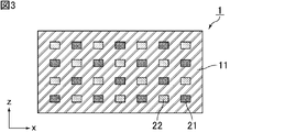
- FIG. 3 is a cross-sectional view of the thermoelectric conversion device shown in FIG. 2 along line III-III.
- FIG. 4 is an exploded perspective view schematically showing a first modification of the thermoelectric conversion device according to the first embodiment of the invention.
- FIG. 5 is an exploded perspective view schematically showing a second modification of the thermoelectric conversion device according to the first embodiment of the invention.
- FIG. 6 is an exploded perspective view schematically showing a third modification of the thermoelectric conversion device according to the first embodiment of the invention.
- FIG. 7 is a perspective view schematically showing an example of a thermoelectric conversion device in the form of a chip according to the first embodiment of the present invention.
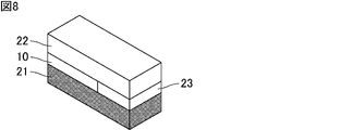
- 8 is an enlarged perspective view of a portion surrounded by a broken line in FIG. 7.
- FIG. 9 is a perspective view schematically showing an example of a state in which via conductors are not provided in the thermoelectric conversion device shown in FIG. 7.
- FIG. 10 is a perspective view schematically showing another example of the thermoelectric conversion device according to the first embodiment of the present invention in the form of a chip.
- FIG. 11 is a perspective view schematically showing an example of a state in which the thermoelectric conversion device shown in FIG. 7 or 10 is singulated.
- FIG. 12 is an exploded perspective view schematically showing a fourth modification of the thermoelectric conversion device according to the first embodiment of the invention.
- FIG. 13 is an exploded perspective view schematically showing a fifth modification of the thermoelectric conversion device according to the first embodiment of the invention.
- FIG. 14 is an exploded perspective view schematically showing a sixth modification of the thermoelectric conversion device according to the first embodiment of the invention.
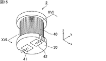
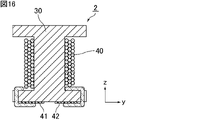
- FIG. 15 is a perspective view schematically showing an example of a thermoelectric conversion device according to the second embodiment of the invention. 16 is a cross-sectional view of the thermoelectric conversion device shown in FIG. 15 along line XVI-XVI.
- FIG. 17 is a perspective view schematically showing an example of a thermoelectric conversion device according to the third embodiment of the invention.
- 18 is an exploded perspective view of the thermoelectric conversion device shown in FIG. 17.
- FIG. 17 is a perspective view schematically showing an example of a thermoelectric conversion device according to the third embodiment of the invention.
- thermoelectric conversion device of the present invention will be described below.
- the present invention is not limited to the following configurations, and can be appropriately modified and applied without changing the gist of the present invention. Combinations of two or more of the individual desirable configurations described below are also part of the present invention.
- thermoelectric conversion device of the present invention the total extension of wiring or windings containing thermoelectric materials can be lengthened. Therefore, the electromotive voltage due to the temperature gradient can be increased.
- thermoelectric conversion device of the present invention is, for example, a chip component. By making the thermoelectric conversion device into a chip structure, the thermoelectric conversion device can be mounted on the electronic substrate by soldering or the like.
- thermoelectric conversion device includes an element body including a plurality of laminated substrates, and a meander wiring having a laminated structure provided inside the element body.
- the meander wire includes a thermoelectric material having an anomalous Nernst effect.
- FIG. 1 is a perspective view schematically showing an example of the thermoelectric conversion device according to the first embodiment of the invention.
- 2 is an exploded perspective view of the thermoelectric conversion device shown in FIG. 1.
- FIG. FIG. 3 is a cross-sectional view of the thermoelectric conversion device shown in FIG. 2 along line III-III. External electrodes are omitted in FIGS.
- thermoelectric conversion device 1 shown in FIG. 1 is a chip component. As shown in FIGS. 2 and 3, the thermoelectric conversion device 1 includes an element body 11 including a plurality of laminated substrates 10, and a meander wiring 20 provided inside the element body 11 and having a laminated structure. . As shown in FIG. 1, the outer shape of the thermoelectric conversion device 1 is, for example, a polygonal prism such as a rectangular parallelepiped.
- the element body 11 is configured by stacking a plurality of substrates 10 in the z-axis direction.
- the base body 11 may include the substrate 10 on which the meander wiring 20 is not provided.
- the number of substrates 10 on which the meander wiring 20 is provided is not particularly limited, it is, for example, 2 or more and 100 or less.
- a meandering wiring means a wiring extending in one direction while meandering.
- the shape of the meander wiring may have angular corners or chamfered corners.
- the meander wiring 20 is provided on the main surface of each substrate 10 and extends in the x-axis direction while meandering. As shown in FIG. 2, the meander wiring 20 is preferably provided on the main surface facing the positive direction among the main surfaces of each substrate 10 facing in the z-axis direction.
- the shape of the meander wiring 20 in plan view may be the same or different between the substrates 10 .
- the meander wiring 20 contains a thermoelectric material having an anomalous Nernst effect.
- the anomalous Nernst effect is a phenomenon in which, when a heat flow is applied to a magnetized magnetic body, a voltage is generated in a direction (cross product direction) perpendicular to the magnetization direction of the magnetic body and the heat flow direction.
- the meander wiring 20 is formed by first wiring 21 made of a thermoelectric material and second wiring made of a conductor, as shown in FIG. It is preferable that the wirings 22 are alternately arranged. Note that the meander wiring 20 may be composed only of the first wiring 21 made of a thermoelectric material.
- thermoelectric material forming the first wiring 21 examples include Fe 3 Sn, Fe 3 Al, Fe 3 Ga, Fe 3 Ge, Co 2 MnGa, Co 2 MnAl, Co 2 MnIn, Mn 3 Ga, Mn 3 Sn, Mn 3 Ge, Fe 2 NiGa, CoTiSb, CoVSb, CoCrSb, CoMnSb, TiGa 2 Mn and the like.
- Examples of conductors that make up the second wiring 22 include Ag, Cu, Au, Ni, and Pt.
- the meander wiring 20 has a laminated structure in the z-axis direction, and is connected between substrates 10 adjacent to each other in the lamination direction (the z-axis direction in FIG. 2). Specifically, the meander wiring 20 between the substrates 10 is electrically connected through via conductors 23 . Therefore, the meander wiring 20 extends in the main surface direction of the substrate 10 and has a laminated structure in the lamination direction of the substrate 10 .
- the meander wiring 20 containing the thermoelectric material having the anomalous Nernst effect between the substrates 10 By connecting the meander wiring 20 containing the thermoelectric material having the anomalous Nernst effect between the substrates 10, the total extension of the wiring containing the thermoelectric material can be lengthened. Therefore, even if the temperature difference is small, a sufficient electromotive force per unit installation area can be obtained.
- the first wiring 21 made of the thermoelectric material has an outer product direction (that is, a y-axis positive direction).
- the meander wiring 20 into a laminated structure to form a chip, the heat radiation from the side walls increases and the temperature difference increases.
- external electrodes 24 and 25 electrically connected to the meander wiring 20 are preferably provided on the surface of the element body 11 .
- the material constituting the substrate 10 is not particularly limited, but a ceramic material with low thermal conductivity and low electrical conductivity is preferable.
- ceramic materials forming the substrate 10 include aluminum nitride, boron nitride, silicon carbide, alumina, spinel-type oxides, perovskite-type oxides, and the like.
- the material forming the substrate 10 may be a ceramic material, a glass material, or a resin material.
- a low-temperature co-fired ceramic material is preferred so as not to change the ordered phase of the thermoelectric material.
- Low-temperature co-fired ceramic materials include, for example, composite materials containing borosilicate glass and alumina.
- the ceramic material forming the substrate 10 has a low thermal conductivity.
- the ceramic material forming the substrate 10 has a high thermal conductivity from the viewpoint of allowing the heat flow to flow quickly through the thermoelectric conversion device 1 .
- the electrical conductivity of the ceramic material forming the substrate 10 is low.
- the material forming the substrate 10 may include a material having a temperature coefficient of resistance.
- a material having a temperature coefficient of resistance For example, if the substrate 10 contains a material with a negative temperature coefficient (NTC), an internal conductor for temperature detection is formed inside the chip component to simultaneously measure the ambient temperature and heat flux. can do.
- NTC negative temperature coefficient
- thermoelectric conversion device In the thermoelectric conversion device according to the first embodiment of the present invention, a magnet is preferably arranged on one end face of the chip part from the viewpoint of increasing the electromotive force. In that case, it is more preferable that another magnet facing the same magnetic pole is arranged on the end face opposite to the end face where the magnet is arranged.
- a magnet is arranged on one of the end faces facing each other in the x-axis direction, and another magnet facing the same magnetic pole is arranged on the other end face. More preferably, magnets are arranged.
- the direction of the magnetic field formed by the magnet is preferably perpendicular to the direction of current flow in the first wiring and the direction of heat flow.
- the thermoelectric conversion device 1 shown in FIGS. 1 to 3 it is preferable to form a magnetic field in the x-axis direction.
- thermoelectric conversion device from the viewpoint of increasing the temperature gradient and increasing the electromotive voltage, at least one end surface of the chip component is provided with a high thermal conductive member such as a heat dissipation sheet (also simply referred to as a thermal conductive member). ) are preferably arranged.
- a high thermal conductivity member is preferably arranged on the end surface (top surface) in the positive direction.
- the high thermal conductivity member is arranged on the negative end face (bottom face) of the opposite end faces in the z-axis direction.
- thermoelectric conversion device it is preferable that at least one end surface of the chip component has unevenness from the viewpoint of enhancing heat dissipation and increasing the electromotive voltage.
- the thermoelectric conversion device 1 shown in FIGS. 1 to 3 it is preferable that, of the end faces facing each other in the z-axis direction, the positive end face (top face) has unevenness.
- thermoelectric conversion device may include a plurality of meander wires extending in different directions between substrates adjacent to each other in the stacking direction.
- the electromotive force can be obtained from heat fluxes in multiple directions.
- FIG. 4 is an exploded perspective view schematically showing a first modification of the thermoelectric conversion device according to the first embodiment of the invention.
- the meander wiring 20A includes a meandering wiring extending in the x-axis direction and a meandering wiring extending in the y-axis direction.
- FIG. 5 is an exploded perspective view schematically showing a second modification of the thermoelectric conversion device according to the first embodiment of the invention.
- thermoelectric conversion device 1B shown in FIG. 5 a plurality of substrates 10 are stacked in the z-axis direction to form an element body 11, as in the thermoelectric conversion device 1 shown in FIG.
- the meander wiring 20B extends in the z-axis direction while meandering.
- the substrate 10 in the stacking direction (the z-axis direction in FIG. 5) of the substrate 10, the substrate 10 having the first wiring 21 made of a thermoelectric material provided on the main surface and the second wiring 22 made of a conductor are arranged.
- the meander wiring 20B is configured by alternately stacking the substrates 10 provided on the main surface.
- the meander wirings 20B are electrically connected via via conductors 23 between the substrates 10 adjacent to each other in the z-axis direction.
- the meander wiring 20B has a laminated structure in the x-axis direction.
- the meander wirings 20 adjacent in the x-axis direction are electrically connected via the second wirings 22 . Therefore, the meander wiring 20B extends in the lamination direction of the substrate 10 and has a lamination structure in the main surface direction of the substrate 10 .
- thermoelectric conversion device 1B shown in FIG. 5 unlike the thermoelectric conversion device 1 shown in FIG. Therefore, by thinning the second wiring 22, the total thickness of the chip component can be reduced without lowering the sensitivity. For example, by using a material having a lower specific resistance than the thermoelectric material forming the first wiring 21 as the conductor forming the second wiring 22, the second wiring 22 can be formed thin.
- FIG. 6 is an exploded perspective view schematically showing a third modification of the thermoelectric conversion device according to the first embodiment of the invention.
- thermoelectric conversion device 1C shown in FIG. 6 has the same configuration as the thermoelectric conversion device 1B shown in FIG. .
- the length of the thermoelectric material can be increased, so that the electromotive voltage can be increased.
- thermoelectric conversion device 1D shown in FIG. 7 is obtained by expressing the thermoelectric conversion device 1B shown in FIG. 5 in a chip-like form. As shown in FIGS. 7 and 8, the meander wirings 20D are electrically connected via via conductors 23 between the substrates 10 adjacent to each other along the z-axis.
- FIG. 9 is a perspective view schematically showing an example of a state in which via conductors are not provided in the thermoelectric conversion device shown in FIG.
- the first wiring 21 and the second wiring 22 adjacent to each other in the z-axis direction may be directly connected without the via conductor 23 interposed therebetween.
- Such structures can be produced, for example, by pressing.
- the meander wiring 20D may be composed only of the first wiring 21 made of a thermoelectric material.
- FIG. 10 is a perspective view schematically showing another example of the thermoelectric conversion device according to the first embodiment of the present invention in the form of a chip.
- thermoelectric conversion device 1D shown in FIG. 7 the heat flows in the z-axis direction, but like the thermoelectric conversion device 1E shown in FIG. 10, the heat may flow in the y-axis direction.
- the direction Q of heat flow can be changed from the z-axis direction to the y-axis direction by appropriately changing the magnetization direction M of the first wiring 21 included in the meander wiring 20E. is.
- FIG. 11 is a perspective view schematically showing an example of a state in which the thermoelectric conversion device shown in FIG. 7 or 10 is separated into pieces.
- thermoelectric conversion device 1D shown in FIG. 7 or the thermoelectric conversion device 1E shown in FIG. 10 may be cut into pieces by a dicer or the like.
- FIG. 12 is an exploded perspective view schematically showing a fourth modification of the thermoelectric conversion device according to the first embodiment of the invention.
- thermoelectric conversion device 1F shown in FIG. 12 a plurality of substrates 10 are stacked in the z-axis direction to form an element body 11, as in the thermoelectric conversion device 1 shown in FIG.
- the meander wiring 20F extends in the x-axis direction while meandering between the substrates 10 adjacent to each other in the stacking direction (the z-axis direction in FIG. 12).
- the substrate 10 in the stacking direction (z-axis direction in FIG. 12) of the substrate 10, the substrate 10 having the first wiring 21 made of a thermoelectric material provided on the main surface and the second wiring 22 made of a conductor are arranged.
- the meander wiring 20F is configured by alternately stacking the substrates 10 provided on the main surface.
- the meander wirings 20F are electrically connected through the via conductors 23 between the substrates 10 adjacent to each other in the z-axis direction.
- the meander wiring 20F has a laminated structure in the z-axis direction.
- the meander wirings 20F are electrically connected through the via conductors 23 between the substrates 10 adjacent to each other in the z-axis direction. Therefore, the meander wiring 20F extends in the main surface direction of the substrate 10 and has a laminated structure in the lamination direction of the substrate 10 .
- thermoelectric conversion device 1F shown in FIG. 12 the first wiring 21 and the second wiring 22 are separately provided on the main surface of another substrate 10, similar to the thermoelectric conversion device 1B shown in FIG. Therefore, by thinning the second wiring 22, the total thickness of the chip component can be reduced without lowering the sensitivity. Further, in the thermoelectric conversion device 1F shown in FIG. 12, the second wiring 22 provided in the bottom layer in the thermoelectric conversion device 1B shown in FIG. 5 is not necessary, so that the total thickness of the chip component can be further reduced. .
- FIG. 13 is an exploded perspective view schematically showing a fifth modification of the thermoelectric conversion device according to the first embodiment of the invention.
- thermoelectric conversion device 1G shown in FIG. 13 has the same configuration as the thermoelectric conversion device 1F shown in FIG. 12 except that the meander wiring 20G is composed only of the first wiring 21 made of a thermoelectric material. .
- FIG. 14 is an exploded perspective view schematically showing a sixth modification of the thermoelectric conversion device according to the first embodiment of the invention.
- an element body 11 is configured by stacking a plurality of substrates 10 in the x-axis direction.
- the meander wiring 20H has a laminated structure along the x-axis. Specifically, the meander wiring 20H is configured in a coil shape. The coil axis of the meander wiring 20H extends along the x-axis.
- first wirings 21 made of a thermoelectric material and second wirings 22 made of a conductor are alternately arranged.
- the meander wiring 20H may be composed only of the first wiring 21 made of a thermoelectric material.
- thermoelectric conversion device 1H shown in FIG. 14 can be manufactured using a conventional manufacturing process for laminated inductor components.
- the meander wiring 20 and the like may include the first wiring 21 made of a thermoelectric material and the second wiring 22 made of a conductor. Only the first wiring 21 made of material may be included.
- the width of the first wiring 21 included in the meander wiring 20 and the like is preferably 50 nm or more from the viewpoint of reducing wiring resistance and preventing disconnection or short circuit. It is preferably 1 ⁇ m or more, more preferably 20 ⁇ m or more. On the other hand, from the viewpoint of increasing the wiring density and increasing the total wiring length, the width of the first wiring 21 is preferably 5 mm or less, more preferably 500 ⁇ m or less, and even more preferably 200 ⁇ m or less.
- the thickness of the first wiring 21 included in the meander wiring 20 and the like is preferably 50 nm or more, and is 1 ⁇ m or more, from the viewpoint of reducing wiring resistance. is more preferable, and 20 ⁇ m or more is even more preferable.
- the thickness of the first wiring 21 is preferable also from the viewpoint of promoting heat dissipation from the side wall and increasing the temperature difference.
- the thickness of the first wiring 21 is preferably 5 mm or less, more preferably 500 ⁇ m or less, and even more preferably 200 ⁇ m or less.
- the aspect ratio represented by the thickness of the first wiring 21/the width of the first wiring 21 is preferably 3 or less. If the aspect ratio is more than 3, wiring formation becomes difficult.
- the lower limit of the aspect ratio represented by the thickness of the first wiring 21/the width of the first wiring 21 is not particularly limited, but the aspect ratio is, for example, 0.2 or more.
- the width of the second wiring 22 may be the same as the width of the first wiring 21.
- the width may be smaller than the width of the first wiring 21 from the viewpoint of causing a larger heat flow to generate a high electromotive voltage, and it may be larger than the width of the first wiring 21 from the viewpoint of lowering the electrical resistance.
- the thickness of the second wiring 22 may be the same as the thickness of the first wiring 21, or may be smaller than the thickness of the first wiring 21 from the viewpoint of generating a high electromotive force by causing a larger heat flow to flow through the first wiring 21.
- the thickness may be larger than the thickness of the first wiring 21 .
- the aspect ratio represented by the thickness of the second wiring 22/the width of the second wiring 22 may be the same as the aspect ratio of the first wiring 21 or may be smaller than the aspect ratio of the first wiring 21. It may be larger than the aspect ratio of the wiring 21 .
- thermoelectric conversion device includes a winding core and a winding wound around the winding core.
- the winding includes a thermoelectric material having an anomalous Nernst effect.
- FIG. 15 is a perspective view schematically showing an example of a thermoelectric conversion device according to the second embodiment of the invention. 16 is a cross-sectional view of the thermoelectric conversion device shown in FIG. 15 along line XVI-XVI.
- the thermoelectric conversion device 2 shown in FIG. 15 is a chip component. As shown in FIGS. 15 and 16 , the thermoelectric conversion device 2 includes a core portion 30 and a winding 40 wound around the core portion 30 . As shown in FIGS. 15 and 16, the shape of the winding core 30 is, for example, a drum shape. The shape of the core portion 30 may be a shape having a convex portion in the central portion. The shape of the winding 40 may be wire-like or sheet-like.
- the winding 40 contains a thermoelectric material with an anomalous Nernst effect.
- the windings 40 may consist solely of wires or sheets of thermoelectric material.
- the surfaces of the windings 40 are preferably coated with an insulating material.
- the number of turns of winding 40 is not particularly limited.
- the total extension of the wiring containing the thermoelectric material can be lengthened. Therefore, even if the temperature difference is small, a sufficient electromotive force per unit installation area can be obtained.
- thermoelectric materials forming the windings 40 include Fe3Sn, Fe3Al, Fe3Ga , Fe3Ge , Co2MnGa , Co2MnAl , Co2MnIn , Mn3Ga , Mn3Sn , and Mn. 3Ge , Fe2NiGa , CoTiSb, CoVSb, CoCrSb , CoMnSb, TiGa2Mn and the like.
- Examples of the insulating material that coats the surface of the winding 40 include insulating resin such as polyimide.
- One end of the winding 40 is connected to the electrode 41 and the other end is connected to the electrode 42 .
- the material constituting the winding core portion 30 is not particularly limited, but a ceramic material with high thermal conductivity and low electrical conductivity is preferable.
- the ceramic material forming the winding core 30 include aluminum nitride, boron nitride, silicon carbide, alumina, spinel-type oxides, perovskite-type oxides, and the like.
- the material forming the winding core 30 may be a ceramic material, a glass material, or a resin material.
- a low-temperature co-fired ceramic material is preferred so as not to change the ordered phase of the thermoelectric material.
- Low-temperature co-fired ceramic materials include, for example, composite materials containing borosilicate glass and alumina.
- the material forming the core portion 30 may include a material having a temperature coefficient of resistance.
- the winding core 30 contains an NTC material
- the ambient temperature and the heat flux can be measured simultaneously by forming an internal conductor for temperature detection inside the chip component.
- thermoelectric conversion device In the thermoelectric conversion device according to the second embodiment of the present invention, a magnet is preferably arranged on one end surface of the chip part from the viewpoint of increasing the electromotive force. In that case, it is more preferable that another magnet facing the same magnetic pole is arranged on the end face opposite to the end face where the magnet is arranged.
- a magnet is arranged on one end face among the end faces facing each other in the z-axis direction, and another magnet facing the same magnetic pole is arranged on the other end face. More preferably, magnets are arranged.
- the direction of the magnetic field formed by the magnet is preferably parallel to the axis of the winding.
- the thermoelectric conversion device 2 shown in FIGS. 15 and 16 it is preferable to form a magnetic field in the z-axis direction.
- thermoelectric conversion device from the viewpoint of increasing the temperature gradient and increasing the electromotive voltage, it is preferable that a high thermal conductivity member such as a heat dissipation sheet is arranged on one end face of the chip component.
- a highly heat-conductive member such as a heat radiation sheet is arranged around the winding 40 .
- thermoelectric conversion device it is preferable that one end face of the chip component has unevenness from the viewpoint of enhancing heat dissipation and increasing the electromotive voltage.
- the surface of the core portion 30 preferably has irregularities.
- thermoelectric conversion device includes a plurality of substrates and meander wiring provided on the main surface of each of the substrates.
- the meander wire includes a thermoelectric material having an anomalous Nernst effect.
- the adjacent substrates are arranged at an angle larger than 0 degrees and smaller than 180 degrees.
- FIG. 17 is a perspective view schematically showing an example of a thermoelectric conversion device according to the third embodiment of the invention. 18 is an exploded perspective view of the thermoelectric conversion device shown in FIG. 17.
- FIG. 17 is a perspective view schematically showing an example of a thermoelectric conversion device according to the third embodiment of the invention. 18 is an exploded perspective view of the thermoelectric conversion device shown in FIG. 17.
- FIG. 17 is a perspective view schematically showing
- thermoelectric conversion device 3 shown in FIG. 17 is a chip component.
- a thermoelectric conversion device 3 shown in FIGS. 17 and 18 includes a plurality of substrates 10 and meander wiring 20 provided on the main surface of each substrate 10 .
- the outer shape of the thermoelectric conversion device 3 is, for example, a polygonal prism such as a triangular prism.
- adjacent substrates 10 are arranged at an angle larger than 0 degrees and smaller than 180 degrees.
- the number of substrates 10 on which the meander wiring 20 is provided is not particularly limited, it is, for example, two or more and four or less.
- the meander wiring 20 extends in the y-axis direction while meandering.
- the meander wiring 20 may be provided on the outer main surface of the thermoelectric conversion device 3, or may be provided on the inner main surface.
- the shape of the meander wiring 20 in plan view may be the same or different between the substrates 10 .
- the meander wiring 20 contains a thermoelectric material having an anomalous Nernst effect. As described in the first embodiment of the present invention, the meander wiring 20 alternately consists of the first wiring made of a thermoelectric material and the second wiring made of a conductor in order to control the magnetization direction and increase the electromotive voltage. may be placed. Note that the meander wiring 20 may be composed only of the first wiring made of a thermoelectric material.
- thermoelectric materials forming the first wiring include Fe 3 Sn, Fe 3 Al, Fe 3 Ga, Fe 3 Ge, Co 2 MnGa, Co 2 MnAl, Co 2 MnIn, Mn 3 Ga, Mn 3 Sn, and Mn. 3Ge , Fe2NiGa , CoTiSb, CoVSb, CoCrSb, CoMnSb, TiGa2Mn and the like.
- Examples of conductors that constitute the second wiring include Ag, Cu, Au, Ni, and Pt.
- thermoelectric material having an anomalous Nernst effect
- an electromotive force can be obtained from heat fluxes in a plurality of directions.
- thermoelectric conversion device 3 As shown in FIGS. 17 and 18, a pair of substrates facing each other in the y-axis direction may be arranged. Although not shown in FIGS. 17 and 18, it is preferable that external electrodes electrically connected to the meander wiring 20 are provided on the surface of the thermoelectric conversion device 3 .
- the material constituting the substrate 10 is not particularly limited, but a ceramic material with low thermal conductivity and low electrical conductivity is preferable.
- ceramic materials forming the substrate 10 include aluminum nitride, boron nitride, silicon carbide, alumina, spinel-type oxides, perovskite-type oxides, and the like.
- the material forming the substrate 10 may be a ceramic material, a glass material, or a resin material.
- a low-temperature co-fired ceramic material is preferred so as not to change the ordered phase of the thermoelectric material.
- Low-temperature co-fired ceramic materials include, for example, composite materials containing borosilicate glass and alumina.
- the ceramic material forming the substrate 10 has a low thermal conductivity.
- the ceramic material forming the substrate 10 has a high thermal conductivity from the viewpoint of allowing the heat flow to flow quickly through the thermoelectric conversion device 3 .
- the electrical conductivity of the ceramic material forming the substrate 10 is low.
- the material forming the substrate 10 may include a material having a temperature coefficient of resistance.
- the substrate 10 contains an NTC material, the ambient temperature and heat flux can be measured simultaneously by forming an internal conductor for temperature detection inside the chip component.
- thermoelectric conversion device a magnet is preferably arranged on one end surface of the chip component from the viewpoint of increasing the electromotive force.
- another magnet facing the same magnetic pole is arranged on the end face opposite to the end face where the magnet is arranged.
- a magnet is arranged on one of the end faces facing each other in the y-axis direction, and another magnet facing the same magnetic pole is arranged on the other end face. More preferably, magnets are arranged.
- the direction of the magnetic field formed by the magnet is preferably perpendicular to the direction of current flow in the first wiring and the direction of heat flow.
- the thermoelectric conversion device 3 shown in FIGS. 17 and 18 it is preferable to form a magnetic field in the y-axis direction.
- thermoelectric conversion device from the viewpoint of increasing the temperature gradient and increasing the electromotive force, it is preferable that a high thermal conductivity member such as a heat dissipation sheet is arranged on at least one end surface of the chip component. preferable.
- thermoelectric conversion device it is preferable that at least one end surface of the chip component has unevenness from the viewpoint of enhancing heat dissipation and increasing the electromotive voltage.
- thermoelectric conversion device may include a plurality of meander wires with different orientations between substrates.
- thermoelectric conversion device of the present invention examples that more specifically disclose the thermoelectric conversion device of the present invention are shown below. It should be noted that the present invention is not limited only to these examples.
- thermoelectric material represented by the chemical formula Mn 3 Sn and containing an ordered structure DO3 was pulverized to obtain a thermoelectric material powder having an average particle size of 5 ⁇ m.
- the average particle size of the thermoelectric material powder is preferably 0.05 ⁇ m or more and 300 ⁇ m or less.
- thermoelectric material paste was obtained by mixing the above thermoelectric material powder with a resin binder, an organic solvent, a dispersant, and a plasticizer.
- a low-temperature co-fired ceramic powder obtained by mixing borosilicate glass powder and alumina powder was mixed with a resin binder, an organic solvent, a dispersant, and a plasticizer to obtain a body paste.
- a conductive paste was obtained by mixing silver (Ag) powder with a resin binder, an organic solvent, a dispersant, and a plasticizer.
- a body layer with a thickness of 20 ⁇ m was formed by screen printing the body paste.
- the meander wiring having the structure shown in Fig. 2 was formed by screen printing thermoelectric material paste and screen printing conductive paste.
- the body paste was printed using a meander wiring negative screen.
- the above printing was repeated to obtain a green chip with a laminated structure.
- the ends of the meander wiring were exposed at both ends of the green chip.
- the above green chip was degreased at 350°C for 2 hours in the atmosphere. Then, it was fired under the heating conditions of 900° C. for 1 hour in an argon atmosphere.
- thermoelectric conversion device 1 was obtained.
- Example 2 Using a thermoelectric material represented by the chemical formula Fe 3 Al and containing an ordered structure DO3, a winding with a wire diameter of 250 ⁇ m was obtained by a melt spinning method.
- the wire diameter of the winding is preferably 100 ⁇ m or more and 500 ⁇ m or less.
- a polyimide insulation coating was applied to the surface of the winding.
- Alumina (Al 2 O 3 ) powder having an average particle size of 2 ⁇ m was mixed with an organic solvent, a dispersant and a plasticizer, and then spray-dried to obtain a granulated powder.
- the core granulated powder was press-molded, then degreased and fired to obtain a winding core.
- An electrode was formed on the bottom surface of the brim of the winding core.
- the end of the winding was connected to the electrode on the bottom of the flange of the winding core.
- thermoelectric conversion device 2 was obtained.
- thermoelectric material represented by the chemical formula Mn 3 Sn and containing an ordered structure DO3 was pulverized to obtain a thermoelectric material powder having an average particle size of 5 ⁇ m.
- the average particle size of the thermoelectric material powder is preferably 0.05 ⁇ m or more and 300 ⁇ m or less.
- thermoelectric material powder was mixed with a thermosetting resin binder, an organic solvent, a dispersant, and a plasticizer to obtain a thermoelectric material paste.
- Meander wiring having the structure shown in FIG. 18 was formed on the surface of an alumina (Al 2 O 3 ) substrate by screen printing a thermoelectric material paste and screen printing a conductive adhesive. The ends of the meander wiring were exposed at both ends of the substrate.
- the conductive paste was cured by heating the alumina substrate on which the meander wiring was formed at 250°C for 2 hours in the atmosphere.
- the three substrates after firing were arranged and adhered at an angle of 60 degrees to each other.
- thermoelectric conversion device 3 was obtained.
- the sensitivity range (upper and lower limits) was calculated with anomalous Nernst coefficient S N of 1 to 6 ⁇ V/K and thermal conductivity ⁇ of 15 to 25 W/(m*K).
- thermoelectric conversion device 1 shown in FIG. 2, the overall size: 2 mm ⁇ 2 mm, the number of layers: 1 layer or 20 layers, the width of the first wiring 21/the width of the second wiring 22/the interval of the meander wiring 20: 20 ⁇ m/20 ⁇ m. /20 ⁇ m, side gap (distance between the end surface of the substrate 10 and the meander wiring 20 in the x-axis direction): 30 ⁇ m, the sensitivity was calculated.
- the sensitivity when the number of layers is 1 is 0.002 to 0.019 ⁇ V/(W*m ⁇ 2 ), whereas the sensitivity when the number of layers is 2 or more depends on the number of layers. increase.
- the sensitivity in the case of 20 layers is 0.038 to 0.376 ⁇ V/(W*m ⁇ 2 ), which is much higher than in the case of one layer.
- thermoelectric conversion device 1B shown in FIG. 5 the overall size: 2 mm ⁇ 2 mm, the number of layers: 1 layer or 10 layers, the width of the first wiring 21/the width of the second wiring 22/the interval of the meander wiring 20B: 20 ⁇ m/20 ⁇ m. /20 ⁇ m, side gap (distance between the substrate 10 and the meander wiring 20B in the x-axis direction): 30 ⁇ m.
- the sensitivity is 0.004 to 0.038 ⁇ V/(W*m ⁇ 2 ), whereas when two or more layers are laminated, the sensitivity is , increases with the number of layers.
- the sensitivity in the case of laminating 10 layers of the first wiring 21, which is a magnetic wiring is 0.038 to 0.376 ⁇ V/(W*m ⁇ 2 ), which is much higher than in the case of a single layer. can get.
- thermoelectric conversion device 2 shown in FIG. 15 has a bottom size of 4 mm ⁇ 4 mm, a winding core diameter of 2 mm, a winding core height of 3 mm, and a winding diameter of 200 ⁇ m (1 turn or 3 turns). Sensitivity was calculated as
- the sensitivity in the case of one turn is 0.004 to 0.039 ⁇ V/(W*m ⁇ 2 ), while the sensitivity in the case of two or more turns increases according to the number of turns.
- the sensitivity in the case of 3 turns is 0.013 to 0.134 ⁇ V/(W*m ⁇ 2 ), which is much higher than in the case of 1 turn.
- thermoelectric conversion device 10 substrate 11 element body 20, 20A, 20B, 20C, 20D, 20E, 20F, 20G, 20H meander wiring 21 second 1 wiring 22 2nd wiring 23 via conductor 24, 25 external electrode 30 winding core 40 winding 41, 42 electrode I direction of current M direction of magnetization Q direction of heat flow
Landscapes
- Physics & Mathematics (AREA)
- General Physics & Mathematics (AREA)
- Measuring Temperature Or Quantity Of Heat (AREA)
Priority Applications (3)
| Application Number | Priority Date | Filing Date | Title |
|---|---|---|---|
| JP2023531943A JP7679881B2 (ja) | 2021-06-30 | 2022-06-27 | 熱電変換デバイス |
| CN202280042965.XA CN117501859A (zh) | 2021-06-30 | 2022-06-27 | 热电转换器件 |
| US18/504,562 US20240068881A1 (en) | 2021-06-30 | 2023-11-08 | Thermoelectric conversion device |
Applications Claiming Priority (2)
| Application Number | Priority Date | Filing Date | Title |
|---|---|---|---|
| JP2021108583 | 2021-06-30 | ||
| JP2021-108583 | 2021-06-30 |
Related Child Applications (1)
| Application Number | Title | Priority Date | Filing Date |
|---|---|---|---|
| US18/504,562 Continuation US20240068881A1 (en) | 2021-06-30 | 2023-11-08 | Thermoelectric conversion device |
Publications (1)
| Publication Number | Publication Date |
|---|---|
| WO2023276956A1 true WO2023276956A1 (ja) | 2023-01-05 |
Family
ID=84689932
Family Applications (1)
| Application Number | Title | Priority Date | Filing Date |
|---|---|---|---|
| PCT/JP2022/025585 Ceased WO2023276956A1 (ja) | 2021-06-30 | 2022-06-27 | 熱電変換デバイス |
Country Status (4)
| Country | Link |
|---|---|
| US (1) | US20240068881A1 (https=) |
| JP (1) | JP7679881B2 (https=) |
| CN (1) | CN117501859A (https=) |
| WO (1) | WO2023276956A1 (https=) |
Cited By (3)
| Publication number | Priority date | Publication date | Assignee | Title |
|---|---|---|---|---|
| WO2024203138A1 (ja) * | 2023-03-31 | 2024-10-03 | 日東電工株式会社 | 熱電変換素子及びセンサ |
| WO2024253130A1 (ja) * | 2023-06-08 | 2024-12-12 | TopoLogic株式会社 | 半導体モジュール、異常判定システム及び異常判定方法 |
| EP4358166A4 (en) * | 2021-06-14 | 2025-06-11 | National Institute for Materials Science | THERMOELECTRIC ENERGY PRODUCTION DEVICE |
Families Citing this family (1)
| Publication number | Priority date | Publication date | Assignee | Title |
|---|---|---|---|---|
| CN118044356A (zh) * | 2021-09-29 | 2024-05-14 | 日东电工株式会社 | 热电转换元件及传感器 |
Citations (3)
| Publication number | Priority date | Publication date | Assignee | Title |
|---|---|---|---|---|
| WO2014013766A1 (ja) * | 2012-07-19 | 2014-01-23 | 日本電気株式会社 | 熱電変換素子及びその製造方法 |
| JP2021072382A (ja) * | 2019-10-31 | 2021-05-06 | Tdk株式会社 | 熱電変換素子及びこれを備える熱電変換デバイス |
| JP2021072383A (ja) * | 2019-10-31 | 2021-05-06 | Tdk株式会社 | 熱電変換素子及びその製造方法 |
Family Cites Families (15)
| Publication number | Priority date | Publication date | Assignee | Title |
|---|---|---|---|---|
| JP3388841B2 (ja) * | 1993-09-17 | 2003-03-24 | 株式会社ワイ・ワイ・エル | 熱発電装置 |
| JP4334878B2 (ja) | 2003-02-06 | 2009-09-30 | 学校法人立命館 | 熱電変換デバイスユニット |
| JPWO2009063805A1 (ja) | 2007-11-13 | 2011-03-31 | 株式会社村田製作所 | 蓄電機能付き熱電発電装置 |
| JP5104875B2 (ja) | 2007-11-14 | 2012-12-19 | 株式会社村田製作所 | 熱電変換モジュール片、熱電変換モジュールおよびこれらの製造方法 |
| JP5630230B2 (ja) | 2010-11-17 | 2014-11-26 | 日本電気株式会社 | 熱電変換素子 |
| US8829324B2 (en) | 2012-01-06 | 2014-09-09 | Northwestern University | Anisotropic ambipolar transverse thermoelectrics and methods for manufacturing the same |
| JPWO2013153949A1 (ja) | 2012-04-11 | 2015-12-17 | 日本電気株式会社 | 磁界測定装置及び磁界測定方法 |
| JP5987444B2 (ja) | 2012-04-20 | 2016-09-07 | 富士通株式会社 | 熱電変換デバイス及びその製造方法 |
| JP6079995B2 (ja) | 2012-09-28 | 2017-02-15 | 国立大学法人東北大学 | 熱電発電デバイス |
| JP6458759B2 (ja) | 2016-03-31 | 2019-01-30 | 日立金属株式会社 | 応力緩和構造体及び熱電変換モジュール |
| JP2018078147A (ja) | 2016-11-07 | 2018-05-17 | Tdk株式会社 | 磁気熱電素子および発電方法 |
| WO2019009308A1 (ja) | 2017-07-03 | 2019-01-10 | 国立大学法人東京大学 | 熱電変換素子及び熱電変換デバイス |
| JP2020009794A (ja) | 2018-07-03 | 2020-01-16 | 日本電気株式会社 | 熱電変換素子 |
| JP2020066926A (ja) | 2018-10-24 | 2020-04-30 | 日本電気株式会社 | 屋根及び屋根材 |
| US11870083B2 (en) | 2018-11-01 | 2024-01-09 | Nec Corporation | Exterior body, abnormality detector, and abnormality detection system |
-
2022
- 2022-06-27 JP JP2023531943A patent/JP7679881B2/ja active Active
- 2022-06-27 WO PCT/JP2022/025585 patent/WO2023276956A1/ja not_active Ceased
- 2022-06-27 CN CN202280042965.XA patent/CN117501859A/zh active Pending
-
2023
- 2023-11-08 US US18/504,562 patent/US20240068881A1/en active Pending
Patent Citations (3)
| Publication number | Priority date | Publication date | Assignee | Title |
|---|---|---|---|---|
| WO2014013766A1 (ja) * | 2012-07-19 | 2014-01-23 | 日本電気株式会社 | 熱電変換素子及びその製造方法 |
| JP2021072382A (ja) * | 2019-10-31 | 2021-05-06 | Tdk株式会社 | 熱電変換素子及びこれを備える熱電変換デバイス |
| JP2021072383A (ja) * | 2019-10-31 | 2021-05-06 | Tdk株式会社 | 熱電変換素子及びその製造方法 |
Cited By (3)
| Publication number | Priority date | Publication date | Assignee | Title |
|---|---|---|---|---|
| EP4358166A4 (en) * | 2021-06-14 | 2025-06-11 | National Institute for Materials Science | THERMOELECTRIC ENERGY PRODUCTION DEVICE |
| WO2024203138A1 (ja) * | 2023-03-31 | 2024-10-03 | 日東電工株式会社 | 熱電変換素子及びセンサ |
| WO2024253130A1 (ja) * | 2023-06-08 | 2024-12-12 | TopoLogic株式会社 | 半導体モジュール、異常判定システム及び異常判定方法 |
Also Published As
| Publication number | Publication date |
|---|---|
| JP7679881B2 (ja) | 2025-05-20 |
| US20240068881A1 (en) | 2024-02-29 |
| CN117501859A (zh) | 2024-02-02 |
| JPWO2023276956A1 (https=) | 2023-01-05 |
Similar Documents
| Publication | Publication Date | Title |
|---|---|---|
| JP7679881B2 (ja) | 熱電変換デバイス | |
| TWI517186B (zh) | Thermistor and its manufacturing method | |
| CN109585105B (zh) | 电子部件 | |
| KR102449359B1 (ko) | 유전체 파우더 및 이를 이용한 적층형 세라믹 전자부품 | |
| CN100378877C (zh) | 复合元件及其制造方法 | |
| JP2006032430A (ja) | コイル部品 | |
| JP2019046936A (ja) | コイル部品 | |
| JPWO2012070336A1 (ja) | チップサーミスタ及びサーミスタ集合基板 | |
| US8847724B2 (en) | Laminated inductor | |
| CN208142032U (zh) | Lc复合电子部件以及lc复合电子部件的安装构造 | |
| WO2012114874A1 (ja) | 電子部品の実装構造 | |
| JP2002075780A (ja) | チップ型電子部品 | |
| JPH04253382A (ja) | 電歪効果素子 | |
| JP2015198244A (ja) | 積層アレイ電子部品及びその製造方法 | |
| KR20110048186A (ko) | 로고스키 코일 및 이를 이용한 전류 측정 센서 | |
| JP2012160497A (ja) | 積層型電子部品 | |
| US11791070B2 (en) | NTC thermistor element | |
| CN107871586B (zh) | 层叠型电子部件的制造方法 | |
| JP2012160604A (ja) | コイル内蔵基板および電子部品モジュール | |
| JP5908792B2 (ja) | コイル内蔵配線基板および電子装置 | |
| JP2012138534A (ja) | 積層型電子部品 | |
| JPH07220948A (ja) | チップインダクタンス部品およびその製造方法 | |
| JPH05121240A (ja) | インダクタンス部品およびその製造方法 | |
| TWI869785B (zh) | 多層電感器結構體 | |
| TWI833298B (zh) | 積層陶瓷電容器及其安裝構造體 |
Legal Events
| Date | Code | Title | Description |
|---|---|---|---|
| WWE | Wipo information: entry into national phase |
Ref document number: 2023531943 Country of ref document: JP |
|
| WWE | Wipo information: entry into national phase |
Ref document number: 202280042965.X Country of ref document: CN |
|
| NENP | Non-entry into the national phase |
Ref country code: DE |
|
| 122 | Ep: pct application non-entry in european phase |
Ref document number: 22833103 Country of ref document: EP Kind code of ref document: A1 |