WO2023276743A1 - 多層基板及び電子機器 - Google Patents
多層基板及び電子機器 Download PDFInfo
- Publication number
- WO2023276743A1 WO2023276743A1 PCT/JP2022/024462 JP2022024462W WO2023276743A1 WO 2023276743 A1 WO2023276743 A1 WO 2023276743A1 JP 2022024462 W JP2022024462 W JP 2022024462W WO 2023276743 A1 WO2023276743 A1 WO 2023276743A1
- Authority
- WO
- WIPO (PCT)
- Prior art keywords
- laminate
- main surface
- metal foil
- region
- conductor layer
- Prior art date
- Legal status (The legal status is an assumption and is not a legal conclusion. Google has not performed a legal analysis and makes no representation as to the accuracy of the status listed.)
- Ceased
Links
Images









Classifications
-
- H—ELECTRICITY
- H01—ELECTRIC ELEMENTS
- H01P—WAVEGUIDES; RESONATORS, LINES, OR OTHER DEVICES OF THE WAVEGUIDE TYPE
- H01P3/00—Waveguides; Transmission lines of the waveguide type
- H01P3/02—Waveguides; Transmission lines of the waveguide type with two longitudinal conductors
- H01P3/08—Microstrips; Strip lines
- H01P3/085—Triplate lines
-
- H—ELECTRICITY
- H01—ELECTRIC ELEMENTS
- H01P—WAVEGUIDES; RESONATORS, LINES, OR OTHER DEVICES OF THE WAVEGUIDE TYPE
- H01P3/00—Waveguides; Transmission lines of the waveguide type
- H01P3/02—Waveguides; Transmission lines of the waveguide type with two longitudinal conductors
- H01P3/08—Microstrips; Strip lines
-
- H—ELECTRICITY
- H05—ELECTRIC TECHNIQUES NOT OTHERWISE PROVIDED FOR
- H05K—PRINTED CIRCUITS; CASINGS OR CONSTRUCTIONAL DETAILS OF ELECTRIC APPARATUS; MANUFACTURE OF ASSEMBLAGES OF ELECTRICAL COMPONENTS
- H05K1/00—Printed circuits
- H05K1/02—Details
-
- H—ELECTRICITY
- H05—ELECTRIC TECHNIQUES NOT OTHERWISE PROVIDED FOR
- H05K—PRINTED CIRCUITS; CASINGS OR CONSTRUCTIONAL DETAILS OF ELECTRIC APPARATUS; MANUFACTURE OF ASSEMBLAGES OF ELECTRICAL COMPONENTS
- H05K1/00—Printed circuits
- H05K1/02—Details
- H05K1/0213—Electrical arrangements not otherwise provided for
- H05K1/0216—Reduction of cross-talk, noise or electromagnetic interference
- H05K1/0218—Reduction of cross-talk, noise or electromagnetic interference by printed shielding conductors, ground planes or power plane
- H05K1/0219—Printed shielding conductors for shielding around or between signal conductors, e.g. coplanar or coaxial printed shielding conductors
-
- H—ELECTRICITY
- H05—ELECTRIC TECHNIQUES NOT OTHERWISE PROVIDED FOR
- H05K—PRINTED CIRCUITS; CASINGS OR CONSTRUCTIONAL DETAILS OF ELECTRIC APPARATUS; MANUFACTURE OF ASSEMBLAGES OF ELECTRICAL COMPONENTS
- H05K1/00—Printed circuits
- H05K1/02—Details
- H05K1/0277—Bendability or stretchability details
- H05K1/028—Bending or folding regions of flexible printed circuits
-
- H—ELECTRICITY
- H05—ELECTRIC TECHNIQUES NOT OTHERWISE PROVIDED FOR
- H05K—PRINTED CIRCUITS; CASINGS OR CONSTRUCTIONAL DETAILS OF ELECTRIC APPARATUS; MANUFACTURE OF ASSEMBLAGES OF ELECTRICAL COMPONENTS
- H05K3/00—Apparatus or processes for manufacturing printed circuits
- H05K3/38—Improvement of the adhesion between the insulating substrate and the metal
-
- H—ELECTRICITY
- H05—ELECTRIC TECHNIQUES NOT OTHERWISE PROVIDED FOR
- H05K—PRINTED CIRCUITS; CASINGS OR CONSTRUCTIONAL DETAILS OF ELECTRIC APPARATUS; MANUFACTURE OF ASSEMBLAGES OF ELECTRICAL COMPONENTS
- H05K3/00—Apparatus or processes for manufacturing printed circuits
- H05K3/46—Manufacturing multilayer circuits
-
- H—ELECTRICITY
- H05—ELECTRIC TECHNIQUES NOT OTHERWISE PROVIDED FOR
- H05K—PRINTED CIRCUITS; CASINGS OR CONSTRUCTIONAL DETAILS OF ELECTRIC APPARATUS; MANUFACTURE OF ASSEMBLAGES OF ELECTRICAL COMPONENTS
- H05K2201/00—Indexing scheme relating to printed circuits covered by H05K1/00
- H05K2201/07—Electric details
- H05K2201/0707—Shielding
- H05K2201/0723—Shielding provided by an inner layer of PCB
-
- H—ELECTRICITY
- H05—ELECTRIC TECHNIQUES NOT OTHERWISE PROVIDED FOR
- H05K—PRINTED CIRCUITS; CASINGS OR CONSTRUCTIONAL DETAILS OF ELECTRIC APPARATUS; MANUFACTURE OF ASSEMBLAGES OF ELECTRICAL COMPONENTS
- H05K2201/00—Indexing scheme relating to printed circuits covered by H05K1/00
- H05K2201/09—Shape and layout
- H05K2201/09209—Shape and layout details of conductors
- H05K2201/095—Conductive through-holes or vias
- H05K2201/09609—Via grid, i.e. two-dimensional array of vias or holes in a single plane
Definitions
- the present invention relates to a multilayer substrate having a structure in which a plurality of insulator layers are laminated.
- the flexible printed circuit board described in Patent Document 1 is known as an invention related to conventional multilayer boards.
- This flexible printed board is bent at two fold lines.
- the two polygonal lines extend in different directions.
- the flexible printed circuit board described in Patent Document 1 has a conductive material inside. In such a flexible printed circuit board, it is desired to suppress breakage of the conductive material when the flexible printed circuit board is bent.
- an object of the present invention is to provide a multilayer substrate and an electronic device capable of suppressing breakage of the metal foil layer.
- a multilayer substrate comprises a laminate having a structure in which a plurality of insulator layers are laminated and having a first main surface and a second main surface arranged in a lamination direction of the plurality of insulator layers;
- a first metal foil layer provided in the laminate, wherein a plurality of streaks extending in a first direction when viewed in the stacking direction are provided on a main surface of the first metal foil layer.
- a second metal foil layer provided in the laminate, wherein a plurality of streaks extending in a second direction different from the first direction when viewed in the stacking direction are formed on the main surface of the second metal foil layer.
- the laminate has a first region having a structure in which the laminate is bent along a first fold line so that the first main surface is located on the outer peripheral side of the second main surface, and the first main surface is a second region having a structure in which the laminate is bent along a second fold line so as to be located on the inner peripheral side of the second main surface,
- the second polygonal line is not parallel to the first polygonal line,
- the first metal foil layer is positioned on the outer peripheral side of the center of the laminate in the lamination direction
- the second metal foil layer is positioned on the outer peripheral side of the center of the laminate in the lamination direction
- a multilayer substrate comprises a laminate having a structure in which a plurality of insulator layers are laminated in the lamination direction; A first metal foil layer provided in the laminate, wherein a plurality of streaks extending in a first direction when viewed in the stacking direction are provided on a main surface of the first metal foil layer. 1 metal foil layer; A second metal foil layer provided in the laminate, wherein a plurality of streaks extending in a second direction different from the first direction when viewed in the stacking direction are formed on the main surface of the second metal foil layer. is located in the a second metal foil layer; and The laminate is bent in the lamination direction.
- FIG. 1 is an exploded perspective view of a multilayer substrate 10.
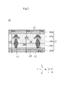
- FIG. FIG. 2 is a cross-sectional view along AA in FIG. 3 is an enlarged view of the upper major surfaces of the signal conductor layer 20 and the reference conductor layer 22.
- FIG. FIG. 4 is an enlarged view of the lower main surface of the reference conductor layer 24.
- FIG. FIG. 5 shows cross-sectional profiles of the surfaces of the reference conductor layers 22 and 24 .
- FIG. 6 is a perspective view of electronic device 100 including multilayer substrate 10 with laminated body 12 folded.
- FIG. 7 is a top view of the multilayer substrate 10 with the laminate 12 laid out flat.
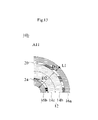
- FIG. 8 is a cross-sectional view of the first region A11.
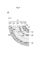
- FIG. 9 is a cross-sectional view of the second area A12.
- FIG. 10 is a cross-sectional view of the first region A11.
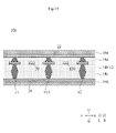
- FIG. 11 is a cross-sectional view of the second area A12.
- FIG. 12 is an exploded perspective view of the multilayer substrate 10b.
- FIG. 13 is a cross-sectional view of the first region A11.
- FIG. 14 is a top view of the multilayer substrate 10c.
- FIG. 15 is a cross-sectional view of the third area A13.
- FIG. 16 is a cross-sectional view of the fourth area A14.
- FIG. 17 is a top view of the multilayer substrate 10d.
- FIG. 18 is a top view of the multilayer substrate 10e.
- FIG. 19 is a cross-sectional view of the multilayer substrate 10e taken along the first polygonal line L1.
- FIG. 20 is a cross-sectional view of the multilayer substrate 10e along the second polygonal line L2.
- FIG. 21 is a top view of the multilayer substrate 10g.
- FIG. 1 is an exploded perspective view of a multilayer substrate 10.
- FIG. 1 only representative interlayer connection conductors v1 and v2 among the plurality of interlayer connection conductors v1 and the plurality of interlayer connection conductors v2 are denoted by reference numerals.
- FIG. 2 is a cross-sectional view along AA in FIG. 3 is an enlarged view of the upper major surfaces of the signal conductor layer 20 and the reference conductor layer 22.
- FIG. FIG. 4 is an enlarged view of the lower main surface of the reference conductor layer 24.
- FIG. 5 shows cross-sectional profiles of the surfaces of the reference conductor layers 22 and 24 .
- FIG. 6 is a perspective view of electronic device 100 including multilayer substrate 10 with laminated body 12 folded.
- FIG. 7 is a top view of the multilayer substrate 10 with the laminate 12 laid out flat.
- FIG. 8 is a cross-sectional view of the first region A11.
- FIG. 9 is a cross-sectional view of the second area A12.
- a stacking direction in which the plurality of insulating layers 14a to 14c, 16a, and 16b are stacked is defined as a vertical direction.
- the horizontal direction is perpendicular to the vertical direction.
- a direction orthogonal to the left-right direction and the up-down direction is defined as the front-rear direction. Note that the vertical direction, the front-rear direction, and the left-right direction in the present embodiment do not have to match the vertical direction, the front-rear direction, and the left-right direction when the multilayer substrate 10 is used.
- X is a part or member of the multilayer substrate 10.
- each part of X is defined as follows.
- front of X is meant the front half of X.
- Back of X means the back half of X.
- the left part of X means the left half of X.
- the right part of X means the right half of X.
- Top of X means the top half of X.
- the lower part of X means the lower half of X.
- the leading edge of X means the leading edge of X.
- the trailing end of X means the trailing end of X.
- the left end of X means the end of X in the left direction.
- the right end of X means the end of X in the right direction.
- the upper end of X means the end of X in the upward direction.
- the lower end of X means the lower end of X.
- the front end of X means the front end of X and its vicinity.
- the rear end of X means the rear end of X and its vicinity.
- the left end of X means the left end of X and its vicinity.
- the right end of X means the right end of X and its vicinity.
- the upper end of X means the upper end of X and its vicinity.
- the lower end of X means the lower end of X and its vicinity.
- the multilayer substrate 10 transmits high frequency signals.
- a multilayer substrate 10 is used to electrically connect two circuits in an electronic device such as a smart phone.
- the multilayer substrate 10 includes a laminate 12, a signal conductor layer 20 (third metal foil layer), a reference conductor layer 22 (first metal foil layer), and a reference conductor layer 24 (second metal foil layer). ), a signal terminal 26, a plurality of interlayer connection conductors v1, a plurality of interlayer connection conductors v2 and an interlayer connection conductor v3.
- the laminated body 12 has a plate shape having an upper main surface (first main surface) and a lower main surface (second main surface) arranged in the vertical direction (the lamination direction of the plurality of insulator layers).
- the laminate 12 has a first section A1 to a fourth section A4.
- the first section A1 to the fourth section A4 are connected so as to line up in this order.
- the first section A1 has a strip shape extending in the left-right direction.
- the second section A2 is connected to the right end of the first section A1.
- the second section A2 has a strip shape extending rearward from the right end of the first section A1.
- the third section A3 is connected to the rear end of the second section A2.
- the third section A3 has a strip shape extending rightward from the rear end of the second section A2.
- the fourth section A4 is connected to the right end of the third section A3.
- the fourth section A4 has a rectangular shape when viewed in the vertical direction.
- the width in the front-rear direction of the fourth section A4 is greater than the width in the front-rear direction of the third section A3.
- the laminate 12 has a structure in which insulator layers 14a to 14c, 16a, and 16b (a plurality of insulator layers) are laminated in the stacking direction.
- the insulator layers 16a, 14a to 14c, 16b are arranged in this order from top to bottom.
- the insulator layers 14a to 14c have the same shape as the laminate 12 when viewed in the vertical direction.
- the material of the insulator layers 14a to 14c is thermoplastic resin.
- Thermoplastic resins are, for example, thermoplastic resins such as liquid crystal polymer and PTFE (polytetrafluoroethylene).
- the material of the insulator layers 14a-14c may be polyimide.
- the reference conductor layer 22 (first metal foil layer) is provided on the laminate 12 .
- the reference conductor layer 22 is located on the upper main surface of the insulator layer 14a.
- the reference conductor layer 22 is fixed to the upper main surface of the insulator layer 14a. Accordingly, as shown in FIG. 2, the distance D1 between the reference conductor layer 22 and the upper main surface (first main surface) of the laminate 12 is the distance between the reference conductor layer 22 (first metal foil layer) and the lower main surface ( second main surface) is shorter than the distance D2.
- the reference conductor layer 22 covers substantially the entire upper main surface of the insulator layer 14a. However, the reference conductor layer 22 is not in contact with a signal terminal 26, which will be described later.
- the reference conductor layer 24 (second metal foil layer) is provided on the laminate 12 .
- the reference conductor layer 24 is located on the lower main surface of the insulator layer 14c.
- the reference conductor layer 24 is fixed to the lower main surface of the insulator layer 14c. Accordingly, as shown in FIG. 2, the distance D4 between the reference conductor layer 24 and the lower main surface (second main surface) of the laminate 12 is the distance between the reference conductor layer 24 (second metal foil layer) and the upper main surface ( first main surface) is shorter than the distance D3.
- the reference conductor layer 24 covers substantially the entire lower main surface of the insulator layer 14c.
- the reference conductor layers 22, 24 as described above are connected to a reference potential.
- the reference potential is, for example, the ground potential.
- the signal conductor layer 20 (third metal foil layer) is provided on the laminate 12 .
- the signal conductor layer 20 is located on the upper main surface of the insulator layer 14b.
- the signal conductor layer 20 is fixed to the upper main surface of the insulator layer 14b. Accordingly, as shown in FIG. 2, the distance D5 between the signal conductor layer 20 (third metal foil layer) and the upper main surface (first main surface) of the laminate 12 is layer) and the lower main surface (second main surface) of the laminate 12 than the distance D6.
- the signal conductor layer 20 has a linear shape extending along the laminate 12 when viewed in the vertical direction.
- the signal conductor layer 20 extends in the left-right direction at the center of the first section A1 in the front-rear direction and the center of the third section A3 in the front-rear direction.
- the signal conductor layer 20 extends in the front-rear direction at the center of the second section A2 in the left-right direction.
- the right end portion of the signal conductor layer 20 is positioned at the center in the front-rear direction and the center in the left-right direction of the fourth section A4.
- the signal conductor layer 20 as described above overlaps the reference conductor layers 22 and 24 when viewed in the vertical direction. As a result, the signal conductor layer 20 and the reference conductor layers 22, 24 form a stripline structure. A high-frequency signal is transmitted to the signal conductor layer 20 as described above.
- the signal terminal 26 is provided on the laminate 12 .
- the signal terminal 26 is located on the upper major surface of the insulator layer 14a, as shown in FIG.
- the signal terminal 26 is fixed to the upper main surface of the insulator layer 14a.
- the signal terminal 26 has a rectangular shape when viewed in the vertical direction.
- the signal terminal 26 overlaps the right end portion of the signal conductor layer 20 when viewed in the vertical direction.
- the signal conductor layer 20, the reference conductor layers 22, 24, and the signal terminal 26 are formed, for example, by etching a metal foil provided on the upper main surface or the lower main surface of the insulator layers 14b, 14a, 14c. It is The metal foil is, for example, copper foil. Such metal foils are made by depositing metal on a drum. When streaky unevenness extending in one direction exists on the surface of the drum, the streaky unevenness is transferred to the metal foil formed on the drum. In the multilayer substrate 10, the direction in which streaky unevenness (hereinafter referred to as streak) extends is specified. In other words, the surface of the metal foil of the multilayer substrate 10 is provided with unevenness extending in one direction. A streak in this specification is a linear depression extending in one direction.
- the width of the muscle is much smaller than the length of the muscle.
- Muscle length is the size of a muscle in one direction.
- the width of the stripe is the size of the stripe in a direction orthogonal to one direction. Sufficiently small means, for example, that the width of the stripe is 1/10 or less of the length of the stripe. Such streaks are described, for example, in JP-A-2019-143247.
- a plurality of streaks extending in the first direction DIR1 form the upper main surface of the reference conductor layer 22 (first metal foil layer) and the upper main surface of the signal terminal . provided on the face.
- the first direction DIR1 is the horizontal direction.
- a plurality of streaks are provided on the entire upper main surface of the reference conductor layer 22 (first metal foil layer) and the entire upper main surface of the signal terminal 26 .
- a plurality of streaks extending in a second direction DIR2 different from the first direction DIR1 are formed on the lower main surface of the reference conductor layer 24 (second metal foil layer).
- the second direction DIR2 is the front-rear direction.
- a plurality of streaks are provided over the entire lower main surface of the reference conductor layer 24 (second metal foil layer).
- a plurality of streaks extending in the third direction DIR3 are provided on the upper main surface of the signal conductor layer 20 (third metal foil layer) when viewed in the vertical direction (laminating direction).
- the third direction DIR3 is the horizontal direction.
- a plurality of streaks are provided over the entire upper main surface of the signal conductor layer 20 (third metal foil layer).
- multiple streaks provided on the reference conductor layers 22 and 24 can be confirmed in the following directions.
- the reference conductor layers 22 and 24 are observed with a laser microscope at a magnification of 20 times. At this time, the multiple streaks have the following sizes.
- the cross-sectional profiles of the surfaces of the reference conductor layers 22 and 24 have a structure as shown in FIG.
- the surfaces of the reference conductor layers 22 and 24 have irregularities within a range of ⁇ 1 ⁇ m with respect to the reference height.
- the interlayer connection conductor v3 electrically connects the signal conductor layer 20 and the signal terminal 26, as shown in FIG.
- the interlayer connection conductor v3 vertically penetrates the insulator layer 14a.
- the upper end of the interlayer connection conductor v3 is in contact with the signal terminal 26 .
- a lower end of the interlayer connection conductor v3 is in contact with the signal conductor layer 20 .
- a plurality of interlayer connection conductors v1 and a plurality of interlayer connection conductors v2 electrically connect the reference conductor layer 22 and the reference conductor layer 24 .
- a plurality of interlayer connection conductors v1 and a plurality of interlayer connection conductors v2 penetrate the insulator layers 14a to 14c in the vertical direction. Upper ends of the plurality of interlayer connection conductors v1 and upper ends of the plurality of interlayer connection conductors v2 are in contact with the reference conductor layer 22 . Lower ends of the plurality of interlayer connection conductors v1 and lower ends of the plurality of interlayer connection conductors v2 are in contact with the reference conductor layer 24 .
- a plurality of interlayer connection conductors v1 are arranged along the signal conductor layer 20 at regular intervals.
- a plurality of interlayer connection conductors v1 are located in front of the signal conductor layer 20 in the first section A1 and the third section A3.
- a plurality of interlayer connection conductors v1 are positioned to the right of the signal conductor layer 20 in the second section A2.
- the plurality of interlayer connection conductors v2 are arranged along the signal conductor layer 20 at regular intervals.
- a plurality of interlayer connection conductors v2 are positioned behind the signal conductor layer 20 in the first section A1 and the third section A3.
- the plurality of interlayer connection conductors v2 are positioned to the left of the signal conductor layer 20 in the second section A2.
- the plurality of interlayer connection conductors v1, the plurality of interlayer connection conductors v2, and the interlayer connection conductors v3 are formed by filling the through-holes provided in the insulating layers 14a to 14c with a conductive paste and solidifying the conductive paste by heating. It is formed.
- the insulator layer 16a is laminated on the insulator layer 14a.
- the insulator layer 16 a protects the reference conductor layer 22 by covering the reference conductor layer 22 .
- the upper main surface of the insulator layer 16 a is the upper main surface of the laminate 12 .
- openings ha to hc are provided in the fourth section A4 of the insulator layer 16a.
- the openings hb, ha, hc are arranged in this order from front to back.
- the signal terminal 26 is exposed outside from the laminate 12 through the opening ha.
- a part of the reference conductor layer 22 is exposed outside from the laminate 12 through the openings hb and hc.
- the signal terminal 26 is connected to a signal terminal of a circuit board (not shown) by soldering.
- a portion of the reference conductor layer 22 is connected to a reference terminal of a circuit board (not shown) by soldering.
- the insulator layer 16b is laminated under the insulator layer 14c.
- the insulator layer 16 b protects the reference conductor layer 24 by covering the reference conductor layer 24 .
- the lower main surface of the insulator layer 16 b is the lower main surface of the laminate 12 .
- the material of the insulator layers 16a and 16b is different from the material of the insulator layers 14a-14c.
- the insulator layers 16a and 16b may be formed by printing an insulating paste, or may be formed by attaching an insulating sheet.
- the multilayer substrate 10 as described above is used by being bent at a plurality of points, as shown in FIG. More specifically, the laminate 12 has a first area A11 and a second area A12, as shown in FIG. As shown in FIG. 8 , the first region A11 is formed in the first region A11 such that the upper main surface (first main surface) of the laminate 12 is positioned closer to the outer periphery than the lower main surface (second main surface) of the laminate 12 . It has a structure in which the laminate 12 is bent at the polygonal line L1. The first polygonal line L1 extends in the front-rear direction.
- the first polygonal line L1 is orthogonal to the left-right direction in which the first section A1 extends in the state in which the multilayer substrate 10 is unfolded.
- the term "laminate 12 is bent" means that the laminate 12 is deformed by applying an external force.
- the deformation may be plastic deformation, elastic deformation, or both plastic deformation and elastic deformation.
- the second region A12 is arranged so that the upper main surface (first main surface) of the laminate 12 is positioned radially inward from the lower main surface (second main surface) of the laminate 12 . It has a structure in which the laminate 12 is bent at the two fold lines L2.
- the second polygonal line L2 is not parallel to the first polygonal line L1, as shown in FIG. In this embodiment, the second polygonal line L2 extends in the left-right direction. Therefore, the second polygonal line L2 is perpendicular to the front-rear direction in which the second section A2 extends when the multilayer substrate 10 is unfolded.
- the distance D1 between the reference conductor layer 22 (first metal foil layer) and the upper main surface (first main surface) of the laminate 12 is is shorter than the distance D2 between the reference conductor layer 22 (first metal foil layer) and the lower main surface (second main surface) of the laminate 12 . Accordingly, in the first region A11, the reference conductor layer 22 (first metal foil layer) is located on the outer peripheral side of the center of the laminate 12 in the lamination direction. As shown in FIGS.
- the distance D4 between the reference conductor layer 24 and the lower main surface (second main surface) of the laminate 12 is shorter than the distance D3 between the second metal foil layer) and the upper main surface (first main surface). Accordingly, in the second region A12, the reference conductor layer 24 (second metal foil layer) is located on the outer peripheral side of the center of the laminate 12 in the lamination direction.
- the signal conductor layer 20 (third metal foil layer) and the upper main surface (first main surface) of the laminate 12
- the distance D5 is shorter than the distance D6 between the signal conductor layer 20 (third metal foil layer) and the lower main surface (second main surface) of the laminate 12 .
- the signal conductor layer 20 (third metal foil layer) is located on the outer peripheral side of the center of the laminate 12 in the lamination direction.
- the signal conductor layer 20 (third metal foil layer) is located on the inner peripheral side from the center of the laminate 12 in the lamination direction.
- first direction DIR1 a plurality of streaks extending in the first direction DIR1 are provided on the upper main surface of the reference conductor layer 22 (first metal foil layer) when viewed in the vertical direction (laminating direction). A plurality of streaks are provided over the entire upper main surface of the reference conductor layer 22 .
- the first direction DIR1 is the horizontal direction.
- the first polygonal line L1 extends in the front-rear direction.
- the second polygonal line L2 extends in the left-right direction. Therefore, in the state in which the laminated body 12 is laid out on a plane, the first direction DIR1 intersects the first polygonal line L1 when viewed in the vertical direction (laminating direction).
- the second direction DIR2 intersects the second polygonal line L2 when viewed in the vertical direction (laminating direction).
- the angle ⁇ 11 formed by the first direction DIR1 and the first polygonal line L1 is 90° when viewed in the vertical direction (stacking direction) in the state in which the laminated body 12 is laid out on a plane.
- the angle ⁇ 12 formed by the first direction DIR1 and the second polygonal line L2 when viewed in the vertical direction (laminating direction) is 0°.
- the angle ⁇ 11 formed by the first direction DIR1 and the first polygonal line L1 when viewed in the vertical direction (laminating direction) is the same as the angle ⁇ 11 formed by the first direction DIR1 and the second polygonal line L2.
- a line located on the upper main surface of the reference conductor layer 22 and parallel to the second polygonal line L2 is less likely to intersect with the plurality of streaks provided in the reference conductor layer 22 . Therefore, the line serving as the surface roughness measurement range is set to have a length that intersects the plurality of lines provided on the upper main surface of the reference conductor layer 22 .
- the surface roughness of the upper main surface of the reference conductor layer 22 in the direction parallel to the first polygonal line L1 is greater than the surface roughness of the upper main surface of the reference conductor layer 22 in the direction parallel to the second polygonal line L2.
- the surface roughness can be measured with, for example, a contact-type stylus profilometer or a non-contact laser microscope.
- the surface roughness is measured according to the following procedure. First, prepare the sample. The insulator layers 16a, 16b are removed to expose the reference conductor layers 22,24. The insulator layers 16a and 16b may be removed by dissolving the insulator layers 16a and 16b with a solvent, or by scraping off the insulator layers 16a and 16b.
- a plurality of streaks extending in the second direction DIR2 when viewed in the vertical direction (laminating direction) are provided on the lower main surface of the reference conductor layer 24 (second metal foil layer). A plurality of streaks are provided over the entire lower main surface of the reference conductor layer 24 .
- the second direction DIR2 is the front-rear direction.
- the first polygonal line L1 extends in the front-rear direction.
- the second polygonal line extends in the left-right direction. Therefore, in the state in which the laminated body 12 is laid out on a plane, the angle ⁇ 22 formed by the second direction DIR2 and the second polygonal line L2 when viewed in the vertical direction (laminating direction) is 90°.
- the angle ⁇ 21 formed by the second direction DIR2 and the first polygonal line L1 when viewed in the vertical direction (stacking direction) in the state in which the laminated body 12 is laid out on a plane is 0°.
- the angle ⁇ 22 formed by the second direction DIR2 and the second polygonal line L2 when viewed in the vertical direction (stacking direction) in the state in which the laminate 12 is spread out on a plane is greater than the angle ⁇ 21 formed by Thereby, the surface roughness of the lower main surface of the reference conductor layer 24 in the direction parallel to the second polygonal line L2 is greater than the surface roughness of the lower main surface of the reference conductor layer 24 in the direction parallel to the first polygonal line L1.
- the third direction DIR3 is the horizontal direction.
- the first polygonal line L1 extends in the front-rear direction.
- the second polygonal line L2 extends in the left-right direction. Therefore, in the state in which the laminated body 12 is laid out on a plane, the angle ⁇ 31 formed by the third direction DIR3 and the first polygonal line L1 when viewed in the vertical direction (laminating direction) is 90°.
- An angle ⁇ 32 formed between the third direction DIR3 and the second polygonal line L2 when viewed in the vertical direction (stacking direction) in the state in which the laminated body 12 is laid out on a plane is 0°.
- an angle ⁇ 31 formed by the third direction DIR3 and the first polygonal line L1 when viewed in the vertical direction (laminating direction) is formed by the third direction DIR3 and the second polygonal line L2. greater than the angle ⁇ 32.
- the surface roughness of the upper main surface of the signal conductor layer 20 in the direction parallel to the first polygonal line L1 is greater than the surface roughness of the upper main surface of the signal conductor layer 20 in the direction parallel to the second polygonal line L2.
- the surface roughness of the main surface of the reference conductor layer 22 (first metal foil layer) and the surface roughness of the main surface of the reference conductor layer 24 (second metal foil layer) are similar to those of the signal conductor layer 20 (third metal foil layer). layer) is smaller than the surface roughness of the main surface. More specifically, the surface roughness of the upper main surface of the reference conductor layer 22, the surface roughness of the lower main surface of the reference conductor layer 22, the surface roughness of the upper main surface of the reference conductor layer 24, and the lower surface of the reference conductor layer 24 The surface roughness of the main surface is smaller than the surface roughness of the upper main surface of the signal conductor layer 20 and the surface roughness of the upper main surface of the signal conductor layer 20 .
- the surface roughness of the upper main surface of the reference conductor layer 22 and the surface roughness of the lower main surface of the reference conductor layer 24 are smaller than the surface roughness of the upper main surface of the signal conductor layer 20 .
- Surface roughness here is the surface roughness within a square having a given size.
- the multilayer substrate 10 as described above is used as part of an electronic device 100 as shown in FIG.
- An electronic device 100 includes a multilayer substrate 10 and a housing 102 .
- the housing 102 accommodates the multilayer substrate 10 .
- the electronic device 100 is a wireless communication terminal such as a smart phone.
- the upper main surface of the reference conductor layer 22 and the lower main surface of the reference conductor layer 24 are provided with a plurality of stripes extending in one direction. If the angle formed by the polygonal line of the reference conductor layers 22 and 24 and the direction in which the plurality of streaks extend becomes smaller, the reference conductor layers 22 and 24 are more likely to break. In particular, a large tensile stress is applied to the reference conductors positioned on the outer peripheral side of the reference conductor layers 22 and 24 .
- the reference conductor The reference conductors located on the outer peripheral side of layers 22 and 24 are more susceptible to damage.
- the laminate 12 is bent in the lamination direction.
- the laminate 12 is bent at the first polygonal line L1 and the second polygonal line L2.
- the laminate 12 is bent at the first fold line L1 so that the upper main surface of the laminate 12 is positioned closer to the outer periphery than the lower main surface of the laminate 12 .
- the laminate 12 is bent at the second fold line L2 so that the upper main surface of the laminate 12 is located inside the lower main surface of the laminate 12 .
- the distance D1 between the reference conductor layer 22 and the upper main surface of the laminate 12 is shorter than the distance D2 between the reference conductor layer 22 and the lower main surface of the laminate 12 in the first region A11.
- the reference conductor layer 22 (first metal foil layer) is located on the outer peripheral side of the center of the laminate 12 in the lamination direction. Therefore, a large tensile stress is applied to the reference conductor layer 22 in the first region A11.
- the distance D4 between the reference conductor layer 24 and the lower main surface of the laminate 12 is shorter than the distance D3 between the reference conductor layer 24 and the upper main surface of the laminate 12.
- the reference conductor layer 24 (second metal foil layer) is located on the outer peripheral side of the center of the laminate 12 in the lamination direction. Therefore, a large tensile stress is applied to the reference conductor layer 24 in the second region A12.
- the angle ⁇ 11 formed by the first direction DIR1 and the first polygonal line L1 when viewed in the vertical direction is the angle ⁇ 12 formed by the first direction DIR1 and the second polygonal line L2. greater than Accordingly, even if a large tensile stress is applied to the reference conductor layer 22 in the first region A11, damage to the reference conductor layer 22 is suppressed.
- the angle ⁇ 22 formed by the second direction DIR2 and the second polygonal line L2 when viewed in the vertical direction is the angle formed by the second direction DIR2 and the first polygonal line L1. larger than ⁇ 21.
- the confirmation of the first direction DIR1, the confirmation of the second direction DIR2, the measurement of the surface roughness of the upper main surface of the reference conductor layer 22, and the measurement of the surface roughness of the lower main surface of the reference conductor layer 24 are performed by, for example, an insulating This is done by dissolving and removing the body layers 16a and 16b with a solvent.
- the distance D5 between the signal conductor layer 20 and the upper main surface of the laminate 12 is shorter than the distance D6 between the signal conductor layer 20 and the lower main surface of the laminate 12 in the first region A11.
- the signal conductor layer 20 (the third metal foil layer) is located on the outer peripheral side of the center of the laminate 12 in the lamination direction. Therefore, a large tensile stress is applied to the signal conductor layer 20 in the first region A11. In particular, since the signal conductor layer 20 has a narrow line width, disconnection is likely to occur.
- the angle ⁇ 31 formed by the third direction DIR3 and the first polygonal line L1 when viewed in the vertical direction is the angle ⁇ 32 formed by the third direction DIR3 and the second polygonal line L2. greater than As a result, even if a large tensile stress is applied to the signal conductor layer 20 in the first region A11, damage to the signal conductor layer 20 having a narrow line width is effectively suppressed.
- the surface roughness of the main surface of the reference conductor layer 22 (first metal foil layer) and the surface roughness of the main surface of the reference conductor layer 24 (second metal foil layer) are similar to those of the signal conductor layer 20 (third metal foil layer). layer) is smaller than the surface roughness of the main surface.
- the surface roughness of the upper main surface of the reference conductor layer 22 and the surface roughness of the lower main surface of the reference conductor layer 24 are smaller than the surface roughness of the upper main surface of the signal conductor layer 20 .
- the reference conductor layers 22 and 24 are less likely to be damaged when the multilayer substrate 10 is bent.
- the material of the insulator layers 14a to 14c is thermoplastic resin. Therefore, it is easy to plastically deform the laminate 12 .
- FIG. 10 is a cross-sectional view of the first region A11.
- FIG. 11 is a cross-sectional view of the second area A12.
- the multilayer substrate 10a differs from the multilayer substrate 10 in the position of the signal conductor layer 20 and in the third direction DIR3 in which the plurality of stripes provided on the lower main surface of the signal conductor layer 20 extend. More specifically, the signal conductor layer 20 is located on the lower major surface of the insulator layer 14b. The signal conductor layer 20 is fixed to the lower main surface of the insulator layer 14b. Accordingly, in the first region A11 and the second region A12, the distance D6 between the signal conductor layer 20 (third metal foil layer) and the lower main surface (second main surface) of the laminate 12 is the same as the signal conductor layer 20 ( (third metal foil layer) and the upper main surface (first main surface) of the laminate 12 (the first main surface) is shorter than the distance D5.
- the signal conductor layer 20 (third metal foil layer) is located inside the center of the laminate 12 in the lamination direction.
- the signal conductor layer 20 is located on the outer peripheral side of the center of the laminate 12 in the lamination direction.
- the third direction DIR3 is the front-rear direction. Then, in the state in which the laminated body 12 is unfolded on a plane, the angle ⁇ 32 formed by the third direction DIR3 and the second polygonal line L2 when viewed in the vertical direction (laminating direction) is such that the third direction DIR3 forms an angle ⁇ 32 with the first polygonal line L1. is greater than the forming angle ⁇ 31.
- the surface roughness of the lower main surface of the signal conductor layer 20 in the direction parallel to the second polygonal line L2 is greater than the surface roughness of the lower main surface of the signal conductor layer 20 in the direction parallel to the first polygonal line L1.
- the rest of the structure of the multilayer substrate 10a is the same as that of the multilayer substrate 10, so description thereof will be omitted.
- the multi-layer board 10a can have the same effect as the multi-layer board 10. FIG.
- the distance D6 between the signal conductor layer 20 and the lower main surface of the laminate 12 is shorter than the distance D5 between the signal conductor layer 20 and the upper main surface of the laminate 12 in the second region A12.
- the signal conductor layer 20 is located on the outer peripheral side of the center of the laminate 12 in the lamination direction. Therefore, a large tensile stress is applied to the signal conductor layer 20 in the second region A12.
- the angle ⁇ 32 formed by the third direction DIR3 and the second polygonal line L2 when viewed in the vertical direction is the angle ⁇ 31 formed by the third direction DIR3 and the first polygonal line L1. greater than As a result, even if a large tensile stress is applied to the signal conductor layer 20, damage to the signal conductor layer 20 is suppressed.
- FIG. 12 is an exploded perspective view of the multilayer substrate 10b.
- FIG. 13 is a cross-sectional view of the first region A11.
- FIG. 7 is referred to as a top view of the multilayer substrate 10b with the laminate 12 unfolded on the plane.
- the multilayer substrate 10b differs from the multilayer substrate 10 in that a portion of the insulator layer 14a is missing. More specifically, the insulator layer 14a and the reference conductor layer 22 are absent in a portion of the first section A1.
- the first polygonal line L1 and the first area A11 are located in a portion where the insulator layer 14a and the reference conductor layer 22 do not exist in the first section A1.
- the distance D1 between the signal conductor layer 20 (first metal foil layer) and the upper main surface (first main surface) of the laminate 12 is the same as the signal conductor layer 20 (first metal foil layer). shorter than the distance D2 to the lower main surface (second main surface) of the body 12;
- the signal conductor layer 20 (first metal foil layer) is located on the outer peripheral side from the center of the stack 12 in the stacking direction.
- a plurality of streaks extending in the first direction DIR1 when viewed in the vertical direction (laminating direction) are provided on the upper main surface of the signal conductor layer 20 (first metal foil layer).
- a plurality of streaks are provided over the entire upper main surface of the signal conductor layer 20 .
- the first direction DIR1 is the horizontal direction.
- the angle ⁇ 11 formed by the first direction DIR1 and the first polygonal line L1 when viewed in the vertical direction (laminating direction) is the same as the angle ⁇ 11 formed by the first direction DIR1 and the second polygonal line L2. greater than the forming angle ⁇ 12.
- the surface roughness of the upper main surface of the signal conductor layer 20 in the direction parallel to the first polygonal line L1 is greater than the surface roughness of the upper main surface of the signal conductor layer 20 in the direction parallel to the second polygonal line L2.
- the rest of the structure of the multilayer substrate 10b is the same as that of the multilayer substrate 10, so the description is omitted. Since the multilayer substrate 10b is the same as the multilayer substrate 10, the description thereof is omitted.
- the distance D1 between the signal conductor layer 20 and the upper main surface of the laminate 12 is shorter than the distance D2 between the signal conductor layer 20 and the lower main surface of the laminate 12 in the first region A11.
- the signal conductor layer 20 first metal foil layer
- the signal conductor layer 20 is located on the outer peripheral side from the center of the stack 12 in the stacking direction. Therefore, a large tensile stress is applied to the signal conductor layer 20 in the first region A11.
- the angle ⁇ 11 formed by the first direction DIR1 and the first polygonal line L1 when viewed in the vertical direction is the angle ⁇ 12 formed by the first direction DIR1 and the second polygonal line L2. greater than As a result, even if a large tensile stress is applied to the signal conductor layer 20, damage to the signal conductor layer 20 is suppressed.
- the thickness of the laminate 12 in the vertical direction (laminating direction) in the first region A11 is (Lamination direction) is smaller than the thickness. Therefore, it becomes easy to bend the laminate 12 in the first region A11.
- a plurality of streaks extending in the fifth direction DIR5 are provided on the upper main surface of the reference conductor layer 22 when viewed in the vertical direction (stacking direction). A plurality of streaks are provided over the entire upper main surface of the reference conductor layer 22 .
- the fifth direction DIR5 is the front-rear direction. This suppresses damage to the reference conductor layer 22 in the second region A12. In this way, since the reference conductor layer 22 is not provided in the first region A11, the fifth direction DIR5 in which the plurality of streaks provided in the reference conductor layer 22 extend extends from the reference conductor layer 22 in the second polygonal line L2. It is set in the direction in which the occurrence of breakage is suppressed.
- FIG. 14 is a top view of the multilayer substrate 10c.
- FIG. 15 is a cross-sectional view of the third area A13.
- FIG. 16 is a cross-sectional view of the fourth area A14.
- the multilayer board 10c differs from the multilayer board 10 in that it is bent at the first polygonal line L1, the second polygonal line L2, the third polygonal line L3, and the fourth polygonal line L4. More specifically, the laminate 12 has a third area A13 and a fourth area A14. In the third region A13, the laminate 12 is positioned along the third fold line L3 such that the lower main surface (second main surface) of the laminate 12 is located on the outer peripheral side of the upper main surface (first main surface) of the laminate 12. It has a bendable structure.
- the third polygonal line L3 and the third area A13 are located in the first section A1.
- the third polygonal line L3 extends in the front-rear direction.
- the radius of curvature of the third area A13 is larger than the radius of curvature of the first area A11. That is, the third area A13 is more gently bent than the first area A11. Also, the radius of curvature of the third region A13 is larger than the radius of curvature of the second region A12. That is, the third area A13 is more gently bent than the second area A12.
- the laminate 12 is positioned along the fourth fold line L4 such that the upper main surface (first main surface) of the laminate 12 is located on the outer peripheral side of the lower main surface (second main surface) of the laminate 12. It has a bendable structure.
- the fourth polygonal line L4 and the fourth area A14 are located in the second section A2.
- the fourth polygonal line L4 extends in the left-right direction.
- the radius of curvature of the fourth area A14 is greater than the radius of curvature of the second area A12. That is, the fourth area A14 is more moderately bent than the second area A12.
- the radius of curvature of the fourth area A14 is greater than the radius of curvature of the first area A11. That is, the fourth area A14 is more gently bent than the first area A11.
- the distance D4 between the reference conductor layer 24 (second metal foil layer) and the lower main surface (second main surface) of the laminate 12 is equal to that of the reference conductor layer 24 (second metal foil layer). and the upper main surface (first main surface) of the laminate 12 than the distance D3.
- the reference conductor layer 24 (second metal foil layer) is located on the outer peripheral side of the center of the laminate 12 in the lamination direction.
- the distance D1 between the reference conductor layer 22 (first metal foil layer) and the upper main surface (first main surface) of the laminate 12 is the same as the reference conductor layer 22 (first metal foil layer). shorter than the distance D2 to the lower main surface (second main surface) of the body 12; In the fourth area A14, the reference conductor layer 22 (first metal foil layer) is located on the outer peripheral side of the center of the laminate 12 in the lamination direction.
- a plurality of stripes extending in the first direction DIR ⁇ b>1 when viewed in the vertical direction (laminating direction) are provided on the upper main surface of the reference conductor layer 22 (first metal foil layer) and the upper main surface of the signal terminal 26 .
- a plurality of streaks are provided on the entire upper main surface of the reference conductor layer 22 and the entire upper main surface of the signal terminal 26 .
- the first direction DIR1 is the horizontal direction.
- a plurality of streaks extending in the second direction DIR2 when viewed in the vertical direction (laminating direction) are provided on the lower main surface of the reference conductor layer 24 (second metal foil layer).
- a plurality of streaks are provided over the entire lower main surface of the reference conductor layer 24 .
- the second direction DIR2 is the front-rear direction. Therefore, when the laminate 12 is laid out on a plane, the angle ⁇ 23 formed by the second direction DIR2 and the third polygonal line L3 when viewed in the vertical direction (laminating direction) is less than the forming angle ⁇ 22. Thereby, the surface roughness of the lower main surface of the reference conductor layer 24 in the direction parallel to the third polygonal line L3 is smaller than the surface roughness of the lower main surface of the reference conductor layer 24 in the direction parallel to the second polygonal line L2.
- the first direction DIR1 forms an angle ⁇ 14 with the fourth polygonal line L4 when viewed in the vertical direction (laminating direction). smaller than the angle ⁇ 11.
- the surface roughness of the upper main surface of the reference conductor layer 22 in the direction parallel to the fourth polygonal line L4 is smaller than the surface roughness of the upper main surface of the reference conductor layer 22 in the direction parallel to the first polygonal line L1.
- the rest of the structure of the multilayer substrate 10c is the same as that of the multilayer substrate 10, so description thereof will be omitted.
- the distance D4 between the reference conductor layer 24 (second metal foil layer) and the lower main surface (second main surface) of the laminate 12 is equal to the reference conductor layer 24 (second metal foil layer). foil layer) and the upper main surface (first main surface) of the laminate 12 than the distance D3.
- the reference conductor layer 24 (second metal foil layer) is located on the outer peripheral side of the center of the laminate 12 in the lamination direction. Therefore, a large tensile stress is applied to the reference conductor layer 24 in the third region A13.
- a plurality of streaks extending in the second direction DIR2 when viewed in the vertical direction (laminating direction) are provided on the lower main surface of the reference conductor layer 24 (second metal foil layer). A plurality of streaks are provided over the entire lower main surface of the reference conductor layer 24 .
- the second direction DIR2 is the front-rear direction.
- the second polygonal line L2 extends in the left-right direction.
- the third polygonal line L3 extends in the front-rear direction. Therefore, in the state in which the laminated body 12 is laid out on a plane, the angle ⁇ 23 formed by the second direction DIR2 and the third polygonal line L3 when viewed in the vertical direction (laminating direction) is less than the forming angle ⁇ 22.
- the reference conductor layer 24 may be damaged in the third area A13. Therefore, in the multilayer substrate 10c, the radius of curvature of the third region A13 is larger than the radius of curvature of the first region A11. Also, the radius of curvature of the third region A13 is larger than the radius of curvature of the second region A12. This reduces the tensile stress applied to the reference conductor layer 24 in the third region A13. As a result, according to the multilayer substrate 10c, damage to the reference conductor layer 24 can be suppressed. Similarly, in the multilayer substrate 10c, the radius of curvature of the fourth region A14 is larger than the radius of curvature of the second region A12.
- the radius of curvature of the fourth area A14 is larger than the radius of curvature of the first area A11. This reduces the tensile stress applied to the reference conductor layer 22 in the fourth region A14. As a result, according to the multilayer substrate 10c, damage to the reference conductor layer 22 can be suppressed.
- FIG. 17 is a top view of the multilayer substrate 10d.
- the multilayer board 10d differs from the multilayer board 10 in the direction in which the first polygonal line L1 extends and the direction in which the second polygonal line L2 extends. More specifically, the first polygonal line L1 is inclined clockwise with respect to the front-rear direction. The second polygonal line L2 is inclined counterclockwise with respect to the horizontal direction. However, when the laminate 12 is unfolded on a plane, the angle ⁇ 11 formed by the first direction DIR1 and the first polygonal line L1 when viewed in the vertical direction (stacking direction) is such that the first direction DIR1 and the second polygonal line L2 form an angle ⁇ 11. greater than the forming angle ⁇ 12.
- the surface roughness of the upper main surface of the reference conductor layer 22 in the direction parallel to the first polygonal line L1 is greater than the surface roughness of the upper main surface of the reference conductor layer 22 in the direction parallel to the second polygonal line L2.
- the angle ⁇ 22 formed by the second direction DIR2 and the second polygonal line L2 is the angle ⁇ 22 formed by the second direction DIR2 and the first polygonal line L1. greater than the angle ⁇ 21.
- the surface roughness of the lower main surface of the reference conductor layer 24 in the direction parallel to the second polygonal line L2 is greater than the surface roughness of the lower main surface of the reference conductor layer 24 in the direction parallel to the first polygonal line L1.
- the rest of the structure of the multilayer substrate 10d is the same as that of the multilayer substrate 10, so description thereof will be omitted.
- the multi-layer substrate 10d can have the same effect as the multi-layer substrate 10.
- FIG. 18 is a top view of the multilayer substrate 10e.
- FIG. 19 is a cross-sectional view of the multilayer substrate 10e taken along the first polygonal line L1.
- FIG. 20 is a cross-sectional view of the multilayer substrate 10e along the second polygonal line L2.
- the multilayer board 10e differs from the multilayer board 10 in that it further includes a signal conductor layer 120 and a plurality of interlayer connection conductors v11.
- the signal conductor layer 120 is provided on the laminate 12 .
- the signal conductor layer 120 is located on the upper major surface of the insulator layer 14b.
- the signal conductor layer 120 is fixed to the upper major surface of the insulator layer 14b.
- Signal conductor layer 120 is parallel to signal conductor layer 20 .
- the signal conductor layer 120 is located behind the signal conductor layer 20 in the first section A1.
- the signal conductor layer 120 is positioned to the left of the signal conductor layer 20 in the second section A2.
- the signal conductor layer 120 is positioned behind the signal conductor layer 20 in the third section A3.
- a plurality of interlayer connection conductors v11 electrically connect the reference conductor layer 22 and the reference conductor layer 24 .
- a plurality of interlayer connection conductors v11 penetrate the insulator layers 14a to 14c in the vertical direction. Upper ends of the plurality of interlayer connection conductors v11 are in contact with the reference conductor layer 22 . Lower ends of the plurality of interlayer connection conductors v11 are in contact with the reference conductor layer 24 .
- a plurality of interlayer connection conductors v11 are arranged along the signal conductor layers 20 and 120 at regular intervals.
- the plurality of interlayer connection conductors v11 are positioned between the signal conductor layer 20 and the signal conductor layer 120 when viewed in the vertical direction.
- the width of the multilayer board 10e in the front-rear direction at the first polygonal line L1 is larger than the width of the multilayer board 10e in the left-right direction at the second polygonal line L2. Therefore, the distance between the signal conductor layer 20 and the interlayer connection conductors v1 and v11 on the first polygonal line L1 can be arranged to be longer than the distance between the signal conductor layer 20 and the interlayer connection conductors v1 and v11 on the second polygonal line L2. be.
- the capacitance formed between the signal conductor layer 20 and the interlayer connection conductors v1 and v11 on the first polygonal line L1 is formed between the signal conductor layer 20 and the interlayer connection conductors v1 and v11 on the second polygonal line L2. smaller than the capacity used. Therefore, the width of the signal conductor layers 20 and 120 in the front-rear direction along the first polygonal line L1 is greater than the width of the signal conductor layers 20 and 120 in the horizontal direction along the second polygonal line L2. As a result, fluctuations in capacitance occurring in the signal conductor layer 20 are suppressed, and fluctuations in characteristic impedance occurring in the signal conductor layer 20 are suppressed.
- the rest of the structure of the multilayer substrate 10e is the same as that of the multilayer substrate 10, so the description is omitted.
- the multilayer substrate 10 e has the same effect as the multilayer substrate 10 .
- the multilayer substrate 10f differs from the multilayer substrate 10 in that it includes signal conductor layers 20 and 20a.
- the signal conductor layer 20 (third metal foil layer) is provided in the first section A1. That is, the signal conductor layer 20 (third metal foil layer) is provided in the first region A11.
- the signal conductor layer 20 is located on the upper main surface of the insulator layer 14b.
- the signal conductor layer 20 a (fourth metal foil layer) is provided on the laminate 12 .
- the signal conductor layer 20a is provided in the second section A2, the third section A3 and the fourth section A4. That is, the signal conductor layer 20a is provided in the second region A12.
- the signal conductor layer 20a is located on the lower main surface of the insulator layer 14b.
- the signal conductor layer 20a is fixed to the lower main surface of the insulator layer 14b.
- the distance D6 between the signal conductor layer 20a (fourth metal foil layer) and the lower main surface (second main surface) of the laminate 12 is the same as the signal conductor layer 20a (fourth metal foil layer).
- the signal conductor layer 20a (fourth metal foil layer) is located on the outer peripheral side of the center of the laminate 12 in the lamination direction.
- the signal conductor layer 20 and the signal conductor layer 20a are connected by an interlayer connection conductor at the boundary between the first section A1 and the second section A2.
- a plurality of stripes extending in the fourth direction DIR4 when viewed in the vertical direction (laminating direction) are provided on the lower main surface of the signal conductor layer 20a (fourth metal foil layer). A plurality of streaks are provided over the entire lower main surface of the signal conductor layer 20a.
- the fourth direction DIR4 is the front-rear direction.
- the surface roughness of the lower main surface of the signal conductor layer 20a in the direction parallel to the second polygonal line L2 is greater than the surface roughness of the lower main surface of the signal conductor layer 20a in the direction parallel to the first polygonal line L1.
- the rest of the structure of the multilayer substrate 10f is the same as that of the multilayer substrate 10, so description thereof will be omitted.
- the multi-layer board 10f can have the same effect as the multi-layer board 10. FIG.
- the distance D6 between the signal conductor layer 20a and the lower main surface of the laminate 12 is shorter than the distance D5 between the signal conductor layer 20a and the upper main surface of the laminate 12 in the second region A12.
- the signal conductor layer 20a (fourth metal foil layer) is located on the outer peripheral side of the center of the laminate 12 in the lamination direction. Therefore, a large tensile stress is applied to the signal conductor layer 20a in the second region A12.
- the angle ⁇ 42 formed by the fourth direction DIR4 and the second polygonal line L2 when viewed in the vertical direction (laminating direction) is greater than the forming angle ⁇ 41.
- FIG. 21 is a top view of the multilayer substrate 10g.
- the multilayer substrate 10g differs from the multilayer substrate 10c at the position of the fourth polygonal line L4. More specifically, the fourth polygonal line L4 is located in the third section A3. The rest of the structure of the multilayer substrate 10g is the same as that of the multilayer substrate 10c, so the description is omitted.
- the multilayer substrate 10g can have the same effect as the multilayer substrate 10c.
- the multilayer substrate according to the present invention is not limited to the multilayer substrates 10, 10a to 10g, and can be modified within the scope of the gist thereof.
- the configurations of the multilayer substrates 10, 10a to 10g may be combined arbitrarily.
- signal conductor layers 20, 20a, 120 are not essential constituents of the multilayer substrates 10, 10a to 10g.
- the thickness in the stacking direction of the laminate 12 in the second area A12 may be smaller than the thickness in the stacking direction of the laminate 12 in at least a part of the area excluding the first area A11 and the second area A12. good. Further, the thickness of the laminate 12 in the stacking direction in the first area A11 and the thickness in the stacking direction of the laminate 12 in the second area A12 are the same as the thickness of the laminate 12 in at least a part of the area excluding the first area A11 and the second area A12. may be smaller than the thickness in the stacking direction of
- the multilayer substrates 10, 10a to 10g may not have a band shape when viewed in the vertical direction.
- the multilayer substrates 10, 10a to 10g may have, for example, a rectangular shape when viewed in the vertical direction.
- the plurality of streaks may be provided on the lower main surface of the reference conductor layer 22 .
- a plurality of streaks may be provided on the upper main surface of the reference conductor layer 24 .
- the insulator layers 16a and 16b are not essential constituent elements in the multilayer substrates 10 and 10a to 10g.
- An insulator layer of the same material as that of the insulator layer 14a may be laminated on the insulator layer 14a.
- the angle ⁇ 31 formed by the third direction DIR3 and the first polygonal line L1 when viewed in the vertical direction with the laminate 12 unfolded on a plane is an angle ⁇ 31 between the third direction DIR3 and the second polygonal line L2. may be less than or equal to the angle ⁇ 32.
- the angle ⁇ 32 formed by the third direction DIR3 and the second polygonal line L2 when viewed in the vertical direction with the laminate 12 unfolded on a plane is the same as the angle ⁇ 32 formed by the third direction DIR3 and the first polygonal line L1. may be less than or equal to the angle ⁇ 31.
- the angle ⁇ 42 formed by the fourth direction DIR4 and the second polygonal line L2 when viewed in the vertical direction with the laminate 12 unfolded on a plane is the same as the angle ⁇ 42 formed by the fourth direction DIR4 and the first polygonal line L1. may be less than or equal to the angle ⁇ 41.
- the signal conductor layers 20, 20a, 120 of the multilayer substrates 10, 10a to 10g may be power conductor layers to which a power supply voltage is applied, reference conductor layers to which a reference potential is connected, or the like.
- the reference conductor layers 22, 24 of the multilayer substrates 10, 10a to 10g may be power conductor layers to which power supply voltage is applied, signal conductor layers to which high-frequency signals are transmitted, or the like.
- a metal foil formed by rolling a metal may be used to form the signal conductor layers 20, 20a, 120 and the reference conductor layers 22, 24.
- a metal foil formed by rolling also has a plurality of streaks. Streaks formed in a metal foil formed by rolling are described, for example, in Japanese Unexamined Patent Application Publication No. 2010-227971.
- the material of the insulator layers 14a to 14c may be resin other than thermoplastic resin.
- interlayer connection conductors v1 to v3 and v11 may be through-hole conductors having a structure in which conductors are formed by plating on the inner peripheral surfaces of the through holes in which the insulator layers 14a to 14c are formed.
- the fifth direction DIR5 may be a direction other than the front-rear direction.
- the fifth direction DIR5 may be, for example, the horizontal direction.
- an angle refers to an acute angle among obtuse angles and acute angles formed by the intersection of two lines.
- the radius of curvature of the third region A13 is larger than the radius of curvature of the first region A11
- the radius of curvature of the third region A13 is larger than the radius of curvature of the second region A12.
- ⁇ the radius of curvature of the fourth region A14 is greater than that of the second region A12''; and ⁇ the radius of curvature of the fourth region A14 is greater than the radius of curvature of the first region A11''. at least one of is satisfied.
- the radius of curvature of the third region A13 is greater than the radius of curvature of the first region A11
- the radius of curvature of the fourth region A14 is greater than the radius of curvature of the first region A11
- the radius of curvature of the third region A13 is greater than the radius of curvature of the second region A12
- the radius of curvature of the fourth region A14 is greater than the radius of curvature of the first region A11" are satisfied. preferably.
- the surface roughness of the main surface of the reference conductor layer 22 (first metal foil layer) and the surface roughness of the main surface of the reference conductor layer 24 (second metal foil layer) are the same as those of the signal conductor layer 20. It may be larger than the surface roughness of the main surface of the (third metal foil layer). More specifically, the surface roughness of the upper main surface of the reference conductor layer 22, the surface roughness of the lower main surface of the reference conductor layer 22, the surface roughness of the upper main surface of the reference conductor layer 24, and the lower surface of the reference conductor layer 24 The surface roughness of the main surface is larger than the surface roughness of the upper main surface of the signal conductor layer 20 and the surface roughness of the upper main surface of the signal conductor layer 20 .
- the lower main surface of the reference conductor layer 22 is in contact with the insulator layer 14a, and the upper main surface of the reference conductor layer 24 is in contact with the insulator layer 14c. Therefore, the surface roughness of the lower main surface of the reference conductor layer 22 and the surface roughness of the upper main surface of the reference conductor layer 24 are the same as the surface roughness of the upper main surface of the signal conductor layer 20 and the upper main surface of the signal conductor layer 20 . greater than the surface roughness of This makes it difficult for the reference conductor layer 22 to separate from the insulator layer 14a. Similarly, the reference conductor layer 24 is less likely to peel off from the insulator layer 14c.
- the upper main surface of the reference conductor layer 22 may be in contact with the insulator layer, and the lower main surface of the reference conductor layer 24 may be in contact with the insulator layer.
- the surface roughness of the upper main surface of the reference conductor layer 22 and the surface roughness of the lower main surface of the reference conductor layer 24 are equal to the surface roughness of the upper main surface of the signal conductor layer 20 and the surface roughness of the upper main surface of the signal conductor layer 20 . It may be greater than the surface roughness of the surface.
Landscapes
- Engineering & Computer Science (AREA)
- Microelectronics & Electronic Packaging (AREA)
- Physics & Mathematics (AREA)
- Electromagnetism (AREA)
- Manufacturing & Machinery (AREA)
- Production Of Multi-Layered Print Wiring Board (AREA)
- Structure Of Printed Boards (AREA)
- Manufacturing Of Printed Wiring (AREA)
Priority Applications (3)
| Application Number | Priority Date | Filing Date | Title |
|---|---|---|---|
| CN202290000492.2U CN221306164U (zh) | 2021-06-28 | 2022-06-20 | 多层基板以及电子设备 |
| JP2023531811A JP7380953B2 (ja) | 2021-06-28 | 2022-06-20 | 多層基板及び電子機器 |
| US18/371,591 US12424720B2 (en) | 2021-06-28 | 2023-09-22 | Multilayer substrate and electronic device |
Applications Claiming Priority (2)
| Application Number | Priority Date | Filing Date | Title |
|---|---|---|---|
| JP2021106440 | 2021-06-28 | ||
| JP2021-106440 | 2021-06-28 |
Related Child Applications (1)
| Application Number | Title | Priority Date | Filing Date |
|---|---|---|---|
| US18/371,591 Continuation US12424720B2 (en) | 2021-06-28 | 2023-09-22 | Multilayer substrate and electronic device |
Publications (1)
| Publication Number | Publication Date |
|---|---|
| WO2023276743A1 true WO2023276743A1 (ja) | 2023-01-05 |
Family
ID=84691717
Family Applications (1)
| Application Number | Title | Priority Date | Filing Date |
|---|---|---|---|
| PCT/JP2022/024462 Ceased WO2023276743A1 (ja) | 2021-06-28 | 2022-06-20 | 多層基板及び電子機器 |
Country Status (4)
| Country | Link |
|---|---|
| US (1) | US12424720B2 (https=) |
| JP (1) | JP7380953B2 (https=) |
| CN (1) | CN221306164U (https=) |
| WO (1) | WO2023276743A1 (https=) |
Families Citing this family (1)
| Publication number | Priority date | Publication date | Assignee | Title |
|---|---|---|---|---|
| WO2022209843A1 (ja) * | 2021-03-30 | 2022-10-06 | 株式会社オートネットワーク技術研究所 | 通信器及び通信装置 |
Citations (3)
| Publication number | Priority date | Publication date | Assignee | Title |
|---|---|---|---|---|
| JPH0555746A (ja) * | 1991-08-29 | 1993-03-05 | Hitachi Chem Co Ltd | 高周波用銅張り積層板及びプリント配線板 |
| WO2014065172A1 (ja) * | 2012-10-26 | 2014-05-01 | 株式会社村田製作所 | フレキシブル基板 |
| WO2019194142A1 (ja) * | 2018-04-05 | 2019-10-10 | 株式会社村田製作所 | 樹脂多層基板の製造方法および製造装置 |
Family Cites Families (6)
| Publication number | Priority date | Publication date | Assignee | Title |
|---|---|---|---|---|
| US5334800A (en) * | 1993-07-21 | 1994-08-02 | Parlex Corporation | Flexible shielded circuit board |
| JP2006005134A (ja) | 2004-06-17 | 2006-01-05 | Fujikura Ltd | フレキシブルプリント配線板及びその製造方法 |
| JP4972115B2 (ja) | 2009-03-27 | 2012-07-11 | Jx日鉱日石金属株式会社 | 圧延銅箔 |
| JP5355478B2 (ja) * | 2010-04-07 | 2013-11-27 | 株式会社フジクラ | フレキシブルプリント基板及びその製造方法 |
| JP6149016B2 (ja) | 2014-05-09 | 2017-06-14 | Jx金属株式会社 | キャリア付銅箔、銅張積層板の製造方法、電子機器の製造方法、キャリア付銅箔の製造方法、及び、プリント配線板の製造方法 |
| JP6362444B2 (ja) * | 2014-06-16 | 2018-07-25 | 日本メクトロン株式会社 | フレキシブルプリント基板およびフレキシブルプリント基板の製造方法 |
-
2022
- 2022-06-20 JP JP2023531811A patent/JP7380953B2/ja active Active
- 2022-06-20 CN CN202290000492.2U patent/CN221306164U/zh active Active
- 2022-06-20 WO PCT/JP2022/024462 patent/WO2023276743A1/ja not_active Ceased
-
2023
- 2023-09-22 US US18/371,591 patent/US12424720B2/en active Active
Patent Citations (3)
| Publication number | Priority date | Publication date | Assignee | Title |
|---|---|---|---|---|
| JPH0555746A (ja) * | 1991-08-29 | 1993-03-05 | Hitachi Chem Co Ltd | 高周波用銅張り積層板及びプリント配線板 |
| WO2014065172A1 (ja) * | 2012-10-26 | 2014-05-01 | 株式会社村田製作所 | フレキシブル基板 |
| WO2019194142A1 (ja) * | 2018-04-05 | 2019-10-10 | 株式会社村田製作所 | 樹脂多層基板の製造方法および製造装置 |
Also Published As
| Publication number | Publication date |
|---|---|
| JP7380953B2 (ja) | 2023-11-15 |
| CN221306164U (zh) | 2024-07-09 |
| US12424720B2 (en) | 2025-09-23 |
| US20240014536A1 (en) | 2024-01-11 |
| JPWO2023276743A1 (https=) | 2023-01-05 |
Similar Documents
| Publication | Publication Date | Title |
|---|---|---|
| US9113560B2 (en) | Signal line and circuit substrate | |
| JP5999239B2 (ja) | 信号伝送部品および電子機器 | |
| JP6732723B2 (ja) | 高周波伝送用プリント配線板 | |
| WO2019131286A1 (ja) | 多層基板および伝送線路装置 | |
| CN204559998U (zh) | 柔性基板及电子设备 | |
| JP4985894B2 (ja) | 信号線路 | |
| US10225928B2 (en) | Flexible board and electronic device | |
| US8648668B2 (en) | Electrical impedance precision control of signal transmission line for circuit board | |
| JPWO2010131523A1 (ja) | 信号線路及び回路基板 | |
| WO2020130010A1 (ja) | 伝送線路部材 | |
| CN104221478B (zh) | 扁平电缆 | |
| JP5445011B2 (ja) | 回路基板 | |
| CN204333194U (zh) | 高频信号线路 | |
| CN207560432U (zh) | 多层基板 | |
| WO2023276743A1 (ja) | 多層基板及び電子機器 | |
| JP7001154B2 (ja) | 伝送線路及びその実装構造 | |
| CN105682341B (zh) | 软硬结合板及移动终端 | |
| CN219979788U (zh) | 多层基板和电子设备 | |
| JP7276225B2 (ja) | センサユニット | |
| WO2023085177A1 (ja) | 多層基板 | |
| WO2017199824A1 (ja) | 多層基板、および、電子機器 | |
| CN211828497U (zh) | 树脂多层基板以及电子设备 | |
| JP2014175829A (ja) | 伝送線路、アンテナ装置及び伝送線路製造方法 | |
| WO2026048711A1 (ja) | グラウンデッドコプレーナ導波路及び電子機器 | |
| CN120711602A (zh) | 折叠式电路板及其制造方法 |
Legal Events
| Date | Code | Title | Description |
|---|---|---|---|
| 121 | Ep: the epo has been informed by wipo that ep was designated in this application |
Ref document number: 22832893 Country of ref document: EP Kind code of ref document: A1 |
|
| WWE | Wipo information: entry into national phase |
Ref document number: 2023531811 Country of ref document: JP |
|
| WWE | Wipo information: entry into national phase |
Ref document number: 202290000492.2 Country of ref document: CN |
|
| NENP | Non-entry into the national phase |
Ref country code: DE |
|
| 122 | Ep: pct application non-entry in european phase |
Ref document number: 22832893 Country of ref document: EP Kind code of ref document: A1 |