WO2023276491A1 - 過電流保護回路、半導体装置 - Google Patents
過電流保護回路、半導体装置 Download PDFInfo
- Publication number
- WO2023276491A1 WO2023276491A1 PCT/JP2022/021091 JP2022021091W WO2023276491A1 WO 2023276491 A1 WO2023276491 A1 WO 2023276491A1 JP 2022021091 W JP2022021091 W JP 2022021091W WO 2023276491 A1 WO2023276491 A1 WO 2023276491A1
- Authority
- WO
- WIPO (PCT)
- Prior art keywords
- voltage
- overcurrent protection
- transistor
- node
- output
- Prior art date
- Legal status (The legal status is an assumption and is not a legal conclusion. Google has not performed a legal analysis and makes no representation as to the accuracy of the status listed.)
- Ceased
Links
Images





Classifications
-
- G—PHYSICS
- G05—CONTROLLING; REGULATING
- G05F—SYSTEMS FOR REGULATING ELECTRIC OR MAGNETIC VARIABLES
- G05F1/00—Automatic systems in which deviations of an electric quantity from one or more predetermined values are detected at the output of the system and fed back to a device within the system to restore the detected quantity to its predetermined value or values, i.e. retroactive systems
- G05F1/10—Regulating voltage or current
- G05F1/46—Regulating voltage or current wherein the variable actually regulated by the final control device is DC
- G05F1/56—Regulating voltage or current wherein the variable actually regulated by the final control device is DC using semiconductor devices in series with the load as final control devices
- G05F1/565—Regulating voltage or current wherein the variable actually regulated by the final control device is DC using semiconductor devices in series with the load as final control devices sensing a condition of the system or its load in addition to means responsive to deviations in the output of the system, e.g. current, voltage, power factor
- G05F1/569—Regulating voltage or current wherein the variable actually regulated by the final control device is DC using semiconductor devices in series with the load as final control devices sensing a condition of the system or its load in addition to means responsive to deviations in the output of the system, e.g. current, voltage, power factor for protection
- G05F1/573—Regulating voltage or current wherein the variable actually regulated by the final control device is DC using semiconductor devices in series with the load as final control devices sensing a condition of the system or its load in addition to means responsive to deviations in the output of the system, e.g. current, voltage, power factor for protection with overcurrent detector
-
- G—PHYSICS
- G05—CONTROLLING; REGULATING
- G05F—SYSTEMS FOR REGULATING ELECTRIC OR MAGNETIC VARIABLES
- G05F1/00—Automatic systems in which deviations of an electric quantity from one or more predetermined values are detected at the output of the system and fed back to a device within the system to restore the detected quantity to its predetermined value or values, i.e. retroactive systems
- G05F1/10—Regulating voltage or current
- G05F1/46—Regulating voltage or current wherein the variable actually regulated by the final control device is DC
- G05F1/468—Regulating voltage or current wherein the variable actually regulated by the final control device is DC characterised by reference voltage circuitry, e.g. soft start, remote shutdown
-
- G—PHYSICS
- G05—CONTROLLING; REGULATING
- G05F—SYSTEMS FOR REGULATING ELECTRIC OR MAGNETIC VARIABLES
- G05F1/00—Automatic systems in which deviations of an electric quantity from one or more predetermined values are detected at the output of the system and fed back to a device within the system to restore the detected quantity to its predetermined value or values, i.e. retroactive systems
- G05F1/10—Regulating voltage or current
- G05F1/46—Regulating voltage or current wherein the variable actually regulated by the final control device is DC
- G05F1/56—Regulating voltage or current wherein the variable actually regulated by the final control device is DC using semiconductor devices in series with the load as final control devices
- G05F1/565—Regulating voltage or current wherein the variable actually regulated by the final control device is DC using semiconductor devices in series with the load as final control devices sensing a condition of the system or its load in addition to means responsive to deviations in the output of the system, e.g. current, voltage, power factor
- G05F1/569—Regulating voltage or current wherein the variable actually regulated by the final control device is DC using semiconductor devices in series with the load as final control devices sensing a condition of the system or its load in addition to means responsive to deviations in the output of the system, e.g. current, voltage, power factor for protection
- G05F1/573—Regulating voltage or current wherein the variable actually regulated by the final control device is DC using semiconductor devices in series with the load as final control devices sensing a condition of the system or its load in addition to means responsive to deviations in the output of the system, e.g. current, voltage, power factor for protection with overcurrent detector
- G05F1/5735—Regulating voltage or current wherein the variable actually regulated by the final control device is DC using semiconductor devices in series with the load as final control devices sensing a condition of the system or its load in addition to means responsive to deviations in the output of the system, e.g. current, voltage, power factor for protection with overcurrent detector with foldback current limiting
-
- G—PHYSICS
- G05—CONTROLLING; REGULATING
- G05F—SYSTEMS FOR REGULATING ELECTRIC OR MAGNETIC VARIABLES
- G05F3/00—Non-retroactive systems for regulating electric variables by using an uncontrolled element, or an uncontrolled combination of elements, such element or such combination having self-regulating properties
- G05F3/02—Regulating voltage or current
- G05F3/08—Regulating voltage or current wherein the variable is DC
- G05F3/10—Regulating voltage or current wherein the variable is DC using uncontrolled devices with non-linear characteristics
- G05F3/16—Regulating voltage or current wherein the variable is DC using uncontrolled devices with non-linear characteristics being semiconductor devices
- G05F3/20—Regulating voltage or current wherein the variable is DC using uncontrolled devices with non-linear characteristics being semiconductor devices using diode- transistor combinations
- G05F3/26—Current mirrors
- G05F3/262—Current mirrors using field-effect transistors only
Definitions
- the invention disclosed in this specification relates to an overcurrent protection circuit and a semiconductor device using the same.
- Patent Document 1 can be cited as an example of conventional technology related to the above.
- the invention disclosed in the present specification provides an overcurrent protection circuit capable of suppressing heat generation during output current limitation, and an overcurrent protection circuit using the same.
- An object of the present invention is to provide a semiconductor device that
- the overcurrent protection circuit disclosed herein includes a first node configured to connect a first end of an overcurrent sense resistor, a second end of the overcurrent sense resistor and an output. a second node to which the main electrodes of the transistors are commonly connected; a third node to which the control electrodes of the output transistors are connected; and an offset voltage at the terminal voltage of the first node. and a voltage source connected in series between the second node and the third node to output a detected voltage from a fourth node therebetween. and an operational amplifier configured to control the overcurrent protection transistor according to a difference value between the reference voltage and the detected voltage.
- a first node configured to connect a first main electrode of an output transistor and a second main electrode of the output transistor are connected.
- a second node configured to be connected to the control electrode of the output transistor;
- a third node configured to be connected to the control electrode of the output transistor; and
- an overcurrent detection resistor and mirror connected in series between the first node and the second node and configured to output a detection voltage from a fourth node therebetween.
- a transistor, an overcurrent protection transistor configured to be connected between the fourth node and the third node, and operating the overcurrent protection transistor according to a difference value between the reference voltage and the detection voltage. and an operational amplifier configured to control.
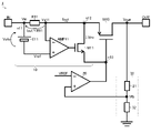
- FIG. 1 is a diagram showing a first comparative example of an overcurrent protection circuit.
- FIG. 2 is a diagram showing overcurrent protection characteristics of the first comparative example.
- FIG. 3 is a diagram showing a first embodiment of an overcurrent protection circuit.
- FIG. 4 is a diagram showing overcurrent protection characteristics of the first embodiment.
- FIG. 5 is a diagram showing a first modification of the first embodiment.
- FIG. 6 is a diagram showing a second modification of the first embodiment.
- FIG. 7 is a diagram showing a second embodiment of an overcurrent protection circuit.
- FIG. 8 is a diagram showing a second comparative example of the overcurrent protection circuit.
- FIG. 9 is a diagram showing overcurrent protection characteristics of the second comparative example.
- FIG. 10 is a diagram showing a third embodiment of an overcurrent protection circuit.
- FIG. 10 is a diagram showing a third embodiment of an overcurrent protection circuit.
- FIG. 11 is a diagram showing overcurrent protection characteristics of the third embodiment.
- FIG. 12 is a diagram showing a modification of the second embodiment.
- FIG. 13 is a diagram showing a fourth embodiment of an overcurrent protection circuit.
- FIG. 14 is a diagram showing a first application example of the semiconductor device.
- FIG. 15 is a diagram showing a second application example of the semiconductor device.
- the overcurrent protection circuit 10 of the first comparative example is a circuit block incorporated in the semiconductor device 1 together with the output transistor M10 (PMOSFET [P-channel type metal oxide semiconductor field effect transistor] in the example of this figure). It has an AMP11, a voltage source E11, an overcurrent protection transistor M11 (an NMOSFET [N-channel type MOSFET] in the example of this figure), and an overcurrent detection resistor R11.
- PMOSFET P-channel type metal oxide semiconductor field effect transistor
- the semiconductor device 1 incorporates a driver 20 and a feedback voltage generator 30, and operates as an LDO [low dropout] regulator.
- the driver 20 controls the driving of the output transistor M10 so as to generate a desired output voltage Vout from the input voltage Vin input to the input terminal IN and output it from the output terminal OUT.
- the driver 20 is configured so that the feedback voltage Vfb input to the non-inverting input terminal (+) and the reference voltage VREF input to the inverting input terminal (-) are imaginarily short-circuited. It is an operational amplifier that generates a gate signal for the output transistor M10.
- the feedback voltage generator 30 includes resistors 31 and 32 connected in series between the output terminal OUT and the ground terminal, and divides the output voltage Vout to generate the feedback voltage Vfb. Note that the output voltage Vout may be directly input to the driver 20 by omitting the feedback voltage generator 30 .
- the node n11 is connected to the input terminal IN.
- the negative terminal of the voltage source E11 is connected to the non-inverting input terminal (+) of the operational amplifier AMP11.
- the output terminal of the operational amplifier AMP11 is connected to the gate of the overcurrent protection transistor M11.
- the drain of the output transistor M10 is connected to the output terminal OUT.
- the operational amplifier AMP11 responds to the difference between the reference voltage Vref input from the negative terminal of the voltage source E11 to the non-inverting input terminal (+) and the detection voltage Vs11 input from the node n12 to the inverting input terminal (-). It controls the ON resistance (conductivity) of the overcurrent protection transistor M11.
- the gate control of the overcurrent protection transistor M11 is balanced in a state where the detection voltage Vs11 and the reference voltage Vref are imaginary shorted.
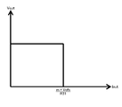
- FIG. 2 is a diagram showing overcurrent protection characteristics of the first comparative example.
- the horizontal axis indicates the output current Iout, and the vertical axis indicates the output voltage Vout.
- a so-called drooping output current limit is applied so that the output current Iout does not exceed a predetermined upper limit value ( ⁇ Vofs/R11). It is assumed that the drive current Idrv that flows during the overcurrent protection operation is so small that it can be ignored with respect to the output current Iout.
- overcurrent protection circuit 10 of the first comparative example it is possible to suppress an increase in the output current Iout due to an output abnormality or the like.
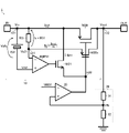
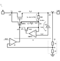
- FIG. 3 is a diagram showing a first embodiment of an overcurrent protection circuit.
- the overcurrent protection circuit 10 of the first embodiment is based on the first comparative example (FIG. 1) and further has a hysteresis setting resistor R12. Therefore, the same reference numerals as those in FIG. 1 are given to the components that have already been described to omit redundant description, and the characteristic portions of the first embodiment will be mainly described below.
- the output signal of the operational amplifier AMP11 rises from the low level according to the difference value between the two voltages.
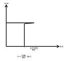
- FIG. 4 is a diagram showing overcurrent protection characteristics of the first embodiment. 2, the horizontal axis indicates the output current Iout, and the vertical axis indicates the output voltage Vout.
- the overcurrent protection circuit 10 of the first embodiment once the output current Iout reaches the overcurrent detection value ( ⁇ Vofs/R11), the output current Iout becomes lower than the overcurrent detection value.
- a so-called hysteresis-type output current limit is imposed so that a low predetermined upper limit value ( ⁇ (Vofs ⁇ Idrv ⁇ R12)/R11) is not exceeded.
- the overcurrent protection circuit 10 of the first embodiment it is possible to suppress an increase in the output current Iout due to an output abnormality or the like. ), the heat generation (power consumption) of the output transistor M10 can be suppressed.
- FIG. 5 is a diagram showing a first modification of the first embodiment.
- a P-channel overcurrent protection transistor M12 is used in place of the N-channel overcurrent protection transistor M11.
- an operational amplifier AMP12 whose input polarity is inverted may be used instead of the previously described operational amplifier AMP11.
- the source of the overcurrent protection transistor M12 and the non-inverting input terminal (+) of the operational amplifier AMP12 are both connected to the node n12 via the hysteresis setting resistor R12.
- the negative terminal of the voltage source E11 is connected to the inverting input terminal (-) of the operational amplifier AMP12.
- the output terminal of the operational amplifier AMP12 is connected to the gate of the overcurrent protection transistor M12. Both the gate of the output transistor M10 and the drain of the overcurrent protection transistor M12 are connected to the node n13.
- FIG. 6 is a diagram showing a second modification of the first embodiment.
- the output transistor M10, the overcurrent detection resistor R11, and the hysteresis setting resistor R12 may be externally attached to the semiconductor device 1, respectively.
- the semiconductor device 1 may be provided with external terminals T1 to T4 for externally connecting the output transistor M10, the overcurrent detection resistor R11, and the hysteresis setting resistor R12.
- the external terminal T1 is connected to the first end of the overcurrent detection resistor R11.
- the external terminal T2 is connected to the second terminal of the overcurrent detection resistor R11 and the source of the output transistor M10 via the hysteresis setting resistor R12.
- the external terminal T3 is connected to the gate of the output transistor M10.
- the external terminal T4 is connected to the drain of the output transistor M10.
- the external terminal T1 is connected to the positive terminal of the voltage source E11.
- the external terminal T2 is connected to the drain of the overcurrent protection transistor M11 and the inverting input terminal (-) of the operational amplifier AMP11.
- the external terminal T3 is connected to the source of the overcurrent protection transistor M11.
- the external terminal T4 is connected to the feedback voltage generator 30 . That is, the external terminals T1 to T3 should be provided corresponding to the nodes n11 to n13, respectively.
- the output transistor M10, the overcurrent detection resistor R11, and the hysteresis setting resistor R12 are all externally attached, but the output transistor M10 and the overcurrent detection resistor R11 may be individually externally attached. . If the hysteresis setting resistor R12 is externally attached, the overcurrent detection resistor R11 must also be externally attached.
- FIG. 7 is a diagram showing a second embodiment of an overcurrent protection circuit.
- the overcurrent protection circuit 10 of the second embodiment is a circuit block built into the semiconductor device 1 together with the output transistor M20 (NMOSFET in the example of this figure), and includes an operational amplifier AMP21, a voltage source E21, and an overcurrent protection transistor M21. (NMOSFET in the example of this figure), an overcurrent detection resistor R21, and a hysteresis setting resistor R22.
- the node n21 is connected to the output terminal OUT.
- the positive terminal of the voltage source E21 is connected to the inverting input terminal (-) of the operational amplifier AMP21.
- the output terminal of the operational amplifier AMP21 is connected to the gate of the overcurrent protection transistor M21.
- the drain of the output transistor M20 is connected to the input terminal IN.
- the operational amplifier AMP21 determines the on-resistance of the overcurrent protection transistor M21 ( conductivity).
- the output current Iout reaches the overcurrent detection value ( ⁇ Vofs/R21)
- the output current Iout reaches a predetermined upper limit value ( ⁇ Vofs/R21) lower than the overcurrent detection value.
- a so-called hysteresis type output current limit is applied so that (Vofs-Idrv ⁇ R22)/R21) is not exceeded.
- overcurrent protection circuit 10 of the second embodiment as in the first embodiment (FIG. 3), it is possible to suppress an increase in the output current Iout due to an output abnormality or the like. It is also possible to suppress heat generation (power consumption) of the output transistor M20 compared to the first comparative example (FIG. 2) having overcurrent protection characteristics.
- the output transistor M20, the overcurrent detection resistor R21, and the hysteresis setting resistor R22 may be externally attached to the semiconductor device 1 following FIG.
- the overcurrent protection circuit 10 of the second comparative example is a circuit block incorporated in the semiconductor device 1 together with the output transistor M30 (PMOSFET in this drawing), and includes a mirror transistor M30x (PMOSFET in this drawing), an operational amplifier AMP31, and a voltage It has a source E31, an overcurrent protection transistor M31 (NMOSFET in this figure), and an overcurrent detection resistor R31.
- the node n31 is connected to the input terminal IN.
- the drains of the output transistor M30 and the mirror transistor M30x are both connected to a node n32 (corresponding to a second node).
- the node n32 is connected to the output terminal OUT.
- the gates of the output transistor M30 and the mirror transistor M30x and the source of the overcurrent protection transistor M31 are both connected to a node n33 (corresponding to a third node).
- the source of the mirror transistor M30x, the second terminal of the overcurrent detection resistor R31, and the inverting input terminal (-) of the operational amplifier AMP31 are all connected to the node n34 (corresponding to the fourth node).
- the negative terminal of the voltage source E31 is connected to the non-inverting input terminal (+) of the operational amplifier AMP31.
- the output terminal of the operational amplifier AMP31 is connected to the gate of the overcurrent protection transistor M31.
- the operational amplifier AMP31 responds to the difference between the reference voltage Vref input from the negative terminal of the voltage source E31 to the non-inverting input terminal (+) and the detection voltage Vs31 input from the node n34 to the inverting input terminal (-). It controls the ON resistance (conductivity) of the overcurrent protection transistor M31.
- the output current Iout increases due to an output abnormality or the like
- the voltage across the overcurrent detection resistor R31 becomes higher than the offset voltage Vofs
- the detection voltage Vs31 becomes higher than the reference voltage Vref. becomes low
- the output signal of the operational amplifier AMP31 rises from the low level according to the difference value between the two voltages.
- the overcurrent protection transistor M31 is turned on, and the driving current Idrv flows between the gate and source of the output transistor M30, thereby lowering the voltage between the gate and source of the output transistor M30.
- the gate control of the overcurrent protection transistor M31 is balanced in a state where the detection voltage Vs31 and the reference voltage Vref are imaginary shorted.
- FIG. 9 is a diagram showing overcurrent protection characteristics of the second comparative example.
- the horizontal axis indicates the output current Iout, and the vertical axis indicates the output voltage Vout.
- a so-called drooping type output current limit is applied so that the output current Iout does not exceed a predetermined upper limit value ( ⁇ m ⁇ Vofs/R31). It hangs. It is assumed that the drive current Idrv that flows during the overcurrent protection operation is so small that it can be ignored with respect to the output current Iout.
- the overcurrent protection circuit 10 of the second comparative example it is possible to suppress an increase in the output current Iout due to an output abnormality or the like. Moreover, unlike the first comparative example (FIG. 1), the overcurrent detection resistor R31 is not inserted in the path through which the output current Iout flows, so it is possible to reduce power loss.
- FIG. 10 is a diagram showing a third embodiment of an overcurrent protection circuit.
- the overcurrent protection circuit 10 of the third embodiment is based on the above second comparative example (FIG. 8), but the connection destination of the drain of the overcurrent protection transistor M31 is changed from the node n31 to the node n34.
- the characteristic operation of the third embodiment associated with this change will be mainly described below.
- the overcurrent detection resistor R31 and the mirror transistor M30x are connected in series between the nodes n31 and n32. is being output.
- the operational amplifier AMP31 receives the reference voltage Vref input from the negative terminal of the voltage source E31 to the non-inverting input terminal (+) and the inverting input terminal (-) from the node n34.
- the ON resistance (conductivity) of the overcurrent protection transistor M31 is controlled according to the difference value from the detection voltage Vs31. This operation itself is the same as that of the second comparative example (FIG. 8).
- the overcurrent protection circuit 10 of the third embodiment when the overcurrent protection transistor M31 is in the ON state, the connection destination of the drain of the overcurrent protection transistor M31 is changed from the node n31 to the node n34.
- the overcurrent detection resistor R31 has both the functions of the overcurrent detection resistor R11 and the hysteresis setting resistor R12 of the first embodiment (FIG. 3). A specific description will be given below with reference to this drawing.
- FIG. 11 is a diagram showing overcurrent protection characteristics of the third embodiment. As in FIG. 9, the horizontal axis indicates the output current Iout, and the vertical axis indicates the output voltage Vout.
- the behavior until the output current Iout reaches a predetermined overcurrent detection value is No difference from Comparative Example 2 (FIG. 9).
- the behavior after the output current Iout reaches the overcurrent detection value is significantly different from that of the second comparative example (FIG. 9).
- the overcurrent protection circuit 10 of the third embodiment once the output current Iout reaches the overcurrent detection value ( ⁇ m ⁇ Vofs/R31), the output current Iout decreases to the overcurrent detection value A so-called hysteresis-type output current limit is applied so that a predetermined upper limit value ( ⁇ m ⁇ (Vofs/R31) ⁇ Idrv ⁇ ) lower than the current is not exceeded.
- FIG. 12 is a diagram showing a modification of the third embodiment.
- a P-channel overcurrent protection transistor M32 is used instead of the N-channel overcurrent protection transistor M31.
- an operational amplifier AMP32 whose input polarity is inverted may be used instead of the previously described operational amplifier AMP31.
- the source of the overcurrent protection transistor M32 and the non-inverting input terminal (+) of the operational amplifier AMP32 are both connected to the node n34.
- the negative terminal of the voltage source E31 is connected to the inverting input terminal (-) of the operational amplifier AMP32.
- the output terminal of the operational amplifier AMP32 is connected to the gate of the overcurrent protection transistor M32.
- the gates of the output transistor M30 and the mirror transistor M30x and the drain of the overcurrent protection transistor M32 are all connected to the node n33.
- FIG. 13 is a diagram showing a fourth embodiment of an overcurrent protection circuit.
- the overcurrent protection circuit 10 of the fourth embodiment is a circuit block incorporated in the semiconductor device 1 together with the output transistor M40 (NMOSFET in this figure), and includes a mirror transistor M40x (NMOSFET in this figure), an operational amplifier AMP41, and a voltage It has a source E41, an overcurrent protection transistor M41 (NMOSFET in this figure), and an overcurrent detection resistor R41.
- the node n41 is connected to the output terminal OUT.
- the node n42 is connected to the input terminal IN.
- the gates of the output transistor M40 and the mirror transistor M40x and the drain of the overcurrent protection transistor M41 are both connected to a node n43 (corresponding to a third node).
- the positive terminal of the voltage source E41 is connected to the inverting input terminal (-) of the operational amplifier AMP41.
- the output terminal of the operational amplifier AMP41 is connected to the gate of the overcurrent protection transistor M41.
- the operational amplifier AMP41 responds to the difference between the reference voltage Vref input from the positive terminal of the voltage source E41 to the inverting input terminal (-) and the detection voltage Vs41 input from the node n44 to the non-inverting input terminal (+). It controls the ON resistance (conductivity) of the overcurrent protection transistor M41.
- FIG. 14 is a diagram showing a first application example of the semiconductor device 1 (application example as an LDO [low drop out] regulator). As shown in the figure, the semiconductor device 1 of the first application example has the same configuration as that of the first embodiment (FIG. 3) described above. The drive control of the output transistor M10 is performed so as to generate the voltage Vout and supply it to the load 2 externally connected to the output terminal OUT.
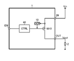
- FIG. 15 is a diagram showing a second application example (application example as a load switch) of the semiconductor device 1.
- FIG. As shown in the figure, the semiconductor device 1 of the second application example incorporates a controller 40 in place of the driver 20 while being based on the first embodiment (FIG. 3).
- the controller 40 performs on/off control of the output transistor M10 according to an enable signal externally input to the enable terminal EN.
- the semiconductor device 1 is used as a high-side switch. It is also possible to use the semiconductor device 1 as a low-side switch.
- the semiconductor device 1 of the second embodiment (FIG. 7), the third embodiment (FIG. 10), and the fourth embodiment (FIG. 13) also has an LDO regulator or a high-side switch (or a low-side switch). switch).
- FIGS. 14 and 15 only the output transistor M10 is illustrated as an object to be driven by the driver 20 and the controller 40, but the semiconductor device 1 of the third embodiment (FIG. 10) is used instead of the first embodiment (FIG. 3). is used, that is, when the overcurrent protection circuit 10 includes the mirror transistor M30x, both the output transistor M30 and the mirror transistor M30x are driven by the driver 20 and the controller 40, and synchronous drive control by the driver 20 and the controller 40 is performed. will take place.
- the overcurrent protection circuit disclosed herein includes a first node configured to connect a first end of an overcurrent sense resistor, a second end of the overcurrent sense resistor and an output. a second node to which the main electrodes of the transistors are commonly connected; a third node to which the control electrodes of the output transistors are connected; and an offset voltage at the terminal voltage of the first node. and a voltage source connected in series between the second node and the third node to output a detected voltage from a fourth node therebetween.
- a configuration (first configuration ).
- the operational amplifier fully turns off the overcurrent protection transistor until the voltage across the overcurrent detection resistor exceeds the offset voltage. Once the voltage exceeds the offset voltage, the overcurrent protection transistor is turned on so that the sum of the voltage across the overcurrent detection resistor and the voltage across the hysteresis setting resistor matches the offset voltage.
- a configuration (second configuration) that controls the resistance may be employed.
- the offset voltage is set such that the voltage across the hysteresis setting resistor during overcurrent protection operation is lower than the on-threshold voltage of the output transistor.
- a configuration (third configuration) may be used.
- the semiconductor device disclosed in this specification has a configuration (fourth configuration) having an overcurrent protection circuit according to any one of the first to third configurations.
- the semiconductor device according to the fourth configuration may have a configuration (fifth configuration) in which both the output transistor and the overcurrent detection resistor are incorporated.
- the semiconductor device according to the fourth configuration may be configured to have a plurality of external terminals configured to externally attach the output transistor and the overcurrent detection resistor (sixth configuration).
- the semiconductor device further includes a driver for controlling the driving of the output transistor so as to generate a desired output voltage from the input voltage (seventh configuration). good too.
- the semiconductor device may further include a controller for controlling on/off of the output transistor according to an enable signal (eighth configuration).
- a first node configured to connect a first main electrode of an output transistor and a second main electrode of the output transistor are connected.
- a second node configured to be connected to the control electrode of the output transistor;
- a third node configured to be connected to the control electrode of the output transistor; and
- an overcurrent detection resistor and mirror connected in series between the first node and the second node and configured to output a detection voltage from a fourth node therebetween.
- a transistor, an overcurrent protection transistor configured to be connected between the fourth node and the third node, and operating the overcurrent protection transistor according to a difference value between the reference voltage and the detection voltage. and an operational amplifier configured to control (ninth configuration).
- the operational amplifier fully turns off the overcurrent protection transistor until the voltage across the overcurrent detection resistor exceeds the offset voltage. Once the voltage exceeds the offset voltage, the on-resistance of the overcurrent protection transistor may be controlled so that the voltage across the overcurrent detection resistor matches the offset voltage (a tenth configuration). .
- the offset voltage is set such that the voltage across the overcurrent detection resistor during overcurrent protection operation is lower than the ON threshold voltage of the output transistor.
- a configuration (eleventh configuration) may be used.
- the semiconductor device disclosed in this specification has a configuration (a twelfth configuration) including the output transistor and an overcurrent protection circuit according to any one of the ninth to eleventh configurations.
- the semiconductor device may further include a driver for driving and controlling the output transistor and the mirror transistor so as to generate a desired output voltage from the input voltage (the thirteenth configuration). good.
- the semiconductor device according to the twelfth configuration may further include a controller that performs on/off control of the output transistor and the mirror transistor according to an enable signal (fourteenth configuration).
Landscapes
- Engineering & Computer Science (AREA)
- Physics & Mathematics (AREA)
- Electromagnetism (AREA)
- General Physics & Mathematics (AREA)
- Radar, Positioning & Navigation (AREA)
- Automation & Control Theory (AREA)
- Microelectronics & Electronic Packaging (AREA)
- Nonlinear Science (AREA)
- Continuous-Control Power Sources That Use Transistors (AREA)
Priority Applications (4)
| Application Number | Priority Date | Filing Date | Title |
|---|---|---|---|
| CN202280044170.2A CN117561486A (zh) | 2021-06-29 | 2022-05-23 | 过电流保护电路和半导体装置 |
| DE112022002489.5T DE112022002489T5 (de) | 2021-06-29 | 2022-05-23 | Überstromschutzschaltung und halbleitervorrichtung |
| JP2023531710A JPWO2023276491A1 (https=) | 2021-06-29 | 2022-05-23 | |
| US18/544,977 US20240160237A1 (en) | 2021-06-29 | 2023-12-19 | Overcurrent protection circuit and semiconductor device |
Applications Claiming Priority (4)
| Application Number | Priority Date | Filing Date | Title |
|---|---|---|---|
| JP2021107634 | 2021-06-29 | ||
| JP2021107635 | 2021-06-29 | ||
| JP2021-107635 | 2021-06-29 | ||
| JP2021-107634 | 2021-06-29 |
Related Child Applications (1)
| Application Number | Title | Priority Date | Filing Date |
|---|---|---|---|
| US18/544,977 Continuation US20240160237A1 (en) | 2021-06-29 | 2023-12-19 | Overcurrent protection circuit and semiconductor device |
Publications (1)
| Publication Number | Publication Date |
|---|---|
| WO2023276491A1 true WO2023276491A1 (ja) | 2023-01-05 |
Family
ID=84691256
Family Applications (1)
| Application Number | Title | Priority Date | Filing Date |
|---|---|---|---|
| PCT/JP2022/021091 Ceased WO2023276491A1 (ja) | 2021-06-29 | 2022-05-23 | 過電流保護回路、半導体装置 |
Country Status (4)
| Country | Link |
|---|---|
| US (1) | US20240160237A1 (https=) |
| JP (1) | JPWO2023276491A1 (https=) |
| DE (1) | DE112022002489T5 (https=) |
| WO (1) | WO2023276491A1 (https=) |
Citations (4)
| Publication number | Priority date | Publication date | Assignee | Title |
|---|---|---|---|---|
| JPH05315852A (ja) * | 1992-05-12 | 1993-11-26 | Fuji Electric Co Ltd | 電流制限回路および電流制限回路用定電圧源 |
| JP2003216252A (ja) * | 2001-11-15 | 2003-07-31 | Seiko Instruments Inc | ボルテージレギュレータ |
| JP2005157743A (ja) * | 2003-11-26 | 2005-06-16 | Fujitsu Ten Ltd | 負荷駆動装置及び負荷駆動システム |
| JP2012159870A (ja) * | 2011-01-28 | 2012-08-23 | Seiko Instruments Inc | ボルテージレギュレータ |
Family Cites Families (1)
| Publication number | Priority date | Publication date | Assignee | Title |
|---|---|---|---|---|
| JP4286763B2 (ja) | 2004-10-15 | 2009-07-01 | ローム株式会社 | 過電流保護回路および電圧生成回路 |
-
2022
- 2022-05-23 WO PCT/JP2022/021091 patent/WO2023276491A1/ja not_active Ceased
- 2022-05-23 DE DE112022002489.5T patent/DE112022002489T5/de not_active Withdrawn
- 2022-05-23 JP JP2023531710A patent/JPWO2023276491A1/ja active Pending
-
2023
- 2023-12-19 US US18/544,977 patent/US20240160237A1/en active Pending
Patent Citations (4)
| Publication number | Priority date | Publication date | Assignee | Title |
|---|---|---|---|---|
| JPH05315852A (ja) * | 1992-05-12 | 1993-11-26 | Fuji Electric Co Ltd | 電流制限回路および電流制限回路用定電圧源 |
| JP2003216252A (ja) * | 2001-11-15 | 2003-07-31 | Seiko Instruments Inc | ボルテージレギュレータ |
| JP2005157743A (ja) * | 2003-11-26 | 2005-06-16 | Fujitsu Ten Ltd | 負荷駆動装置及び負荷駆動システム |
| JP2012159870A (ja) * | 2011-01-28 | 2012-08-23 | Seiko Instruments Inc | ボルテージレギュレータ |
Also Published As
| Publication number | Publication date |
|---|---|
| DE112022002489T5 (de) | 2024-03-07 |
| JPWO2023276491A1 (https=) | 2023-01-05 |
| US20240160237A1 (en) | 2024-05-16 |
Similar Documents
| Publication | Publication Date | Title |
|---|---|---|
| CN113110694B (zh) | 一种具有电流浪涌抑制的低压差线性稳压器电路 | |
| US7602162B2 (en) | Voltage regulator with over-current protection | |
| US7385378B2 (en) | Constant-voltage circuit, semiconductor device using the same, and constant-voltage outputting method providing a predetermined output voltage | |
| CN102455728B (zh) | 电流控制电路 | |
| US7893672B2 (en) | Technique to improve dropout in low-dropout regulators by drive adjustment | |
| JP3394509B2 (ja) | 定電圧電源 | |
| TWI476558B (zh) | 電壓調節器 | |
| JP5008472B2 (ja) | ボルテージレギュレータ | |
| JP4443301B2 (ja) | ボルテージ・レギュレータ | |
| US8665020B2 (en) | Differential amplifier circuit that can change current flowing through a constant-current source according to load variation, and series regulator including the same | |
| JP5279544B2 (ja) | ボルテージレギュレータ | |
| JP5631918B2 (ja) | 過電流保護回路、および、電力供給装置 | |
| JP6180815B2 (ja) | ボルテージレギュレータ | |
| JP5444869B2 (ja) | 出力装置 | |
| JP2017126259A (ja) | 電源装置 | |
| JP2008276566A (ja) | 定電圧電源回路 | |
| KR20150123712A (ko) | 과전류 보호 회로, 반도체 장치 및 볼티지 레귤레이터 | |
| WO2021049135A1 (ja) | 過電流保護回路 | |
| JP2013058093A (ja) | 定電圧電源回路 | |
| JP7173915B2 (ja) | 電源回路 | |
| US20050151522A1 (en) | Constant-voltage power supply circuit | |
| US10551860B2 (en) | Regulator for reducing power consumption | |
| WO2023276491A1 (ja) | 過電流保護回路、半導体装置 | |
| JP2010217965A (ja) | 定電圧回路 | |
| JP2011118865A (ja) | 過電流保護回路及び定電圧電源回路 |
Legal Events
| Date | Code | Title | Description |
|---|---|---|---|
| 121 | Ep: the epo has been informed by wipo that ep was designated in this application |
Ref document number: 22832649 Country of ref document: EP Kind code of ref document: A1 |
|
| WWE | Wipo information: entry into national phase |
Ref document number: 2023531710 Country of ref document: JP |
|
| WWE | Wipo information: entry into national phase |
Ref document number: 202280044170.2 Country of ref document: CN |
|
| WWE | Wipo information: entry into national phase |
Ref document number: 112022002489 Country of ref document: DE |
|
| 122 | Ep: pct application non-entry in european phase |
Ref document number: 22832649 Country of ref document: EP Kind code of ref document: A1 |