WO2023276106A1 - 半導体光デバイス - Google Patents
半導体光デバイス Download PDFInfo
- Publication number
- WO2023276106A1 WO2023276106A1 PCT/JP2021/024936 JP2021024936W WO2023276106A1 WO 2023276106 A1 WO2023276106 A1 WO 2023276106A1 JP 2021024936 W JP2021024936 W JP 2021024936W WO 2023276106 A1 WO2023276106 A1 WO 2023276106A1
- Authority
- WO
- WIPO (PCT)
- Prior art keywords
- core
- optical
- substrate
- clad layer
- semiconductor
- Prior art date
- Legal status (The legal status is an assumption and is not a legal conclusion. Google has not performed a legal analysis and makes no representation as to the accuracy of the status listed.)
- Ceased
Links
Images





Classifications
-
- H—ELECTRICITY
- H01—ELECTRIC ELEMENTS
- H01S—DEVICES USING THE PROCESS OF LIGHT AMPLIFICATION BY STIMULATED EMISSION OF RADIATION [LASER] TO AMPLIFY OR GENERATE LIGHT; DEVICES USING STIMULATED EMISSION OF ELECTROMAGNETIC RADIATION IN WAVE RANGES OTHER THAN OPTICAL
- H01S5/00—Semiconductor lasers
- H01S5/02—Structural details or components not essential to laser action
- H01S5/026—Monolithically integrated components, e.g. waveguides, monitoring photo-detectors, drivers
-
- G—PHYSICS
- G02—OPTICS
- G02B—OPTICAL ELEMENTS, SYSTEMS OR APPARATUS
- G02B6/00—Light guides; Structural details of arrangements comprising light guides and other optical elements, e.g. couplings
- G02B6/10—Light guides; Structural details of arrangements comprising light guides and other optical elements, e.g. couplings of the optical waveguide type
- G02B6/12—Light guides; Structural details of arrangements comprising light guides and other optical elements, e.g. couplings of the optical waveguide type of the integrated circuit kind
- G02B6/122—Basic optical elements, e.g. light-guiding paths
- G02B6/125—Bends, branchings or intersections
-
- H—ELECTRICITY
- H01—ELECTRIC ELEMENTS
- H01S—DEVICES USING THE PROCESS OF LIGHT AMPLIFICATION BY STIMULATED EMISSION OF RADIATION [LASER] TO AMPLIFY OR GENERATE LIGHT; DEVICES USING STIMULATED EMISSION OF ELECTROMAGNETIC RADIATION IN WAVE RANGES OTHER THAN OPTICAL
- H01S5/00—Semiconductor lasers
- H01S5/02—Structural details or components not essential to laser action
- H01S5/0206—Substrates, e.g. growth, shape, material, removal or bonding
- H01S5/021—Silicon based substrates
-
- H—ELECTRICITY
- H01—ELECTRIC ELEMENTS
- H01S—DEVICES USING THE PROCESS OF LIGHT AMPLIFICATION BY STIMULATED EMISSION OF RADIATION [LASER] TO AMPLIFY OR GENERATE LIGHT; DEVICES USING STIMULATED EMISSION OF ELECTROMAGNETIC RADIATION IN WAVE RANGES OTHER THAN OPTICAL
- H01S5/00—Semiconductor lasers
- H01S5/10—Construction or shape of the optical resonator, e.g. extended or external cavity, coupled cavities, bent-guide, varying width, thickness or composition of the active region
- H01S5/1028—Coupling to elements in the cavity, e.g. coupling to waveguides adjacent the active region, e.g. forward coupled [DFC] structures
- H01S5/1032—Coupling to elements comprising an optical axis that is not aligned with the optical axis of the active region
-
- H—ELECTRICITY
- H01—ELECTRIC ELEMENTS
- H01S—DEVICES USING THE PROCESS OF LIGHT AMPLIFICATION BY STIMULATED EMISSION OF RADIATION [LASER] TO AMPLIFY OR GENERATE LIGHT; DEVICES USING STIMULATED EMISSION OF ELECTROMAGNETIC RADIATION IN WAVE RANGES OTHER THAN OPTICAL
- H01S5/00—Semiconductor lasers
- H01S5/20—Structure or shape of the semiconductor body to guide the optical wave ; Confining structures perpendicular to the optical axis, e.g. index or gain guiding, stripe geometry, broad area lasers, gain tailoring, transverse or lateral reflectors, special cladding structures, MQW barrier reflection layers
- H01S5/22—Structure or shape of the semiconductor body to guide the optical wave ; Confining structures perpendicular to the optical axis, e.g. index or gain guiding, stripe geometry, broad area lasers, gain tailoring, transverse or lateral reflectors, special cladding structures, MQW barrier reflection layers having a ridge or stripe structure
- H01S5/223—Buried stripe structure
Definitions
- the present invention relates to semiconductor optical devices.
- Si photonics is a technology that integrates electronic devices and optical devices on a large-diameter Si substrate using CMOS technology. Since Si is an indirect transition semiconductor, its luminous efficiency is extremely low, making it difficult to use Si as a light emitting device. For this reason, III-V group compound semiconductors such as GaAs and InP, which are direct transition type semiconductors and have high luminous efficiency, are used as optical devices.
- Non-Patent Document 1 as an optical device of Si photonics, it is possible to fabricate a laser structure on an SiO 2 /Si substrate by bonding an InP substrate and an SiO 2 /Si substrate. Hydrophilic bonding and surface activation bonding are available as substrate bonding techniques. A layer made of an insulating material such as SiO 2 is used at the joint interface in these joints.
- the refractive index of the Si substrate is higher than the refractive index of the upper cladding medium and comparable to the refractive index of the active layer medium. Therefore, in order to obtain high optical confinement in the active layer, the thickness of SiO 2 should be on the order of several ⁇ m, and the design should be such that the waveguide mode is not distributed in the Si substrate. For example, in a membrane laser structure on a SiO 2 /Si substrate, since the active layer is sandwiched between layers of low refractive index media, a high optical confinement factor can be obtained. Therefore, a direct modulation laser with high efficiency and low power consumption has been realized (Non-Patent Document 1).
- the thermal conductivity of SiO 2 is small, so the heat dissipation effect in the active layer is small. Therefore, there is a problem that the temperature rise due to current injection is large, and the light output and the modulation speed are saturated with a relatively small bias current.
- Non-Patent Document 3 a direct modulation laser with a bandwidth of 60 GHz has been realized because more current can be injected than in the conventional structure.
- a laser formed on a heat - dissipating substrate can be expected to have excellent operating characteristics as a single optical element. It is difficult to optically couple to the Si optical waveguide embedded in 2 , and application to Si photonics is a problem.
- the amount of current that can be injected into the semiconductor laser section increases due to the high heat dissipation in the active layer, so high optical output, high-speed modulation, and high-temperature operation are possible. can be expected.
- Si photonics simply by arranging a laser on a heat-dissipating layer.
- there is a problem that such optical coupling is not easy.
- the present invention has been made to solve the above-described problems, and facilitates optical coupling between an optical element and a Si optical waveguide, which are arranged with a layer having a high heat dissipation property in between.
- the purpose is to obtain
- a semiconductor optical device comprises: a first clad layer formed on a Si substrate and made of a material having higher thermal conductivity than a direct transition semiconductor; A core made of a transition type semiconductor, and a second clad layer covering the core and formed on the first clad layer, wherein the refractive index of the first clad layer is higher than that of the second clad layer, and the core In the optical coupling region of the optical waveguide by the core, the cross-sectional shape of the core is in a state in which the substrate radiation mode is expressed.
- the optical coupling between the optical element and the Si optical waveguide, which are arranged with a layer having high heat dissipation, can be obtained more easily.
- FIG. 1 is a cross-sectional view showing the configuration of a semiconductor optical device according to an embodiment of the present invention.
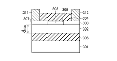
- FIG. 2A is a cross-sectional view showing the configuration of a semiconductor laser used for studying the heat dissipation characteristics of the semiconductor optical device according to the embodiment.
- FIG. 2B is a characteristic diagram showing the results of examination of the heat dissipation characteristics of the semiconductor optical device according to the embodiment.
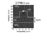
- FIG. 4A is a distribution diagram showing the calculation result of the substrate radiation mode profile in the optical waveguide by the core 103 with a core width of 0.5 ⁇ m.
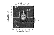
- FIG. 4B is a distribution diagram showing the calculation result of the substrate radiation mode profile in the optical waveguide by the core 103 with a core width of 0.4 ⁇ m.
- FIG. 4C is a distribution diagram showing the calculation result of the substrate radiation mode profile in the optical waveguide by the core 103 with a core width of 0.3 ⁇ m.
- FIG. 5A is a distribution diagram showing the calculation result of the substrate radiation mode profile in the optical waveguide by the core 103 with a core width of 0.5 ⁇ m.
- FIG. 5B is a distribution diagram showing the calculation results of the profile of the substrate radiation mode in the optical waveguide by the core 103 with a core width of 0.4 ⁇ m.
- FIG. 5C is a distribution diagram showing the calculation result of the substrate radiation mode profile in the optical waveguide by the core 103 with a core width of 0.3 ⁇ m.
- FIG. 5A is a distribution diagram showing the calculation result of the substrate radiation mode profile in the optical waveguide by the core 103 with a core width of 0.5 ⁇ m.
- FIG. 5B is a distribution diagram showing the calculation results of the profile of the substrate radiation mode in the optical waveguide by the core 103 with a core width of
- FIG. 6 is a cross-sectional view showing the configuration of another semiconductor optical device according to the embodiment of the invention.
- FIG. 7A is a distribution diagram showing calculation results of the mode profile when the core width of the core 103 is 0.7 ⁇ m and the core width of the lower core 107 is 0.3 ⁇ m.
- FIG. 7B is a distribution diagram showing calculation results of the mode profile when the core width of the core 103 is 0.5 ⁇ m and the core width of the lower core 107 is 0.3 ⁇ m.
- FIG. 7C is a distribution diagram showing calculation results of the mode profile when the core width of the core 103 is 0.3 ⁇ m and the core width of the lower core 107 is 0.3 ⁇ m.
- FIG. 7A is a distribution diagram showing calculation results of the mode profile when the core width of the core 103 is 0.7 ⁇ m and the core width of the lower core 107 is 0.3 ⁇ m.
- FIG. 7B is a distribution diagram showing calculation results of the mode profile when the core width of the core 103
- FIG. 7D is a distribution diagram showing calculation results of the mode profile when the core width of the core 103 is 0.3 ⁇ m and the core width of the lower core 107 is 0.35 ⁇ m.
- FIG. 7E is a distribution diagram showing calculation results of the mode profile when the core width of the core 103 is 0.3 ⁇ m and the core width of the lower core 107 is 0.4 ⁇ m.
- FIG. 8 is a distribution diagram showing calculation of mode transition from the optical waveguide by the core 103 to the optical waveguide by the lower core 107 when the rib structure is not provided.
- FIG. 9 is a cross-sectional view showing the configuration of another semiconductor optical device according to the embodiment of the invention.
- FIG. 10 is a cross-sectional view showing the configuration of another semiconductor optical device according to the embodiment of the invention.
- This semiconductor optical device comprises a first cladding layer 102 formed on a Si substrate 101, a core 103 formed on the first cladding layer 102, and a core 103 covering the first cladding layer 102. and a formed second cladding layer 104 .
- a lower clad layer 106 made of SiO 2 or the like is formed on the Si substrate 101 (surface), and a first clad layer 102 is formed on the lower clad layer 106 .
- the first cladding layer 102 is composed of a material with higher thermal conductivity than a direct transition semiconductor.
- the core 103 is composed of a direct transition semiconductor.
- the core 103 can be composed of, for example, III-V group compound semiconductors such as InP and InGaAsP.
- the core 103 is formed in contact with the active layer of the semiconductor laser not shown in FIG. A laser beam oscillated from a semiconductor laser is guided through the optical waveguide formed by the core 103 .
- the refractive index of the first clad layer 102 is higher than that of the second clad layer 104 and lower than that of the core 103 .
- the first clad layer 102 can be made of, for example, SiC, AlN, GaN, diamond, or the like.
- the second cladding layer 104 can be made of SiO2 , SiOx , or the like.
- FIG. 1 shows a cross section of the optical coupling region of this semiconductor optical device.
- the width of the core 103 in the planar direction of the Si substrate 101 is made smaller as it approaches the optical coupling region.
- a substrate radiation mode can be developed by reducing the width of the core 103 (core width).
- the core width of the core 103 in the optical coupling region can be 0.3 ⁇ m and the thickness can be 0.32 ⁇ m.
- the thickness of the core 103 of 0.32 ⁇ m is approximately the upper limit value at which light with a wavelength of 1.31 ⁇ m propagating in the active layer becomes single mode in the thickness direction of the active layer.
- the laser light guided through the optical waveguide by the core 103 is coupled to the optical waveguide by the lower core formed under the first clad layer 102 (not shown in FIG. 1). be able to.
- the optical waveguide by the lower core arranged under the first clad layer 102 is arranged so as to overlap the core 103 in the optical coupling region.
- the lower core may be made of Si and embedded in the lower clad layer 106 .
- the optical waveguide formed by the lower core is arranged in the optical coupling region within a range where it can be optically coupled with the optical waveguide formed by the core 103 .
- the first cladding layer 102 in the optical coupling region has a convexly thickened rib structure 105 on the surface, and the core 103 is formed on the rib structure 105 .
- the rib structure 105 can be formed by etching the first clad layer 102 using a resist pattern formed by a known lithography technique as a mask. The etching depth d etch in this etching process becomes the thickness of the rib structure 105 .
- the optical confinement in the lateral direction of the substrate radiation mode is improved, and the coupling of light by the substrate radiation mode described above can be implemented more efficiently.
- the above-described Optical coupling can be realized.
- the first grating coupler formed in the core 103 allows the laser light guided through the optical waveguide by the core 103 to be emitted to the Si substrate 101 side. Light thus emitted couples into a second grating coupler formed in the lower core.
- a core 103 and a semiconductor laser connected to the core 103 are fabricated on a substrate to be the first cladding layer 102, and a rib structure 105 is formed. 2 cladding layer 104 is formed.
- the first clad layer 102 is bonded to the Si substrate 101 on which the lower clad layer 106 is formed.
- the semiconductor optical device according to the embodiment can be produced.
- an optical waveguide can be formed by a lower core or the like before bonding.
- a so-called membrane laser structure consisting of an active layer 303 and a p-InP layer 307 and an n-InP layer 308 arranged with the active layer 303 interposed therebetween.
- the active layer 303 has, for example, a multiple quantum well structure of InGaAlAs or InGaAsP.
- the upper surface of the active layer 303 is covered with a semiconductor layer 309 made of non-doped InP.
- a second clad layer 304 made of SiO 2 is formed on the active layer 303 , p-InP layer 307 and n-InP layer 308 .
- a p-electrode 311 is ohmically connected to the p-InP layer 307
- an n-electrode 312 is ohmically connected to the n-InP layer 308 .
- the active layer 303 has a core shape with a core width of 0.7 ⁇ m and a thickness of 0.33 ⁇ m.
- FIG. 2B shows the d SiC dependence of the thermal resistance of a semiconductor laser with an active layer length of 50 ⁇ m in the waveguide direction. A heat source was placed only on the p-InP layer 307 and had a power of 100 mW. As shown in FIG. 2B, it is clear that the larger d SiC is, the smaller the thermal resistance value is. This indicates that the greater the thickness of the first cladding layer made of SiC, the greater the amount of current injected into the semiconductor laser, and the greater the relaxation oscillation frequency, thereby increasing the modulation band.
- the lower clad layer 106 was made of SiO2
- the first clad layer 102 was made of SiC
- the core 103 was made of InP
- the second clad layer 104 was made of SiOx .
- the core 103 has a core width of 0.3 ⁇ m and a thickness of 0.25 ⁇ m.
- the thickness of the first clad layer 102 was 2 ⁇ m
- the thickness of the lower clad layer 106 was 1 ⁇ m.
- a rib structure 105 was formed by etching a portion 2 ⁇ m away from the formation position of the core 103 in the planar direction.
- the waveguide mode is the substrate radiation mode. Further, when the rib structure 105 is formed, the lateral optical confinement of the first cladding layer 102 by SiC is enhanced. Therefore, the use of the rib structure 105 can effectively couple light through the optical waveguide of the lower core.
- FIG. 4A shows the calculation results of the profile of the substrate radiation mode in the optical waveguide with the core 103 having a core width of 0.5 ⁇ m.
- FIG. 4B shows the calculation result of the substrate radiation mode profile in the optical waveguide with the core 103 having a core width of 0.4 ⁇ m.
- FIG. 4c shows the calculated profile of the substrate radiation mode in the optical waveguide with the core 103 having a core width of 0.3 ⁇ m.
- the lower clad layer 106 was made of SiO2
- the first clad layer 102 was made of SiC
- the core 103 was made of InP
- the second clad layer 104 was made of SiOx .
- the core 103 has a thickness of 0.25 ⁇ m.
- the thickness of the first clad layer 102 was 2 ⁇ m
- the thickness of the lower clad layer 106 was 1 ⁇ m.
- a rib structure 105 was formed by etching a portion 2 ⁇ m away from the formation position of the core 103 in the plane direction, and the thickness of the rib structure 105 was set to 2 ⁇ m.
- modes are distributed in the optical waveguide by the core 103 when the core width is 0.5 ⁇ m.
- the substrate radiation mode occurs at core widths of 0.4 ⁇ m and 0.3 ⁇ m. Therefore, by setting the core width to about 0.5 ⁇ m in the region that is not the optical coupling region and gradually decreasing the width toward the optical coupling region, it is possible to gradually cause substrate radiation during mode propagation of the optical waveguide by the core 103 . is.
- the thickness of the first clad layer 102 made of SiC was set to 5 ⁇ m.
- FIG. 5A shows the calculation result of the profile of the substrate radiation mode in the optical waveguide by the core 103 with a core width of 0.5 ⁇ m.
- FIG. 5B shows the calculation result of the substrate radiation mode profile in the optical waveguide with the core 103 having a core width of 0.4 ⁇ m.
- FIG. 5c shows the calculated profile of the substrate radiation mode in the optical waveguide with the core 103 having a core width of 0.3 ⁇ m.
- the thickness of the first clad layer 102 is increased, substrate radiation occurs as the core width of the core 103 becomes narrower, similar to the results shown in FIGS. 4A, 4B, and 4C. Also, in this calculation result, it can be seen that the mode is confined in the lateral direction in the first clad layer 102 by using the rib structure 105 . By reducing the thickness of the core 103 in addition to its width, the substrate radiation mode is more efficiently generated.
- This semiconductor optical device comprises a lower clad layer 106 formed on a Si substrate 101, a first clad layer 102 formed on the lower clad layer 106, and a core 103 formed on the first clad layer 102. and a second clad layer 104 covering the core 103 and formed on the first clad layer 102 .
- a rib structure 105 is formed in the first clad layer 102 .
- a lower core 107 embedded in the lower clad layer 106 is provided on the Si substrate 101 under the first clad layer 102 .
- the lower core 107 is made of Si, for example.
- FIG. 6 shows a cross section of the optical coupling region of the semiconductor optical device.
- the core 103 is made of InP
- the lower core 107 is made of Si
- the first clad layer 102 is made of SiC
- the second clad layer 104 is made of SiOx
- the lower clad layer 106 is made of , SiO 2 .
- FIG. 7A shows the calculation result of the mode profile when the core width of the core 103 is 0.7 ⁇ m and the core width of the lower core 107 is 0.3 ⁇ m.
- FIG. 7B shows the calculation result of the mode profile when the core width of the core 103 is 0.5 ⁇ m and the core width of the lower core 107 is 0.3 ⁇ m.
- FIG. 7C shows the calculation result of the mode profile when the core width of the core 103 is 0.3 ⁇ m and the core width of the lower core 107 is 0.3 ⁇ m.
- FIG. 7D shows the calculation result of the mode profile when the core width of the core 103 is 0.3 ⁇ m and the core width of the lower core 107 is 0.35 ⁇ m.
- FIG. 7E shows the calculation result of the mode profile when the core width of the core 103 is 0.3 ⁇ m and the core width of the lower core 107 is 0.4 ⁇ m.
- the optical waveguide of the core 103 is reduced to the optical waveguide of the lower core 107. , it can be seen that the mode transitions efficiently.
- FIG. 8 shows mode transition from the optical waveguide by the core 103 to the optical waveguide by the lower core 107 when the rib structure is not provided.
- the core width of the core 103 is assumed to be 0.5 ⁇ m
- the core width of the lower core 107 is assumed to be 0.3 ⁇ m.
- the mode in the first cladding layer 102 spreads in the lateral direction compared to the case of using the rib structure. Therefore, the efficiency of mode transition from the optical waveguide by the core 103 to the optical waveguide by the lower core 107 is lowered.
- FIG. 9 schematically shows a cross section parallel to the waveguide.
- a semiconductor laser 112 having an active layer 111 having a multiple quantum well structure is formed on the first clad layer 102 , and a core 103 is formed optically connected to the semiconductor laser 112 .
- the semiconductor laser 112 is, for example, a distributed feedback (DFB) laser.
- the semiconductor laser 112 is covered with the second clad layer 104 together with the core 103 .
- the core width of the core 103 gradually decreases from the coupling point with the semiconductor laser 112 to the optical coupling region 121 .
- a lower core 107 is formed so as to overlap the core 103 vertically in the optical coupling region 121 .
- Lower core 107 extends from optical coupling region 121 in a direction away from semiconductor laser 112 .
- the first clad layer 102 and the second clad layer 104 are not formed.
- the waveguide mode becomes the substrate radiation mode, and can be coupled to the optical waveguide formed by the lower core 107 .
- the core width of the lower core 107 is, for example, 0.3 ⁇ m, which is smaller than that in other regions. Therefore, the waveguide mode transitions from the optical waveguide by the core 103 to the optical waveguide by the lower core 107 .
- an optical feedback section 113 is formed at a predetermined location in the extending region apart from the optical coupling region 121 in the waveguide direction of the lower core 107 .
- the optical feedback section 113 can be, for example, a DBR with a diffraction grating or a gap. Further, the optical feedback part 113 can be based on Fresnel reflection in the optical waveguide by the lower core 107 .
- the semiconductor laser 112 interacts with the Fabry-Perot resonance mode formed in the optical feedback section 113, and under the condition that the phase matching condition is satisfied, a photon-photon resonance phenomenon (photon-photon resonance; PPR) occurs.
- PPR photon-photon resonance
- the lower clad layer 106 where the optical feedback section 113 is formed by providing a heater 114 on the lower clad layer 106 where the optical feedback section 113 is formed and adjusting the temperature in the optical feedback section 113, it is possible to control the phase.
- the lower clad layer 106 made of SiO 2 has low thermal conductivity, it is possible to efficiently control the temperature of the optical feedback section 113 .
- the optical coupling described above can be made more efficient.
- the first grating coupler 115 formed in the core 103 can radiate the laser light guided through the optical waveguide by the core 103 to the Si substrate 101 side. This emitted light couples into a second grating coupler 116 formed in the lower core 107 .
- the coupled laser light is guided in the extending direction of the lower core 107 .
- the semiconductor optical device As described above, according to the semiconductor optical device according to the embodiment, from the semiconductor laser 112 formed on the first cladding layer 102 with high heat dissipation, through the optical waveguide of the core 103 , Si of the lower core 107 . It becomes possible to couple light to a laser with an optical waveguide, and a laser that operates in a wide band and at a high temperature can be applied to Si photonics.
- a first cladding layer made of a material having a higher thermal conductivity than a direct transition semiconductor is formed on a Si substrate, and a direct transition semiconductor is formed thereon.
- a core was formed, the refractive index of the first clad layer was made lower than that of the core, and the cross-sectional shape of the core was such that the substrate radiation mode was expressed in the optical coupling region of the optical waveguide by the core.
Landscapes
- Physics & Mathematics (AREA)
- General Physics & Mathematics (AREA)
- Optics & Photonics (AREA)
- Condensed Matter Physics & Semiconductors (AREA)
- Electromagnetism (AREA)
- Geometry (AREA)
- Engineering & Computer Science (AREA)
- Microelectronics & Electronic Packaging (AREA)
- Optical Integrated Circuits (AREA)
Priority Applications (3)
| Application Number | Priority Date | Filing Date | Title |
|---|---|---|---|
| JP2023531289A JP7647887B2 (ja) | 2021-07-01 | 2021-07-01 | 半導体光デバイス |
| PCT/JP2021/024936 WO2023276106A1 (ja) | 2021-07-01 | 2021-07-01 | 半導体光デバイス |
| US18/573,028 US20240291233A1 (en) | 2021-07-01 | 2021-07-01 | Semiconductor Optical Device |
Applications Claiming Priority (1)
| Application Number | Priority Date | Filing Date | Title |
|---|---|---|---|
| PCT/JP2021/024936 WO2023276106A1 (ja) | 2021-07-01 | 2021-07-01 | 半導体光デバイス |
Publications (1)
| Publication Number | Publication Date |
|---|---|
| WO2023276106A1 true WO2023276106A1 (ja) | 2023-01-05 |
Family
ID=84691673
Family Applications (1)
| Application Number | Title | Priority Date | Filing Date |
|---|---|---|---|
| PCT/JP2021/024936 Ceased WO2023276106A1 (ja) | 2021-07-01 | 2021-07-01 | 半導体光デバイス |
Country Status (3)
| Country | Link |
|---|---|
| US (1) | US20240291233A1 (https=) |
| JP (1) | JP7647887B2 (https=) |
| WO (1) | WO2023276106A1 (https=) |
Cited By (1)
| Publication number | Priority date | Publication date | Assignee | Title |
|---|---|---|---|---|
| WO2024261803A1 (ja) * | 2023-06-19 | 2024-12-26 | 日本電信電話株式会社 | 半導体デバイス |
Citations (7)
| Publication number | Priority date | Publication date | Assignee | Title |
|---|---|---|---|---|
| WO2012011370A1 (ja) * | 2010-07-23 | 2012-01-26 | 日本電気株式会社 | 光接続構造 |
| US20150378100A1 (en) * | 2014-06-26 | 2015-12-31 | Alcatel-Lucent Usa, Inc. | Monolithic silicon lasers |
| US20170214216A1 (en) * | 2014-06-26 | 2017-07-27 | Alcatel Lucent Usa, Inc. | Hybrid semiconductor lasers |
| JP2018006638A (ja) * | 2016-07-06 | 2018-01-11 | 日本電信電話株式会社 | 光半導体素子 |
| JP2019003029A (ja) * | 2017-06-15 | 2019-01-10 | 日本電信電話株式会社 | 光導波路およびその製造方法 |
| JP2019083268A (ja) * | 2017-10-31 | 2019-05-30 | 日本電信電話株式会社 | 半導体レーザ |
| US20190207362A1 (en) * | 2015-12-17 | 2019-07-04 | Finisar Corporation | Dual layer grating coupler |
Family Cites Families (1)
| Publication number | Priority date | Publication date | Assignee | Title |
|---|---|---|---|---|
| JPWO2020245935A1 (https=) | 2019-06-05 | 2020-12-10 |
-
2021
- 2021-07-01 JP JP2023531289A patent/JP7647887B2/ja active Active
- 2021-07-01 US US18/573,028 patent/US20240291233A1/en active Pending
- 2021-07-01 WO PCT/JP2021/024936 patent/WO2023276106A1/ja not_active Ceased
Patent Citations (7)
| Publication number | Priority date | Publication date | Assignee | Title |
|---|---|---|---|---|
| WO2012011370A1 (ja) * | 2010-07-23 | 2012-01-26 | 日本電気株式会社 | 光接続構造 |
| US20150378100A1 (en) * | 2014-06-26 | 2015-12-31 | Alcatel-Lucent Usa, Inc. | Monolithic silicon lasers |
| US20170214216A1 (en) * | 2014-06-26 | 2017-07-27 | Alcatel Lucent Usa, Inc. | Hybrid semiconductor lasers |
| US20190207362A1 (en) * | 2015-12-17 | 2019-07-04 | Finisar Corporation | Dual layer grating coupler |
| JP2018006638A (ja) * | 2016-07-06 | 2018-01-11 | 日本電信電話株式会社 | 光半導体素子 |
| JP2019003029A (ja) * | 2017-06-15 | 2019-01-10 | 日本電信電話株式会社 | 光導波路およびその製造方法 |
| JP2019083268A (ja) * | 2017-10-31 | 2019-05-30 | 日本電信電話株式会社 | 半導体レーザ |
Cited By (1)
| Publication number | Priority date | Publication date | Assignee | Title |
|---|---|---|---|---|
| WO2024261803A1 (ja) * | 2023-06-19 | 2024-12-26 | 日本電信電話株式会社 | 半導体デバイス |
Also Published As
| Publication number | Publication date |
|---|---|
| JP7647887B2 (ja) | 2025-03-18 |
| US20240291233A1 (en) | 2024-08-29 |
| JPWO2023276106A1 (https=) | 2023-01-05 |
Similar Documents
| Publication | Publication Date | Title |
|---|---|---|
| JP6490705B2 (ja) | 半導体光集積素子およびその製造方法 | |
| JP5573386B2 (ja) | 半導体光集積素子及びその製造方法 | |
| JP7020292B2 (ja) | 半導体光モジュール | |
| JP2010239051A (ja) | 光半導体装置 | |
| WO2020245935A1 (ja) | 光デバイス | |
| US12531391B2 (en) | Semiconductor optical integrated element | |
| JP7647887B2 (ja) | 半導体光デバイス | |
| JP7147979B2 (ja) | 光デバイス | |
| JP6737158B2 (ja) | 量子カスケード半導体レーザ | |
| CN111937259A (zh) | 半导体光元件、半导体光集成元件、及半导体光元件的制造方法 | |
| JP2950302B2 (ja) | 半導体レーザ | |
| JP7680690B2 (ja) | 光変調器および光送信器 | |
| US12158609B2 (en) | Semiconductor optical device and method for manufacturing the same | |
| JPH11204773A (ja) | 導波路型半導体光集積素子およびその製造方法 | |
| JP7294453B2 (ja) | 直接変調レーザ | |
| JP5017300B2 (ja) | 吸収型半導体光変調器 | |
| JP7662035B2 (ja) | 半導体レーザ | |
| JP5017302B2 (ja) | 吸収型半導体光変調器 | |
| JP2938185B2 (ja) | 半導体発光装置 | |
| JP7112262B2 (ja) | 半導体光素子及び光送信モジュール | |
| JP2023020996A (ja) | 半導体光デバイス | |
| JP6915446B2 (ja) | 光装置 | |
| EP4033618A1 (en) | Mach zehnder-modulated lasers | |
| WO2026022890A1 (ja) | 光半導体素子 | |
| WO2026022891A1 (ja) | 半導体レーザ |
Legal Events
| Date | Code | Title | Description |
|---|---|---|---|
| 121 | Ep: the epo has been informed by wipo that ep was designated in this application |
Ref document number: 21948410 Country of ref document: EP Kind code of ref document: A1 |
|
| WWE | Wipo information: entry into national phase |
Ref document number: 2023531289 Country of ref document: JP |
|
| WWE | Wipo information: entry into national phase |
Ref document number: 18573028 Country of ref document: US |
|
| NENP | Non-entry into the national phase |
Ref country code: DE |
|
| 122 | Ep: pct application non-entry in european phase |
Ref document number: 21948410 Country of ref document: EP Kind code of ref document: A1 |