WO2023248804A1 - 伸縮性デバイス - Google Patents
伸縮性デバイス Download PDFInfo
- Publication number
- WO2023248804A1 WO2023248804A1 PCT/JP2023/021213 JP2023021213W WO2023248804A1 WO 2023248804 A1 WO2023248804 A1 WO 2023248804A1 JP 2023021213 W JP2023021213 W JP 2023021213W WO 2023248804 A1 WO2023248804 A1 WO 2023248804A1
- Authority
- WO
- WIPO (PCT)
- Prior art keywords
- region
- stretchable
- electronic component
- main surface
- electronic components
- Prior art date
Links
- 239000000758 substrate Substances 0.000 claims abstract description 74
- 239000000463 material Substances 0.000 claims description 58
- 238000009434 installation Methods 0.000 claims description 14
- 230000008602 contraction Effects 0.000 claims description 2
- 230000001568 sexual effect Effects 0.000 claims description 2
- 229920005989 resin Polymers 0.000 description 11
- 239000011347 resin Substances 0.000 description 11
- PPBRXRYQALVLMV-UHFFFAOYSA-N Styrene Chemical compound C=CC1=CC=CC=C1 PPBRXRYQALVLMV-UHFFFAOYSA-N 0.000 description 6
- 229920002803 thermoplastic polyurethane Polymers 0.000 description 6
- 239000003822 epoxy resin Substances 0.000 description 5
- 239000002184 metal Substances 0.000 description 5
- 229910052751 metal Inorganic materials 0.000 description 5
- 229920000647 polyepoxide Polymers 0.000 description 5
- PXHVJJICTQNCMI-UHFFFAOYSA-N Nickel Chemical compound [Ni] PXHVJJICTQNCMI-UHFFFAOYSA-N 0.000 description 4
- 238000004519 manufacturing process Methods 0.000 description 4
- 239000000843 powder Substances 0.000 description 4
- 229920000178 Acrylic resin Polymers 0.000 description 3
- 239000004925 Acrylic resin Substances 0.000 description 3
- 230000001133 acceleration Effects 0.000 description 3
- 238000005452 bending Methods 0.000 description 3
- 238000010586 diagram Methods 0.000 description 3
- 229920002050 silicone resin Polymers 0.000 description 3
- 229910052709 silver Inorganic materials 0.000 description 3
- 239000004332 silver Substances 0.000 description 3
- XLYOFNOQVPJJNP-UHFFFAOYSA-N water Substances O XLYOFNOQVPJJNP-UHFFFAOYSA-N 0.000 description 3
- RYGMFSIKBFXOCR-UHFFFAOYSA-N Copper Chemical compound [Cu] RYGMFSIKBFXOCR-UHFFFAOYSA-N 0.000 description 2
- BQCADISMDOOEFD-UHFFFAOYSA-N Silver Chemical compound [Ag] BQCADISMDOOEFD-UHFFFAOYSA-N 0.000 description 2
- 239000000853 adhesive Substances 0.000 description 2
- 230000001070 adhesive effect Effects 0.000 description 2
- 239000002131 composite material Substances 0.000 description 2
- 239000004020 conductor Substances 0.000 description 2
- 229910052802 copper Inorganic materials 0.000 description 2
- 239000010949 copper Substances 0.000 description 2
- 230000005484 gravity Effects 0.000 description 2
- 230000035876 healing Effects 0.000 description 2
- 238000000034 method Methods 0.000 description 2
- 229910052759 nickel Inorganic materials 0.000 description 2
- 239000002245 particle Substances 0.000 description 2
- 229920005672 polyolefin resin Polymers 0.000 description 2
- 229920001187 thermosetting polymer Polymers 0.000 description 2
- 229920005830 Polyurethane Foam Polymers 0.000 description 1
- 239000004433 Thermoplastic polyurethane Substances 0.000 description 1
- 238000010521 absorption reaction Methods 0.000 description 1
- QVGXLLKOCUKJST-UHFFFAOYSA-N atomic oxygen Chemical compound [O] QVGXLLKOCUKJST-UHFFFAOYSA-N 0.000 description 1
- FACXGONDLDSNOE-UHFFFAOYSA-N buta-1,3-diene;styrene Chemical compound C=CC=C.C=CC1=CC=CC=C1.C=CC1=CC=CC=C1 FACXGONDLDSNOE-UHFFFAOYSA-N 0.000 description 1
- 229920006026 co-polymeric resin Polymers 0.000 description 1
- 238000004891 communication Methods 0.000 description 1
- 230000000694 effects Effects 0.000 description 1
- 239000011888 foil Substances 0.000 description 1
- 230000008595 infiltration Effects 0.000 description 1
- 238000001764 infiltration Methods 0.000 description 1
- 238000007641 inkjet printing Methods 0.000 description 1
- 238000009413 insulation Methods 0.000 description 1
- 239000000203 mixture Substances 0.000 description 1
- 229910052760 oxygen Inorganic materials 0.000 description 1
- 239000001301 oxygen Substances 0.000 description 1
- 230000002093 peripheral effect Effects 0.000 description 1
- 229920000728 polyester Polymers 0.000 description 1
- 239000011496 polyurethane foam Substances 0.000 description 1
- 230000001681 protective effect Effects 0.000 description 1
- 238000007650 screen-printing Methods 0.000 description 1
- 229910000679 solder Inorganic materials 0.000 description 1
- 229920000468 styrene butadiene styrene block copolymer Polymers 0.000 description 1
- 210000004243 sweat Anatomy 0.000 description 1
Images


Classifications
-
- H—ELECTRICITY
- H05—ELECTRIC TECHNIQUES NOT OTHERWISE PROVIDED FOR
- H05K—PRINTED CIRCUITS; CASINGS OR CONSTRUCTIONAL DETAILS OF ELECTRIC APPARATUS; MANUFACTURE OF ASSEMBLAGES OF ELECTRICAL COMPONENTS
- H05K1/00—Printed circuits
- H05K1/02—Details
Definitions
- the present disclosure relates to stretchable devices.
- This stretchable device includes a stretchable substrate having a main surface and an electronic component provided on the stretchable substrate.
- the above-mentioned conventional stretchable device is attached to the body surface of a living body and used for sensing biological signals, healing, and treatment. At this time, moisture such as sweat or shower water may enter the electronic components and damage them.
- an object of the present disclosure is to provide a stretchable device that can protect electronic components from moisture.
- a stretchable device that is one aspect of the present disclosure includes: a stretchable stretchable substrate having a first main surface and a second main surface; and an electronic component provided on the stretchable substrate,
- the first main surface includes a first region and a second region,
- the stretchable substrate is folded back so that the first main surface is on the inside,
- the electronic component is arranged on the first main surface.
- the stretchable substrate is folded back so that the first main surface is on the inside, so the electronic component is placed inside the folded stretchable substrate. Therefore, the possibility of moisture intrusion into the inside of the stretchable substrate can be reduced, and electronic components can be protected from moisture.
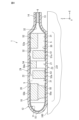
- FIG. 1 is a schematic plan view showing a first embodiment of a stretchable device.
- 2 is a sectional view taken along line II-II in FIG. 1.
- FIG. 2 is a sectional view taken along line II-II in FIG. 1.
- FIG. 2 is a sectional view taken along line II-II in FIG. 1.
- FIG. 3 is an enlarged view including the vicinity of the first electronic component in FIG. 2.
- FIG. 3 is a cross-sectional view of a second embodiment of a stretchable device.
- FIG. 7 is a cross-sectional view of a third embodiment of a stretchable device.
- FIG. 4 is a cross-sectional view of a fourth embodiment of a stretchable device.
- FIG. 1 is a schematic plan view showing a first embodiment of a stretchable device.
- FIG. 2 is a sectional view taken along line II-II in FIG.
- the stretchable device 1 includes a stretchable substrate 10 that can be stretched and contracted, and a plurality of electronic components 51 to 55 provided on the stretchable substrate 10.
- the stretchable device 1 is, for example, attached to the body surface of a living body and used for sensing biological signals, healing, and treatment.
- the stretchable device 1 is a biological interface circuit module having flexibility and stretchability.
- on the stretchable substrate does not refer to an absolute direction such as vertically upward defined by the direction of gravity, but rather to the outside and inside of the stretchable substrate with the surface of the stretchable substrate as the boundary. It refers to the direction towards the outside. Therefore, “on the stretchable substrate” is a relative direction determined by the orientation of the surface of the stretchable substrate. Furthermore, “above” an element does not only mean a position directly above the element (on), but also a position above the element that is away from it, that is, a position above the element through other objects. Also includes spaced above positions.
- the length direction (longitudinal direction) of the stretchable device 1 is assumed to be the X direction.
- the width direction of the stretchable device 1 is defined as the Y direction.
- the thickness direction of the stretchable device 1 is defined as the Z direction.
- the X direction, Y direction, and Z direction are mutually orthogonal directions, and when arranged in the order of X, Y, and Z, form a right-handed system.
- the forward Z direction is also referred to as the upper side of the Z direction
- the reverse Z direction is also referred to as the lower side of the Z direction.
- the stretchable substrate 10 has a first main surface 11 and a second main surface 12.
- the first main surface 11 includes a first region Z1 and a second region Z2.
- the first region Z1 and the second region Z2 are regions where electronic components can be mounted, for example, regions where stretchable wiring connected to the electronic components is provided.
- the stretchable substrate 10 is folded back so that the first main surface 11 is on the inside.
- electronic components may be placed on the first main surface 11.
- the stretchable substrate 10 is folded back so that the first region Z1 and the second region Z2 of the first main surface 11 face each other.
- the electronic component may be placed in at least one of the first region Z1 and the second region Z2.
- the stretchable substrate 10 is folded back so that the first main surface 11 is on the inside, and the electronic components 51 to 55 can be placed on the first main surface 11. Therefore, the plurality of electronic components 51 to 55 are arranged inside the folded stretchable substrate 10. Therefore, the possibility of moisture intruding into the inside of the stretchable substrate 10 can be reduced, and the plurality of electronic components 51 to 55 can be protected from moisture.
- the number of electronic components may be one, and in this case, one electronic component is disposed in at least one of the first region Z1 and the second region Z2, thereby protecting the electronic component from moisture. Can be done.
- the first main surface 11 of the stretchable substrate 10 has a first region Z1 and a second region Z2.
- the first region Z1 is located on the lower side in the Z direction
- the second region Z2 is located on the upper side in the Z direction.
- the first region Z1 and the second region Z2 are each a flat surface and are arranged parallel to each other.
- a flat surface includes not only a completely flat surface but also a substantially flat surface.
- parallel includes not only completely parallel but also substantially parallel.
- at least one of the first region Z1 and the second region Z2 may be bent to some extent. The same applies hereafter.
- the second main surface 12 of the stretchable substrate 10 has a third region Z3 and a fourth region Z4.
- the third region Z3 is located on the opposite side to the first region Z1, and the fourth region Z4 is located on the opposite side to the second region Z2.
- the third region Z3 is located on the lower side in the Z direction, and the fourth region Z4 is located on the upper side in the Z direction.
- the third region Z3 and the fourth region Z4 are each flat surfaces and are arranged parallel to each other.
- the stretchable substrate 10 has a bent portion 15.
- the bent portion 15 extends along the Y direction and is curved to protrude in the reverse X direction.
- a curved apex portion 15a of the bent portion 15 extends in the Y direction.
- the vertex portion 15a is located at the center of the bent portion 15 in the Z direction.
- the stretchable substrate 10 has a first edge portion 13 located on the first region Z1 side and a second edge portion 14 located on the second region Z2 side.
- the first edge portion 13 is a portion located closer to the first region Z1 (third region Z3) than the apex portion 15a of the edge portions around the entire circumference of the stretchable substrate 10.
- the second edge portion 14 is a portion of the peripheral edge portion of the stretchable substrate 10 located closer to the second region Z2 (fourth region Z4) than the apex portion 15a.
- the first edge portion 13 has an end portion 13a facing the apex portion 15a in the X direction, and a side portion 13b located between the apex portion 15a and the end portion 13a.
- the second edge portion 14 has an end portion 14a facing the apex portion 15a in the X direction, and a side portion 14b located between the apex portion 15a and the end portion 14a.
- the end 13a of the first end edge 13 and the end 14a of the second end edge 14 are opposite to each other in the Z direction, and the side 13b of the first end 13 and the side 14b of the second end 14 are opposite to each other in the Z direction. are opposed in the Z direction.
- the electronic components 51 to 55 are surrounded by the first edge portion 13 when viewed from above. Therefore, it is possible to suppress moisture from entering the electronic components 51 to 55 from all sides.
- the connecting member 6 is, for example, an anisotropic conductive adhesive, and has conductivity in the thickness direction and insulation in the planar direction.
- the connecting member 6 includes a thermosetting epoxy resin and conductive particles contained in the resin.
- the first edge portion 13 and at least a portion of the second edge portion 14 are connected to each other via the connecting member 6.
- the possibility of water intrusion can be further reduced.
- the side portion 13b of the first edge portion 13 and the side portion 14b of the second edge portion 14 may be connected via the connecting member 6.
- the stretchable device 1 further includes an elastic member 5 that contacts the first region Z1 and the second region Z2.
- the elastic member 5 is a member having flexibility and elasticity, and is made of, for example, a sponge material such as polyurethane foam or polyester. According to the above configuration, the elastic member 5 is sandwiched between the first region Z1 and the second region Z2 and supports the first region Z1 and the second region Z2, so that strength against external pressure can be ensured.
- the elastic member 5 when the second region Z2 is arranged above the first region Z1 in the direction of gravity, even if the second region Z2 bends under its own weight, the elastic member 5 does not move between the first region Z1 and the second region Z2. Therefore, the second region Z2 can be prevented from coming into contact with the first region Z1.
- the elastic member 5 covers at least a portion of the plurality of electronic components 51 to 55. Thereby, the elastic member 5 can absorb external impact and protect the plurality of electronic components 51 to 55. Further, the elastic member 5 can suppress the infiltration of moisture and protect the plurality of electronic components 51 to 55 from moisture.
- the stretchable substrate 10 includes a stretchable base material 20 that is stretchable and a stretchable wire 30 that is provided on the stretchable base material 20.
- the first main surface 11 includes the surface of the main surface of the stretchable base material 20 that is exposed from the stretchable wiring 30, and the upper surface of the stretchable wire 30 on the opposite side to the lower surface that contacts the stretchable base material 20. It consists of The same applies to the first region Z1 and the second region Z2. Note that the stretchable substrate 10 does not need to have the stretchable wiring 30.
- the first main surface 11 is constituted by the main surface of the stretchable base material 20.
- the stretchable base material 20 is a sheet-like or film-like base material made of a stretchable resin material, and is folded back in two.
- the resin material is, for example, styrene resin, olefin resin, epoxy resin, urethane resin, acrylic resin, or silicone resin, preferably urethane resin.
- the urethane resin include thermoplastic polyurethane.
- the styrene resin include styrene-butadiene-styrene copolymer resin.
- the stretch rate of the stretchable base material 20 is preferably 50% or more. By setting the stretch ratio as described above, the stretchable device 1 can better follow the living body.
- the Young's modulus of the stretchable base material 20 is preferably 100 MPa or less, more preferably 30 MPa or less. By setting the Young's modulus as described above, the user's discomfort can be suppressed.
- the water absorption rate of the stretchable base material 20 is preferably 1% by weight or less from the viewpoint of more reliably ensuring the reliability of the stretchable device 1.
- the thickness of the stretchable base material 20 is, for example, 0.1 ⁇ m or more and 100 ⁇ m or less.
- the width of the stretchable base material 20 is, for example, 10 mm or more and 100 mm or less.
- the stretchable wiring 30 extends along the main surface of the stretchable base material 20.
- the stretchable wiring 30 may extend not only in one direction on the XY plane, but also while bending in a plurality of directions on the XY plane.
- the stretchable wiring 30 may be embedded in the stretchable base material 20 such that a part of the stretchable wire 30 is exposed from the main surface of the stretchable base material 20.
- the stretchable wiring 30 is made of a stretchable conductive material.
- metal foil such as silver, copper, or nickel may be used as the conductive material, or metal powder such as silver, copper, or nickel and elastomeric resin such as epoxy resin, urethane resin, acrylic resin, or silicone resin may be used.
- the metal powder is preferably silver. Thereby, the stretchable wiring 30 with low resistance can be formed.
- the average particle D50 of the metal powder is preferably 0.01 ⁇ m or more and 10 ⁇ m or less.
- the shape of the metal powder may be spherical, flat, irregularly shaped with protrusions, etc.
- the thickness of the stretchable wiring 30 is preferably 100 ⁇ m or less, more preferably 50 ⁇ m or less, and preferably 1 ⁇ m or more, more preferably 10 ⁇ m or more.
- the width of the stretchable wiring 30 is preferably 0.2 mm or more.
- the stretchable wiring 30 is formed by screen printing, inkjet printing, dispensing, etc. so as to be in direct contact with the main surface of the stretchable base material 20. Note that the stretchable wiring 30 may be arranged on the main surface of the stretchable base material 20 with an insulating protective film (not shown) interposed therebetween.
- the stretchable wiring 30 has a first wiring part 31 provided on the first region Z1 side and a second wiring part 32 provided on the second region Z2 side.
- the first wiring portion 31 is a portion of the stretchable wiring 30 located closer to the first region Z1 than the vertex portion 15a.
- the second wiring portion 32 is a portion of the stretchable wiring 30 located closer to the second region Z2 than the vertex portion 15a.
- the first wiring section 31 and the second wiring section 32 are electrically connected. Specifically, the first wiring section 31 and the second wiring section 32 are connected via the connecting member 6 on the end portions 13a and 14a side. On the other hand, on the bending part 15 side, the first wiring part 31 and the second wiring part 32 are directly connected. Note that the first wiring portion 31 and the second wiring portion 32 may be electrically connected at one of the end portions 13a and 14a side or the bent portion 15 side.
- the connecting member 6 can be used to electrically connect the first wiring part 31 and the second wiring part 32, and to connect the first edge part 13 and the second end. It can also be used for the physical connection of the edge 14.
- the plurality of electronic components 51 to 55 include a first electronic component 51, a second electronic component 52, a third electronic component 53, a fourth electronic component 54, and a fifth electronic component 55.
- the first electronic component 51 is a temperature sensor that measures the temperature of a living body.
- the second electronic component 52 is a BLE module that includes an antenna and wirelessly communicates signals.
- the third electronic component 53 is an acceleration sensor that measures the acceleration of a living body.
- the fourth electronic component 54 is an LED that measures SpO2 (percutaneous arterial oxygen saturation).
- the fifth electronic component 55 is a battery that serves as a power source for operating the circuit. Note that it may also include other electronic components such as a coil that irradiates electromagnetic waves into the body, an ultrasonic oscillator that irradiates ultrasonic waves into the body, and a light receiving sensor.
- the plurality of electronic components 51 to 55 are arranged in both the first region Z1 and the second region Z2. That is, the first electronic component 51 is arranged in the first region Z1, and the second electronic component 52 is arranged in the second region Z2.
- the first electronic component 51 is arranged in the first region Z1
- the second electronic component 52 is arranged in the second region Z2.
- the portion of the stretchable substrate 10 where the electronic components are installed is compared to the portion of the stretchable substrate 10 where no electronic components are installed. It becomes hard.
- the second main surface of the stretchable board is placed on the human body surface in a state where the stretchable board is unfolded without being folded back as in the past, the user may I feel discomfort due to the hardness. Particularly in areas where electronic components are mounted at a high density, the impact on the user is significant.
- the size of the stretchable substrate is increased in order to lower the mounting density of electronic components, there is a problem in that the dead space on the first main surface of the stretchable substrate increases. Furthermore, if the stretchable substrate is made larger, the locations on the human body to which it can be attached will be limited.
- a plurality of electronic components can also be provided in the second region Z2 on the back side of the fourth region Z4 on the side that does not come into contact with the human body. Even if the mounting density of electronic components on the first main surface 11 is increased and the dead space on the first main surface 11 of the stretchable substrate 10 is reduced, the user's discomfort can be reduced. For example, a small-sized electronic component can be placed on the first region Z1 side, and a large-sized electronic component can be placed on the second region Z2 side.
- the stretchable substrate 10 since the stretchable substrate 10 is used by being bent, the area of the contact surface of the stretchable substrate 10 that comes into contact with the body surface is reduced, reducing discomfort for the user, and it also stretches and contracts according to the location on the human body to which it is attached. The size of the sexual substrate can be adjusted.
- the third electronic component 53 is arranged in the first region Z1
- the fourth electronic component 54 is arranged in the second region Z2. According to the above configuration, even if the mounting density of electronic components is increased and the dead space on the first main surface 11 of the stretchable substrate 10 is reduced, the user's discomfort can be reduced.
- the fifth electronic component 55 is arranged so as to contact both the first region Z1 and the second region Z2.
- the first electronic component 51, the second electronic component 52, the third electronic component 53, the fourth electronic component 54, and the fifth electronic component 55 are each connected to the stretchable wiring 30. Specifically, the first electronic component 51, the third electronic component 53, and the fifth electronic component 55 are each connected to the first wiring section 31. The second electronic component 52, the fourth electronic component 54, and the fifth electronic component 55 are each connected to the second wiring section 32.
- the first electronic component 51 and the third electronic component 53 are body surface close type electronic components.
- a body surface close type electronic component is an electronic component that is preferably placed close to the body surface.
- the temperature sensor (first electronic component 51) and acceleration sensor (third electronic component 53) are preferably mounted close to the body surface in order to measure highly accurate data.
- the second electronic component 52 and the fourth electronic component 54 are body surface-separated electronic components.
- a body surface-separated type electronic component is an electronic component that is preferably placed away from the body surface. Specifically, since the LED (second electronic component 52) has a light emitting part on the top surface of the component, it is necessary to mount the LED (second electronic component 52) on the side opposite to the body surface so that the top surface of the component is on the body surface side. Since the BLE module (fourth electronic component 54) has the property that the human body absorbs radio waves, the communication state can be improved if the BLE module (fourth electronic component 54) is mounted at a position as far away from the human skin as possible.
- the first electronic component 51 and The third electronic component 53 is placed on the side closer to the body surface, and the second electronic component 52 and the fourth electronic component 54 are placed on the side farther from the body surface.
- the first electronic component 51 and the second electronic component 52 do not overlap in the direction perpendicular to the first region Z1.
- the direction perpendicular to the first region Z1 corresponds to the Z direction.
- the first electronic component 51 and the second electronic component 52 do not interfere with each other in the direction perpendicular to the first region Z1. Thereby, the thickness of the stretchable device 1 can be reduced so that the first region Z1 and the second region Z2 are brought closer to each other.
- the first electronic component 51 and the fourth electronic component 54 do not overlap in the direction perpendicular to the first region Z1.
- the second electronic component 52 and the third electronic component 53 do not overlap in the direction perpendicular to the first region Z1.
- the third electronic component 53 and the fourth electronic component 54 do not overlap in the direction perpendicular to the first region Z1.
- the fifth electronic component 55 does not overlap with the first to fourth electronic components 51 to 54 in the direction orthogonal to the first region Z1.
- the electronic components may overlap when viewed from the direction orthogonal to the first region Z1, and in this case, the planar area of the stretchable base material 20 when viewed from the direction orthogonal to the first region Z1 can be further reduced.
- the elastic member 5 between the upper and lower electronic components, interference between the upper and lower electronic components can be suppressed.
- the first electronic component 51 and the second electronic component 52 overlap in the direction parallel to the first region Z1.
- the direction orthogonal to the first region Z1 corresponds to the XY plane direction.
- the first electronic component 51 and the second electronic component 52 can be arranged so as not to interfere with each other in the direction orthogonal to the first region Z1. Thereby, the thickness of the stretchable device 1 can be reduced so that the first region Z1 and the second region Z2 are brought closer to each other.
- the first electronic component 51 and the fourth electronic component 54 overlap in the direction parallel to the first region Z1.
- the second electronic component 52 and the third electronic component 53 overlap in a direction parallel to the first region Z1.
- the third electronic component 53 and the fourth electronic component 54 overlap in a direction parallel to the first region Z1.
- the fifth electronic component 55 overlaps with the first to fourth electronic components 51 to 54 in the direction parallel to the first region Z1. Note that the electronic components do not need to overlap in the direction parallel to the first region Z1.
- FIG. 3 is a cross-sectional view taken along line II-II in FIG. 1.
- the sum of the first thickness T1 of the first electronic component 51 and the second thickness T2 of the second electronic component 52 is greater than the longest distance L between the first region Z1 and the second region Z2. It's also big.
- the thickness refers to the size in the direction orthogonal to the first region Z1, and the longest distance refers to the longest size in the direction orthogonal to the first region Z1.
- the first electronic component 51 and the second electronic component 52 can be arranged so as not to interfere with each other in the direction orthogonal to the first region Z1. Thereby, the thickness of the stretchable device 1 can be reduced so that the first region Z1 and the second region Z2 are brought closer to each other.
- the sum of the first thickness T1 of the first electronic component 51 and the fourth thickness T4 of the fourth electronic component 54 is greater than the longest distance L.
- the sum of the second thickness T2 of the second electronic component 52 and the third thickness T3 of the third electronic component 53 is greater than the longest distance L.
- the sum of the third thickness T3 of the third electronic component 53 and the fourth thickness T4 of the fourth electronic component 54 is greater than the longest distance L. Note that the total thickness of a pair of upper and lower electronic components may be smaller than the longest distance.
- FIG. 4 is a cross-sectional view taken along line II-II in FIG. 1.
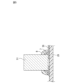
- the third region Z3 of the second main surface 12 of the stretchable substrate 10 has a body surface region Z31 that can be brought into contact with the body surface 100.
- body surface 100 represents the skin of a human body.
- the total area of the installation surfaces of the plurality of electronic components 51 to 55 installed in the first region Z1 and the second region Z2 is larger than the area of the body surface region Z31.
- the installation surface is not limited to a surface that directly contacts the stretchable substrate 10, but is a surface that faces the stretchable substrate 10 when installed on the stretchable substrate 10.
- the installation surface 51a of the first electronic component 51 is a surface facing the first region Z1.
- the installation surface 52a of the second electronic component 52 is a surface facing the second region Z2.
- the installation surface 53a of the third electronic component 53 is a surface facing the first region Z1.
- the installation surface 54a of the fourth electronic component 54 is a surface facing the second region Z2.
- the first installation surface 55a of the fifth electronic component 55 is a surface facing the first region Z1
- the second installation surface 55b of the fifth electronic component 55 is a surface facing the second region Z2.
- the total area of each of the installation surfaces 51a, 52a, 53a, 54a, 55a, and 55b is larger than the area of the body surface region Z31.
- FIG. 5 is an enlarged view including the vicinity of the first electronic component 51 in FIG. 2.
- the first electronic component 51 is connected to the stretchable wiring 30 via the joint 7 .
- the joint portion 7 is made of, for example, a conductive member such as solder.
- the joint portion 7 is covered with a covering portion 8 .
- the covering portion 8 is made of a resin such as a thermosetting epoxy resin, for example. Thereby, the joint portion 7 can be protected from mechanical stress due to expansion and contraction of the stretchable substrate 10 (stretchable base material 20 and stretchable wiring 30).
- the stretchable substrate 10 is developed into a sheet shape, and a plurality of electronic components 51 to 55 are installed in each of the first region Z1 and the second region Z2 of the first main surface 11 of the stretchable substrate 10. Furthermore, the elastic member 5 is provided in at least one of the first region Z1 and the second region Z2.
- the stretchable substrate 10 is folded in half so that the first main surface 11 is on the inside.
- the stretchable substrate 10 is folded back so that the first region Z1 and the second region Z2 face each other.
- the electronic components 51 and 53 installed in the first region Z1 and the electronic components 52 and 54 installed in the second region Z2 do not interfere with each other in the direction perpendicular to the first region Z1.
- FIG. 6 is a cross-sectional view of a second embodiment of a stretchable device.
- FIG. 6 is a diagram corresponding to the II-II cross section in FIG.
- the second embodiment differs from the first embodiment in that no connecting member is provided. This different configuration will be explained below.
- the other configurations are the same as those in the first embodiment, are given the same reference numerals as in the first embodiment, and the description thereof will be omitted.
- the elastic device 1A of the second embodiment does not include the connecting member 6 of the first embodiment. That is, the first edge part 13 and the second edge part 14 are not connected and are separated from each other. Specifically, the end 13a of the first end 13 and the end 14a of the second end 14 are separated from each other.
- the elastic member 5 may not be further provided.
- the connecting member 6 may be provided without providing the elastic member 5.
- FIG. 7 is a cross-sectional view of a third embodiment of a stretchable device.
- FIG. 7 is a diagram corresponding to the II-II cross section in FIG.
- the third embodiment differs from the first embodiment in the number of electronic components. This different configuration will be explained below.
- the other configurations are the same as those in the first embodiment, are given the same reference numerals as in the first embodiment, and the description thereof will be omitted.
- the stretchable device 1B of the third embodiment there is one electronic component, and it is arranged in at least one of the first region Z1 and the second region Z2. Specifically, the first electronic component 51 is arranged in the first region Z1. Note that the first electronic component 51 may be any of the electronic components shown as examples of the electronic components 51 to 55 in paragraph [0036].
- the first electronic component 51 is placed inside the folded stretchable substrate 10. Therefore, the possibility of moisture intruding into the inside of the stretchable substrate 10 can be reduced, and the first electronic component 51 can be protected from moisture.
- one electronic component may be placed in the second area Z2 instead of the first area Z1, or may be placed in contact with both the first area Z1 and the second area Z2.
- FIG. 8 is a cross-sectional view of a fourth embodiment of a stretchable device.
- FIG. 8 is a diagram corresponding to the II-II cross section in FIG.
- the fourth embodiment differs from the first embodiment in that it is composed of multiple types of base materials. This different configuration will be explained below.
- the other configurations are the same as those in the first embodiment, are given the same reference numerals as in the first embodiment, and the description thereof will be omitted.
- the stretchable base material 20 in the first embodiment has a configuration in which it is folded back in two as a whole.
- the stretchable base material 20 having the folded structure has a single shape or one type of continuous shape.
- a plurality of types of base materials take a continuous form, and as a whole, a stretchable composite base material with a folded structure can be configured.
- a first elastic base material 21 and a second base material 22 made of different materials are connected so as to be in contact with each other in the longitudinal direction.
- the second base material 22 is located in a relatively upper part of the stretchable composite base material with a folded structure, and most of the first stretchable base material 21 is located at the bottom. It is located on the side and both are continuous.
- the second base material 22 when the second base material 22 does not include a curved portion due to folding, the second base material 22 may be a base material that does not have elasticity. Specific examples include rigid substrates and FPCs. Moreover, it goes without saying that the second base material may have elasticity. When the second base material has stretchability, the second base material may include a curved portion.
- the first stretchable base material 21 and the second base material 22 may be made of the same material as the stretchable base material 20 described in the section of the first embodiment. Something can happen.
- the material of the first elastic base material 21 may be one type of resin material selected from the group consisting of styrene resin, olefin resin, epoxy resin, urethane resin, acrylic resin, and silicone resin, and
- the material of the base material 22 (if it has stretchability) may be a different material from the material used for the first stretchable base material.
- a stretchable stretchable substrate having a first main surface and a second main surface; and an electronic component provided on the stretchable substrate,
- the first main surface includes a first region and a second region,
- the stretchable substrate is folded back so that the first main surface is on the inside and the first region and the second region are opposite to each other,
- the electronic component is a stretchable device arranged in at least one of the first region and the second region.
- the stretchable substrate has a first edge portion located on the first region side and a second edge portion located on the second region side, and at least a portion of the first edge portion and a second edge portion located on the second region side.
- the stretchable substrate has a stretchable stretchable base material and stretchable stretchable wiring provided on the stretchable base material,
- the stretchable wiring has a first wiring part provided on the first region side and a second wiring part provided on the second region side,
- the stretchable device according to any one of ⁇ 1> to ⁇ 3>, wherein the first wiring part and the second wiring part are electrically connected.
- the elastic device according to any one of ⁇ 1> to ⁇ 4>, further comprising an elastic member that contacts the first region and the second region.
- a plurality of electronic components exist, The plurality of electronic components include a first electronic component and a second electronic component, The stretchable device according to any one of ⁇ 1> to ⁇ 5>, wherein the first electronic component is arranged in the first region, and the second electronic component is arranged in the second region.
- the first electronic component is a body surface close type electronic component
- the stretchable device according to ⁇ 6>, wherein the second electronic component is a body surface-separated electronic component.
- ⁇ 8> The stretchable device according to ⁇ 6> or ⁇ 7>, wherein the first electronic component and the second electronic component do not overlap in a direction perpendicular to the first region.
- ⁇ 9> Any one of ⁇ 6> to ⁇ 8>, wherein the sum of the thickness of the first electronic component and the thickness of the second electronic component is greater than the longest distance between the first region and the second region.
- the stretchable device described in . ⁇ 10> The stretchable device according to any one of ⁇ 6> to ⁇ 9>, wherein the first electronic component and the second electronic component overlap in a direction parallel to the first region.
- a plurality of electronic components exist, The plurality of electronic components are arranged in both the first region and the second region, The second main surface has a third region opposite to the first region, and the third region has a body surface region that can be contacted with the body surface, The total area of the installation surfaces of the plurality of electronic components installed in the first region and the second region is larger than the area of the body surface region, and the total area is one of ⁇ 1> to ⁇ 3>. Stretchable device as described.
Landscapes
- Engineering & Computer Science (AREA)
- Microelectronics & Electronic Packaging (AREA)
- Structure Of Printed Boards (AREA)
Abstract
本開示の伸縮性デバイスは、第1主面および第2主面を有する伸縮可能な伸縮性基板と、前記伸縮性基板上に設けられた電子部品とを備え、前記第1主面は、第1領域と第2領域を含み、前記伸縮性基板は、前記第1主面が内側となるように、折り返されており、前記電子部品は、前記第1主面に配置される。
Description
本開示は、伸縮性デバイスに関する。
従来、伸縮性デバイスとしては、WO2014/203586号公報(特許文献1)に記載されたものがある。この伸縮性デバイスは、主面を有する伸縮性基板と、伸縮性基板上に設けられた電子部品とを備える。
ところで、前記従来のような伸縮性デバイスは、例えば、生体の体表に貼り付けられて、生体信号のセンシングや、癒し、治療を行う用途に使用される。このとき、汗やシャワーなどの水分が電子部品内に浸入し、電子部品が損傷するおそれがある。
そこで、本開示の目的は、電子部品を水分から保護することができる伸縮性デバイスを提供することにある。
前記課題を解決するため、本開示の一態様である伸縮性デバイスは、
第1主面および第2主面を有する伸縮可能な伸縮性基板と、
前記伸縮性基板上に設けられた電子部品と
を備え、
前記第1主面は、第1領域と第2領域を含み、
前記伸縮性基板は、前記第1主面が内側となるように、折り返されており、
前記電子部品は、前記第1主面に配置される。
第1主面および第2主面を有する伸縮可能な伸縮性基板と、
前記伸縮性基板上に設けられた電子部品と
を備え、
前記第1主面は、第1領域と第2領域を含み、
前記伸縮性基板は、前記第1主面が内側となるように、折り返されており、
前記電子部品は、前記第1主面に配置される。
前記態様によれば、伸縮性基板は、第1主面が内側となるように折り返されるので、電子部品は、折り返された伸縮性基板の内側に配置されることになる。このため、伸縮性基板の内側への水分の浸入の可能性を低減でき、電子部品を水分から保護することができる。
本開示の一態様である伸縮性デバイスによれば、電子部品を水分から保護することができる。
以下、本発明の実施形態について、図面を用いて詳細に説明する。各々の実施形態では、その実施形態以前に説明した点と異なる点について主に説明する。特に、同様の構成による同様の作用効果については実施形態ごとには逐次言及しない。以下の実施形態における構成要素のうち、独立請求項に記載されていない構成要素については、任意の構成要素として説明される。また、図面に示される構成要素の大きさおよび大きさの比は、必ずしも厳密ではない。また、各図において、実質的に同一の構成に対しては同一の符号を付しており、重複する説明は省略又は簡略化する場合がある。
<第1実施形態>
[伸縮性デバイス1の概略構成]
図1は、伸縮性デバイスの第1実施形態を示す概略平面図である。図2は、図1のII-II断面図である。図1と図2に示すように、伸縮性デバイス1は、伸縮可能な伸縮性基板10と、伸縮性基板10上に設けられた複数の電子部品51~55とを備える。伸縮性デバイス1は、例えば、生体の体表に貼り付けられて、生体信号のセンシングや、癒し、治療を行う用途に使用される。つまり、伸縮性デバイス1は、柔軟性、伸縮性を備えた生体インタフェース回路モジュールである。
[伸縮性デバイス1の概略構成]
図1は、伸縮性デバイスの第1実施形態を示す概略平面図である。図2は、図1のII-II断面図である。図1と図2に示すように、伸縮性デバイス1は、伸縮可能な伸縮性基板10と、伸縮性基板10上に設けられた複数の電子部品51~55とを備える。伸縮性デバイス1は、例えば、生体の体表に貼り付けられて、生体信号のセンシングや、癒し、治療を行う用途に使用される。つまり、伸縮性デバイス1は、柔軟性、伸縮性を備えた生体インタフェース回路モジュールである。
ここで、「伸縮性基板上」とは、重力方向に規定される鉛直上方のような絶対的な一方向ではなく、当該伸縮性基板の表面を境界とする伸縮性基板の外側と内側とのうち、外側に向かう方向を指す。したがって、「伸縮性基板上」とは伸縮性基板の表面の向きによって定まる相対的な方向である。また、ある要素に対して「上」には、当該要素と接する直上の位置(on)だけではなく、当該要素とは離れた上方、すなわち当該要素上の他の物体を介した上側の位置や間隔を空けた上側の位置(above)も含む。
図面に示すように、以下では、説明の便宜上、伸縮性デバイス1の長さ方向(長手方向)をX方向とする。伸縮性デバイス1の幅方向をY方向とする。伸縮性デバイス1の厚さ方向をZ方向とする。X方向、Y方向及びZ方向は、互いに直交する方向であって、X、Y、Zの順に並べたとき、右手系を構成する。順Z方向をZ方向上側ともいい、逆Z方向をZ方向下側ともいう。
伸縮性基板10は、第1主面11および第2主面12を有する。第1主面11は、第1領域Z1と第2領域Z2を含む。第1領域Z1および第2領域Z2は、それぞれ、電子部品が実装され得る領域であり、例えば、電子部品に接続される伸縮性配線が設けられた領域である。
伸縮性基板10は、第1主面11が内側となるように折り返されている。この場合において、電子部品は第1主面11に配置され得る。一例では、第1主面11が内側に位置づけられることを前提として、第1主面11の第1領域Z1と第2領域Z2が対向するように、伸縮性基板10は折り返される。この場合において、電子部品は、第1領域Z1と第2領域Z2の少なくとも一方に配置され得る。
上記構成によれば、伸縮性基板10は第1主面11が内側となるように折り返され、かつ電子部品51~55は第1主面11に配置され得る。そのため、複数の電子部品51~55は、折り返された伸縮性基板10の内側に配置されることになる。このため、伸縮性基板10の内側への水分の浸入の可能性を低減でき、複数の電子部品51~55を水分から保護することができる。なお、電子部品は、1つであってもよく、このとき、1つの電子部品は、第1領域Z1と第2領域Z2の少なくとも一方に配置され、これより、電子部品を水分から保護することができる。
また、伸縮性基板を展開した状態で使用する場合、伸縮性基板の主面に配置された電子部品を水分から保護するために電子部品の全体を樹脂モールドでの封止が必要となる。そのような場合と比較して、電子部品が伸縮性基板10の内側に配置されることで、樹脂モールドを設けるための製造工程や製造コストが不要になる。
[伸縮性デバイス1の詳細構成]
伸縮性基板10の第1主面11は、第1領域Z1と第2領域Z2とを有する。第1領域Z1は、Z方向下側に位置し、第2領域Z2は、Z方向上側に位置する。第1領域Z1および第2領域Z2は、それぞれ、平坦面であり、互いに平行に配置される。
ここで、平坦面とは、完全に平坦な面である場合のみならず、実質的に平坦な面である場合を含む。例えば、第1領域Z1および第2領域Z2に配線を含む場合、配線の凸形状は許容される。また、平行とは、完全に平行である場合のみならず、実質的に平行である場合を含む。例えば、第1領域Z1および第2領域Z2の少なくとも一方は、多少撓んでいてもよい。以下、同様である。
伸縮性基板10の第1主面11は、第1領域Z1と第2領域Z2とを有する。第1領域Z1は、Z方向下側に位置し、第2領域Z2は、Z方向上側に位置する。第1領域Z1および第2領域Z2は、それぞれ、平坦面であり、互いに平行に配置される。
ここで、平坦面とは、完全に平坦な面である場合のみならず、実質的に平坦な面である場合を含む。例えば、第1領域Z1および第2領域Z2に配線を含む場合、配線の凸形状は許容される。また、平行とは、完全に平行である場合のみならず、実質的に平行である場合を含む。例えば、第1領域Z1および第2領域Z2の少なくとも一方は、多少撓んでいてもよい。以下、同様である。
伸縮性基板10の第2主面12は、第3領域Z3と第4領域Z4とを有する。第3領域Z3は、第1領域Z1と反対側に位置し、第4領域Z4は、第2領域Z2と反対側に位置する。第3領域Z3は、Z方向下側に位置し、第4領域Z4は、Z方向上側に位置する。第3領域Z3および第4領域Z4は、それぞれ、平坦面であり、互いに平行に配置される。
伸縮性基板10は、折り曲げられた折曲部15を有する。折曲部15は、Y方向に沿って延在し、逆X方向に突出するように湾曲している。折曲部15の湾曲の頂点部分15aは、Y方向に延在している。頂点部分15aは、折曲部15のZ方向の中央に位置する。
伸縮性基板10は、第1領域Z1側に位置する第1端縁部13と、第2領域Z2側に位置する第2端縁部14とを有する。第1端縁部13は、伸縮性基板10の全周の端縁部のうちの頂点部分15aよりも第1領域Z1(第3領域Z3)側に位置する部分である。第2端縁部14は、伸縮性基板10の周縁部のうちの頂点部分15aよりも第2領域Z2(第4領域Z4)側に位置する部分である。
第1端縁部13は、頂点部分15aのX方向に対向する端部13aと、頂点部分15aと端部13aとの間に位置する側部13bとを有する。第2端縁部14は、頂点部分15aのX方向に対向する端部14aと、頂点部分15aと端部14aとの間に位置する側部14bとを有する。第1端縁部13の端部13aと第2端縁部14の端部14aは、Z方向に対向し、第1端縁部13の側部13bと第2端縁部14の側部14bは、Z方向に対向する。言い換えれば、上面視において、電子部品51~55の周囲は、第1端縁部13によって囲まれている。したがって、電子部品51~55への四方からの水分の侵入を抑制することができる。
第1端縁部13の少なくとも一部と第2端縁部14の少なくとも一部とは、接続部材6を介して、接続されている。具体的に述べると、第1端縁部13の端部13aと第2端縁部14の端部14aは、接続部材6を介して、接続されている。接続部材6は、例えば、異方性導電接着剤であり、厚さ方向に対して導通性を有し、面方向に対しては絶縁性を有する。接続部材6は、熱硬化性のエポキシ樹脂と樹脂に含有される導電性粒子とを含む。
上記構成によれば、第1端縁部13の少なくとも一部と第2端縁部14の少なくとも一部とは、接続部材6を介して、接続されているので、伸縮性基板10の内側への水分の浸入の可能性をより低減できる。なお、第1端縁部13の側部13bと第2端縁部14の側部14bは、接続部材6を介して、接続されていてもよい。
伸縮性デバイス1は、さらに、第1領域Z1および第2領域Z2に接触する弾性部材5を有する。弾性部材5は、柔軟性や弾性を有する部材であり、例えば、ポリウレタンフォームやポリエステルなどのスポンジ材からなる。上記構成によれば、弾性部材5は、第1領域Z1と第2領域Z2に挟まれて第1領域Z1と第2領域Z2を支持するので、外部からの圧力に対する強度を確保できる。また、第2領域Z2を第1領域Z1よりも重力方向の上側に配置する場合、第2領域Z2が自重で撓んだとしても、弾性部材5が第1領域Z1と第2領域Z2の間に存在しているので、第2領域Z2が第1領域Z1に接触することを防止できる。
弾性部材5は、複数の電子部品51~55の少なくとも一部を覆っている。これにより、弾性部材5は外部からの衝撃を吸収して、複数の電子部品51~55を保護することができる。また、弾性部材5は水分の浸入を抑制して、複数の電子部品51~55を水分から保護することができる。
伸縮性基板10は、伸縮可能な伸縮性基材20と、伸縮性基材20に設けられた伸縮可能な伸縮性配線30とを有する。このとき、第1主面11は、伸縮性基材20の主面のうちの伸縮性配線30から露出する面と、伸縮性配線30の伸縮性基材20に接触する下面と反対側の上面とから構成される。第1領域Z1および第2領域Z2についても同様である。なお、伸縮性基板10は、伸縮性配線30を有していなくてもよい。このとき、第1主面11は、伸縮性基材20の主面から構成される。
伸縮性基材20は、伸縮性を有する樹脂材料から構成されるシート状あるいはフィルム状の基材であり、2つ折りに折り返されている。樹脂材料としては、例えば、スチレン樹脂、オレフィン樹脂、エポキシ樹脂、ウレタン樹脂、アクリル樹脂又はシリコーン樹脂で形成され、好ましくはウレタン樹脂で形成される。ウレタン樹脂としては、熱可塑性ポリウレタンが挙げられる。スチレン樹脂としては、スチレン-ブタジエン-スチレン共重合樹脂が挙げられる。
伸縮性基材20の伸縮率は、50%以上であることが好ましい。前記伸縮率とすることで、伸縮性デバイス1の生体への追従性が良好になる。伸縮性基材20のヤング率は、好ましくは100MPa以下であり、より好ましくは30MPa以下である。前記ヤング率とすることで、使用者の不快感を抑制できる。伸縮性基材20の吸水率は、伸縮性デバイス1の信頼性をより確実に確保する観点から、1重量%以下であることが好ましい。伸縮性基材20の厚さは、例えば、0.1μm以上100μm以下である。伸縮性基材20の幅は、例えば、10mm以上100mm以下である。
伸縮性配線30は、伸縮性基材20の主面上に沿って延在する。伸縮性配線30は、XY平面の一方向のみならず、XY平面の複数の方向に曲がりながら延在してもよい。伸縮性配線30は、複数存在する。伸縮性配線30は、伸縮性配線30の一部が伸縮性基材20の主面から露出するように、伸縮性基材20に埋め込まれていてもよい。伸縮性配線30は、伸縮性を有する導電性材料で形成される。導電性材料には、例えば、銀、銅、ニッケルなどの金属箔を用いてもよく、銀、銅、ニッケルなどの金属粉とエポキシ樹脂、ウレタン樹脂、アクリル樹脂およびシリコーン樹脂などのエラストマ系樹脂とからなる混合物を用いてもよい。金属粉は、銀が好ましい。これにより、低抵抗な伸縮性配線30を形成することができる。金属粉の平均粒子D50は、好ましくは0.01μm以上10μm以下である。金属粉の形状は、球状、扁平状、突起等を有する異形状等であってよい。
伸縮性配線30の厚さは、好ましくは100μm以下、より好ましくは50μm以下であり、好ましくは1μm以上、より好ましくは10μm以上である。伸縮性配線30の厚さが薄いほど、凹凸が小さくラミネート等が容易である。伸縮性配線30の幅は、好ましくは0.2mm以上である。
伸縮性配線30は、伸縮性基材20の主面に直接接触するようにスクリーン印刷、インクジェット印刷、ディスペンスなどにより形成される。なお、伸縮性配線30は、伸縮性基材20の主面上に図示しない絶縁性を有する保護膜を介して配置されていてもよい。
伸縮性配線30は、第1領域Z1側に設けられた第1配線部31と、第2領域Z2側に設けられた第2配線部32とを有する。第1配線部31は、伸縮性配線30のうちの頂点部分15aよりも第1領域Z1側に位置する部分である。第2配線部32は、伸縮性配線30のうちの頂点部分15aよりも第2領域Z2側に位置する部分である。
第1配線部31と第2配線部32は、電気的に接続されている。具体的に述べると、端部13a,14a側において、第1配線部31と第2配線部32は、接続部材6を介して接続されている。一方、折曲部15側において、第1配線部31と第2配線部32は、直接に接続されている。なお、第1配線部31と第2配線部32は、端部13a,14a側または折曲部15側の一方において、電気的に接続されていればよい。
上記構成によれば、第1配線部31と第2配線部32は、電気的に接続されているので、多層基板のようなより複雑な回路パターンを構成できる。また、接続部材6として異方性導電接着剤を用いることで、接続部材6は、第1配線部31と第2配線部32の電気的な接続と、第1端縁部13と第2端縁部14の物理的な接続とを兼用できる。
複数の電子部品51~55は、第1電子部品51と第2電子部品52と第3電子部品53と第4電子部品54と第5電子部品55とを含む。第1電子部品51は、生体の温度を測定する温度センサである。第2電子部品52は、アンテナを含み信号を無線通信するBLEモジュールである。第3電子部品53は、生体の加速度を測定する加速度センサである。第4電子部品54は、SpO2(経皮的動脈血酸素飽和度)を測定するLEDである。第5電子部品55は、回路を動作する電力源となる電池である。なお、体内に電磁波を照射するコイルや、体内に超音波を照射する超音波発振器や、受光センサなどの他の電子部品を含んでいてもよい。
複数の電子部品51~55は、第1領域Z1と第2領域Z2の両方に配置される。つまり、第1電子部品51は、第1領域Z1に配置され、第2電子部品52は、第2領域Z2に配置される。上記構成によれば、伸縮性基板10の第2主面12のうちの第1領域Z1と反対側の第3領域Z3を人間の体表に貼り付けて使用する際、第1電子部品51は、第1領域Z1に配置され、第2電子部品52は、第2領域Z2に配置されるので、使用者は、第2電子部品52の設置に起因する硬さによる不快を感じない。したがって、電子部品の実装密度を高くし、伸縮性基板10の第1主面11におけるデッドスペースを小さくしても、使用者の不快感を低減できる。
ここで、伸縮性基板10の第1主面11に複数の電子部品を配置すると、伸縮性基板10において電子部品を設置した部分が、伸縮性基板10において電子部品を設置していない部分に比べて硬くなる。そして、従来のように、伸縮性基板を折り返さないで展開した状態で、伸縮性基板の第2主面を人間の体表に設置して使用する際、使用者は、電子部品の設置に起因する硬さによる不快を感じる。特に電子部品の実装密度が高い部分では、使用者への影響が大きくなる。一方、電子部品の実装密度を低くするために伸縮性基板のサイズを大きくすると、伸縮性基板の第1主面におけるデッドスペースが大きくなるという問題があった。また、伸縮性基板を大きくすると、人体の貼り付ける箇所が制限されてしまう。
これに対して、本実施形態では、伸縮性基板10を折り曲げて使用することで、人体に接触しない側の第4領域Z4の裏側の第2領域Z2にも複数の電子部品を設けることができ、電子部品の第1主面11に対する実装密度を高くし、伸縮性基板10の第1主面11におけるデッドスペースを小さくしても、使用者の不快感を低減できる。例えば、第1領域Z1側に小さいサイズの電子部品を配置し、第2領域Z2側に大きいサイズの電子部品を配置することができる。また、伸縮性基板10を折り曲げて使用するため、体表に接触する伸縮性基板10の接触面の面積が小さくなり、使用者の不快感を低減できるとともに、人体の貼り付ける箇所に併せて伸縮性基板のサイズを調整できる。
同様に、第3電子部品53は、第1領域Z1に配置され、第4電子部品54は、第2領域Z2に配置される。上記構成によれば、電子部品の実装密度を高くし、伸縮性基板10の第1主面11におけるデッドスペースを小さくしても、使用者の不快感を低減できる。第5電子部品55は、第1領域Z1および第2領域Z2の両方に接触するように配置される。
第1電子部品51と第2電子部品52と第3電子部品53と第4電子部品54と第5電子部品55は、それぞれ、伸縮性配線30に接続される。具体的に述べると、第1電子部品51と第3電子部品53と第5電子部品55は、それぞれ、第1配線部31に接続される。第2電子部品52と第4電子部品54と第5電子部品55は、それぞれ、第2配線部32に接続される。
第1電子部品51と第3電子部品53は、体表接近型の電子部品である。体表接近型の電子部品とは、体表に接近して配置されることが好ましい電子部品である。具体的に述べると、温度センサ(第1電子部品51)や加速度センサ(第3電子部品53)は、高精度のデータを測定するために体表に接近して実装されることが好ましい。
第2電子部品52と第4電子部品54は、体表離隔型の電子部品である。体表離隔型の電子部品とは、体表から離隔して配置されることが好ましい電子部品である。具体的に述べると、LED(第2電子部品52)は、発光部が部品の上面にあるので、部品の上面が体表側になるように体表と反対側に実装する必要がある。BLEモジュール(第4電子部品54)は、人体が電波を吸収する性質があるので、少しでも人間の皮膚から離した位置に実装した方が通信状態を改善できる。
上記構成によれば、伸縮性基板10の第2主面12のうちの第1領域Z1と反対側の第3領域Z3を人間の体表に設置して使用する際、第1電子部品51および第3電子部品53は、体表に近い側に配置され、第2電子部品52および第4電子部品54は、体表から遠い側に配置される。
第1電子部品51と第2電子部品52は、第1領域Z1に直交する方向において、重ならない。第1領域Z1に直交する方向とは、Z方向に一致する。上記構成によれば、第1電子部品51と第2電子部品52は、第1領域Z1に直交する方向において、互いに干渉しない。これにより、第1領域Z1と第2領域Z2を接近させるように伸縮性デバイス1の厚さを薄くできる。
同様に、第1電子部品51と第4電子部品54は、第1領域Z1に直交する方向において、重ならない。第2電子部品52と第3電子部品53は、第1領域Z1に直交する方向において、重ならない。また、第3電子部品53と第4電子部品54は、第1領域Z1に直交する方向において、重ならない。また、第5電子部品55は、第1領域Z1に直交する方向において、第1から第4電子部品51~54と重ならない。
なお、第1領域Z1に直交する方向からみて、電子部品が重なっていてもよく、この場合、第1領域Z1に直交する方向からみたときの伸縮性基材20の平面積をさらに低減できる。好ましくは、上下の電子部品の間に弾性部材5を設けることで、上下の電子部品の干渉を抑制できる。
なお、第1領域Z1に直交する方向からみて、電子部品が重なっていてもよく、この場合、第1領域Z1に直交する方向からみたときの伸縮性基材20の平面積をさらに低減できる。好ましくは、上下の電子部品の間に弾性部材5を設けることで、上下の電子部品の干渉を抑制できる。
第1電子部品51と第2電子部品52は、第1領域Z1に平行な方向において、重なる。第1領域Z1に直交する方向とは、XY平面方向に一致する。上記構成によれば、第1電子部品51と第2電子部品52を、第1領域Z1に直交する方向において、互いに干渉しないように配置することができる。これにより、第1領域Z1と第2領域Z2を接近させるように伸縮性デバイス1の厚さを薄くできる。
同様に、第1電子部品51と第4電子部品54は、第1領域Z1に平行な方向において、重なる。第2電子部品52と第3電子部品53は、第1領域Z1に平行な方向において、重なる。また、第3電子部品53と第4電子部品54は、第1領域Z1に平行な方向において、重なる。また、第5電子部品55は、第1領域Z1に平行な方向において、第1から第4電子部品51~54と重なる。なお、第1領域Z1に平行な方向において、電子部品が重なっていなくてもよい。
図3は、図1のII-II断面図である。図3に示すように、第1電子部品51の第1厚さT1と第2電子部品52の第2厚さT2の合計は、第1領域Z1と第2領域Z2の間の最長距離Lよりも大きい。厚さとは、第1領域Z1に直交する方向の大きさをいい、最長距離とは、第1領域Z1に直交する方向の最長の大きさをいう。上記構成によれば、第1電子部品51と第2電子部品52を、第1領域Z1に直交する方向において、互いに干渉しないように配置することができる。これにより、第1領域Z1と第2領域Z2を接近させるように伸縮性デバイス1の厚さを薄くできる。
同様に、第1電子部品51の第1厚さT1と第4電子部品54の第4厚さT4の合計は、最長距離Lよりも大きい。第2電子部品52の第2厚さT2と第3電子部品53の第3厚さT3の合計は、最長距離Lよりも大きい。また、第3電子部品53の第3厚さT3と第4電子部品54の第4厚さT4の合計は、最長距離Lよりも大きい。なお、上下の1組の電子部品の厚さの合計は、最長距離よりも小さくてもよい。
図4は、図1のII-II断面図である。図4に示すように、伸縮性基板10の第2主面12の第3領域Z3は、体表100に接触され得る体表領域Z31を有する。ここでは、体表100は、人体の皮膚を表す。第1領域Z1および第2領域Z2に設置される複数の電子部品51~55の設置面の面積の合計は、体表領域Z31の面積よりも大きい。設置面とは、伸縮性基板10に直接接触する面に限らず、伸縮性基板10に設置する際に、伸縮性基板10に対向する面である。
具体的に述べると、第1電子部品51の設置面51aは、第1領域Z1に対向する面である。第2電子部品52の設置面52aは、第2領域Z2に対向する面である。第3電子部品53の設置面53aは、第1領域Z1に対向する面である。第4電子部品54の設置面54aは、第2領域Z2に対向する面である。第5電子部品55の第1設置面55aは、第1領域Z1に対向する面であり、第5電子部品55の第2設置面55bは、第2領域Z2に対向する面である。そして、設置面51a,52a,53a,54a,55a,55bのそれぞれの面積の合計は、体表領域Z31の面積よりも大きい。
上記構成によれば、体表領域Z31に比べて電子部品を多く設置することができるので、伸縮性デバイス1の体表100への設置面積を小さくしつつ、多くの電子部品を搭載することができる。
図5は、図2の第1電子部品51の付近を含む拡大図である。図5に示すように、第1電子部品51は、接合部7を介して、伸縮性配線30に接続されている。接合部7は、例えば、はんだなどの導電性部材から構成される。接合部7は、被覆部8により覆われている。被覆部8は、例えば、熱硬化性のエポキシ樹脂などの樹脂から構成される。これにより、接合部7を伸縮性基板10(伸縮性基材20および伸縮性配線30)の伸縮による機械的ストレスから保護できる。
[伸縮性デバイス1の製造方法]
図2を参照して伸縮性デバイス1の製造方法について説明する。
図2を参照して伸縮性デバイス1の製造方法について説明する。
まず、伸縮性基板10をシート状に展開し、伸縮性基板10の第1主面11の第1領域Z1および第2領域Z2のそれぞれに複数の電子部品51~55を設置する。さらに、弾性部材5を第1領域Z1および第2領域Z2の少なくとも一方に設ける。
その後、伸縮性基板10を、第1主面11が内側となるように2つ折りに折り返す。一例として、第1主面11が内側となることを前提として、第1領域Z1と第2領域Z2が対向するように、伸縮性基板10を折り返す。このとき、第1領域Z1に設置された電子部品51,53と、第2領域Z2に設置された電子部品52,54とは、第1領域Z1に直交する方向において、互いに干渉しない。
その後、第1端縁部13の端部13aと第2端縁部14の端部14aとを、接続部材6により接続し、第1端縁部13の端部13aと第2端縁部14の端部14aとを密封する。これにより、伸縮性デバイス1を製造する。
<第2実施形態>
図6は、伸縮性デバイスの第2実施形態を示す断面図である。図6は、図1のII-II断面に対応する図である。第2実施形態は、第1実施形態とは、接続部材を設けない点が相違する。この相違する構成を以下に説明する。その他の構成は、第1実施形態と同じ構成であり、第1実施形態と同一の符号を付してその説明を省略する。
図6は、伸縮性デバイスの第2実施形態を示す断面図である。図6は、図1のII-II断面に対応する図である。第2実施形態は、第1実施形態とは、接続部材を設けない点が相違する。この相違する構成を以下に説明する。その他の構成は、第1実施形態と同じ構成であり、第1実施形態と同一の符号を付してその説明を省略する。
図6に示すように、第2実施形態の伸縮性デバイス1Aでは、第1実施形態の接続部材6を設けていない。つまり、第1端縁部13と第2端縁部14とは、接続されておらず離隔している。具体的に述べると、第1端縁部13の端部13aと第2端縁部14の端部14aは、離隔している。
上記構成によれば、第1端縁部13と第2端縁部14の間の空間に、図示しない他の部品を挿入して、他の部品を伸縮性デバイス1Aの伸縮性配線30に電気的に接続し易くできる。
なお、第2実施形態の伸縮性デバイス1Aにおいて、さらに、弾性部材5を設けなくてもよい。また、第2実施形態の伸縮性デバイス1Aにおいて、弾性部材5を設けないで、接続部材6を設けてもよい。
<第3実施形態>
図7は、伸縮性デバイスの第3実施形態を示す断面図である。図7は、図1のII-II断面に対応する図である。第3実施形態は、第1実施形態とは、電子部品の数量が相違する。この相違する構成を以下に説明する。その他の構成は、第1実施形態と同じ構成であり、第1実施形態と同一の符号を付してその説明を省略する。
図7は、伸縮性デバイスの第3実施形態を示す断面図である。図7は、図1のII-II断面に対応する図である。第3実施形態は、第1実施形態とは、電子部品の数量が相違する。この相違する構成を以下に説明する。その他の構成は、第1実施形態と同じ構成であり、第1実施形態と同一の符号を付してその説明を省略する。
図7に示すように、第3実施形態の伸縮性デバイス1Bでは、電子部品は、1つであり、第1領域Z1と第2領域Z2の少なくとも一方に配置されている。具体的に述べると、第1電子部品51は、第1領域Z1に配置されている。なお、第1電子部品51は、[0036]段落で電子部品51~55の例として示した、いずれの電子部品であってもよい。
上記構成によれば、第1電子部品51は、折り返された伸縮性基板10の内側に配置されることになる。このため、伸縮性基板10の内側への水分の浸入の可能性を低減でき、第1電子部品51を水分から保護することができる。なお、1つの電子部品を、第1領域Z1でなく、第2領域Z2に配置してもよく、または、第1領域Z1と第2領域Z2の両方に接触するように配置してもよい。
<第4実施形態>
図8は、伸縮性デバイスの第4実施形態を示す断面図である。図8は、図1のII-II断面に対応する図である。第4実施形態は、第1実施形態と比べて、複数種の基材から構成される点で相違する。この相違する構成を以下に説明する。その他の構成は、第1実施形態と同じ構成であり、第1実施形態と同一の符号を付してその説明を省略する。
図8は、伸縮性デバイスの第4実施形態を示す断面図である。図8は、図1のII-II断面に対応する図である。第4実施形態は、第1実施形態と比べて、複数種の基材から構成される点で相違する。この相違する構成を以下に説明する。その他の構成は、第1実施形態と同じ構成であり、第1実施形態と同一の符号を付してその説明を省略する。
既に述べたように、第1実施形態における伸縮性基材20は、全体として2つ折りに折り返される構成を採っている。この折り返し構造の伸縮性基材20は単一のまたは1種類の連続した形態となっている。
一方、第4実施形態では、複数種の基材が連続した形態をとり、全体として、折り返し構造の伸縮性複合基材が構成され得る。一例としては、図8に示すように、相互に材料の異なる第1の伸縮性基材21と第2の基材22とが長手延在方向にて相互に接触するように接続されている。図8に示す形態では、一例として、折り返し構造の伸縮性複合基材のうち、第2の基材22は相対的に上側部分に位置し、第1の伸縮性基材21の大部分が下側部分に位置し、両者が連続している。
図8に示したように、第2の基材22が折り畳みによる湾曲部分を含まない場合、第2の基材22は伸縮性を有さない基材であってもよい。具体的にはリジッド基板やFPCなどが挙げられる。また、第2の基材が伸縮性を有していてもよいことは言うまでもない。第2基材が伸縮性を有する場合、第2基材が湾曲部を含んでいてもよい。
第1の伸縮性基材21および第2の基材22(伸縮性を有する場合)の材料としては、第1実施形態の欄で述べた伸縮性基材20が採り得る材料と同様の材料であることができる。例えば、第1の伸縮性基材21の材料は、スチレン樹脂、オレフィン樹脂、エポキシ樹脂、ウレタン樹脂、アクリル樹脂およびシリコーン樹脂からなる群から選択される1種の樹脂材料であってよく、第2の基材22(伸縮性を有する場合)の材料は、第1の伸縮性基材が採る材料とは別の材料であってよい。
なお、本開示は上述の実施形態に限定されず、本開示の要旨を逸脱しない範囲で設計変更可能である。例えば、第1から第4実施形態のそれぞれの特徴点を様々に組み合わせてもよい。
<1>
第1主面および第2主面を有する伸縮可能な伸縮性基板と、
前記伸縮性基板上に設けられた電子部品と
を備え、
前記第1主面は、第1領域と第2領域を含み、
前記伸縮性基板は、前記第1主面が内側となり前記第1領域と前記第2領域が対向するように、折り返されており、
前記電子部品は、前記第1領域と前記第2領域の少なくとも一方に配置される、伸縮性デバイス。
<2>
前記電子部品は、複数存在し、
前記複数の電子部品は、前記第1領域と前記第2領域の少なくとも一方に配置される、<1>に記載の伸縮性デバイス。
<3>
前記伸縮性基板は、前記第1領域側に位置する第1端縁部と、前記第2領域側に位置する第2端縁部とを有し、前記第1端縁部の少なくとも一部と前記第2端縁部の少なくとも一部とは、接続部材を介して、接続されている、<1>または<2>に記載の伸縮性デバイス。
<4>
前記伸縮性基板は、伸縮可能な伸縮性基材と、前記伸縮性基材に設けられた伸縮可能な伸縮性配線とを有し、
前記伸縮性配線は、前記第1領域側に設けられた第1配線部と、前記第2領域側に設けられた第2配線部とを有し、
前記第1配線部と前記第2配線部は、電気的に接続されている、<1>から<3>の何れか一つに記載の伸縮性デバイス。
<5>
さらに、前記第1領域および前記第2領域に接触する弾性部材を有する、<1>から<4>の何れか一つに記載の伸縮性デバイス。
<6>
前記電子部品は、複数存在し、
前記複数の電子部品は、第1電子部品と第2電子部品とを含み、
前記第1電子部品は、前記第1領域に配置され、前記第2電子部品は、前記第2領域に配置される、<1>から<5>の何れか一つに記載の伸縮性デバイス。
<7>
前記第1電子部品は、体表接近型の電子部品であり、
前記第2電子部品は、体表離隔型の電子部品である、<6>に記載の伸縮性デバイス。
<8>
前記第1電子部品と前記第2電子部品は、前記第1領域に直交する方向において、重ならない、<6>または<7>に記載の伸縮性デバイス。
<9>
前記第1電子部品の厚さと前記第2電子部品の厚さの合計は、前記第1領域と前記第2領域の間の最長距離よりも大きい、<6>から<8>の何れか一つに記載の伸縮性デバイス。
<10>
前記第1電子部品と前記第2電子部品は、前記第1領域に平行な方向において、重なる、<6>から<9>の何れか一つに記載の伸縮性デバイス。
<11>
前記電子部品は、複数存在し、
前記複数の電子部品は、前記第1領域と前記第2領域の両方に配置され、
前記第2主面は、第1領域と反対側の第3領域を有し、前記第3領域は、体表に接触され得る体表領域を有し、
前記第1領域および前記第2領域に設置される前記複数の電子部品の設置面の面積の合計は、前記体表領域の面積よりも大きい、<1>から<3>の何れか一つに記載の伸縮性デバイス。
1,1A,1B 伸縮性デバイス
5 弾性部材
6 接続部材
10 伸縮性基板
11 第1主面
12 第2主面
13 第1端縁部
14 第2端縁部
15 折曲部
15a 頂点部分
20 伸縮性基材
21 第1伸縮性基材
22 第2伸縮性基材
30 伸縮性配線
31,32 第1、第2配線部
51,52,53,54,55 第1、第2、第3、第4、第5電子部品
51a,52a,53a,54a,55a,55b 設置面
100 体表
Z1,Z2,Z3,Z4 第1、第2、第3、第4領域
Z31 体表領域
L 最長距離
T1,T2,T3,T4 第1、第2、第3、第4厚さ
5 弾性部材
6 接続部材
10 伸縮性基板
11 第1主面
12 第2主面
13 第1端縁部
14 第2端縁部
15 折曲部
15a 頂点部分
20 伸縮性基材
21 第1伸縮性基材
22 第2伸縮性基材
30 伸縮性配線
31,32 第1、第2配線部
51,52,53,54,55 第1、第2、第3、第4、第5電子部品
51a,52a,53a,54a,55a,55b 設置面
100 体表
Z1,Z2,Z3,Z4 第1、第2、第3、第4領域
Z31 体表領域
L 最長距離
T1,T2,T3,T4 第1、第2、第3、第4厚さ
Claims (12)
- 第1主面および第2主面を有する伸縮可能な伸縮性基板と、
前記伸縮性基板上に設けられた電子部品と
を備え、
前記第1主面は、第1領域と第2領域を含み、
前記伸縮性基板は、前記第1主面が内側となるように、折り返されており、
前記電子部品は、前記第1主面に配置される、伸縮性デバイス。 - 前記伸縮性基板は、前記第1領域と前記第2領域が対向するように、折り返されており、前記電子部品は、前記第1領域と前記第2領域の少なくとも一方に配置される、請求項1に記載の伸縮性デバイス。
- 前記電子部品は、複数存在し、
前記複数の電子部品は、前記第1領域と前記第2領域の少なくとも一方に配置される、請求項2に記載の伸縮性デバイス。 - 前記伸縮性基板は、前記第1領域側に位置する第1端縁部と、前記第2領域側に位置する第2端縁部とを有し、前記第1端縁部の少なくとも一部と前記第2端縁部の少なくとも一部とは、接続部材を介して、接続されている、請求項1~3のいずれかに記載の伸縮性デバイス。
- 前記伸縮性基板は、伸縮可能な伸縮性基材と、前記伸縮性基材に設けられた伸縮可能な伸縮性配線とを有し、
前記伸縮性配線は、前記第1領域側に設けられた第1配線部と、前記第2領域側に設けられた第2配線部とを有し、
前記第1配線部と前記第2配線部は、電気的に接続されている、請求項1~4のいずれかに記載の伸縮性デバイス。 - さらに、前記第1領域および前記第2領域に接触する弾性部材を有する、請求項1~5のいずれかに記載の伸縮性デバイス。
- 前記電子部品は、複数存在し、
前記複数の電子部品は、第1電子部品と第2電子部品とを含み、
前記第1電子部品は、前記第1領域に配置され、前記第2電子部品は、前記第2領域に配置される、請求項1~6のいずれかに記載の伸縮性デバイス。 - 前記第1電子部品は、体表接近型の電子部品であり、
前記第2電子部品は、体表離隔型の電子部品である、請求項7に記載の伸縮性デバイス。 - 前記第1電子部品と前記第2電子部品は、前記第1領域に直交する方向において、重ならない、請求項7または8に記載の伸縮性デバイス。
- 前記第1電子部品の厚さと前記第2電子部品の厚さの合計は、前記第1領域と前記第2領域の間の最長距離よりも大きい、請求項7~9のいずれかに記載の伸縮性デバイス。
- 前記第1電子部品と前記第2電子部品は、前記第1領域に平行な方向において、重なる、請求項7~10のいずれかに記載の伸縮性デバイス。
- 前記電子部品は、複数存在し、
前記複数の電子部品は、前記第1領域と前記第2領域の両方に配置され、
前記第2主面は、第1領域と反対側の第3領域を有し、前記第3領域は、体表に接触され得る体表領域を有し、
前記第1領域および前記第2領域に設置される前記複数の電子部品の設置面の面積の合計は、前記体表領域の面積よりも大きい、請求項1~11のいずれかに記載の伸縮性デバイス。
Applications Claiming Priority (2)
| Application Number | Priority Date | Filing Date | Title |
|---|---|---|---|
| JP2022101187 | 2022-06-23 | ||
| JP2022-101187 | 2022-06-23 |
Publications (1)
| Publication Number | Publication Date |
|---|---|
| WO2023248804A1 true WO2023248804A1 (ja) | 2023-12-28 |
Family
ID=89379640
Family Applications (1)
| Application Number | Title | Priority Date | Filing Date |
|---|---|---|---|
| PCT/JP2023/021213 WO2023248804A1 (ja) | 2022-06-23 | 2023-06-07 | 伸縮性デバイス |
Country Status (1)
| Country | Link |
|---|---|
| WO (1) | WO2023248804A1 (ja) |
Citations (7)
| Publication number | Priority date | Publication date | Assignee | Title |
|---|---|---|---|---|
| JPS6462754A (en) * | 1987-09-02 | 1989-03-09 | Oki Electric Ind Co Ltd | Manufacture of thin electronic appliance |
| JP2010016339A (ja) * | 2008-06-03 | 2010-01-21 | Nippon Mektron Ltd | 多層フレキシブルプリント回路基板を用いたモジュールおよびその製造方法 |
| JP2010192883A (ja) * | 2009-01-20 | 2010-09-02 | Sumitomo Bakelite Co Ltd | 光電気混載基板および光電気混載基板の製造方法 |
| JP2013191621A (ja) * | 2012-03-12 | 2013-09-26 | Fujifilm Corp | 回路基板モジュールならびにその製造装置および製造方法 |
| US20150098196A1 (en) * | 2012-05-18 | 2015-04-09 | Advanced Bionics Ag | Printed circuit board apparatus and methods of making the same |
| WO2020158031A1 (ja) * | 2019-01-30 | 2020-08-06 | 株式会社村田製作所 | 伸縮性実装基板 |
| JP2021072428A (ja) * | 2019-11-01 | 2021-05-06 | 株式会社サトーセン | 回路基板およびその製造方法 |
-
2023
- 2023-06-07 WO PCT/JP2023/021213 patent/WO2023248804A1/ja unknown
Patent Citations (7)
| Publication number | Priority date | Publication date | Assignee | Title |
|---|---|---|---|---|
| JPS6462754A (en) * | 1987-09-02 | 1989-03-09 | Oki Electric Ind Co Ltd | Manufacture of thin electronic appliance |
| JP2010016339A (ja) * | 2008-06-03 | 2010-01-21 | Nippon Mektron Ltd | 多層フレキシブルプリント回路基板を用いたモジュールおよびその製造方法 |
| JP2010192883A (ja) * | 2009-01-20 | 2010-09-02 | Sumitomo Bakelite Co Ltd | 光電気混載基板および光電気混載基板の製造方法 |
| JP2013191621A (ja) * | 2012-03-12 | 2013-09-26 | Fujifilm Corp | 回路基板モジュールならびにその製造装置および製造方法 |
| US20150098196A1 (en) * | 2012-05-18 | 2015-04-09 | Advanced Bionics Ag | Printed circuit board apparatus and methods of making the same |
| WO2020158031A1 (ja) * | 2019-01-30 | 2020-08-06 | 株式会社村田製作所 | 伸縮性実装基板 |
| JP2021072428A (ja) * | 2019-11-01 | 2021-05-06 | 株式会社サトーセン | 回路基板およびその製造方法 |
Similar Documents
| Publication | Publication Date | Title |
|---|---|---|
| CN113012579B (zh) | 显示模组及显示装置 | |
| US10445548B2 (en) | Fingerprint sensing assemblies and methods of making | |
| EP3120381B1 (en) | Flexible electronics apparatus and associated methods | |
| CN110491882B (zh) | 柔性电路板、显示面板及显示装置 | |
| TWI603467B (zh) | 電子裝置的窄邊界顯示器 | |
| CN105404880B (zh) | 一种具有指纹传感器组件的电子装置 | |
| JP2016168289A (ja) | バンド及び電子機器 | |
| US20210400806A1 (en) | Extensible and contractible mounting board | |
| US11034128B2 (en) | Protection tape for printed circuit board and display device including the same | |
| US20120099282A1 (en) | Electronic Device and Flexible Printed Wiring Board | |
| US11540388B2 (en) | Flexible circuit board component and display device | |
| JP7440842B2 (ja) | 伸縮配線部材 | |
| US9560749B2 (en) | Electronic devices having stress concentrators for printed circuit boards | |
| WO2023248804A1 (ja) | 伸縮性デバイス | |
| KR102505441B1 (ko) | 인쇄회로기판 및 이를 구비한 전자기기 | |
| US20220272832A1 (en) | Flexible circuit board, manufacturing method thereof and display panel | |
| US20220140495A1 (en) | Antenna element, antenna array and display device including the same | |
| WO2020166633A1 (ja) | 配線基板及び配線基板の製造方法 | |
| CN116076158A (zh) | 伸缩性布线基板 | |
| CN115428165A (zh) | 具有弯曲显示器的电子设备 | |
| JP2011108922A (ja) | 回路基板 | |
| JP2017022225A (ja) | 基板及び電子機器 | |
| JP2020123705A (ja) | 配線基板及び配線基板の製造方法 | |
| WO2023132119A1 (ja) | 伸縮配線基板 | |
| US20230397328A1 (en) | Wiring board and method for manufacturing wiring board |
Legal Events
| Date | Code | Title | Description |
|---|---|---|---|
| 121 | Ep: the epo has been informed by wipo that ep was designated in this application |
Ref document number: 23826991 Country of ref document: EP Kind code of ref document: A1 |