WO2023248804A1 - 伸縮性デバイス - Google Patents
伸縮性デバイス Download PDFInfo
- Publication number
- WO2023248804A1 WO2023248804A1 PCT/JP2023/021213 JP2023021213W WO2023248804A1 WO 2023248804 A1 WO2023248804 A1 WO 2023248804A1 JP 2023021213 W JP2023021213 W JP 2023021213W WO 2023248804 A1 WO2023248804 A1 WO 2023248804A1
- Authority
- WO
- WIPO (PCT)
- Prior art keywords
- region
- stretchable
- electronic component
- main surface
- electronic components
- Prior art date
- Legal status (The legal status is an assumption and is not a legal conclusion. Google has not performed a legal analysis and makes no representation as to the accuracy of the status listed.)
- Ceased
Links
Images


Classifications
-
- H—ELECTRICITY
- H05—ELECTRIC TECHNIQUES NOT OTHERWISE PROVIDED FOR
- H05K—PRINTED CIRCUITS; CASINGS OR CONSTRUCTIONAL DETAILS OF ELECTRIC APPARATUS; MANUFACTURE OF ASSEMBLAGES OF ELECTRICAL COMPONENTS
- H05K5/00—Casings, cabinets or drawers for electric apparatus
- H05K5/02—Details
-
- H—ELECTRICITY
- H05—ELECTRIC TECHNIQUES NOT OTHERWISE PROVIDED FOR
- H05K—PRINTED CIRCUITS; CASINGS OR CONSTRUCTIONAL DETAILS OF ELECTRIC APPARATUS; MANUFACTURE OF ASSEMBLAGES OF ELECTRICAL COMPONENTS
- H05K1/00—Printed circuits
- H05K1/02—Details
- H05K1/0277—Bendability or stretchability details
- H05K1/0283—Stretchable printed circuits
-
- H—ELECTRICITY
- H05—ELECTRIC TECHNIQUES NOT OTHERWISE PROVIDED FOR
- H05K—PRINTED CIRCUITS; CASINGS OR CONSTRUCTIONAL DETAILS OF ELECTRIC APPARATUS; MANUFACTURE OF ASSEMBLAGES OF ELECTRICAL COMPONENTS
- H05K1/00—Printed circuits
- H05K1/18—Printed circuits structurally associated with non-printed electric components
- H05K1/189—Printed circuits structurally associated with non-printed electric components characterised by the use of flexible or folded printed circuits
-
- H—ELECTRICITY
- H05—ELECTRIC TECHNIQUES NOT OTHERWISE PROVIDED FOR
- H05K—PRINTED CIRCUITS; CASINGS OR CONSTRUCTIONAL DETAILS OF ELECTRIC APPARATUS; MANUFACTURE OF ASSEMBLAGES OF ELECTRICAL COMPONENTS
- H05K2201/00—Indexing scheme relating to printed circuits covered by H05K1/00
- H05K2201/05—Flexible printed circuits [FPCs]
- H05K2201/056—Folded around rigid support or component
-
- H—ELECTRICITY
- H05—ELECTRIC TECHNIQUES NOT OTHERWISE PROVIDED FOR
- H05K—PRINTED CIRCUITS; CASINGS OR CONSTRUCTIONAL DETAILS OF ELECTRIC APPARATUS; MANUFACTURE OF ASSEMBLAGES OF ELECTRICAL COMPONENTS
- H05K3/00—Apparatus or processes for manufacturing printed circuits
- H05K3/22—Secondary treatment of printed circuits
- H05K3/28—Applying non-metallic protective coatings
- H05K3/284—Applying non-metallic protective coatings for encapsulating mounted components
Definitions
- the present disclosure relates to stretchable devices.
- This stretchable device includes a stretchable substrate having a main surface and an electronic component provided on the stretchable substrate.
- the above-mentioned conventional stretchable device is attached to the body surface of a living body and used for sensing biological signals, healing, and treatment. At this time, moisture such as sweat or shower water may enter the electronic components and damage them.
- an object of the present disclosure is to provide a stretchable device that can protect electronic components from moisture.
- a stretchable device that is one aspect of the present disclosure includes: a stretchable stretchable substrate having a first main surface and a second main surface; and an electronic component provided on the stretchable substrate,
- the first main surface includes a first region and a second region,
- the stretchable substrate is folded back so that the first main surface is on the inside,
- the electronic component is arranged on the first main surface.
- the stretchable substrate is folded back so that the first main surface is on the inside, so the electronic component is placed inside the folded stretchable substrate. Therefore, the possibility of moisture intrusion into the inside of the stretchable substrate can be reduced, and electronic components can be protected from moisture.
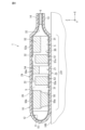
- FIG. 1 is a schematic plan view showing a first embodiment of a stretchable device.
- 2 is a sectional view taken along line II-II in FIG. 1.
- FIG. 2 is a sectional view taken along line II-II in FIG. 1.
- FIG. 2 is a sectional view taken along line II-II in FIG. 1.
- FIG. 3 is an enlarged view including the vicinity of the first electronic component in FIG. 2.
- FIG. 3 is a cross-sectional view of a second embodiment of a stretchable device.
- FIG. 7 is a cross-sectional view of a third embodiment of a stretchable device.
- FIG. 4 is a cross-sectional view of a fourth embodiment of a stretchable device.
- FIG. 1 is a schematic plan view showing a first embodiment of a stretchable device.
- FIG. 2 is a sectional view taken along line II-II in FIG.
- the stretchable device 1 includes a stretchable substrate 10 that can be stretched and contracted, and a plurality of electronic components 51 to 55 provided on the stretchable substrate 10.
- the stretchable device 1 is, for example, attached to the body surface of a living body and used for sensing biological signals, healing, and treatment.
- the stretchable device 1 is a biological interface circuit module having flexibility and stretchability.
- on the stretchable substrate does not refer to an absolute direction such as vertically upward defined by the direction of gravity, but rather to the outside and inside of the stretchable substrate with the surface of the stretchable substrate as the boundary. It refers to the direction towards the outside. Therefore, “on the stretchable substrate” is a relative direction determined by the orientation of the surface of the stretchable substrate. Furthermore, “above” an element does not only mean a position directly above the element (on), but also a position above the element that is away from it, that is, a position above the element through other objects. Also includes spaced above positions.
- the length direction (longitudinal direction) of the stretchable device 1 is assumed to be the X direction.
- the width direction of the stretchable device 1 is defined as the Y direction.
- the thickness direction of the stretchable device 1 is defined as the Z direction.
- the X direction, Y direction, and Z direction are mutually orthogonal directions, and when arranged in the order of X, Y, and Z, form a right-handed system.
- the forward Z direction is also referred to as the upper side of the Z direction
- the reverse Z direction is also referred to as the lower side of the Z direction.
- the stretchable substrate 10 has a first main surface 11 and a second main surface 12.
- the first main surface 11 includes a first region Z1 and a second region Z2.
- the first region Z1 and the second region Z2 are regions where electronic components can be mounted, for example, regions where stretchable wiring connected to the electronic components is provided.
- the stretchable substrate 10 is folded back so that the first main surface 11 is on the inside.
- electronic components may be placed on the first main surface 11.
- the stretchable substrate 10 is folded back so that the first region Z1 and the second region Z2 of the first main surface 11 face each other.
- the electronic component may be placed in at least one of the first region Z1 and the second region Z2.
- the stretchable substrate 10 is folded back so that the first main surface 11 is on the inside, and the electronic components 51 to 55 can be placed on the first main surface 11. Therefore, the plurality of electronic components 51 to 55 are arranged inside the folded stretchable substrate 10. Therefore, the possibility of moisture intruding into the inside of the stretchable substrate 10 can be reduced, and the plurality of electronic components 51 to 55 can be protected from moisture.
- the number of electronic components may be one, and in this case, one electronic component is disposed in at least one of the first region Z1 and the second region Z2, thereby protecting the electronic component from moisture. Can be done.
- the first main surface 11 of the stretchable substrate 10 has a first region Z1 and a second region Z2.
- the first region Z1 is located on the lower side in the Z direction
- the second region Z2 is located on the upper side in the Z direction.
- the first region Z1 and the second region Z2 are each a flat surface and are arranged parallel to each other.
- a flat surface includes not only a completely flat surface but also a substantially flat surface.
- parallel includes not only completely parallel but also substantially parallel.
- at least one of the first region Z1 and the second region Z2 may be bent to some extent. The same applies hereafter.
- the second main surface 12 of the stretchable substrate 10 has a third region Z3 and a fourth region Z4.
- the third region Z3 is located on the opposite side to the first region Z1, and the fourth region Z4 is located on the opposite side to the second region Z2.
- the third region Z3 is located on the lower side in the Z direction, and the fourth region Z4 is located on the upper side in the Z direction.
- the third region Z3 and the fourth region Z4 are each flat surfaces and are arranged parallel to each other.
- the stretchable substrate 10 has a bent portion 15.
- the bent portion 15 extends along the Y direction and is curved to protrude in the reverse X direction.
- a curved apex portion 15a of the bent portion 15 extends in the Y direction.
- the vertex portion 15a is located at the center of the bent portion 15 in the Z direction.
- the stretchable substrate 10 has a first edge portion 13 located on the first region Z1 side and a second edge portion 14 located on the second region Z2 side.
- the first edge portion 13 is a portion located closer to the first region Z1 (third region Z3) than the apex portion 15a of the edge portions around the entire circumference of the stretchable substrate 10.
- the second edge portion 14 is a portion of the peripheral edge portion of the stretchable substrate 10 located closer to the second region Z2 (fourth region Z4) than the apex portion 15a.
- the first edge portion 13 has an end portion 13a facing the apex portion 15a in the X direction, and a side portion 13b located between the apex portion 15a and the end portion 13a.
- the second edge portion 14 has an end portion 14a facing the apex portion 15a in the X direction, and a side portion 14b located between the apex portion 15a and the end portion 14a.
- the end 13a of the first end edge 13 and the end 14a of the second end edge 14 are opposite to each other in the Z direction, and the side 13b of the first end 13 and the side 14b of the second end 14 are opposite to each other in the Z direction. are opposed in the Z direction.
- the electronic components 51 to 55 are surrounded by the first edge portion 13 when viewed from above. Therefore, it is possible to suppress moisture from entering the electronic components 51 to 55 from all sides.
- the connecting member 6 is, for example, an anisotropic conductive adhesive, and has conductivity in the thickness direction and insulation in the planar direction.
- the connecting member 6 includes a thermosetting epoxy resin and conductive particles contained in the resin.
- the first edge portion 13 and at least a portion of the second edge portion 14 are connected to each other via the connecting member 6.
- the possibility of water intrusion can be further reduced.
- the side portion 13b of the first edge portion 13 and the side portion 14b of the second edge portion 14 may be connected via the connecting member 6.
- the stretchable device 1 further includes an elastic member 5 that contacts the first region Z1 and the second region Z2.
- the elastic member 5 is a member having flexibility and elasticity, and is made of, for example, a sponge material such as polyurethane foam or polyester. According to the above configuration, the elastic member 5 is sandwiched between the first region Z1 and the second region Z2 and supports the first region Z1 and the second region Z2, so that strength against external pressure can be ensured.
- the elastic member 5 when the second region Z2 is arranged above the first region Z1 in the direction of gravity, even if the second region Z2 bends under its own weight, the elastic member 5 does not move between the first region Z1 and the second region Z2. Therefore, the second region Z2 can be prevented from coming into contact with the first region Z1.
- the elastic member 5 covers at least a portion of the plurality of electronic components 51 to 55. Thereby, the elastic member 5 can absorb external impact and protect the plurality of electronic components 51 to 55. Further, the elastic member 5 can suppress the infiltration of moisture and protect the plurality of electronic components 51 to 55 from moisture.
- the stretchable substrate 10 includes a stretchable base material 20 that is stretchable and a stretchable wire 30 that is provided on the stretchable base material 20.
- the first main surface 11 includes the surface of the main surface of the stretchable base material 20 that is exposed from the stretchable wiring 30, and the upper surface of the stretchable wire 30 on the opposite side to the lower surface that contacts the stretchable base material 20. It consists of The same applies to the first region Z1 and the second region Z2. Note that the stretchable substrate 10 does not need to have the stretchable wiring 30.
- the first main surface 11 is constituted by the main surface of the stretchable base material 20.
- the stretchable base material 20 is a sheet-like or film-like base material made of a stretchable resin material, and is folded back in two.
- the resin material is, for example, styrene resin, olefin resin, epoxy resin, urethane resin, acrylic resin, or silicone resin, preferably urethane resin.
- the urethane resin include thermoplastic polyurethane.
- the styrene resin include styrene-butadiene-styrene copolymer resin.
- the stretch rate of the stretchable base material 20 is preferably 50% or more. By setting the stretch ratio as described above, the stretchable device 1 can better follow the living body.
- the Young's modulus of the stretchable base material 20 is preferably 100 MPa or less, more preferably 30 MPa or less. By setting the Young's modulus as described above, the user's discomfort can be suppressed.
- the water absorption rate of the stretchable base material 20 is preferably 1% by weight or less from the viewpoint of more reliably ensuring the reliability of the stretchable device 1.
- the thickness of the stretchable base material 20 is, for example, 0.1 ⁇ m or more and 100 ⁇ m or less.
- the width of the stretchable base material 20 is, for example, 10 mm or more and 100 mm or less.
- the stretchable wiring 30 extends along the main surface of the stretchable base material 20.
- the stretchable wiring 30 may extend not only in one direction on the XY plane, but also while bending in a plurality of directions on the XY plane.
- the stretchable wiring 30 may be embedded in the stretchable base material 20 such that a part of the stretchable wire 30 is exposed from the main surface of the stretchable base material 20.
- the stretchable wiring 30 is made of a stretchable conductive material.
- metal foil such as silver, copper, or nickel may be used as the conductive material, or metal powder such as silver, copper, or nickel and elastomeric resin such as epoxy resin, urethane resin, acrylic resin, or silicone resin may be used.
- the metal powder is preferably silver. Thereby, the stretchable wiring 30 with low resistance can be formed.
- the average particle D50 of the metal powder is preferably 0.01 ⁇ m or more and 10 ⁇ m or less.
- the shape of the metal powder may be spherical, flat, irregularly shaped with protrusions, etc.
- the thickness of the stretchable wiring 30 is preferably 100 ⁇ m or less, more preferably 50 ⁇ m or less, and preferably 1 ⁇ m or more, more preferably 10 ⁇ m or more.
- the width of the stretchable wiring 30 is preferably 0.2 mm or more.
- the stretchable wiring 30 is formed by screen printing, inkjet printing, dispensing, etc. so as to be in direct contact with the main surface of the stretchable base material 20. Note that the stretchable wiring 30 may be arranged on the main surface of the stretchable base material 20 with an insulating protective film (not shown) interposed therebetween.
- the stretchable wiring 30 has a first wiring part 31 provided on the first region Z1 side and a second wiring part 32 provided on the second region Z2 side.
- the first wiring portion 31 is a portion of the stretchable wiring 30 located closer to the first region Z1 than the vertex portion 15a.
- the second wiring portion 32 is a portion of the stretchable wiring 30 located closer to the second region Z2 than the vertex portion 15a.
- the first wiring section 31 and the second wiring section 32 are electrically connected. Specifically, the first wiring section 31 and the second wiring section 32 are connected via the connecting member 6 on the end portions 13a and 14a side. On the other hand, on the bending part 15 side, the first wiring part 31 and the second wiring part 32 are directly connected. Note that the first wiring portion 31 and the second wiring portion 32 may be electrically connected at one of the end portions 13a and 14a side or the bent portion 15 side.
- the connecting member 6 can be used to electrically connect the first wiring part 31 and the second wiring part 32, and to connect the first edge part 13 and the second end. It can also be used for the physical connection of the edge 14.
- the plurality of electronic components 51 to 55 include a first electronic component 51, a second electronic component 52, a third electronic component 53, a fourth electronic component 54, and a fifth electronic component 55.
- the first electronic component 51 is a temperature sensor that measures the temperature of a living body.
- the second electronic component 52 is a BLE module that includes an antenna and wirelessly communicates signals.
- the third electronic component 53 is an acceleration sensor that measures the acceleration of a living body.
- the fourth electronic component 54 is an LED that measures SpO2 (percutaneous arterial oxygen saturation).
- the fifth electronic component 55 is a battery that serves as a power source for operating the circuit. Note that it may also include other electronic components such as a coil that irradiates electromagnetic waves into the body, an ultrasonic oscillator that irradiates ultrasonic waves into the body, and a light receiving sensor.
- the plurality of electronic components 51 to 55 are arranged in both the first region Z1 and the second region Z2. That is, the first electronic component 51 is arranged in the first region Z1, and the second electronic component 52 is arranged in the second region Z2.
- the first electronic component 51 is arranged in the first region Z1
- the second electronic component 52 is arranged in the second region Z2.
- the portion of the stretchable substrate 10 where the electronic components are installed is compared to the portion of the stretchable substrate 10 where no electronic components are installed. It becomes hard.
- the second main surface of the stretchable board is placed on the human body surface in a state where the stretchable board is unfolded without being folded back as in the past, the user may I feel discomfort due to the hardness. Particularly in areas where electronic components are mounted at a high density, the impact on the user is significant.
- the size of the stretchable substrate is increased in order to lower the mounting density of electronic components, there is a problem in that the dead space on the first main surface of the stretchable substrate increases. Furthermore, if the stretchable substrate is made larger, the locations on the human body to which it can be attached will be limited.
- a plurality of electronic components can also be provided in the second region Z2 on the back side of the fourth region Z4 on the side that does not come into contact with the human body. Even if the mounting density of electronic components on the first main surface 11 is increased and the dead space on the first main surface 11 of the stretchable substrate 10 is reduced, the user's discomfort can be reduced. For example, a small-sized electronic component can be placed on the first region Z1 side, and a large-sized electronic component can be placed on the second region Z2 side.
- the stretchable substrate 10 since the stretchable substrate 10 is used by being bent, the area of the contact surface of the stretchable substrate 10 that comes into contact with the body surface is reduced, reducing discomfort for the user, and it also stretches and contracts according to the location on the human body to which it is attached. The size of the sexual substrate can be adjusted.
- the third electronic component 53 is arranged in the first region Z1
- the fourth electronic component 54 is arranged in the second region Z2. According to the above configuration, even if the mounting density of electronic components is increased and the dead space on the first main surface 11 of the stretchable substrate 10 is reduced, the user's discomfort can be reduced.
- the fifth electronic component 55 is arranged so as to contact both the first region Z1 and the second region Z2.
- the first electronic component 51, the second electronic component 52, the third electronic component 53, the fourth electronic component 54, and the fifth electronic component 55 are each connected to the stretchable wiring 30. Specifically, the first electronic component 51, the third electronic component 53, and the fifth electronic component 55 are each connected to the first wiring section 31. The second electronic component 52, the fourth electronic component 54, and the fifth electronic component 55 are each connected to the second wiring section 32.
- the first electronic component 51 and the third electronic component 53 are body surface close type electronic components.
- a body surface close type electronic component is an electronic component that is preferably placed close to the body surface.
- the temperature sensor (first electronic component 51) and acceleration sensor (third electronic component 53) are preferably mounted close to the body surface in order to measure highly accurate data.
- the second electronic component 52 and the fourth electronic component 54 are body surface-separated electronic components.
- a body surface-separated type electronic component is an electronic component that is preferably placed away from the body surface. Specifically, since the LED (second electronic component 52) has a light emitting part on the top surface of the component, it is necessary to mount the LED (second electronic component 52) on the side opposite to the body surface so that the top surface of the component is on the body surface side. Since the BLE module (fourth electronic component 54) has the property that the human body absorbs radio waves, the communication state can be improved if the BLE module (fourth electronic component 54) is mounted at a position as far away from the human skin as possible.
- the first electronic component 51 and The third electronic component 53 is placed on the side closer to the body surface, and the second electronic component 52 and the fourth electronic component 54 are placed on the side farther from the body surface.
- the first electronic component 51 and the second electronic component 52 do not overlap in the direction perpendicular to the first region Z1.
- the direction perpendicular to the first region Z1 corresponds to the Z direction.
- the first electronic component 51 and the second electronic component 52 do not interfere with each other in the direction perpendicular to the first region Z1. Thereby, the thickness of the stretchable device 1 can be reduced so that the first region Z1 and the second region Z2 are brought closer to each other.
- the first electronic component 51 and the fourth electronic component 54 do not overlap in the direction perpendicular to the first region Z1.
- the second electronic component 52 and the third electronic component 53 do not overlap in the direction perpendicular to the first region Z1.
- the third electronic component 53 and the fourth electronic component 54 do not overlap in the direction perpendicular to the first region Z1.
- the fifth electronic component 55 does not overlap with the first to fourth electronic components 51 to 54 in the direction orthogonal to the first region Z1.
- the electronic components may overlap when viewed from the direction orthogonal to the first region Z1, and in this case, the planar area of the stretchable base material 20 when viewed from the direction orthogonal to the first region Z1 can be further reduced.
- the elastic member 5 between the upper and lower electronic components, interference between the upper and lower electronic components can be suppressed.
- the first electronic component 51 and the second electronic component 52 overlap in the direction parallel to the first region Z1.
- the direction orthogonal to the first region Z1 corresponds to the XY plane direction.
- the first electronic component 51 and the second electronic component 52 can be arranged so as not to interfere with each other in the direction orthogonal to the first region Z1. Thereby, the thickness of the stretchable device 1 can be reduced so that the first region Z1 and the second region Z2 are brought closer to each other.
- the first electronic component 51 and the fourth electronic component 54 overlap in the direction parallel to the first region Z1.
- the second electronic component 52 and the third electronic component 53 overlap in a direction parallel to the first region Z1.
- the third electronic component 53 and the fourth electronic component 54 overlap in a direction parallel to the first region Z1.
- the fifth electronic component 55 overlaps with the first to fourth electronic components 51 to 54 in the direction parallel to the first region Z1. Note that the electronic components do not need to overlap in the direction parallel to the first region Z1.
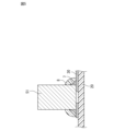
- FIG. 3 is a cross-sectional view taken along line II-II in FIG. 1.
- the sum of the first thickness T1 of the first electronic component 51 and the second thickness T2 of the second electronic component 52 is greater than the longest distance L between the first region Z1 and the second region Z2. It's also big.
- the thickness refers to the size in the direction orthogonal to the first region Z1, and the longest distance refers to the longest size in the direction orthogonal to the first region Z1.
- the first electronic component 51 and the second electronic component 52 can be arranged so as not to interfere with each other in the direction orthogonal to the first region Z1. Thereby, the thickness of the stretchable device 1 can be reduced so that the first region Z1 and the second region Z2 are brought closer to each other.
- the sum of the first thickness T1 of the first electronic component 51 and the fourth thickness T4 of the fourth electronic component 54 is greater than the longest distance L.
- the sum of the second thickness T2 of the second electronic component 52 and the third thickness T3 of the third electronic component 53 is greater than the longest distance L.
- the sum of the third thickness T3 of the third electronic component 53 and the fourth thickness T4 of the fourth electronic component 54 is greater than the longest distance L. Note that the total thickness of a pair of upper and lower electronic components may be smaller than the longest distance.
- FIG. 4 is a cross-sectional view taken along line II-II in FIG. 1.
- the third region Z3 of the second main surface 12 of the stretchable substrate 10 has a body surface region Z31 that can be brought into contact with the body surface 100.
- body surface 100 represents the skin of a human body.
- the total area of the installation surfaces of the plurality of electronic components 51 to 55 installed in the first region Z1 and the second region Z2 is larger than the area of the body surface region Z31.
- the installation surface is not limited to a surface that directly contacts the stretchable substrate 10, but is a surface that faces the stretchable substrate 10 when installed on the stretchable substrate 10.
- the installation surface 51a of the first electronic component 51 is a surface facing the first region Z1.
- the installation surface 52a of the second electronic component 52 is a surface facing the second region Z2.
- the installation surface 53a of the third electronic component 53 is a surface facing the first region Z1.
- the installation surface 54a of the fourth electronic component 54 is a surface facing the second region Z2.
- the first installation surface 55a of the fifth electronic component 55 is a surface facing the first region Z1
- the second installation surface 55b of the fifth electronic component 55 is a surface facing the second region Z2.
- the total area of each of the installation surfaces 51a, 52a, 53a, 54a, 55a, and 55b is larger than the area of the body surface region Z31.
- FIG. 5 is an enlarged view including the vicinity of the first electronic component 51 in FIG. 2.
- the first electronic component 51 is connected to the stretchable wiring 30 via the joint 7 .
- the joint portion 7 is made of, for example, a conductive member such as solder.
- the joint portion 7 is covered with a covering portion 8 .
- the covering portion 8 is made of a resin such as a thermosetting epoxy resin, for example. Thereby, the joint portion 7 can be protected from mechanical stress due to expansion and contraction of the stretchable substrate 10 (stretchable base material 20 and stretchable wiring 30).
- the stretchable substrate 10 is developed into a sheet shape, and a plurality of electronic components 51 to 55 are installed in each of the first region Z1 and the second region Z2 of the first main surface 11 of the stretchable substrate 10. Furthermore, the elastic member 5 is provided in at least one of the first region Z1 and the second region Z2.
- the stretchable substrate 10 is folded in half so that the first main surface 11 is on the inside.
- the stretchable substrate 10 is folded back so that the first region Z1 and the second region Z2 face each other.
- the electronic components 51 and 53 installed in the first region Z1 and the electronic components 52 and 54 installed in the second region Z2 do not interfere with each other in the direction perpendicular to the first region Z1.
- FIG. 6 is a cross-sectional view of a second embodiment of a stretchable device.
- FIG. 6 is a diagram corresponding to the II-II cross section in FIG.
- the second embodiment differs from the first embodiment in that no connecting member is provided. This different configuration will be explained below.
- the other configurations are the same as those in the first embodiment, are given the same reference numerals as in the first embodiment, and the description thereof will be omitted.
- the elastic device 1A of the second embodiment does not include the connecting member 6 of the first embodiment. That is, the first edge part 13 and the second edge part 14 are not connected and are separated from each other. Specifically, the end 13a of the first end 13 and the end 14a of the second end 14 are separated from each other.
- the elastic member 5 may not be further provided.
- the connecting member 6 may be provided without providing the elastic member 5.
- FIG. 7 is a cross-sectional view of a third embodiment of a stretchable device.
- FIG. 7 is a diagram corresponding to the II-II cross section in FIG.
- the third embodiment differs from the first embodiment in the number of electronic components. This different configuration will be explained below.
- the other configurations are the same as those in the first embodiment, are given the same reference numerals as in the first embodiment, and the description thereof will be omitted.
- the stretchable device 1B of the third embodiment there is one electronic component, and it is arranged in at least one of the first region Z1 and the second region Z2. Specifically, the first electronic component 51 is arranged in the first region Z1. Note that the first electronic component 51 may be any of the electronic components shown as examples of the electronic components 51 to 55 in paragraph [0036].
- the first electronic component 51 is placed inside the folded stretchable substrate 10. Therefore, the possibility of moisture intruding into the inside of the stretchable substrate 10 can be reduced, and the first electronic component 51 can be protected from moisture.
- one electronic component may be placed in the second area Z2 instead of the first area Z1, or may be placed in contact with both the first area Z1 and the second area Z2.
- FIG. 8 is a cross-sectional view of a fourth embodiment of a stretchable device.
- FIG. 8 is a diagram corresponding to the II-II cross section in FIG.
- the fourth embodiment differs from the first embodiment in that it is composed of multiple types of base materials. This different configuration will be explained below.
- the other configurations are the same as those in the first embodiment, are given the same reference numerals as in the first embodiment, and the description thereof will be omitted.
- the stretchable base material 20 in the first embodiment has a configuration in which it is folded back in two as a whole.
- the stretchable base material 20 having the folded structure has a single shape or one type of continuous shape.
- a plurality of types of base materials take a continuous form, and as a whole, a stretchable composite base material with a folded structure can be configured.
- a first elastic base material 21 and a second base material 22 made of different materials are connected so as to be in contact with each other in the longitudinal direction.
- the second base material 22 is located in a relatively upper part of the stretchable composite base material with a folded structure, and most of the first stretchable base material 21 is located at the bottom. It is located on the side and both are continuous.
- the second base material 22 when the second base material 22 does not include a curved portion due to folding, the second base material 22 may be a base material that does not have elasticity. Specific examples include rigid substrates and FPCs. Moreover, it goes without saying that the second base material may have elasticity. When the second base material has stretchability, the second base material may include a curved portion.
- the first stretchable base material 21 and the second base material 22 may be made of the same material as the stretchable base material 20 described in the section of the first embodiment. Something can happen.
- the material of the first elastic base material 21 may be one type of resin material selected from the group consisting of styrene resin, olefin resin, epoxy resin, urethane resin, acrylic resin, and silicone resin, and
- the material of the base material 22 (if it has stretchability) may be a different material from the material used for the first stretchable base material.
- a stretchable stretchable substrate having a first main surface and a second main surface; and an electronic component provided on the stretchable substrate,
- the first main surface includes a first region and a second region,
- the stretchable substrate is folded back so that the first main surface is on the inside and the first region and the second region are opposite to each other,
- the electronic component is a stretchable device arranged in at least one of the first region and the second region.
- the stretchable substrate has a first edge portion located on the first region side and a second edge portion located on the second region side, and at least a portion of the first edge portion and a second edge portion located on the second region side.
- the stretchable substrate has a stretchable stretchable base material and stretchable stretchable wiring provided on the stretchable base material,
- the stretchable wiring has a first wiring part provided on the first region side and a second wiring part provided on the second region side,
- the stretchable device according to any one of ⁇ 1> to ⁇ 3>, wherein the first wiring part and the second wiring part are electrically connected.
- the elastic device according to any one of ⁇ 1> to ⁇ 4>, further comprising an elastic member that contacts the first region and the second region.
- a plurality of electronic components exist, The plurality of electronic components include a first electronic component and a second electronic component, The stretchable device according to any one of ⁇ 1> to ⁇ 5>, wherein the first electronic component is arranged in the first region, and the second electronic component is arranged in the second region.
- the first electronic component is a body surface close type electronic component
- the stretchable device according to ⁇ 6>, wherein the second electronic component is a body surface-separated electronic component.
- ⁇ 8> The stretchable device according to ⁇ 6> or ⁇ 7>, wherein the first electronic component and the second electronic component do not overlap in a direction perpendicular to the first region.
- ⁇ 9> Any one of ⁇ 6> to ⁇ 8>, wherein the sum of the thickness of the first electronic component and the thickness of the second electronic component is greater than the longest distance between the first region and the second region.
- the stretchable device described in . ⁇ 10> The stretchable device according to any one of ⁇ 6> to ⁇ 9>, wherein the first electronic component and the second electronic component overlap in a direction parallel to the first region.
- a plurality of electronic components exist, The plurality of electronic components are arranged in both the first region and the second region, The second main surface has a third region opposite to the first region, and the third region has a body surface region that can be contacted with the body surface, The total area of the installation surfaces of the plurality of electronic components installed in the first region and the second region is larger than the area of the body surface region, and the total area is one of ⁇ 1> to ⁇ 3>. Stretchable device as described.
Landscapes
- Engineering & Computer Science (AREA)
- Microelectronics & Electronic Packaging (AREA)
- Structure Of Printed Boards (AREA)
Priority Applications (2)
| Application Number | Priority Date | Filing Date | Title |
|---|---|---|---|
| JP2024528771A JP7747207B2 (ja) | 2022-06-23 | 2023-06-07 | 伸縮性デバイス |
| US18/983,614 US20250120021A1 (en) | 2022-06-23 | 2024-12-17 | Stretchable device |
Applications Claiming Priority (2)
| Application Number | Priority Date | Filing Date | Title |
|---|---|---|---|
| JP2022-101187 | 2022-06-23 | ||
| JP2022101187 | 2022-06-23 |
Related Child Applications (1)
| Application Number | Title | Priority Date | Filing Date |
|---|---|---|---|
| US18/983,614 Continuation US20250120021A1 (en) | 2022-06-23 | 2024-12-17 | Stretchable device |
Publications (1)
| Publication Number | Publication Date |
|---|---|
| WO2023248804A1 true WO2023248804A1 (ja) | 2023-12-28 |
Family
ID=89379640
Family Applications (1)
| Application Number | Title | Priority Date | Filing Date |
|---|---|---|---|
| PCT/JP2023/021213 Ceased WO2023248804A1 (ja) | 2022-06-23 | 2023-06-07 | 伸縮性デバイス |
Country Status (3)
| Country | Link |
|---|---|
| US (1) | US20250120021A1 (https=) |
| JP (1) | JP7747207B2 (https=) |
| WO (1) | WO2023248804A1 (https=) |
Citations (7)
| Publication number | Priority date | Publication date | Assignee | Title |
|---|---|---|---|---|
| JPS6462754A (en) * | 1987-09-02 | 1989-03-09 | Oki Electric Ind Co Ltd | Manufacture of thin electronic appliance |
| JP2010016339A (ja) * | 2008-06-03 | 2010-01-21 | Nippon Mektron Ltd | 多層フレキシブルプリント回路基板を用いたモジュールおよびその製造方法 |
| JP2010192883A (ja) * | 2009-01-20 | 2010-09-02 | Sumitomo Bakelite Co Ltd | 光電気混載基板および光電気混載基板の製造方法 |
| JP2013191621A (ja) * | 2012-03-12 | 2013-09-26 | Fujifilm Corp | 回路基板モジュールならびにその製造装置および製造方法 |
| US20150098196A1 (en) * | 2012-05-18 | 2015-04-09 | Advanced Bionics Ag | Printed circuit board apparatus and methods of making the same |
| WO2020158031A1 (ja) * | 2019-01-30 | 2020-08-06 | 株式会社村田製作所 | 伸縮性実装基板 |
| JP2021072428A (ja) * | 2019-11-01 | 2021-05-06 | 株式会社サトーセン | 回路基板およびその製造方法 |
Family Cites Families (2)
| Publication number | Priority date | Publication date | Assignee | Title |
|---|---|---|---|---|
| JP2003347503A (ja) | 2002-05-30 | 2003-12-05 | Hitachi Ltd | 半導体装置及びその製造方法並びに半導体実装方法 |
| WO2019058259A1 (en) | 2017-09-19 | 2019-03-28 | Idex Asa | DUAL-SIDED SENSOR MODULE SUITABLE FOR INTEGRATION IN ELECTRONIC DEVICES |
-
2023
- 2023-06-07 WO PCT/JP2023/021213 patent/WO2023248804A1/ja not_active Ceased
- 2023-06-07 JP JP2024528771A patent/JP7747207B2/ja active Active
-
2024
- 2024-12-17 US US18/983,614 patent/US20250120021A1/en active Pending
Patent Citations (7)
| Publication number | Priority date | Publication date | Assignee | Title |
|---|---|---|---|---|
| JPS6462754A (en) * | 1987-09-02 | 1989-03-09 | Oki Electric Ind Co Ltd | Manufacture of thin electronic appliance |
| JP2010016339A (ja) * | 2008-06-03 | 2010-01-21 | Nippon Mektron Ltd | 多層フレキシブルプリント回路基板を用いたモジュールおよびその製造方法 |
| JP2010192883A (ja) * | 2009-01-20 | 2010-09-02 | Sumitomo Bakelite Co Ltd | 光電気混載基板および光電気混載基板の製造方法 |
| JP2013191621A (ja) * | 2012-03-12 | 2013-09-26 | Fujifilm Corp | 回路基板モジュールならびにその製造装置および製造方法 |
| US20150098196A1 (en) * | 2012-05-18 | 2015-04-09 | Advanced Bionics Ag | Printed circuit board apparatus and methods of making the same |
| WO2020158031A1 (ja) * | 2019-01-30 | 2020-08-06 | 株式会社村田製作所 | 伸縮性実装基板 |
| JP2021072428A (ja) * | 2019-11-01 | 2021-05-06 | 株式会社サトーセン | 回路基板およびその製造方法 |
Also Published As
| Publication number | Publication date |
|---|---|
| US20250120021A1 (en) | 2025-04-10 |
| JPWO2023248804A1 (https=) | 2023-12-28 |
| JP7747207B2 (ja) | 2025-10-01 |
Similar Documents
| Publication | Publication Date | Title |
|---|---|---|
| CN110491882B (zh) | 柔性电路板、显示面板及显示装置 | |
| US20240157669A1 (en) | Display module and display apparatus | |
| EP3120381B1 (en) | Flexible electronics apparatus and associated methods | |
| CN105404880B (zh) | 一种具有指纹传感器组件的电子装置 | |
| US11540388B2 (en) | Flexible circuit board component and display device | |
| CN114220349B (zh) | 用于印刷电路板的保护带和包括保护带的显示装置 | |
| US20180206330A1 (en) | Electromagnetic shielding protection film and fpc | |
| JP2016168289A (ja) | バンド及び電子機器 | |
| JP7440842B2 (ja) | 伸縮配線部材 | |
| CN113362724A (zh) | 显示模组及显示装置 | |
| US20120099282A1 (en) | Electronic Device and Flexible Printed Wiring Board | |
| US11877384B2 (en) | Flexible circuit board, manufacturing method thereof and display panel | |
| US9560749B2 (en) | Electronic devices having stress concentrators for printed circuit boards | |
| US12016117B2 (en) | Extensible and contractible mounting board | |
| WO2023248804A1 (ja) | 伸縮性デバイス | |
| CN119318210A (zh) | 伸缩性器件 | |
| TWI755555B (zh) | 印刷電路板以及具有印刷電路板的電子裝置 | |
| JP7718604B2 (ja) | 伸縮性デバイス | |
| CN222030115U (zh) | 伸缩器件 | |
| JP2017022225A (ja) | 基板及び電子機器 | |
| TW200913802A (en) | Flexible print board | |
| CN112867378B (zh) | 电磁屏蔽膜、显示面板及显示装置 | |
| JP7563632B2 (ja) | 伸縮配線基板 | |
| JP7758216B2 (ja) | 伸縮性デバイス | |
| WO2020166633A1 (ja) | 配線基板及び配線基板の製造方法 |
Legal Events
| Date | Code | Title | Description |
|---|---|---|---|
| 121 | Ep: the epo has been informed by wipo that ep was designated in this application |
Ref document number: 23826991 Country of ref document: EP Kind code of ref document: A1 |
|
| WWE | Wipo information: entry into national phase |
Ref document number: 2024528771 Country of ref document: JP |
|
| NENP | Non-entry into the national phase |
Ref country code: DE |
|
| 122 | Ep: pct application non-entry in european phase |
Ref document number: 23826991 Country of ref document: EP Kind code of ref document: A1 |