WO2023243464A1 - 半導体装置、半導体モジュール、および半導体モジュールの取付構造 - Google Patents
半導体装置、半導体モジュール、および半導体モジュールの取付構造 Download PDFInfo
- Publication number
- WO2023243464A1 WO2023243464A1 PCT/JP2023/020834 JP2023020834W WO2023243464A1 WO 2023243464 A1 WO2023243464 A1 WO 2023243464A1 JP 2023020834 W JP2023020834 W JP 2023020834W WO 2023243464 A1 WO2023243464 A1 WO 2023243464A1
- Authority
- WO
- WIPO (PCT)
- Prior art keywords
- semiconductor
- semiconductor module
- thickness direction
- wiring
- semiconductor devices
- Prior art date
- Legal status (The legal status is an assumption and is not a legal conclusion. Google has not performed a legal analysis and makes no representation as to the accuracy of the status listed.)
- Ceased
Links
Images


Classifications
-
- H—ELECTRICITY
- H10—SEMICONDUCTOR DEVICES; ELECTRIC SOLID-STATE DEVICES NOT OTHERWISE PROVIDED FOR
- H10W—GENERIC PACKAGES, INTERCONNECTIONS, CONNECTORS OR OTHER CONSTRUCTIONAL DETAILS OF DEVICES COVERED BY CLASS H10
- H10W40/00—Arrangements for thermal protection or thermal control
- H10W40/60—Securing means for detachable heating or cooling arrangements, e.g. clamps
-
- H—ELECTRICITY
- H10—SEMICONDUCTOR DEVICES; ELECTRIC SOLID-STATE DEVICES NOT OTHERWISE PROVIDED FOR
- H10W—GENERIC PACKAGES, INTERCONNECTIONS, CONNECTORS OR OTHER CONSTRUCTIONAL DETAILS OF DEVICES COVERED BY CLASS H10
- H10W72/00—Interconnections or connectors in packages
- H10W72/071—Connecting or disconnecting
-
- H—ELECTRICITY
- H10—SEMICONDUCTOR DEVICES; ELECTRIC SOLID-STATE DEVICES NOT OTHERWISE PROVIDED FOR
- H10W—GENERIC PACKAGES, INTERCONNECTIONS, CONNECTORS OR OTHER CONSTRUCTIONAL DETAILS OF DEVICES COVERED BY CLASS H10
- H10W90/00—Package configurations
Definitions
- the present disclosure relates to a semiconductor device, a semiconductor module, and a mounting structure for a semiconductor module.
- Patent Document 1 discloses an example of a semiconductor module including a plurality of semiconductor devices.
- the semiconductor module (intelligent power module) described in Patent Document 1 includes a plurality of semiconductor devices (power semiconductor module). Further, the semiconductor module described in Patent Document 1 includes a cooler and a drive circuit section. Each of the plurality of semiconductor devices is joined to a cooler.
- Each of the plurality of semiconductor devices includes a sealed body and a plurality of lead terminals.
- a sealing body seals a semiconductor element (semiconductor device).
- the plurality of lead terminals are bent upward and extend above the sealing body.
- the drive circuit section includes a drive circuit board on which a drive circuit for driving each semiconductor device is mounted, and is provided in common for a plurality of semiconductor devices.
- the drive circuit section is arranged above the plurality of semiconductor devices.
- a plurality of through holes are formed in the drive circuit section.
- a plurality of lead terminals are individually inserted into the plurality of through holes.
- the semiconductor device (power module) disclosed in Patent Document 2 includes a semiconductor element (semiconductor chip), a lead terminal, and a sealed body (package).
- the semiconductor device is bonded (fixed) to a heat sink serving as a support member.
- the semiconductor module described in Patent Document 1 if there are variations in the relative positional relationship of the plurality of semiconductor devices, variations occur in the positions of the plurality of lead terminals among the plurality of semiconductor devices. If there are variations in the positions of the plurality of lead terminals, the positional relationship between the plurality of lead terminals and the plurality of through holes provided in the drive circuit section will not match, and the drive circuit section will be connected to the plurality of semiconductor devices. It is difficult to do so. Further, the semiconductor device described in Patent Document 2 still has room for improvement in terms of fixing to a support member.
- an object of the present disclosure to provide a semiconductor device, a semiconductor module, and a mounting structure for a semiconductor module that are improved over conventional ones.
- an object of the present disclosure is to provide a semiconductor module that can suppress variations in the relative positional relationship of a plurality of semiconductor devices.
- Another object of the present disclosure is to provide a semiconductor device (and semiconductor module) that can be easily fixed to a support member.
- a semiconductor module provided by a first aspect of the present disclosure includes a semiconductor element, a sealing part that covers the semiconductor element, and a part that protrudes from the sealing part in a thickness direction of the sealing part and is electrically connected to the semiconductor element.
- a plurality of semiconductor devices each of which is provided with a signal terminal, and a connecting portion that connects the plurality of semiconductor devices, the plurality of semiconductor devices are adjacent to each other in a first direction orthogonal to the thickness direction.
- the connecting portion includes a first device and a second device, and the connecting portion is a first connection that is located between the first device and the second device in the first direction and connects the first device and the second device.
- a semiconductor module mounting structure provided by a second aspect of the present disclosure includes: a semiconductor module provided by the first aspect; a heat sink to which the semiconductor module is attached and in contact with each of the plurality of semiconductor devices; Equipped with
- a semiconductor device provided by a third aspect of the present disclosure includes a semiconductor element, a sealing resin that covers the semiconductor element, a terminal that is electrically connected to the semiconductor element, and a plate that is not electrically conductive to the semiconductor element.
- the sealing resin has a top surface and a bottom surface facing opposite to each other in the thickness direction of the sealing resin, and a plurality of resin side surfaces each connected to the top surface, and the terminal is connected to the sealing resin.
- the plate protrudes from the stopper resin, and the plate protrudes from any one of the plurality of resin side surfaces.
- a semiconductor module provided by a fourth aspect of the present disclosure includes the semiconductor device provided by the third aspect and a heat sink in contact with the bottom surface, and the plate is fixed to the heat sink.
- the semiconductor module mounting structure it is possible to suppress variations in the relative positional relationship of the plurality of semiconductor devices in the semiconductor module. Furthermore, in the semiconductor module mounting structure, the accuracy of positioning a plurality of semiconductor devices with respect to the heat sink can be improved. Furthermore, the semiconductor device can be easily fixed to a support member. Further, in the semiconductor module, the semiconductor device can be properly fixed to the heat sink as a supporting member.
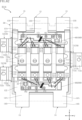
- FIG. 1 is a perspective view showing a semiconductor module according to a first embodiment.
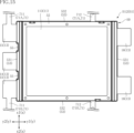
- FIG. 2 is a plan view showing the semiconductor module according to the first embodiment.
- FIG. 3 is a diagram showing the sealing portion with imaginary lines in the plan view of FIG. 2.
- FIG. 4 is a plan view of the main part of FIG. 3.
- FIG. 5 is a bottom view showing the semiconductor module according to the first embodiment.
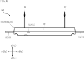
- FIG. 6 is a front view showing the semiconductor module according to the first embodiment.
- FIG. 7 is a rear view of the semiconductor module according to the first embodiment.
- FIG. 8 is a left side view showing the semiconductor module according to the first embodiment.
- FIG. 9 is a right side view showing the semiconductor module according to the first embodiment.
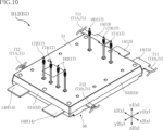
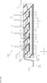
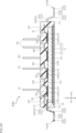
- FIG. 10 is a perspective view showing a semiconductor device (second device) of the semiconductor module according to the first embodiment.
- FIG. 11 is a plan view showing the semiconductor device (second device) of the semiconductor module according to the first embodiment.
- FIG. 12 is a diagram showing the sealing portion with imaginary lines in the plan view of FIG. 11.
- FIG. 13 is a plan view of FIG. 12 in which the sealing portion and the second conductive member are omitted.
- FIG. 14 is a plan view of FIG. 13 with the first conductive member omitted.
- FIG. 15 is a bottom view showing the semiconductor device (second device) of the semiconductor module according to the first embodiment.
- FIG. 16 is a sectional view taken along line XIV-XIV in FIG. 12.
- FIG. 17 is a partially enlarged sectional view of a part of FIG.
- FIG. 16 is near the first element.
- FIG. 18 is a partially enlarged sectional view of a part of FIG. 16 (near the second element).
- FIG. 19 is a cross-sectional view taken along line XIX-XIX in FIG. 12.
- FIG. 20 is a cross-sectional view taken along line XX-XX in FIG. 12.
- FIG. 21 is a sectional view taken along line XXI-XXI in FIG. 12.
- 22 is a sectional view taken along line XXII-XXII in FIG. 12.
- FIG. 23 is a sectional view taken along line XXIII-XXIII in FIG. 12.
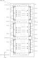
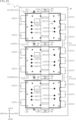
- FIG. 24 is a plan view showing the mounting structure of the semiconductor module according to the first embodiment.
- FIG. 25 is a plan view of FIG.
- FIG. 26 is a front view showing the semiconductor module mounting structure according to the first embodiment.
- FIG. 27 is a left side view showing the mounting structure for the semiconductor module according to the first embodiment.
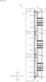
- FIG. 28 is a partially enlarged sectional view of the semiconductor module mounting structure according to the first embodiment.
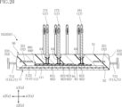
- FIG. 29 is a plan view showing a semiconductor module and a mounting structure for the semiconductor module according to a first modification of the first embodiment.
- FIG. 30 is a left side view showing a semiconductor module and a mounting structure for the semiconductor module according to the first modification of the first embodiment.
- FIG. 31 is a cross-sectional view showing a semiconductor module according to a second modification of the first embodiment, and corresponds to the cross-section of FIG. 23.
- FIG. 32 is a plan view showing a semiconductor module according to the second embodiment.
- FIG. 33 is a plan view of essential parts of a semiconductor module according to the second embodiment.
- FIG. 34 is a sectional view of a main part of a semiconductor module according to a second embodiment.
- FIG. 35 is a plan view of main parts showing a semiconductor module according to a modification of the second embodiment.
- FIG. 36 is a sectional view of a main part of a semiconductor module according to a modification of the second embodiment, and corresponds to the cross section of FIG. 21.
- FIG. 37 is a sectional view of a main part of a semiconductor module according to a modification of the second embodiment, and corresponds to the cross section of FIG. 22.
- FIG. 38 is a plan view showing a semiconductor module according to the third embodiment.
- FIG. 39 is a plan view showing a semiconductor module according to the fourth embodiment.
- FIG. 40 is a plan view showing a semiconductor module according to a first modification of the fourth embodiment.
- FIG. 41 is a plan view showing a semiconductor module according to a second modification of the fourth embodiment.
- FIG. 42 is a plan view showing an example of the configuration when the configuration of the second strip portion of the fourth embodiment is applied to the semiconductor module according to the second embodiment.
- FIG. 43 is a perspective view showing a semiconductor device according to the fifth embodiment.
- FIG. 44 is a plan view showing a semiconductor device according to the fifth embodiment.
- FIG. 45 is a diagram showing the sealing resin with imaginary lines in the plan view of FIG. 44.
- FIG. 46 is a partially enlarged view of FIG. 45.
- FIG. 45 is a diagram showing the sealing resin with imaginary lines in the plan view of FIG. 44.
- FIG. 47 is a diagram in which the second conductive member, the sealing resin, and the plate are omitted from the plan view of FIG. 45, and the first conductive member is shown in imaginary lines.
- FIG. 48 is a right side view showing the semiconductor device according to the fifth embodiment.
- FIG. 49 is a bottom view of the semiconductor device according to the fifth embodiment.
- FIG. 50 is a sectional view taken along line LL in FIG. 45.
- FIG. 51 is a sectional view taken along the LI-LI line in FIG. 45.
- FIG. 52 is a partially enlarged view of the first element shown in FIG. 51 and its surroundings.
- FIG. 53 is a partially enlarged view of the second element shown in FIG. 51 and its surroundings.
- FIG. 54 is a cross-sectional view taken along the line LIV-LIV in FIG.
- FIG. 55 is a cross-sectional view taken along the LV-LV line in FIG. 45.
- FIG. 56 is a plan view of the semiconductor module of the present disclosure, showing a state in which the semiconductor device according to the fifth embodiment is attached to a heat sink.
- FIG. 57 is a front view of the semiconductor module shown in FIG. 56.
- FIG. 58 is a partially enlarged sectional view of the wiring board of the semiconductor module shown in FIG. 56.
- FIG. 59 is a plan view showing a semiconductor device according to the first modification of the fifth embodiment, in which the sealing resin is shown with imaginary lines.
- FIG. 60 is a cross-sectional view of a semiconductor device according to a second modification of the fifth embodiment, and corresponds to the cross-section of FIG. 54.
- FIG. 60 is a cross-sectional view of a semiconductor device according to a second modification of the fifth embodiment, and corresponds to the cross-section of FIG. 54.
- FIG. 61 is a cross-sectional view showing a semiconductor device according to a third modification of the fifth embodiment, and corresponds to the cross-section of FIG. 54.
- FIG. 62 is a plan view showing a semiconductor device according to a fourth modification of the fifth embodiment, in which a sealing resin is shown with imaginary lines.
- FIG. 63 is a cross-sectional view showing a semiconductor device according to a fifth modification of the fifth embodiment, and corresponds to the cross-section of FIG. 54.
- FIG. 64 is a plan view showing the semiconductor device according to the sixth embodiment, in which the sealing resin is shown with imaginary lines.
- FIG. 65 is a cross-sectional view showing the semiconductor device according to the sixth embodiment, and corresponds to the cross-section of FIG. 54.
- FIG. 66 is a cross-sectional view showing the semiconductor device according to the sixth embodiment, and corresponds to the cross-section of FIG. 55.
- FIG. 67 is a cross-sectional view showing the semiconductor device according to the seventh embodiment, and corresponds to the cross-section of FIG. 54.
- FIG. 68 is a cross-sectional view showing the semiconductor device according to the seventh embodiment, and corresponds to the cross-section of FIG. 55.
- FIGS. 1 to 42 Preferred embodiments of the semiconductor module and semiconductor module mounting structure of the present disclosure will be described below with reference to FIGS. 1 to 42.
- the same or similar components will be denoted by the same reference numerals, and redundant explanation will be omitted.
- Terms such as “first”, “second”, “third”, etc. in this disclosure are used merely as labels and are not necessarily intended to attach a permutation to those objects.
- preferred embodiments of semiconductor devices and semiconductor modules according to other aspects of the present disclosure will be described below with reference to FIGS. 43 to 68.
- the symbols used in FIGS. 1 to 42 (first to fourth embodiments) and the symbols used in FIGS. 43 to 68 are independent from each other.
- the same reference numerals may be used for different members (elements, etc.), and different reference numerals may be used for the same (or similar) members (elements, etc.).
- a thing A is formed on a thing B" and "a thing A is formed on a thing B” mean “a thing A is formed on a thing B" unless otherwise specified.
- A is formed directly on something B
- a thing A is formed on something B, with another thing interposed between them.” including.
- "a certain thing A is placed on a certain thing B” and "a certain thing A is placed on a certain thing B” are used as "a certain thing A is placed on a certain thing B” unless otherwise specified.
- ⁇ It is placed directly on something B,'' and ⁇ A thing A is placed on something B, with another thing interposed between them.'' include.
- an object A is located on an object B
- an object A is in contact with an object B, and an object A is located on an object B.
- an object A overlaps an object B when viewed in a certain direction means, unless otherwise specified, “an object A overlaps all of an object B" and "a certain object A overlaps an object B".
- a certain thing A (the material of the thing) includes a certain material C” means "a case where the thing A (the material of the thing A) consists of a certain material C" and "the main component of the thing A (the material of the thing)”. "is a certain material C”.
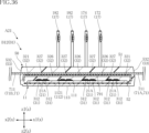
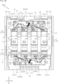
- the semiconductor module A1 is used, for example, as an inverter for driving a three-phase AC motor.
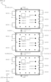
- the semiconductor module A1 includes a plurality of semiconductor devices B1, a connecting portion 71, and an extending portion 72.
- the semiconductor module A1 includes three semiconductor devices B1, but the number of semiconductor devices B1 is not limited to three.
- the semiconductor module A1 constitutes a full bridge circuit, it includes two semiconductor devices B1.
- the thickness direction z corresponds to the thickness direction of the semiconductor module A1.
- plane view refers to when viewed in the thickness direction z.
- the first direction x is orthogonal to the thickness direction z.
- the second direction y is orthogonal to the thickness direction z and the first direction x. Note that one side of the first direction x will be referred to as the x1 side of the first direction x, and the other side of the first direction x will be referred to as the x2 side of the first direction x.
- the plurality of semiconductor devices B1 are arranged at intervals along the first direction x. This interval may be the same or different for each of the two semiconductor devices B1 adjacent in the first direction x.
- Each of the plurality of semiconductor devices B1 includes a plurality of power terminals 13, a plurality of signal terminals 17, a plurality of semiconductor elements 21, and a sealing part 50, as shown in FIGS. 1 to 9.
- the plurality of semiconductor elements 21 are covered with a sealing portion 50.
- the plurality of power terminals 13 protrude from the side surface of the sealing part 50 in the second direction y.
- the plurality of signal terminals 17 protrude from the upper surface (top surface 51 described below) of the sealing portion 50 in the thickness direction z. Note that a detailed configuration example of each semiconductor device B1 will be described later.
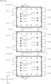
- the plurality of semiconductor devices B1 include a first outer device B21 and a second outer device B22.
- the first outer device B21 is located at the outermost position on the x1 side in the first direction x among the plurality of semiconductor devices B1.
- the first outer device B21 corresponds to the first device B11.
- the second outer device B22 is located at the outermost position on the x2 side in the first direction x among the plurality of semiconductor devices B1.
- the second outer device B22 corresponds to the third device B13.
- the first strip portion 711 is electrically connected to each of the plurality of semiconductor elements 21 of each of the plurality of semiconductor devices B1.
- the first strip portion 711 of the first connecting portion 71A connects one of the plurality of power terminals 13 of the first device B11 (second power terminal 15 described later) and one of the plurality of power terminals 13 of the second device B12. (a second power terminal 15 to be described later).
- the first strip portion 711 of the second connecting portion 71B connects one of the plurality of power terminals 13 of the second device B12 (second power terminal 15 described below) and one of the plurality of power terminals 13 of the third device B13. (a second power terminal 15 to be described later).
- the second strip portion 712 is not electrically connected to any of the plurality of semiconductor elements 21 of each of the plurality of semiconductor devices B1 (non-conductive). As shown in FIG. 4, the second strip portion 712 includes a covering portion 7121, a covering portion 7122, and an exposed portion 7123 in each of the first connecting portion 71A and the second connecting portion 71B.
- the extending portion 72 is not electrically connected to any of the plurality of semiconductor elements 21 of each of the plurality of semiconductor devices B1 (non-conductive). As shown in FIGS. 2 to 4, the extension section 72 has a first extension section 721 and a second extension section 722.
- the first extending portion 721 protrudes from the first outer device B21 (first device B11) toward the x1 side in the first direction x.
- the first extending portion 721 has a band shape whose longitudinal direction is the first direction x.
- the first extending portion 721 includes a covering portion 7211 and an exposed portion 7212.
- the covering portion 7211 is covered by the sealing portion 50 of the first device B11.
- the exposed portion 7212 is connected to the covering portion 7211 and exposed from the sealing portion 50 of the first device B11.
- the second extending portion 722 protrudes from the second outer device B22 (third device B13) toward the x2 side in the first direction x.
- the second extending portion 722 has a band shape whose longitudinal direction is in the first direction x.
- the second extending portion 722 includes a covering portion 7221 and an exposed portion 7222.
- the covering portion 7221 is covered by the sealing portion 50 of the third device B13.
- the exposed portion 7222 is connected to the covering portion 7221 and exposed from the sealing portion 50 of the third device B13.
- the first extending portion 721 has a first through hole 7210.
- the first through hole 7210 is formed in an exposed portion 7212 of the first extending portion 721 .
- the first through hole 7210 penetrates the first extending portion 721 in the thickness direction z.
- the second extending portion 722 has a second through hole 7220.
- the second through hole 7220 is formed in the exposed portion 7222 of the second extending portion 722 .
- the second through hole 7220 penetrates the second extending portion 722 in the thickness direction z.
- either or both of the third through hole 710 of the first connecting portion 71A and the third through hole 710 of the second connecting portion 71B may be opened in a perfect circle in plan view.
- the opening shapes of the first through hole 7210, the second through hole 7220, and each third through hole 710 of the first connecting portion 71A and the second connecting portion 71B in plan view are a perfect circle or a long hole. It may be either.
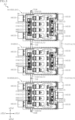
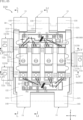
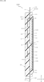
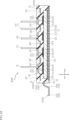
- each semiconductor device B1 (each of the first device B11, second device B12, and third device B13) includes a support substrate 11, a plurality of power terminals 13, a plurality of signal terminals 17, It includes a plurality of semiconductor elements 21, a thermistor 22, a first conductive member 31, a second conductive member 32, a plurality of wires, a sealing part 50, and a pair of control wiring 60.
- the plurality of power terminals 13 include a first power terminal 14, two second power terminals 15, and two third power terminals 16, and the plurality of signal terminals 17 include a first signal terminal 171, a second signal terminal 172, It includes a third signal terminal 173, a fourth signal terminal 174, a fifth signal terminal 181, and a pair of sixth signal terminals 182.
- the plurality of wires include a plurality of first wires 41, a plurality of second wires 42, a plurality of third wires 43, and a plurality of fourth wires 44.
- Each semiconductor device B1 converts the DC power supply voltage applied to the first power terminal 14 and the two second power terminals 15 into AC power using the plurality of semiconductor elements 21.
- the converted AC power is input from the two third power terminals 16 to a power supply target such as a motor.
- the support substrate 11 supports a plurality of semiconductor elements 21 in the thickness direction z, as shown in FIGS. 14, 16 to 19, 21, and 22.
- the support substrate 11 is composed of, for example, a DBC (Direct Bonded Copper) substrate.
- the support substrate 11 includes an insulating layer 111, a first wiring layer 112, and a second wiring layer 113.
- the support substrate 11 is covered with a sealing part 50 except for a part of the second wiring layer 113.
- the insulating layer 111 includes a portion interposed between the first wiring layer 112 and the second wiring layer 113 in the thickness direction z.
- the insulating layer 111 is made of a material with relatively high thermal conductivity.
- the insulating layer 111 is made of ceramics containing aluminum nitride (AlN), for example.
- the insulating layer 111 may be made of an insulating resin sheet instead of ceramics.
- the first wiring layer 112 is located above the insulating layer 111 (on the z1 side) in the thickness direction z.
- the composition of the first wiring layer 112 includes copper (Cu).
- the first wiring layer 112 is surrounded by the periphery of the insulating layer 111 in plan view.
- the first wiring layer 112 includes a first mounting section 1121 and a second mounting section 1122.
- the first mounting section 1121 and the second mounting section 1122 each have a rectangular shape in plan view.
- the first mounting section 1121 and the second mounting section 1122 are separated from each other in the second direction y.
- Each of the plurality of semiconductor elements 21 is bonded to either the first mounting section 1121 or the second mounting section 1122.
- the second wiring layer 113 is located below the insulating layer 111 (on the z2 side) in the thickness direction z. As shown in FIG. 15, the second wiring layer 113 is exposed from the sealing part 50. A heat sink 80, which will be described later, is bonded to the second wiring layer 113.
- the composition of the second wiring layer 113 includes copper.
- the second wiring layer 113 has a rectangular shape in plan view.
- the second wiring layer 113 is surrounded by the periphery of the insulating layer 111 in plan view.
- Each of the plurality of semiconductor elements 21 is mounted on either the first mounting section 1121 or the second mounting section 1122, as shown in FIG. 14 and FIGS. 16 to 19.
- Each semiconductor element 21 is, for example, a MOSFET (Metal-Oxide-Semiconductor Field-Effect Transistor).
- each semiconductor element 21 may be a switching element such as an IGBT (Insulated Gate Bipolar Transistor) or a diode.
- the semiconductor element 21 is an n-channel type MOSFET with a vertical structure.
- Semiconductor element 21 includes a compound semiconductor substrate.
- the composition of the compound semiconductor substrate includes silicon carbide (SiC) or silicon (Si).
- the plurality of semiconductor elements 21 include a plurality of first elements 21A and a plurality of second elements 21B.
- the structure of each of the plurality of second elements 21B is the same as the structure of each of the plurality of first elements 21A.
- the plurality of first elements 21A are mounted on the first mounting section 1121.
- the plurality of first elements 21A are arranged along the first direction x.
- the plurality of second elements 21B are mounted on the second mounting section 1122.
- the plurality of second elements 21B are arranged along the first direction x.
- the plurality of semiconductor elements 21 have a first electrode 211, a second electrode 212, a third electrode 213, and two fourth electrodes 214.
- the first electrode 211 faces either the first mounting section 1121 or the second mounting section 1122.
- a current corresponding to the power before being converted by the semiconductor element 21 flows through the first electrode 211 . That is, the first electrode 211 corresponds to the drain electrode of the semiconductor element 21.
- the second electrode 212 is located on the opposite side from the first electrode 211 in the thickness direction z. A current corresponding to the power converted by the semiconductor element 21 flows through the second electrode 212 . That is, the second electrode 212 corresponds to the source electrode of the semiconductor element 21.
- the third electrode 213 is located on the same side as the second electrode 212 in the thickness direction z.
- a gate voltage for driving the semiconductor element 21 is applied to the third electrode 213 . That is, the third electrode 213 corresponds to the gate electrode of the semiconductor element 21.
- the area of the third electrode 213 is smaller than the area of the second electrode 212 in plan view.
- the two fourth electrodes 214 are located on the same side as the second electrode 212 in the thickness direction z, and adjacent to the third electrode 213 in the first direction x. Located in In the illustrated example, the two fourth electrodes 214 are arranged on both sides of the third electrode 213 with the third electrode 213 in between in the first direction x. The potential of each fourth electrode 214 is equal to the potential of the second electrode 212. Unlike the illustrated example, each semiconductor element 21 may include only one of the two fourth electrodes 214 or may not include either of the two fourth electrodes 214.
- the conductive bonding layer 23 is interposed between either the first mounting portion 1121 or the second mounting portion 1122 and the first electrode 211 of any one of the plurality of semiconductor elements 21. ing.
- the conductive bonding layer 23 is, for example, solder.
- the conductive bonding layer 23 may include a sintered body of metal particles.
- the first electrodes 211 of the plurality of first elements 21A are electrically bonded to the first mounting portion 1121 via the electrically conductive bonding layer 23. Thereby, the first electrodes 211 of the plurality of first elements 21A are electrically connected to the first mounting portion 1121.
- the first electrodes 211 of the plurality of second elements 21B are electrically bonded to the second mounting portion 1122 via the electrically conductive bonding layer 23. Thereby, the first electrodes 211 of the plurality of second elements 21B are electrically connected to the second mounting portion 1122.
- the plurality of power terminals 13 are electrically connected to the plurality of semiconductor elements 21, respectively. A current corresponding to the power before being converted by the plurality of semiconductor elements 21 or a current corresponding to the power after being converted by the plurality of semiconductor elements 21 flows through the plurality of power terminals 13 .
- the plurality of power terminals 13 include a first power terminal 14 , two second power terminals 15 , and two third power terminals 16 .
- the first power terminal 14 is joined to the first mounting portion 1121, as shown in FIGS. 13 and 19. This joining is not limited in any way, and may be performed using a conductive joining material (for example, solder), which is not shown, or by laser welding, or by caulking.
- the first power terminal 14 is electrically connected to the first electrodes 211 of the plurality of first elements 21A via the first mounting portion 1121.
- the first power terminal 14 is a P terminal (positive electrode) to which a DC power supply voltage to be subjected to power conversion is applied. As shown in FIG. 13, the first power terminal 14 is located on the opposite side of the second mounting portion 1122 with the first mounting portion 1121 interposed therebetween in the second direction y.
- the first power terminal 14 extends from the first mounting portion 1121 to one side (y1 side) in the second direction y, and projects from the sealing portion 50 to one side (y1 side) in the second direction y. As shown in FIG. 12, the first power terminal 14 includes a portion covered by the sealing portion 50 and a portion exposed from the sealing portion 50. A portion of the first power terminal 14 covered by the sealing portion 50 is joined to the first mounting portion 1121 . Further, the portion of the first power terminal 14 exposed from the sealing portion 50 is used as the above-mentioned P terminal of each semiconductor device B1.
- a second conductive member 32 is connected to the two second power terminals 15.
- the two second power terminals 15 are electrically connected to the second electrodes 212 of the plurality of second elements 21B via the second conductive member 32.
- the two second power terminals 15 are N terminals (negative electrodes) to which a DC power supply voltage to be subjected to power conversion is applied.
- the two second power terminals 15 are separated from each other in the first direction x.
- the first power terminal 14 is located between the two second power terminals 15 . As shown in FIG. 13, the two second power terminals 15 are each located on the same side as the first power terminal 14 with respect to the first mounting portion 1121 and the second mounting portion 1122 in the second direction y.
- the two second power terminals 15 are separated from the first mounting section 1121 and the second mounting section 1122, respectively.
- the two second power terminals 15 each extend in the second direction y, and protrude from the sealing portion 50 to one side (y1 side) in the second direction y.
- each of the two second power terminals 15 includes a portion covered by the sealing portion 50 and a portion exposed from the sealing portion 50.
- a second conductive member 32 is joined to a portion of each second power terminal 15 covered by the sealing portion 50 . Further, in each second power terminal 15, the portion exposed from the sealing portion 50 is used as the aforementioned N terminal of each semiconductor device B1.
- the first strip portion 711 of the first connection portion 71A described above connects the second power terminal 15 on the x2 side of the two second power terminals 15 of the first device B11 and the two second power terminals of the second device B12. It is connected to the second power terminal 15 on the x1 side among the terminals 15 and is formed integrally therewith.
- the first strip portion 711 of the second connection portion 71B described above connects the second power terminal 15 on the x2 side of the two second power terminals 15 of the second device B12 and the two second power terminals of the third device B13. It is connected to the second power terminal 15 on the x1 side among the terminals 15.
- the two third power terminals 16 are each joined to the second mounting portion 1122, as shown in FIGS. 13 and 16. This joining is not limited in any way, and may be performed using a conductive joining material (for example, solder), which is not shown, or by laser welding, or by caulking.
- the two third power terminals 16 are electrically connected to the first electrodes 211 of the plurality of second elements 21B via the second mounting portions 1122, respectively. Further, the two third power terminals 16 are electrically connected to the second electrodes 212 of the plurality of first elements 21A via the second mounting portion 1122 and the first conductive member 31, respectively.
- AC power converted by the plurality of semiconductor elements 21 (the plurality of first elements 21A and the plurality of second elements 21B) is output from the two third power terminals 16.
- each of the two third power terminals 16 is an output terminal for the AC power.
- the two third power terminals 16 are separated from each other in the first direction x.
- the two third power terminals 16 are each located on the opposite side of the first mounting section 1121 with the second mounting section 1122 interposed therebetween in the second direction y.
- the two third power terminals 16 each extend from the second mounting portion 1122 to the other side (y2 side) in the second direction y, and protrude from the sealing portion 50 to the other side (y2 side) in the second direction y.
- each of the two third power terminals 16 includes a portion covered by the sealing portion 50 and a portion exposed from the sealing portion 50. In each third power terminal 16 , a portion covered by the sealing portion 50 is joined to the second mounting portion 1122 . Further, in each third power terminal 16, the portion exposed from the sealing portion 50 is used as the above-mentioned output terminal of each semiconductor device B1.
- the pair of control wires 60 constitute part of a conductive path between the plurality of signal terminals 17 and the plurality of semiconductor elements 21.
- the pair of control wirings 60 includes a first wiring 601 and a second wiring 602.
- the first wiring 601 is located between the plurality of first elements 21A, the first power terminal 14, and the two second power terminals 15 in the second direction y.
- the first wiring 601 is joined to the first mounting portion 1121, as shown in FIG.
- the second wiring 602 is located between the plurality of second elements 21B and the two third power terminals 16 in the second direction y.
- the second wiring 602 is joined to the second mounting portion 1122, as shown in FIG.
- the pair of control wirings 60 includes an insulating layer 61 , a plurality of wiring layers 62 , a metal layer 63 and a plurality of sleeves 64 .
- the pair of control wires 60 are covered with the sealing portion 50 except for a portion of each of the plurality of sleeves 64 .
- the insulating layer 61, multiple wiring layers 62, metal layers 63, and multiple sleeves 64 described below are common to the pair of control wiring 60 (first wiring 601 and second wiring 602) unless otherwise specified. .
- the plurality of wiring layers 62 are located above the insulating layer 61 in the thickness direction z (on the z1 side).
- the composition of the plurality of wiring layers 62 includes copper.
- the plurality of wiring layers 62 include a first wiring layer 621, a second wiring layer 622, a third wiring layer 623, a fourth wiring layer 624, and a fifth wiring layer 625.
- the metal layer 63 is located on the opposite side from the plurality of wiring layers 62 with the insulating layer 61 in between in the thickness direction z.
- the composition of metal layer 63 includes copper.
- the metal layer 63 of the first wiring 601 is bonded to the first mounting portion 1121 by an adhesive layer (not shown).
- the metal layer 63 of the second wiring 602 is bonded to the second mounting portion 1122 by an adhesive layer (not shown).
- These adhesive layers are made of materials that may or may not be electrically conductive. For example, these adhesive layers are solder.
- each of the plurality of sleeves 64 is bonded to one of the plurality of wiring layers 62 by a conductive bonding layer (for example, solder) not shown.
- the plurality of sleeves 64 are made of a conductive material such as metal.
- Each of the plurality of sleeves 64 has a cylindrical shape extending along the thickness direction z.
- One end of the plurality of sleeves 64 (the edge on the z2 side in the thickness direction z) is electrically conductively bonded to one of the plurality of wiring layers 62.
- the other ends of the plurality of sleeves 64 are exposed from the sealing part 50.
- the thermistor 22 straddles the third wiring layer 623 of the second wiring 602 and the fifth wiring layer 625 of the second wiring 602 and is electrically bonded to them.
- the thermistor 22 is, for example, an NTC (Negative Temperature Coefficient) thermistor.
- the NTC thermistor has a characteristic that its resistance gradually decreases as the temperature rises.
- the thermistor 22 is used as a temperature detection sensor of the semiconductor device B1.
- each of the plurality of signal terminals 17 is made of a metal pin extending in the thickness direction z.
- the plurality of signal terminals 17 protrude from a top surface 51 of the sealing portion 50, which will be described later.
- the plurality of signal terminals 17 are individually press-fitted into the plurality of sleeves 64 of the pair of control wirings 60. Thereby, each of the plurality of signal terminals 17 is supported by one of the plurality of sleeves 64 and is electrically connected to any one of the plurality of wiring layers 62.
- the plurality of signal terminals 17 include a first signal terminal 171 , a second signal terminal 172 , a third signal terminal 173 , a fourth signal terminal 174 , a fifth signal terminal 181 , and a pair of sixth signal terminals 182 .
- the first signal terminal 171 , the second signal terminal 172 , the third signal terminal 173 , the fourth signal terminal 174 , and the fifth signal terminal 181 are electrically connected to any one of the plurality of semiconductor elements 21 .
- the pair of sixth signal terminals 182 are not electrically connected to any of the plurality of semiconductor elements 21 (non-conductive).
- the first signal terminal 171 is press-fitted into the sleeve 64, which is joined to the first wiring layer 621 of the first wiring 601, among the plurality of sleeves 64. Thereby, the first signal terminal 171 is supported by the sleeve 64 and electrically connected to the first wiring layer 621 of the first wiring 601. Further, the first signal terminal 171 is electrically connected to the third electrode 213 of the plurality of first elements 21A. A gate voltage for driving the plurality of first elements 21A is applied to the first signal terminal 171.
- the second signal terminal 172 is press-fitted into the sleeve 64, which is joined to the first wiring layer 621 of the second wiring 602, among the plurality of sleeves 64. Thereby, the second signal terminal 172 is supported by the sleeve 64 and is electrically connected to the first wiring layer 621 of the second wiring 602. Further, the second signal terminal 172 is electrically connected to the third electrode 213 of the plurality of second elements 21B. A gate voltage for driving the plurality of second elements 21B is applied to the second signal terminal 172.
- the third signal terminal 173 is located next to the first signal terminal 171 in the first direction x, as shown in FIGS. 14 and 20. As shown in FIG. 20, the third signal terminal 173 is press-fitted into one of the plurality of sleeves 64, which is joined to the second wiring layer 622 of the first wiring 601. Thereby, the third signal terminal 173 is supported by the sleeve 64 and is electrically connected to the second wiring layer 622 of the first wiring 601. Further, the third signal terminal 173 is electrically connected to the fourth electrode 214 of the plurality of first elements 21A. A voltage corresponding to the maximum current flowing through the fourth electrode 214 of each of the plurality of first elements 21A is applied to the third signal terminal 173.
- the fourth signal terminal 174 is located next to the second signal terminal 172 in the first direction x, as shown in FIGS. 14 and 23. As shown in FIG. 23, the fourth signal terminal 174 is press-fitted into one of the plurality of sleeves 64, which is joined to the second wiring layer 622 of the second wiring 602. Thereby, the fourth signal terminal 174 is supported by the sleeve 64 and electrically connected to the second wiring layer 622 of the second wiring 602. Further, the fourth signal terminal 174 is electrically connected to the fourth electrodes 214 of the plurality of second elements 21B. A voltage corresponding to the maximum current flowing through the fourth electrode 214 of each of the plurality of second elements 21B is applied to the fourth signal terminal 174.
- the fifth signal terminal 181 is located on the opposite side of the first signal terminal 171 with the third signal terminal 173 in between in the first direction x.
- the fifth signal terminal 181 is press-fitted into the sleeve 64 joined to the fifth wiring layer 625 of the first wiring 601, as shown in FIG. Thereby, the fifth signal terminal 181 is supported by the sleeve 64 and electrically connected to the fifth wiring layer 625 of the first wiring 601. Further, the fifth signal terminal 181 is electrically connected to the first mounting portion 1121.
- a voltage corresponding to the DC power input to the first power terminal 14 is applied to the fifth signal terminal 181 .
- the pair of sixth signal terminals 182 are located on the opposite side of the second signal terminal 172 with the fourth signal terminal 174 in between in the first direction x.
- the pair of sixth signal terminals 182 are adjacent to each other in the first direction x.
- the pair of sixth signal terminals 182 are individually press-fitted into a pair of sleeves 64 joined to the third wiring layer 623 of the second wiring 602 and the fifth wiring layer 625 of the second wiring 602, as shown in FIG. ing.
- the pair of sixth signal terminals 182 are individually supported by the pair of sleeves 64 and individually electrically connected to the third wiring layer 623 of the second wiring 602 and the fifth wiring layer 625 of the second wiring 602. are doing.
- the pair of sixth signal terminals 182 are electrically connected to the thermistor 22 .
- the plurality of first wires 41, the plurality of second wires 42, the plurality of third wires 43, and the fourth wires 44 each electrically connect mutually separated parts.
- the plurality of first wires 41, the plurality of second wires 42, the plurality of third wires 43, and the fourth wires 44 are each bonding wires. Note that in FIGS. 3, 4, 12, 16 to 20, and 23, the plurality of first wires 41, the plurality of second wires 42, the plurality of third wires 43, and the fourth wire 44 are omitted. .
- the plurality of first wires 41 are electrically connected to the third electrodes 213 of the plurality of first elements 21A and the fourth wiring layer 624 of the first wiring 601.
- the plurality of third wires 43 are electrically connected to the fourth wiring layer 624 of the first wiring 601 and the first wiring layer 621 of the first wiring 601.
- the first signal terminal 171 is electrically connected to the third electrode 213 of the plurality of first elements 21A.
- the compositions of the plurality of first wires 41 and the plurality of third wires 43 include gold (Au).
- the compositions of the plurality of first wires 41 and the plurality of third wires 43 may include copper or aluminum.
- the plurality of second wires 42 are conductively bonded to either one of the two fourth electrodes 214 of the plurality of first elements 21A and the second wiring layer 622 of the first wiring 601.
- the third signal terminal 173 is electrically connected to either of the two fourth electrodes 214 of the plurality of first elements 21A.
- the plurality of second wires 42 are conductively bonded to either one of the two fourth electrodes 214 of the plurality of second elements 21B and the second wiring layer 622 of the second wiring 602. .
- the fourth signal terminal 174 is electrically connected to either of the two fourth electrodes 214 of the plurality of second elements 21B.
- the composition of the plurality of second wires 42 includes gold.
- composition of the plurality of second wires 42 may include copper or aluminum. Note that when each semiconductor element 21 (each of the plurality of first elements 21A and the plurality of second elements 21B) does not include any of the two fourth electrodes 214, the plurality of second wires 42 One each is bonded to the second electrode 212 of the element 21.
- the fourth wire 44 is conductively bonded to the fifth wiring layer 625 of the first wiring 601 and the first mounting portion 1121.
- the fifth signal terminal 181 is electrically connected to the first electrodes 211 of the plurality of first elements 21A via the first mounting portion 1121.
- the composition of the fourth wire 44 includes gold.
- the composition of the fourth wire 44 may include copper or aluminum.
- the first conductive member 31 is electrically connected to the second electrodes 212 of the plurality of first elements 21A and the second mounting portion 1122, as shown in FIGS. 13 and 16. Thereby, the second electrodes 212 of the plurality of first elements 21A are electrically connected to the second mounting portion 1122.
- the composition of the first conductive member 31 includes copper.
- the first conductive member 31 is a metal clip. As shown in FIGS. 13 and 16, the first conductive member 31 includes a main body 311, a plurality of first joints 312, and a plurality of second joints 313.
- the main body part 311 constitutes the main part of the first conductive member 31. As shown in FIG. 13, the main body portion 311 extends in the first direction x. As shown in FIGS. 13 and 16, the main body portion 311 straddles between the first mounting portion 1121 and the second mounting portion 1122. As shown in FIG. 13, a plurality of through holes 310 are formed in the main body portion 311. Each of the plurality of through holes 310 passes through the main body portion 311 in the thickness direction z. The plurality of through holes 310 overlap between the first mounting section 1121 and the second mounting section 1122 in plan view. Thereby, when forming the sealing part 50, the sealing part 50 can easily flow downward in the thickness direction z of the main body part 311 (z2 side in the thickness direction z).
- each first joint portion 312 extends from the main body portion 311 toward the y1 side in the second direction y.
- the plurality of first joint parts 312 are divided into two from the main body part 311, but they do not need to be divided into two.
- the base end of each first joint portion 312 (the end connected to the main body portion 311) is bent downward in the thickness direction z (to the z2 side in the thickness direction z). Therefore, the tip of each first joint 312 (the end opposite to the side connected to the main body 311) is located below the main body 311 in the thickness direction z (on the z2 side in the thickness direction z). ) located in
- each second joint portion 313 extends from the main body portion 311 toward the y2 side in the second direction y.
- the base end of each second joint portion 313 (the end connected to the main body portion 311) is bent downward in the thickness direction z (to the z2 side in the thickness direction z). Therefore, the tip of each second joint 313 (the end opposite to the side connected to the main body 311) is located below the main body 311 in the thickness direction z (on the z2 side in the thickness direction z). ) located in
- the semiconductor device B1 further includes a first conductive bonding layer 33, as shown in FIGS.
- the first conductive bonding layer 33 is interposed between the second electrodes 212 of the plurality of first elements 21A and the plurality of first bonding portions 312.
- the first conductive bonding layer 33 conductively bonds the second electrodes 212 of the plurality of first elements 21A and the plurality of first bonding portions 312.
- the first conductive bonding layer 33 is, for example, solder.
- the first conductive bonding layer 33 may include a sintered body of metal particles.
- the semiconductor device B1 further includes a second conductive bonding layer 34.
- the second conductive bonding layer 34 is interposed between the second mounting portion 1122 and the second bonding portion 314.
- the second conductive bonding layer 34 conductively bonds the second mounting portion 1122 and the second bonding portion 314 together.
- the second conductive bonding layer 34 is, for example, solder.
- the second conductive bonding layer 34 may include a sintered body of metal particles.
- the second conductive member 32 is electrically connected to the second electrodes 212 of the plurality of second elements 21B and the two second power terminals 15. Thereby, the second electrodes 212 of the plurality of second elements 21B are electrically connected to the two second power terminals 15.
- the composition of the second conductive member 32 includes copper.
- the second conductive member 32 is a metal clip.
- the second conductive member 32 includes a pair of main body parts 321, a plurality of third joint parts 322, a pair of fourth joint parts 324, and a plurality of intermediate parts 326. , a plurality of cross beam portions 327, and a pair of hanging portions 328.
- the pair of main body parts 321 are located apart from each other in the first direction x.
- the pair of main body parts 321 extend in the second direction y.
- the pair of main body parts 321 are arranged parallel to the upper surface of the first mounting part 1121 and the upper surface of the second mounting part 1122.
- the pair of main body parts 321 are located further away from the first mounting part 1121 and the second mounting part 1122 than the main body part 311 of the first conductive member 31 is.
- the plurality of third joints 322 are individually joined to the second electrodes 212 of the plurality of second elements 21B.
- Each of the plurality of third joints 322 faces one of the second electrodes 212 of the plurality of second elements 21B.
- the plurality of third joint portions 322 extend from the plurality of intermediate portions 326 in the first direction x.
- the base end of each third joint portion 322 (the end connected to the intermediate portion 326) is bent downward in the thickness direction z (to the z2 side in the thickness direction z). Therefore, the tip of each third joint portion 322 (the end opposite to the side connected to the intermediate portion 326) is located below the intermediate portion 326 in the thickness direction z (on the z2 side in the thickness direction z). ) located in
- the pair of fourth joints 324 are individually joined to the two second power terminals 15. Each of the pair of fourth joints 324 faces a corresponding one of the two second power terminals 15.
- the plurality of horizontal beams 327 are arranged along the first direction x.
- the plurality of horizontal beam portions 327 include regions that individually overlap the plurality of first joint portions 312 of the first conductive member 31.
- both sides in the first direction x of the cross beam part 327 located at the center in the first direction x among the plurality of cross beam parts 327 are connected to the plurality of intermediate parts 326.
- Both sides of the remaining two cross beam portions 327 in the first direction x among the plurality of cross beam portions 327 are connected to one of the pair of main body portions 321 and one of the plurality of intermediate portions 326.
- the pair of hanging parts 328 are individually connected to the pair of main body parts 321. As shown in FIG. 21, each of the pair of hanging parts 328 extends downward in the thickness direction z (z2 side in the thickness direction z) from a corresponding one of the pair of main body parts 321. Each of the pair of hanging parts 328 is connected to the outer edge of the corresponding one of the pair of main body parts 321 in the first direction x. In the illustrated example, the lower ends (edges on the z2 side in the thickness direction z) of the pair of hanging parts 328 overlap the first mounting part 1121 when viewed along the second direction y.
- the semiconductor device B1 further includes a third conductive bonding layer 35.
- the third conductive bonding layer 35 is interposed between the second electrodes 212 of the plurality of second elements 21B and the plurality of third bonding parts 322.
- the third conductive bonding layer 35 conductively bonds the second electrodes 212 of the plurality of second elements 21B and the plurality of third bonding parts 322.
- the third conductive bonding layer 35 is, for example, solder.
- the third conductive bonding layer 35 may include a sintered body of metal particles.
- the semiconductor device B1 further includes a fourth conductive bonding layer 36.
- the fourth conductive bonding layer 36 is interposed between the two second power terminals 15 and the pair of fourth bonding portions 324 .
- the fourth conductive bonding layer 36 conductively bonds the two second power terminals 15 and the pair of fourth bonding portions 324 .
- the fourth conductive bonding layer 36 is, for example, solder.
- the fourth conductive bonding layer 36 may include a sintered body of metal particles.
- the sealing section 50 includes a plurality of semiconductor elements 21, a first conductive member 31, a second conductive member 32, a plurality of first wires 41, a plurality of second wires 42, and a plurality of Cover the third wire 43. Furthermore, the sealing part 50 covers a portion of each of the support substrate 11 , the plurality of power terminals 13 , and the plurality of signal terminals 17 .
- the sealing portion 50 has electrical insulation properties.
- the sealing portion 50 includes, for example, black epoxy resin.
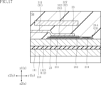
- the sealing portion 50 is formed by, for example, molding. As shown in FIGS. 10 to 12 and 15 to 23, the sealing portion 50 has a top surface 51, a bottom surface 52, a plurality of resin side surfaces 53, and a pair of recesses 55.
- the top surface 51 faces in the same direction as the top surface of the first mounting section 1121 and the top surface of the second mounting section 1122 in the thickness direction z.
- the bottom surface 52 faces opposite to the top surface 51 in the thickness direction z.
- the second wiring layer 113 of the support substrate 11 is exposed from the bottom surface 52.
- the plurality of resin side surfaces 53 are connected to the top surface 51.
- the plurality of resin side surfaces 53 include a pair of first side surfaces 531 and a pair of second side surfaces 532.
- the pair of first side surfaces 531 are located apart from each other in the second direction y.
- the pair of first side surfaces 531 face in the second direction y and extend in the first direction x.
- a pair of first side surfaces 531 are connected to the top surface 51.
- the first power terminal 14 and the two second power terminals 15 respectively protrude from the first side surface 531 on the y1 side in the second direction y of the pair of first side surfaces 531.
- Two third power terminals 16 each protrude from the first side surface 531 on the y2 side in the second direction y of the pair of first side surfaces 531.
- the first extending portion 721 is extended from the second side surface 532 on the x1 side of the pair of second side surfaces 532 of the first device B11. Stick out.
- the second strip portion 712 of the first connecting portion 71A mentioned above protrudes from the second side surface 532 on the x2 side of the pair of second side surfaces 532 of the first device B11, and It protrudes from the second side surface 532 of the second side surface 532 on the x1 side.
- the second strip portion 712 of the second connecting portion 71B mentioned above protrudes from the second side surface 532 on the x2 side of the pair of second side surfaces 532 of the second device B12, and also extends from the second side surface 532 of the second device B13.
- the pair of recesses 55 are recessed from the first side surface 531 of the pair of first side surfaces 531 on the y1 side in the second direction y toward the second direction y.
- the pair of recesses 55 extend from the top surface 51 to the bottom surface 52 in the thickness direction z.
- the pair of recesses 55 are located on both sides of the first power terminal 14 in the second direction y.
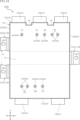
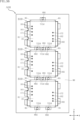
- the mounting structure C1 of the semiconductor module A1 includes the semiconductor module A1, a heat sink 80, a wiring board 81, a mounting member 84, a plurality of positioning pins 86, and a plurality of fastening members 87.
- the heat sink 80 supports the semiconductor module A1 (the plurality of semiconductor devices B1), as shown in FIGS. 26 and 27.
- the heat sink 80 is located on the opposite side of the plurality of semiconductor devices 21 of the plurality of semiconductor devices B1 from the plurality of signal terminals 17 of the plurality of semiconductor devices B1. Therefore, the heat sink 80 faces each second wiring layer 113 of the plurality of semiconductor devices B1.
- the heat sink 80 is made of a material containing aluminum, for example. As shown in FIGS. 24, 25, and 27, the plurality of semiconductor devices B1 are arranged on the heat sink 80 along the first direction x.
- the wiring board 81 is provided in common to the plurality of semiconductor devices B1, as shown in FIGS. 24 and 27. Unlike this configuration, a plurality of wiring boards 81 may be individually provided for a plurality of semiconductor devices B1. As understood from FIGS. 24 and 27, a plurality of signal terminals 17 of a plurality of semiconductor devices B1 are respectively inserted into the wiring board 81 and electrically connected to each signal terminal 17.
- the wiring board 81 is, for example, a gate driver that controls driving of each semiconductor element 21 of the plurality of semiconductor devices B1.
- the wiring board 81 faces the top surface 51 of each sealing section 50 of the plurality of semiconductor devices B1.
- the wiring board 81 is located on the opposite side of the heat sink 80 with respect to the plurality of semiconductor devices B1.
- the wiring board 81 individually overlaps each sealing part 50 of the plurality of semiconductor devices B1 in a plan view.
- FIG. 28 shows a state in which one of the signal terminals 17 of a plurality of semiconductor devices B1 is inserted into a through hole 811A of a substrate 811. Note that all the signal terminals 17 of the plurality of semiconductor devices B1 have the same configuration as shown in FIG. 28.
- each signal terminal 17 has a base 170A and a bulge 170B.
- One side of the base portion 170A in the thickness direction z is press-fitted into one of the plurality of sleeves 64 of the plurality of semiconductor devices B1.
- the bulging portion 170B is provided on one side (z1 side) of the base portion 170A in the thickness direction z.
- the bulging portion 170B bulges in a direction perpendicular to the thickness direction z.
- each signal terminal 17 is press-fitted into one of the plurality of through holes 811A of the wiring board 81.
- the internal wiring 814 placed in any one of the plurality of through holes 811A is pressed against the bulge 170B of the signal terminal 17 inserted through the through hole 811A. Therefore, each signal terminal 17 is electrically connected to the wiring board 81 by being press-fitted into the through hole 811A in the thickness direction z.
- the wiring board 81 is supported by each signal terminal 17 by press-fitting each signal terminal 17 into a corresponding one of the plurality of through holes 811A.
- each of the plurality of positioning pins 86 extends from the upper surface of the heat sink 80 (the surface facing the z1 side in the thickness direction z) to the z1 side in the thickness direction z.
- the plurality of positioning pins 86 may be integrally formed with the heat sink 80 or may be joined to the heat sink 80.
- the plurality of positioning pins 86 are respectively provided in the third through hole 710 of the second strip part 712 of the first connecting part 71A (connecting part 71) and the third through hole 710 of the second belt-like part 712 of the first connecting part 71A (connecting part 71).
- the tip of each positioning pin 86 (the edge on the z1 side in the thickness direction z) is in contact with the wiring board 81.
- the wiring board 81 is supported by the plurality of positioning pins 86.
- a plurality of pillars (not shown) may be arranged on the heat sink 80 or the sealing portion 50 of each semiconductor device B1, and the wiring board 81 may be supported by the plurality of pillars. In this case, the tip of each positioning pin 86 does not need to be in contact with the wiring board 81.
- the attachment member 84 is used to restrain the semiconductor module A1 (the plurality of semiconductor devices B1) to the heat sink 80, as shown in FIGS. 25 to 27.
- the composition of the attachment member 84 includes, for example, metal.
- the mounting member 84 contacts the top surface 51 of each sealing portion 50 of the plurality of semiconductor devices B1.
- the mounting member 84 straddles the top surface 51 of each sealing portion 50 of the plurality of semiconductor devices B1 in the first direction x.
- the mounting member 84 is, for example, a plate spring.
- the mounting member 84 is located between the first signal terminal 171 and the second signal terminal 172 of each semiconductor device B1 in the second direction y.
- the mounting member 84 is located between the heat sink 80 and the wiring board 81 in the thickness direction z.
- Attachment member 84 is partially bent.
- the mounting member 84 contacts the heat sink 80 between the two semiconductor devices B1 adjacent to each other in the first direction x. Furthermore, at least a part of the region of the mounting member 84 that overlaps each sealing portion 50 in plan view contacts the top surface 51 of each sealing portion 50 .
- a plurality of through holes 841 are formed in the mounting member 84 . Each of the plurality of through holes 841 penetrates the attachment member 84 in the thickness direction z. Each of the plurality of through holes 841 is formed in a portion of the mounting member 84 that contacts the heat sink 80 .
- Each of the plurality of fastening members 87 is, for example, a male thread. Each of the plurality of fastening members 87 is inserted into a corresponding one of the plurality of through holes 841, as shown in FIGS. 25 to 27. Each of the plurality of fastening members 87 is fastened to a female threaded hole (not shown) formed in the heat sink 80 . As a result, the plurality of semiconductor devices B1 are restrained by the mounting member 84 and the plurality of fastening members 87.
- the functions and effects of the semiconductor module A1 and the mounting structure C1 for the semiconductor module A1 are as follows.
- the semiconductor module A1 includes a plurality of semiconductor devices B1 and a connecting portion 71.
- the plurality of semiconductor devices B1 includes a first device B11 and a second device B12.
- the connecting portion 71 includes a first connecting portion 71A.
- the first connecting portion 71A is located between the first device B11 and the second device B12 in the first direction x, and connects the first device B11 and the second device B12. According to this configuration, it is possible to suppress variations in the relative positional relationship between the first device B11 and the second device B12 due to the first connecting portion 71A. Therefore, since the semiconductor module A1 can suppress variations in the position of the signal terminals 17 among the plurality of semiconductor devices B1, the wiring board 81 can be appropriately connected to the semiconductor module A1.
- the plurality of semiconductor devices B1 include a first device B11, a second device B12, and a third device B13.
- the connecting portion 71 includes a second connecting portion 71B.
- the second connecting portion 71B is located between the second device B12 and the third device B13 in the first direction x, and connects the second device B12 and the third device B13. According to this configuration, it is possible to suppress variations in the relative positional relationship between the second device B12 and the third device B13 due to the second connection portion 71B.
- the number of semiconductor devices B1 is not limited at all.
- the mounting structure C1 for the semiconductor module A1 includes the semiconductor module A1 and a heat sink 80.
- the semiconductor module A1 can suppress variations in the relative positional relationship of the plurality of semiconductor devices B1, according to the mounting structure C1 of the semiconductor module A1, the semiconductor module A1 can suppress the variation in the relative positional relationship of the plurality of semiconductor devices B1 with respect to the heat sink 80. Positioning accuracy can be improved.
- the semiconductor module A1 includes an extending portion 72.
- the extending portion 72 includes a first extending portion 721 that protrudes from the first outer device B21 toward the x1 side in the first direction x, and a second extending portion 721 that protrudes from the second outer device B22 toward the x2 side in the first direction x.
- the extension portion 722 is included.
- the first extending portion 721 has a first through hole 7210
- the second extending portion 722 has a second through hole 7220.
- the first through hole 7210 and the second through hole 7220 are each inserted into a corresponding one of the plurality of positioning pins 86 formed in the heat sink 80. According to this configuration, it is possible to suppress misalignment of the semiconductor module A1 with respect to the heat sink 80.
- the connecting portion 71 (each of the first connecting portion 71A and the second connecting portion 71B) includes a second strip portion 712.
- the second strip portion 712 of each of the first connecting portion 71A and the second connecting portion 71B has a third through hole 710.
- Each of the third through holes 710 is inserted into a corresponding one of the plurality of positioning pins 86 formed in the heat sink 80 . According to this configuration, misalignment of the semiconductor module A1 with respect to the heat sink 80 can be further suppressed.
- either the first through hole 7210 or the second through hole 7220 has a perfect circular opening when viewed in the thickness direction z.
- the second through hole 7220 opens in a perfect circle.
- the positioning pin 86 is inserted through the perfectly circular opening, thereby suppressing rotation and wobbling of the semiconductor module A1 along the xy plane.
- the other of the first through hole 7210 and the second through hole 7220 opens into a long hole when viewed in the thickness direction z.
- the first through hole 7210 opens into a long hole. This configuration suppresses connection failures of the wiring board 81 to the semiconductor module A1 due to manufacturing errors (manufacturing errors) of each semiconductor device B1.
- the first connection portion 71A includes a first strip portion 711.
- the first strip portion 711 connects the second power terminals 15 of the first device B11 and the second device B12 that are adjacent to each other in the first direction x. According to this configuration, the second power terminal 15 of the first device B11 and the second power terminal 15 of the second device B12 have the same potential.
- the second connecting portion 71B includes a first band-shaped portion 711. The first band-shaped portion 711 connects the second power terminals 15 of the second device B12 and the third device B13 that are adjacent to each other in the first direction x. According to this configuration, the second power terminal 15 of the second device B12 and the second power terminal 15 of the third device B13 have the same potential. For these reasons, the semiconductor module A1 can share the low potential side of the input power supply voltage.
- the connecting portion 71 includes a first connecting portion 71A and a second connecting portion 71B.
- Each of the first connecting portion 71A and the second connecting portion 71B includes a first strip portion 711 and a second strip portion 712.
- the first strip portion 711 is located closer to the y1 side in the second direction y than the second strip portion 712. According to this configuration, it is possible to further suppress variations in the positional relationship of the plurality of semiconductor devices B1.
- FIGS. 29 and 30 show a semiconductor module A11 according to a first modification of the first embodiment and a mounting structure C11 for the semiconductor module A11.
- the semiconductor module A11 differs from the semiconductor module A1 in the following points.
- Each of the second strip portions 712 of the first connecting portion 71A and the second connecting portion 71B of the connecting portion 71 has a portion bent downward in the thickness direction z. Further, the first extending portion 721 and the second extending portion 722 of the extending portion 72 are bent downward in the thickness direction z.
- the plurality of fastening members 87 each have a third through hole 710 in the first connecting portion 71A and a second connecting portion 71B, a first through hole 7210 in the first extending portion 721, and a first through hole 7210 in the first extending portion 721.
- the second extension portion 722 is inserted into a corresponding one of the second through holes 7220 of the second extension portion 722 . Thereby, the semiconductor module A11 is restrained by the heat sink 80.
- the mounting structure C11 for the semiconductor module A11 includes a plurality of supports 88.
- Each of the plurality of pillars 88 is located between the plurality of semiconductor devices B1 and the wiring board 81 in the thickness direction z.
- each of the plurality of pillars 88 is in contact with the top surface 51 of one of the sealing parts 50 of the plurality of semiconductor devices B1, and also in contact with the wiring board 81.
- four pillars 88 are arranged for each semiconductor device B1.
- the four pillars 88 are respectively arranged at the four corners of the region overlapping the wiring board 81 of the sealing portion 50 of the corresponding semiconductor device B1 in plan view.
- the constituent material of the plurality of pillars 88 may include either an insulating resin material or a metal material, but an insulating resin material is preferable in order to suppress unintended short circuits.
- the arrangement and number of the plurality of support columns 88 are not limited to the illustrated example.
- the plurality of support columns 88 may be arranged so as to contact the heat sink 80 instead of being arranged so as to contact the plurality of semiconductor devices B1.
- the semiconductor module A11 can suppress variations in the positional relationship of the plurality of semiconductor devices B1. Further, in the mounting structure C11 for the semiconductor module A11, the semiconductor module A11 is restrained to the heat sink 80 using the connecting portion 71 and the extension portion 72, so the mounting member 84 is not required. However, in order to securely restrain the semiconductor module A11 by the heat sink 80, the mounting structure C11 for the semiconductor module A11 may include a mounting member 84.
- FIG. 31 shows a semiconductor module A12 according to a second modification of the first embodiment.
- the semiconductor module A12 differs from the semiconductor module A1 in the following points. That is, each of the second strip portions 712 and the extension portions 72 (the first extension portion 721 and the second extension portion 722) of the connection portion 71 (the first connection portion 71A and the second connection portion 71B) are insulated. It is.
- each second strip portion 712, first extension portion 721, and second extension portion 722 each contain an insulating material.
- the insulating material is, for example, polycarbonate or glass epoxy resin. Since each of the second strip portions 712, the first extension portions 721, and the second extension portions 722 are insulative, they are joined to the second mounting portion 1122, as shown in FIG. 31.
- the semiconductor module A12 can suppress variations in the positional relationship of the plurality of semiconductor devices B1. Furthermore, in the semiconductor module A12, each of the second strip portions 712, the first extension portions 721, and the second extension portions 722 are bonded to the second mounting portions 1122 of the corresponding semiconductor devices B1, so that these are sealed. It is suppressed from coming off from the stop part 50.
- the semiconductor module A2 is different from the semiconductor module A1 in the configuration of each first strip portion 711 of the first connection portion 71A and the second connection portion 71B (connection portion 71). Note that the semiconductor module A2 is attached to the heat sink 80 similarly to the semiconductor module A1. That is, the mounting structure of the semiconductor module A2 is configured similarly to the mounting structure C1 of the semiconductor module A1.
- each first strip portion 711 is not electrically connected to any of the plurality of semiconductor elements 21 of each of the plurality of semiconductor devices B1.
- Each first strip portion 711 of the first connecting portion 71A and the second connecting portion 71B includes a covering portion 7111, a covering portion 7112, and an exposed portion 7113, as shown in FIG.
- the covering portion 7111 is covered with the sealing portion 50 of the first device B11, and the covering portion 7112 is covered with the sealing portion 50 of the second device B12. Further, the exposed portion 7113 is exposed from each of the sealing portion 50 of the first device B11 and the sealing portion 50 of the second device B12. The exposed portion 7113 is interposed between the covering portion 7111 and the covering portion 7112 in the first direction x.
- a third through hole 710 is formed in the exposed portion 7113. In the illustrated example, the third through hole 710 opens into a long hole in plan view, but may open into a perfect circle. As shown in FIG.
- the covering portion 7111 of the first connecting portion 71A is disposed between the support substrate 11 of the first device B11 and the main body portion 321 of the second conductive member 32 in the thickness direction z, and distance from.
- the covering portion 7111 extends until it overlaps the hanging portion 328 of the second conductive member 32 of the first device B11 when viewed along the second direction y.
- the covering portion 7112 of the first connecting portion 71A is arranged between the support substrate 11 of the second device B12 and the main body portion 321 of the second conductive member 32 in the thickness direction z, and is spaced apart from them.
- the covering portion 7112 extends until it overlaps the hanging portion 328 of the second conductive member 32 of the second device B12 when viewed along the second direction y.
- the covering portion 7111 is covered with the sealing portion 50 of the second device B12, and the covering portion 7112 is covered with the sealing portion 50 of the third device B13. Further, the exposed portion 7113 is exposed from each of the sealing portion 50 of the second device B12 and the sealing portion 50 of the third device B13. The exposed portion 7113 is interposed between the covering portion 7111 and the covering portion 7112 in the first direction x.
- a third through hole 710 is formed in the exposed portion 7113. In the illustrated example, the third through hole 710 opens into a long hole in plan view, but may open into a perfect circle.
- the positional relationship between the second connecting portion 71B, the second device B12, and the third device B13 is configured in the same manner as the positional relationship between the first connecting portion 71A, and the first device B11 and the second device B12.
- the covering portion 7111 of the second connecting portion 71B is located between the support substrate 11 of the second device B12 and the main body portion 321 of the second conductive member 32 in the thickness direction z. placed and separated from these.
- the covering portion 7111 extends until it overlaps the hanging portion 328 of the second conductive member 32 of the second device B12 when viewed along the second direction y.
- the covering portion 7112 of the second connecting portion 71B is arranged between the support substrate 11 of the third device B13 and the main body portion 321 of the second conductive member 32 in the thickness direction z, and is spaced apart from them.
- the covering portion 7112 extends until it overlaps the hanging portion 328 of the second conductive member 32 of the third device B13 when viewed along the second direction y.
- each second strip portion 712 has a partially large width inside the sealing portion 50, as shown in FIG. Thereby, each second band-shaped portion 712 can be prevented from coming off from the sealing portion 50.
- the covering portion 7211 of the first extending portion 721 and the covering portion 7221 of the second extending portion 722 have a larger width inside the sealing portion 50. Thereby, each of the first extension part 721 and the second extension part 722 can be prevented from coming off from the sealing part 50.
- the semiconductor module A2 can suppress variations in the positional relationship of the plurality of semiconductor devices B1. Furthermore, in the semiconductor module A2, as described above, each of the second strip portions 712, the first extension portions 721, and the second extension portions 722 is prevented from coming out of the sealing portion 50 of any one of the plurality of semiconductor devices B1. It can be suppressed. Further, in the semiconductor module A2, since the third through holes 710 are also formed in each of the first strip portions 711, the positioning pins 86 are inserted into the third through holes 710, so that the x- Rotation along the y-plane can be suppressed.
- 35 to 37 show a semiconductor module A21 according to a modification of the second embodiment.
- the semiconductor module A21 is different from the semiconductor module A2 in the configuration of the connecting portion 71 (first connecting portion 71A and second connecting portion 71B).
- the first strip portion 711 of the first connection portion 71A and the first strip portion 711 of the second connection portion 71B are connected to the sealing portion 50 of the second device B12. They are interconnected and integrally formed within the .
- this integrally formed part is referred to as the first band-shaped part 711 of the connecting part 71. Therefore, in this modification, the first strip portion 711 of the connecting portion 71 extends in the first direction x from one side to the other of the pair of second side surfaces 532 of the sealing portion 50 of the second device B12.
- the first strip portion 711 of the connecting portion 71 is located above the second conductive member 32 in the thickness direction z (on the z1 side in the thickness direction z). As shown in FIGS. 35 and 36, the first strip portion 711 of the connecting portion 71 overlaps the plurality of horizontal beam portions 327 and the plurality of first elements 21A in plan view. In the illustrated example, an insulating sheet 791 is disposed to prevent a short circuit between the first strip portion 711 of the connecting portion 71 and the second conductive member 32. The first strip portion 711 of the connecting portion 71 is placed on the second conductive member 32 with the insulating sheet 791 interposed therebetween.
- the insulating sheet 791 may not be provided.
- the first strip portion 711 of the first connecting portion 71A extends in the first direction x from one side to the other of the pair of second side surfaces 532 of the sealing portion 50 of the first device B11. It's okay.
- the first strip portion 711 of the second connecting portion 71B may extend in the first direction x from one side to the other of the pair of second side surfaces 532 of the sealing portion 50 of the third device B13.
- the second strip portion 712 of the first connection portion 71A and the second strip portion 712 of the second connection portion 71B are connected to the sealing portion 50 of the second device B12. They are interconnected and integrally formed within the .
- this integrally formed part is referred to as the second band-shaped part 712 of the connecting part 71. Therefore, in this modification, the second strip portion 712 of the connecting portion 71 extends in the first direction x from one side to the other of the pair of second side surfaces 532 of the sealing portion 50 of the second device B12.
- the second strip portion 712 of the connecting portion 71 is located above the second conductive member 32 in the thickness direction z (on the z1 side in the thickness direction z). As shown in FIGS. 35 and 37, the second strip portion 712 of the connecting portion 71 overlaps the plurality of third joint portions 322 and the plurality of second elements 21B in plan view. In the illustrated example, an insulating sheet 792 is disposed to prevent a short circuit between the second strip portion 712 of the connecting portion 71 and the second conductive member 32. The second strip portion 712 of the connecting portion 71 is placed on the second conductive member 32 with an insulating sheet 792 interposed therebetween.
- the insulating sheet 792 may not be provided. Furthermore, unlike the example shown in FIG. 37, the insulating sheet 792 may be separated into a plurality of parts and disposed only in the region in contact with the second conductive member 32.
- the second strip portion 712 of the first connecting portion 71A may extend in the first direction x from one side to the other of the pair of second side surfaces 532 of the sealing portion 50 of the first device B11. . In this case, the second strip portion 712 of the first connecting portion 71A is connected to the first extending portion 721 inside the sealing portion 50 of the first device B11.
- the second strip portion 712 of the second connecting portion 71B may extend in the first direction x from one side to the other of the pair of second side surfaces 532 of the sealing portion 50 of the third device B13.
- the second strip portion 712 of the second connecting portion 71B is connected to the second extending portion 722 inside the sealing portion 50 of the third device B13.
- the semiconductor module A21 can suppress variations in the positional relationship of the plurality of semiconductor devices B1.
- the semiconductor module A21 even if the first strip portion 711 of the aforementioned connecting portion 71 and the second strip portion 712 of the aforementioned connecting portion 71 are integrally formed, and the connecting portion 71 is a single wide plate material. good. Further, the first strip portion 711 of the aforementioned connecting portion 71 and the second strip portion 712 of the aforementioned connecting portion 71 may each be insulating.
- first connecting portion 71A and the second connecting portion 71B each include the first strip portion 711 and the second strip portion 712.
- each of the first connecting portion 71A and the second connecting portion 71B may include only one of the first strip portion 711 and the second strip portion 712.
- FIG. 38 shows a semiconductor module A3 according to the third embodiment.
- the semiconductor module A3 is different from the semiconductor module A2 in the configuration of the connecting portion 71 (the first connecting portion 71A and the second connecting portion 71B). Note that the semiconductor module A3 is attached to the heat sink 80 similarly to the semiconductor module A1. In other words, the mounting structure of the semiconductor module A3 is configured similarly to the mounting structure C1 of the semiconductor module A1.
- the first connecting portion 71A is integrally formed with the sealing portion 50 of the first device B11 and the sealing portion 50 of the second device B12. As shown in FIG. 38, two third through holes 710 are formed in the first connecting portion 71A. The two third through holes 710 penetrate the first connecting portion 71A in the thickness direction z. Note that the number of third through holes 710 formed in the first connecting portion 71A is not limited to two.
- the second connecting portion 71B is integrally formed with the sealing portion 50 of the second device B12 and the sealing portion 50 of the third device B13. As shown in FIG. 38, two third through holes 710 are formed in the second connecting portion 71B.
- the two third through holes 710 penetrate the second connecting portion 71B in the thickness direction z. Note that the number of third through holes 710 formed in the second connecting portion 71B is not limited to two.
- the first connecting portion 71A and the second connecting portion 71B are each made of the same material as the sealing portion 50 of each semiconductor device B1.
- the semiconductor module A3 can suppress variations in the positional relationship among the plurality of semiconductor devices B1.
- the first connection portion 71A and the second connection portion 71B are integrally formed with each sealing portion 50 of the plurality of semiconductor devices B1. Thereby, the plurality of semiconductor devices B1 are more firmly connected to each other.
- the first connecting portion 71A and the second connecting portion 71B are made of the same epoxy resin (electrically insulating resin material) as each sealing portion 50. Thereby, it is possible to suppress unintentional short circuits in the plurality of semiconductor devices B1.
- FIG. 39 shows a semiconductor module A4 according to the fourth embodiment.
- the semiconductor module A4 differs from the semiconductor module A1 in the following points. Firstly, the third through hole 710 is not formed in the second strip portion 712 of the first connecting portion 71A (coupling portion 71). Second, the third through hole 710 is not formed in the second strip portion 712 of the second connecting portion 71B (coupling portion 71). Note that the semiconductor module A4 is attached to the heat sink 80 similarly to the semiconductor module A1. That is, the mounting structure of the semiconductor module A4 is configured similarly to the mounting structure C1 of the semiconductor module A1. However, the mounting structure of the semiconductor module A4 does not include the positioning pins 86 that are inserted into the respective third through holes 710.
- the connecting portion 71 can suppress variations in the positional relationship of the plurality of semiconductor devices B1. Further, in the semiconductor module A4, the first through hole 7210 and the second through hole 7220 can suppress misalignment of the semiconductor module A4 with respect to the heat sink 80, similarly to the semiconductor modules A1, A2, and A3.
- either the first through hole 7210 or the second through hole 7220 is opened in a perfect circle when viewed in the thickness direction z, and either Since the other side opens into a long hole when viewed in the thickness direction z, rotation and wobbling along the xy plane can be suppressed, and connection failures to the wiring board 81 can be suppressed.
- FIG. 40 shows a semiconductor module A41 according to a first modification of the fourth embodiment.
- the semiconductor module A41 differs from the semiconductor module A4 in the following points.
- the third through hole 710 is formed in the second strip portion 712 of the first connection portion 71A.
- the third through hole 710 may be formed not in the second band-shaped part 712 of the first connection part 71A but in the second band-shaped part 712 of the second connection part 71B.
- the semiconductor module A41 has the following effects.
- the connecting portion 71 can suppress variations in the positional relationship of the plurality of semiconductor devices B1.
- the first through hole 7210 and the second through hole 7220 can suppress misalignment of the semiconductor module A41 with respect to the heat sink 80.
- either the first through hole 7210 or the second through hole 7220 opens in a perfect circle when viewed in the thickness direction z, and the other one opens in a long hole when viewed in the thickness direction z. Therefore, rotation and wobbling along the xy plane can be suppressed, and connection failures to the wiring board 81 can be suppressed.
- FIG. 41 shows a semiconductor module A42 according to a second modification of the fourth embodiment.
- the semiconductor module A42 differs from the semiconductor module A4 in the following points.
- each of the second strip portions 712 of the first connection portion 71A and the second connection portion 71B (coupling portion 71) has two third through holes 710a and 710b.
- the two third through holes 710a and 710b each penetrate the second strip portion 712 in the thickness direction z.
- the two third through holes 710a and 710b are aligned in the first direction x.
- the third through hole 710a opens into a long hole in plan view
- the third through hole 710b opens into a perfect circle in plan view. Note that each of the third through holes 710a and 710b may be opened in either a perfect circle or a long hole in plan view.
- the semiconductor module A42 has the same effect as each of the semiconductor modules A4 and A41. Furthermore, in the semiconductor module A42, two third through holes 710a and 710b are formed in the second strip portion 712 of each of the first connection portion 71A and the second connection portion 71B. According to this configuration, the number of positioning pins 86 formed on the heat sink 80 can be increased, so that the positional shift of the semiconductor module A42 with respect to the heat sink 80 can be further suppressed. Further, in the semiconductor module A42, the third through hole 710a opens into a long hole when viewed in the thickness direction z, like the second through hole 7220, and the third through hole 710b opens like the first through hole 7210. The opening is a perfect circle when viewed in the thickness direction z.
- three semiconductor devices B1 having the same structure can be manufactured by cutting along the cutting line CL shown in FIG. 41, for example. That is, in this modification, it is possible to manufacture the plurality of semiconductor devices B1 as one module (semiconductor module A42), and it is also possible to manufacture the plurality of semiconductor devices B1 as individual devices. . Therefore, except for the step of cutting along the cutting line CL, it is possible to standardize the manufacturing method of the semiconductor module A42 and the manufacturing method of the plurality of semiconductor devices B1.
- the configuration of the connecting portion 71 (second strip portion 712) in the fourth embodiment can be applied to each of the semiconductor modules A2 and A3 according to the second embodiment and the third embodiment. It is.
- FIG. 42 shows an example in which the second strip portion 712 of the semiconductor module 4 is applied to the semiconductor module A2.
- the first strip portion 711 is also configured in the same manner as the second strip portion 712. That is, in such a modification, the third through hole 710 is not formed in each of the first strip portions 711 of the first connecting portion 71A and the second connecting portion 71B.
- the semiconductor module and the mounting structure for the semiconductor module according to the present disclosure are not limited to the embodiments described above.
- the specific configuration of each part of the semiconductor module and semiconductor module mounting structure of the present disclosure can be modified in various designs.
- the present disclosure includes the embodiments described in Appendixes 1A-20A below. Appendix 1A.
- a plurality of semiconductor devices each including a semiconductor element, a sealing part that covers the semiconductor element, and a signal terminal that protrudes from the sealing part in the thickness direction of the sealing part and is electrically connected to the semiconductor element; a connecting portion connecting the plurality of semiconductor devices; Equipped with The plurality of semiconductor devices include a first device and a second device that are adjacent to each other in a first direction perpendicular to the thickness direction, The connecting portion includes a first connecting portion located between the first device and the second device in the first direction and connecting the first device and the second device. Appendix 2A.
- the plurality of semiconductor devices include a first outer device located at the outermost side on one side in the first direction, and a second outer device located at the outermost side on the other side in the first direction,
- the extending portion includes a first extending portion protruding from the first outer device toward the one side in the first direction, and a first extending portion protruding from the second outer device toward the other side in the first direction.
- the semiconductor according to appendix 2A wherein the first extending portion has a first through hole penetrating in the thickness direction, and the second extending portion has a second through hole penetrating in the thickness direction.
- Appendix 4A Either one of the first through hole and the second through hole opens in a perfect circle when viewed in the thickness direction,
- the semiconductor module according to appendix 3A wherein the other of the first through hole and the second through hole opens into a long hole when viewed in the thickness direction.
- Appendix 5A The semiconductor module according to Appendix 3A or 4A, wherein the connecting portion has a third through hole penetrating in the thickness direction.
- Appendix 6A Appendix
- Each of the plurality of semiconductor devices further includes a power terminal electrically connected to the semiconductor element,
- the semiconductor module according to any one of Supplementary notes 1A to 5A, wherein the power terminal protrudes from the sealing portion in a second direction perpendicular to the thickness direction and the first direction.
- Appendix 7A In each of the plurality of semiconductor devices, the semiconductor element includes a first element and a second element, and the power terminal is electrically connected to the first power terminal that is electrically connected to the first element and to the second element.
- the semiconductor module according to appendix 6A including a second power terminal. Appendix 8A.
- Each of the plurality of semiconductor devices includes a first mounting part on which the first element is mounted and a second mounting part on which the second element is mounted,
- the first mounting part is located on one side in the second direction with respect to the second mounting part, and the first power terminal and the second power terminal are
- the semiconductor module according to appendix 7A which protrudes from the sealing portion to the one side in the second direction.
- Appendix 9A further comprising a conductive member that electrically connects the second power terminal and the second element,
- a part of the conductive member extends from the edge on the one side in the second direction of the first mounting section to the edge on the other side in the second direction, when viewed in the thickness direction.
- Appendix 10A The semiconductor module according to appendix 9A, wherein the connecting portion is non-conductive to the semiconductor element of each of the plurality of semiconductor devices.
- the connecting portion is made of a conductive material,
- the first connecting portion includes a first covering portion covered by the sealing portion of the first device and a second covering portion covered by the sealing portion of the second device, as described in Appendix 10A.
- the first connection portion includes an exposed portion exposed from each of the sealing portion of the first device and the sealing portion of the second device,
- the semiconductor module according to appendix 11A, wherein the exposed portion is interposed between the first covering portion and the second covering portion in the first direction.
- Appendix 14A. The semiconductor module according to appendix 13A, wherein the connecting portion is integrally formed with the sealing portion of each of the plurality of semiconductor devices.
- Appendix 15A. The connecting portion is electrically connected to the semiconductor element of each of the plurality of semiconductor devices,
- the semiconductor module according to appendix 9A, wherein the first connection portion extends along the first direction and is connected to the second power terminal of the first device and the second power terminal of the second device.
- the first connecting portion includes a first strip portion and a second strip portion spaced apart in the second direction,
- the semiconductor module according to appendix 9A wherein the first strip portion is located on the one side in the second direction than the second strip portion.
- Appendix 17A. the second band-shaped portion is non-conductive to the semiconductor element of each of the plurality of semiconductor devices;
- the semiconductor module according to appendix 16A wherein the second strip portion overlaps the second mounting portion when viewed in the thickness direction, and does not overlap the conductive member when viewed in the thickness direction.
- Appendix 18A Appendix
- the first strip-shaped portion is non-conductive to the semiconductor element of each of the plurality of semiconductor devices;
- the first strip-shaped part overlaps the first mounting part and the conductive member when viewed in the thickness direction, and the first mounting part overlaps the first mounting part and the conductive member in the thickness direction.
- the semiconductor module according to appendix 17A which is arranged apart from the conductive member. Appendix 19A.
- the plurality of semiconductor devices include a third device disposed on the opposite side of the first device across the second device in the first direction, the second device and the third device are adjacent to each other in the first direction;
- the connecting portion includes a second connecting portion located between the second device and the third device in the first direction and connecting the second device and the third device, as set forth in Appendix 1A to Appendix 18A.
- the semiconductor module according to any one of the above. Appendix 20A.
- a semiconductor module according to any one of Supplementary notes 1A to 19A, A semiconductor module mounting structure comprising: a heat sink to which the semiconductor module is mounted and in contact with each of the plurality of semiconductor devices.
- the semiconductor device B10 includes a support substrate 11, a first conductive layer 121, a second conductive layer 122, a plurality of power terminals, a plurality of signal terminals, a plurality of semiconductor elements 21, a pair of thermistors 22, a first conductive member 31, and a second conductive layer 122. It includes a conductive member 32, a plurality of wires, a sealing resin 50, a pair of control wiring 60, and a plate 70.
- the plurality of power terminals include a first input terminal 13, an output terminal 14, and a second input terminal 15, and the plurality of signal terminals include a first signal terminal 161, a second signal terminal 162, a third signal terminal 171, and a third signal terminal 171.
- 4 signal terminals 172 a pair of fifth signal terminals 181 , a pair of sixth signal terminals 182 , and a seventh signal terminal 19 .
- the multiple wires include multiple first wires 41, multiple second wires 42, multiple third wires 43, and fourth wires 44.
- the thickness direction of the semiconductor device B10 (sealing resin 50) will be referred to as "thickness direction z.”
- one side of the thickness direction z may be referred to as upper side, and the other side may be referred to as lower side.
- descriptions such as “upper”, “lower”, “upper”, “lower”, “upper surface”, and “lower surface” indicate the relative positional relationship of each component etc. in the thickness direction z, and do not necessarily mean It is not a term that defines the relationship with the direction of gravity.
- “planar view” refers to when viewed in the thickness direction z.
- a direction perpendicular to the thickness direction z is referred to as a "first direction x.”
- a direction perpendicular to the thickness direction z and the first direction x is referred to as a "second direction y.”
- the semiconductor device B10 converts the DC power supply voltage applied to the first input terminal 13 and the second input terminal 15 into AC power using the semiconductor element 21.
- the converted AC power is input from the output terminal 14 to a power supply target such as a motor.
- the support substrate 11 is located on the opposite side from the plurality of semiconductor elements 21 with the first conductive layer 121 and the second conductive layer 122 sandwiched therebetween in the thickness direction z.
- the support substrate 11 supports a first conductive layer 121 and a second conductive layer 122.
- the support substrate 11 is composed of a DBC (Direct Bonded Copper) substrate.
- the support substrate 11 includes an insulating layer 111, an intermediate layer 112, and a heat dissipation layer 113.
- the support substrate 11 is covered with a sealing resin 50 except for a part of the heat dissipation layer 113.
- the insulating layer 111 includes a portion interposed between the intermediate layer 112 and the heat dissipation layer 113 in the thickness direction z.
- the insulating layer 111 is made of a material with relatively high thermal conductivity.
- Insulating layer 111 is made of ceramics, for example.
- the composition of the ceramic includes aluminum nitride (AlN).
- the insulating layer 111 may be made of an insulating resin sheet instead of ceramics.
- the thickness of the insulating layer 111 is thinner than the thickness of each of the first conductive layer 121 and the second conductive layer 122.
- the intermediate layer 112 is located between the insulating layer 111 and the first conductive layer 121 and the second conductive layer 122 in the thickness direction z.
- the intermediate layer 112 includes a pair of regions located apart from each other in the first direction x.
- the composition of the intermediate layer 112 includes copper (Cu).
- the intermediate layer 112 is surrounded by the periphery of the insulating layer 111 in plan view.
- the heat dissipation layer 113 is located on the opposite side of the intermediate layer 112 with the insulating layer 111 in between in the thickness direction z. As shown in FIG. 49, the heat dissipation layer 113 is exposed from the sealing resin 50. A support member (heat sink 80, which will be described later) that fixes the semiconductor device B10 is bonded to the heat dissipation layer 113.
- the composition of the heat dissipation layer 113 includes copper.
- the thickness of the heat dissipation layer 113 is thicker than the thickness of the insulating layer 111. In plan view, the heat dissipation layer 113 is surrounded by the periphery of the insulating layer 111.
- the first conductive layer 121 and the second conductive layer 122 are bonded to the support substrate 11, as shown in FIGS. 51 to 53.
- the compositions of the first conductive layer 121 and the second conductive layer 122 include copper.
- the first conductive layer 121 and the second conductive layer 122 are located apart from each other in the first direction x.
- the first conductive layer 121 has a first main surface 121A and a first back surface 121B facing oppositely to each other in the thickness direction z.
- the first main surface 121A faces some of the plurality of semiconductor elements 21 (a plurality of first elements 21A to be described later).
- FIG. 51 the first main surface 121A faces some of the plurality of semiconductor elements 21 (a plurality of first elements 21A to be described later).
- the first back surface 121B is bonded to one of the pair of regions of the intermediate layer 112 via the first adhesive layer 123.
- the first adhesive layer 123 is, for example, a brazing material containing silver (Ag) in its composition.
- the second conductive layer 122 has a second main surface 122A and a second back surface 122B facing oppositely to each other in the thickness direction z.
- the second main surface 122A faces the same side as the first main surface 121A in the thickness direction z.
- the second main surface 122A faces some of the plurality of semiconductor elements 21 (a plurality of second elements 21B to be described later).
- the second back surface 122B is bonded to the other of the pair of regions of the intermediate layer 112 via the first adhesive layer 123.
- Each of the plurality of semiconductor elements 21 is mounted on either the first conductive layer 121 or the second conductive layer 122, as shown in FIGS. 47 and 51.
- Each semiconductor element 21 is, for example, a MOSFET (Metal-Oxide-Semiconductor Field-Effect Transistor).
- each semiconductor element 21 may be a switching element such as an IGBT (Insulated Gate Bipolar Transistor) or a diode.
- IGBT Insulated Gate Bipolar Transistor
- each semiconductor element 21 is an n-channel type MOSFET with a vertical structure.
- Each semiconductor element 21 includes a compound semiconductor substrate.
- the composition of the compound semiconductor substrate includes silicon carbide (SiC).
- the plurality of semiconductor elements 21 include a plurality of first elements 21A and a plurality of second elements 21B.
- the structure of each of the plurality of second elements 21B is the same as the structure of each of the plurality of first elements 21A.
- the plurality of first elements 21A are mounted on the first main surface 121A of the first conductive layer 121.
- the plurality of first elements 21A are arranged along the second direction y.
- the plurality of second elements 21B are mounted on the second main surface 122A of the second conductive layer 122.
- the plurality of second elements 21B are arranged along the second direction y.
- the plurality of semiconductor elements 21 have a first electrode 211, a second electrode 212, a third electrode 213, and a fourth electrode 214.
- the first electrode 211, second electrode 212, third electrode 213, and fourth electrode 214 described below are common to each semiconductor element 21 unless otherwise specified.
- the first electrode 211 faces either the first conductive layer 121 or the second conductive layer 122. A current corresponding to the power before being converted by the semiconductor element 21 flows through the first electrode 211 . That is, the first electrode 211 corresponds to the drain electrode of the semiconductor element 21.
- the second electrode 212 is located on the opposite side from the first electrode 211 in the thickness direction z. A current corresponding to the power converted by the semiconductor element 21 flows through the second electrode 212 . That is, the second electrode 212 corresponds to the source electrode of the semiconductor element 21.
- the third electrode 213 is located on the same side as the second electrode 212 in the thickness direction z.
- a gate voltage for driving the semiconductor element 21 is applied to the third electrode 213 . That is, the third electrode 213 corresponds to the gate electrode of the semiconductor element 21.
- the area of the third electrode 213 is smaller than the area of the second electrode 212 in plan view.
- the fourth electrode 214 is located on the same side as the second electrode 212 in the thickness direction z, and next to the third electrode 213 in the second direction y.
- the potential of the fourth electrode 214 is equal to the potential of the second electrode 212.
- the conductive bonding layer 23 is interposed between either the first conductive layer 121 or the second conductive layer 122 and the first electrode 211 of any one of the plurality of semiconductor elements 21. ing.
- the conductive bonding layer 23 is, for example, solder.
- the conductive bonding layer 23 may include a sintered body of metal particles.
- the first electrodes 211 of the plurality of first elements 21A are conductively bonded to the first main surface 121A of the first conductive layer 121 via the conductive bonding layer 23. Thereby, the first electrodes 211 of the plurality of first elements 21A are electrically connected to the first conductive layer 121.
- the first electrodes 211 of the plurality of second elements 21B are conductively bonded to the second main surface 122A of the second conductive layer 122 via the conductive bonding layer 23. Thereby, the first electrodes 211 of the plurality of second elements 21B are electrically connected to the second conductive layer 122.
- the first input terminal 13, the output terminal 14, and the second input terminal 15 are electrically connected to the plurality of semiconductor elements 21.
- the first input terminal 13, the output terminal 14, and the second input terminal 15 are power terminals in the semiconductor device B10.
- Each composition of the first input terminal 13, the output terminal 14, and the second input terminal 15 includes copper.
- the composition of each of the first input terminal 13, the output terminal 14, and the second input terminal 15 may include a metal or metal alloy other than copper.
- the first input terminal 13 is located on the opposite side of the second conductive layer 122 with the first conductive layer 121 in between in the first direction x, and It is connected to 121. Thereby, the first input terminal 13 is electrically connected to the first electrodes 211 of the plurality of first elements 21A via the first conductive layer 121.
- the first input terminal 13 is a P terminal (positive electrode) to which a DC power supply voltage to be subjected to power conversion is applied.
- the first input terminal 13 extends from the first conductive layer 121 in the first direction x.
- the first input terminal 13 has a covering portion 13A and an exposed portion 13B. As shown in FIG.
- the covering portion 13A is connected to the first conductive layer 121 and covered with the sealing resin 50.
- the covering portion 13A is flush with the first main surface 121A of the first conductive layer 121.
- the exposed portion 13B extends from the covering portion 13A in the first direction x and is exposed from the sealing resin 50.
- the thickness of the first input terminal 13 is thinner than the thickness of the first conductive layer 121.
- the output terminal 14 is located on the opposite side of the first conductive layer 121 with the second conductive layer 122 in between in the first direction x, and is connected to the second conductive layer 122. It is connected. Thereby, the output terminal 14 is electrically connected to the first electrodes 211 of the plurality of second elements 21B via the second conductive layer 122. AC power converted by the plurality of semiconductor elements 21 is output from the output terminal 14 .
- the output terminal 14 includes a pair of regions located apart from each other in the second direction y. In addition, the output terminal 14 may have a single configuration that does not include a pair of regions.
- the output terminal 14 has a covered portion 14A and an exposed portion 14B. As shown in FIG.
- the covering portion 14A is connected to the second conductive layer 122 and covered with the sealing resin 50.
- the covering portion 14A is flush with the second main surface 122A of the second conductive layer 122.
- the exposed portion 14B extends from the covering portion 14A in the first direction x and is exposed from the sealing resin 50.
- the thickness of the output terminal 14 is thinner than the thickness of the second conductive layer 122.
- the second input terminal 15 is located on the same side as the first input terminal 13 with respect to the first conductive layer 121 and the second conductive layer 122 in the first direction x, and The first conductive layer 121 and the second conductive layer 122 are located apart from each other.
- the second input terminal 15 is electrically connected to the second electrodes 212 of the plurality of second elements 21B.
- the second input terminal 15 is an N terminal (negative electrode) to which a DC power supply voltage to be subjected to power conversion is applied.
- the second input terminal 15 includes a pair of regions located apart from each other in the second direction y.
- the first input terminal 13 is located between the pair of regions in the second direction y.
- the second input terminal 15 has a covering portion 15A and an exposed portion 15B. As shown in FIG. 50, the covering portion 15A is located away from the first conductive layer 121 and is covered with the sealing resin 50. The exposed portion 15B extends from the covering portion 15A in the first direction x and is exposed from the sealing resin 50.
- the pair of control wiring 60 includes a first signal terminal 161, a second signal terminal 162, a third signal terminal 171, a fourth signal terminal 172, a pair of fifth signal terminals 181, a pair of sixth signal terminals 182, and a plurality of It constitutes a part of the conductive path with the semiconductor element 21.
- the pair of control wirings 60 includes a first wiring 601 and a second wiring 602. In the first direction x, the first wiring 601 is located between the plurality of first elements 21A, the first input terminal 13, and the second input terminal 15. The first wiring 601 is bonded to the first main surface 121A of the first conductive layer 121.
- the first wiring 601 also constitutes a part of the conductive path between the seventh signal terminal 19 and the first conductive layer 121.
- the second wiring 602 is located between the plurality of second elements 21B and the output terminal 14.
- the second wiring 602 is bonded to the second main surface 122A of the second conductive layer 122.
- the pair of control wirings 60 includes an insulating layer 61, a plurality of wiring layers 62, a metal layer 63, and a plurality of sleeves 64.
- the pair of control wirings 60 are covered with the sealing resin 50 except for a portion of each of the plurality of sleeves 64 .
- the insulating layer 61 includes a portion interposed between the plurality of wiring layers 62 and the metal layer 63 in the thickness direction z.
- the insulating layer 61 is made of ceramics, for example.
- the insulating layer 61 may be made of an insulating resin sheet instead of ceramics.
- the plurality of wiring layers 62 are located on one side of the insulating layer 61 in the thickness direction z.
- the composition of the plurality of wiring layers 62 includes copper.
- the multiple wiring layers 62 include a first wiring layer 621, a second wiring layer 622, a pair of third wiring layers 623, a fourth wiring layer 624, and a fifth wiring layer 625.
- the pair of third wiring layers 623 are adjacent to each other in the second direction y.
- the metal layer 63 is located on the opposite side from the plurality of wiring layers 62 with the insulating layer 61 in between in the thickness direction z.
- the composition of metal layer 63 includes copper.
- the metal layer 63 of the first wiring 601 is bonded to the first main surface 121A of the first conductive layer 121 by a second adhesive layer 68.
- the metal layer 63 of the second wiring 602 is bonded to the second main surface 122A of the second conductive layer 122 by a second adhesive layer 68.
- the second adhesive layer 68 is made of a material that may or may not be electrically conductive.
- the second adhesive layer 68 is, for example, solder.
- each of the plurality of sleeves 64 is bonded to one of the plurality of wiring layers 62 by a third adhesive layer 69.
- the plurality of sleeves 64 are made of a conductive material such as metal.
- Each of the plurality of sleeves 64 has a cylindrical shape extending along the thickness direction z.
- One end of the plurality of sleeves 64 is electrically conductively bonded to one of the plurality of wiring layers 62.
- an end surface 641 corresponding to the other end of the plurality of sleeves 64 is exposed from the top surface 51 of the sealing resin 50, which will be described later.
- the third adhesive layer 69 has conductivity.
- the third adhesive layer 69 is, for example, solder.
- one of the pair of thermistors 22 is conductively bonded to the pair of third wiring layers 623 of the first wiring 601.
- the other thermistor 22 of the pair of thermistors 22 is conductively bonded to the pair of third wiring layers 623 of the second wiring 602, as shown in FIG.
- the pair of thermistors 22 are, for example, NTC (Negative Temperature Coefficient) thermistors.
- the NTC thermistor has a characteristic that its resistance gradually decreases as the temperature rises.
- the pair of thermistors 22 are used as temperature detection sensors of the semiconductor device B10.
- the first signal terminal 161, the second signal terminal 162, the third signal terminal 171, the fourth signal terminal 172, the pair of fifth signal terminals 181, the pair of sixth signal terminals 182, and the seventh signal terminal 19 are shown in FIG. As shown in , it consists of a metal pin extending in the thickness direction z. These terminals protrude from a top surface 51 of a sealing resin 50, which will be described later. Further, these terminals are individually press-fitted into the plurality of sleeves 64 of the pair of control wirings 60. Thereby, each of these terminals is supported by one of the plurality of sleeves 64 and is electrically connected to one of the plurality of wiring layers 62.
- the first signal terminal 161 is press-fitted into the sleeve 64 of the plurality of sleeves 64 of the pair of control wirings 60, which is joined to the first wiring layer 621 of the first wiring 601. There is. Thereby, the first signal terminal 161 is supported by the sleeve 64 and is electrically connected to the first wiring layer 621 of the first wiring 601. Further, the first signal terminal 161 is electrically connected to the third electrode 213 of the plurality of first elements 21A. A gate voltage for driving the plurality of first elements 21A is applied to the first signal terminal 161.
- the second signal terminal 162 is press-fitted into the sleeve 64 of the plurality of sleeves 64 of the pair of control wirings 60, which is joined to the first wiring layer 621 of the second wiring 602. There is. Thereby, the second signal terminal 162 is supported by the sleeve 64 and electrically connected to the first wiring layer 621 of the second wiring 602. Further, the second signal terminal 162 is electrically connected to the third electrode 213 of the plurality of second elements 21B. A gate voltage for driving the plurality of second elements 21B is applied to the second signal terminal 162.
- the third signal terminal 171 is located next to the first signal terminal 161 in the second direction y, as shown in FIG. As shown in FIG. 47, the third signal terminal 171 is press-fitted into a sleeve 64 of the plurality of sleeves 64 of the pair of control wirings 60, which is joined to the second wiring layer 622 of the first wiring 601. Thereby, the third signal terminal 171 is supported by the sleeve 64 and electrically connected to the second wiring layer 622 of the first wiring 601. Furthermore, the third signal terminal 171 is electrically connected to the fourth electrode 214 of the plurality of first elements 21A. A voltage corresponding to the maximum current flowing through the fourth electrode 214 of each of the plurality of first elements 21A is applied to the third signal terminal 171.
- the fourth signal terminal 172 is located next to the second signal terminal 162 in the second direction y, as shown in FIG. As shown in FIG. 47, the fourth signal terminal 172 is press-fitted into a sleeve 64 joined to the second wiring layer 622 of the second wiring 602, among the plurality of sleeves 64 of the pair of control wirings 60. Thereby, the fourth signal terminal 172 is supported by the sleeve 64 and is electrically connected to the second wiring layer 622 of the second wiring 602. Further, the fourth signal terminal 172 is electrically connected to the fourth electrode 214 of the plurality of second elements 21B. A voltage corresponding to the maximum current flowing through the fourth electrode 214 of each of the plurality of second elements 21B is applied to the fourth signal terminal 172.
- the pair of fifth signal terminals 181 are located on the opposite side of the third signal terminal 171 with the first signal terminal 161 in between in the second direction y.
- the pair of fifth signal terminals 181 are adjacent to each other in the second direction y.
- the pair of fifth signal terminals 181 are connected to the pair of sleeves 64 joined to the pair of third wiring layers 623 of the first wiring 601 among the plurality of sleeves 64 of the pair of control wirings 60. Individually press-fitted.
- the pair of fifth signal terminals 181 are supported by the pair of sleeves 64 and electrically connected to the pair of third wiring layers 623 of the first wiring 601.
- the pair of fifth signal terminals 181 are electrically connected to one of the thermistors 22 that is conductively connected to the pair of third wiring layers 623 of the first wiring 601.
- the pair of sixth signal terminals 182 are located on the opposite side of the fourth signal terminal 172 with the second signal terminal 162 in between in the second direction y.
- the pair of sixth signal terminals 182 are adjacent to each other in the second direction y.
- the pair of sixth signal terminals 182 are connected to the pair of sleeves 64 that are joined to the pair of third wiring layers 623 of the second wiring 602 among the plurality of sleeves 64 of the pair of control wirings 60. Individually press-fitted.
- the pair of sixth signal terminals 182 are supported by the pair of sleeves 64 and are electrically connected to the pair of third wiring layers 623 of the second wiring 602.
- the pair of sixth signal terminals 182 are electrically connected to one of the thermistors 22 that is conductively connected to the pair of third wiring layers 623 of the second wiring 602.
- the seventh signal terminal 19 is located on the opposite side of the first signal terminal 161 with the third signal terminal 171 interposed therebetween in the second direction y. As shown in FIG. 47, the seventh signal terminal 19 is press-fitted into a sleeve 64 of the plurality of sleeves 64 of the pair of control wirings 60, which is joined to the fifth wiring layer 625 of the first wiring 601. Thereby, the seventh signal terminal 19 is supported by the sleeve 64 and electrically connected to the fifth wiring layer 625 of the first wiring 601. Further, the seventh signal terminal 19 is electrically connected to the first conductive layer 121. A voltage corresponding to the DC power input to the first input terminal 13 and the second input terminal 15 is applied to the seventh signal terminal 19 .
- the plurality of first wires 41 are conductively bonded to the third electrodes 213 of the plurality of first elements 21A and the fourth wiring layer 624 of the first wiring 601.
- the plurality of third wires 43 are electrically conductively bonded to the fourth wiring layer 624 of the first wiring 601 and the first wiring layer 621 of the first wiring 601, as shown in FIG. Thereby, the first signal terminal 161 is electrically connected to the third electrode 213 of the plurality of first elements 21A.
- the compositions of the plurality of first wires 41 and the plurality of third wires 43 include gold (Au).
- the compositions of the plurality of first wires 41 and the plurality of third wires 43 may include copper or aluminum.
- the plurality of first wires 41 are conductively bonded to the third electrodes 213 of the plurality of second elements 21B and the fourth wiring layer 624 of the second wiring 602.
- the plurality of third wires 43 are electrically connected to the fourth wiring layer 624 of the second wiring 602 and the first wiring layer 621 of the second wiring 602, as shown in FIG.
- the second signal terminal 162 is electrically connected to the third electrodes 213 of the plurality of second elements 21B.
- the plurality of second wires 42 are conductively bonded to the fourth electrodes 214 of the plurality of first elements 21A and the second wiring layer 622 of the first wiring 601. Thereby, the third signal terminal 171 is electrically connected to the fourth electrode 214 of the plurality of first elements 21A. Furthermore, as shown in FIG. 47, the plurality of second wires 42 are conductively bonded to the fourth electrodes 214 of the plurality of second elements 21B and the second wiring layer 622 of the second wiring 602. Thereby, the fourth signal terminal 172 is electrically connected to the fourth electrodes 214 of the plurality of second elements 21B.
- the composition of the plurality of second wires 42 includes gold. In addition, the composition of the plurality of second wires 42 may include copper or aluminum.
- the fourth wire 44 is conductively bonded to the fifth wiring layer 625 of the first wiring 601 and the first main surface 121A of the first conductive layer 121. Thereby, the seventh signal terminal 19 is electrically connected to the first conductive layer 121.
- the composition of the fourth wire 44 includes gold.
- the composition of the fourth wire 44 may include copper or aluminum.
- the first conductive member 31 is electrically connected to the second electrodes 212 of the plurality of first elements 21A and the second main surface 122A of the second conductive layer 122, as shown in FIGS. 47 and 52. Thereby, the second electrodes 212 of the plurality of first elements 21A are electrically connected to the second conductive layer 122.
- the composition of the first conductive member 31 includes copper.
- the first conductive member 31 is a metal clip. As shown in FIG. 47, the first conductive member 31 includes a main body portion 311, a plurality of first joint portions 312, a plurality of first connection portions 313, a second joint portion 314, and a second connection portion 315.
- the main body part 311 constitutes the main part of the first conductive member 31. As shown in FIG. 47, the main body portion 311 extends in the second direction y. As shown in FIG. 51, the main body portion 311 straddles between the first conductive layer 121 and the second conductive layer 122.
- the plurality of first bonding parts 312 are individually bonded to the second electrodes 212 of the plurality of first elements 21A.
- Each of the plurality of first joint portions 312 faces one of the second electrodes 212 of the plurality of first elements 21A.
- the plurality of first connecting parts 313 are connected to the main body part 311 and the plurality of first joint parts 312.
- the plurality of first connecting portions 313 are located apart from each other in the second direction y.
- the plurality of first connecting portions 313 when viewed along the second direction y, become larger toward the main body portion 311 from the plurality of first joint portions 312 . It is inclined in a direction away from the surface 121A.
- the second bonding portion 314 is bonded to the second main surface 122A of the second conductive layer 122.
- the second joint portion 314 faces the second main surface 122A.
- the second joint 314 extends in the second direction y.
- the second connecting portion 315 is connected to the main body portion 311 and the second joint portion 314.
- the second connecting portion 315 is inclined away from the second main surface 122A of the second conductive layer 122 as it goes from the second joint portion 314 toward the main body portion 311.
- the dimension of the second connecting portion 315 in the second direction y is equal to the dimension of the second joint portion 314 in the second direction y.
- the semiconductor device B10 further includes a first conductive bonding layer 33, as shown in FIGS. 51, 52, and 55.
- the first conductive bonding layer 33 is interposed between the second electrodes 212 of the plurality of first elements 21A and the plurality of first bonding portions 312.
- the first conductive bonding layer 33 conductively bonds the second electrodes 212 of the plurality of first elements 21A and the plurality of first bonding portions 312.
- the first conductive bonding layer 33 is, for example, solder.
- the first conductive bonding layer 33 may include a sintered body of metal particles.
- the semiconductor device B10 further includes a second conductive bonding layer 34, as shown in FIG.
- the second conductive bonding layer 34 is interposed between the second main surface 122A of the second conductive layer 122 and the second bonding portion 314.
- the second conductive bonding layer 34 conductively bonds the second main surface 122A and the second bonding portion 314.
- the second conductive bonding layer 34 is, for example, solder.
- the second conductive bonding layer 34 may include a sintered body of metal particles.
- the second conductive member 32 is electrically connected to the second electrodes 212 of the plurality of second elements 21B and the covering portion 15A of the second input terminal 15, as shown in FIGS. 46 and 53. Thereby, the second electrodes 212 of the plurality of second elements 21B are electrically connected to the second input terminal 15.
- the composition of the second conductive member 32 includes copper.
- the second conductive member 32 is a metal clip. As shown in FIG. 46, the second conductive member 32 includes a pair of main body parts 321, a plurality of third joint parts 322, a plurality of third joint parts 323, a pair of fourth joint parts 324, a pair of fourth joint parts 325, a plurality of intermediate portions 326, and a plurality of cross beam portions 327.
- the pair of main body parts 321 are located apart from each other in the second direction y.
- the pair of main body portions 321 extend in the first direction x.
- the pair of main bodies 321 are arranged parallel to the first main surface 121A of the first conductive layer 121 and the second main surface 122A of the second conductive layer 122.
- the pair of main body parts 321 are located further away from the first main surface 121A and the second main surface 122A than the main body part 311 of the first conductive member 31 is.
- the plurality of intermediate portions 326 are located apart from each other in the second direction y, and are located between the pair of main body portions 321 in the second direction y.
- the plurality of intermediate portions 326 extend in the first direction x.
- the dimension of each of the plurality of intermediate portions 326 in the first direction x is smaller than the dimension of each of the pair of main body portions 321 in the first direction x.
- the plurality of third joints 322 are individually joined to the second electrodes 212 of the plurality of second elements 21B.
- Each of the plurality of third joints 322 faces one of the second electrodes 212 of the plurality of second elements 21B.
- the plurality of third connecting parts 323 are connected to both sides of the plurality of third joint parts 322 in the second direction y. Further, the plurality of third connecting portions 323 are connected to one of the pair of main body portions 321 and the plurality of intermediate portions 326. Viewed along the first direction x, each of the plurality of third connecting parts 323 goes from one of the plurality of third joint parts 322 to one of the pair of main body parts 321 and the plurality of intermediate parts 326
- the second conductive layer 122 is tilted away from the second main surface 122A of the second conductive layer 122.
- the pair of fourth joint parts 324 are joined to the covering part 15A of the second input terminal 15.
- the pair of fourth joint portions 324 are opposed to the covering portion 15A.
- the pair of fourth connecting portions 325 are connected to the pair of main body portions 321 and the pair of fourth joint portions 324.
- the pair of fourth connecting portions 325 are oriented in a direction that is further away from the first main surface 121A of the first conductive layer 121 as it goes from the pair of fourth joint portions 324 toward the pair of main body portions 321. is inclined to.
- the plurality of cross beam portions 327 are arranged along the second direction y.
- the plurality of horizontal beam portions 327 include regions that individually overlap the plurality of first joint portions 312 of the first conductive member 31.
- Both sides in the second direction y of the cross beam part 327 located at the center in the second direction y among the plurality of cross beam parts 327 are connected to the plurality of intermediate parts 326 .
- Both sides of the remaining two cross beam portions 327 in the second direction y among the plurality of cross beam portions 327 are connected to one of the pair of main body portions 321 and one of the plurality of intermediate portions 326.
- the plurality of horizontal beam portions 327 When viewed along the first direction x, the plurality of horizontal beam portions 327 have a convex shape in the thickness direction z toward the side toward which the first main surface 121A of the first conductive layer 121 faces.
- the semiconductor device B10 further includes a third conductive bonding layer 35, as shown in FIGS. 51, 53, and 54.
- the third conductive bonding layer 35 is interposed between the second electrodes 212 of the plurality of second elements 21B and the plurality of third bonding parts 322.
- the third conductive bonding layer 35 conductively bonds the second electrodes 212 of the plurality of second elements 21B and the plurality of third bonding parts 322.
- the third conductive bonding layer 35 is, for example, solder.
- the third conductive bonding layer 35 may include a sintered body of metal particles.
- the semiconductor device B10 further includes a fourth conductive bonding layer 36, as shown in FIG.
- the fourth conductive bonding layer 36 is interposed between the covering portion 15A of the second input terminal 15 and the pair of fourth bonding portions 324.
- the fourth conductive bonding layer 36 conductively bonds the covering portion 15A and the pair of fourth bonding portions 324.
- the fourth conductive bonding layer 36 is, for example, solder.
- the fourth conductive bonding layer 36 may include a sintered body of metal particles.
- FIG. 50 covers 32. Furthermore, the sealing resin 50 covers a portion of each of the support substrate 11 , the first input terminal 13 , the output terminal 14 , and the second input terminal 15 .
- the sealing resin 50 has electrical insulation properties.
- the sealing resin 50 is made of a material containing, for example, a black epoxy resin.
- the sealing resin 50 has a top surface 51, a bottom surface 52, a plurality of resin side surfaces 53, and a pair of recesses 55.
- the top surface 51 faces the same side as the first main surface 121A of the first conductive layer 121 in the thickness direction z.
- the bottom surface 52 faces opposite to the top surface 51 in the thickness direction z.
- the heat dissipation layer 113 of the support substrate 11 is exposed from the bottom surface 52.
- the plurality of resin side surfaces 53 are connected to the top surface 51.
- the plurality of resin side surfaces 53 include a pair of first side surfaces 531 and a pair of second side surfaces 532.
- the pair of first side surfaces 531 are located apart from each other in the first direction x.
- the pair of first side surfaces 531 face in the first direction x and extend in the second direction y.
- a pair of first side surfaces 531 are connected to the top surface 51.
- the exposed portion 13B of the first input terminal 13 and the exposed portion 15B of the second input terminal 15 are exposed from one of the pair of first side surfaces 531.
- the exposed portion 14B of the output terminal 14 is exposed from the other first side surface 531 of the pair of first side surfaces 531.
- the pair of second side surfaces 532 are located apart from each other in the second direction y.
- the pair of second side surfaces 532 face oppositely to each other in the second direction y and extend in the first direction x.
- a pair of second side surfaces 532 are connected to the top surface 51 and the bottom surface 52.
- the pair of recesses 55 are the first side surfaces of the pair of first side surfaces 531 where the exposed portion 13B of the first input terminal 13 and the exposed portion 15B of the second input terminal 15 are exposed. It is recessed from 531 toward the first direction x.
- the pair of recesses 55 extend from the top surface 51 to the bottom surface 52 in the thickness direction z.
- the pair of recesses 55 are located on both sides of the first input terminal 13 in the second direction y.
- the plate 70 is not electrically connected to any of the plurality of semiconductor elements 21. In other words, the plate 70 is not electrically connected to each semiconductor element 21 . As shown in FIG. 44, the plate 70 protrudes from any one of the plurality of resin side surfaces 53.
- the composition of the plate 70 includes copper, similar to the compositions of the first input terminal 13, the output terminal 14, and the second input terminal 15.
- the composition of plate 70 may be other metals or metal alloys than copper. That is, in this embodiment, the plate 70 includes a metal material.
- the plate 70 includes a first plate 71 and two second plates 72. As shown in FIGS. 44 and 45, the first plate 71 protrudes from one of the pair of second side surfaces 532. Each of the two second plates 72 protrudes from the other of the pair of second side surfaces 532.
- the first plate 71 is arranged on one side of the first conductive layer 121 and the second conductive layer 122 in the second direction y.
- the first plate 71 includes a first covering portion 711 and a first exposed portion 712.
- the first covering portion 711 is covered with a sealing resin 50, as shown in FIGS. 45 and 54. Thereby, the first plate 71 is supported by the sealing resin 50.
- the upper surface of the first covering portion 711 (the surface facing upward in the thickness direction z) is arranged at the same position as the first main surface 121A in the thickness direction z.
- the first exposed portion 712 is exposed from the sealing resin 50, as shown in FIGS. 45 and 54.
- the first exposed portion 712 has a first root portion 712a, a first bent portion 712b, and a first attachment portion 712c.
- the first root portion 712a is connected to the first covering portion 711.
- the first root portion 712a is located on one side of the first covering portion 711 in the first direction x.
- the first root portion 712a is parallel to a plane (xy plane) orthogonal to the thickness direction z.
- the first root portion 712a extends from the exposed portion 13B of the first input terminal 13, each exposed portion 14B of the output terminal 14, and each exposed portion 15B of the second input terminal 15 in the thickness direction z. placed at the same height.
- the first attachment portion 712c is located on the lower side in the thickness direction z with respect to the first root portion 712a.
- the first attachment portion 712c is parallel to the xy plane.
- the first attachment portion 712c is a portion used when fixing the semiconductor device B10 to a support member (heat sink 80, which will be described later).
- the lower surface (the surface facing downward in the thickness direction z) of the first attachment portion 712c is flush with the bottom surface 52.
- the first bent portion 712b is interposed between the first root portion 712a and the first attachment portion 712c.
- the first bent portion 712b is bent downward in the thickness direction z (towards the bottom surface 52) from the first root portion 712a, and connected to the first attachment portion 712c.
- the first exposed portion 712 has a first through hole 712d, as shown in FIGS. 44, 45, and 54.
- the first through hole 712d penetrates the first plate 71 in the thickness direction z.
- the first through hole 712d is formed in the first mounting portion 712c of the first exposed portion 712.
- the first through hole 712d is a perfect circle in plan view (as viewed in the thickness direction z). Note that in the present disclosure, unless otherwise specified, "perfect circle” includes not only a completely circular shape but also a case where distortion occurs due to an error (manufacturing error) during manufacturing of the semiconductor device B10.
- Each of the two second plates 72 is arranged on the other side of the first conductive layer 121 and the second conductive layer 122 in the second direction y.
- Each of the two second plates 72 includes a second covering portion 721 and a second exposed portion 722.
- the second covering portion 721 and the second exposed portion 722 described below are common to each second plate 72 unless otherwise specified.
- the second covering portion 721 is covered with the sealing resin 50, as shown in FIGS. 45, 54, and 55. Thereby, the second plate 72 is supported by the sealing resin 50.
- the upper surface of the second covering portion 721 (the surface facing upward in the thickness direction z) is arranged at the same position as the second main surface 122A in the thickness direction z.
- the second exposed portion 722 is exposed from the sealing resin 50, as shown in FIGS. 44, 45, 54, and 55.
- the second exposed portion 722 has a second root portion 722a, a second bent portion 722b, and a second attachment portion 722c.
- the second root portion 722a is connected to the second covering portion 721.
- the second root portion 722a is located on the other side of the second covering portion 721 in the first direction x.
- the second root portion 722a is parallel to the xy plane.
- the second root portion 722a extends from the exposed portion 13B of the first input terminal 13, each exposed portion 14B of the output terminal 14, and each exposed portion 15B of the second input terminal 15 in the thickness direction z. placed at the same height.
- the second attachment portion 722c is located on the lower side in the thickness direction z with respect to the second root portion 722a.
- the second attachment portion 722c is parallel to the xy plane.
- the second attachment portion 722c is a portion used when fixing the semiconductor device B10 to a support member (heat sink 80, which will be described later).
- the lower surface (the surface facing downward in the thickness direction z) of the second attachment portion 722c is flush with the bottom surface 52.
- the second bent portion 722b is interposed between the second root portion 722a and the second attachment portion 722c.
- the second bent portion 722b is bent downward in the thickness direction z (towards the bottom surface 52) from the second root portion 722a, and connected to the second attachment portion 722c.
- the second exposed portion 722 has a second through hole 722d, as shown in FIGS. 44, 45, and 54.
- the second through hole 722d described below is common to each second plate 72 unless otherwise specified.
- the second through hole 722d penetrates the second plate 72 in the thickness direction z.
- the second through hole 722d is formed in the second mounting portion 722c of the second exposed portion 722.
- the second through hole 722d is a long hole in plan view (as viewed in the thickness direction z).
- the second through hole 722d has a longitudinal direction in the second direction y, but may have a longitudinal direction in the first direction x. Unlike this example, the second through hole 722d may be perfectly circular in plan view.
- each of the two second exposed portions 722 is shifted in the first direction x with respect to the first exposed portion 712 when viewed along the second direction y. ing.
- the two second exposed parts 722 are arranged with a gap in the first direction x.
- the first exposed portion 712 overlaps the gap between the two second exposed portions 722 when viewed along the second direction y.
- the dimension d1 of the gap along the first direction x (that is, the distance between the two second exposed parts 722) is larger than the dimension of the first exposed part 712 along the first direction x.
- the semiconductor module A10 includes a plurality of semiconductor devices B10, a heat sink 80, a plurality of wiring boards 81, a plurality of supports 85, and a plurality of fixtures 891 and 892.
- the semiconductor module A10 is used, for example, as an inverter for driving a three-phase AC motor.
- the heat sink 80 supports a plurality of semiconductor devices B10, as shown in FIGS. 56 and 57.
- the heat sink 80 is located on the opposite side of the first signal terminal 161 and the second signal terminal 162 of the plurality of semiconductor devices B10 with respect to the plurality of semiconductor elements 21 of the plurality of semiconductor devices B10. Therefore, the heat sink 80 faces the heat dissipation layer 113 of the plurality of semiconductor devices B10.
- the heat sink 80 is made of a material containing aluminum, for example.
- the plurality of semiconductor devices B10 are arranged on the heat sink 80 along the second direction y.
- the first mounting portion 712c of the first plate 71 is located between the second mounting portions 722c of the two second plates 72 between the sealing resins 50 of the two semiconductor devices B10 adjacent to each other in the second direction y. intervene.
- Each of the plurality of wiring boards 81 is individually provided for the plurality of semiconductor devices B10, as shown in FIGS. 56 and 57. As understood from FIGS. 56 and 57, each of the plurality of wiring boards 81 has a first signal terminal 161, a second signal terminal 162, a third signal terminal 171, and a fourth signal terminal of the corresponding semiconductor device B10. 172, a pair of fifth signal terminals 181, a pair of sixth signal terminals 182, and a seventh signal terminal 19 are inserted, respectively, and electrically connected to these terminals. Each of the plurality of wiring boards 81 is a gate driver that controls driving of each semiconductor element 21 of the corresponding semiconductor device B10.
- Each of the plurality of wiring boards 81 faces the top surface 51 of the sealing resin 50 of the corresponding semiconductor device B10.
- the plurality of wiring boards 81 are located on the opposite side of the heat sink 80 with respect to the plurality of semiconductor elements 21 of the plurality of semiconductor devices B10. In plan view, the plurality of wiring boards 81 individually overlap the sealing resin 50 of the plurality of semiconductor devices B10.
- each of the plurality of wiring boards 81 has a board 811, main wiring 812, back wiring 813, and internal wiring 814.
- the substrate 811 is provided with a plurality of through holes 811A penetrating in the thickness direction z.
- the main wiring 812 is arranged on one side of the substrate 811 in the thickness direction z (on the side opposite to the semiconductor device B10 in the thickness direction z).
- the internal wiring 814 is arranged on the inner surface of the plurality of through holes 811A. Internal wiring 814 is connected to main wiring 812 and back wiring 813.
- the main wiring 812 forms a path through which the internal wiring 814 and a circuit provided on any one of the plurality of wiring boards 81 are electrically connected to each other.
- a first signal terminal 161, a second signal terminal 162, a third signal terminal 171, a fourth signal terminal 172, a fifth signal terminal 181, a sixth signal terminal 182, and a seventh signal terminal 19. are respectively inserted into a plurality of through holes 811A of a corresponding one of the plurality of wiring boards 81.
- FIG. 58 shows a state in which a first signal terminal 161 is inserted into a through hole 811A of a substrate 811 in a corresponding one of a plurality of semiconductor devices B10 and a plurality of wiring boards 81.
- the first signal terminal 161 and the through hole 811A will be described as an example with reference to FIG. The same applies to the sixth signal terminal 182 and the seventh signal terminal 19.
- each of the first signal terminals 161 of the plurality of semiconductor devices B10 has a base 161A and a bulge 161B.
- One side of the base portion 161A in the thickness direction z is press-fitted into one of the plurality of sleeves 64 of the plurality of semiconductor devices B10.
- the bulging portion 161B is provided on the other side of the base portion 161A in the thickness direction z.
- the bulging portion 161B bulges in a direction perpendicular to the thickness direction z.
- each of the first signal terminals 161 of the plurality of semiconductor devices B10 is press-fitted into one of the plurality of through holes 811A of the plurality of wiring boards 81.
- the internal wiring 814 placed in any one of the plurality of through holes 811A is pressed against the bulge 161B of the first signal terminal 161. Therefore, each of the first signal terminals 161 of the plurality of semiconductor devices B10 is press-fitted into one of the plurality of wiring boards 81 in the thickness direction z, thereby being electrically connected to that wiring board 81.
- the plurality of support columns 85 are located between the heat sink 80 and the plurality of wiring boards 81 in the thickness direction z. Unlike the illustrated example, the plurality of support columns 85 may be located between the sealing resin 50 and the wiring board 81.
- the plurality of wiring boards 81 are supported by the plurality of pillars 85. In the illustrated example, four pillars 85 are arranged for each wiring board 81, and the four corners of the wiring board 81 are supported by the four pillars 85.
- the plurality of support columns 85 are located away from the top surface 51 of the sealing resin 50 of the plurality of semiconductor devices B10.
- the plurality of fixtures 891 and 892 are for fixing the plurality of semiconductor devices B10 to the heat sink 80.
- the plurality of fixtures 891 and 892 are screws, for example.
- Each of the plurality of fixtures 891 and 892 is fastened to a female screw hole formed in the heat sink 80.
- Each of the plurality of fixtures 891 is inserted into the corresponding first through hole 712d of the plurality of first plates 71.
- Each of the plurality of fixtures 892 is inserted into the corresponding second through hole 722d of the plurality of second plates 72.
- the functions and effects of the semiconductor device B10 and the semiconductor module A10 are as follows.
- the semiconductor device B10 includes a plate 70 that is non-conductive to the semiconductor element 21.
- the plate 70 protrudes from any one of the plurality of resin side surfaces 53 of the sealing resin 50.
- the plate 70 can be used to fix the semiconductor device B10 to a support member (for example, a circuit board or a heat sink 80, a casing or a frame of an electronic device, etc.). That is, the plate 70 is used for attachment when fixing the semiconductor device B10 to the above-mentioned support member.
- a support member for example, a circuit board or a heat sink 80, a casing or a frame of an electronic device, etc.
- the semiconductor device B10 can be fixed using the integrally formed plate 70, positioning of the semiconductor device B10 and the above-mentioned support member becomes easy. Therefore, the semiconductor device B10 can be easily fixed to the above-mentioned support member.
- the plate 70 includes a first plate 71 and a second plate 72.
- the first plate 71 protrudes from one of the pair of second side faces 532
- the second plate 72 protrudes from the other of the pair of second side faces 532.
- the semiconductor device B10 can be fixed to the above-mentioned support member (for example, the heat sink 80) on both sides of the sealing resin 50 in the second direction y. Therefore, the semiconductor device B10 can be more stably fixed to the above-mentioned support member.
- the plate 70 includes one first plate 71 and two second plates 72.
- the semiconductor device B10 since the semiconductor device B10 is fixed to the above-mentioned support member (for example, the heat sink 80) at three points, the semiconductor device B10 can be fixed more securely, and rotation about the thickness direction z of the semiconductor device B10 can be suppressed. can do.
- the semiconductor device B10 the first plate 71 and the second plate 72 are shifted from each other in the first direction x.
- this configuration as shown in FIG. 56, when a plurality of semiconductor devices B10 are arranged along the second direction y in the semiconductor module A10, one of the two semiconductor devices B10 adjacent to the first direction x At least a portion of the first plate 71 (the first mounting portion 712c in the semiconductor device B10), and at least a portion of the other second plate 72 of the two semiconductor devices B10 (the second mounting portion 722c in the semiconductor device B10). can be arranged along the first direction x. Therefore, the semiconductor device B10 of the present disclosure can achieve miniaturization (space saving) of the semiconductor module A10 in the second direction y.
- the semiconductor device B10 In the semiconductor device B10, the first exposed portion 712 overlaps the gap between the two second exposed portions 722 when viewed along the second direction y, and the dimension of the gap along the first direction x is equal to the first exposed portion 712. It is larger than the dimension of the portion 712 along the first direction x.
- the semiconductor device B10 can be fixed at three points, and at least a portion of the first plate 71 (semiconductor device In B10, the first attachment portion 712c) can be arranged between at least a portion of the other two second plates 72 (in the semiconductor device B10, the second attachment portion 722c) of the two semiconductor devices B10. That is, in the semiconductor module A10, the semiconductor device B10 is reliably fixed to the heat sink 80, and the size of the semiconductor module A10 in the second direction y can be reduced.
- the first exposed portion 712 of the first plate 71 has a first through hole 712d
- the second exposed portion 722 of the second plate 72 has a second through hole 722d.
- the first through hole 712d is a perfect circle when viewed in the thickness direction z
- the second through hole 722d is a long hole when viewed in the thickness direction z.
- the semiconductor device B10 is fixed in the semiconductor module A10 by inserting a fixture 891 into the first through hole 712d, fixing the first plate 71 to the heat sink 80, and inserting a fixture 892 into the second through hole 722d. , by fixing the second plate 72 to the heat sink 80. Note that in the semiconductor device B10, if one of the first through hole 712d and the two second through holes 722d is a perfect circle and the other is a long hole, rotation and wobbling of the semiconductor device B10 are suppressed. can.
- a plurality of signal terminals extends upward from the top surface 51 of the sealing resin 50 in the thickness direction z.
- a plurality of signal terminals are inserted into the wiring board 81. In this configuration, if the semiconductor device B10 is not properly fixed at a predetermined position on the heat sink 80, the plurality of signal terminals cannot be inserted into the wiring board 81.
- the semiconductor device B10 of the present disclosure can be easily positioned on the heat sink 80, the semiconductor device B10 can be properly fixed at a predetermined position on the heat sink 80. That is, the semiconductor module A10 has a plurality of signal terminals (a first signal terminal 161, a second signal terminal 162, a third signal terminal 171, a fourth signal terminal 172, a pair of fifth signal terminals 181, a pair of The sixth signal terminal 182 and the seventh signal terminal 19) can be properly electrically connected to the wiring board 81.
- FIG. 59 shows a semiconductor device B11 according to a first modification of the fifth embodiment.
- the semiconductor device B11 has fewer second plates 72 than the semiconductor device B10. Therefore, the plate 70 of the semiconductor device B11 includes one first plate 71 and one second plate 72.
- the first plate 71 of the semiconductor device B11 is located on the side from which the first input terminal 13 and the second input terminal 15 protrude from the center of the sealing resin 50 in the first direction x.
- the second plate 72 of the semiconductor device B11 is located on the side from which the output terminal 14 protrudes from the center of the sealing resin 50 in the first direction x.
- the first exposed portion 712 and the second exposed portion 722 are offset in the first direction x when viewed in the second direction y. Unlike this example, the first exposed portion 712 and the second exposed portion 722 do not need to be offset in the first direction x when viewed in the second direction y.
- the first plate 71 and the second plate 72 may each protrude from the center of the corresponding second side surface 532 in the first direction 532 may be closer to either one side in the first direction x than the center of the corresponding second side surface 532 in the first direction x.
- the first exposed portion 712 and the second exposed portion 722 are It is preferable that they are shifted.
- the semiconductor device B11 similarly to the semiconductor device B10, it is easy to fix the semiconductor device B11 to a support member (for example, the heat sink 80) to which the semiconductor device B11 is attached.
- a support member for example, the heat sink 80
- FIG. 60 shows a semiconductor device B12 according to a second modification of the fifth embodiment.
- the semiconductor device B12 differs from the semiconductor device B10 in the following points. It extends to a position where the first covering portion 711 of the first plate 71 and the second covering portion 721 of each second plate 72 overlap the support substrate 11 in plan view.
- the first covering portion 711 is located between the main body portion 321 of the second conductive member 32 and the first conductive layer 121 and the second conductive layer 122 in the thickness direction z.
- the tip of the first covering part 711 (the end opposite to the side connected to the first exposed part 712) can be connected to the first covering part 711 without interfering with the first conductive layer 121 and the second conductive layer 122. can extend above the first conductive layer 121 and the second conductive layer 122 in the thickness direction z.
- the two second covering portions 721 are respectively connected to the main body portion 321 of the second conductive member 32 and the first conductive layer 121 or the second conductive layer 122 in the thickness direction z. located between.
- the tip of each second covering part 721 (the end opposite to the side connected to the second exposed part 722) can be connected to the second covering part 721 without interfering with the first conductive layer 121 and the second conductive layer 122.
- 721 can extend above the first conductive layer 121 and the second conductive layer 122 in the thickness direction z. Therefore, the second covering part 721 of the semiconductor device B11 is covered with the sealing resin 50 over a wider area than the second covering part 721 of the semiconductor device B10.
- the semiconductor device B12 similarly to the semiconductor device B10, it is easy to fix the semiconductor device B12 to a support member (for example, the heat sink 80) to which the semiconductor device B12 is attached. Furthermore, the first covering portion 711 of the semiconductor device B12 is covered with the sealing resin 50 over a wider area than the first covering portion 711 of the semiconductor device B10. In the semiconductor device B12, the first plate 71 is supported by the sealing resin 50 because the first covering portion 711 is covered with the sealing resin 50. In this configuration, when the semiconductor device B12 is fixed to the heat sink 80, stress is generated in the sealing resin 50 by the first covering portion 711.
- the area covered by the sealing resin 50 of the first covering portion 711 is larger than that in the semiconductor device B10, so stress concentration on the sealing resin 50 is alleviated, and damage to the sealing resin 50 is prevented. It can be suppressed.
- the area covered by the sealing resin 50 of the second covering portion 721 is larger than that in the semiconductor device B10, so that stress concentration on the sealing resin 50 is alleviated, and the stress concentration on the sealing resin 50 is reduced. Defects can be suppressed.
- FIG. 61 shows a semiconductor device B13 according to a third modification of the fifth embodiment.
- the semiconductor device B13 differs from the semiconductor device B10 in the following points. That is, the first mounting portion 712c of the first plate 71 is located above the bottom surface 52 of the sealing resin 50 in the thickness direction z. Further, the second mounting portion 722c of each second plate 72 is located above the bottom surface 52 of the sealing resin 50 in the thickness direction z.
- the semiconductor device B13 similarly to the semiconductor device B10, it is easy to fix the semiconductor device B13 to a support member (for example, the heat sink 80) to which the semiconductor device B13 is attached. Furthermore, in the semiconductor device B13, the first mounting portion 712c of the first plate 71 and the second mounting portion 722c of each second plate 72 are located above the bottom surface 52 in the thickness direction z. As a result, when the semiconductor device B13 is fixed to the heat sink 80, the elastic force of the first plate 71 and each second plate 72 increases the force with which the semiconductor device B13 is pressed against the heat sink 80. Therefore, the adhesion between the semiconductor device B13 and the heat sink 80 is improved, so that heat transfer from the semiconductor device B13 to the heat sink 80 is improved.
- a support member for example, the heat sink 80
- FIG. 62 shows a semiconductor device B14 according to a fourth modification of the fifth embodiment.
- the semiconductor device B14 differs from the semiconductor device B10 in the following points. That is, the first covering part 711 of the first plate 71 includes a pair of protrusions 711a. Further, the second covering portion 721 of each second plate 72 includes a pair of protrusions 721a.
- the pair of protruding parts 711a are formed at the tip of the first covering part 711 (the end opposite to the side connected to the first exposed part 712).
- the pair of protrusions 711a respectively protrude from both sides of the first covering part 711 in the first direction x in plan view.
- the first covering portion 711 may include only one of the pair of protrusions 711a.
- the pair of protrusions 721a are formed at the tip of each second covering portion 721 (the end opposite to the side connected to the second exposed portion 722).
- the pair of protruding parts 721a respectively protrude from both sides of the second covering part 721 in the first direction x in a plan view.
- the second covering portion 721 may include only one of the pair of protrusions 721a.
- the semiconductor device B14 similarly to the semiconductor device B10, it is easy to fix the semiconductor device B14 to a support member (for example, the heat sink 80) to which the semiconductor device B14 is attached. Furthermore, in the semiconductor device B14, the first plate 71 can be prevented from coming off from the sealing resin 50 by the pair of protrusions 711a. Furthermore, in the semiconductor device B14, each second plate 72 can be prevented from coming off from the sealing resin 50 by the pair of protrusions 721a.
- FIG. 63 shows a semiconductor device B15 according to a fifth modification of the fifth embodiment.
- the semiconductor device B15 differs from the semiconductor device B14 in the following points. That is, in the first plate 71, the positions of the pair of protrusions 711a are different. Further, in each second plate 72, the positions of the pair of protrusions 721a are different.
- the pair of protrusions 711a do not protrude from both sides of the first covering part 711 in the first direction x, but from both sides of the first covering part 711 in the thickness direction z. .
- the first covering portion 711 may include only one of the pair of protrusions 711a, similarly to the semiconductor device B14.
- the pair of protrusions 721a protrude not from both sides of the second covering part 721 in the first direction x, but from both sides of the second covering part 721 in the thickness direction z.
- the second covering portion 721 may include only one of the pair of protrusions 721a, similarly to the semiconductor device B14.
- the semiconductor device B15 similarly to the semiconductor device B10, it is easy to fix the semiconductor device B15 to a support member (for example, the heat sink 80) to which the semiconductor device B15 is attached. Furthermore, in the semiconductor device B15, the first plate 71 and each second plate 72 can be prevented from coming off from the sealing resin 50, similarly to the semiconductor device B14.
- the semiconductor device B20 differs from the semiconductor device B10 in the following points. That is, a first plate 71 and two second plates 72 are connected to each other inside the sealing resin 50.
- the plate 70 is composed of one metal member. As shown in FIGS. 64 to 66, the plate 70 is arranged above the first conductive member 31 and the second conductive member 32 in the thickness direction z.
- the semiconductor device B20 similarly to the semiconductor device B10, it is easy to fix the semiconductor device B20 to a support member (for example, the heat sink 80) to which the semiconductor device B20 is attached. Therefore, in the semiconductor device of the present disclosure, there is no limitation as to whether the first plate 71 and each second plate 72 of the plate 70 are separated from each other or integrated.
- the first plate 71 and the two second plates 72 are connected to each other and are integrally formed. According to this configuration, the plate 70 can be prevented from coming off from the sealing resin 50.
- the semiconductor device B30 differs from the semiconductor device B10 in the following points. That is, the plate 70 (the first plate 71 and each second plate 72) of the semiconductor device B30 is insulating.
- each composition of the first plate 71 and the two second plates 72 includes an insulating material.
- the insulating material is, for example, polycarbonate or glass epoxy resin.
- the insulating material is not limited to these examples, and may be any material as long as it has appropriate insulating properties and appropriate strength for fixing the semiconductor device B30 to the support member (for example, the heat sink 80).
- the first covering portion 711 of the first plate 71 spans, for example, the first main surface 121A of the first conductive layer 121 and the second main surface 122A of the second conductive layer 122, and is bonded to these. Further, as understood from FIGS. 67 and 68, one of the second covering portions 721 of the two second plates 72 is adhered to the first main surface 121A of the first conductive layer 121, and the second covering portion 721 of one of the two second plates 72 is The other second covering portion 721 of the two plates 72 is adhered to the second main surface 122A of the second conductive layer 122.
- the semiconductor device B30 similarly to the semiconductor device B10, it is easy to fix the semiconductor device B30 to a support member (for example, the heat sink 80) to which the semiconductor device B30 is attached. Therefore, in the semiconductor device of the present disclosure, there is no limitation on whether the plate 70 (first plate 71 and each second plate 72) is conductive or insulating.
- the first covering portion 711 of the first plate 71 is adhered to the first main surface 121A of the first conductive layer 121 and the second main surface 122A of the second conductive layer 122. According to this configuration, it is possible to suppress the first plate 71 from coming off from the sealing resin 50. Further, when the semiconductor device B30 is fixed to the heat sink 80, the stress from the first covering portion 711 to the sealing resin 50 is relaxed. Similarly, the second covering portion 721 of each second plate 72 is adhered to either the first main surface 121A of the first conductive layer 121 or the second main surface 122A of the second conductive layer 122. According to this configuration, each second plate 72 can be prevented from coming off from the sealing resin 50. Further, when the semiconductor device B30 is fixed to the heat sink 80, the stress from the second covering portion 721 to the sealing resin 50 is relaxed.
- the present invention is not limited to this, and similarly to the semiconductor device B20, the first plate 71 and the two second plates 72 may be integrally formed. That is, in the semiconductor device B20, the plate 70 may have a structure including an insulating material instead of a structure including a metal material. In this example, the plate 70 is not located above the first conductive member 31 and the second conductive member 32 in the thickness direction z, but is located between the first conductive layer 121, the second conductive layer 122, and the first conductive layer 121 and the second conductive layer 122. It may be arranged to pass between the member 31 and the second conductive member 32. At this time, since the plate 70 is insulating, it may or may not contact the first conductive layer 121, the second conductive layer 122, the first conductive member 31, and the second conductive member 32. good.
- the semiconductor device and semiconductor module according to the present disclosure are not limited to the embodiments described above.
- the specific configuration of each part of the semiconductor device and semiconductor module of the present disclosure can be modified in various ways.
- the present disclosure includes the embodiments described in Appendixes 1B-16B below.
- Appendix 1B a semiconductor element; a sealing resin that covers the semiconductor element; a terminal electrically connected to the semiconductor element; a plate that is non-conductive to the semiconductor element; Equipped with The sealing resin has a top surface and a bottom surface facing opposite to each other in the thickness direction of the sealing resin, and a plurality of resin side surfaces each connected to the top surface, The terminal protrudes from the sealing resin, The semiconductor device, wherein the plate protrudes from any one of the plurality of resin side surfaces.
- the plurality of resin side surfaces include a pair of first side surfaces facing opposite to each other in a first direction perpendicular to the thickness direction, and opposite sides facing each other in a second direction perpendicular to the thickness direction and the first direction. a pair of second sides facing toward each other;
- the terminal includes a power terminal protruding from either of the pair of first side surfaces,
- Appendix 3B Appendix
- the plate includes a first plate protruding from one of the pair of second side surfaces, and a second plate protruding from the other of the pair of second side surfaces,
- the first plate includes a first covering portion covered with the sealing resin and a first exposed portion exposed from the sealing resin
- the semiconductor device according to appendix 2B wherein the second plate includes a second covering portion covered with the sealing resin and at least one second exposed portion exposed from the sealing resin.
- Appendix 4B The semiconductor device according to appendix 3B, wherein each of the first exposed portion and the at least one second exposed portion are shifted from each other in the first direction when viewed along the second direction.
- Appendix 5B Appendix
- the at least one second exposed portion includes two second exposed portions; Supplementary note 4B, wherein the two second exposed portions extend in the second direction from the other of the pair of second side surfaces and are arranged with a gap in the first direction when viewed in the thickness direction.
- the first exposed portion overlaps the gap when viewed along the second direction,
- Appendix 7B Appendix
- the first exposed portion has a first through hole penetrating in the thickness direction
- the first through hole is a perfect circle when viewed in the thickness direction
- Appendix 9B The semiconductor device according to any one of appendices 3B to 8B, wherein the first plate and the second plate are arranged apart from each other.
- Appendix 10B The semiconductor device according to any one of appendices 3B to 8B, wherein the first plate and the second plate are arranged apart from each other.
- the semiconductor device according to any one of appendices 3B to 8B, wherein the first plate and the second plate are connected inside the sealing resin.
- Appendix 11B The semiconductor device according to any one of Appendixes 1B to 10B, wherein the plate includes a metal material.
- Appendix 12B The semiconductor device according to any one of Supplementary notes 1B to 10B, wherein the plate includes an insulating material.
- Appendix 13B The plate includes a bent portion and a mounting portion in a portion protruding from the sealing resin, The bent portion is bent toward the bottom surface in the thickness direction, The semiconductor device according to any one of appendices 1B to 12B, wherein the attachment portion is located closer to the top surface than the bottom surface in the thickness direction.
- Appendix 14B The semiconductor device according to any one of Appendixes 1B to 13B, wherein the terminal includes a signal terminal protruding from the top surface in the thickness direction.
- Appendix 15B further comprising a support substrate that supports the semiconductor element, The semiconductor device according to any one of appendices 1B to 14B, wherein the support substrate is exposed from the bottom surface.
- Appendix 16B A semiconductor device according to any one of Supplementary notes 1B to 15B, a heat sink in contact with the bottom surface; Equipped with The semiconductor module, wherein the plate is fixed to the heat sink.
Landscapes
- Structures Or Materials For Encapsulating Or Coating Semiconductor Devices Or Solid State Devices (AREA)
Priority Applications (1)
| Application Number | Priority Date | Filing Date | Title |
|---|---|---|---|
| JP2024528727A JPWO2023243464A1 (https=) | 2022-06-17 | 2023-06-05 |
Applications Claiming Priority (4)
| Application Number | Priority Date | Filing Date | Title |
|---|---|---|---|
| JP2022097847 | 2022-06-17 | ||
| JP2022-097847 | 2022-06-17 | ||
| JP2022114115 | 2022-07-15 | ||
| JP2022-114115 | 2022-07-15 |
Publications (1)
| Publication Number | Publication Date |
|---|---|
| WO2023243464A1 true WO2023243464A1 (ja) | 2023-12-21 |
Family
ID=89191139
Family Applications (1)
| Application Number | Title | Priority Date | Filing Date |
|---|---|---|---|
| PCT/JP2023/020834 Ceased WO2023243464A1 (ja) | 2022-06-17 | 2023-06-05 | 半導体装置、半導体モジュール、および半導体モジュールの取付構造 |
Country Status (2)
| Country | Link |
|---|---|
| JP (1) | JPWO2023243464A1 (https=) |
| WO (1) | WO2023243464A1 (https=) |
Cited By (1)
| Publication number | Priority date | Publication date | Assignee | Title |
|---|---|---|---|---|
| WO2025177840A1 (ja) * | 2024-02-22 | 2025-08-28 | ローム株式会社 | 半導体装置および車両 |
Citations (4)
| Publication number | Priority date | Publication date | Assignee | Title |
|---|---|---|---|---|
| JP2012190833A (ja) * | 2011-03-08 | 2012-10-04 | Mitsubishi Electric Corp | パワーモジュール |
| WO2015008333A1 (ja) * | 2013-07-16 | 2015-01-22 | 三菱電機株式会社 | 半導体装置 |
| WO2020153190A1 (ja) * | 2019-01-21 | 2020-07-30 | ローム株式会社 | 半導体モジュールおよびac/dcコンバータユニット |
| WO2021033600A1 (ja) * | 2019-08-21 | 2021-02-25 | ローム株式会社 | 制御モジュールおよび半導体装置 |
-
2023
- 2023-06-05 JP JP2024528727A patent/JPWO2023243464A1/ja active Pending
- 2023-06-05 WO PCT/JP2023/020834 patent/WO2023243464A1/ja not_active Ceased
Patent Citations (4)
| Publication number | Priority date | Publication date | Assignee | Title |
|---|---|---|---|---|
| JP2012190833A (ja) * | 2011-03-08 | 2012-10-04 | Mitsubishi Electric Corp | パワーモジュール |
| WO2015008333A1 (ja) * | 2013-07-16 | 2015-01-22 | 三菱電機株式会社 | 半導体装置 |
| WO2020153190A1 (ja) * | 2019-01-21 | 2020-07-30 | ローム株式会社 | 半導体モジュールおよびac/dcコンバータユニット |
| WO2021033600A1 (ja) * | 2019-08-21 | 2021-02-25 | ローム株式会社 | 制御モジュールおよび半導体装置 |
Cited By (1)
| Publication number | Priority date | Publication date | Assignee | Title |
|---|---|---|---|---|
| WO2025177840A1 (ja) * | 2024-02-22 | 2025-08-28 | ローム株式会社 | 半導体装置および車両 |
Also Published As
| Publication number | Publication date |
|---|---|
| JPWO2023243464A1 (https=) | 2023-12-21 |
Similar Documents
| Publication | Publication Date | Title |
|---|---|---|
| WO2021005916A1 (ja) | 半導体装置及び電子装置 | |
| JP7799880B2 (ja) | 半導体装置、および半導体装置の製造方法 | |
| US20240047433A1 (en) | Semiconductor device | |
| WO2023243464A1 (ja) | 半導体装置、半導体モジュール、および半導体モジュールの取付構造 | |
| US20250149405A1 (en) | Semiconductor device, electric power conversion unit and method for manufacturing semiconductor device | |
| WO2022270306A1 (ja) | 半導体装置 | |
| WO2024247629A1 (ja) | 半導体装置および車両 | |
| WO2024029274A1 (ja) | 半導体装置 | |
| US12573967B2 (en) | Power conversion device | |
| US20240136320A1 (en) | Semiconductor device | |
| WO2024070581A1 (ja) | 電力変換ユニット | |
| US20260096491A1 (en) | Semiconductor device and vehicle | |
| US20240304537A1 (en) | Electronic device | |
| WO2025177812A1 (ja) | 半導体装置 | |
| JP2023130642A (ja) | 半導体装置 | |
| JP2024157348A (ja) | 電力変換ユニットおよび車両 | |
| WO2025182541A1 (ja) | 半導体モジュールおよび半導体モジュールの製造方法 | |
| JP2025170665A (ja) | 半導体モジュール | |
| WO2025187381A1 (ja) | 半導体モジュールの製造方法および半導体モジュール | |
| WO2025169688A1 (ja) | 半導体装置 | |
| CN122002880A (zh) | 半导体装置 | |
| WO2026074948A1 (ja) | 半導体モジュール | |
| WO2025100295A1 (ja) | 半導体装置、半導体モジュール、電力変換ユニットおよび半導体装置の製造方法 | |
| WO2025177781A1 (ja) | 半導体装置および半導体装置の製造方法 | |
| WO2025164225A1 (ja) | 半導体装置 |
Legal Events
| Date | Code | Title | Description |
|---|---|---|---|
| 121 | Ep: the epo has been informed by wipo that ep was designated in this application |
Ref document number: 23823757 Country of ref document: EP Kind code of ref document: A1 |
|
| WWE | Wipo information: entry into national phase |
Ref document number: 2024528727 Country of ref document: JP |
|
| NENP | Non-entry into the national phase |
Ref country code: DE |
|
| 122 | Ep: pct application non-entry in european phase |
Ref document number: 23823757 Country of ref document: EP Kind code of ref document: A1 |