WO2023243464A1 - Semiconductor device, semiconductor module, and semiconductor module mounting structure - Google Patents
Semiconductor device, semiconductor module, and semiconductor module mounting structure Download PDFInfo
- Publication number
- WO2023243464A1 WO2023243464A1 PCT/JP2023/020834 JP2023020834W WO2023243464A1 WO 2023243464 A1 WO2023243464 A1 WO 2023243464A1 JP 2023020834 W JP2023020834 W JP 2023020834W WO 2023243464 A1 WO2023243464 A1 WO 2023243464A1
- Authority
- WO
- WIPO (PCT)
- Prior art keywords
- semiconductor
- semiconductor module
- thickness direction
- wiring
- semiconductor devices
- Prior art date
Links
- 239000004065 semiconductor Substances 0.000 title claims abstract description 735
- 238000007789 sealing Methods 0.000 claims abstract description 194
- 230000000149 penetrating effect Effects 0.000 claims description 10
- 239000011810 insulating material Substances 0.000 claims description 9
- 239000004020 conductor Substances 0.000 claims description 4
- 230000008878 coupling Effects 0.000 abstract description 6
- 238000010168 coupling process Methods 0.000 abstract description 6
- 238000005859 coupling reaction Methods 0.000 abstract description 6
- 239000010410 layer Substances 0.000 description 352
- 229920005989 resin Polymers 0.000 description 100
- 239000011347 resin Substances 0.000 description 100
- 239000000758 substrate Substances 0.000 description 38
- 239000000203 mixture Substances 0.000 description 36
- 230000004048 modification Effects 0.000 description 32
- 238000012986 modification Methods 0.000 description 32
- 239000010949 copper Substances 0.000 description 28
- 229910052751 metal Inorganic materials 0.000 description 28
- 239000002184 metal Substances 0.000 description 28
- RYGMFSIKBFXOCR-UHFFFAOYSA-N Copper Chemical compound [Cu] RYGMFSIKBFXOCR-UHFFFAOYSA-N 0.000 description 26
- 229910052802 copper Inorganic materials 0.000 description 26
- 239000000463 material Substances 0.000 description 24
- 239000012790 adhesive layer Substances 0.000 description 17
- 229910000679 solder Inorganic materials 0.000 description 16
- 230000017525 heat dissipation Effects 0.000 description 12
- 239000002923 metal particle Substances 0.000 description 10
- 239000000919 ceramic Substances 0.000 description 9
- 229910052782 aluminium Inorganic materials 0.000 description 8
- XAGFODPZIPBFFR-UHFFFAOYSA-N aluminium Chemical compound [Al] XAGFODPZIPBFFR-UHFFFAOYSA-N 0.000 description 8
- 239000010931 gold Substances 0.000 description 8
- 238000004519 manufacturing process Methods 0.000 description 8
- PCHJSUWPFVWCPO-UHFFFAOYSA-N gold Chemical compound [Au] PCHJSUWPFVWCPO-UHFFFAOYSA-N 0.000 description 6
- 229910052737 gold Inorganic materials 0.000 description 6
- 239000003822 epoxy resin Substances 0.000 description 5
- 229920000647 polyepoxide Polymers 0.000 description 5
- 238000006243 chemical reaction Methods 0.000 description 4
- 150000001875 compounds Chemical class 0.000 description 4
- 238000005520 cutting process Methods 0.000 description 4
- 238000010586 diagram Methods 0.000 description 4
- 230000000694 effects Effects 0.000 description 4
- 239000007769 metal material Substances 0.000 description 4
- 230000005669 field effect Effects 0.000 description 3
- PIGFYZPCRLYGLF-UHFFFAOYSA-N Aluminum nitride Chemical compound [Al]#N PIGFYZPCRLYGLF-UHFFFAOYSA-N 0.000 description 2
- 230000007423 decrease Effects 0.000 description 2
- 238000001514 detection method Methods 0.000 description 2
- 238000010292 electrical insulation Methods 0.000 description 2
- 239000011521 glass Substances 0.000 description 2
- 230000005484 gravity Effects 0.000 description 2
- 238000009413 insulation Methods 0.000 description 2
- 230000002452 interceptive effect Effects 0.000 description 2
- 238000005304 joining Methods 0.000 description 2
- 229910001092 metal group alloy Inorganic materials 0.000 description 2
- 229920000515 polycarbonate Polymers 0.000 description 2
- 239000004417 polycarbonate Substances 0.000 description 2
- HBMJWWWQQXIZIP-UHFFFAOYSA-N silicon carbide Chemical compound [Si+]#[C-] HBMJWWWQQXIZIP-UHFFFAOYSA-N 0.000 description 2
- 230000008961 swelling Effects 0.000 description 2
- 238000003466 welding Methods 0.000 description 2
- DJQYKWDYUQPOOE-OGRLCSSISA-N (2s,3s)-2-[4-[(1s)-1-amino-3-methylbutyl]triazol-1-yl]-1-[4-[4-[4-[(2s,3s)-2-[4-[(1s)-1-amino-3-methylbutyl]triazol-1-yl]-3-methylpentanoyl]piperazin-1-yl]-6-[2-[2-(2-prop-2-ynoxyethoxy)ethoxy]ethylamino]-1,3,5-triazin-2-yl]piperazin-1-yl]-3-methylpentan- Chemical compound Cl.N1([C@@H]([C@@H](C)CC)C(=O)N2CCN(CC2)C=2N=C(NCCOCCOCCOCC#C)N=C(N=2)N2CCN(CC2)C(=O)[C@H]([C@@H](C)CC)N2N=NC(=C2)[C@@H](N)CC(C)C)C=C([C@@H](N)CC(C)C)N=N1 DJQYKWDYUQPOOE-OGRLCSSISA-N 0.000 description 1
- XUIMIQQOPSSXEZ-UHFFFAOYSA-N Silicon Chemical compound [Si] XUIMIQQOPSSXEZ-UHFFFAOYSA-N 0.000 description 1
- BQCADISMDOOEFD-UHFFFAOYSA-N Silver Chemical compound [Ag] BQCADISMDOOEFD-UHFFFAOYSA-N 0.000 description 1
- 238000005219 brazing Methods 0.000 description 1
- 239000000470 constituent Substances 0.000 description 1
- 230000007547 defect Effects 0.000 description 1
- 229910044991 metal oxide Inorganic materials 0.000 description 1
- 150000004706 metal oxides Chemical class 0.000 description 1
- 150000002739 metals Chemical class 0.000 description 1
- 238000000465 moulding Methods 0.000 description 1
- 229910052710 silicon Inorganic materials 0.000 description 1
- 239000010703 silicon Substances 0.000 description 1
- 229910052709 silver Inorganic materials 0.000 description 1
- 239000004332 silver Substances 0.000 description 1
Images


Classifications
-
- H—ELECTRICITY
- H01—ELECTRIC ELEMENTS
- H01L—SEMICONDUCTOR DEVICES NOT COVERED BY CLASS H10
- H01L21/00—Processes or apparatus adapted for the manufacture or treatment of semiconductor or solid state devices or of parts thereof
- H01L21/02—Manufacture or treatment of semiconductor devices or of parts thereof
- H01L21/04—Manufacture or treatment of semiconductor devices or of parts thereof the devices having at least one potential-jump barrier or surface barrier, e.g. PN junction, depletion layer or carrier concentration layer
- H01L21/50—Assembly of semiconductor devices using processes or apparatus not provided for in a single one of the subgroups H01L21/06 - H01L21/326, e.g. sealing of a cap to a base of a container
- H01L21/60—Attaching or detaching leads or other conductive members, to be used for carrying current to or from the device in operation
-
- H—ELECTRICITY
- H01—ELECTRIC ELEMENTS
- H01L—SEMICONDUCTOR DEVICES NOT COVERED BY CLASS H10
- H01L23/00—Details of semiconductor or other solid state devices
- H01L23/34—Arrangements for cooling, heating, ventilating or temperature compensation ; Temperature sensing arrangements
- H01L23/40—Mountings or securing means for detachable cooling or heating arrangements ; fixed by friction, plugs or springs
-
- H—ELECTRICITY
- H01—ELECTRIC ELEMENTS
- H01L—SEMICONDUCTOR DEVICES NOT COVERED BY CLASS H10
- H01L25/00—Assemblies consisting of a plurality of individual semiconductor or other solid state devices ; Multistep manufacturing processes thereof
- H01L25/03—Assemblies consisting of a plurality of individual semiconductor or other solid state devices ; Multistep manufacturing processes thereof all the devices being of a type provided for in the same subgroup of groups H01L27/00 - H01L33/00, or in a single subclass of H10K, H10N, e.g. assemblies of rectifier diodes
- H01L25/04—Assemblies consisting of a plurality of individual semiconductor or other solid state devices ; Multistep manufacturing processes thereof all the devices being of a type provided for in the same subgroup of groups H01L27/00 - H01L33/00, or in a single subclass of H10K, H10N, e.g. assemblies of rectifier diodes the devices not having separate containers
- H01L25/07—Assemblies consisting of a plurality of individual semiconductor or other solid state devices ; Multistep manufacturing processes thereof all the devices being of a type provided for in the same subgroup of groups H01L27/00 - H01L33/00, or in a single subclass of H10K, H10N, e.g. assemblies of rectifier diodes the devices not having separate containers the devices being of a type provided for in group H01L29/00
-
- H—ELECTRICITY
- H01—ELECTRIC ELEMENTS
- H01L—SEMICONDUCTOR DEVICES NOT COVERED BY CLASS H10
- H01L25/00—Assemblies consisting of a plurality of individual semiconductor or other solid state devices ; Multistep manufacturing processes thereof
- H01L25/18—Assemblies consisting of a plurality of individual semiconductor or other solid state devices ; Multistep manufacturing processes thereof the devices being of types provided for in two or more different subgroups of the same main group of groups H01L27/00 - H01L33/00, or in a single subclass of H10K, H10N
Definitions
- the present disclosure relates to a semiconductor device, a semiconductor module, and a mounting structure for a semiconductor module.
- Patent Document 1 discloses an example of a semiconductor module including a plurality of semiconductor devices.
- the semiconductor module (intelligent power module) described in Patent Document 1 includes a plurality of semiconductor devices (power semiconductor module). Further, the semiconductor module described in Patent Document 1 includes a cooler and a drive circuit section. Each of the plurality of semiconductor devices is joined to a cooler.
- Each of the plurality of semiconductor devices includes a sealed body and a plurality of lead terminals.
- a sealing body seals a semiconductor element (semiconductor device).
- the plurality of lead terminals are bent upward and extend above the sealing body.
- the drive circuit section includes a drive circuit board on which a drive circuit for driving each semiconductor device is mounted, and is provided in common for a plurality of semiconductor devices.
- the drive circuit section is arranged above the plurality of semiconductor devices.
- a plurality of through holes are formed in the drive circuit section.
- a plurality of lead terminals are individually inserted into the plurality of through holes.
- the semiconductor device (power module) disclosed in Patent Document 2 includes a semiconductor element (semiconductor chip), a lead terminal, and a sealed body (package).
- the semiconductor device is bonded (fixed) to a heat sink serving as a support member.
- the semiconductor module described in Patent Document 1 if there are variations in the relative positional relationship of the plurality of semiconductor devices, variations occur in the positions of the plurality of lead terminals among the plurality of semiconductor devices. If there are variations in the positions of the plurality of lead terminals, the positional relationship between the plurality of lead terminals and the plurality of through holes provided in the drive circuit section will not match, and the drive circuit section will be connected to the plurality of semiconductor devices. It is difficult to do so. Further, the semiconductor device described in Patent Document 2 still has room for improvement in terms of fixing to a support member.
- an object of the present disclosure to provide a semiconductor device, a semiconductor module, and a mounting structure for a semiconductor module that are improved over conventional ones.
- an object of the present disclosure is to provide a semiconductor module that can suppress variations in the relative positional relationship of a plurality of semiconductor devices.
- Another object of the present disclosure is to provide a semiconductor device (and semiconductor module) that can be easily fixed to a support member.
- a semiconductor module provided by a first aspect of the present disclosure includes a semiconductor element, a sealing part that covers the semiconductor element, and a part that protrudes from the sealing part in a thickness direction of the sealing part and is electrically connected to the semiconductor element.
- a plurality of semiconductor devices each of which is provided with a signal terminal, and a connecting portion that connects the plurality of semiconductor devices, the plurality of semiconductor devices are adjacent to each other in a first direction orthogonal to the thickness direction.
- the connecting portion includes a first device and a second device, and the connecting portion is a first connection that is located between the first device and the second device in the first direction and connects the first device and the second device.
- a semiconductor module mounting structure provided by a second aspect of the present disclosure includes: a semiconductor module provided by the first aspect; a heat sink to which the semiconductor module is attached and in contact with each of the plurality of semiconductor devices; Equipped with
- a semiconductor device provided by a third aspect of the present disclosure includes a semiconductor element, a sealing resin that covers the semiconductor element, a terminal that is electrically connected to the semiconductor element, and a plate that is not electrically conductive to the semiconductor element.
- the sealing resin has a top surface and a bottom surface facing opposite to each other in the thickness direction of the sealing resin, and a plurality of resin side surfaces each connected to the top surface, and the terminal is connected to the sealing resin.
- the plate protrudes from the stopper resin, and the plate protrudes from any one of the plurality of resin side surfaces.
- a semiconductor module provided by a fourth aspect of the present disclosure includes the semiconductor device provided by the third aspect and a heat sink in contact with the bottom surface, and the plate is fixed to the heat sink.
- the semiconductor module mounting structure it is possible to suppress variations in the relative positional relationship of the plurality of semiconductor devices in the semiconductor module. Furthermore, in the semiconductor module mounting structure, the accuracy of positioning a plurality of semiconductor devices with respect to the heat sink can be improved. Furthermore, the semiconductor device can be easily fixed to a support member. Further, in the semiconductor module, the semiconductor device can be properly fixed to the heat sink as a supporting member.
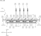
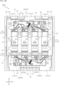
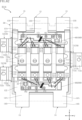
- FIG. 1 is a perspective view showing a semiconductor module according to a first embodiment.
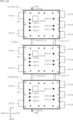
- FIG. 2 is a plan view showing the semiconductor module according to the first embodiment.
- FIG. 3 is a diagram showing the sealing portion with imaginary lines in the plan view of FIG. 2.
- FIG. 4 is a plan view of the main part of FIG. 3.
- FIG. 5 is a bottom view showing the semiconductor module according to the first embodiment.
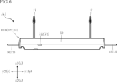
- FIG. 6 is a front view showing the semiconductor module according to the first embodiment.
- FIG. 7 is a rear view of the semiconductor module according to the first embodiment.
- FIG. 8 is a left side view showing the semiconductor module according to the first embodiment.
- FIG. 9 is a right side view showing the semiconductor module according to the first embodiment.
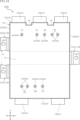
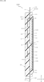
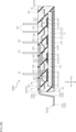
- FIG. 10 is a perspective view showing a semiconductor device (second device) of the semiconductor module according to the first embodiment.
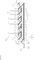
- FIG. 11 is a plan view showing the semiconductor device (second device) of the semiconductor module according to the first embodiment.
- FIG. 12 is a diagram showing the sealing portion with imaginary lines in the plan view of FIG. 11.
- FIG. 13 is a plan view of FIG. 12 in which the sealing portion and the second conductive member are omitted.
- FIG. 14 is a plan view of FIG. 13 with the first conductive member omitted.
- FIG. 15 is a bottom view showing the semiconductor device (second device) of the semiconductor module according to the first embodiment.
- FIG. 16 is a sectional view taken along line XIV-XIV in FIG. 12.
- FIG. 17 is a partially enlarged sectional view of a part of FIG.
- FIG. 16 is near the first element.
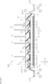
- FIG. 18 is a partially enlarged sectional view of a part of FIG. 16 (near the second element).
- FIG. 19 is a cross-sectional view taken along line XIX-XIX in FIG. 12.
- FIG. 20 is a cross-sectional view taken along line XX-XX in FIG. 12.
- FIG. 21 is a sectional view taken along line XXI-XXI in FIG. 12.
- 22 is a sectional view taken along line XXII-XXII in FIG. 12.
- FIG. 23 is a sectional view taken along line XXIII-XXIII in FIG. 12.
- FIG. 24 is a plan view showing the mounting structure of the semiconductor module according to the first embodiment.
- FIG. 25 is a plan view of FIG.
- FIG. 26 is a front view showing the semiconductor module mounting structure according to the first embodiment.
- FIG. 27 is a left side view showing the mounting structure for the semiconductor module according to the first embodiment.
- FIG. 28 is a partially enlarged sectional view of the semiconductor module mounting structure according to the first embodiment.
- FIG. 29 is a plan view showing a semiconductor module and a mounting structure for the semiconductor module according to a first modification of the first embodiment.
- FIG. 30 is a left side view showing a semiconductor module and a mounting structure for the semiconductor module according to the first modification of the first embodiment.
- FIG. 31 is a cross-sectional view showing a semiconductor module according to a second modification of the first embodiment, and corresponds to the cross-section of FIG. 23.
- FIG. 32 is a plan view showing a semiconductor module according to the second embodiment.
- FIG. 33 is a plan view of essential parts of a semiconductor module according to the second embodiment.
- FIG. 34 is a sectional view of a main part of a semiconductor module according to a second embodiment.
- FIG. 35 is a plan view of main parts showing a semiconductor module according to a modification of the second embodiment.
- FIG. 36 is a sectional view of a main part of a semiconductor module according to a modification of the second embodiment, and corresponds to the cross section of FIG. 21.
- FIG. 37 is a sectional view of a main part of a semiconductor module according to a modification of the second embodiment, and corresponds to the cross section of FIG. 22.
- FIG. 38 is a plan view showing a semiconductor module according to the third embodiment.
- FIG. 39 is a plan view showing a semiconductor module according to the fourth embodiment.
- FIG. 40 is a plan view showing a semiconductor module according to a first modification of the fourth embodiment.
- FIG. 41 is a plan view showing a semiconductor module according to a second modification of the fourth embodiment.
- FIG. 42 is a plan view showing an example of the configuration when the configuration of the second strip portion of the fourth embodiment is applied to the semiconductor module according to the second embodiment.
- FIG. 43 is a perspective view showing a semiconductor device according to the fifth embodiment.
- FIG. 44 is a plan view showing a semiconductor device according to the fifth embodiment.
- FIG. 45 is a diagram showing the sealing resin with imaginary lines in the plan view of FIG. 44.
- FIG. 46 is a partially enlarged view of FIG. 45.
- FIG. 45 is a diagram showing the sealing resin with imaginary lines in the plan view of FIG. 44.
- FIG. 47 is a diagram in which the second conductive member, the sealing resin, and the plate are omitted from the plan view of FIG. 45, and the first conductive member is shown in imaginary lines.
- FIG. 48 is a right side view showing the semiconductor device according to the fifth embodiment.
- FIG. 49 is a bottom view of the semiconductor device according to the fifth embodiment.
- FIG. 50 is a sectional view taken along line LL in FIG. 45.
- FIG. 51 is a sectional view taken along the LI-LI line in FIG. 45.
- FIG. 52 is a partially enlarged view of the first element shown in FIG. 51 and its surroundings.
- FIG. 53 is a partially enlarged view of the second element shown in FIG. 51 and its surroundings.
- FIG. 54 is a cross-sectional view taken along the line LIV-LIV in FIG.
- FIG. 55 is a cross-sectional view taken along the LV-LV line in FIG. 45.
- FIG. 56 is a plan view of the semiconductor module of the present disclosure, showing a state in which the semiconductor device according to the fifth embodiment is attached to a heat sink.
- FIG. 57 is a front view of the semiconductor module shown in FIG. 56.
- FIG. 58 is a partially enlarged sectional view of the wiring board of the semiconductor module shown in FIG. 56.
- FIG. 59 is a plan view showing a semiconductor device according to the first modification of the fifth embodiment, in which the sealing resin is shown with imaginary lines.
- FIG. 60 is a cross-sectional view of a semiconductor device according to a second modification of the fifth embodiment, and corresponds to the cross-section of FIG. 54.
- FIG. 60 is a cross-sectional view of a semiconductor device according to a second modification of the fifth embodiment, and corresponds to the cross-section of FIG. 54.
- FIG. 61 is a cross-sectional view showing a semiconductor device according to a third modification of the fifth embodiment, and corresponds to the cross-section of FIG. 54.
- FIG. 62 is a plan view showing a semiconductor device according to a fourth modification of the fifth embodiment, in which a sealing resin is shown with imaginary lines.
- FIG. 63 is a cross-sectional view showing a semiconductor device according to a fifth modification of the fifth embodiment, and corresponds to the cross-section of FIG. 54.
- FIG. 64 is a plan view showing the semiconductor device according to the sixth embodiment, in which the sealing resin is shown with imaginary lines.
- FIG. 65 is a cross-sectional view showing the semiconductor device according to the sixth embodiment, and corresponds to the cross-section of FIG. 54.
- FIG. 66 is a cross-sectional view showing the semiconductor device according to the sixth embodiment, and corresponds to the cross-section of FIG. 55.
- FIG. 67 is a cross-sectional view showing the semiconductor device according to the seventh embodiment, and corresponds to the cross-section of FIG. 54.
- FIG. 68 is a cross-sectional view showing the semiconductor device according to the seventh embodiment, and corresponds to the cross-section of FIG. 55.
- FIGS. 1 to 42 Preferred embodiments of the semiconductor module and semiconductor module mounting structure of the present disclosure will be described below with reference to FIGS. 1 to 42.
- the same or similar components will be denoted by the same reference numerals, and redundant explanation will be omitted.
- Terms such as “first”, “second”, “third”, etc. in this disclosure are used merely as labels and are not necessarily intended to attach a permutation to those objects.
- preferred embodiments of semiconductor devices and semiconductor modules according to other aspects of the present disclosure will be described below with reference to FIGS. 43 to 68.
- the symbols used in FIGS. 1 to 42 (first to fourth embodiments) and the symbols used in FIGS. 43 to 68 are independent from each other.
- the same reference numerals may be used for different members (elements, etc.), and different reference numerals may be used for the same (or similar) members (elements, etc.).
- a thing A is formed on a thing B" and "a thing A is formed on a thing B” mean “a thing A is formed on a thing B" unless otherwise specified.
- A is formed directly on something B
- a thing A is formed on something B, with another thing interposed between them.” including.
- "a certain thing A is placed on a certain thing B” and "a certain thing A is placed on a certain thing B” are used as "a certain thing A is placed on a certain thing B” unless otherwise specified.
- ⁇ It is placed directly on something B,'' and ⁇ A thing A is placed on something B, with another thing interposed between them.'' include.
- an object A is located on an object B
- an object A is in contact with an object B, and an object A is located on an object B.
- an object A overlaps an object B when viewed in a certain direction means, unless otherwise specified, “an object A overlaps all of an object B" and "a certain object A overlaps an object B".
- a certain thing A (the material of the thing) includes a certain material C” means "a case where the thing A (the material of the thing A) consists of a certain material C" and "the main component of the thing A (the material of the thing)”. "is a certain material C”.
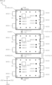
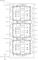
- the semiconductor module A1 is used, for example, as an inverter for driving a three-phase AC motor.
- the semiconductor module A1 includes a plurality of semiconductor devices B1, a connecting portion 71, and an extending portion 72.
- the semiconductor module A1 includes three semiconductor devices B1, but the number of semiconductor devices B1 is not limited to three.
- the semiconductor module A1 constitutes a full bridge circuit, it includes two semiconductor devices B1.
- the thickness direction z corresponds to the thickness direction of the semiconductor module A1.
- plane view refers to when viewed in the thickness direction z.
- the first direction x is orthogonal to the thickness direction z.
- the second direction y is orthogonal to the thickness direction z and the first direction x. Note that one side of the first direction x will be referred to as the x1 side of the first direction x, and the other side of the first direction x will be referred to as the x2 side of the first direction x.
- the plurality of semiconductor devices B1 are arranged at intervals along the first direction x. This interval may be the same or different for each of the two semiconductor devices B1 adjacent in the first direction x.
- Each of the plurality of semiconductor devices B1 includes a plurality of power terminals 13, a plurality of signal terminals 17, a plurality of semiconductor elements 21, and a sealing part 50, as shown in FIGS. 1 to 9.
- the plurality of semiconductor elements 21 are covered with a sealing portion 50.
- the plurality of power terminals 13 protrude from the side surface of the sealing part 50 in the second direction y.
- the plurality of signal terminals 17 protrude from the upper surface (top surface 51 described below) of the sealing portion 50 in the thickness direction z. Note that a detailed configuration example of each semiconductor device B1 will be described later.
- the plurality of semiconductor devices B1 include a first outer device B21 and a second outer device B22.
- the first outer device B21 is located at the outermost position on the x1 side in the first direction x among the plurality of semiconductor devices B1.
- the first outer device B21 corresponds to the first device B11.
- the second outer device B22 is located at the outermost position on the x2 side in the first direction x among the plurality of semiconductor devices B1.
- the second outer device B22 corresponds to the third device B13.
- the first strip portion 711 is electrically connected to each of the plurality of semiconductor elements 21 of each of the plurality of semiconductor devices B1.
- the first strip portion 711 of the first connecting portion 71A connects one of the plurality of power terminals 13 of the first device B11 (second power terminal 15 described later) and one of the plurality of power terminals 13 of the second device B12. (a second power terminal 15 to be described later).
- the first strip portion 711 of the second connecting portion 71B connects one of the plurality of power terminals 13 of the second device B12 (second power terminal 15 described below) and one of the plurality of power terminals 13 of the third device B13. (a second power terminal 15 to be described later).
- the second strip portion 712 is not electrically connected to any of the plurality of semiconductor elements 21 of each of the plurality of semiconductor devices B1 (non-conductive). As shown in FIG. 4, the second strip portion 712 includes a covering portion 7121, a covering portion 7122, and an exposed portion 7123 in each of the first connecting portion 71A and the second connecting portion 71B.
- the extending portion 72 is not electrically connected to any of the plurality of semiconductor elements 21 of each of the plurality of semiconductor devices B1 (non-conductive). As shown in FIGS. 2 to 4, the extension section 72 has a first extension section 721 and a second extension section 722.
- the first extending portion 721 protrudes from the first outer device B21 (first device B11) toward the x1 side in the first direction x.
- the first extending portion 721 has a band shape whose longitudinal direction is the first direction x.
- the first extending portion 721 includes a covering portion 7211 and an exposed portion 7212.
- the covering portion 7211 is covered by the sealing portion 50 of the first device B11.
- the exposed portion 7212 is connected to the covering portion 7211 and exposed from the sealing portion 50 of the first device B11.
- the second extending portion 722 protrudes from the second outer device B22 (third device B13) toward the x2 side in the first direction x.
- the second extending portion 722 has a band shape whose longitudinal direction is in the first direction x.
- the second extending portion 722 includes a covering portion 7221 and an exposed portion 7222.
- the covering portion 7221 is covered by the sealing portion 50 of the third device B13.
- the exposed portion 7222 is connected to the covering portion 7221 and exposed from the sealing portion 50 of the third device B13.
- the first extending portion 721 has a first through hole 7210.
- the first through hole 7210 is formed in an exposed portion 7212 of the first extending portion 721 .
- the first through hole 7210 penetrates the first extending portion 721 in the thickness direction z.
- the second extending portion 722 has a second through hole 7220.
- the second through hole 7220 is formed in the exposed portion 7222 of the second extending portion 722 .
- the second through hole 7220 penetrates the second extending portion 722 in the thickness direction z.
- either or both of the third through hole 710 of the first connecting portion 71A and the third through hole 710 of the second connecting portion 71B may be opened in a perfect circle in plan view.
- the opening shapes of the first through hole 7210, the second through hole 7220, and each third through hole 710 of the first connecting portion 71A and the second connecting portion 71B in plan view are a perfect circle or a long hole. It may be either.
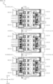
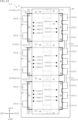
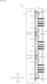
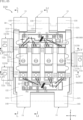
- each semiconductor device B1 (each of the first device B11, second device B12, and third device B13) includes a support substrate 11, a plurality of power terminals 13, a plurality of signal terminals 17, It includes a plurality of semiconductor elements 21, a thermistor 22, a first conductive member 31, a second conductive member 32, a plurality of wires, a sealing part 50, and a pair of control wiring 60.
- the plurality of power terminals 13 include a first power terminal 14, two second power terminals 15, and two third power terminals 16, and the plurality of signal terminals 17 include a first signal terminal 171, a second signal terminal 172, It includes a third signal terminal 173, a fourth signal terminal 174, a fifth signal terminal 181, and a pair of sixth signal terminals 182.
- the plurality of wires include a plurality of first wires 41, a plurality of second wires 42, a plurality of third wires 43, and a plurality of fourth wires 44.
- Each semiconductor device B1 converts the DC power supply voltage applied to the first power terminal 14 and the two second power terminals 15 into AC power using the plurality of semiconductor elements 21.
- the converted AC power is input from the two third power terminals 16 to a power supply target such as a motor.
- the support substrate 11 supports a plurality of semiconductor elements 21 in the thickness direction z, as shown in FIGS. 14, 16 to 19, 21, and 22.
- the support substrate 11 is composed of, for example, a DBC (Direct Bonded Copper) substrate.
- the support substrate 11 includes an insulating layer 111, a first wiring layer 112, and a second wiring layer 113.
- the support substrate 11 is covered with a sealing part 50 except for a part of the second wiring layer 113.
- the insulating layer 111 includes a portion interposed between the first wiring layer 112 and the second wiring layer 113 in the thickness direction z.
- the insulating layer 111 is made of a material with relatively high thermal conductivity.
- the insulating layer 111 is made of ceramics containing aluminum nitride (AlN), for example.
- the insulating layer 111 may be made of an insulating resin sheet instead of ceramics.
- the first wiring layer 112 is located above the insulating layer 111 (on the z1 side) in the thickness direction z.
- the composition of the first wiring layer 112 includes copper (Cu).
- the first wiring layer 112 is surrounded by the periphery of the insulating layer 111 in plan view.
- the first wiring layer 112 includes a first mounting section 1121 and a second mounting section 1122.
- the first mounting section 1121 and the second mounting section 1122 each have a rectangular shape in plan view.
- the first mounting section 1121 and the second mounting section 1122 are separated from each other in the second direction y.
- Each of the plurality of semiconductor elements 21 is bonded to either the first mounting section 1121 or the second mounting section 1122.
- the second wiring layer 113 is located below the insulating layer 111 (on the z2 side) in the thickness direction z. As shown in FIG. 15, the second wiring layer 113 is exposed from the sealing part 50. A heat sink 80, which will be described later, is bonded to the second wiring layer 113.
- the composition of the second wiring layer 113 includes copper.
- the second wiring layer 113 has a rectangular shape in plan view.
- the second wiring layer 113 is surrounded by the periphery of the insulating layer 111 in plan view.
- Each of the plurality of semiconductor elements 21 is mounted on either the first mounting section 1121 or the second mounting section 1122, as shown in FIG. 14 and FIGS. 16 to 19.
- Each semiconductor element 21 is, for example, a MOSFET (Metal-Oxide-Semiconductor Field-Effect Transistor).
- each semiconductor element 21 may be a switching element such as an IGBT (Insulated Gate Bipolar Transistor) or a diode.
- the semiconductor element 21 is an n-channel type MOSFET with a vertical structure.
- Semiconductor element 21 includes a compound semiconductor substrate.
- the composition of the compound semiconductor substrate includes silicon carbide (SiC) or silicon (Si).
- the plurality of semiconductor elements 21 include a plurality of first elements 21A and a plurality of second elements 21B.
- the structure of each of the plurality of second elements 21B is the same as the structure of each of the plurality of first elements 21A.
- the plurality of first elements 21A are mounted on the first mounting section 1121.
- the plurality of first elements 21A are arranged along the first direction x.
- the plurality of second elements 21B are mounted on the second mounting section 1122.
- the plurality of second elements 21B are arranged along the first direction x.
- the plurality of semiconductor elements 21 have a first electrode 211, a second electrode 212, a third electrode 213, and two fourth electrodes 214.
- the first electrode 211 faces either the first mounting section 1121 or the second mounting section 1122.
- a current corresponding to the power before being converted by the semiconductor element 21 flows through the first electrode 211 . That is, the first electrode 211 corresponds to the drain electrode of the semiconductor element 21.
- the second electrode 212 is located on the opposite side from the first electrode 211 in the thickness direction z. A current corresponding to the power converted by the semiconductor element 21 flows through the second electrode 212 . That is, the second electrode 212 corresponds to the source electrode of the semiconductor element 21.
- the third electrode 213 is located on the same side as the second electrode 212 in the thickness direction z.
- a gate voltage for driving the semiconductor element 21 is applied to the third electrode 213 . That is, the third electrode 213 corresponds to the gate electrode of the semiconductor element 21.
- the area of the third electrode 213 is smaller than the area of the second electrode 212 in plan view.
- the two fourth electrodes 214 are located on the same side as the second electrode 212 in the thickness direction z, and adjacent to the third electrode 213 in the first direction x. Located in In the illustrated example, the two fourth electrodes 214 are arranged on both sides of the third electrode 213 with the third electrode 213 in between in the first direction x. The potential of each fourth electrode 214 is equal to the potential of the second electrode 212. Unlike the illustrated example, each semiconductor element 21 may include only one of the two fourth electrodes 214 or may not include either of the two fourth electrodes 214.
- the conductive bonding layer 23 is interposed between either the first mounting portion 1121 or the second mounting portion 1122 and the first electrode 211 of any one of the plurality of semiconductor elements 21. ing.
- the conductive bonding layer 23 is, for example, solder.
- the conductive bonding layer 23 may include a sintered body of metal particles.
- the first electrodes 211 of the plurality of first elements 21A are electrically bonded to the first mounting portion 1121 via the electrically conductive bonding layer 23. Thereby, the first electrodes 211 of the plurality of first elements 21A are electrically connected to the first mounting portion 1121.
- the first electrodes 211 of the plurality of second elements 21B are electrically bonded to the second mounting portion 1122 via the electrically conductive bonding layer 23. Thereby, the first electrodes 211 of the plurality of second elements 21B are electrically connected to the second mounting portion 1122.
- the plurality of power terminals 13 are electrically connected to the plurality of semiconductor elements 21, respectively. A current corresponding to the power before being converted by the plurality of semiconductor elements 21 or a current corresponding to the power after being converted by the plurality of semiconductor elements 21 flows through the plurality of power terminals 13 .
- the plurality of power terminals 13 include a first power terminal 14 , two second power terminals 15 , and two third power terminals 16 .
- the first power terminal 14 is joined to the first mounting portion 1121, as shown in FIGS. 13 and 19. This joining is not limited in any way, and may be performed using a conductive joining material (for example, solder), which is not shown, or by laser welding, or by caulking.
- the first power terminal 14 is electrically connected to the first electrodes 211 of the plurality of first elements 21A via the first mounting portion 1121.
- the first power terminal 14 is a P terminal (positive electrode) to which a DC power supply voltage to be subjected to power conversion is applied. As shown in FIG. 13, the first power terminal 14 is located on the opposite side of the second mounting portion 1122 with the first mounting portion 1121 interposed therebetween in the second direction y.
- the first power terminal 14 extends from the first mounting portion 1121 to one side (y1 side) in the second direction y, and projects from the sealing portion 50 to one side (y1 side) in the second direction y. As shown in FIG. 12, the first power terminal 14 includes a portion covered by the sealing portion 50 and a portion exposed from the sealing portion 50. A portion of the first power terminal 14 covered by the sealing portion 50 is joined to the first mounting portion 1121 . Further, the portion of the first power terminal 14 exposed from the sealing portion 50 is used as the above-mentioned P terminal of each semiconductor device B1.
- a second conductive member 32 is connected to the two second power terminals 15.
- the two second power terminals 15 are electrically connected to the second electrodes 212 of the plurality of second elements 21B via the second conductive member 32.
- the two second power terminals 15 are N terminals (negative electrodes) to which a DC power supply voltage to be subjected to power conversion is applied.
- the two second power terminals 15 are separated from each other in the first direction x.
- the first power terminal 14 is located between the two second power terminals 15 . As shown in FIG. 13, the two second power terminals 15 are each located on the same side as the first power terminal 14 with respect to the first mounting portion 1121 and the second mounting portion 1122 in the second direction y.
- the two second power terminals 15 are separated from the first mounting section 1121 and the second mounting section 1122, respectively.
- the two second power terminals 15 each extend in the second direction y, and protrude from the sealing portion 50 to one side (y1 side) in the second direction y.
- each of the two second power terminals 15 includes a portion covered by the sealing portion 50 and a portion exposed from the sealing portion 50.
- a second conductive member 32 is joined to a portion of each second power terminal 15 covered by the sealing portion 50 . Further, in each second power terminal 15, the portion exposed from the sealing portion 50 is used as the aforementioned N terminal of each semiconductor device B1.
- the first strip portion 711 of the first connection portion 71A described above connects the second power terminal 15 on the x2 side of the two second power terminals 15 of the first device B11 and the two second power terminals of the second device B12. It is connected to the second power terminal 15 on the x1 side among the terminals 15 and is formed integrally therewith.
- the first strip portion 711 of the second connection portion 71B described above connects the second power terminal 15 on the x2 side of the two second power terminals 15 of the second device B12 and the two second power terminals of the third device B13. It is connected to the second power terminal 15 on the x1 side among the terminals 15.
- the two third power terminals 16 are each joined to the second mounting portion 1122, as shown in FIGS. 13 and 16. This joining is not limited in any way, and may be performed using a conductive joining material (for example, solder), which is not shown, or by laser welding, or by caulking.
- the two third power terminals 16 are electrically connected to the first electrodes 211 of the plurality of second elements 21B via the second mounting portions 1122, respectively. Further, the two third power terminals 16 are electrically connected to the second electrodes 212 of the plurality of first elements 21A via the second mounting portion 1122 and the first conductive member 31, respectively.
- AC power converted by the plurality of semiconductor elements 21 (the plurality of first elements 21A and the plurality of second elements 21B) is output from the two third power terminals 16.
- each of the two third power terminals 16 is an output terminal for the AC power.
- the two third power terminals 16 are separated from each other in the first direction x.
- the two third power terminals 16 are each located on the opposite side of the first mounting section 1121 with the second mounting section 1122 interposed therebetween in the second direction y.
- the two third power terminals 16 each extend from the second mounting portion 1122 to the other side (y2 side) in the second direction y, and protrude from the sealing portion 50 to the other side (y2 side) in the second direction y.
- each of the two third power terminals 16 includes a portion covered by the sealing portion 50 and a portion exposed from the sealing portion 50. In each third power terminal 16 , a portion covered by the sealing portion 50 is joined to the second mounting portion 1122 . Further, in each third power terminal 16, the portion exposed from the sealing portion 50 is used as the above-mentioned output terminal of each semiconductor device B1.
- the pair of control wires 60 constitute part of a conductive path between the plurality of signal terminals 17 and the plurality of semiconductor elements 21.
- the pair of control wirings 60 includes a first wiring 601 and a second wiring 602.
- the first wiring 601 is located between the plurality of first elements 21A, the first power terminal 14, and the two second power terminals 15 in the second direction y.
- the first wiring 601 is joined to the first mounting portion 1121, as shown in FIG.
- the second wiring 602 is located between the plurality of second elements 21B and the two third power terminals 16 in the second direction y.
- the second wiring 602 is joined to the second mounting portion 1122, as shown in FIG.
- the pair of control wirings 60 includes an insulating layer 61 , a plurality of wiring layers 62 , a metal layer 63 and a plurality of sleeves 64 .
- the pair of control wires 60 are covered with the sealing portion 50 except for a portion of each of the plurality of sleeves 64 .
- the insulating layer 61, multiple wiring layers 62, metal layers 63, and multiple sleeves 64 described below are common to the pair of control wiring 60 (first wiring 601 and second wiring 602) unless otherwise specified. .
- the plurality of wiring layers 62 are located above the insulating layer 61 in the thickness direction z (on the z1 side).
- the composition of the plurality of wiring layers 62 includes copper.
- the plurality of wiring layers 62 include a first wiring layer 621, a second wiring layer 622, a third wiring layer 623, a fourth wiring layer 624, and a fifth wiring layer 625.
- the metal layer 63 is located on the opposite side from the plurality of wiring layers 62 with the insulating layer 61 in between in the thickness direction z.
- the composition of metal layer 63 includes copper.
- the metal layer 63 of the first wiring 601 is bonded to the first mounting portion 1121 by an adhesive layer (not shown).
- the metal layer 63 of the second wiring 602 is bonded to the second mounting portion 1122 by an adhesive layer (not shown).
- These adhesive layers are made of materials that may or may not be electrically conductive. For example, these adhesive layers are solder.
- each of the plurality of sleeves 64 is bonded to one of the plurality of wiring layers 62 by a conductive bonding layer (for example, solder) not shown.
- the plurality of sleeves 64 are made of a conductive material such as metal.
- Each of the plurality of sleeves 64 has a cylindrical shape extending along the thickness direction z.
- One end of the plurality of sleeves 64 (the edge on the z2 side in the thickness direction z) is electrically conductively bonded to one of the plurality of wiring layers 62.
- the other ends of the plurality of sleeves 64 are exposed from the sealing part 50.
- the thermistor 22 straddles the third wiring layer 623 of the second wiring 602 and the fifth wiring layer 625 of the second wiring 602 and is electrically bonded to them.
- the thermistor 22 is, for example, an NTC (Negative Temperature Coefficient) thermistor.
- the NTC thermistor has a characteristic that its resistance gradually decreases as the temperature rises.
- the thermistor 22 is used as a temperature detection sensor of the semiconductor device B1.
- each of the plurality of signal terminals 17 is made of a metal pin extending in the thickness direction z.
- the plurality of signal terminals 17 protrude from a top surface 51 of the sealing portion 50, which will be described later.
- the plurality of signal terminals 17 are individually press-fitted into the plurality of sleeves 64 of the pair of control wirings 60. Thereby, each of the plurality of signal terminals 17 is supported by one of the plurality of sleeves 64 and is electrically connected to any one of the plurality of wiring layers 62.
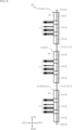
- the plurality of signal terminals 17 include a first signal terminal 171 , a second signal terminal 172 , a third signal terminal 173 , a fourth signal terminal 174 , a fifth signal terminal 181 , and a pair of sixth signal terminals 182 .
- the first signal terminal 171 , the second signal terminal 172 , the third signal terminal 173 , the fourth signal terminal 174 , and the fifth signal terminal 181 are electrically connected to any one of the plurality of semiconductor elements 21 .
- the pair of sixth signal terminals 182 are not electrically connected to any of the plurality of semiconductor elements 21 (non-conductive).
- the first signal terminal 171 is press-fitted into the sleeve 64, which is joined to the first wiring layer 621 of the first wiring 601, among the plurality of sleeves 64. Thereby, the first signal terminal 171 is supported by the sleeve 64 and electrically connected to the first wiring layer 621 of the first wiring 601. Further, the first signal terminal 171 is electrically connected to the third electrode 213 of the plurality of first elements 21A. A gate voltage for driving the plurality of first elements 21A is applied to the first signal terminal 171.
- the second signal terminal 172 is press-fitted into the sleeve 64, which is joined to the first wiring layer 621 of the second wiring 602, among the plurality of sleeves 64. Thereby, the second signal terminal 172 is supported by the sleeve 64 and is electrically connected to the first wiring layer 621 of the second wiring 602. Further, the second signal terminal 172 is electrically connected to the third electrode 213 of the plurality of second elements 21B. A gate voltage for driving the plurality of second elements 21B is applied to the second signal terminal 172.
- the third signal terminal 173 is located next to the first signal terminal 171 in the first direction x, as shown in FIGS. 14 and 20. As shown in FIG. 20, the third signal terminal 173 is press-fitted into one of the plurality of sleeves 64, which is joined to the second wiring layer 622 of the first wiring 601. Thereby, the third signal terminal 173 is supported by the sleeve 64 and is electrically connected to the second wiring layer 622 of the first wiring 601. Further, the third signal terminal 173 is electrically connected to the fourth electrode 214 of the plurality of first elements 21A. A voltage corresponding to the maximum current flowing through the fourth electrode 214 of each of the plurality of first elements 21A is applied to the third signal terminal 173.
- the fourth signal terminal 174 is located next to the second signal terminal 172 in the first direction x, as shown in FIGS. 14 and 23. As shown in FIG. 23, the fourth signal terminal 174 is press-fitted into one of the plurality of sleeves 64, which is joined to the second wiring layer 622 of the second wiring 602. Thereby, the fourth signal terminal 174 is supported by the sleeve 64 and electrically connected to the second wiring layer 622 of the second wiring 602. Further, the fourth signal terminal 174 is electrically connected to the fourth electrodes 214 of the plurality of second elements 21B. A voltage corresponding to the maximum current flowing through the fourth electrode 214 of each of the plurality of second elements 21B is applied to the fourth signal terminal 174.
- the fifth signal terminal 181 is located on the opposite side of the first signal terminal 171 with the third signal terminal 173 in between in the first direction x.
- the fifth signal terminal 181 is press-fitted into the sleeve 64 joined to the fifth wiring layer 625 of the first wiring 601, as shown in FIG. Thereby, the fifth signal terminal 181 is supported by the sleeve 64 and electrically connected to the fifth wiring layer 625 of the first wiring 601. Further, the fifth signal terminal 181 is electrically connected to the first mounting portion 1121.
- a voltage corresponding to the DC power input to the first power terminal 14 is applied to the fifth signal terminal 181 .
- the pair of sixth signal terminals 182 are located on the opposite side of the second signal terminal 172 with the fourth signal terminal 174 in between in the first direction x.
- the pair of sixth signal terminals 182 are adjacent to each other in the first direction x.
- the pair of sixth signal terminals 182 are individually press-fitted into a pair of sleeves 64 joined to the third wiring layer 623 of the second wiring 602 and the fifth wiring layer 625 of the second wiring 602, as shown in FIG. ing.
- the pair of sixth signal terminals 182 are individually supported by the pair of sleeves 64 and individually electrically connected to the third wiring layer 623 of the second wiring 602 and the fifth wiring layer 625 of the second wiring 602. are doing.
- the pair of sixth signal terminals 182 are electrically connected to the thermistor 22 .
- the plurality of first wires 41, the plurality of second wires 42, the plurality of third wires 43, and the fourth wires 44 each electrically connect mutually separated parts.
- the plurality of first wires 41, the plurality of second wires 42, the plurality of third wires 43, and the fourth wires 44 are each bonding wires. Note that in FIGS. 3, 4, 12, 16 to 20, and 23, the plurality of first wires 41, the plurality of second wires 42, the plurality of third wires 43, and the fourth wire 44 are omitted. .
- the plurality of first wires 41 are electrically connected to the third electrodes 213 of the plurality of first elements 21A and the fourth wiring layer 624 of the first wiring 601.
- the plurality of third wires 43 are electrically connected to the fourth wiring layer 624 of the first wiring 601 and the first wiring layer 621 of the first wiring 601.
- the first signal terminal 171 is electrically connected to the third electrode 213 of the plurality of first elements 21A.
- the compositions of the plurality of first wires 41 and the plurality of third wires 43 include gold (Au).
- the compositions of the plurality of first wires 41 and the plurality of third wires 43 may include copper or aluminum.
- the plurality of second wires 42 are conductively bonded to either one of the two fourth electrodes 214 of the plurality of first elements 21A and the second wiring layer 622 of the first wiring 601.
- the third signal terminal 173 is electrically connected to either of the two fourth electrodes 214 of the plurality of first elements 21A.
- the plurality of second wires 42 are conductively bonded to either one of the two fourth electrodes 214 of the plurality of second elements 21B and the second wiring layer 622 of the second wiring 602. .
- the fourth signal terminal 174 is electrically connected to either of the two fourth electrodes 214 of the plurality of second elements 21B.
- the composition of the plurality of second wires 42 includes gold.
- composition of the plurality of second wires 42 may include copper or aluminum. Note that when each semiconductor element 21 (each of the plurality of first elements 21A and the plurality of second elements 21B) does not include any of the two fourth electrodes 214, the plurality of second wires 42 One each is bonded to the second electrode 212 of the element 21.
- the fourth wire 44 is conductively bonded to the fifth wiring layer 625 of the first wiring 601 and the first mounting portion 1121.
- the fifth signal terminal 181 is electrically connected to the first electrodes 211 of the plurality of first elements 21A via the first mounting portion 1121.
- the composition of the fourth wire 44 includes gold.
- the composition of the fourth wire 44 may include copper or aluminum.
- the first conductive member 31 is electrically connected to the second electrodes 212 of the plurality of first elements 21A and the second mounting portion 1122, as shown in FIGS. 13 and 16. Thereby, the second electrodes 212 of the plurality of first elements 21A are electrically connected to the second mounting portion 1122.
- the composition of the first conductive member 31 includes copper.
- the first conductive member 31 is a metal clip. As shown in FIGS. 13 and 16, the first conductive member 31 includes a main body 311, a plurality of first joints 312, and a plurality of second joints 313.
- the main body part 311 constitutes the main part of the first conductive member 31. As shown in FIG. 13, the main body portion 311 extends in the first direction x. As shown in FIGS. 13 and 16, the main body portion 311 straddles between the first mounting portion 1121 and the second mounting portion 1122. As shown in FIG. 13, a plurality of through holes 310 are formed in the main body portion 311. Each of the plurality of through holes 310 passes through the main body portion 311 in the thickness direction z. The plurality of through holes 310 overlap between the first mounting section 1121 and the second mounting section 1122 in plan view. Thereby, when forming the sealing part 50, the sealing part 50 can easily flow downward in the thickness direction z of the main body part 311 (z2 side in the thickness direction z).
- each first joint portion 312 extends from the main body portion 311 toward the y1 side in the second direction y.
- the plurality of first joint parts 312 are divided into two from the main body part 311, but they do not need to be divided into two.
- the base end of each first joint portion 312 (the end connected to the main body portion 311) is bent downward in the thickness direction z (to the z2 side in the thickness direction z). Therefore, the tip of each first joint 312 (the end opposite to the side connected to the main body 311) is located below the main body 311 in the thickness direction z (on the z2 side in the thickness direction z). ) located in
- each second joint portion 313 extends from the main body portion 311 toward the y2 side in the second direction y.
- the base end of each second joint portion 313 (the end connected to the main body portion 311) is bent downward in the thickness direction z (to the z2 side in the thickness direction z). Therefore, the tip of each second joint 313 (the end opposite to the side connected to the main body 311) is located below the main body 311 in the thickness direction z (on the z2 side in the thickness direction z). ) located in
- the semiconductor device B1 further includes a first conductive bonding layer 33, as shown in FIGS.
- the first conductive bonding layer 33 is interposed between the second electrodes 212 of the plurality of first elements 21A and the plurality of first bonding portions 312.
- the first conductive bonding layer 33 conductively bonds the second electrodes 212 of the plurality of first elements 21A and the plurality of first bonding portions 312.
- the first conductive bonding layer 33 is, for example, solder.
- the first conductive bonding layer 33 may include a sintered body of metal particles.
- the semiconductor device B1 further includes a second conductive bonding layer 34.
- the second conductive bonding layer 34 is interposed between the second mounting portion 1122 and the second bonding portion 314.
- the second conductive bonding layer 34 conductively bonds the second mounting portion 1122 and the second bonding portion 314 together.
- the second conductive bonding layer 34 is, for example, solder.
- the second conductive bonding layer 34 may include a sintered body of metal particles.
- the second conductive member 32 is electrically connected to the second electrodes 212 of the plurality of second elements 21B and the two second power terminals 15. Thereby, the second electrodes 212 of the plurality of second elements 21B are electrically connected to the two second power terminals 15.
- the composition of the second conductive member 32 includes copper.
- the second conductive member 32 is a metal clip.
- the second conductive member 32 includes a pair of main body parts 321, a plurality of third joint parts 322, a pair of fourth joint parts 324, and a plurality of intermediate parts 326. , a plurality of cross beam portions 327, and a pair of hanging portions 328.
- the pair of main body parts 321 are located apart from each other in the first direction x.
- the pair of main body parts 321 extend in the second direction y.
- the pair of main body parts 321 are arranged parallel to the upper surface of the first mounting part 1121 and the upper surface of the second mounting part 1122.
- the pair of main body parts 321 are located further away from the first mounting part 1121 and the second mounting part 1122 than the main body part 311 of the first conductive member 31 is.
- the plurality of third joints 322 are individually joined to the second electrodes 212 of the plurality of second elements 21B.
- Each of the plurality of third joints 322 faces one of the second electrodes 212 of the plurality of second elements 21B.
- the plurality of third joint portions 322 extend from the plurality of intermediate portions 326 in the first direction x.
- the base end of each third joint portion 322 (the end connected to the intermediate portion 326) is bent downward in the thickness direction z (to the z2 side in the thickness direction z). Therefore, the tip of each third joint portion 322 (the end opposite to the side connected to the intermediate portion 326) is located below the intermediate portion 326 in the thickness direction z (on the z2 side in the thickness direction z). ) located in
- the pair of fourth joints 324 are individually joined to the two second power terminals 15. Each of the pair of fourth joints 324 faces a corresponding one of the two second power terminals 15.
- the plurality of horizontal beams 327 are arranged along the first direction x.
- the plurality of horizontal beam portions 327 include regions that individually overlap the plurality of first joint portions 312 of the first conductive member 31.
- both sides in the first direction x of the cross beam part 327 located at the center in the first direction x among the plurality of cross beam parts 327 are connected to the plurality of intermediate parts 326.
- Both sides of the remaining two cross beam portions 327 in the first direction x among the plurality of cross beam portions 327 are connected to one of the pair of main body portions 321 and one of the plurality of intermediate portions 326.
- the pair of hanging parts 328 are individually connected to the pair of main body parts 321. As shown in FIG. 21, each of the pair of hanging parts 328 extends downward in the thickness direction z (z2 side in the thickness direction z) from a corresponding one of the pair of main body parts 321. Each of the pair of hanging parts 328 is connected to the outer edge of the corresponding one of the pair of main body parts 321 in the first direction x. In the illustrated example, the lower ends (edges on the z2 side in the thickness direction z) of the pair of hanging parts 328 overlap the first mounting part 1121 when viewed along the second direction y.
- the semiconductor device B1 further includes a third conductive bonding layer 35.
- the third conductive bonding layer 35 is interposed between the second electrodes 212 of the plurality of second elements 21B and the plurality of third bonding parts 322.
- the third conductive bonding layer 35 conductively bonds the second electrodes 212 of the plurality of second elements 21B and the plurality of third bonding parts 322.
- the third conductive bonding layer 35 is, for example, solder.
- the third conductive bonding layer 35 may include a sintered body of metal particles.
- the semiconductor device B1 further includes a fourth conductive bonding layer 36.
- the fourth conductive bonding layer 36 is interposed between the two second power terminals 15 and the pair of fourth bonding portions 324 .
- the fourth conductive bonding layer 36 conductively bonds the two second power terminals 15 and the pair of fourth bonding portions 324 .
- the fourth conductive bonding layer 36 is, for example, solder.
- the fourth conductive bonding layer 36 may include a sintered body of metal particles.
- the sealing section 50 includes a plurality of semiconductor elements 21, a first conductive member 31, a second conductive member 32, a plurality of first wires 41, a plurality of second wires 42, and a plurality of Cover the third wire 43. Furthermore, the sealing part 50 covers a portion of each of the support substrate 11 , the plurality of power terminals 13 , and the plurality of signal terminals 17 .
- the sealing portion 50 has electrical insulation properties.
- the sealing portion 50 includes, for example, black epoxy resin.
- the sealing portion 50 is formed by, for example, molding. As shown in FIGS. 10 to 12 and 15 to 23, the sealing portion 50 has a top surface 51, a bottom surface 52, a plurality of resin side surfaces 53, and a pair of recesses 55.
- the top surface 51 faces in the same direction as the top surface of the first mounting section 1121 and the top surface of the second mounting section 1122 in the thickness direction z.
- the bottom surface 52 faces opposite to the top surface 51 in the thickness direction z.
- the second wiring layer 113 of the support substrate 11 is exposed from the bottom surface 52.
- the plurality of resin side surfaces 53 are connected to the top surface 51.
- the plurality of resin side surfaces 53 include a pair of first side surfaces 531 and a pair of second side surfaces 532.
- the pair of first side surfaces 531 are located apart from each other in the second direction y.
- the pair of first side surfaces 531 face in the second direction y and extend in the first direction x.
- a pair of first side surfaces 531 are connected to the top surface 51.
- the first power terminal 14 and the two second power terminals 15 respectively protrude from the first side surface 531 on the y1 side in the second direction y of the pair of first side surfaces 531.
- Two third power terminals 16 each protrude from the first side surface 531 on the y2 side in the second direction y of the pair of first side surfaces 531.
- the first extending portion 721 is extended from the second side surface 532 on the x1 side of the pair of second side surfaces 532 of the first device B11. Stick out.
- the second strip portion 712 of the first connecting portion 71A mentioned above protrudes from the second side surface 532 on the x2 side of the pair of second side surfaces 532 of the first device B11, and It protrudes from the second side surface 532 of the second side surface 532 on the x1 side.
- the second strip portion 712 of the second connecting portion 71B mentioned above protrudes from the second side surface 532 on the x2 side of the pair of second side surfaces 532 of the second device B12, and also extends from the second side surface 532 of the second device B13.
- the pair of recesses 55 are recessed from the first side surface 531 of the pair of first side surfaces 531 on the y1 side in the second direction y toward the second direction y.
- the pair of recesses 55 extend from the top surface 51 to the bottom surface 52 in the thickness direction z.
- the pair of recesses 55 are located on both sides of the first power terminal 14 in the second direction y.
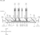
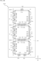
- the mounting structure C1 of the semiconductor module A1 includes the semiconductor module A1, a heat sink 80, a wiring board 81, a mounting member 84, a plurality of positioning pins 86, and a plurality of fastening members 87.
- the heat sink 80 supports the semiconductor module A1 (the plurality of semiconductor devices B1), as shown in FIGS. 26 and 27.
- the heat sink 80 is located on the opposite side of the plurality of semiconductor devices 21 of the plurality of semiconductor devices B1 from the plurality of signal terminals 17 of the plurality of semiconductor devices B1. Therefore, the heat sink 80 faces each second wiring layer 113 of the plurality of semiconductor devices B1.
- the heat sink 80 is made of a material containing aluminum, for example. As shown in FIGS. 24, 25, and 27, the plurality of semiconductor devices B1 are arranged on the heat sink 80 along the first direction x.
- the wiring board 81 is provided in common to the plurality of semiconductor devices B1, as shown in FIGS. 24 and 27. Unlike this configuration, a plurality of wiring boards 81 may be individually provided for a plurality of semiconductor devices B1. As understood from FIGS. 24 and 27, a plurality of signal terminals 17 of a plurality of semiconductor devices B1 are respectively inserted into the wiring board 81 and electrically connected to each signal terminal 17.
- the wiring board 81 is, for example, a gate driver that controls driving of each semiconductor element 21 of the plurality of semiconductor devices B1.
- the wiring board 81 faces the top surface 51 of each sealing section 50 of the plurality of semiconductor devices B1.
- the wiring board 81 is located on the opposite side of the heat sink 80 with respect to the plurality of semiconductor devices B1.
- the wiring board 81 individually overlaps each sealing part 50 of the plurality of semiconductor devices B1 in a plan view.
- FIG. 28 shows a state in which one of the signal terminals 17 of a plurality of semiconductor devices B1 is inserted into a through hole 811A of a substrate 811. Note that all the signal terminals 17 of the plurality of semiconductor devices B1 have the same configuration as shown in FIG. 28.
- each signal terminal 17 has a base 170A and a bulge 170B.
- One side of the base portion 170A in the thickness direction z is press-fitted into one of the plurality of sleeves 64 of the plurality of semiconductor devices B1.
- the bulging portion 170B is provided on one side (z1 side) of the base portion 170A in the thickness direction z.
- the bulging portion 170B bulges in a direction perpendicular to the thickness direction z.
- each signal terminal 17 is press-fitted into one of the plurality of through holes 811A of the wiring board 81.
- the internal wiring 814 placed in any one of the plurality of through holes 811A is pressed against the bulge 170B of the signal terminal 17 inserted through the through hole 811A. Therefore, each signal terminal 17 is electrically connected to the wiring board 81 by being press-fitted into the through hole 811A in the thickness direction z.
- the wiring board 81 is supported by each signal terminal 17 by press-fitting each signal terminal 17 into a corresponding one of the plurality of through holes 811A.
- each of the plurality of positioning pins 86 extends from the upper surface of the heat sink 80 (the surface facing the z1 side in the thickness direction z) to the z1 side in the thickness direction z.
- the plurality of positioning pins 86 may be integrally formed with the heat sink 80 or may be joined to the heat sink 80.
- the plurality of positioning pins 86 are respectively provided in the third through hole 710 of the second strip part 712 of the first connecting part 71A (connecting part 71) and the third through hole 710 of the second belt-like part 712 of the first connecting part 71A (connecting part 71).
- the tip of each positioning pin 86 (the edge on the z1 side in the thickness direction z) is in contact with the wiring board 81.
- the wiring board 81 is supported by the plurality of positioning pins 86.
- a plurality of pillars (not shown) may be arranged on the heat sink 80 or the sealing portion 50 of each semiconductor device B1, and the wiring board 81 may be supported by the plurality of pillars. In this case, the tip of each positioning pin 86 does not need to be in contact with the wiring board 81.
- the attachment member 84 is used to restrain the semiconductor module A1 (the plurality of semiconductor devices B1) to the heat sink 80, as shown in FIGS. 25 to 27.
- the composition of the attachment member 84 includes, for example, metal.
- the mounting member 84 contacts the top surface 51 of each sealing portion 50 of the plurality of semiconductor devices B1.
- the mounting member 84 straddles the top surface 51 of each sealing portion 50 of the plurality of semiconductor devices B1 in the first direction x.
- the mounting member 84 is, for example, a plate spring.
- the mounting member 84 is located between the first signal terminal 171 and the second signal terminal 172 of each semiconductor device B1 in the second direction y.
- the mounting member 84 is located between the heat sink 80 and the wiring board 81 in the thickness direction z.
- Attachment member 84 is partially bent.
- the mounting member 84 contacts the heat sink 80 between the two semiconductor devices B1 adjacent to each other in the first direction x. Furthermore, at least a part of the region of the mounting member 84 that overlaps each sealing portion 50 in plan view contacts the top surface 51 of each sealing portion 50 .
- a plurality of through holes 841 are formed in the mounting member 84 . Each of the plurality of through holes 841 penetrates the attachment member 84 in the thickness direction z. Each of the plurality of through holes 841 is formed in a portion of the mounting member 84 that contacts the heat sink 80 .
- Each of the plurality of fastening members 87 is, for example, a male thread. Each of the plurality of fastening members 87 is inserted into a corresponding one of the plurality of through holes 841, as shown in FIGS. 25 to 27. Each of the plurality of fastening members 87 is fastened to a female threaded hole (not shown) formed in the heat sink 80 . As a result, the plurality of semiconductor devices B1 are restrained by the mounting member 84 and the plurality of fastening members 87.
- the functions and effects of the semiconductor module A1 and the mounting structure C1 for the semiconductor module A1 are as follows.
- the semiconductor module A1 includes a plurality of semiconductor devices B1 and a connecting portion 71.
- the plurality of semiconductor devices B1 includes a first device B11 and a second device B12.
- the connecting portion 71 includes a first connecting portion 71A.
- the first connecting portion 71A is located between the first device B11 and the second device B12 in the first direction x, and connects the first device B11 and the second device B12. According to this configuration, it is possible to suppress variations in the relative positional relationship between the first device B11 and the second device B12 due to the first connecting portion 71A. Therefore, since the semiconductor module A1 can suppress variations in the position of the signal terminals 17 among the plurality of semiconductor devices B1, the wiring board 81 can be appropriately connected to the semiconductor module A1.
- the plurality of semiconductor devices B1 include a first device B11, a second device B12, and a third device B13.
- the connecting portion 71 includes a second connecting portion 71B.
- the second connecting portion 71B is located between the second device B12 and the third device B13 in the first direction x, and connects the second device B12 and the third device B13. According to this configuration, it is possible to suppress variations in the relative positional relationship between the second device B12 and the third device B13 due to the second connection portion 71B.
- the number of semiconductor devices B1 is not limited at all.
- the mounting structure C1 for the semiconductor module A1 includes the semiconductor module A1 and a heat sink 80.
- the semiconductor module A1 can suppress variations in the relative positional relationship of the plurality of semiconductor devices B1, according to the mounting structure C1 of the semiconductor module A1, the semiconductor module A1 can suppress the variation in the relative positional relationship of the plurality of semiconductor devices B1 with respect to the heat sink 80. Positioning accuracy can be improved.
- the semiconductor module A1 includes an extending portion 72.
- the extending portion 72 includes a first extending portion 721 that protrudes from the first outer device B21 toward the x1 side in the first direction x, and a second extending portion 721 that protrudes from the second outer device B22 toward the x2 side in the first direction x.
- the extension portion 722 is included.
- the first extending portion 721 has a first through hole 7210
- the second extending portion 722 has a second through hole 7220.
- the first through hole 7210 and the second through hole 7220 are each inserted into a corresponding one of the plurality of positioning pins 86 formed in the heat sink 80. According to this configuration, it is possible to suppress misalignment of the semiconductor module A1 with respect to the heat sink 80.
- the connecting portion 71 (each of the first connecting portion 71A and the second connecting portion 71B) includes a second strip portion 712.
- the second strip portion 712 of each of the first connecting portion 71A and the second connecting portion 71B has a third through hole 710.
- Each of the third through holes 710 is inserted into a corresponding one of the plurality of positioning pins 86 formed in the heat sink 80 . According to this configuration, misalignment of the semiconductor module A1 with respect to the heat sink 80 can be further suppressed.
- either the first through hole 7210 or the second through hole 7220 has a perfect circular opening when viewed in the thickness direction z.
- the second through hole 7220 opens in a perfect circle.
- the positioning pin 86 is inserted through the perfectly circular opening, thereby suppressing rotation and wobbling of the semiconductor module A1 along the xy plane.
- the other of the first through hole 7210 and the second through hole 7220 opens into a long hole when viewed in the thickness direction z.
- the first through hole 7210 opens into a long hole. This configuration suppresses connection failures of the wiring board 81 to the semiconductor module A1 due to manufacturing errors (manufacturing errors) of each semiconductor device B1.
- the first connection portion 71A includes a first strip portion 711.
- the first strip portion 711 connects the second power terminals 15 of the first device B11 and the second device B12 that are adjacent to each other in the first direction x. According to this configuration, the second power terminal 15 of the first device B11 and the second power terminal 15 of the second device B12 have the same potential.
- the second connecting portion 71B includes a first band-shaped portion 711. The first band-shaped portion 711 connects the second power terminals 15 of the second device B12 and the third device B13 that are adjacent to each other in the first direction x. According to this configuration, the second power terminal 15 of the second device B12 and the second power terminal 15 of the third device B13 have the same potential. For these reasons, the semiconductor module A1 can share the low potential side of the input power supply voltage.
- the connecting portion 71 includes a first connecting portion 71A and a second connecting portion 71B.
- Each of the first connecting portion 71A and the second connecting portion 71B includes a first strip portion 711 and a second strip portion 712.
- the first strip portion 711 is located closer to the y1 side in the second direction y than the second strip portion 712. According to this configuration, it is possible to further suppress variations in the positional relationship of the plurality of semiconductor devices B1.
- FIGS. 29 and 30 show a semiconductor module A11 according to a first modification of the first embodiment and a mounting structure C11 for the semiconductor module A11.
- the semiconductor module A11 differs from the semiconductor module A1 in the following points.
- Each of the second strip portions 712 of the first connecting portion 71A and the second connecting portion 71B of the connecting portion 71 has a portion bent downward in the thickness direction z. Further, the first extending portion 721 and the second extending portion 722 of the extending portion 72 are bent downward in the thickness direction z.
- the plurality of fastening members 87 each have a third through hole 710 in the first connecting portion 71A and a second connecting portion 71B, a first through hole 7210 in the first extending portion 721, and a first through hole 7210 in the first extending portion 721.
- the second extension portion 722 is inserted into a corresponding one of the second through holes 7220 of the second extension portion 722 . Thereby, the semiconductor module A11 is restrained by the heat sink 80.
- the mounting structure C11 for the semiconductor module A11 includes a plurality of supports 88.
- Each of the plurality of pillars 88 is located between the plurality of semiconductor devices B1 and the wiring board 81 in the thickness direction z.
- each of the plurality of pillars 88 is in contact with the top surface 51 of one of the sealing parts 50 of the plurality of semiconductor devices B1, and also in contact with the wiring board 81.
- four pillars 88 are arranged for each semiconductor device B1.
- the four pillars 88 are respectively arranged at the four corners of the region overlapping the wiring board 81 of the sealing portion 50 of the corresponding semiconductor device B1 in plan view.
- the constituent material of the plurality of pillars 88 may include either an insulating resin material or a metal material, but an insulating resin material is preferable in order to suppress unintended short circuits.
- the arrangement and number of the plurality of support columns 88 are not limited to the illustrated example.
- the plurality of support columns 88 may be arranged so as to contact the heat sink 80 instead of being arranged so as to contact the plurality of semiconductor devices B1.
- the semiconductor module A11 can suppress variations in the positional relationship of the plurality of semiconductor devices B1. Further, in the mounting structure C11 for the semiconductor module A11, the semiconductor module A11 is restrained to the heat sink 80 using the connecting portion 71 and the extension portion 72, so the mounting member 84 is not required. However, in order to securely restrain the semiconductor module A11 by the heat sink 80, the mounting structure C11 for the semiconductor module A11 may include a mounting member 84.
- FIG. 31 shows a semiconductor module A12 according to a second modification of the first embodiment.
- the semiconductor module A12 differs from the semiconductor module A1 in the following points. That is, each of the second strip portions 712 and the extension portions 72 (the first extension portion 721 and the second extension portion 722) of the connection portion 71 (the first connection portion 71A and the second connection portion 71B) are insulated. It is.
- each second strip portion 712, first extension portion 721, and second extension portion 722 each contain an insulating material.
- the insulating material is, for example, polycarbonate or glass epoxy resin. Since each of the second strip portions 712, the first extension portions 721, and the second extension portions 722 are insulative, they are joined to the second mounting portion 1122, as shown in FIG. 31.
- the semiconductor module A12 can suppress variations in the positional relationship of the plurality of semiconductor devices B1. Furthermore, in the semiconductor module A12, each of the second strip portions 712, the first extension portions 721, and the second extension portions 722 are bonded to the second mounting portions 1122 of the corresponding semiconductor devices B1, so that these are sealed. It is suppressed from coming off from the stop part 50.
- the semiconductor module A2 is different from the semiconductor module A1 in the configuration of each first strip portion 711 of the first connection portion 71A and the second connection portion 71B (connection portion 71). Note that the semiconductor module A2 is attached to the heat sink 80 similarly to the semiconductor module A1. That is, the mounting structure of the semiconductor module A2 is configured similarly to the mounting structure C1 of the semiconductor module A1.
- each first strip portion 711 is not electrically connected to any of the plurality of semiconductor elements 21 of each of the plurality of semiconductor devices B1.
- Each first strip portion 711 of the first connecting portion 71A and the second connecting portion 71B includes a covering portion 7111, a covering portion 7112, and an exposed portion 7113, as shown in FIG.
- the covering portion 7111 is covered with the sealing portion 50 of the first device B11, and the covering portion 7112 is covered with the sealing portion 50 of the second device B12. Further, the exposed portion 7113 is exposed from each of the sealing portion 50 of the first device B11 and the sealing portion 50 of the second device B12. The exposed portion 7113 is interposed between the covering portion 7111 and the covering portion 7112 in the first direction x.
- a third through hole 710 is formed in the exposed portion 7113. In the illustrated example, the third through hole 710 opens into a long hole in plan view, but may open into a perfect circle. As shown in FIG.
- the covering portion 7111 of the first connecting portion 71A is disposed between the support substrate 11 of the first device B11 and the main body portion 321 of the second conductive member 32 in the thickness direction z, and distance from.
- the covering portion 7111 extends until it overlaps the hanging portion 328 of the second conductive member 32 of the first device B11 when viewed along the second direction y.
- the covering portion 7112 of the first connecting portion 71A is arranged between the support substrate 11 of the second device B12 and the main body portion 321 of the second conductive member 32 in the thickness direction z, and is spaced apart from them.
- the covering portion 7112 extends until it overlaps the hanging portion 328 of the second conductive member 32 of the second device B12 when viewed along the second direction y.
- the covering portion 7111 is covered with the sealing portion 50 of the second device B12, and the covering portion 7112 is covered with the sealing portion 50 of the third device B13. Further, the exposed portion 7113 is exposed from each of the sealing portion 50 of the second device B12 and the sealing portion 50 of the third device B13. The exposed portion 7113 is interposed between the covering portion 7111 and the covering portion 7112 in the first direction x.
- a third through hole 710 is formed in the exposed portion 7113. In the illustrated example, the third through hole 710 opens into a long hole in plan view, but may open into a perfect circle.
- the positional relationship between the second connecting portion 71B, the second device B12, and the third device B13 is configured in the same manner as the positional relationship between the first connecting portion 71A, and the first device B11 and the second device B12.
- the covering portion 7111 of the second connecting portion 71B is located between the support substrate 11 of the second device B12 and the main body portion 321 of the second conductive member 32 in the thickness direction z. placed and separated from these.
- the covering portion 7111 extends until it overlaps the hanging portion 328 of the second conductive member 32 of the second device B12 when viewed along the second direction y.
- the covering portion 7112 of the second connecting portion 71B is arranged between the support substrate 11 of the third device B13 and the main body portion 321 of the second conductive member 32 in the thickness direction z, and is spaced apart from them.
- the covering portion 7112 extends until it overlaps the hanging portion 328 of the second conductive member 32 of the third device B13 when viewed along the second direction y.
- each second strip portion 712 has a partially large width inside the sealing portion 50, as shown in FIG. Thereby, each second band-shaped portion 712 can be prevented from coming off from the sealing portion 50.
- the covering portion 7211 of the first extending portion 721 and the covering portion 7221 of the second extending portion 722 have a larger width inside the sealing portion 50. Thereby, each of the first extension part 721 and the second extension part 722 can be prevented from coming off from the sealing part 50.
- the semiconductor module A2 can suppress variations in the positional relationship of the plurality of semiconductor devices B1. Furthermore, in the semiconductor module A2, as described above, each of the second strip portions 712, the first extension portions 721, and the second extension portions 722 is prevented from coming out of the sealing portion 50 of any one of the plurality of semiconductor devices B1. It can be suppressed. Further, in the semiconductor module A2, since the third through holes 710 are also formed in each of the first strip portions 711, the positioning pins 86 are inserted into the third through holes 710, so that the x- Rotation along the y-plane can be suppressed.
- 35 to 37 show a semiconductor module A21 according to a modification of the second embodiment.
- the semiconductor module A21 is different from the semiconductor module A2 in the configuration of the connecting portion 71 (first connecting portion 71A and second connecting portion 71B).
- the first strip portion 711 of the first connection portion 71A and the first strip portion 711 of the second connection portion 71B are connected to the sealing portion 50 of the second device B12. They are interconnected and integrally formed within the .
- this integrally formed part is referred to as the first band-shaped part 711 of the connecting part 71. Therefore, in this modification, the first strip portion 711 of the connecting portion 71 extends in the first direction x from one side to the other of the pair of second side surfaces 532 of the sealing portion 50 of the second device B12.
- the first strip portion 711 of the connecting portion 71 is located above the second conductive member 32 in the thickness direction z (on the z1 side in the thickness direction z). As shown in FIGS. 35 and 36, the first strip portion 711 of the connecting portion 71 overlaps the plurality of horizontal beam portions 327 and the plurality of first elements 21A in plan view. In the illustrated example, an insulating sheet 791 is disposed to prevent a short circuit between the first strip portion 711 of the connecting portion 71 and the second conductive member 32. The first strip portion 711 of the connecting portion 71 is placed on the second conductive member 32 with the insulating sheet 791 interposed therebetween.
- the insulating sheet 791 may not be provided.
- the first strip portion 711 of the first connecting portion 71A extends in the first direction x from one side to the other of the pair of second side surfaces 532 of the sealing portion 50 of the first device B11. It's okay.
- the first strip portion 711 of the second connecting portion 71B may extend in the first direction x from one side to the other of the pair of second side surfaces 532 of the sealing portion 50 of the third device B13.
- the second strip portion 712 of the first connection portion 71A and the second strip portion 712 of the second connection portion 71B are connected to the sealing portion 50 of the second device B12. They are interconnected and integrally formed within the .
- this integrally formed part is referred to as the second band-shaped part 712 of the connecting part 71. Therefore, in this modification, the second strip portion 712 of the connecting portion 71 extends in the first direction x from one side to the other of the pair of second side surfaces 532 of the sealing portion 50 of the second device B12.
- the second strip portion 712 of the connecting portion 71 is located above the second conductive member 32 in the thickness direction z (on the z1 side in the thickness direction z). As shown in FIGS. 35 and 37, the second strip portion 712 of the connecting portion 71 overlaps the plurality of third joint portions 322 and the plurality of second elements 21B in plan view. In the illustrated example, an insulating sheet 792 is disposed to prevent a short circuit between the second strip portion 712 of the connecting portion 71 and the second conductive member 32. The second strip portion 712 of the connecting portion 71 is placed on the second conductive member 32 with an insulating sheet 792 interposed therebetween.
- the insulating sheet 792 may not be provided. Furthermore, unlike the example shown in FIG. 37, the insulating sheet 792 may be separated into a plurality of parts and disposed only in the region in contact with the second conductive member 32.
- the second strip portion 712 of the first connecting portion 71A may extend in the first direction x from one side to the other of the pair of second side surfaces 532 of the sealing portion 50 of the first device B11. . In this case, the second strip portion 712 of the first connecting portion 71A is connected to the first extending portion 721 inside the sealing portion 50 of the first device B11.
- the second strip portion 712 of the second connecting portion 71B may extend in the first direction x from one side to the other of the pair of second side surfaces 532 of the sealing portion 50 of the third device B13.
- the second strip portion 712 of the second connecting portion 71B is connected to the second extending portion 722 inside the sealing portion 50 of the third device B13.
- the semiconductor module A21 can suppress variations in the positional relationship of the plurality of semiconductor devices B1.
- the semiconductor module A21 even if the first strip portion 711 of the aforementioned connecting portion 71 and the second strip portion 712 of the aforementioned connecting portion 71 are integrally formed, and the connecting portion 71 is a single wide plate material. good. Further, the first strip portion 711 of the aforementioned connecting portion 71 and the second strip portion 712 of the aforementioned connecting portion 71 may each be insulating.
- first connecting portion 71A and the second connecting portion 71B each include the first strip portion 711 and the second strip portion 712.
- each of the first connecting portion 71A and the second connecting portion 71B may include only one of the first strip portion 711 and the second strip portion 712.
- FIG. 38 shows a semiconductor module A3 according to the third embodiment.
- the semiconductor module A3 is different from the semiconductor module A2 in the configuration of the connecting portion 71 (the first connecting portion 71A and the second connecting portion 71B). Note that the semiconductor module A3 is attached to the heat sink 80 similarly to the semiconductor module A1. In other words, the mounting structure of the semiconductor module A3 is configured similarly to the mounting structure C1 of the semiconductor module A1.
- the first connecting portion 71A is integrally formed with the sealing portion 50 of the first device B11 and the sealing portion 50 of the second device B12. As shown in FIG. 38, two third through holes 710 are formed in the first connecting portion 71A. The two third through holes 710 penetrate the first connecting portion 71A in the thickness direction z. Note that the number of third through holes 710 formed in the first connecting portion 71A is not limited to two.
- the second connecting portion 71B is integrally formed with the sealing portion 50 of the second device B12 and the sealing portion 50 of the third device B13. As shown in FIG. 38, two third through holes 710 are formed in the second connecting portion 71B.
- the two third through holes 710 penetrate the second connecting portion 71B in the thickness direction z. Note that the number of third through holes 710 formed in the second connecting portion 71B is not limited to two.
- the first connecting portion 71A and the second connecting portion 71B are each made of the same material as the sealing portion 50 of each semiconductor device B1.
- the semiconductor module A3 can suppress variations in the positional relationship among the plurality of semiconductor devices B1.
- the first connection portion 71A and the second connection portion 71B are integrally formed with each sealing portion 50 of the plurality of semiconductor devices B1. Thereby, the plurality of semiconductor devices B1 are more firmly connected to each other.
- the first connecting portion 71A and the second connecting portion 71B are made of the same epoxy resin (electrically insulating resin material) as each sealing portion 50. Thereby, it is possible to suppress unintentional short circuits in the plurality of semiconductor devices B1.
- FIG. 39 shows a semiconductor module A4 according to the fourth embodiment.
- the semiconductor module A4 differs from the semiconductor module A1 in the following points. Firstly, the third through hole 710 is not formed in the second strip portion 712 of the first connecting portion 71A (coupling portion 71). Second, the third through hole 710 is not formed in the second strip portion 712 of the second connecting portion 71B (coupling portion 71). Note that the semiconductor module A4 is attached to the heat sink 80 similarly to the semiconductor module A1. That is, the mounting structure of the semiconductor module A4 is configured similarly to the mounting structure C1 of the semiconductor module A1. However, the mounting structure of the semiconductor module A4 does not include the positioning pins 86 that are inserted into the respective third through holes 710.
- the connecting portion 71 can suppress variations in the positional relationship of the plurality of semiconductor devices B1. Further, in the semiconductor module A4, the first through hole 7210 and the second through hole 7220 can suppress misalignment of the semiconductor module A4 with respect to the heat sink 80, similarly to the semiconductor modules A1, A2, and A3.
- either the first through hole 7210 or the second through hole 7220 is opened in a perfect circle when viewed in the thickness direction z, and either Since the other side opens into a long hole when viewed in the thickness direction z, rotation and wobbling along the xy plane can be suppressed, and connection failures to the wiring board 81 can be suppressed.
- FIG. 40 shows a semiconductor module A41 according to a first modification of the fourth embodiment.
- the semiconductor module A41 differs from the semiconductor module A4 in the following points.
- the third through hole 710 is formed in the second strip portion 712 of the first connection portion 71A.
- the third through hole 710 may be formed not in the second band-shaped part 712 of the first connection part 71A but in the second band-shaped part 712 of the second connection part 71B.
- the semiconductor module A41 has the following effects.
- the connecting portion 71 can suppress variations in the positional relationship of the plurality of semiconductor devices B1.
- the first through hole 7210 and the second through hole 7220 can suppress misalignment of the semiconductor module A41 with respect to the heat sink 80.
- either the first through hole 7210 or the second through hole 7220 opens in a perfect circle when viewed in the thickness direction z, and the other one opens in a long hole when viewed in the thickness direction z. Therefore, rotation and wobbling along the xy plane can be suppressed, and connection failures to the wiring board 81 can be suppressed.
- FIG. 41 shows a semiconductor module A42 according to a second modification of the fourth embodiment.
- the semiconductor module A42 differs from the semiconductor module A4 in the following points.
- each of the second strip portions 712 of the first connection portion 71A and the second connection portion 71B (coupling portion 71) has two third through holes 710a and 710b.
- the two third through holes 710a and 710b each penetrate the second strip portion 712 in the thickness direction z.
- the two third through holes 710a and 710b are aligned in the first direction x.
- the third through hole 710a opens into a long hole in plan view
- the third through hole 710b opens into a perfect circle in plan view. Note that each of the third through holes 710a and 710b may be opened in either a perfect circle or a long hole in plan view.
- the semiconductor module A42 has the same effect as each of the semiconductor modules A4 and A41. Furthermore, in the semiconductor module A42, two third through holes 710a and 710b are formed in the second strip portion 712 of each of the first connection portion 71A and the second connection portion 71B. According to this configuration, the number of positioning pins 86 formed on the heat sink 80 can be increased, so that the positional shift of the semiconductor module A42 with respect to the heat sink 80 can be further suppressed. Further, in the semiconductor module A42, the third through hole 710a opens into a long hole when viewed in the thickness direction z, like the second through hole 7220, and the third through hole 710b opens like the first through hole 7210. The opening is a perfect circle when viewed in the thickness direction z.
- three semiconductor devices B1 having the same structure can be manufactured by cutting along the cutting line CL shown in FIG. 41, for example. That is, in this modification, it is possible to manufacture the plurality of semiconductor devices B1 as one module (semiconductor module A42), and it is also possible to manufacture the plurality of semiconductor devices B1 as individual devices. . Therefore, except for the step of cutting along the cutting line CL, it is possible to standardize the manufacturing method of the semiconductor module A42 and the manufacturing method of the plurality of semiconductor devices B1.
- the configuration of the connecting portion 71 (second strip portion 712) in the fourth embodiment can be applied to each of the semiconductor modules A2 and A3 according to the second embodiment and the third embodiment. It is.
- FIG. 42 shows an example in which the second strip portion 712 of the semiconductor module 4 is applied to the semiconductor module A2.
- the first strip portion 711 is also configured in the same manner as the second strip portion 712. That is, in such a modification, the third through hole 710 is not formed in each of the first strip portions 711 of the first connecting portion 71A and the second connecting portion 71B.
- the semiconductor module and the mounting structure for the semiconductor module according to the present disclosure are not limited to the embodiments described above.
- the specific configuration of each part of the semiconductor module and semiconductor module mounting structure of the present disclosure can be modified in various designs.
- the present disclosure includes the embodiments described in Appendixes 1A-20A below. Appendix 1A.
- a plurality of semiconductor devices each including a semiconductor element, a sealing part that covers the semiconductor element, and a signal terminal that protrudes from the sealing part in the thickness direction of the sealing part and is electrically connected to the semiconductor element; a connecting portion connecting the plurality of semiconductor devices; Equipped with The plurality of semiconductor devices include a first device and a second device that are adjacent to each other in a first direction perpendicular to the thickness direction, The connecting portion includes a first connecting portion located between the first device and the second device in the first direction and connecting the first device and the second device. Appendix 2A.
- the plurality of semiconductor devices include a first outer device located at the outermost side on one side in the first direction, and a second outer device located at the outermost side on the other side in the first direction,
- the extending portion includes a first extending portion protruding from the first outer device toward the one side in the first direction, and a first extending portion protruding from the second outer device toward the other side in the first direction.
- the semiconductor according to appendix 2A wherein the first extending portion has a first through hole penetrating in the thickness direction, and the second extending portion has a second through hole penetrating in the thickness direction.
- Appendix 4A Either one of the first through hole and the second through hole opens in a perfect circle when viewed in the thickness direction,
- the semiconductor module according to appendix 3A wherein the other of the first through hole and the second through hole opens into a long hole when viewed in the thickness direction.
- Appendix 5A The semiconductor module according to Appendix 3A or 4A, wherein the connecting portion has a third through hole penetrating in the thickness direction.
- Appendix 6A Appendix
- Each of the plurality of semiconductor devices further includes a power terminal electrically connected to the semiconductor element,
- the semiconductor module according to any one of Supplementary notes 1A to 5A, wherein the power terminal protrudes from the sealing portion in a second direction perpendicular to the thickness direction and the first direction.
- Appendix 7A In each of the plurality of semiconductor devices, the semiconductor element includes a first element and a second element, and the power terminal is electrically connected to the first power terminal that is electrically connected to the first element and to the second element.
- the semiconductor module according to appendix 6A including a second power terminal. Appendix 8A.
- Each of the plurality of semiconductor devices includes a first mounting part on which the first element is mounted and a second mounting part on which the second element is mounted,
- the first mounting part is located on one side in the second direction with respect to the second mounting part, and the first power terminal and the second power terminal are
- the semiconductor module according to appendix 7A which protrudes from the sealing portion to the one side in the second direction.
- Appendix 9A further comprising a conductive member that electrically connects the second power terminal and the second element,
- a part of the conductive member extends from the edge on the one side in the second direction of the first mounting section to the edge on the other side in the second direction, when viewed in the thickness direction.
- Appendix 10A The semiconductor module according to appendix 9A, wherein the connecting portion is non-conductive to the semiconductor element of each of the plurality of semiconductor devices.
- the connecting portion is made of a conductive material,
- the first connecting portion includes a first covering portion covered by the sealing portion of the first device and a second covering portion covered by the sealing portion of the second device, as described in Appendix 10A.
- the first connection portion includes an exposed portion exposed from each of the sealing portion of the first device and the sealing portion of the second device,
- the semiconductor module according to appendix 11A, wherein the exposed portion is interposed between the first covering portion and the second covering portion in the first direction.
- Appendix 14A. The semiconductor module according to appendix 13A, wherein the connecting portion is integrally formed with the sealing portion of each of the plurality of semiconductor devices.
- Appendix 15A. The connecting portion is electrically connected to the semiconductor element of each of the plurality of semiconductor devices,
- the semiconductor module according to appendix 9A, wherein the first connection portion extends along the first direction and is connected to the second power terminal of the first device and the second power terminal of the second device.
- the first connecting portion includes a first strip portion and a second strip portion spaced apart in the second direction,
- the semiconductor module according to appendix 9A wherein the first strip portion is located on the one side in the second direction than the second strip portion.
- Appendix 17A. the second band-shaped portion is non-conductive to the semiconductor element of each of the plurality of semiconductor devices;
- the semiconductor module according to appendix 16A wherein the second strip portion overlaps the second mounting portion when viewed in the thickness direction, and does not overlap the conductive member when viewed in the thickness direction.
- Appendix 18A Appendix
- the first strip-shaped portion is non-conductive to the semiconductor element of each of the plurality of semiconductor devices;
- the first strip-shaped part overlaps the first mounting part and the conductive member when viewed in the thickness direction, and the first mounting part overlaps the first mounting part and the conductive member in the thickness direction.
- the semiconductor module according to appendix 17A which is arranged apart from the conductive member. Appendix 19A.
- the plurality of semiconductor devices include a third device disposed on the opposite side of the first device across the second device in the first direction, the second device and the third device are adjacent to each other in the first direction;
- the connecting portion includes a second connecting portion located between the second device and the third device in the first direction and connecting the second device and the third device, as set forth in Appendix 1A to Appendix 18A.
- the semiconductor module according to any one of the above. Appendix 20A.
- a semiconductor module according to any one of Supplementary notes 1A to 19A, A semiconductor module mounting structure comprising: a heat sink to which the semiconductor module is mounted and in contact with each of the plurality of semiconductor devices.
- the semiconductor device B10 includes a support substrate 11, a first conductive layer 121, a second conductive layer 122, a plurality of power terminals, a plurality of signal terminals, a plurality of semiconductor elements 21, a pair of thermistors 22, a first conductive member 31, and a second conductive layer 122. It includes a conductive member 32, a plurality of wires, a sealing resin 50, a pair of control wiring 60, and a plate 70.
- the plurality of power terminals include a first input terminal 13, an output terminal 14, and a second input terminal 15, and the plurality of signal terminals include a first signal terminal 161, a second signal terminal 162, a third signal terminal 171, and a third signal terminal 171.
- 4 signal terminals 172 a pair of fifth signal terminals 181 , a pair of sixth signal terminals 182 , and a seventh signal terminal 19 .
- the multiple wires include multiple first wires 41, multiple second wires 42, multiple third wires 43, and fourth wires 44.
- the thickness direction of the semiconductor device B10 (sealing resin 50) will be referred to as "thickness direction z.”
- one side of the thickness direction z may be referred to as upper side, and the other side may be referred to as lower side.
- descriptions such as “upper”, “lower”, “upper”, “lower”, “upper surface”, and “lower surface” indicate the relative positional relationship of each component etc. in the thickness direction z, and do not necessarily mean It is not a term that defines the relationship with the direction of gravity.
- “planar view” refers to when viewed in the thickness direction z.
- a direction perpendicular to the thickness direction z is referred to as a "first direction x.”
- a direction perpendicular to the thickness direction z and the first direction x is referred to as a "second direction y.”
- the semiconductor device B10 converts the DC power supply voltage applied to the first input terminal 13 and the second input terminal 15 into AC power using the semiconductor element 21.
- the converted AC power is input from the output terminal 14 to a power supply target such as a motor.
- the support substrate 11 is located on the opposite side from the plurality of semiconductor elements 21 with the first conductive layer 121 and the second conductive layer 122 sandwiched therebetween in the thickness direction z.
- the support substrate 11 supports a first conductive layer 121 and a second conductive layer 122.
- the support substrate 11 is composed of a DBC (Direct Bonded Copper) substrate.
- the support substrate 11 includes an insulating layer 111, an intermediate layer 112, and a heat dissipation layer 113.
- the support substrate 11 is covered with a sealing resin 50 except for a part of the heat dissipation layer 113.
- the insulating layer 111 includes a portion interposed between the intermediate layer 112 and the heat dissipation layer 113 in the thickness direction z.
- the insulating layer 111 is made of a material with relatively high thermal conductivity.
- Insulating layer 111 is made of ceramics, for example.
- the composition of the ceramic includes aluminum nitride (AlN).
- the insulating layer 111 may be made of an insulating resin sheet instead of ceramics.
- the thickness of the insulating layer 111 is thinner than the thickness of each of the first conductive layer 121 and the second conductive layer 122.
- the intermediate layer 112 is located between the insulating layer 111 and the first conductive layer 121 and the second conductive layer 122 in the thickness direction z.
- the intermediate layer 112 includes a pair of regions located apart from each other in the first direction x.
- the composition of the intermediate layer 112 includes copper (Cu).
- the intermediate layer 112 is surrounded by the periphery of the insulating layer 111 in plan view.
- the heat dissipation layer 113 is located on the opposite side of the intermediate layer 112 with the insulating layer 111 in between in the thickness direction z. As shown in FIG. 49, the heat dissipation layer 113 is exposed from the sealing resin 50. A support member (heat sink 80, which will be described later) that fixes the semiconductor device B10 is bonded to the heat dissipation layer 113.
- the composition of the heat dissipation layer 113 includes copper.
- the thickness of the heat dissipation layer 113 is thicker than the thickness of the insulating layer 111. In plan view, the heat dissipation layer 113 is surrounded by the periphery of the insulating layer 111.
- the first conductive layer 121 and the second conductive layer 122 are bonded to the support substrate 11, as shown in FIGS. 51 to 53.
- the compositions of the first conductive layer 121 and the second conductive layer 122 include copper.
- the first conductive layer 121 and the second conductive layer 122 are located apart from each other in the first direction x.
- the first conductive layer 121 has a first main surface 121A and a first back surface 121B facing oppositely to each other in the thickness direction z.
- the first main surface 121A faces some of the plurality of semiconductor elements 21 (a plurality of first elements 21A to be described later).
- FIG. 51 the first main surface 121A faces some of the plurality of semiconductor elements 21 (a plurality of first elements 21A to be described later).
- the first back surface 121B is bonded to one of the pair of regions of the intermediate layer 112 via the first adhesive layer 123.
- the first adhesive layer 123 is, for example, a brazing material containing silver (Ag) in its composition.
- the second conductive layer 122 has a second main surface 122A and a second back surface 122B facing oppositely to each other in the thickness direction z.
- the second main surface 122A faces the same side as the first main surface 121A in the thickness direction z.
- the second main surface 122A faces some of the plurality of semiconductor elements 21 (a plurality of second elements 21B to be described later).
- the second back surface 122B is bonded to the other of the pair of regions of the intermediate layer 112 via the first adhesive layer 123.
- Each of the plurality of semiconductor elements 21 is mounted on either the first conductive layer 121 or the second conductive layer 122, as shown in FIGS. 47 and 51.
- Each semiconductor element 21 is, for example, a MOSFET (Metal-Oxide-Semiconductor Field-Effect Transistor).
- each semiconductor element 21 may be a switching element such as an IGBT (Insulated Gate Bipolar Transistor) or a diode.
- IGBT Insulated Gate Bipolar Transistor
- each semiconductor element 21 is an n-channel type MOSFET with a vertical structure.
- Each semiconductor element 21 includes a compound semiconductor substrate.
- the composition of the compound semiconductor substrate includes silicon carbide (SiC).
- the plurality of semiconductor elements 21 include a plurality of first elements 21A and a plurality of second elements 21B.
- the structure of each of the plurality of second elements 21B is the same as the structure of each of the plurality of first elements 21A.
- the plurality of first elements 21A are mounted on the first main surface 121A of the first conductive layer 121.
- the plurality of first elements 21A are arranged along the second direction y.
- the plurality of second elements 21B are mounted on the second main surface 122A of the second conductive layer 122.
- the plurality of second elements 21B are arranged along the second direction y.
- the plurality of semiconductor elements 21 have a first electrode 211, a second electrode 212, a third electrode 213, and a fourth electrode 214.
- the first electrode 211, second electrode 212, third electrode 213, and fourth electrode 214 described below are common to each semiconductor element 21 unless otherwise specified.
- the first electrode 211 faces either the first conductive layer 121 or the second conductive layer 122. A current corresponding to the power before being converted by the semiconductor element 21 flows through the first electrode 211 . That is, the first electrode 211 corresponds to the drain electrode of the semiconductor element 21.
- the second electrode 212 is located on the opposite side from the first electrode 211 in the thickness direction z. A current corresponding to the power converted by the semiconductor element 21 flows through the second electrode 212 . That is, the second electrode 212 corresponds to the source electrode of the semiconductor element 21.
- the third electrode 213 is located on the same side as the second electrode 212 in the thickness direction z.
- a gate voltage for driving the semiconductor element 21 is applied to the third electrode 213 . That is, the third electrode 213 corresponds to the gate electrode of the semiconductor element 21.
- the area of the third electrode 213 is smaller than the area of the second electrode 212 in plan view.
- the fourth electrode 214 is located on the same side as the second electrode 212 in the thickness direction z, and next to the third electrode 213 in the second direction y.
- the potential of the fourth electrode 214 is equal to the potential of the second electrode 212.
- the conductive bonding layer 23 is interposed between either the first conductive layer 121 or the second conductive layer 122 and the first electrode 211 of any one of the plurality of semiconductor elements 21. ing.
- the conductive bonding layer 23 is, for example, solder.
- the conductive bonding layer 23 may include a sintered body of metal particles.
- the first electrodes 211 of the plurality of first elements 21A are conductively bonded to the first main surface 121A of the first conductive layer 121 via the conductive bonding layer 23. Thereby, the first electrodes 211 of the plurality of first elements 21A are electrically connected to the first conductive layer 121.
- the first electrodes 211 of the plurality of second elements 21B are conductively bonded to the second main surface 122A of the second conductive layer 122 via the conductive bonding layer 23. Thereby, the first electrodes 211 of the plurality of second elements 21B are electrically connected to the second conductive layer 122.
- the first input terminal 13, the output terminal 14, and the second input terminal 15 are electrically connected to the plurality of semiconductor elements 21.
- the first input terminal 13, the output terminal 14, and the second input terminal 15 are power terminals in the semiconductor device B10.
- Each composition of the first input terminal 13, the output terminal 14, and the second input terminal 15 includes copper.
- the composition of each of the first input terminal 13, the output terminal 14, and the second input terminal 15 may include a metal or metal alloy other than copper.
- the first input terminal 13 is located on the opposite side of the second conductive layer 122 with the first conductive layer 121 in between in the first direction x, and It is connected to 121. Thereby, the first input terminal 13 is electrically connected to the first electrodes 211 of the plurality of first elements 21A via the first conductive layer 121.
- the first input terminal 13 is a P terminal (positive electrode) to which a DC power supply voltage to be subjected to power conversion is applied.
- the first input terminal 13 extends from the first conductive layer 121 in the first direction x.
- the first input terminal 13 has a covering portion 13A and an exposed portion 13B. As shown in FIG.
- the covering portion 13A is connected to the first conductive layer 121 and covered with the sealing resin 50.
- the covering portion 13A is flush with the first main surface 121A of the first conductive layer 121.
- the exposed portion 13B extends from the covering portion 13A in the first direction x and is exposed from the sealing resin 50.
- the thickness of the first input terminal 13 is thinner than the thickness of the first conductive layer 121.
- the output terminal 14 is located on the opposite side of the first conductive layer 121 with the second conductive layer 122 in between in the first direction x, and is connected to the second conductive layer 122. It is connected. Thereby, the output terminal 14 is electrically connected to the first electrodes 211 of the plurality of second elements 21B via the second conductive layer 122. AC power converted by the plurality of semiconductor elements 21 is output from the output terminal 14 .
- the output terminal 14 includes a pair of regions located apart from each other in the second direction y. In addition, the output terminal 14 may have a single configuration that does not include a pair of regions.
- the output terminal 14 has a covered portion 14A and an exposed portion 14B. As shown in FIG.
- the covering portion 14A is connected to the second conductive layer 122 and covered with the sealing resin 50.
- the covering portion 14A is flush with the second main surface 122A of the second conductive layer 122.
- the exposed portion 14B extends from the covering portion 14A in the first direction x and is exposed from the sealing resin 50.
- the thickness of the output terminal 14 is thinner than the thickness of the second conductive layer 122.
- the second input terminal 15 is located on the same side as the first input terminal 13 with respect to the first conductive layer 121 and the second conductive layer 122 in the first direction x, and The first conductive layer 121 and the second conductive layer 122 are located apart from each other.
- the second input terminal 15 is electrically connected to the second electrodes 212 of the plurality of second elements 21B.
- the second input terminal 15 is an N terminal (negative electrode) to which a DC power supply voltage to be subjected to power conversion is applied.
- the second input terminal 15 includes a pair of regions located apart from each other in the second direction y.
- the first input terminal 13 is located between the pair of regions in the second direction y.
- the second input terminal 15 has a covering portion 15A and an exposed portion 15B. As shown in FIG. 50, the covering portion 15A is located away from the first conductive layer 121 and is covered with the sealing resin 50. The exposed portion 15B extends from the covering portion 15A in the first direction x and is exposed from the sealing resin 50.
- the pair of control wiring 60 includes a first signal terminal 161, a second signal terminal 162, a third signal terminal 171, a fourth signal terminal 172, a pair of fifth signal terminals 181, a pair of sixth signal terminals 182, and a plurality of It constitutes a part of the conductive path with the semiconductor element 21.
- the pair of control wirings 60 includes a first wiring 601 and a second wiring 602. In the first direction x, the first wiring 601 is located between the plurality of first elements 21A, the first input terminal 13, and the second input terminal 15. The first wiring 601 is bonded to the first main surface 121A of the first conductive layer 121.
- the first wiring 601 also constitutes a part of the conductive path between the seventh signal terminal 19 and the first conductive layer 121.
- the second wiring 602 is located between the plurality of second elements 21B and the output terminal 14.
- the second wiring 602 is bonded to the second main surface 122A of the second conductive layer 122.
- the pair of control wirings 60 includes an insulating layer 61, a plurality of wiring layers 62, a metal layer 63, and a plurality of sleeves 64.
- the pair of control wirings 60 are covered with the sealing resin 50 except for a portion of each of the plurality of sleeves 64 .
- the insulating layer 61 includes a portion interposed between the plurality of wiring layers 62 and the metal layer 63 in the thickness direction z.
- the insulating layer 61 is made of ceramics, for example.
- the insulating layer 61 may be made of an insulating resin sheet instead of ceramics.
- the plurality of wiring layers 62 are located on one side of the insulating layer 61 in the thickness direction z.
- the composition of the plurality of wiring layers 62 includes copper.
- the multiple wiring layers 62 include a first wiring layer 621, a second wiring layer 622, a pair of third wiring layers 623, a fourth wiring layer 624, and a fifth wiring layer 625.
- the pair of third wiring layers 623 are adjacent to each other in the second direction y.
- the metal layer 63 is located on the opposite side from the plurality of wiring layers 62 with the insulating layer 61 in between in the thickness direction z.
- the composition of metal layer 63 includes copper.
- the metal layer 63 of the first wiring 601 is bonded to the first main surface 121A of the first conductive layer 121 by a second adhesive layer 68.
- the metal layer 63 of the second wiring 602 is bonded to the second main surface 122A of the second conductive layer 122 by a second adhesive layer 68.
- the second adhesive layer 68 is made of a material that may or may not be electrically conductive.
- the second adhesive layer 68 is, for example, solder.
- each of the plurality of sleeves 64 is bonded to one of the plurality of wiring layers 62 by a third adhesive layer 69.
- the plurality of sleeves 64 are made of a conductive material such as metal.
- Each of the plurality of sleeves 64 has a cylindrical shape extending along the thickness direction z.
- One end of the plurality of sleeves 64 is electrically conductively bonded to one of the plurality of wiring layers 62.
- an end surface 641 corresponding to the other end of the plurality of sleeves 64 is exposed from the top surface 51 of the sealing resin 50, which will be described later.
- the third adhesive layer 69 has conductivity.
- the third adhesive layer 69 is, for example, solder.
- one of the pair of thermistors 22 is conductively bonded to the pair of third wiring layers 623 of the first wiring 601.
- the other thermistor 22 of the pair of thermistors 22 is conductively bonded to the pair of third wiring layers 623 of the second wiring 602, as shown in FIG.
- the pair of thermistors 22 are, for example, NTC (Negative Temperature Coefficient) thermistors.
- the NTC thermistor has a characteristic that its resistance gradually decreases as the temperature rises.
- the pair of thermistors 22 are used as temperature detection sensors of the semiconductor device B10.
- the first signal terminal 161, the second signal terminal 162, the third signal terminal 171, the fourth signal terminal 172, the pair of fifth signal terminals 181, the pair of sixth signal terminals 182, and the seventh signal terminal 19 are shown in FIG. As shown in , it consists of a metal pin extending in the thickness direction z. These terminals protrude from a top surface 51 of a sealing resin 50, which will be described later. Further, these terminals are individually press-fitted into the plurality of sleeves 64 of the pair of control wirings 60. Thereby, each of these terminals is supported by one of the plurality of sleeves 64 and is electrically connected to one of the plurality of wiring layers 62.
- the first signal terminal 161 is press-fitted into the sleeve 64 of the plurality of sleeves 64 of the pair of control wirings 60, which is joined to the first wiring layer 621 of the first wiring 601. There is. Thereby, the first signal terminal 161 is supported by the sleeve 64 and is electrically connected to the first wiring layer 621 of the first wiring 601. Further, the first signal terminal 161 is electrically connected to the third electrode 213 of the plurality of first elements 21A. A gate voltage for driving the plurality of first elements 21A is applied to the first signal terminal 161.
- the second signal terminal 162 is press-fitted into the sleeve 64 of the plurality of sleeves 64 of the pair of control wirings 60, which is joined to the first wiring layer 621 of the second wiring 602. There is. Thereby, the second signal terminal 162 is supported by the sleeve 64 and electrically connected to the first wiring layer 621 of the second wiring 602. Further, the second signal terminal 162 is electrically connected to the third electrode 213 of the plurality of second elements 21B. A gate voltage for driving the plurality of second elements 21B is applied to the second signal terminal 162.
- the third signal terminal 171 is located next to the first signal terminal 161 in the second direction y, as shown in FIG. As shown in FIG. 47, the third signal terminal 171 is press-fitted into a sleeve 64 of the plurality of sleeves 64 of the pair of control wirings 60, which is joined to the second wiring layer 622 of the first wiring 601. Thereby, the third signal terminal 171 is supported by the sleeve 64 and electrically connected to the second wiring layer 622 of the first wiring 601. Furthermore, the third signal terminal 171 is electrically connected to the fourth electrode 214 of the plurality of first elements 21A. A voltage corresponding to the maximum current flowing through the fourth electrode 214 of each of the plurality of first elements 21A is applied to the third signal terminal 171.
- the fourth signal terminal 172 is located next to the second signal terminal 162 in the second direction y, as shown in FIG. As shown in FIG. 47, the fourth signal terminal 172 is press-fitted into a sleeve 64 joined to the second wiring layer 622 of the second wiring 602, among the plurality of sleeves 64 of the pair of control wirings 60. Thereby, the fourth signal terminal 172 is supported by the sleeve 64 and is electrically connected to the second wiring layer 622 of the second wiring 602. Further, the fourth signal terminal 172 is electrically connected to the fourth electrode 214 of the plurality of second elements 21B. A voltage corresponding to the maximum current flowing through the fourth electrode 214 of each of the plurality of second elements 21B is applied to the fourth signal terminal 172.
- the pair of fifth signal terminals 181 are located on the opposite side of the third signal terminal 171 with the first signal terminal 161 in between in the second direction y.
- the pair of fifth signal terminals 181 are adjacent to each other in the second direction y.
- the pair of fifth signal terminals 181 are connected to the pair of sleeves 64 joined to the pair of third wiring layers 623 of the first wiring 601 among the plurality of sleeves 64 of the pair of control wirings 60. Individually press-fitted.
- the pair of fifth signal terminals 181 are supported by the pair of sleeves 64 and electrically connected to the pair of third wiring layers 623 of the first wiring 601.
- the pair of fifth signal terminals 181 are electrically connected to one of the thermistors 22 that is conductively connected to the pair of third wiring layers 623 of the first wiring 601.
- the pair of sixth signal terminals 182 are located on the opposite side of the fourth signal terminal 172 with the second signal terminal 162 in between in the second direction y.
- the pair of sixth signal terminals 182 are adjacent to each other in the second direction y.
- the pair of sixth signal terminals 182 are connected to the pair of sleeves 64 that are joined to the pair of third wiring layers 623 of the second wiring 602 among the plurality of sleeves 64 of the pair of control wirings 60. Individually press-fitted.
- the pair of sixth signal terminals 182 are supported by the pair of sleeves 64 and are electrically connected to the pair of third wiring layers 623 of the second wiring 602.
- the pair of sixth signal terminals 182 are electrically connected to one of the thermistors 22 that is conductively connected to the pair of third wiring layers 623 of the second wiring 602.
- the seventh signal terminal 19 is located on the opposite side of the first signal terminal 161 with the third signal terminal 171 interposed therebetween in the second direction y. As shown in FIG. 47, the seventh signal terminal 19 is press-fitted into a sleeve 64 of the plurality of sleeves 64 of the pair of control wirings 60, which is joined to the fifth wiring layer 625 of the first wiring 601. Thereby, the seventh signal terminal 19 is supported by the sleeve 64 and electrically connected to the fifth wiring layer 625 of the first wiring 601. Further, the seventh signal terminal 19 is electrically connected to the first conductive layer 121. A voltage corresponding to the DC power input to the first input terminal 13 and the second input terminal 15 is applied to the seventh signal terminal 19 .
- the plurality of first wires 41 are conductively bonded to the third electrodes 213 of the plurality of first elements 21A and the fourth wiring layer 624 of the first wiring 601.
- the plurality of third wires 43 are electrically conductively bonded to the fourth wiring layer 624 of the first wiring 601 and the first wiring layer 621 of the first wiring 601, as shown in FIG. Thereby, the first signal terminal 161 is electrically connected to the third electrode 213 of the plurality of first elements 21A.
- the compositions of the plurality of first wires 41 and the plurality of third wires 43 include gold (Au).
- the compositions of the plurality of first wires 41 and the plurality of third wires 43 may include copper or aluminum.
- the plurality of first wires 41 are conductively bonded to the third electrodes 213 of the plurality of second elements 21B and the fourth wiring layer 624 of the second wiring 602.
- the plurality of third wires 43 are electrically connected to the fourth wiring layer 624 of the second wiring 602 and the first wiring layer 621 of the second wiring 602, as shown in FIG.
- the second signal terminal 162 is electrically connected to the third electrodes 213 of the plurality of second elements 21B.
- the plurality of second wires 42 are conductively bonded to the fourth electrodes 214 of the plurality of first elements 21A and the second wiring layer 622 of the first wiring 601. Thereby, the third signal terminal 171 is electrically connected to the fourth electrode 214 of the plurality of first elements 21A. Furthermore, as shown in FIG. 47, the plurality of second wires 42 are conductively bonded to the fourth electrodes 214 of the plurality of second elements 21B and the second wiring layer 622 of the second wiring 602. Thereby, the fourth signal terminal 172 is electrically connected to the fourth electrodes 214 of the plurality of second elements 21B.
- the composition of the plurality of second wires 42 includes gold. In addition, the composition of the plurality of second wires 42 may include copper or aluminum.
- the fourth wire 44 is conductively bonded to the fifth wiring layer 625 of the first wiring 601 and the first main surface 121A of the first conductive layer 121. Thereby, the seventh signal terminal 19 is electrically connected to the first conductive layer 121.
- the composition of the fourth wire 44 includes gold.
- the composition of the fourth wire 44 may include copper or aluminum.
- the first conductive member 31 is electrically connected to the second electrodes 212 of the plurality of first elements 21A and the second main surface 122A of the second conductive layer 122, as shown in FIGS. 47 and 52. Thereby, the second electrodes 212 of the plurality of first elements 21A are electrically connected to the second conductive layer 122.
- the composition of the first conductive member 31 includes copper.
- the first conductive member 31 is a metal clip. As shown in FIG. 47, the first conductive member 31 includes a main body portion 311, a plurality of first joint portions 312, a plurality of first connection portions 313, a second joint portion 314, and a second connection portion 315.
- the main body part 311 constitutes the main part of the first conductive member 31. As shown in FIG. 47, the main body portion 311 extends in the second direction y. As shown in FIG. 51, the main body portion 311 straddles between the first conductive layer 121 and the second conductive layer 122.
- the plurality of first bonding parts 312 are individually bonded to the second electrodes 212 of the plurality of first elements 21A.
- Each of the plurality of first joint portions 312 faces one of the second electrodes 212 of the plurality of first elements 21A.
- the plurality of first connecting parts 313 are connected to the main body part 311 and the plurality of first joint parts 312.
- the plurality of first connecting portions 313 are located apart from each other in the second direction y.
- the plurality of first connecting portions 313 when viewed along the second direction y, become larger toward the main body portion 311 from the plurality of first joint portions 312 . It is inclined in a direction away from the surface 121A.
- the second bonding portion 314 is bonded to the second main surface 122A of the second conductive layer 122.
- the second joint portion 314 faces the second main surface 122A.
- the second joint 314 extends in the second direction y.
- the second connecting portion 315 is connected to the main body portion 311 and the second joint portion 314.
- the second connecting portion 315 is inclined away from the second main surface 122A of the second conductive layer 122 as it goes from the second joint portion 314 toward the main body portion 311.
- the dimension of the second connecting portion 315 in the second direction y is equal to the dimension of the second joint portion 314 in the second direction y.
- the semiconductor device B10 further includes a first conductive bonding layer 33, as shown in FIGS. 51, 52, and 55.
- the first conductive bonding layer 33 is interposed between the second electrodes 212 of the plurality of first elements 21A and the plurality of first bonding portions 312.
- the first conductive bonding layer 33 conductively bonds the second electrodes 212 of the plurality of first elements 21A and the plurality of first bonding portions 312.
- the first conductive bonding layer 33 is, for example, solder.
- the first conductive bonding layer 33 may include a sintered body of metal particles.
- the semiconductor device B10 further includes a second conductive bonding layer 34, as shown in FIG.
- the second conductive bonding layer 34 is interposed between the second main surface 122A of the second conductive layer 122 and the second bonding portion 314.
- the second conductive bonding layer 34 conductively bonds the second main surface 122A and the second bonding portion 314.
- the second conductive bonding layer 34 is, for example, solder.
- the second conductive bonding layer 34 may include a sintered body of metal particles.
- the second conductive member 32 is electrically connected to the second electrodes 212 of the plurality of second elements 21B and the covering portion 15A of the second input terminal 15, as shown in FIGS. 46 and 53. Thereby, the second electrodes 212 of the plurality of second elements 21B are electrically connected to the second input terminal 15.
- the composition of the second conductive member 32 includes copper.
- the second conductive member 32 is a metal clip. As shown in FIG. 46, the second conductive member 32 includes a pair of main body parts 321, a plurality of third joint parts 322, a plurality of third joint parts 323, a pair of fourth joint parts 324, a pair of fourth joint parts 325, a plurality of intermediate portions 326, and a plurality of cross beam portions 327.
- the pair of main body parts 321 are located apart from each other in the second direction y.
- the pair of main body portions 321 extend in the first direction x.
- the pair of main bodies 321 are arranged parallel to the first main surface 121A of the first conductive layer 121 and the second main surface 122A of the second conductive layer 122.
- the pair of main body parts 321 are located further away from the first main surface 121A and the second main surface 122A than the main body part 311 of the first conductive member 31 is.
- the plurality of intermediate portions 326 are located apart from each other in the second direction y, and are located between the pair of main body portions 321 in the second direction y.
- the plurality of intermediate portions 326 extend in the first direction x.
- the dimension of each of the plurality of intermediate portions 326 in the first direction x is smaller than the dimension of each of the pair of main body portions 321 in the first direction x.
- the plurality of third joints 322 are individually joined to the second electrodes 212 of the plurality of second elements 21B.
- Each of the plurality of third joints 322 faces one of the second electrodes 212 of the plurality of second elements 21B.
- the plurality of third connecting parts 323 are connected to both sides of the plurality of third joint parts 322 in the second direction y. Further, the plurality of third connecting portions 323 are connected to one of the pair of main body portions 321 and the plurality of intermediate portions 326. Viewed along the first direction x, each of the plurality of third connecting parts 323 goes from one of the plurality of third joint parts 322 to one of the pair of main body parts 321 and the plurality of intermediate parts 326
- the second conductive layer 122 is tilted away from the second main surface 122A of the second conductive layer 122.
- the pair of fourth joint parts 324 are joined to the covering part 15A of the second input terminal 15.
- the pair of fourth joint portions 324 are opposed to the covering portion 15A.
- the pair of fourth connecting portions 325 are connected to the pair of main body portions 321 and the pair of fourth joint portions 324.
- the pair of fourth connecting portions 325 are oriented in a direction that is further away from the first main surface 121A of the first conductive layer 121 as it goes from the pair of fourth joint portions 324 toward the pair of main body portions 321. is inclined to.
- the plurality of cross beam portions 327 are arranged along the second direction y.
- the plurality of horizontal beam portions 327 include regions that individually overlap the plurality of first joint portions 312 of the first conductive member 31.
- Both sides in the second direction y of the cross beam part 327 located at the center in the second direction y among the plurality of cross beam parts 327 are connected to the plurality of intermediate parts 326 .
- Both sides of the remaining two cross beam portions 327 in the second direction y among the plurality of cross beam portions 327 are connected to one of the pair of main body portions 321 and one of the plurality of intermediate portions 326.
- the plurality of horizontal beam portions 327 When viewed along the first direction x, the plurality of horizontal beam portions 327 have a convex shape in the thickness direction z toward the side toward which the first main surface 121A of the first conductive layer 121 faces.
- the semiconductor device B10 further includes a third conductive bonding layer 35, as shown in FIGS. 51, 53, and 54.
- the third conductive bonding layer 35 is interposed between the second electrodes 212 of the plurality of second elements 21B and the plurality of third bonding parts 322.
- the third conductive bonding layer 35 conductively bonds the second electrodes 212 of the plurality of second elements 21B and the plurality of third bonding parts 322.
- the third conductive bonding layer 35 is, for example, solder.
- the third conductive bonding layer 35 may include a sintered body of metal particles.
- the semiconductor device B10 further includes a fourth conductive bonding layer 36, as shown in FIG.
- the fourth conductive bonding layer 36 is interposed between the covering portion 15A of the second input terminal 15 and the pair of fourth bonding portions 324.
- the fourth conductive bonding layer 36 conductively bonds the covering portion 15A and the pair of fourth bonding portions 324.
- the fourth conductive bonding layer 36 is, for example, solder.
- the fourth conductive bonding layer 36 may include a sintered body of metal particles.
- FIG. 50 covers 32. Furthermore, the sealing resin 50 covers a portion of each of the support substrate 11 , the first input terminal 13 , the output terminal 14 , and the second input terminal 15 .
- the sealing resin 50 has electrical insulation properties.
- the sealing resin 50 is made of a material containing, for example, a black epoxy resin.
- the sealing resin 50 has a top surface 51, a bottom surface 52, a plurality of resin side surfaces 53, and a pair of recesses 55.
- the top surface 51 faces the same side as the first main surface 121A of the first conductive layer 121 in the thickness direction z.
- the bottom surface 52 faces opposite to the top surface 51 in the thickness direction z.
- the heat dissipation layer 113 of the support substrate 11 is exposed from the bottom surface 52.
- the plurality of resin side surfaces 53 are connected to the top surface 51.
- the plurality of resin side surfaces 53 include a pair of first side surfaces 531 and a pair of second side surfaces 532.
- the pair of first side surfaces 531 are located apart from each other in the first direction x.
- the pair of first side surfaces 531 face in the first direction x and extend in the second direction y.
- a pair of first side surfaces 531 are connected to the top surface 51.
- the exposed portion 13B of the first input terminal 13 and the exposed portion 15B of the second input terminal 15 are exposed from one of the pair of first side surfaces 531.
- the exposed portion 14B of the output terminal 14 is exposed from the other first side surface 531 of the pair of first side surfaces 531.
- the pair of second side surfaces 532 are located apart from each other in the second direction y.
- the pair of second side surfaces 532 face oppositely to each other in the second direction y and extend in the first direction x.
- a pair of second side surfaces 532 are connected to the top surface 51 and the bottom surface 52.
- the pair of recesses 55 are the first side surfaces of the pair of first side surfaces 531 where the exposed portion 13B of the first input terminal 13 and the exposed portion 15B of the second input terminal 15 are exposed. It is recessed from 531 toward the first direction x.
- the pair of recesses 55 extend from the top surface 51 to the bottom surface 52 in the thickness direction z.
- the pair of recesses 55 are located on both sides of the first input terminal 13 in the second direction y.
- the plate 70 is not electrically connected to any of the plurality of semiconductor elements 21. In other words, the plate 70 is not electrically connected to each semiconductor element 21 . As shown in FIG. 44, the plate 70 protrudes from any one of the plurality of resin side surfaces 53.
- the composition of the plate 70 includes copper, similar to the compositions of the first input terminal 13, the output terminal 14, and the second input terminal 15.
- the composition of plate 70 may be other metals or metal alloys than copper. That is, in this embodiment, the plate 70 includes a metal material.
- the plate 70 includes a first plate 71 and two second plates 72. As shown in FIGS. 44 and 45, the first plate 71 protrudes from one of the pair of second side surfaces 532. Each of the two second plates 72 protrudes from the other of the pair of second side surfaces 532.
- the first plate 71 is arranged on one side of the first conductive layer 121 and the second conductive layer 122 in the second direction y.
- the first plate 71 includes a first covering portion 711 and a first exposed portion 712.
- the first covering portion 711 is covered with a sealing resin 50, as shown in FIGS. 45 and 54. Thereby, the first plate 71 is supported by the sealing resin 50.
- the upper surface of the first covering portion 711 (the surface facing upward in the thickness direction z) is arranged at the same position as the first main surface 121A in the thickness direction z.
- the first exposed portion 712 is exposed from the sealing resin 50, as shown in FIGS. 45 and 54.
- the first exposed portion 712 has a first root portion 712a, a first bent portion 712b, and a first attachment portion 712c.
- the first root portion 712a is connected to the first covering portion 711.
- the first root portion 712a is located on one side of the first covering portion 711 in the first direction x.
- the first root portion 712a is parallel to a plane (xy plane) orthogonal to the thickness direction z.
- the first root portion 712a extends from the exposed portion 13B of the first input terminal 13, each exposed portion 14B of the output terminal 14, and each exposed portion 15B of the second input terminal 15 in the thickness direction z. placed at the same height.
- the first attachment portion 712c is located on the lower side in the thickness direction z with respect to the first root portion 712a.
- the first attachment portion 712c is parallel to the xy plane.
- the first attachment portion 712c is a portion used when fixing the semiconductor device B10 to a support member (heat sink 80, which will be described later).
- the lower surface (the surface facing downward in the thickness direction z) of the first attachment portion 712c is flush with the bottom surface 52.
- the first bent portion 712b is interposed between the first root portion 712a and the first attachment portion 712c.
- the first bent portion 712b is bent downward in the thickness direction z (towards the bottom surface 52) from the first root portion 712a, and connected to the first attachment portion 712c.
- the first exposed portion 712 has a first through hole 712d, as shown in FIGS. 44, 45, and 54.
- the first through hole 712d penetrates the first plate 71 in the thickness direction z.
- the first through hole 712d is formed in the first mounting portion 712c of the first exposed portion 712.
- the first through hole 712d is a perfect circle in plan view (as viewed in the thickness direction z). Note that in the present disclosure, unless otherwise specified, "perfect circle” includes not only a completely circular shape but also a case where distortion occurs due to an error (manufacturing error) during manufacturing of the semiconductor device B10.
- Each of the two second plates 72 is arranged on the other side of the first conductive layer 121 and the second conductive layer 122 in the second direction y.
- Each of the two second plates 72 includes a second covering portion 721 and a second exposed portion 722.
- the second covering portion 721 and the second exposed portion 722 described below are common to each second plate 72 unless otherwise specified.
- the second covering portion 721 is covered with the sealing resin 50, as shown in FIGS. 45, 54, and 55. Thereby, the second plate 72 is supported by the sealing resin 50.
- the upper surface of the second covering portion 721 (the surface facing upward in the thickness direction z) is arranged at the same position as the second main surface 122A in the thickness direction z.
- the second exposed portion 722 is exposed from the sealing resin 50, as shown in FIGS. 44, 45, 54, and 55.
- the second exposed portion 722 has a second root portion 722a, a second bent portion 722b, and a second attachment portion 722c.
- the second root portion 722a is connected to the second covering portion 721.
- the second root portion 722a is located on the other side of the second covering portion 721 in the first direction x.
- the second root portion 722a is parallel to the xy plane.
- the second root portion 722a extends from the exposed portion 13B of the first input terminal 13, each exposed portion 14B of the output terminal 14, and each exposed portion 15B of the second input terminal 15 in the thickness direction z. placed at the same height.
- the second attachment portion 722c is located on the lower side in the thickness direction z with respect to the second root portion 722a.
- the second attachment portion 722c is parallel to the xy plane.
- the second attachment portion 722c is a portion used when fixing the semiconductor device B10 to a support member (heat sink 80, which will be described later).
- the lower surface (the surface facing downward in the thickness direction z) of the second attachment portion 722c is flush with the bottom surface 52.
- the second bent portion 722b is interposed between the second root portion 722a and the second attachment portion 722c.
- the second bent portion 722b is bent downward in the thickness direction z (towards the bottom surface 52) from the second root portion 722a, and connected to the second attachment portion 722c.
- the second exposed portion 722 has a second through hole 722d, as shown in FIGS. 44, 45, and 54.
- the second through hole 722d described below is common to each second plate 72 unless otherwise specified.
- the second through hole 722d penetrates the second plate 72 in the thickness direction z.
- the second through hole 722d is formed in the second mounting portion 722c of the second exposed portion 722.
- the second through hole 722d is a long hole in plan view (as viewed in the thickness direction z).
- the second through hole 722d has a longitudinal direction in the second direction y, but may have a longitudinal direction in the first direction x. Unlike this example, the second through hole 722d may be perfectly circular in plan view.
- each of the two second exposed portions 722 is shifted in the first direction x with respect to the first exposed portion 712 when viewed along the second direction y. ing.
- the two second exposed parts 722 are arranged with a gap in the first direction x.
- the first exposed portion 712 overlaps the gap between the two second exposed portions 722 when viewed along the second direction y.
- the dimension d1 of the gap along the first direction x (that is, the distance between the two second exposed parts 722) is larger than the dimension of the first exposed part 712 along the first direction x.
- the semiconductor module A10 includes a plurality of semiconductor devices B10, a heat sink 80, a plurality of wiring boards 81, a plurality of supports 85, and a plurality of fixtures 891 and 892.
- the semiconductor module A10 is used, for example, as an inverter for driving a three-phase AC motor.
- the heat sink 80 supports a plurality of semiconductor devices B10, as shown in FIGS. 56 and 57.
- the heat sink 80 is located on the opposite side of the first signal terminal 161 and the second signal terminal 162 of the plurality of semiconductor devices B10 with respect to the plurality of semiconductor elements 21 of the plurality of semiconductor devices B10. Therefore, the heat sink 80 faces the heat dissipation layer 113 of the plurality of semiconductor devices B10.
- the heat sink 80 is made of a material containing aluminum, for example.
- the plurality of semiconductor devices B10 are arranged on the heat sink 80 along the second direction y.
- the first mounting portion 712c of the first plate 71 is located between the second mounting portions 722c of the two second plates 72 between the sealing resins 50 of the two semiconductor devices B10 adjacent to each other in the second direction y. intervene.
- Each of the plurality of wiring boards 81 is individually provided for the plurality of semiconductor devices B10, as shown in FIGS. 56 and 57. As understood from FIGS. 56 and 57, each of the plurality of wiring boards 81 has a first signal terminal 161, a second signal terminal 162, a third signal terminal 171, and a fourth signal terminal of the corresponding semiconductor device B10. 172, a pair of fifth signal terminals 181, a pair of sixth signal terminals 182, and a seventh signal terminal 19 are inserted, respectively, and electrically connected to these terminals. Each of the plurality of wiring boards 81 is a gate driver that controls driving of each semiconductor element 21 of the corresponding semiconductor device B10.
- Each of the plurality of wiring boards 81 faces the top surface 51 of the sealing resin 50 of the corresponding semiconductor device B10.
- the plurality of wiring boards 81 are located on the opposite side of the heat sink 80 with respect to the plurality of semiconductor elements 21 of the plurality of semiconductor devices B10. In plan view, the plurality of wiring boards 81 individually overlap the sealing resin 50 of the plurality of semiconductor devices B10.
- each of the plurality of wiring boards 81 has a board 811, main wiring 812, back wiring 813, and internal wiring 814.
- the substrate 811 is provided with a plurality of through holes 811A penetrating in the thickness direction z.
- the main wiring 812 is arranged on one side of the substrate 811 in the thickness direction z (on the side opposite to the semiconductor device B10 in the thickness direction z).
- the internal wiring 814 is arranged on the inner surface of the plurality of through holes 811A. Internal wiring 814 is connected to main wiring 812 and back wiring 813.
- the main wiring 812 forms a path through which the internal wiring 814 and a circuit provided on any one of the plurality of wiring boards 81 are electrically connected to each other.
- a first signal terminal 161, a second signal terminal 162, a third signal terminal 171, a fourth signal terminal 172, a fifth signal terminal 181, a sixth signal terminal 182, and a seventh signal terminal 19. are respectively inserted into a plurality of through holes 811A of a corresponding one of the plurality of wiring boards 81.
- FIG. 58 shows a state in which a first signal terminal 161 is inserted into a through hole 811A of a substrate 811 in a corresponding one of a plurality of semiconductor devices B10 and a plurality of wiring boards 81.
- the first signal terminal 161 and the through hole 811A will be described as an example with reference to FIG. The same applies to the sixth signal terminal 182 and the seventh signal terminal 19.
- each of the first signal terminals 161 of the plurality of semiconductor devices B10 has a base 161A and a bulge 161B.
- One side of the base portion 161A in the thickness direction z is press-fitted into one of the plurality of sleeves 64 of the plurality of semiconductor devices B10.
- the bulging portion 161B is provided on the other side of the base portion 161A in the thickness direction z.
- the bulging portion 161B bulges in a direction perpendicular to the thickness direction z.
- each of the first signal terminals 161 of the plurality of semiconductor devices B10 is press-fitted into one of the plurality of through holes 811A of the plurality of wiring boards 81.
- the internal wiring 814 placed in any one of the plurality of through holes 811A is pressed against the bulge 161B of the first signal terminal 161. Therefore, each of the first signal terminals 161 of the plurality of semiconductor devices B10 is press-fitted into one of the plurality of wiring boards 81 in the thickness direction z, thereby being electrically connected to that wiring board 81.
- the plurality of support columns 85 are located between the heat sink 80 and the plurality of wiring boards 81 in the thickness direction z. Unlike the illustrated example, the plurality of support columns 85 may be located between the sealing resin 50 and the wiring board 81.
- the plurality of wiring boards 81 are supported by the plurality of pillars 85. In the illustrated example, four pillars 85 are arranged for each wiring board 81, and the four corners of the wiring board 81 are supported by the four pillars 85.
- the plurality of support columns 85 are located away from the top surface 51 of the sealing resin 50 of the plurality of semiconductor devices B10.
- the plurality of fixtures 891 and 892 are for fixing the plurality of semiconductor devices B10 to the heat sink 80.
- the plurality of fixtures 891 and 892 are screws, for example.
- Each of the plurality of fixtures 891 and 892 is fastened to a female screw hole formed in the heat sink 80.
- Each of the plurality of fixtures 891 is inserted into the corresponding first through hole 712d of the plurality of first plates 71.
- Each of the plurality of fixtures 892 is inserted into the corresponding second through hole 722d of the plurality of second plates 72.
- the functions and effects of the semiconductor device B10 and the semiconductor module A10 are as follows.
- the semiconductor device B10 includes a plate 70 that is non-conductive to the semiconductor element 21.
- the plate 70 protrudes from any one of the plurality of resin side surfaces 53 of the sealing resin 50.
- the plate 70 can be used to fix the semiconductor device B10 to a support member (for example, a circuit board or a heat sink 80, a casing or a frame of an electronic device, etc.). That is, the plate 70 is used for attachment when fixing the semiconductor device B10 to the above-mentioned support member.
- a support member for example, a circuit board or a heat sink 80, a casing or a frame of an electronic device, etc.
- the semiconductor device B10 can be fixed using the integrally formed plate 70, positioning of the semiconductor device B10 and the above-mentioned support member becomes easy. Therefore, the semiconductor device B10 can be easily fixed to the above-mentioned support member.
- the plate 70 includes a first plate 71 and a second plate 72.
- the first plate 71 protrudes from one of the pair of second side faces 532
- the second plate 72 protrudes from the other of the pair of second side faces 532.
- the semiconductor device B10 can be fixed to the above-mentioned support member (for example, the heat sink 80) on both sides of the sealing resin 50 in the second direction y. Therefore, the semiconductor device B10 can be more stably fixed to the above-mentioned support member.
- the plate 70 includes one first plate 71 and two second plates 72.
- the semiconductor device B10 since the semiconductor device B10 is fixed to the above-mentioned support member (for example, the heat sink 80) at three points, the semiconductor device B10 can be fixed more securely, and rotation about the thickness direction z of the semiconductor device B10 can be suppressed. can do.
- the semiconductor device B10 the first plate 71 and the second plate 72 are shifted from each other in the first direction x.
- this configuration as shown in FIG. 56, when a plurality of semiconductor devices B10 are arranged along the second direction y in the semiconductor module A10, one of the two semiconductor devices B10 adjacent to the first direction x At least a portion of the first plate 71 (the first mounting portion 712c in the semiconductor device B10), and at least a portion of the other second plate 72 of the two semiconductor devices B10 (the second mounting portion 722c in the semiconductor device B10). can be arranged along the first direction x. Therefore, the semiconductor device B10 of the present disclosure can achieve miniaturization (space saving) of the semiconductor module A10 in the second direction y.
- the semiconductor device B10 In the semiconductor device B10, the first exposed portion 712 overlaps the gap between the two second exposed portions 722 when viewed along the second direction y, and the dimension of the gap along the first direction x is equal to the first exposed portion 712. It is larger than the dimension of the portion 712 along the first direction x.
- the semiconductor device B10 can be fixed at three points, and at least a portion of the first plate 71 (semiconductor device In B10, the first attachment portion 712c) can be arranged between at least a portion of the other two second plates 72 (in the semiconductor device B10, the second attachment portion 722c) of the two semiconductor devices B10. That is, in the semiconductor module A10, the semiconductor device B10 is reliably fixed to the heat sink 80, and the size of the semiconductor module A10 in the second direction y can be reduced.
- the first exposed portion 712 of the first plate 71 has a first through hole 712d
- the second exposed portion 722 of the second plate 72 has a second through hole 722d.
- the first through hole 712d is a perfect circle when viewed in the thickness direction z
- the second through hole 722d is a long hole when viewed in the thickness direction z.
- the semiconductor device B10 is fixed in the semiconductor module A10 by inserting a fixture 891 into the first through hole 712d, fixing the first plate 71 to the heat sink 80, and inserting a fixture 892 into the second through hole 722d. , by fixing the second plate 72 to the heat sink 80. Note that in the semiconductor device B10, if one of the first through hole 712d and the two second through holes 722d is a perfect circle and the other is a long hole, rotation and wobbling of the semiconductor device B10 are suppressed. can.
- a plurality of signal terminals extends upward from the top surface 51 of the sealing resin 50 in the thickness direction z.
- a plurality of signal terminals are inserted into the wiring board 81. In this configuration, if the semiconductor device B10 is not properly fixed at a predetermined position on the heat sink 80, the plurality of signal terminals cannot be inserted into the wiring board 81.
- the semiconductor device B10 of the present disclosure can be easily positioned on the heat sink 80, the semiconductor device B10 can be properly fixed at a predetermined position on the heat sink 80. That is, the semiconductor module A10 has a plurality of signal terminals (a first signal terminal 161, a second signal terminal 162, a third signal terminal 171, a fourth signal terminal 172, a pair of fifth signal terminals 181, a pair of The sixth signal terminal 182 and the seventh signal terminal 19) can be properly electrically connected to the wiring board 81.
- FIG. 59 shows a semiconductor device B11 according to a first modification of the fifth embodiment.
- the semiconductor device B11 has fewer second plates 72 than the semiconductor device B10. Therefore, the plate 70 of the semiconductor device B11 includes one first plate 71 and one second plate 72.
- the first plate 71 of the semiconductor device B11 is located on the side from which the first input terminal 13 and the second input terminal 15 protrude from the center of the sealing resin 50 in the first direction x.
- the second plate 72 of the semiconductor device B11 is located on the side from which the output terminal 14 protrudes from the center of the sealing resin 50 in the first direction x.
- the first exposed portion 712 and the second exposed portion 722 are offset in the first direction x when viewed in the second direction y. Unlike this example, the first exposed portion 712 and the second exposed portion 722 do not need to be offset in the first direction x when viewed in the second direction y.
- the first plate 71 and the second plate 72 may each protrude from the center of the corresponding second side surface 532 in the first direction 532 may be closer to either one side in the first direction x than the center of the corresponding second side surface 532 in the first direction x.
- the first exposed portion 712 and the second exposed portion 722 are It is preferable that they are shifted.
- the semiconductor device B11 similarly to the semiconductor device B10, it is easy to fix the semiconductor device B11 to a support member (for example, the heat sink 80) to which the semiconductor device B11 is attached.
- a support member for example, the heat sink 80
- FIG. 60 shows a semiconductor device B12 according to a second modification of the fifth embodiment.
- the semiconductor device B12 differs from the semiconductor device B10 in the following points. It extends to a position where the first covering portion 711 of the first plate 71 and the second covering portion 721 of each second plate 72 overlap the support substrate 11 in plan view.
- the first covering portion 711 is located between the main body portion 321 of the second conductive member 32 and the first conductive layer 121 and the second conductive layer 122 in the thickness direction z.
- the tip of the first covering part 711 (the end opposite to the side connected to the first exposed part 712) can be connected to the first covering part 711 without interfering with the first conductive layer 121 and the second conductive layer 122. can extend above the first conductive layer 121 and the second conductive layer 122 in the thickness direction z.
- the two second covering portions 721 are respectively connected to the main body portion 321 of the second conductive member 32 and the first conductive layer 121 or the second conductive layer 122 in the thickness direction z. located between.
- the tip of each second covering part 721 (the end opposite to the side connected to the second exposed part 722) can be connected to the second covering part 721 without interfering with the first conductive layer 121 and the second conductive layer 122.
- 721 can extend above the first conductive layer 121 and the second conductive layer 122 in the thickness direction z. Therefore, the second covering part 721 of the semiconductor device B11 is covered with the sealing resin 50 over a wider area than the second covering part 721 of the semiconductor device B10.
- the semiconductor device B12 similarly to the semiconductor device B10, it is easy to fix the semiconductor device B12 to a support member (for example, the heat sink 80) to which the semiconductor device B12 is attached. Furthermore, the first covering portion 711 of the semiconductor device B12 is covered with the sealing resin 50 over a wider area than the first covering portion 711 of the semiconductor device B10. In the semiconductor device B12, the first plate 71 is supported by the sealing resin 50 because the first covering portion 711 is covered with the sealing resin 50. In this configuration, when the semiconductor device B12 is fixed to the heat sink 80, stress is generated in the sealing resin 50 by the first covering portion 711.
- the area covered by the sealing resin 50 of the first covering portion 711 is larger than that in the semiconductor device B10, so stress concentration on the sealing resin 50 is alleviated, and damage to the sealing resin 50 is prevented. It can be suppressed.
- the area covered by the sealing resin 50 of the second covering portion 721 is larger than that in the semiconductor device B10, so that stress concentration on the sealing resin 50 is alleviated, and the stress concentration on the sealing resin 50 is reduced. Defects can be suppressed.
- FIG. 61 shows a semiconductor device B13 according to a third modification of the fifth embodiment.
- the semiconductor device B13 differs from the semiconductor device B10 in the following points. That is, the first mounting portion 712c of the first plate 71 is located above the bottom surface 52 of the sealing resin 50 in the thickness direction z. Further, the second mounting portion 722c of each second plate 72 is located above the bottom surface 52 of the sealing resin 50 in the thickness direction z.
- the semiconductor device B13 similarly to the semiconductor device B10, it is easy to fix the semiconductor device B13 to a support member (for example, the heat sink 80) to which the semiconductor device B13 is attached. Furthermore, in the semiconductor device B13, the first mounting portion 712c of the first plate 71 and the second mounting portion 722c of each second plate 72 are located above the bottom surface 52 in the thickness direction z. As a result, when the semiconductor device B13 is fixed to the heat sink 80, the elastic force of the first plate 71 and each second plate 72 increases the force with which the semiconductor device B13 is pressed against the heat sink 80. Therefore, the adhesion between the semiconductor device B13 and the heat sink 80 is improved, so that heat transfer from the semiconductor device B13 to the heat sink 80 is improved.
- a support member for example, the heat sink 80
- FIG. 62 shows a semiconductor device B14 according to a fourth modification of the fifth embodiment.
- the semiconductor device B14 differs from the semiconductor device B10 in the following points. That is, the first covering part 711 of the first plate 71 includes a pair of protrusions 711a. Further, the second covering portion 721 of each second plate 72 includes a pair of protrusions 721a.
- the pair of protruding parts 711a are formed at the tip of the first covering part 711 (the end opposite to the side connected to the first exposed part 712).
- the pair of protrusions 711a respectively protrude from both sides of the first covering part 711 in the first direction x in plan view.
- the first covering portion 711 may include only one of the pair of protrusions 711a.
- the pair of protrusions 721a are formed at the tip of each second covering portion 721 (the end opposite to the side connected to the second exposed portion 722).
- the pair of protruding parts 721a respectively protrude from both sides of the second covering part 721 in the first direction x in a plan view.
- the second covering portion 721 may include only one of the pair of protrusions 721a.
- the semiconductor device B14 similarly to the semiconductor device B10, it is easy to fix the semiconductor device B14 to a support member (for example, the heat sink 80) to which the semiconductor device B14 is attached. Furthermore, in the semiconductor device B14, the first plate 71 can be prevented from coming off from the sealing resin 50 by the pair of protrusions 711a. Furthermore, in the semiconductor device B14, each second plate 72 can be prevented from coming off from the sealing resin 50 by the pair of protrusions 721a.
- FIG. 63 shows a semiconductor device B15 according to a fifth modification of the fifth embodiment.
- the semiconductor device B15 differs from the semiconductor device B14 in the following points. That is, in the first plate 71, the positions of the pair of protrusions 711a are different. Further, in each second plate 72, the positions of the pair of protrusions 721a are different.
- the pair of protrusions 711a do not protrude from both sides of the first covering part 711 in the first direction x, but from both sides of the first covering part 711 in the thickness direction z. .
- the first covering portion 711 may include only one of the pair of protrusions 711a, similarly to the semiconductor device B14.
- the pair of protrusions 721a protrude not from both sides of the second covering part 721 in the first direction x, but from both sides of the second covering part 721 in the thickness direction z.
- the second covering portion 721 may include only one of the pair of protrusions 721a, similarly to the semiconductor device B14.
- the semiconductor device B15 similarly to the semiconductor device B10, it is easy to fix the semiconductor device B15 to a support member (for example, the heat sink 80) to which the semiconductor device B15 is attached. Furthermore, in the semiconductor device B15, the first plate 71 and each second plate 72 can be prevented from coming off from the sealing resin 50, similarly to the semiconductor device B14.
- the semiconductor device B20 differs from the semiconductor device B10 in the following points. That is, a first plate 71 and two second plates 72 are connected to each other inside the sealing resin 50.
- the plate 70 is composed of one metal member. As shown in FIGS. 64 to 66, the plate 70 is arranged above the first conductive member 31 and the second conductive member 32 in the thickness direction z.
- the semiconductor device B20 similarly to the semiconductor device B10, it is easy to fix the semiconductor device B20 to a support member (for example, the heat sink 80) to which the semiconductor device B20 is attached. Therefore, in the semiconductor device of the present disclosure, there is no limitation as to whether the first plate 71 and each second plate 72 of the plate 70 are separated from each other or integrated.
- the first plate 71 and the two second plates 72 are connected to each other and are integrally formed. According to this configuration, the plate 70 can be prevented from coming off from the sealing resin 50.
- the semiconductor device B30 differs from the semiconductor device B10 in the following points. That is, the plate 70 (the first plate 71 and each second plate 72) of the semiconductor device B30 is insulating.
- each composition of the first plate 71 and the two second plates 72 includes an insulating material.
- the insulating material is, for example, polycarbonate or glass epoxy resin.
- the insulating material is not limited to these examples, and may be any material as long as it has appropriate insulating properties and appropriate strength for fixing the semiconductor device B30 to the support member (for example, the heat sink 80).
- the first covering portion 711 of the first plate 71 spans, for example, the first main surface 121A of the first conductive layer 121 and the second main surface 122A of the second conductive layer 122, and is bonded to these. Further, as understood from FIGS. 67 and 68, one of the second covering portions 721 of the two second plates 72 is adhered to the first main surface 121A of the first conductive layer 121, and the second covering portion 721 of one of the two second plates 72 is The other second covering portion 721 of the two plates 72 is adhered to the second main surface 122A of the second conductive layer 122.
- the semiconductor device B30 similarly to the semiconductor device B10, it is easy to fix the semiconductor device B30 to a support member (for example, the heat sink 80) to which the semiconductor device B30 is attached. Therefore, in the semiconductor device of the present disclosure, there is no limitation on whether the plate 70 (first plate 71 and each second plate 72) is conductive or insulating.
- the first covering portion 711 of the first plate 71 is adhered to the first main surface 121A of the first conductive layer 121 and the second main surface 122A of the second conductive layer 122. According to this configuration, it is possible to suppress the first plate 71 from coming off from the sealing resin 50. Further, when the semiconductor device B30 is fixed to the heat sink 80, the stress from the first covering portion 711 to the sealing resin 50 is relaxed. Similarly, the second covering portion 721 of each second plate 72 is adhered to either the first main surface 121A of the first conductive layer 121 or the second main surface 122A of the second conductive layer 122. According to this configuration, each second plate 72 can be prevented from coming off from the sealing resin 50. Further, when the semiconductor device B30 is fixed to the heat sink 80, the stress from the second covering portion 721 to the sealing resin 50 is relaxed.
- the present invention is not limited to this, and similarly to the semiconductor device B20, the first plate 71 and the two second plates 72 may be integrally formed. That is, in the semiconductor device B20, the plate 70 may have a structure including an insulating material instead of a structure including a metal material. In this example, the plate 70 is not located above the first conductive member 31 and the second conductive member 32 in the thickness direction z, but is located between the first conductive layer 121, the second conductive layer 122, and the first conductive layer 121 and the second conductive layer 122. It may be arranged to pass between the member 31 and the second conductive member 32. At this time, since the plate 70 is insulating, it may or may not contact the first conductive layer 121, the second conductive layer 122, the first conductive member 31, and the second conductive member 32. good.
- the semiconductor device and semiconductor module according to the present disclosure are not limited to the embodiments described above.
- the specific configuration of each part of the semiconductor device and semiconductor module of the present disclosure can be modified in various ways.
- the present disclosure includes the embodiments described in Appendixes 1B-16B below.
- Appendix 1B a semiconductor element; a sealing resin that covers the semiconductor element; a terminal electrically connected to the semiconductor element; a plate that is non-conductive to the semiconductor element; Equipped with The sealing resin has a top surface and a bottom surface facing opposite to each other in the thickness direction of the sealing resin, and a plurality of resin side surfaces each connected to the top surface, The terminal protrudes from the sealing resin, The semiconductor device, wherein the plate protrudes from any one of the plurality of resin side surfaces.
- the plurality of resin side surfaces include a pair of first side surfaces facing opposite to each other in a first direction perpendicular to the thickness direction, and opposite sides facing each other in a second direction perpendicular to the thickness direction and the first direction. a pair of second sides facing toward each other;
- the terminal includes a power terminal protruding from either of the pair of first side surfaces,
- Appendix 3B Appendix
- the plate includes a first plate protruding from one of the pair of second side surfaces, and a second plate protruding from the other of the pair of second side surfaces,
- the first plate includes a first covering portion covered with the sealing resin and a first exposed portion exposed from the sealing resin
- the semiconductor device according to appendix 2B wherein the second plate includes a second covering portion covered with the sealing resin and at least one second exposed portion exposed from the sealing resin.
- Appendix 4B The semiconductor device according to appendix 3B, wherein each of the first exposed portion and the at least one second exposed portion are shifted from each other in the first direction when viewed along the second direction.
- Appendix 5B Appendix
- the at least one second exposed portion includes two second exposed portions; Supplementary note 4B, wherein the two second exposed portions extend in the second direction from the other of the pair of second side surfaces and are arranged with a gap in the first direction when viewed in the thickness direction.
- the first exposed portion overlaps the gap when viewed along the second direction,
- Appendix 7B Appendix
- the first exposed portion has a first through hole penetrating in the thickness direction
- the first through hole is a perfect circle when viewed in the thickness direction
- Appendix 9B The semiconductor device according to any one of appendices 3B to 8B, wherein the first plate and the second plate are arranged apart from each other.
- Appendix 10B The semiconductor device according to any one of appendices 3B to 8B, wherein the first plate and the second plate are arranged apart from each other.
- the semiconductor device according to any one of appendices 3B to 8B, wherein the first plate and the second plate are connected inside the sealing resin.
- Appendix 11B The semiconductor device according to any one of Appendixes 1B to 10B, wherein the plate includes a metal material.
- Appendix 12B The semiconductor device according to any one of Supplementary notes 1B to 10B, wherein the plate includes an insulating material.
- Appendix 13B The plate includes a bent portion and a mounting portion in a portion protruding from the sealing resin, The bent portion is bent toward the bottom surface in the thickness direction, The semiconductor device according to any one of appendices 1B to 12B, wherein the attachment portion is located closer to the top surface than the bottom surface in the thickness direction.
- Appendix 14B The semiconductor device according to any one of Appendixes 1B to 13B, wherein the terminal includes a signal terminal protruding from the top surface in the thickness direction.
- Appendix 15B further comprising a support substrate that supports the semiconductor element, The semiconductor device according to any one of appendices 1B to 14B, wherein the support substrate is exposed from the bottom surface.
- Appendix 16B A semiconductor device according to any one of Supplementary notes 1B to 15B, a heat sink in contact with the bottom surface; Equipped with The semiconductor module, wherein the plate is fixed to the heat sink.
Abstract
This semiconductor module comprises a plurality of semiconductor devices and a coupling part. The plurality of semiconductor devices each comprise: a semiconductor element; a sealing part that covers the semiconductor element; and a signal terminal that projects from the sealing part in the thickness direction of the sealing part and that is electrically connected to the semiconductor element. The coupling part couples the plurality of semiconductor devices with each other. The plurality of semiconductor devices include a first device and a second device adjacent with each other in a first direction orthogonal to the thickness direction. The coupling part includes a first connection section that is located between the first device and the second device in the first direction and that couples the first device and the second device with each other.
Description
本開示は、半導体装置、半導体モジュール、および半導体モジュールの取付構造に関する。
The present disclosure relates to a semiconductor device, a semiconductor module, and a mounting structure for a semiconductor module.
従来、MOSFET(Metal Oxide Semiconductor Field Effect Transistor)およびIGBT(Insulated Gate Bipolar Transistor)などの半導体素子を備える半導体装置が知られている。たとえば三相交流モータを駆動するためのインバータには、複数の半導体装置が用いられる。特許文献1には、複数の半導体装置を備える半導体モジュールの一例が開示されている。特許文献1に記載の半導体モジュール(インテリジェントパワーモジュール)は、複数の半導体装置(パワー半導体モジュール)を備える。また、特許文献1に記載の半導体モジュールは、冷却器および駆動回路部を備える。複数の半導体装置の各々は、冷却器に接合される。複数の半導体装置の各々は、封止体および複数のリード端子を備える。各半導体装置において、封止体は、半導体素子(半導体デバイス)を封止する。各半導体装置において、複数のリード端子は、上方に折り曲げられ、封止体の上方に延びる。駆動回路部は、各半導体装置を駆動するための駆動回路が実装された駆動回路基板を含み、複数の半導体装置に対して共通に設けられる。駆動回路部は、複数の半導体装置の上方に配置されている。駆動回路部には、複数の貫通孔が形成されている。当該複数の貫通孔には、複数のリード端子がそれぞれ個別に挿通される。また特許文献2に開示された半導体装置(パワーモジュール)は、半導体素子(半導体チップ)、リード端子および封止体(パッケージ)を備える。当該半導体装置は、リード端子を除き、半導体素子の外囲が封止体によってモールドされている。また、当該半導体装置は、支持部材としてのヒートシンクに接合(固定)される。
Conventionally, semiconductor devices are known that include semiconductor elements such as MOSFETs (Metal Oxide Semiconductor Field Effect Transistors) and IGBTs (Insulated Gate Bipolar Transistors). For example, a plurality of semiconductor devices are used in an inverter for driving a three-phase AC motor. Patent Document 1 discloses an example of a semiconductor module including a plurality of semiconductor devices. The semiconductor module (intelligent power module) described in Patent Document 1 includes a plurality of semiconductor devices (power semiconductor module). Further, the semiconductor module described in Patent Document 1 includes a cooler and a drive circuit section. Each of the plurality of semiconductor devices is joined to a cooler. Each of the plurality of semiconductor devices includes a sealed body and a plurality of lead terminals. In each semiconductor device, a sealing body seals a semiconductor element (semiconductor device). In each semiconductor device, the plurality of lead terminals are bent upward and extend above the sealing body. The drive circuit section includes a drive circuit board on which a drive circuit for driving each semiconductor device is mounted, and is provided in common for a plurality of semiconductor devices. The drive circuit section is arranged above the plurality of semiconductor devices. A plurality of through holes are formed in the drive circuit section. A plurality of lead terminals are individually inserted into the plurality of through holes. Further, the semiconductor device (power module) disclosed in Patent Document 2 includes a semiconductor element (semiconductor chip), a lead terminal, and a sealed body (package). In the semiconductor device, the outer periphery of the semiconductor element, except for the lead terminals, is molded with a sealing body. Further, the semiconductor device is bonded (fixed) to a heat sink serving as a support member.
特許文献1に記載の半導体モジュールにおいて、複数の半導体装置の相対的な位置関係にばらつきがあれば、複数の半導体装置間において複数のリード端子の位置にばらつきが生じる。そして、複数のリード端子の位置にばらつきがあると、複数のリード端子と、駆動回路部に設けられた複数の貫通孔との位置関係が合わず、駆動回路部を複数の半導体装置に接続することが困難である。また特許文献2に記載の半導体装置は、支持部材への固定という面において未だ改良の余地がある。
In the semiconductor module described in Patent Document 1, if there are variations in the relative positional relationship of the plurality of semiconductor devices, variations occur in the positions of the plurality of lead terminals among the plurality of semiconductor devices. If there are variations in the positions of the plurality of lead terminals, the positional relationship between the plurality of lead terminals and the plurality of through holes provided in the drive circuit section will not match, and the drive circuit section will be connected to the plurality of semiconductor devices. It is difficult to do so. Further, the semiconductor device described in Patent Document 2 still has room for improvement in terms of fixing to a support member.
本開示は、上記事情に鑑み、従来よりも改良が施された半導体装置、半導体モジュール、および半導体モジュールの取付構造を提供することを一の課題とする。特に本開示は、複数の半導体装置の相対的な位置関係のばらつきを抑制することが可能な半導体モジュールを提供することを一の課題とする。また本開示は、支持部材への固定を容易にできる半導体装置(および半導体モジュール)を提供することを一の課題とする。
In view of the above circumstances, it is an object of the present disclosure to provide a semiconductor device, a semiconductor module, and a mounting structure for a semiconductor module that are improved over conventional ones. In particular, an object of the present disclosure is to provide a semiconductor module that can suppress variations in the relative positional relationship of a plurality of semiconductor devices. Another object of the present disclosure is to provide a semiconductor device (and semiconductor module) that can be easily fixed to a support member.
本開示の第1の側面によって提供される半導体モジュールは、半導体素子と、前記半導体素子を覆う封止部と、前記封止部の厚さ方向において前記封止部から突出し且つ前記半導体素子に導通する信号端子とを各々が備える複数の半導体装置と、前記複数の半導体装置を繋ぐ連結部と、を備え、前記複数の半導体装置は、前記厚さ方向に直交する第1方向において、互いに隣り合う第1装置および第2装置を含み、前記連結部は、前記第1方向において前記第1装置および前記第2装置の間に位置し且つ前記第1装置と前記第2装置とを繋ぐ第1接続部を含む。
A semiconductor module provided by a first aspect of the present disclosure includes a semiconductor element, a sealing part that covers the semiconductor element, and a part that protrudes from the sealing part in a thickness direction of the sealing part and is electrically connected to the semiconductor element. a plurality of semiconductor devices, each of which is provided with a signal terminal, and a connecting portion that connects the plurality of semiconductor devices, the plurality of semiconductor devices are adjacent to each other in a first direction orthogonal to the thickness direction. The connecting portion includes a first device and a second device, and the connecting portion is a first connection that is located between the first device and the second device in the first direction and connects the first device and the second device. Including.
本開示の第2の側面によって提供される半導体モジュールの取付構造は、第1の側面によって提供される半導体モジュールと、前記半導体モジュールが取り付けられ、且つ前記複数の半導体装置の各々に接するヒートシンクと、を備える。
A semiconductor module mounting structure provided by a second aspect of the present disclosure includes: a semiconductor module provided by the first aspect; a heat sink to which the semiconductor module is attached and in contact with each of the plurality of semiconductor devices; Equipped with
本開示の第3の側面によって提供される半導体装置は、半導体素子と、前記半導体素子を覆う封止樹脂と、前記半導体素子に導通する端子と、前記半導体素子に非導通であるプレートと、を備え、前記封止樹脂は、当該封止樹脂の厚さ方向において互いに反対側を向く頂面および底面と、各々が当該頂面に繋がる複数の樹脂側面とを有し、前記端子は、前記封止樹脂から突き出ており、前記プレートは、前記複数の樹脂側面のいずれかから突き出る。
A semiconductor device provided by a third aspect of the present disclosure includes a semiconductor element, a sealing resin that covers the semiconductor element, a terminal that is electrically connected to the semiconductor element, and a plate that is not electrically conductive to the semiconductor element. The sealing resin has a top surface and a bottom surface facing opposite to each other in the thickness direction of the sealing resin, and a plurality of resin side surfaces each connected to the top surface, and the terminal is connected to the sealing resin. The plate protrudes from the stopper resin, and the plate protrudes from any one of the plurality of resin side surfaces.
本開示の第4の側面によって提供される半導体モジュールは、第3の側面によって提供される半導体装置と、前記底面に接するヒートシンクと、を備え、前記プレートは、前記ヒートシンクに固定される。
A semiconductor module provided by a fourth aspect of the present disclosure includes the semiconductor device provided by the third aspect and a heat sink in contact with the bottom surface, and the plate is fixed to the heat sink.
上記構成によれば、半導体モジュールにおいて、複数の半導体装置の相対的な位置関係のばらつきを抑制することができる。また、半導体モジュールの取付構造において、ヒートシンクに対する複数の半導体装置の位置決めの精度を向上できる。また、半導体装置において、支持部材への固定が容易となる。また、半導体モジュールにおいて、半導体装置を支持部材としてのヒートシンクに適正に固定できる。
According to the above configuration, it is possible to suppress variations in the relative positional relationship of the plurality of semiconductor devices in the semiconductor module. Furthermore, in the semiconductor module mounting structure, the accuracy of positioning a plurality of semiconductor devices with respect to the heat sink can be improved. Furthermore, the semiconductor device can be easily fixed to a support member. Further, in the semiconductor module, the semiconductor device can be properly fixed to the heat sink as a supporting member.
本開示の半導体モジュールおよび半導体モジュールの取付構造の好ましい実施の形態について、図1~42を参照して、以下に説明する。以下では、同一あるいは類似の構成要素に、同じ符号を付して、重複する説明を省略する。本開示における「第1」、「第2」、「第3」等の用語は、単にラベルとして用いたものであり、必ずしもそれらの対象物に順列を付することを意図していない。また、本開示の他の側面にかかる半導体装置および半導体モジュールの好ましい実施の形態について、図43~図68を参照して、以下に説明する。なお、図1~42(第1~第4実施形態)において使用する符号と、図43~68(第5~第7実施形態)において使用する符号とは、互いに独立している。たとえば、同じ符号が異なる部材(要素等)に対して使用されている場合もあれば、異なる符号が同じ(あるいは類似の)部材(要素等)に対して使用されている場合もある。
Preferred embodiments of the semiconductor module and semiconductor module mounting structure of the present disclosure will be described below with reference to FIGS. 1 to 42. Hereinafter, the same or similar components will be denoted by the same reference numerals, and redundant explanation will be omitted. Terms such as "first", "second", "third", etc. in this disclosure are used merely as labels and are not necessarily intended to attach a permutation to those objects. Further, preferred embodiments of semiconductor devices and semiconductor modules according to other aspects of the present disclosure will be described below with reference to FIGS. 43 to 68. Note that the symbols used in FIGS. 1 to 42 (first to fourth embodiments) and the symbols used in FIGS. 43 to 68 (fifth to seventh embodiments) are independent from each other. For example, the same reference numerals may be used for different members (elements, etc.), and different reference numerals may be used for the same (or similar) members (elements, etc.).
本開示において、「ある物Aがある物Bに形成されている」および「ある物Aがある物B(の)上に形成されている」とは、特段の断りのない限り、「ある物Aがある物Bに直接形成されていること」、および、「ある物Aとある物Bとの間に他の物を介在させつつ、ある物Aがある物Bに形成されていること」を含む。同様に、「ある物Aがある物Bに配置されている」および「ある物Aがある物B(の)上に配置されている」とは、特段の断りのない限り、「ある物Aがある物Bに直接配置されていること」、および、「ある物Aとある物Bとの間に他の物を介在させつつ、ある物Aがある物Bに配置されていること」を含む。同様に、「ある物Aがある物B(の)上に位置している」とは、特段の断りのない限り、「ある物Aがある物Bに接して、ある物Aがある物B(の)上に位置していること」、および、「ある物Aとある物Bとの間に他の物が介在しつつ、ある物Aがある物B(の)上に位置していること」を含む。また、「ある方向に見てある物Aがある物Bに重なる」とは、特段の断りのない限り、「ある物Aがある物Bのすべてに重なること」、および、「ある物Aがある物Bの一部に重なること」を含む。また、「ある物A(の材料)がある材料Cを含む」とは、「ある物A(の材料)がある材料Cからなる場合」、および、「ある物A(の材料)の主成分がある材料Cである場合」を含む。
In the present disclosure, "a thing A is formed on a thing B" and "a thing A is formed on a thing B" mean "a thing A is formed on a thing B" unless otherwise specified. "A is formed directly on something B," and "A thing A is formed on something B, with another thing interposed between them." including. Similarly, "a certain thing A is placed on a certain thing B" and "a certain thing A is placed on a certain thing B" are used as "a certain thing A is placed on a certain thing B" unless otherwise specified. ``It is placed directly on something B,'' and ``A thing A is placed on something B, with another thing interposed between them.'' include. Similarly, "an object A is located on an object B" means, unless otherwise specified, "an object A is in contact with an object B, and an object A is located on an object B". ``Being located on (above) something'' and ``A thing A being located on (above) a thing B while another thing is intervening between the thing A and the thing B.'' Including "thing". In addition, "an object A overlaps an object B when viewed in a certain direction" means, unless otherwise specified, "an object A overlaps all of an object B" and "a certain object A overlaps an object B". This includes "overlapping a part of something B." In addition, "a certain thing A (the material of the thing) includes a certain material C" means "a case where the thing A (the material of the thing A) consists of a certain material C" and "the main component of the thing A (the material of the thing)". "is a certain material C".
図1~図9は、第1実施形態にかかる半導体モジュールA1を示している。半導体モジュールA1は、たとえば三相交流モータを駆動するためのインバータに用いられる。図1~図9に示すように、半導体モジュールA1は、複数の半導体装置B1、連結部71、および延出部72を備える。図示された例では、半導体モジュールA1は、3つの半導体装置B1を備えるが、半導体装置B1の数は、3つに限定されない。たとえば、半導体モジュールA1がフルブリッジ回路を構成する場合には2つの半導体装置B1を備える。
1 to 9 show a semiconductor module A1 according to the first embodiment. The semiconductor module A1 is used, for example, as an inverter for driving a three-phase AC motor. As shown in FIGS. 1 to 9, the semiconductor module A1 includes a plurality of semiconductor devices B1, a connecting portion 71, and an extending portion 72. In the illustrated example, the semiconductor module A1 includes three semiconductor devices B1, but the number of semiconductor devices B1 is not limited to three. For example, when the semiconductor module A1 constitutes a full bridge circuit, it includes two semiconductor devices B1.
以下の説明では、互いに直交する厚さ方向z、第1方向xおよび第2方向yを参照する。厚さ方向zは、半導体モジュールA1の厚さ方向に相当する。また、「平面視」とは、厚さ方向zに見たときをいう。第1方向xは、厚さ方向zに直交する。第2方向yは、厚さ方向zおよび第1方向xに直交する。なお、第1方向xの一方側を第1方向xのx1側、第1方向xの他方側を第1方向xのx2側と称する。また、第2方向yの一方側を第2方向yのy1側、第2方向yの他方側を第2方向yのy2側と称する。また、厚さ方向zの一方側を厚さ方向zのz1側、厚さ方向zの他方側を厚さ方向zのz2側と称する。また、厚さ方向zのz1側を上方といい、厚さ方向zのz2側を下方ということがある。なお、「上」、「下」、「上方」、「下方」、「上面」および「下面」などの記載は、厚さ方向zにおける各部品等の相対的位置関係を示すものであり、必ずしも重力方向との関係を規定する用語ではない。
In the following description, reference will be made to the thickness direction z, the first direction x, and the second direction y, which are orthogonal to each other. The thickness direction z corresponds to the thickness direction of the semiconductor module A1. Moreover, "planar view" refers to when viewed in the thickness direction z. The first direction x is orthogonal to the thickness direction z. The second direction y is orthogonal to the thickness direction z and the first direction x. Note that one side of the first direction x will be referred to as the x1 side of the first direction x, and the other side of the first direction x will be referred to as the x2 side of the first direction x. Further, one side in the second direction y is referred to as the y1 side in the second direction y, and the other side in the second direction y is referred to as the y2 side in the second direction y. Further, one side in the thickness direction z is referred to as the z1 side in the thickness direction z, and the other side in the thickness direction z is referred to as the z2 side in the thickness direction z. Further, the z1 side in the thickness direction z may be referred to as the upper side, and the z2 side in the thickness direction z may be referred to as the lower side. Note that descriptions such as "upper", "lower", "upper", "lower", "upper surface", and "lower surface" indicate the relative positional relationship of each component etc. in the thickness direction z, and do not necessarily mean It is not a term that defines the relationship with the direction of gravity.
複数の半導体装置B1は、図1~図5、図8および図9に示すように、間隔を空けて第1方向xに沿って配列される。この間隔は、第1方向xに隣接する2つの半導体装置B1ごとに、同じであってもよいし異なっていてもよい。複数の半導体装置B1の各々は、図1~図9に示すように、複数の電力端子13と、複数の信号端子17と、複数の半導体素子21と、封止部50とを備える。図1~図9に示すように、複数の半導体装置B1の各々において、複数の半導体素子21は、封止部50に覆われている。複数の電力端子13は、封止部50の側面から第2方向yに突出する。複数の信号端子17は、封止部50の上面(後述の頂面51)から厚さ方向zに突出する。なお、各半導体装置B1の詳細な構成例については、後述する。
As shown in FIGS. 1 to 5, FIG. 8, and FIG. 9, the plurality of semiconductor devices B1 are arranged at intervals along the first direction x. This interval may be the same or different for each of the two semiconductor devices B1 adjacent in the first direction x. Each of the plurality of semiconductor devices B1 includes a plurality of power terminals 13, a plurality of signal terminals 17, a plurality of semiconductor elements 21, and a sealing part 50, as shown in FIGS. 1 to 9. As shown in FIGS. 1 to 9, in each of the plurality of semiconductor devices B1, the plurality of semiconductor elements 21 are covered with a sealing portion 50. The plurality of power terminals 13 protrude from the side surface of the sealing part 50 in the second direction y. The plurality of signal terminals 17 protrude from the upper surface (top surface 51 described below) of the sealing portion 50 in the thickness direction z. Note that a detailed configuration example of each semiconductor device B1 will be described later.
図示された例では、複数の半導体装置B1は、第1装置B11、第2装置B12および第3装置B13を含む。第1装置B11と第2装置B12とは、第1方向xにおいて互いに隣り合う。第2装置B12は、第1装置B11に対して第1方向xのx2側に配置される。第2装置B12と第3装置B13とは、第1方向xにおいて互いに隣り合う。第3装置B13は、第2装置B12に対して第1方向xのx2側に配置される。よって、第3装置B13は、第1方向xにおいて、第2装置B12を挟んで第1装置B11と反対側に配置される。
In the illustrated example, the plurality of semiconductor devices B1 include a first device B11, a second device B12, and a third device B13. The first device B11 and the second device B12 are adjacent to each other in the first direction x. The second device B12 is arranged on the x2 side in the first direction x with respect to the first device B11. The second device B12 and the third device B13 are adjacent to each other in the first direction x. The third device B13 is arranged on the x2 side in the first direction x with respect to the second device B12. Therefore, the third device B13 is arranged on the opposite side of the first device B11 with the second device B12 in between in the first direction x.
複数の半導体装置B1は、第1外方装置B21と第2外方装置B22とを含む。第1外方装置B21は、複数の半導体装置B1のうち、第1方向xのx1側において最も外側に位置する。図示された例において、第1外方装置B21は、第1装置B11に対応する。第2外方装置B22は、複数の半導体装置B1のうち、第1方向xのx2側において最も外側に位置する。図示された例において、第2外方装置B22は、第3装置B13に対応する。
The plurality of semiconductor devices B1 include a first outer device B21 and a second outer device B22. The first outer device B21 is located at the outermost position on the x1 side in the first direction x among the plurality of semiconductor devices B1. In the illustrated example, the first outer device B21 corresponds to the first device B11. The second outer device B22 is located at the outermost position on the x2 side in the first direction x among the plurality of semiconductor devices B1. In the illustrated example, the second outer device B22 corresponds to the third device B13.
連結部71は、複数の半導体装置B1のうち、第1方向xに隣接する2つの半導体装置B1同士を繋ぐ。連結部71は、第1接続部71Aおよび第2接続部71Bを含む。第1接続部71Aは、第1方向xにおいて第1装置B11および第2装置B12との間に位置し、且つ、第1装置B11と第2装置B12とを繋ぐ。第2接続部71Bは、第1方向xにおいて第2装置B12と第3装置B13との間に位置し、且つ、第2装置B12と第3装置B13とを繋ぐ。
The connecting portion 71 connects two semiconductor devices B1 adjacent to each other in the first direction x among the plurality of semiconductor devices B1. The connecting portion 71 includes a first connecting portion 71A and a second connecting portion 71B. The first connecting portion 71A is located between the first device B11 and the second device B12 in the first direction x, and connects the first device B11 and the second device B12. The second connecting portion 71B is located between the second device B12 and the third device B13 in the first direction x, and connects the second device B12 and the third device B13.
第1接続部71Aおよび第2接続部71Bの各々は、図2~図4に示すように、第1帯状部711および第2帯状部712を含む。以下で説明する第1帯状部711および第2帯状部712は、特段の断りがない限り、第1接続部71Aおよび第2接続部71Bで共通する。第1帯状部711および第2帯状部712はそれぞれ、平面視において、第1方向xを長手方向とする。第1帯状部711および第2帯状部712はそれぞれ、金属製(たとえば銅製)の板材である。
Each of the first connecting portion 71A and the second connecting portion 71B includes a first strip portion 711 and a second strip portion 712, as shown in FIGS. 2 to 4. The first strip portion 711 and the second strip portion 712 described below are common to the first connecting portion 71A and the second connecting portion 71B unless otherwise specified. The first strip portion 711 and the second strip portion 712 each have the first direction x as their longitudinal direction in plan view. The first strip portion 711 and the second strip portion 712 are each made of metal (for example, copper) plate material.
第1接続部71Aおよび第2接続部71Bの各々において、第1帯状部711は、複数の半導体装置B1の各々の複数の半導体素子21の各々に導通する。第1接続部71Aの第1帯状部711は、第1装置B11の複数の電力端子13の1つ(後述の第2電力端子15)と、第2装置B12の複数の電力端子13の1つ(後述の第2電力端子15)とに繋がる。第2接続部71Bの第1帯状部711は、第2装置B12の複数の電力端子13の1つ(後述の第2電力端子15)と、第3装置B13の複数の電力端子13の1つ(後述の第2電力端子15)とに繋がる。
In each of the first connection portion 71A and the second connection portion 71B, the first strip portion 711 is electrically connected to each of the plurality of semiconductor elements 21 of each of the plurality of semiconductor devices B1. The first strip portion 711 of the first connecting portion 71A connects one of the plurality of power terminals 13 of the first device B11 (second power terminal 15 described later) and one of the plurality of power terminals 13 of the second device B12. (a second power terminal 15 to be described later). The first strip portion 711 of the second connecting portion 71B connects one of the plurality of power terminals 13 of the second device B12 (second power terminal 15 described below) and one of the plurality of power terminals 13 of the third device B13. (a second power terminal 15 to be described later).
第1接続部71Aおよび第2接続部71Bの各々において、第2帯状部712は、複数の半導体装置B1の各々の複数の半導体素子21のいずれにも導通しない(非導通である)。図4に示すように、第1接続部71Aおよび第2接続部71Bの各々において、第2帯状部712は、被覆部7121と被覆部7122と露出部7123とを含む。
In each of the first connecting portion 71A and the second connecting portion 71B, the second strip portion 712 is not electrically connected to any of the plurality of semiconductor elements 21 of each of the plurality of semiconductor devices B1 (non-conductive). As shown in FIG. 4, the second strip portion 712 includes a covering portion 7121, a covering portion 7122, and an exposed portion 7123 in each of the first connecting portion 71A and the second connecting portion 71B.
第1接続部71Aにおいて、被覆部7121は、第1装置B11の封止部50に覆われ、被覆部7122は、第2装置B12の封止部50に覆われる。また、露出部7123は、第1装置B11の封止部50および第2装置B12の封止部50の各々から露出する。露出部7123は、第1方向xにおいて、被覆部7121と被覆部7122との間に介在する。被覆部7121、被覆部7122および露出部7123は、それぞれ「第1被覆部」、「第2被覆部」および「露出部」の一例である。
In the first connection portion 71A, the covering portion 7121 is covered with the sealing portion 50 of the first device B11, and the covering portion 7122 is covered with the sealing portion 50 of the second device B12. Further, the exposed portion 7123 is exposed from each of the sealing portion 50 of the first device B11 and the sealing portion 50 of the second device B12. The exposed portion 7123 is interposed between the covering portion 7121 and the covering portion 7122 in the first direction x. The covering part 7121, the covering part 7122, and the exposed part 7123 are examples of a "first covering part", a "second covering part", and an "exposed part", respectively.
第2接続部71Bにおいて、被覆部7121は、第2装置B12の封止部50に覆われ、被覆部7122は、第3装置B13の封止部50に覆われる。また、露出部7123は、第2装置B12の封止部50および第3装置B13の封止部50の各々から露出する。露出部7123は、第1方向xにおいて、被覆部7121と被覆部7122との間に介在する。
In the second connection portion 71B, the covering portion 7121 is covered with the sealing portion 50 of the second device B12, and the covering portion 7122 is covered with the sealing portion 50 of the third device B13. Further, the exposed portion 7123 is exposed from each of the sealing portion 50 of the second device B12 and the sealing portion 50 of the third device B13. The exposed portion 7123 is interposed between the covering portion 7121 and the covering portion 7122 in the first direction x.
延出部72は、複数の半導体装置B1の各々の複数の半導体素子21のいずれにも導通しない(非導通である)。図2~図4に示すように、延出部72は、第1延出部721および第2延出部722を有する。
The extending portion 72 is not electrically connected to any of the plurality of semiconductor elements 21 of each of the plurality of semiconductor devices B1 (non-conductive). As shown in FIGS. 2 to 4, the extension section 72 has a first extension section 721 and a second extension section 722.
図2~図4に示すように、第1延出部721は、第1外方装置B21(第1装置B11)から第1方向xのx1側に突き出る。第1延出部721は、第1方向xを長手方向とする帯状である。図4に示すように、第1延出部721は、被覆部7211および露出部7212を含む。被覆部7211は、第1装置B11の封止部50に覆われる。露出部7212は、被覆部7211に繋がり、且つ第1装置B11の封止部50から露出する。
As shown in FIGS. 2 to 4, the first extending portion 721 protrudes from the first outer device B21 (first device B11) toward the x1 side in the first direction x. The first extending portion 721 has a band shape whose longitudinal direction is the first direction x. As shown in FIG. 4, the first extending portion 721 includes a covering portion 7211 and an exposed portion 7212. The covering portion 7211 is covered by the sealing portion 50 of the first device B11. The exposed portion 7212 is connected to the covering portion 7211 and exposed from the sealing portion 50 of the first device B11.
図2~図4に示すように、第2延出部722は、第2外方装置B22(第3装置B13)から第1方向xのx2側に突き出る。第2延出部722は、第1方向xを長手方向とする帯状である。図4に示すように、第2延出部722は、被覆部7221および露出部7222を含む。被覆部7221は、第3装置B13の封止部50に覆われる。露出部7222は、被覆部7221に繋がり、且つ第3装置B13の封止部50から露出する。
As shown in FIGS. 2 to 4, the second extending portion 722 protrudes from the second outer device B22 (third device B13) toward the x2 side in the first direction x. The second extending portion 722 has a band shape whose longitudinal direction is in the first direction x. As shown in FIG. 4, the second extending portion 722 includes a covering portion 7221 and an exposed portion 7222. The covering portion 7221 is covered by the sealing portion 50 of the third device B13. The exposed portion 7222 is connected to the covering portion 7221 and exposed from the sealing portion 50 of the third device B13.
図3~図5に示すように、第1延出部721は、第1貫通孔7210を有する。第1貫通孔7210は、第1延出部721のうちの露出部7212に形成されている。第1貫通孔7210は、第1延出部721を厚さ方向zに貫通する。
As shown in FIGS. 3 to 5, the first extending portion 721 has a first through hole 7210. The first through hole 7210 is formed in an exposed portion 7212 of the first extending portion 721 . The first through hole 7210 penetrates the first extending portion 721 in the thickness direction z.
図3~図5に示すように、第2延出部722は、第2貫通孔7220を有する。第2貫通孔7220は、第2延出部722のうちの露出部7222に形成されている。第2貫通孔7220は、第2延出部722を厚さ方向zに貫通する。
As shown in FIGS. 3 to 5, the second extending portion 722 has a second through hole 7220. The second through hole 7220 is formed in the exposed portion 7222 of the second extending portion 722 . The second through hole 7220 penetrates the second extending portion 722 in the thickness direction z.
図3~図5に示すように、第1接続部71Aの第2帯状部712および第2接続部71Bの第2帯状部712はそれぞれ、第3貫通孔710を有する。第1接続部71Aの第2帯状部712および第2接続部71Bの第2帯状部712の各々において、第3貫通孔710は、露出部7123に形成されている。第3貫通孔710は、第2帯状部712を厚さ方向zに貫通する。
As shown in FIGS. 3 to 5, the second strip portion 712 of the first connecting portion 71A and the second strip portion 712 of the second connecting portion 71B each have a third through hole 710. The third through hole 710 is formed in the exposed portion 7123 in each of the second strip portion 712 of the first connection portion 71A and the second strip portion 712 of the second connection portion 71B. The third through hole 710 penetrates the second strip portion 712 in the thickness direction z.
図示された例では、第1貫通孔7210は、平面視において長孔に開口し、第2貫通孔7220は、平面視において真円に開口する。この例とは異なり、第1貫通孔7210が、平面視において真円に開口し、第2貫通孔7220が、平面視において長孔に開口していてもよい。また、図示された例では、第1接続部71Aの第2帯状部712の第3貫通孔710、および、第2接続部71Bの第2帯状部712の第3貫通孔710はそれぞれ、平面視において長孔に開口する。この例とは異なり、第1接続部71Aの第3貫通孔710および第2接続部71Bの第3貫通孔710のいずれか一方または両方が、平面視において真円に開口していてもよい。なお、第1貫通孔7210と、第2貫通孔7220と、第1接続部71Aおよび第2接続部71Bの各第3貫通孔710との各々の平面視における開口形状は、真円または長孔のいずれであってもよい。
In the illustrated example, the first through hole 7210 opens into a long hole in plan view, and the second through hole 7220 opens into a perfect circle in plan view. Unlike this example, the first through hole 7210 may be opened in a perfect circle in a plan view, and the second through hole 7220 may be opened in a long hole in a plan view. Furthermore, in the illustrated example, the third through hole 710 of the second strip portion 712 of the first connecting portion 71A and the third through hole 710 of the second strip portion 712 of the second connecting portion 71B are each It opens into a long hole at. Unlike this example, either or both of the third through hole 710 of the first connecting portion 71A and the third through hole 710 of the second connecting portion 71B may be opened in a perfect circle in plan view. Note that the opening shapes of the first through hole 7210, the second through hole 7220, and each third through hole 710 of the first connecting portion 71A and the second connecting portion 71B in plan view are a perfect circle or a long hole. It may be either.
次に、各半導体装置B1の詳細な構成例について、図10~図23を参照して、説明する。図10~図23では、複数の半導体装置B1のうちの第2装置B12を拡大したものである。複数の半導体装置B1は、いずれも同一である。このため、図10~図23を参照して、第2装置B12を例に説明するが、特段の断りがない限り、第1装置B11および第3装置B13も同様に構成される。
Next, detailed configuration examples of each semiconductor device B1 will be described with reference to FIGS. 10 to 23. 10 to 23 are enlarged views of the second device B12 of the plurality of semiconductor devices B1. All of the plurality of semiconductor devices B1 are the same. Therefore, the second device B12 will be described as an example with reference to FIGS. 10 to 23, but the first device B11 and the third device B13 are similarly configured unless otherwise specified.
図10~図23に示すように、各半導体装置B1(第1装置B11、第2装置B12および第3装置B13の各々)は、支持基板11、複数の電力端子13、複数の信号端子17、複数の半導体素子21、サーミスタ22、第1導通部材31、第2導通部材32、複数のワイヤ、封止部50および一対の制御配線60を備える。複数の電力端子13は、第1電力端子14、2つの第2電力端子15および2つの第3電力端子16を含み、複数の信号端子17は、第1信号端子171、第2信号端子172、第3信号端子173、第4信号端子174、第5信号端子181および一対の第6信号端子182を含む。複数のワイヤは、複数の第1ワイヤ41、複数の第2ワイヤ42、複数の第3ワイヤ43および第4ワイヤ44を含む。
As shown in FIGS. 10 to 23, each semiconductor device B1 (each of the first device B11, second device B12, and third device B13) includes a support substrate 11, a plurality of power terminals 13, a plurality of signal terminals 17, It includes a plurality of semiconductor elements 21, a thermistor 22, a first conductive member 31, a second conductive member 32, a plurality of wires, a sealing part 50, and a pair of control wiring 60. The plurality of power terminals 13 include a first power terminal 14, two second power terminals 15, and two third power terminals 16, and the plurality of signal terminals 17 include a first signal terminal 171, a second signal terminal 172, It includes a third signal terminal 173, a fourth signal terminal 174, a fifth signal terminal 181, and a pair of sixth signal terminals 182. The plurality of wires include a plurality of first wires 41, a plurality of second wires 42, a plurality of third wires 43, and a plurality of fourth wires 44.
各半導体装置B1は、第1電力端子14と、2つの第2電力端子15とに印加された直流の電源電圧を、複数の半導体素子21により交流電力に変換する。変換された交流電力は、2つの第3電力端子16からモータなどの電力供給対象に入力される。
Each semiconductor device B1 converts the DC power supply voltage applied to the first power terminal 14 and the two second power terminals 15 into AC power using the plurality of semiconductor elements 21. The converted AC power is input from the two third power terminals 16 to a power supply target such as a motor.
支持基板11は、図14、図16~図19、図21および図22に示すように、厚さ方向zにおいて複数の半導体素子21を支持する。支持基板11は、たとえばDBC(Direct Bonded Copper)基板から構成される。図13~図23に示すように、支持基板11は、絶縁層111、第1配線層112および第2配線層113を含む。図15~図23に示すように、支持基板11は、第2配線層113の一部を除き封止部50に覆われている。
The support substrate 11 supports a plurality of semiconductor elements 21 in the thickness direction z, as shown in FIGS. 14, 16 to 19, 21, and 22. The support substrate 11 is composed of, for example, a DBC (Direct Bonded Copper) substrate. As shown in FIGS. 13 to 23, the support substrate 11 includes an insulating layer 111, a first wiring layer 112, and a second wiring layer 113. As shown in FIGS. 15 to 23, the support substrate 11 is covered with a sealing part 50 except for a part of the second wiring layer 113.
図16~図23に示すように、絶縁層111は、厚さ方向zにおいて、第1配線層112と第2配線層113との間に介在する部分を含む。絶縁層111は、熱伝導性が比較的高い材料からなる。絶縁層111は、たとえば窒化アルミニウム(AlN)を含むセラミックスからなる。絶縁層111は、セラミックスの他、絶縁樹脂シートからなる構成でもよい。
As shown in FIGS. 16 to 23, the insulating layer 111 includes a portion interposed between the first wiring layer 112 and the second wiring layer 113 in the thickness direction z. The insulating layer 111 is made of a material with relatively high thermal conductivity. The insulating layer 111 is made of ceramics containing aluminum nitride (AlN), for example. The insulating layer 111 may be made of an insulating resin sheet instead of ceramics.
図13、図14および図16~図23に示すように、第1配線層112は、厚さ方向zにおいて、絶縁層111の上方(z1側)に位置する。第1配線層112の組成は、銅(Cu)を含む。図13および図14に示すように、第1配線層112は、平面視において、絶縁層111の周縁に囲まれている。図13、図14および図16~図23に示すように、第1配線層112は、第1搭載部1121および第2搭載部1122を含む。第1搭載部1121および第2搭載部1122はそれぞれ、平面視において、矩形状である。第1搭載部1121と第2搭載部1122は、第2方向yにおいて互いに離れている。複数の半導体素子21はそれぞれ、第1搭載部1121または第2搭載部1122のいずれかに接合される。
As shown in FIGS. 13, 14, and 16 to 23, the first wiring layer 112 is located above the insulating layer 111 (on the z1 side) in the thickness direction z. The composition of the first wiring layer 112 includes copper (Cu). As shown in FIGS. 13 and 14, the first wiring layer 112 is surrounded by the periphery of the insulating layer 111 in plan view. As shown in FIGS. 13, 14, and 16 to 23, the first wiring layer 112 includes a first mounting section 1121 and a second mounting section 1122. The first mounting section 1121 and the second mounting section 1122 each have a rectangular shape in plan view. The first mounting section 1121 and the second mounting section 1122 are separated from each other in the second direction y. Each of the plurality of semiconductor elements 21 is bonded to either the first mounting section 1121 or the second mounting section 1122.
図16~図23に示すように、第2配線層113は、厚さ方向zにおいて、絶縁層111の下方(z2側)に位置する。図15に示すように、第2配線層113は、封止部50から露出している。第2配線層113には、後述するヒートシンク80が接合される。第2配線層113の組成は、銅を含む。第2配線層113は、平面視において矩形状である。第2配線層113は、平面視において、絶縁層111の周縁に囲まれている。
As shown in FIGS. 16 to 23, the second wiring layer 113 is located below the insulating layer 111 (on the z2 side) in the thickness direction z. As shown in FIG. 15, the second wiring layer 113 is exposed from the sealing part 50. A heat sink 80, which will be described later, is bonded to the second wiring layer 113. The composition of the second wiring layer 113 includes copper. The second wiring layer 113 has a rectangular shape in plan view. The second wiring layer 113 is surrounded by the periphery of the insulating layer 111 in plan view.
複数の半導体素子21の各々は、図14および図16~図19に示すように、第1搭載部1121および第2搭載部1122のいずれかに搭載されている。各半導体素子21は、たとえばMOSFET(Metal-Oxide-Semiconductor Field-Effect Transistor)である。この他、各半導体素子21は、IGBT(Insulated Gate Bipolar Transistor)などのスイッチング素子あるいはダイオードでもよい。半導体装置B1の説明においては、半導体素子21は、nチャンネル型であり、かつ縦型構造のMOSFETを対象とする。半導体素子21は、化合物半導体基板を含む。当該化合物半導体基板の組成は、炭化ケイ素(SiC)またはケイ素(Si)を含む。
Each of the plurality of semiconductor elements 21 is mounted on either the first mounting section 1121 or the second mounting section 1122, as shown in FIG. 14 and FIGS. 16 to 19. Each semiconductor element 21 is, for example, a MOSFET (Metal-Oxide-Semiconductor Field-Effect Transistor). In addition, each semiconductor element 21 may be a switching element such as an IGBT (Insulated Gate Bipolar Transistor) or a diode. In the description of the semiconductor device B1, the semiconductor element 21 is an n-channel type MOSFET with a vertical structure. Semiconductor element 21 includes a compound semiconductor substrate. The composition of the compound semiconductor substrate includes silicon carbide (SiC) or silicon (Si).
図14および図16~図19に示すように、各半導体装置B1においては、複数の半導体素子21は、複数の第1素子21A、および複数の第2素子21Bを含む。複数の第2素子21Bの各々の構造は、複数の第1素子21Aの各々の構造と同一である。複数の第1素子21Aは、第1搭載部1121に搭載されている。複数の第1素子21Aは、第1方向xに沿って配列されている。複数の第2素子21Bは、第2搭載部1122に搭載されている。複数の第2素子21Bは、第1方向xに沿って配列されている。
As shown in FIG. 14 and FIGS. 16 to 19, in each semiconductor device B1, the plurality of semiconductor elements 21 include a plurality of first elements 21A and a plurality of second elements 21B. The structure of each of the plurality of second elements 21B is the same as the structure of each of the plurality of first elements 21A. The plurality of first elements 21A are mounted on the first mounting section 1121. The plurality of first elements 21A are arranged along the first direction x. The plurality of second elements 21B are mounted on the second mounting section 1122. The plurality of second elements 21B are arranged along the first direction x.
図14、図17および図18に示すように、複数の半導体素子21は、第1電極211、第2電極212、第3電極213および2つの第4電極214を有する。
As shown in FIGS. 14, 17, and 18, the plurality of semiconductor elements 21 have a first electrode 211, a second electrode 212, a third electrode 213, and two fourth electrodes 214.
図17および図18に示すように、第1電極211は、第1搭載部1121および第2搭載部1122のいずれかに対向している。第1電極211には、半導体素子21により変換される前の電力に対応する電流が流れる。すなわち、第1電極211は、半導体素子21のドレイン電極に相当する。
As shown in FIGS. 17 and 18, the first electrode 211 faces either the first mounting section 1121 or the second mounting section 1122. A current corresponding to the power before being converted by the semiconductor element 21 flows through the first electrode 211 . That is, the first electrode 211 corresponds to the drain electrode of the semiconductor element 21.
図14、図17および図18に示すように、第2電極212は、厚さ方向zにおいて第1電極211とは反対側に位置する。第2電極212には、半導体素子21により変換された後の電力に対応する電流が流れる。すなわち、第2電極212は、半導体素子21のソース電極に相当する。
As shown in FIGS. 14, 17, and 18, the second electrode 212 is located on the opposite side from the first electrode 211 in the thickness direction z. A current corresponding to the power converted by the semiconductor element 21 flows through the second electrode 212 . That is, the second electrode 212 corresponds to the source electrode of the semiconductor element 21.
図14に示すように、第3電極213は、厚さ方向zにおいて第2電極212と同じ側に位置する。第3電極213には、半導体素子21を駆動するためのゲート電圧が印加される。すなわち、第3電極213は、半導体素子21のゲート電極に相当する。図14に示すように、平面視において、第3電極213の面積は、第2電極212の面積よりも小さい。
As shown in FIG. 14, the third electrode 213 is located on the same side as the second electrode 212 in the thickness direction z. A gate voltage for driving the semiconductor element 21 is applied to the third electrode 213 . That is, the third electrode 213 corresponds to the gate electrode of the semiconductor element 21. As shown in FIG. 14, the area of the third electrode 213 is smaller than the area of the second electrode 212 in plan view.
図14、図17および図18に示すように、2つの第4電極214はそれぞれ、厚さ方向zにおいて第2電極212と同じ側に位置し、かつ第1方向xにおいて第3電極213の隣に位置する。図示された例では、2つの第4電極214は、第1方向xにおいて、第3電極213を挟んで、第3電極213の両隣に配置される。各第4電極214の電位は、第2電極212の電位と等しい。図示された例と異なり、各半導体素子21は、2つの第4電極214のうちの一方のみを含んでいてもよいし、2つの第4電極214のいずれも含んでいなくてもよい。
As shown in FIGS. 14, 17, and 18, the two fourth electrodes 214 are located on the same side as the second electrode 212 in the thickness direction z, and adjacent to the third electrode 213 in the first direction x. Located in In the illustrated example, the two fourth electrodes 214 are arranged on both sides of the third electrode 213 with the third electrode 213 in between in the first direction x. The potential of each fourth electrode 214 is equal to the potential of the second electrode 212. Unlike the illustrated example, each semiconductor element 21 may include only one of the two fourth electrodes 214 or may not include either of the two fourth electrodes 214.
導電接合層23は、図17および図18に示すように、第1搭載部1121および第2搭載部1122のいずれかと、複数の半導体素子21のいずれかの第1電極211との間に介在している。導電接合層23は、たとえばはんだである。この他、導電接合層23は、金属粒子の焼結体を含むものでもよい。複数の第1素子21Aの第1電極211は、導電接合層23を介して、第1搭載部1121に導電接合されている。これにより、複数の第1素子21Aの第1電極211は、第1搭載部1121に導通している。複数の第2素子21Bの第1電極211は、導電接合層23を介して第2搭載部1122に導電接合されている。これにより、複数の第2素子21Bの第1電極211は、第2搭載部1122に導通している。
As shown in FIGS. 17 and 18, the conductive bonding layer 23 is interposed between either the first mounting portion 1121 or the second mounting portion 1122 and the first electrode 211 of any one of the plurality of semiconductor elements 21. ing. The conductive bonding layer 23 is, for example, solder. In addition, the conductive bonding layer 23 may include a sintered body of metal particles. The first electrodes 211 of the plurality of first elements 21A are electrically bonded to the first mounting portion 1121 via the electrically conductive bonding layer 23. Thereby, the first electrodes 211 of the plurality of first elements 21A are electrically connected to the first mounting portion 1121. The first electrodes 211 of the plurality of second elements 21B are electrically bonded to the second mounting portion 1122 via the electrically conductive bonding layer 23. Thereby, the first electrodes 211 of the plurality of second elements 21B are electrically connected to the second mounting portion 1122.
複数の電力端子13はそれぞれ、複数の半導体素子21に導通する。複数の電力端子13には、複数の半導体素子21によって変換される前の電力に対応する電流あるいは複数の半導体素子21によって変換された後の電力に対応する電流が流れる。複数の電力端子13は、第1電力端子14、2つの第2電力端子15および2つの第3電力端子16を含む。
The plurality of power terminals 13 are electrically connected to the plurality of semiconductor elements 21, respectively. A current corresponding to the power before being converted by the plurality of semiconductor elements 21 or a current corresponding to the power after being converted by the plurality of semiconductor elements 21 flows through the plurality of power terminals 13 . The plurality of power terminals 13 include a first power terminal 14 , two second power terminals 15 , and two third power terminals 16 .
第1電力端子14は、図13および図19に示すように、第1搭載部1121に接合される。この接合は、何ら限定されず、図示しない導電性接合材(たとえばはんだ)による接合でもよいし、レーザ溶接による接合でもよいし、かしめ接合でもよい。第1電力端子14は、第1搭載部1121を介して、複数の第1素子21Aの第1電極211に導通する。第1電力端子14は、電力変換対象となる直流の電源電圧が印加されるP端子(正極)である。第1電力端子14は、図13に示すように、第2方向yにおいて第1搭載部1121を間に挟んで第2搭載部1122とは反対側に位置する。第1電力端子14は、第1搭載部1121から第2方向yの一方側(y1側)に延びており、封止部50から第2方向yの一方側(y1側)に突き出る。図12に示すように、第1電力端子14は、封止部50に覆われた部分と封止部50から露出する部分とを含む。第1電力端子14において、封止部50に覆われた部分が、第1搭載部1121に接合される。また、第1電力端子14において、封止部50から露出する部分が、各半導体装置B1の先述のP端子として用いられる。
The first power terminal 14 is joined to the first mounting portion 1121, as shown in FIGS. 13 and 19. This joining is not limited in any way, and may be performed using a conductive joining material (for example, solder), which is not shown, or by laser welding, or by caulking. The first power terminal 14 is electrically connected to the first electrodes 211 of the plurality of first elements 21A via the first mounting portion 1121. The first power terminal 14 is a P terminal (positive electrode) to which a DC power supply voltage to be subjected to power conversion is applied. As shown in FIG. 13, the first power terminal 14 is located on the opposite side of the second mounting portion 1122 with the first mounting portion 1121 interposed therebetween in the second direction y. The first power terminal 14 extends from the first mounting portion 1121 to one side (y1 side) in the second direction y, and projects from the sealing portion 50 to one side (y1 side) in the second direction y. As shown in FIG. 12, the first power terminal 14 includes a portion covered by the sealing portion 50 and a portion exposed from the sealing portion 50. A portion of the first power terminal 14 covered by the sealing portion 50 is joined to the first mounting portion 1121 . Further, the portion of the first power terminal 14 exposed from the sealing portion 50 is used as the above-mentioned P terminal of each semiconductor device B1.
2つの第2電力端子15には、第2導通部材32が接合される。2つの第2電力端子15は、第2導通部材32を介して、複数の第2素子21Bの第2電極212に導通する。2つの第2電力端子15は、電力変換対象となる直流の電源電圧が印加されるN端子(負極)である。2つの第2電力端子15は、第1方向xにおいて互いに離れている。2つの第2電力端子15の間には、第1電力端子14が位置する。2つの第2電力端子15はそれぞれ、図13に示すように、第2方向yにおいて、第1搭載部1121および第2搭載部1122に対して第1電力端子14と同じ側に位置する。2つの第2電力端子15はそれぞれ、第1搭載部1121および第2搭載部1122から離れている。2つの第2電力端子15はそれぞれ、第2方向yに延びており、封止部50から第2方向yの一方側(y1側)に突き出る。図12に示すように、2つの第2電力端子15はそれぞれ、封止部50に覆われた部分と封止部50から露出する部分とを含む。各第2電力端子15において、封止部50に覆われた部分に、第2導通部材32が接合される。また、各第2電力端子15において、封止部50から露出する部分が、各半導体装置B1の先述のN端子として用いられる。
A second conductive member 32 is connected to the two second power terminals 15. The two second power terminals 15 are electrically connected to the second electrodes 212 of the plurality of second elements 21B via the second conductive member 32. The two second power terminals 15 are N terminals (negative electrodes) to which a DC power supply voltage to be subjected to power conversion is applied. The two second power terminals 15 are separated from each other in the first direction x. The first power terminal 14 is located between the two second power terminals 15 . As shown in FIG. 13, the two second power terminals 15 are each located on the same side as the first power terminal 14 with respect to the first mounting portion 1121 and the second mounting portion 1122 in the second direction y. The two second power terminals 15 are separated from the first mounting section 1121 and the second mounting section 1122, respectively. The two second power terminals 15 each extend in the second direction y, and protrude from the sealing portion 50 to one side (y1 side) in the second direction y. As shown in FIG. 12, each of the two second power terminals 15 includes a portion covered by the sealing portion 50 and a portion exposed from the sealing portion 50. A second conductive member 32 is joined to a portion of each second power terminal 15 covered by the sealing portion 50 . Further, in each second power terminal 15, the portion exposed from the sealing portion 50 is used as the aforementioned N terminal of each semiconductor device B1.
先述の第1接続部71Aの第1帯状部711は、第1装置B11の2つの第2電力端子15のうちのx2側の第2電力端子15と、第2装置B12の2つの第2電力端子15のうちのx1側の第2電力端子15とに繋がり、これらと一体的に形成されている。先述の第2接続部71Bの第1帯状部711は、第2装置B12の2つの第2電力端子15のうちのx2側の第2電力端子15と、第3装置B13の2つの第2電力端子15のうちのx1側の第2電力端子15とに繋がる。
The first strip portion 711 of the first connection portion 71A described above connects the second power terminal 15 on the x2 side of the two second power terminals 15 of the first device B11 and the two second power terminals of the second device B12. It is connected to the second power terminal 15 on the x1 side among the terminals 15 and is formed integrally therewith. The first strip portion 711 of the second connection portion 71B described above connects the second power terminal 15 on the x2 side of the two second power terminals 15 of the second device B12 and the two second power terminals of the third device B13. It is connected to the second power terminal 15 on the x1 side among the terminals 15.
2つの第3電力端子16はそれぞれ、図13および図16に示すように、第2搭載部1122に接合される。この接合は、何ら限定されず、図示しない導電性接合材(たとえばはんだ)による接合でもよいし、レーザ溶接による接合でもよいし、かしめ接合でもよい。2つの第3電力端子16はそれぞれ、第2搭載部1122を介して、複数の第2素子21Bの第1電極211に導通する。また、2つの第3電力端子16はそれぞれ、第2搭載部1122および第1導通部材31を介して、複数の第1素子21Aの第2電極212に導通する。2つの第3電力端子16から、複数の半導体素子21(複数の第1素子21Aおよび複数の第2素子21B)により変換された交流電力が出力される。つまり、2つの第3電力端子16はそれぞれ、当該交流電力の出力端子である。2つの第3電力端子16は、第1方向xにおいて互いに離れている。2つの第3電力端子16はそれぞれ、図13に示すように、第2方向yにおいて第2搭載部1122を間に挟んで第1搭載部1121とは反対側に位置する。2つの第3電力端子16はそれぞれ、第2搭載部1122から第2方向yの他方側(y2側)に延びており、封止部50から第2方向yの他方側(y2側)に突き出る。図12に示すように、2つの第3電力端子16はそれぞれ、封止部50に覆われた部分と封止部50から露出する部分とを含む。各第3電力端子16において、封止部50に覆われた部分が、第2搭載部1122に接合される。また、各第3電力端子16において、封止部50から露出する部分が、各半導体装置B1の先述の出力端子として用いられる。
The two third power terminals 16 are each joined to the second mounting portion 1122, as shown in FIGS. 13 and 16. This joining is not limited in any way, and may be performed using a conductive joining material (for example, solder), which is not shown, or by laser welding, or by caulking. The two third power terminals 16 are electrically connected to the first electrodes 211 of the plurality of second elements 21B via the second mounting portions 1122, respectively. Further, the two third power terminals 16 are electrically connected to the second electrodes 212 of the plurality of first elements 21A via the second mounting portion 1122 and the first conductive member 31, respectively. AC power converted by the plurality of semiconductor elements 21 (the plurality of first elements 21A and the plurality of second elements 21B) is output from the two third power terminals 16. That is, each of the two third power terminals 16 is an output terminal for the AC power. The two third power terminals 16 are separated from each other in the first direction x. As shown in FIG. 13, the two third power terminals 16 are each located on the opposite side of the first mounting section 1121 with the second mounting section 1122 interposed therebetween in the second direction y. The two third power terminals 16 each extend from the second mounting portion 1122 to the other side (y2 side) in the second direction y, and protrude from the sealing portion 50 to the other side (y2 side) in the second direction y. . As shown in FIG. 12, each of the two third power terminals 16 includes a portion covered by the sealing portion 50 and a portion exposed from the sealing portion 50. In each third power terminal 16 , a portion covered by the sealing portion 50 is joined to the second mounting portion 1122 . Further, in each third power terminal 16, the portion exposed from the sealing portion 50 is used as the above-mentioned output terminal of each semiconductor device B1.
一対の制御配線60は、複数の信号端子17と、複数の半導体素子21との導電経路の一部を構成している。図13および図14に示すように、一対の制御配線60は、第1配線601および第2配線602を含む。第1配線601は、第2方向yにおいて、複数の第1素子21Aと、第1電力端子14および2つの第2電力端子15との間に位置する。第1配線601は、図20に示すように、第1搭載部1121に接合されている。第2配線602は、第2方向yにおいて、複数の第2素子21Bと、2つの第3電力端子16との間に位置する。第2配線602は、図23に示すように、第2搭載部1122に接合されている。一対の制御配線60は、絶縁層61、複数の配線層62、金属層63および複数のスリーブ64を有する。一対の制御配線60は、複数のスリーブ64の各々の一部を除き封止部50に覆われている。以下で説明する絶縁層61、複数の配線層62、金属層63および複数のスリーブ64は、特段の断りがない限り、一対の制御配線60(第1配線601および第2配線602)で共通する。
The pair of control wires 60 constitute part of a conductive path between the plurality of signal terminals 17 and the plurality of semiconductor elements 21. As shown in FIGS. 13 and 14, the pair of control wirings 60 includes a first wiring 601 and a second wiring 602. The first wiring 601 is located between the plurality of first elements 21A, the first power terminal 14, and the two second power terminals 15 in the second direction y. The first wiring 601 is joined to the first mounting portion 1121, as shown in FIG. The second wiring 602 is located between the plurality of second elements 21B and the two third power terminals 16 in the second direction y. The second wiring 602 is joined to the second mounting portion 1122, as shown in FIG. The pair of control wirings 60 includes an insulating layer 61 , a plurality of wiring layers 62 , a metal layer 63 and a plurality of sleeves 64 . The pair of control wires 60 are covered with the sealing portion 50 except for a portion of each of the plurality of sleeves 64 . The insulating layer 61, multiple wiring layers 62, metal layers 63, and multiple sleeves 64 described below are common to the pair of control wiring 60 (first wiring 601 and second wiring 602) unless otherwise specified. .
図20および図23に示すように、絶縁層61は、厚さ方向zにおいて複数の配線層62と、金属層63との間に介在する部分を含む。絶縁層61は、たとえばセラミックスからなる。絶縁層61は、セラミックスの他、絶縁樹脂シートからなる構成でもよい。
As shown in FIGS. 20 and 23, the insulating layer 61 includes a portion interposed between the plurality of wiring layers 62 and the metal layer 63 in the thickness direction z. The insulating layer 61 is made of ceramics, for example. The insulating layer 61 may be made of an insulating resin sheet instead of ceramics.
図14、図20および図23に示すように、複数の配線層62は、絶縁層61の厚さ方向zの上方(z1側)に位置する。複数の配線層62の組成は、銅を含む。図14に示すように、複数の配線層62は、第1配線層621、第2配線層622、第3配線層623、第4配線層624および第5配線層625を含む。
As shown in FIGS. 14, 20, and 23, the plurality of wiring layers 62 are located above the insulating layer 61 in the thickness direction z (on the z1 side). The composition of the plurality of wiring layers 62 includes copper. As shown in FIG. 14, the plurality of wiring layers 62 include a first wiring layer 621, a second wiring layer 622, a third wiring layer 623, a fourth wiring layer 624, and a fifth wiring layer 625.
図20および図23に示すように、金属層63は、厚さ方向zにおいて絶縁層61を間に挟んで複数の配線層62とは反対側に位置する。金属層63の組成は、銅を含む。第1配線601の金属層63は、図示しない接着層により第1搭載部1121に接合されている。第2配線602の金属層63は、図示しない接着層により第2搭載部1122に接合されている。これらの接着層は、導電性の有無を問わない材料からなる。たとえば、これらの接着層は、はんだである。
As shown in FIGS. 20 and 23, the metal layer 63 is located on the opposite side from the plurality of wiring layers 62 with the insulating layer 61 in between in the thickness direction z. The composition of metal layer 63 includes copper. The metal layer 63 of the first wiring 601 is bonded to the first mounting portion 1121 by an adhesive layer (not shown). The metal layer 63 of the second wiring 602 is bonded to the second mounting portion 1122 by an adhesive layer (not shown). These adhesive layers are made of materials that may or may not be electrically conductive. For example, these adhesive layers are solder.
図20および図23に示すように、複数のスリーブ64の各々は、図示しない導電性接合層(たとえばはんだ)により複数の配線層62のいずれかに接合されている。複数のスリーブ64は、金属などの導電性材料からなる。複数のスリーブ64の各々は、厚さ方向zに沿って延びる筒状である。複数のスリーブ64の一端(厚さ方向zのz2側の端縁)は、複数の配線層62のいずれかに導電接合されている。図19、図20および図23に示すように、複数のスリーブ64の他端(厚さ方向zのz1側の端縁)は、封止部50から露出している。
As shown in FIGS. 20 and 23, each of the plurality of sleeves 64 is bonded to one of the plurality of wiring layers 62 by a conductive bonding layer (for example, solder) not shown. The plurality of sleeves 64 are made of a conductive material such as metal. Each of the plurality of sleeves 64 has a cylindrical shape extending along the thickness direction z. One end of the plurality of sleeves 64 (the edge on the z2 side in the thickness direction z) is electrically conductively bonded to one of the plurality of wiring layers 62. As shown in FIGS. 19, 20, and 23, the other ends of the plurality of sleeves 64 (edges on the z1 side in the thickness direction z) are exposed from the sealing part 50.
サーミスタ22は、図13に示すように、第2配線602の第3配線層623と第2配線602の第5配線層625とに跨って、これらに導電接合されている。サーミスタ22は、たとえばNTC(Negative Temperature Coefficient)サーミスタである。NTCサーミスタは、温度上昇に対して緩やかに抵抗が低下する特性を有する。サーミスタ22は、半導体装置B1の温度検出用センサとして用いられる。
As shown in FIG. 13, the thermistor 22 straddles the third wiring layer 623 of the second wiring 602 and the fifth wiring layer 625 of the second wiring 602 and is electrically bonded to them. The thermistor 22 is, for example, an NTC (Negative Temperature Coefficient) thermistor. The NTC thermistor has a characteristic that its resistance gradually decreases as the temperature rises. The thermistor 22 is used as a temperature detection sensor of the semiconductor device B1.
複数の信号端子17はそれぞれ、図10に示すように、厚さ方向zに延びる金属ピンからなる。複数の信号端子17は、封止部50の後述する頂面51から突出している。複数の信号端子17は、一対の制御配線60の複数のスリーブ64に個別に圧入されている。これにより、複数の信号端子17の各々は、複数のスリーブ64のいずれかに支持され、且つ、複数の配線層62のいずれに導通する。複数の信号端子17は、第1信号端子171、第2信号端子172、第3信号端子173、第4信号端子174、第5信号端子181および一対の第6信号端子182を含む。これらのうち、第1信号端子171、第2信号端子172、第3信号端子173、第4信号端子174および第5信号端子181は、複数の半導体素子21のいずれかに導通する。一方で、一対の第6信号端子182は、複数の半導体素子21のいずれにも導通しない(非導通である)。
As shown in FIG. 10, each of the plurality of signal terminals 17 is made of a metal pin extending in the thickness direction z. The plurality of signal terminals 17 protrude from a top surface 51 of the sealing portion 50, which will be described later. The plurality of signal terminals 17 are individually press-fitted into the plurality of sleeves 64 of the pair of control wirings 60. Thereby, each of the plurality of signal terminals 17 is supported by one of the plurality of sleeves 64 and is electrically connected to any one of the plurality of wiring layers 62. The plurality of signal terminals 17 include a first signal terminal 171 , a second signal terminal 172 , a third signal terminal 173 , a fourth signal terminal 174 , a fifth signal terminal 181 , and a pair of sixth signal terminals 182 . Among these, the first signal terminal 171 , the second signal terminal 172 , the third signal terminal 173 , the fourth signal terminal 174 , and the fifth signal terminal 181 are electrically connected to any one of the plurality of semiconductor elements 21 . On the other hand, the pair of sixth signal terminals 182 are not electrically connected to any of the plurality of semiconductor elements 21 (non-conductive).
第1信号端子171は、図20に示すように、複数のスリーブ64のうち、第1配線601の第1配線層621に接合されたスリーブ64に圧入されている。これにより、第1信号端子171は、当該スリーブ64に支持されるとともに、第1配線601の第1配線層621に導通している。さらに第1信号端子171は、複数の第1素子21Aの第3電極213に導通している。第1信号端子171には、複数の第1素子21Aが駆動するためのゲート電圧が印加される。
As shown in FIG. 20, the first signal terminal 171 is press-fitted into the sleeve 64, which is joined to the first wiring layer 621 of the first wiring 601, among the plurality of sleeves 64. Thereby, the first signal terminal 171 is supported by the sleeve 64 and electrically connected to the first wiring layer 621 of the first wiring 601. Further, the first signal terminal 171 is electrically connected to the third electrode 213 of the plurality of first elements 21A. A gate voltage for driving the plurality of first elements 21A is applied to the first signal terminal 171.
第2信号端子172は、図23に示すように、複数のスリーブ64のうち、第2配線602の第1配線層621に接合されたスリーブ64に圧入されている。これにより、第2信号端子172は、当該スリーブ64に支持されるとともに、第2配線602の第1配線層621に導通している。さらに第2信号端子172は、複数の第2素子21Bの第3電極213に導通している。第2信号端子172には、複数の第2素子21Bが駆動するためのゲート電圧が印加される。
As shown in FIG. 23, the second signal terminal 172 is press-fitted into the sleeve 64, which is joined to the first wiring layer 621 of the second wiring 602, among the plurality of sleeves 64. Thereby, the second signal terminal 172 is supported by the sleeve 64 and is electrically connected to the first wiring layer 621 of the second wiring 602. Further, the second signal terminal 172 is electrically connected to the third electrode 213 of the plurality of second elements 21B. A gate voltage for driving the plurality of second elements 21B is applied to the second signal terminal 172.
第3信号端子173は、図14および図20に示すように、第1方向xにおいて第1信号端子171の隣に位置する。第3信号端子173は、図20に示すように、複数のスリーブ64のうち、第1配線601の第2配線層622に接合されたスリーブ64に圧入されている。これにより、第3信号端子173は、当該スリーブ64に支持されるとともに、第1配線601の第2配線層622に導通している。さらに第3信号端子173は、複数の第1素子21Aの第4電極214に導通している。第3信号端子173には、複数の第1素子21Aの各々の第4電極214に流れる電流のうち最大となる電流に対応した電圧が印加される。
The third signal terminal 173 is located next to the first signal terminal 171 in the first direction x, as shown in FIGS. 14 and 20. As shown in FIG. 20, the third signal terminal 173 is press-fitted into one of the plurality of sleeves 64, which is joined to the second wiring layer 622 of the first wiring 601. Thereby, the third signal terminal 173 is supported by the sleeve 64 and is electrically connected to the second wiring layer 622 of the first wiring 601. Further, the third signal terminal 173 is electrically connected to the fourth electrode 214 of the plurality of first elements 21A. A voltage corresponding to the maximum current flowing through the fourth electrode 214 of each of the plurality of first elements 21A is applied to the third signal terminal 173.
第4信号端子174は、図14および図23に示すように、第1方向xにおいて第2信号端子172の隣に位置する。第4信号端子174は、図23に示すように、複数のスリーブ64のうち、第2配線602の第2配線層622に接合されたスリーブ64に圧入されている。これにより、第4信号端子174は、当該スリーブ64に支持されるとともに、第2配線602の第2配線層622に導通している。さらに第4信号端子174は、複数の第2素子21Bの第4電極214に導通している。第4信号端子174には、複数の第2素子21Bの各々の第4電極214に流れる電流のうち最大となる電流に対応した電圧が印加される。
The fourth signal terminal 174 is located next to the second signal terminal 172 in the first direction x, as shown in FIGS. 14 and 23. As shown in FIG. 23, the fourth signal terminal 174 is press-fitted into one of the plurality of sleeves 64, which is joined to the second wiring layer 622 of the second wiring 602. Thereby, the fourth signal terminal 174 is supported by the sleeve 64 and electrically connected to the second wiring layer 622 of the second wiring 602. Further, the fourth signal terminal 174 is electrically connected to the fourth electrodes 214 of the plurality of second elements 21B. A voltage corresponding to the maximum current flowing through the fourth electrode 214 of each of the plurality of second elements 21B is applied to the fourth signal terminal 174.
第5信号端子181は、図14および図20に示すように、第1方向xにおいて、第3信号端子173を間に挟んで第1信号端子171とは反対側に位置する。第5信号端子181は、図20に示すように、第1配線601の第5配線層625に接合されたスリーブ64に圧入されている。これにより、第5信号端子181は、当該スリーブ64に支持されるとともに、第1配線601の第5配線層625に導通している。さらに、第5信号端子181は、第1搭載部1121に導通している。第5信号端子181には、第1電力端子14に入力された直流電力に相当する電圧が印加される。
As shown in FIGS. 14 and 20, the fifth signal terminal 181 is located on the opposite side of the first signal terminal 171 with the third signal terminal 173 in between in the first direction x. The fifth signal terminal 181 is press-fitted into the sleeve 64 joined to the fifth wiring layer 625 of the first wiring 601, as shown in FIG. Thereby, the fifth signal terminal 181 is supported by the sleeve 64 and electrically connected to the fifth wiring layer 625 of the first wiring 601. Further, the fifth signal terminal 181 is electrically connected to the first mounting portion 1121. A voltage corresponding to the DC power input to the first power terminal 14 is applied to the fifth signal terminal 181 .
一対の第6信号端子182は、図14および図23に示すように、第1方向xにおいて、第4信号端子174を間に挟んで第2信号端子172とは反対側に位置する。一対の第6信号端子182は、第1方向xにおいて互いに隣り合っている。一対の第6信号端子182は、図23に示すように、第2配線602の第3配線層623および第2配線602の第5配線層625に接合された一対のスリーブ64に個別に圧入されている。これにより、一対の第6信号端子182は、当該一対のスリーブ64に個別に支持されるとともに、第2配線602の第3配線層623および第2配線602の第5配線層625に個別に導通している。さらに、一対の第6信号端子182は、サーミスタ22に導通している。
As shown in FIGS. 14 and 23, the pair of sixth signal terminals 182 are located on the opposite side of the second signal terminal 172 with the fourth signal terminal 174 in between in the first direction x. The pair of sixth signal terminals 182 are adjacent to each other in the first direction x. The pair of sixth signal terminals 182 are individually press-fitted into a pair of sleeves 64 joined to the third wiring layer 623 of the second wiring 602 and the fifth wiring layer 625 of the second wiring 602, as shown in FIG. ing. As a result, the pair of sixth signal terminals 182 are individually supported by the pair of sleeves 64 and individually electrically connected to the third wiring layer 623 of the second wiring 602 and the fifth wiring layer 625 of the second wiring 602. are doing. Furthermore, the pair of sixth signal terminals 182 are electrically connected to the thermistor 22 .
複数の第1ワイヤ41、複数の第2ワイヤ42、複数の第3ワイヤ43および第4ワイヤ44はそれぞれ、互いに離間する部位間を電気的に接続する。複数の第1ワイヤ41、複数の第2ワイヤ42、複数の第3ワイヤ43および第4ワイヤ44はそれぞれ、ボンディングワイヤである。なお、図3、図4、図12、図16~図20および図23においては、複数の第1ワイヤ41、複数の第2ワイヤ42、複数の第3ワイヤ43および第4ワイヤ44を省略する。
The plurality of first wires 41, the plurality of second wires 42, the plurality of third wires 43, and the fourth wires 44 each electrically connect mutually separated parts. The plurality of first wires 41, the plurality of second wires 42, the plurality of third wires 43, and the fourth wires 44 are each bonding wires. Note that in FIGS. 3, 4, 12, 16 to 20, and 23, the plurality of first wires 41, the plurality of second wires 42, the plurality of third wires 43, and the fourth wire 44 are omitted. .
複数の第1ワイヤ41は、図14に示すように、複数の第1素子21Aの第3電極213と、第1配線601の第4配線層624とに導通接合されている。複数の第3ワイヤ43は、図14に示すように、第1配線601の第4配線層624と、第1配線601の第1配線層621とに導通接合されている。これにより、第1信号端子171は、複数の第1素子21Aの第3電極213に導通している。複数の第1ワイヤ41、および複数の第3ワイヤ43の組成は、金(Au)を含む。この他、複数の第1ワイヤ41、および複数の第3ワイヤ43の組成は、銅を含む場合や、アルミニウムを含む場合でもよい。
As shown in FIG. 14, the plurality of first wires 41 are electrically connected to the third electrodes 213 of the plurality of first elements 21A and the fourth wiring layer 624 of the first wiring 601. As shown in FIG. 14, the plurality of third wires 43 are electrically connected to the fourth wiring layer 624 of the first wiring 601 and the first wiring layer 621 of the first wiring 601. Thereby, the first signal terminal 171 is electrically connected to the third electrode 213 of the plurality of first elements 21A. The compositions of the plurality of first wires 41 and the plurality of third wires 43 include gold (Au). In addition, the compositions of the plurality of first wires 41 and the plurality of third wires 43 may include copper or aluminum.
さらに複数の第1ワイヤ41は、図14に示すように、複数の第2素子21Bの第3電極213と、第2配線602の第4配線層624とに導電接合されている。さらに複数の第3ワイヤ43は、図14に示すように第2配線602の第4配線層624と、第2配線602の第1配線層621とに導電接合されている。これにより、第2信号端子172は、複数の第2素子21Bの第3電極213に導通している。
Further, as shown in FIG. 14, the plurality of first wires 41 are electrically connected to the third electrodes 213 of the plurality of second elements 21B and the fourth wiring layer 624 of the second wiring 602. Further, the plurality of third wires 43 are electrically connected to the fourth wiring layer 624 of the second wiring 602 and the first wiring layer 621 of the second wiring 602, as shown in FIG. Thereby, the second signal terminal 172 is electrically connected to the third electrodes 213 of the plurality of second elements 21B.
複数の第2ワイヤ42は、図14に示すように、複数の第1素子21Aの2つの第4電極214のいずれかと、第1配線601の第2配線層622とに導電接合されている。これにより、第3信号端子173は、複数の第1素子21Aの2つの第4電極214のいずれかに導通している。さらに複数の第2ワイヤ42は、図14に示すように、複数の第2素子21Bの2つの第4電極214のいずれかと、第2配線602の第2配線層622とに導電接合されている。これにより、第4信号端子174は、複数の第2素子21Bの2つの第4電極214のいずれかに導通している。複数の第2ワイヤ42の組成は、金を含む。この他、複数の第2ワイヤ42の組成は、銅を含む場合や、アルミニウムを含む場合でもよい。なお、各半導体素子21(複数の第1素子21Aおよび複数の第2素子21Bの各々)が、2つの第4電極214のいずれも含んでいない場合、複数の第2ワイヤ42は、複数の半導体素子21の第2電極212にそれぞれ1つずつ接合される。
As shown in FIG. 14, the plurality of second wires 42 are conductively bonded to either one of the two fourth electrodes 214 of the plurality of first elements 21A and the second wiring layer 622 of the first wiring 601. Thereby, the third signal terminal 173 is electrically connected to either of the two fourth electrodes 214 of the plurality of first elements 21A. Furthermore, as shown in FIG. 14, the plurality of second wires 42 are conductively bonded to either one of the two fourth electrodes 214 of the plurality of second elements 21B and the second wiring layer 622 of the second wiring 602. . Thereby, the fourth signal terminal 174 is electrically connected to either of the two fourth electrodes 214 of the plurality of second elements 21B. The composition of the plurality of second wires 42 includes gold. In addition, the composition of the plurality of second wires 42 may include copper or aluminum. Note that when each semiconductor element 21 (each of the plurality of first elements 21A and the plurality of second elements 21B) does not include any of the two fourth electrodes 214, the plurality of second wires 42 One each is bonded to the second electrode 212 of the element 21.
第4ワイヤ44は、図14に示すように、第1配線601の第5配線層625と、第1搭載部1121とに導電接合されている。これにより、第5信号端子181は、第1搭載部1121を介して、複数の第1素子21Aの第1電極211に導通している。第4ワイヤ44の組成は、金を含む。この他、第4ワイヤ44の組成は、銅を含む場合や、アルミニウムを含む場合でもよい。
As shown in FIG. 14, the fourth wire 44 is conductively bonded to the fifth wiring layer 625 of the first wiring 601 and the first mounting portion 1121. Thereby, the fifth signal terminal 181 is electrically connected to the first electrodes 211 of the plurality of first elements 21A via the first mounting portion 1121. The composition of the fourth wire 44 includes gold. In addition, the composition of the fourth wire 44 may include copper or aluminum.
第1導通部材31は、図13および図16に示すように、複数の第1素子21Aの第2電極212と、第2搭載部1122とに導電接合されている。これにより、複数の第1素子21Aの第2電極212は、第2搭載部1122に導通している。第1導通部材31の組成は、銅を含む。第1導通部材31は、金属クリップである。図13および図16に示すように、第1導通部材31は、本体部311、複数の第1接合部312および複数の第2接合部313を有する。
The first conductive member 31 is electrically connected to the second electrodes 212 of the plurality of first elements 21A and the second mounting portion 1122, as shown in FIGS. 13 and 16. Thereby, the second electrodes 212 of the plurality of first elements 21A are electrically connected to the second mounting portion 1122. The composition of the first conductive member 31 includes copper. The first conductive member 31 is a metal clip. As shown in FIGS. 13 and 16, the first conductive member 31 includes a main body 311, a plurality of first joints 312, and a plurality of second joints 313.
本体部311は、第1導通部材31の主要部をなしている。図13に示すように、本体部311は、第1方向xに延びている。図13および図16に示すように、本体部311は、第1搭載部1121と第2搭載部1122との間を跨いでいる。図13に示すように、本体部311には、複数の貫通孔310が形成されている。複数の貫通孔310はそれぞれ、本体部311を厚さ方向zに貫通する。複数の貫通孔310は、平面視において、第1搭載部1121と第2搭載部1122との間に重なる。これにより、封止部50の形成時において、本体部311の厚さ方向z下方(厚さ方向zのz2側)への封止部50の流入が良好となる。
The main body part 311 constitutes the main part of the first conductive member 31. As shown in FIG. 13, the main body portion 311 extends in the first direction x. As shown in FIGS. 13 and 16, the main body portion 311 straddles between the first mounting portion 1121 and the second mounting portion 1122. As shown in FIG. 13, a plurality of through holes 310 are formed in the main body portion 311. Each of the plurality of through holes 310 passes through the main body portion 311 in the thickness direction z. The plurality of through holes 310 overlap between the first mounting section 1121 and the second mounting section 1122 in plan view. Thereby, when forming the sealing part 50, the sealing part 50 can easily flow downward in the thickness direction z of the main body part 311 (z2 side in the thickness direction z).
図13および図16に示すように、複数の第1接合部312は、複数の第1素子21Aの第2電極212に個別に接合されている。複数の第1接合部312の各々は、複数の第1素子21Aのいずれかの第2電極212に対向している。平面視において、各第1接合部312は、本体部311から第2方向yのy1側に延びる。図示された例において、複数の第1接合部312は、本体部311から二股に分かれているが、二股に分かれていなくてもよい。各第1接合部312の基端(本体部311に繋がる側の端部)は、厚さ方向z下方(厚さ方向zのz2側)に屈曲している。よって、各第1接合部312の先端(本体部311に繋がる側と反対側の端部)は、厚さ方向zにおいて、本体部311よりも厚さ方向z下方(厚さ方向zのz2側)に位置する。
As shown in FIGS. 13 and 16, the plurality of first joints 312 are individually bonded to the second electrodes 212 of the plurality of first elements 21A. Each of the plurality of first joint portions 312 faces one of the second electrodes 212 of the plurality of first elements 21A. In plan view, each first joint portion 312 extends from the main body portion 311 toward the y1 side in the second direction y. In the illustrated example, the plurality of first joint parts 312 are divided into two from the main body part 311, but they do not need to be divided into two. The base end of each first joint portion 312 (the end connected to the main body portion 311) is bent downward in the thickness direction z (to the z2 side in the thickness direction z). Therefore, the tip of each first joint 312 (the end opposite to the side connected to the main body 311) is located below the main body 311 in the thickness direction z (on the z2 side in the thickness direction z). ) located in
図13および図16に示すように、複数の第2接合部313は、第2搭載部1122に接合されている。複数の第2接合部313の各々は、第2搭載部1122に対向している。平面視において、各第2接合部313は、本体部311から第2方向yのy2側に延びる。各第2接合部313の基端(本体部311に繋がる側の端部)は、厚さ方向z下方(厚さ方向zのz2側)に屈曲している。よって、各第2接合部313の先端(本体部311に繋がる側と反対側の端部)は、厚さ方向zにおいて、本体部311よりも厚さ方向z下方(厚さ方向zのz2側)に位置する。
As shown in FIGS. 13 and 16, the plurality of second joint parts 313 are joined to the second mounting part 1122. Each of the plurality of second joint parts 313 faces the second mounting part 1122. In plan view, each second joint portion 313 extends from the main body portion 311 toward the y2 side in the second direction y. The base end of each second joint portion 313 (the end connected to the main body portion 311) is bent downward in the thickness direction z (to the z2 side in the thickness direction z). Therefore, the tip of each second joint 313 (the end opposite to the side connected to the main body 311) is located below the main body 311 in the thickness direction z (on the z2 side in the thickness direction z). ) located in
半導体装置B1は、図17およびに示すように、第1導電接合層33をさらに備える。第1導電接合層33は、複数の第1素子21Aの第2電極212と、複数の第1接合部312との間に介在している。第1導電接合層33は、複数の第1素子21Aの第2電極212と、複数の第1接合部312とを導電接合する。第1導電接合層33は、たとえばはんだである。この他、第1導電接合層33は、金属粒子の焼結体を含むものでもよい。
The semiconductor device B1 further includes a first conductive bonding layer 33, as shown in FIGS. The first conductive bonding layer 33 is interposed between the second electrodes 212 of the plurality of first elements 21A and the plurality of first bonding portions 312. The first conductive bonding layer 33 conductively bonds the second electrodes 212 of the plurality of first elements 21A and the plurality of first bonding portions 312. The first conductive bonding layer 33 is, for example, solder. In addition, the first conductive bonding layer 33 may include a sintered body of metal particles.
半導体装置B1は、図16に示すように、第2導電接合層34をさらに備える。第2導電接合層34は、第2搭載部1122と、第2接合部314との間に介在している。第2導電接合層34は、第2搭載部1122と第2接合部314とを導電接合する。第2導電接合層34は、たとえばはんだである。この他、第2導電接合層34は、金属粒子の焼結体を含むものでもよい。
As shown in FIG. 16, the semiconductor device B1 further includes a second conductive bonding layer 34. The second conductive bonding layer 34 is interposed between the second mounting portion 1122 and the second bonding portion 314. The second conductive bonding layer 34 conductively bonds the second mounting portion 1122 and the second bonding portion 314 together. The second conductive bonding layer 34 is, for example, solder. In addition, the second conductive bonding layer 34 may include a sintered body of metal particles.
第2導通部材32は、図12に示すように、複数の第2素子21Bの第2電極212と、2つの第2電力端子15とに導電接合されている。これにより、複数の第2素子21Bの第2電極212は、2つの第2電力端子15に導通している。第2導通部材32の組成は、銅を含む。第2導通部材32は、金属クリップである。図12、図16および図19~図22に示すように、第2導通部材32は、一対の本体部321、複数の第3接合部322、一対の第4接合部324、複数の中間部326、複数の横梁部327、および一対の垂下部328を有する。
As shown in FIG. 12, the second conductive member 32 is electrically connected to the second electrodes 212 of the plurality of second elements 21B and the two second power terminals 15. Thereby, the second electrodes 212 of the plurality of second elements 21B are electrically connected to the two second power terminals 15. The composition of the second conductive member 32 includes copper. The second conductive member 32 is a metal clip. As shown in FIGS. 12, 16, and 19 to 22, the second conductive member 32 includes a pair of main body parts 321, a plurality of third joint parts 322, a pair of fourth joint parts 324, and a plurality of intermediate parts 326. , a plurality of cross beam portions 327, and a pair of hanging portions 328.
図12に示すように、一対の本体部321は、第1方向xにおいて互いに離れて位置する。一対の本体部321は、第2方向yに延びている。図16および図20に示すように、一対の本体部321は、第1搭載部1121の上面および第2搭載部1122の上面に対して平行に配置されている。一対の本体部321は、第1導通部材31の本体部311よりも第1搭載部1121および第2搭載部1122から離れて位置する。
As shown in FIG. 12, the pair of main body parts 321 are located apart from each other in the first direction x. The pair of main body parts 321 extend in the second direction y. As shown in FIGS. 16 and 20, the pair of main body parts 321 are arranged parallel to the upper surface of the first mounting part 1121 and the upper surface of the second mounting part 1122. The pair of main body parts 321 are located further away from the first mounting part 1121 and the second mounting part 1122 than the main body part 311 of the first conductive member 31 is.
図12、図21および図22に示すように、複数の中間部326は、第1方向xにおいて互いに離れて位置するとともに、第1方向xにおいて一対の本体部321の間に位置する。複数の中間部326は、第2方向yに延びている。
As shown in FIGS. 12, 21, and 22, the plurality of intermediate portions 326 are located apart from each other in the first direction x, and are located between the pair of main body portions 321 in the first direction x. The plurality of intermediate portions 326 extend in the second direction y.
図12および図22に示すように、複数の第3接合部322は、複数の第2素子21Bの第2電極212に個別に接合されている。複数の第3接合部322の各々は、複数の第2素子21Bのいずれかの第2電極212に対向している。平面視において、複数の第3接合部322は、複数の中間部326から第1方向xに延びる。各第3接合部322の基端(中間部326に繋がる側の端部)は、厚さ方向z下方(厚さ方向zのz2側)に屈曲している。よって、各第3接合部322の先端(中間部326に繋がる側と反対側の端部)は、厚さ方向zにおいて、中間部326よりも厚さ方向z下方(厚さ方向zのz2側)に位置する。
As shown in FIGS. 12 and 22, the plurality of third joints 322 are individually joined to the second electrodes 212 of the plurality of second elements 21B. Each of the plurality of third joints 322 faces one of the second electrodes 212 of the plurality of second elements 21B. In plan view, the plurality of third joint portions 322 extend from the plurality of intermediate portions 326 in the first direction x. The base end of each third joint portion 322 (the end connected to the intermediate portion 326) is bent downward in the thickness direction z (to the z2 side in the thickness direction z). Therefore, the tip of each third joint portion 322 (the end opposite to the side connected to the intermediate portion 326) is located below the intermediate portion 326 in the thickness direction z (on the z2 side in the thickness direction z). ) located in
図12および図16に示すように、一対の第4接合部324は、2つの第2電力端子15に個別に接合される。一対の第4接合部324の各々は、2つの第2電力端子15の対応する1つに対向している。
As shown in FIGS. 12 and 16, the pair of fourth joints 324 are individually joined to the two second power terminals 15. Each of the pair of fourth joints 324 faces a corresponding one of the two second power terminals 15.
図12に示すように、複数の横梁部327は、第1方向xに沿って配列されている。平面視において、複数の横梁部327は、第1導通部材31の複数の第1接合部312に個別に重なる領域を含む。図12および図21に示すように、複数の横梁部327のうち第1方向xの中央に位置する横梁部327の第1方向xの両側は、複数の中間部326に繋がっている。複数の横梁部327のうち残り2つの横梁部327の第1方向xの両側は、一対の本体部321のいずれかと、複数の中間部326のいずれかとに繋がっている。
As shown in FIG. 12, the plurality of horizontal beams 327 are arranged along the first direction x. In plan view, the plurality of horizontal beam portions 327 include regions that individually overlap the plurality of first joint portions 312 of the first conductive member 31. As shown in FIGS. 12 and 21, both sides in the first direction x of the cross beam part 327 located at the center in the first direction x among the plurality of cross beam parts 327 are connected to the plurality of intermediate parts 326. Both sides of the remaining two cross beam portions 327 in the first direction x among the plurality of cross beam portions 327 are connected to one of the pair of main body portions 321 and one of the plurality of intermediate portions 326.
図12におよび図21に示すように、一対の垂下部328は、一対の本体部321に個別に繋がる。図21に示すように、一対の垂下部328の各々は、一対の本体部321のうちの対応する1つから厚さ方向z下方(厚さ方向zのz2側)に延びる。一対の垂下部328の各々は、一対の本体部321のうちの対応する1つに対して、第1方向xの外側の端縁に繋がる。図示された例では、一対の垂下部328の下端(厚さ方向zのz2側の端縁)は、第2方向yに沿って見て、第1搭載部1121に重なる。
As shown in FIGS. 12 and 21, the pair of hanging parts 328 are individually connected to the pair of main body parts 321. As shown in FIG. 21, each of the pair of hanging parts 328 extends downward in the thickness direction z (z2 side in the thickness direction z) from a corresponding one of the pair of main body parts 321. Each of the pair of hanging parts 328 is connected to the outer edge of the corresponding one of the pair of main body parts 321 in the first direction x. In the illustrated example, the lower ends (edges on the z2 side in the thickness direction z) of the pair of hanging parts 328 overlap the first mounting part 1121 when viewed along the second direction y.
半導体装置B1は、図18に示すように、第3導電接合層35をさらに備える。第3導電接合層35は、複数の第2素子21Bの第2電極212と、複数の第3接合部322との間に介在している。第3導電接合層35は、複数の第2素子21Bの第2電極212と、複数の第3接合部322とを導電接合する。第3導電接合層35は、たとえばはんだである。この他、第3導電接合層35は、金属粒子の焼結体を含むものでもよい。
As shown in FIG. 18, the semiconductor device B1 further includes a third conductive bonding layer 35. The third conductive bonding layer 35 is interposed between the second electrodes 212 of the plurality of second elements 21B and the plurality of third bonding parts 322. The third conductive bonding layer 35 conductively bonds the second electrodes 212 of the plurality of second elements 21B and the plurality of third bonding parts 322. The third conductive bonding layer 35 is, for example, solder. In addition, the third conductive bonding layer 35 may include a sintered body of metal particles.
半導体装置B1は、図16に示すように、第4導電接合層36をさらに備える。第4導電接合層36は、2つの第2電力端子15と一対の第4接合部324との間に介在している。第4導電接合層36は、2つの第2電力端子15と一対の第4接合部324とを導電接合する。第4導電接合層36は、たとえばはんだである。この他、第4導電接合層36は、金属粒子の焼結体を含むものでもよい。
As shown in FIG. 16, the semiconductor device B1 further includes a fourth conductive bonding layer 36. The fourth conductive bonding layer 36 is interposed between the two second power terminals 15 and the pair of fourth bonding portions 324 . The fourth conductive bonding layer 36 conductively bonds the two second power terminals 15 and the pair of fourth bonding portions 324 . The fourth conductive bonding layer 36 is, for example, solder. In addition, the fourth conductive bonding layer 36 may include a sintered body of metal particles.
封止部50は、図10~図23に示すように、複数の半導体素子21、第1導通部材31、第2導通部材32、複数の第1ワイヤ41、複数の第2ワイヤ42および複数の第3ワイヤ43を覆う。さらに、封止部50は、支持基板11、複数の電力端子13、複数の信号端子17の各々の一部ずつを覆う。封止部50は、電気絶縁性を有する。封止部50は、たとえば黒色のエポキシ樹脂を含む。封止部50は、たとえばモールド成形により形成される。図10~図12および図15~図23に示すように、封止部50は、頂面51、底面52、複数の樹脂側面53、および一対の凹部55を有する。
As shown in FIGS. 10 to 23, the sealing section 50 includes a plurality of semiconductor elements 21, a first conductive member 31, a second conductive member 32, a plurality of first wires 41, a plurality of second wires 42, and a plurality of Cover the third wire 43. Furthermore, the sealing part 50 covers a portion of each of the support substrate 11 , the plurality of power terminals 13 , and the plurality of signal terminals 17 . The sealing portion 50 has electrical insulation properties. The sealing portion 50 includes, for example, black epoxy resin. The sealing portion 50 is formed by, for example, molding. As shown in FIGS. 10 to 12 and 15 to 23, the sealing portion 50 has a top surface 51, a bottom surface 52, a plurality of resin side surfaces 53, and a pair of recesses 55.
図16および図19~図23に示すように、頂面51は、厚さ方向zにおいて、第1搭載部1121の上面および第2搭載部1122の上面と同じ方向を向く。図16および図19~図23に示すように、底面52は、厚さ方向zにおいて頂面51とは反対側を向く。図15に示すように、底面52から支持基板11の第2配線層113が露出している。
As shown in FIGS. 16 and 19 to 23, the top surface 51 faces in the same direction as the top surface of the first mounting section 1121 and the top surface of the second mounting section 1122 in the thickness direction z. As shown in FIGS. 16 and 19 to 23, the bottom surface 52 faces opposite to the top surface 51 in the thickness direction z. As shown in FIG. 15, the second wiring layer 113 of the support substrate 11 is exposed from the bottom surface 52.
複数の樹脂側面53は、頂面51に繋がる。複数の樹脂側面53は、一対の第1側面531および一対の第2側面532を含む。
The plurality of resin side surfaces 53 are connected to the top surface 51. The plurality of resin side surfaces 53 include a pair of first side surfaces 531 and a pair of second side surfaces 532.
図11、図12、図16および図19に示すように、一対の第1側面531は、第2方向yにおいて互いに離れて位置する。一対の第1側面531は、第2方向yを向き、かつ第1方向xに延びている。一対の第1側面531は、頂面51に繋がっている。一対の第1側面531のうちの第2方向yのy1側の第1側面531から、第1電力端子14および2つの第2電力端子15がそれぞれ突き出る。一対の第1側面531のうちの第2方向yのy2側の第1側面531から、2つの第3電力端子16がそれぞれ突き出る。
As shown in FIGS. 11, 12, 16, and 19, the pair of first side surfaces 531 are located apart from each other in the second direction y. The pair of first side surfaces 531 face in the second direction y and extend in the first direction x. A pair of first side surfaces 531 are connected to the top surface 51. The first power terminal 14 and the two second power terminals 15 respectively protrude from the first side surface 531 on the y1 side in the second direction y of the pair of first side surfaces 531. Two third power terminals 16 each protrude from the first side surface 531 on the y2 side in the second direction y of the pair of first side surfaces 531.
図11、図12および図20~図23に示すように、一対の第2側面532は、第1方向xにおいて互いに離れて位置する。一対の第2側面532は、第1方向xにおいて互いに反対側を向き、かつ第2方向yに延びている。一対の第2側面532は、頂面51および底面52に繋がっている。
As shown in FIGS. 11, 12, and 20 to 23, the pair of second side surfaces 532 are located apart from each other in the first direction x. The pair of second side surfaces 532 face oppositely to each other in the first direction x and extend in the second direction y. A pair of second side surfaces 532 are connected to the top surface 51 and the bottom surface 52.
図2、図3、図11および図13から理解されるように、先述の第1延出部721は、第1装置B11の一対の第2側面532のうちのx1側の第2側面532から突き出る。先述の第1接続部71Aの第2帯状部712は、第1装置B11の一対の第2側面532のうちのx2側の第2側面532から突き出ており、かつ、第2装置B12の一対の第2側面532のうちのx1側の第2側面532から突き出る。先述の第2接続部71Bの第2帯状部712は、第2装置B12の一対の第2側面532のうちのx2側の第2側面532から突き出ており、かつ、第3装置B13の一対の第2側面532のうちのx1側の第2側面532から突き出る。先述の第2延出部722は、第3装置B13の一対の第2側面532のうちのx2側の第2側面532から突き出る。
As understood from FIGS. 2, 3, 11, and 13, the first extending portion 721 is extended from the second side surface 532 on the x1 side of the pair of second side surfaces 532 of the first device B11. Stick out. The second strip portion 712 of the first connecting portion 71A mentioned above protrudes from the second side surface 532 on the x2 side of the pair of second side surfaces 532 of the first device B11, and It protrudes from the second side surface 532 of the second side surface 532 on the x1 side. The second strip portion 712 of the second connecting portion 71B mentioned above protrudes from the second side surface 532 on the x2 side of the pair of second side surfaces 532 of the second device B12, and also extends from the second side surface 532 of the second device B13. It protrudes from the second side surface 532 of the second side surface 532 on the x1 side. The aforementioned second extending portion 722 protrudes from the second side surface 532 on the x2 side of the pair of second side surfaces 532 of the third device B13.
図11に示すように、一対の凹部55は、一対の第1側面531のうちの第2方向yのy1側の第1側面531から第2方向yに向けて凹んでいる。一対の凹部55は、厚さ方向zにおいて頂面51から底面52に至っている。一対の凹部55は、第1電力端子14の第2方向yの両側に位置する。
As shown in FIG. 11, the pair of recesses 55 are recessed from the first side surface 531 of the pair of first side surfaces 531 on the y1 side in the second direction y toward the second direction y. The pair of recesses 55 extend from the top surface 51 to the bottom surface 52 in the thickness direction z. The pair of recesses 55 are located on both sides of the first power terminal 14 in the second direction y.
次に、半導体モジュールA1の取付構造C1について、図24~図28を参照して、説明する。半導体モジュールA1の取付構造C1は、半導体モジュールA1、ヒートシンク80、配線基板81、取付部材84、複数の位置決めピン86および複数の締結部材87を備える。
Next, the mounting structure C1 of the semiconductor module A1 will be explained with reference to FIGS. 24 to 28. The mounting structure C1 for the semiconductor module A1 includes the semiconductor module A1, a heat sink 80, a wiring board 81, a mounting member 84, a plurality of positioning pins 86, and a plurality of fastening members 87.
ヒートシンク80は、図26および図27に示すように、半導体モジュールA1(複数の半導体装置B1)を支持する。ヒートシンク80は、複数の半導体装置B1の複数の半導体素子21に対して、複数の半導体装置B1の複数の信号端子17とは反対側に位置する。したがって、ヒートシンク80は、複数の半導体装置B1の各第2配線層113に対向する。ヒートシンク80は、たとえばアルミニウムを含む材料からなる。図24、図25および図27に示すように、複数の半導体装置B1は、ヒートシンク80上に第1方向xに沿って配列されている。
The heat sink 80 supports the semiconductor module A1 (the plurality of semiconductor devices B1), as shown in FIGS. 26 and 27. The heat sink 80 is located on the opposite side of the plurality of semiconductor devices 21 of the plurality of semiconductor devices B1 from the plurality of signal terminals 17 of the plurality of semiconductor devices B1. Therefore, the heat sink 80 faces each second wiring layer 113 of the plurality of semiconductor devices B1. The heat sink 80 is made of a material containing aluminum, for example. As shown in FIGS. 24, 25, and 27, the plurality of semiconductor devices B1 are arranged on the heat sink 80 along the first direction x.
配線基板81は、図24および図27に示すように、複数の半導体装置B1に対して共通に設けられる。この構成とは異なり、複数の配線基板81が、複数の半導体装置B1に対してそれぞれ個別に設けられていてもよい。図24および図27から理解されるように、配線基板81には、複数の半導体装置B1の複数の信号端子17がそれぞれ挿通され、各信号端子17に導通する。配線基板81は、たとえば複数の半導体装置B1の各半導体素子21の駆動を制御するゲートドライバである。配線基板81は、複数の半導体装置B1の各封止部50の頂面51に対向する。配線基板81は、複数の半導体装置B1に対して、ヒートシンク80と反対側に位置する。配線基板81は、平面視において、複数の半導体装置B1の各封止部50に個別に重なる。
The wiring board 81 is provided in common to the plurality of semiconductor devices B1, as shown in FIGS. 24 and 27. Unlike this configuration, a plurality of wiring boards 81 may be individually provided for a plurality of semiconductor devices B1. As understood from FIGS. 24 and 27, a plurality of signal terminals 17 of a plurality of semiconductor devices B1 are respectively inserted into the wiring board 81 and electrically connected to each signal terminal 17. The wiring board 81 is, for example, a gate driver that controls driving of each semiconductor element 21 of the plurality of semiconductor devices B1. The wiring board 81 faces the top surface 51 of each sealing section 50 of the plurality of semiconductor devices B1. The wiring board 81 is located on the opposite side of the heat sink 80 with respect to the plurality of semiconductor devices B1. The wiring board 81 individually overlaps each sealing part 50 of the plurality of semiconductor devices B1 in a plan view.
図28に示すように、配線基板81は、基板811、主部配線812、裏部配線813および内部配線814を有する。基板811には、厚さ方向zに貫通する複数のスルーホール811Aが設けられている。主部配線812は、基板811の厚さ方向zの一方側(厚さ方向zにおいて半導体装置B1と反対側)に配置される。内部配線814は、複数のスルーホール811Aの内面に配置されている。内部配線814は、主部配線812および裏部配線813に繋がる。主部配線812は、内部配線814と、複数の配線基板81のいずれかに設けられた回路とが相互に導通するための経路をなしている。
As shown in FIG. 28, the wiring board 81 includes a substrate 811, main wiring 812, back wiring 813, and internal wiring 814. The substrate 811 is provided with a plurality of through holes 811A penetrating in the thickness direction z. The main wiring 812 is arranged on one side of the substrate 811 in the thickness direction z (on the side opposite to the semiconductor device B1 in the thickness direction z). The internal wiring 814 is arranged on the inner surface of the plurality of through holes 811A. Internal wiring 814 is connected to main wiring 812 and back wiring 813. The main wiring 812 forms a path through which the internal wiring 814 and a circuit provided on any one of the plurality of wiring boards 81 are electrically connected to each other.
複数の半導体装置B1の各信号端子17は、複数の配線基板81のうちの対応する1つの複数のスルーホール811Aにそれぞれ挿通される。図28には、複数の半導体装置B1のいずれかの信号端子17が、基板811のスルーホール811Aに挿通された状態を示している。なお、複数の半導体装置B1の各信号端子17はすべて、図28に示す構成と同様である。
Each signal terminal 17 of the plurality of semiconductor devices B1 is inserted into a corresponding one of the plurality of through holes 811A of the plurality of wiring boards 81, respectively. FIG. 28 shows a state in which one of the signal terminals 17 of a plurality of semiconductor devices B1 is inserted into a through hole 811A of a substrate 811. Note that all the signal terminals 17 of the plurality of semiconductor devices B1 have the same configuration as shown in FIG. 28.
図28に示すように、各信号端子17は、基部170Aおよび膨出部170Bを有する。基部170Aの厚さ方向zの一方側は、複数の半導体装置B1の複数のスリーブ64のいずれかに圧入されている。膨出部170Bは、基部170Aの厚さ方向zの一方側(z1側)に設けられている。膨出部170Bは、厚さ方向zに対して直交する方向に膨らんでいる。
As shown in FIG. 28, each signal terminal 17 has a base 170A and a bulge 170B. One side of the base portion 170A in the thickness direction z is press-fitted into one of the plurality of sleeves 64 of the plurality of semiconductor devices B1. The bulging portion 170B is provided on one side (z1 side) of the base portion 170A in the thickness direction z. The bulging portion 170B bulges in a direction perpendicular to the thickness direction z.
図28に示すように、各信号端子17は、配線基板81の複数のスルーホール811Aのいずれかに圧入されている。これにより、複数のスルーホール811Aのいずれかに配置された内部配線814は、当該スルーホール811Aに挿通される信号端子17の膨出部170Bに圧接される。したがって、各信号端子17は、スルーホール811Aに厚さ方向zに圧入されることにより、その配線基板81に導通している。各信号端子17が複数のスルーホール811Aの対応する1つに圧入されることで、配線基板81は、各信号端子17により支持される。
As shown in FIG. 28, each signal terminal 17 is press-fitted into one of the plurality of through holes 811A of the wiring board 81. As a result, the internal wiring 814 placed in any one of the plurality of through holes 811A is pressed against the bulge 170B of the signal terminal 17 inserted through the through hole 811A. Therefore, each signal terminal 17 is electrically connected to the wiring board 81 by being press-fitted into the through hole 811A in the thickness direction z. The wiring board 81 is supported by each signal terminal 17 by press-fitting each signal terminal 17 into a corresponding one of the plurality of through holes 811A.
複数の位置決めピン86はそれぞれ、図26および図27に示すように、ヒートシンク80の上面(厚さ方向zのz1側を向く面)から厚さ方向zのz1側に延びる。複数の位置決めピン86は、ヒートシンク80に対して、一体的に形成されていてもよいし、ヒートシンク80に接合されていてもよい。複数の位置決めピン86はそれぞれ、図25に示すように、第1接続部71A(連結部71)の第2帯状部712の第3貫通孔710、第2接続部71B(連結部71)の第2帯状部712の第3貫通孔710、第1延出部721(延出部72)の第1貫通孔7210および第2延出部722(延出部72)の第2貫通孔7220のうちの対応する1つにそれぞれ挿通される。図示された例では、各位置決めピン86の先端(厚さ方向zのz1側の端縁)は、配線基板81に接している。これにより、配線基板81は、複数の位置決めピン86に支持される。この構成とは異なり、ヒートシンク80上または各半導体装置B1の封止部50上に図示しない複数の支柱を配置し、当該複数の支柱により、配線基板81を支持してもよい。この場合、各位置決めピン86の先端は、配線基板81に接していなくてもよい。
As shown in FIGS. 26 and 27, each of the plurality of positioning pins 86 extends from the upper surface of the heat sink 80 (the surface facing the z1 side in the thickness direction z) to the z1 side in the thickness direction z. The plurality of positioning pins 86 may be integrally formed with the heat sink 80 or may be joined to the heat sink 80. As shown in FIG. 25, the plurality of positioning pins 86 are respectively provided in the third through hole 710 of the second strip part 712 of the first connecting part 71A (connecting part 71) and the third through hole 710 of the second belt-like part 712 of the first connecting part 71A (connecting part 71). Among the third through hole 710 of the second belt-shaped portion 712, the first through hole 7210 of the first extending portion 721 (extending portion 72), and the second through hole 7220 of the second extending portion 722 (extending portion 72) are respectively inserted into the corresponding one. In the illustrated example, the tip of each positioning pin 86 (the edge on the z1 side in the thickness direction z) is in contact with the wiring board 81. Thereby, the wiring board 81 is supported by the plurality of positioning pins 86. Unlike this configuration, a plurality of pillars (not shown) may be arranged on the heat sink 80 or the sealing portion 50 of each semiconductor device B1, and the wiring board 81 may be supported by the plurality of pillars. In this case, the tip of each positioning pin 86 does not need to be in contact with the wiring board 81.
取付部材84は、図25~図27に示すように、半導体モジュールA1(複数の半導体装置B1)を、ヒートシンク80に拘束するために利用される。取付部材84の組成は、たとえば金属を含む。取付部材84は、複数の半導体装置B1の各封止部50の頂面51に接する。取付部材84は、複数の半導体装置B1の各封止部50の頂面51を第1方向xに跨いでいる。取付部材84は、たとえば板バネである。取付部材84は、第2方向yにおいて、各半導体装置B1の第1信号端子171と第2信号端子172との間に位置する。取付部材84は、厚さ方向zにおいてヒートシンク80と配線基板81との間に位置する。取付部材84は、部分的に屈曲する。取付部材84は、第1方向xに隣接する2つの半導体装置B1の間において、ヒートシンク80に接する。また、取付部材84は、平面視において各封止部50に重なる領域の少なくとも一部が、各封止部50の頂面51に接する。取付部材84には、複数の貫通孔841が形成されている。複数の貫通孔841はそれぞれ、厚さ方向zに取付部材84を貫通する。複数の貫通孔841はそれぞれ、取付部材84のうちのヒートシンク80に接する部分に形成される。
The attachment member 84 is used to restrain the semiconductor module A1 (the plurality of semiconductor devices B1) to the heat sink 80, as shown in FIGS. 25 to 27. The composition of the attachment member 84 includes, for example, metal. The mounting member 84 contacts the top surface 51 of each sealing portion 50 of the plurality of semiconductor devices B1. The mounting member 84 straddles the top surface 51 of each sealing portion 50 of the plurality of semiconductor devices B1 in the first direction x. The mounting member 84 is, for example, a plate spring. The mounting member 84 is located between the first signal terminal 171 and the second signal terminal 172 of each semiconductor device B1 in the second direction y. The mounting member 84 is located between the heat sink 80 and the wiring board 81 in the thickness direction z. Attachment member 84 is partially bent. The mounting member 84 contacts the heat sink 80 between the two semiconductor devices B1 adjacent to each other in the first direction x. Furthermore, at least a part of the region of the mounting member 84 that overlaps each sealing portion 50 in plan view contacts the top surface 51 of each sealing portion 50 . A plurality of through holes 841 are formed in the mounting member 84 . Each of the plurality of through holes 841 penetrates the attachment member 84 in the thickness direction z. Each of the plurality of through holes 841 is formed in a portion of the mounting member 84 that contacts the heat sink 80 .
複数の締結部材87はそれぞれ、たとえば雄ねじである。複数の締結部材87はそれぞれ、図25~図27に示すように、複数の貫通孔841の対応する1つに挿通される。複数の締結部材87はそれぞれ、ヒートシンク80に形成される雌ねじの穴(図示略)に締結される。これにより、複数の半導体装置B1が、取付部材84および複数の締結部材87によって拘束される。
Each of the plurality of fastening members 87 is, for example, a male thread. Each of the plurality of fastening members 87 is inserted into a corresponding one of the plurality of through holes 841, as shown in FIGS. 25 to 27. Each of the plurality of fastening members 87 is fastened to a female threaded hole (not shown) formed in the heat sink 80 . As a result, the plurality of semiconductor devices B1 are restrained by the mounting member 84 and the plurality of fastening members 87.
半導体モジュールA1および半導体モジュールA1の取付構造C1の作用および効果は、次の通りである。
The functions and effects of the semiconductor module A1 and the mounting structure C1 for the semiconductor module A1 are as follows.
半導体モジュールA1は、複数の半導体装置B1と連結部71とを備える。複数の半導体装置B1は、第1装置B11および第2装置B12を含む。連結部71は、第1接続部71Aを含む。第1接続部71Aは、第1方向xにおいて第1装置B11および第2装置B12の間に位置し、且つ第1装置B11と第2装置B12とを繋ぐ。この構成によれば、第1接続部71Aによって、第1装置B11と第2装置B12との相対的な位置関係にばらつきが生じることを抑制できる。したがって、半導体モジュールA1は、複数の半導体装置B1間における信号端子17の位置のばらつきを抑制できるので、半導体モジュールA1に配線基板81を適切に接続することができる。
The semiconductor module A1 includes a plurality of semiconductor devices B1 and a connecting portion 71. The plurality of semiconductor devices B1 includes a first device B11 and a second device B12. The connecting portion 71 includes a first connecting portion 71A. The first connecting portion 71A is located between the first device B11 and the second device B12 in the first direction x, and connects the first device B11 and the second device B12. According to this configuration, it is possible to suppress variations in the relative positional relationship between the first device B11 and the second device B12 due to the first connecting portion 71A. Therefore, since the semiconductor module A1 can suppress variations in the position of the signal terminals 17 among the plurality of semiconductor devices B1, the wiring board 81 can be appropriately connected to the semiconductor module A1.
半導体モジュールA1では、複数の半導体装置B1は、第1装置B11、第2装置B12および第3装置B13を含む。また、連結部71は、第2接続部71Bを含む。第2接続部71Bは、第1方向xにおいて第2装置B12と第3装置B13との間に位置し、且つ第2装置B12と第3装置B13とを繋ぐ。この構成によれば、第2接続部71Bによって、第2装置B12と第3装置B13との相対的な位置関係にばらつきが生じることを抑制できる。このような構成から理解されるように、本開示の半導体モジュールにおいては、複数の半導体装置B1の数は、何ら限定されない。
In the semiconductor module A1, the plurality of semiconductor devices B1 include a first device B11, a second device B12, and a third device B13. Further, the connecting portion 71 includes a second connecting portion 71B. The second connecting portion 71B is located between the second device B12 and the third device B13 in the first direction x, and connects the second device B12 and the third device B13. According to this configuration, it is possible to suppress variations in the relative positional relationship between the second device B12 and the third device B13 due to the second connection portion 71B. As understood from such a configuration, in the semiconductor module of the present disclosure, the number of semiconductor devices B1 is not limited at all.
半導体モジュールA1の取付構造C1は、半導体モジュールA1とヒートシンク80とを備える。先述の通り、半導体モジュールA1は、複数の半導体装置B1の相対的な位置関係にばらつきが生じることを抑制できるので、半導体モジュールA1の取付構造C1によれば、ヒートシンク80に対する複数の半導体装置B1の位置決めの精度を向上させることができる。
The mounting structure C1 for the semiconductor module A1 includes the semiconductor module A1 and a heat sink 80. As mentioned above, since the semiconductor module A1 can suppress variations in the relative positional relationship of the plurality of semiconductor devices B1, according to the mounting structure C1 of the semiconductor module A1, the semiconductor module A1 can suppress the variation in the relative positional relationship of the plurality of semiconductor devices B1 with respect to the heat sink 80. Positioning accuracy can be improved.
半導体モジュールA1は、延出部72を備える。延出部72は、第1外方装置B21から第1方向xのx1側に突き出した第1延出部721と、第2外方装置B22から第1方向xのx2側に突き出した第2延出部722とを含む。そして、第1延出部721は、第1貫通孔7210を有し、第2延出部722は、第2貫通孔7220を有する。第1貫通孔7210および第2貫通孔7220はそれぞれ、ヒートシンク80に形成された複数の位置決めピン86のうちの対応する1つにそれぞれ挿通される。この構成によれば、ヒートシンク80に対する半導体モジュールA1の位置ずれを抑制できる。つまり、半導体モジュールA1の取付構造C1によれば、複数の半導体装置B1のヒートシンク80への位置決めが容易となる。さらに、半導体モジュールA1では、連結部71(第1接続部71Aおよび第2接続部71Bの各々)は、第2帯状部712を含む。そして、第1接続部71Aおよび第2接続部71Bの各々の第2帯状部712には、第3貫通孔710を有する。第3貫通孔710は、ヒートシンク80に形成された複数の位置決めピン86のうちの対応する1つにそれぞれ挿通される。この構成によれば、ヒートシンク80に対する半導体モジュールA1の位置ずれをさらに抑制できる。
The semiconductor module A1 includes an extending portion 72. The extending portion 72 includes a first extending portion 721 that protrudes from the first outer device B21 toward the x1 side in the first direction x, and a second extending portion 721 that protrudes from the second outer device B22 toward the x2 side in the first direction x. The extension portion 722 is included. The first extending portion 721 has a first through hole 7210, and the second extending portion 722 has a second through hole 7220. The first through hole 7210 and the second through hole 7220 are each inserted into a corresponding one of the plurality of positioning pins 86 formed in the heat sink 80. According to this configuration, it is possible to suppress misalignment of the semiconductor module A1 with respect to the heat sink 80. That is, according to the mounting structure C1 of the semiconductor module A1, positioning of the plurality of semiconductor devices B1 to the heat sink 80 becomes easy. Further, in the semiconductor module A1, the connecting portion 71 (each of the first connecting portion 71A and the second connecting portion 71B) includes a second strip portion 712. The second strip portion 712 of each of the first connecting portion 71A and the second connecting portion 71B has a third through hole 710. Each of the third through holes 710 is inserted into a corresponding one of the plurality of positioning pins 86 formed in the heat sink 80 . According to this configuration, misalignment of the semiconductor module A1 with respect to the heat sink 80 can be further suppressed.
半導体モジュールA1では、第1貫通孔7210および第2貫通孔7220のいずれか一方は、厚さ方向zに見て真円に開口する。図示された例では、第2貫通孔7220が、真円に開口する。この構成により、当該真円に開口したものに位置決めピン86が挿通されることで、半導体モジュールA1のx-y平面に沿う回転およびガタつきを抑制できる。さらに、半導体モジュールA1では、第1貫通孔7210および第2貫通孔7220のいずれか他方は、厚さ方向zに見て長孔に開口する。図示された例では、第1貫通孔7210が、長孔に開口する。この構成により、各半導体装置B1の製造時の誤差(製造誤差)による半導体モジュールA1への配線基板81の接続不良が抑制される。
In the semiconductor module A1, either the first through hole 7210 or the second through hole 7220 has a perfect circular opening when viewed in the thickness direction z. In the illustrated example, the second through hole 7220 opens in a perfect circle. With this configuration, the positioning pin 86 is inserted through the perfectly circular opening, thereby suppressing rotation and wobbling of the semiconductor module A1 along the xy plane. Furthermore, in the semiconductor module A1, the other of the first through hole 7210 and the second through hole 7220 opens into a long hole when viewed in the thickness direction z. In the illustrated example, the first through hole 7210 opens into a long hole. This configuration suppresses connection failures of the wiring board 81 to the semiconductor module A1 due to manufacturing errors (manufacturing errors) of each semiconductor device B1.
半導体モジュールA1では、第1接続部71Aは、第1帯状部711を含む。当該第1帯状部711は、第1方向xに隣接する第1装置B11と第2装置B12との第2電力端子15同士を繋ぐ。この構成によれば、第1装置B11の第2電力端子15と第2装置B12の第2電力端子15とが同電位になる。また、第2接続部71Bは、第1帯状部711を含む。当該第1帯状部711は、第1方向xに隣接する第2装置B12と第3装置B13との第2電力端子15同士を繋ぐ。この構成によれば、第2装置B12の第2電力端子15と第3装置B13の第2電力端子15とが同電位になる。これらのことから、半導体モジュールA1は、入力される電源電圧の低電位側を共通にできる。
In the semiconductor module A1, the first connection portion 71A includes a first strip portion 711. The first strip portion 711 connects the second power terminals 15 of the first device B11 and the second device B12 that are adjacent to each other in the first direction x. According to this configuration, the second power terminal 15 of the first device B11 and the second power terminal 15 of the second device B12 have the same potential. Further, the second connecting portion 71B includes a first band-shaped portion 711. The first band-shaped portion 711 connects the second power terminals 15 of the second device B12 and the third device B13 that are adjacent to each other in the first direction x. According to this configuration, the second power terminal 15 of the second device B12 and the second power terminal 15 of the third device B13 have the same potential. For these reasons, the semiconductor module A1 can share the low potential side of the input power supply voltage.
半導体モジュールA1では、連結部71は、第1接続部71Aおよび第2接続部71Bを含む。第1接続部71Aおよび第2接続部71Bの各々は、第1帯状部711および第2帯状部712を含む。第1接続部71Aおよび第2接続部71Bの各々において、第1帯状部711は、第2帯状部712よりも第2方向yのy1側に位置する。この構成によれば、複数の半導体装置B1の位置関係にばらつきが生じることをさらに抑制できる。
In the semiconductor module A1, the connecting portion 71 includes a first connecting portion 71A and a second connecting portion 71B. Each of the first connecting portion 71A and the second connecting portion 71B includes a first strip portion 711 and a second strip portion 712. In each of the first connecting portion 71A and the second connecting portion 71B, the first strip portion 711 is located closer to the y1 side in the second direction y than the second strip portion 712. According to this configuration, it is possible to further suppress variations in the positional relationship of the plurality of semiconductor devices B1.
以下に、本開示の半導体モジュールおよび半導体モジュールの取付構造の他の実施形態および変形例について、説明する。各実施形態および各変形例における各部の構成は、技術的な矛盾が生じない範囲において相互に組み合わせ可能である。
Other embodiments and modifications of the semiconductor module and semiconductor module mounting structure of the present disclosure will be described below. The configurations of each part in each embodiment and each modification can be combined with each other within a range that does not cause technical contradiction.
図29および図30は、第1実施形態の第1変形例にかかる半導体モジュールA11および当該半導体モジュールA11の取付構造C11を示している。半導体モジュールA11は、半導体モジュールA1と比較して、次の点で異なる。それは、連結部71の第1接続部71Aおよび第2接続部71Bの各第2帯状部712が厚さ方向z下方に屈曲した部分を有する。また、延出部72の第1延出部721および第2延出部722が厚さ方向z下方に屈曲する。
FIGS. 29 and 30 show a semiconductor module A11 according to a first modification of the first embodiment and a mounting structure C11 for the semiconductor module A11. The semiconductor module A11 differs from the semiconductor module A1 in the following points. Each of the second strip portions 712 of the first connecting portion 71A and the second connecting portion 71B of the connecting portion 71 has a portion bent downward in the thickness direction z. Further, the first extending portion 721 and the second extending portion 722 of the extending portion 72 are bent downward in the thickness direction z.
半導体モジュールA11の取付構造C11において、複数の締結部材87はそれぞれ、第1接続部71Aおよび第2接続部71Bの各第3貫通孔710、第1延出部721の第1貫通孔7210および第2延出部722の第2貫通孔7220のうちの対応する1つに挿通されている。これにより、半導体モジュールA11がヒートシンク80に拘束される。
In the mounting structure C11 of the semiconductor module A11, the plurality of fastening members 87 each have a third through hole 710 in the first connecting portion 71A and a second connecting portion 71B, a first through hole 7210 in the first extending portion 721, and a first through hole 7210 in the first extending portion 721. The second extension portion 722 is inserted into a corresponding one of the second through holes 7220 of the second extension portion 722 . Thereby, the semiconductor module A11 is restrained by the heat sink 80.
また、半導体モジュールA11の取付構造C11は、複数の支柱88を備える。複数の支柱88はそれぞれ、厚さ方向zにおいて複数の半導体装置B1と配線基板81との間に位置する。図30に示す例では、複数の支柱88はそれぞれ、複数の半導体装置B1のうちのいずれかの封止部50の頂面51に接するとともに、配線基板81に接する。また、図29に示す例では、各半導体装置B1に対して4つの支柱88が配置される。当該4つの支柱88は、平面視において、対応する半導体装置B1の封止部50のうちの、配線基板81に重なる領域の四隅にそれぞれ配置される。複数の支柱88の構成材料は、絶縁性樹脂材料または金属材料のいずれを含んでいてもよいが、意図せぬ短絡を抑制する上では絶縁性樹脂材料が好ましい。なお、複数の支柱88の配置および数は、図示された例に限定されない。たとえば、複数の支柱88は、複数の半導体装置B1に接するように配置されるのではなく、ヒートシンク80に接するように配置されていてもよい。
Furthermore, the mounting structure C11 for the semiconductor module A11 includes a plurality of supports 88. Each of the plurality of pillars 88 is located between the plurality of semiconductor devices B1 and the wiring board 81 in the thickness direction z. In the example shown in FIG. 30, each of the plurality of pillars 88 is in contact with the top surface 51 of one of the sealing parts 50 of the plurality of semiconductor devices B1, and also in contact with the wiring board 81. Furthermore, in the example shown in FIG. 29, four pillars 88 are arranged for each semiconductor device B1. The four pillars 88 are respectively arranged at the four corners of the region overlapping the wiring board 81 of the sealing portion 50 of the corresponding semiconductor device B1 in plan view. The constituent material of the plurality of pillars 88 may include either an insulating resin material or a metal material, but an insulating resin material is preferable in order to suppress unintended short circuits. Note that the arrangement and number of the plurality of support columns 88 are not limited to the illustrated example. For example, the plurality of support columns 88 may be arranged so as to contact the heat sink 80 instead of being arranged so as to contact the plurality of semiconductor devices B1.
半導体モジュールA11は、半導体モジュールA1と同様に、複数の半導体装置B1の位置関係にばらつきが生じることを抑制できる。また、半導体モジュールA11の取付構造C11では、連結部71および延出部72を用いて、半導体モジュールA11がヒートシンク80に拘束されるので、取付部材84を必要としない。ただし、半導体モジュールA11をヒートシンク80により確実に拘束するために、半導体モジュールA11の取付構造C11は、取付部材84を備えていてもよい。
Similarly to the semiconductor module A1, the semiconductor module A11 can suppress variations in the positional relationship of the plurality of semiconductor devices B1. Further, in the mounting structure C11 for the semiconductor module A11, the semiconductor module A11 is restrained to the heat sink 80 using the connecting portion 71 and the extension portion 72, so the mounting member 84 is not required. However, in order to securely restrain the semiconductor module A11 by the heat sink 80, the mounting structure C11 for the semiconductor module A11 may include a mounting member 84.
図31は、第1実施形態の第2変形例にかかる半導体モジュールA12を示している。半導体モジュールA12は、半導体モジュールA1と比較して、次の点で異なる。それは、連結部71(第1接続部71Aおよび第2接続部71B)の各第2帯状部712および延出部72(第1延出部721および第2延出部722)がそれぞれ、絶縁性である。
FIG. 31 shows a semiconductor module A12 according to a second modification of the first embodiment. The semiconductor module A12 differs from the semiconductor module A1 in the following points. That is, each of the second strip portions 712 and the extension portions 72 (the first extension portion 721 and the second extension portion 722) of the connection portion 71 (the first connection portion 71A and the second connection portion 71B) are insulated. It is.
半導体モジュールA12では、各第2帯状部712、第1延出部721、および第2延出部722はそれぞれ、絶縁体材料を含む。当該絶縁体材料は、たとえばポリカーボネートあるいはガラスエポキシ樹脂などである。各第2帯状部712、第1延出部721および第2延出部722はそれぞれ、絶縁性であるため、図31に示すように、第2搭載部1122に接合されている。
In the semiconductor module A12, each second strip portion 712, first extension portion 721, and second extension portion 722 each contain an insulating material. The insulating material is, for example, polycarbonate or glass epoxy resin. Since each of the second strip portions 712, the first extension portions 721, and the second extension portions 722 are insulative, they are joined to the second mounting portion 1122, as shown in FIG. 31.
半導体モジュールA12は、半導体モジュールA1と同様に、複数の半導体装置B1の位置関係にばらつきが生じることを抑制できる。また、半導体モジュールA12では、各第2帯状部712、第1延出部721および第2延出部722はそれぞれ、対応する半導体装置B1の第2搭載部1122に接合されるので、これらが封止部50から抜けることを抑制される。
Similarly to the semiconductor module A1, the semiconductor module A12 can suppress variations in the positional relationship of the plurality of semiconductor devices B1. Furthermore, in the semiconductor module A12, each of the second strip portions 712, the first extension portions 721, and the second extension portions 722 are bonded to the second mounting portions 1122 of the corresponding semiconductor devices B1, so that these are sealed. It is suppressed from coming off from the stop part 50.
図32~図34は、第2実施形態にかかる半導体モジュールA2を示している。半導体モジュールA2は、半導体モジュールA1と比較して、第1接続部71Aおよび第2接続部71B(連結部71)の各第1帯状部711の構成が異なる。なお、半導体モジュールA2は、半導体モジュールA1と同様に、ヒートシンク80に取り付けられる。つまり、半導体モジュールA2の取付構造は、半導体モジュールA1の取付構造C1と同様に構成される。
32 to 34 show a semiconductor module A2 according to the second embodiment. The semiconductor module A2 is different from the semiconductor module A1 in the configuration of each first strip portion 711 of the first connection portion 71A and the second connection portion 71B (connection portion 71). Note that the semiconductor module A2 is attached to the heat sink 80 similarly to the semiconductor module A1. That is, the mounting structure of the semiconductor module A2 is configured similarly to the mounting structure C1 of the semiconductor module A1.
半導体モジュールA2では、各第1帯状部711は、複数の半導体装置B1の各々の複数の半導体素子21のいずれにも導通していない。第1接続部71Aおよび第2接続部71Bの各第1帯状部711は、図33に示すように、被覆部7111と被覆部7112と露出部7113とを含む。
In the semiconductor module A2, each first strip portion 711 is not electrically connected to any of the plurality of semiconductor elements 21 of each of the plurality of semiconductor devices B1. Each first strip portion 711 of the first connecting portion 71A and the second connecting portion 71B includes a covering portion 7111, a covering portion 7112, and an exposed portion 7113, as shown in FIG.
第1接続部71Aにおいて、被覆部7111は、第1装置B11の封止部50に覆われ、被覆部7112は、第2装置B12の封止部50に覆われる。また、露出部7113は、第1装置B11の封止部50および第2装置B12の封止部50の各々から露出する。露出部7113は、第1方向xにおいて、被覆部7111と被覆部7112との間に介在する。露出部7113には、第3貫通孔710が形成されている。図示された例では、当該第3貫通孔710は、平面視において長孔に開口するが、真円に開口していてもよい。図34に示すように、第1接続部71Aの被覆部7111は、厚さ方向zにおいて、第1装置B11の支持基板11と第2導通部材32の本体部321との間に配置され、これらから離間する。当該被覆部7111は、第2方向yに沿って見て、第1装置B11の第2導通部材32の垂下部328に重なるまで延びている。また、第1接続部71Aの被覆部7112は、厚さ方向zにおいて、第2装置B12の支持基板11と第2導通部材32の本体部321との間に配置され、これらから離間する。当該被覆部7112は、第2方向yに沿って見て、第2装置B12の第2導通部材32の垂下部328に重なるまで延びている。
In the first connecting portion 71A, the covering portion 7111 is covered with the sealing portion 50 of the first device B11, and the covering portion 7112 is covered with the sealing portion 50 of the second device B12. Further, the exposed portion 7113 is exposed from each of the sealing portion 50 of the first device B11 and the sealing portion 50 of the second device B12. The exposed portion 7113 is interposed between the covering portion 7111 and the covering portion 7112 in the first direction x. A third through hole 710 is formed in the exposed portion 7113. In the illustrated example, the third through hole 710 opens into a long hole in plan view, but may open into a perfect circle. As shown in FIG. 34, the covering portion 7111 of the first connecting portion 71A is disposed between the support substrate 11 of the first device B11 and the main body portion 321 of the second conductive member 32 in the thickness direction z, and distance from. The covering portion 7111 extends until it overlaps the hanging portion 328 of the second conductive member 32 of the first device B11 when viewed along the second direction y. Further, the covering portion 7112 of the first connecting portion 71A is arranged between the support substrate 11 of the second device B12 and the main body portion 321 of the second conductive member 32 in the thickness direction z, and is spaced apart from them. The covering portion 7112 extends until it overlaps the hanging portion 328 of the second conductive member 32 of the second device B12 when viewed along the second direction y.
第2接続部71Bにおいて、被覆部7111は、第2装置B12の封止部50に覆われ、被覆部7112は、第3装置B13の封止部50に覆われる。また、露出部7113は、第2装置B12の封止部50および第3装置B13の封止部50の各々から露出する。露出部7113は、第1方向xにおいて、被覆部7111と被覆部7112との間に介在する。露出部7113には、第3貫通孔710が形成されている。図示された例では、当該第3貫通孔710は、平面視において長孔に開口するが、真円に開口していてもよい。第2接続部71Bと、第2装置B12および第3装置B13との位置関係は、第1接続部71Aと、第1装置B11および第2装置B12との位置関係と同様に構成される。つまり、図34から理解されるように、第2接続部71Bの被覆部7111は、厚さ方向zにおいて、第2装置B12の支持基板11と第2導通部材32の本体部321との間に配置され、これらから離間する。当該被覆部7111は、第2方向yに沿って見て、第2装置B12の第2導通部材32の垂下部328に重なるまで延びている。また、第2接続部71Bの被覆部7112は、厚さ方向zにおいて、第3装置B13の支持基板11と第2導通部材32の本体部321との間に配置され、これらから離間する。当該被覆部7112は、第2方向yに沿って見て、第3装置B13の第2導通部材32の垂下部328に重なるまで延びている。
In the second connection portion 71B, the covering portion 7111 is covered with the sealing portion 50 of the second device B12, and the covering portion 7112 is covered with the sealing portion 50 of the third device B13. Further, the exposed portion 7113 is exposed from each of the sealing portion 50 of the second device B12 and the sealing portion 50 of the third device B13. The exposed portion 7113 is interposed between the covering portion 7111 and the covering portion 7112 in the first direction x. A third through hole 710 is formed in the exposed portion 7113. In the illustrated example, the third through hole 710 opens into a long hole in plan view, but may open into a perfect circle. The positional relationship between the second connecting portion 71B, the second device B12, and the third device B13 is configured in the same manner as the positional relationship between the first connecting portion 71A, and the first device B11 and the second device B12. In other words, as understood from FIG. 34, the covering portion 7111 of the second connecting portion 71B is located between the support substrate 11 of the second device B12 and the main body portion 321 of the second conductive member 32 in the thickness direction z. placed and separated from these. The covering portion 7111 extends until it overlaps the hanging portion 328 of the second conductive member 32 of the second device B12 when viewed along the second direction y. Further, the covering portion 7112 of the second connecting portion 71B is arranged between the support substrate 11 of the third device B13 and the main body portion 321 of the second conductive member 32 in the thickness direction z, and is spaced apart from them. The covering portion 7112 extends until it overlaps the hanging portion 328 of the second conductive member 32 of the third device B13 when viewed along the second direction y.
また、半導体モジュールA2では、各第2帯状部712の被覆部7121および被覆部7122は、図33に示すように、封止部50の内方で一部の幅が大きい。これにより、各第2帯状部712が封止部50から抜けることを抑制できる。また、第1延出部721の被覆部7211および第2延出部722の被覆部7221も同様に、図33に示すように、封止部50の内方で一部の幅が大きい。これにより、第1延出部721および第2延出部722の各々が封止部50から抜けることを抑制できる。
Furthermore, in the semiconductor module A2, the covering portion 7121 and the covering portion 7122 of each second strip portion 712 have a partially large width inside the sealing portion 50, as shown in FIG. Thereby, each second band-shaped portion 712 can be prevented from coming off from the sealing portion 50. Similarly, as shown in FIG. 33, the covering portion 7211 of the first extending portion 721 and the covering portion 7221 of the second extending portion 722 have a larger width inside the sealing portion 50. Thereby, each of the first extension part 721 and the second extension part 722 can be prevented from coming off from the sealing part 50.
半導体モジュールA2は、半導体モジュールA1と同様に、複数の半導体装置B1の位置関係にばらつきが生じることを抑制できる。また、半導体モジュールA2では、先述の通り、各第2帯状部712、第1延出部721および第2延出部722が、複数の半導体装置B1のいずれかの封止部50から抜けることを抑制できる。さらに、半導体モジュールA2では、各第1帯状部711にも第3貫通孔710が形成されているため、当該第3貫通孔710に位置決めピン86が挿通されることで、半導体モジュールA2のx-y平面に沿う回転を抑制できる。
Similarly to the semiconductor module A1, the semiconductor module A2 can suppress variations in the positional relationship of the plurality of semiconductor devices B1. Furthermore, in the semiconductor module A2, as described above, each of the second strip portions 712, the first extension portions 721, and the second extension portions 722 is prevented from coming out of the sealing portion 50 of any one of the plurality of semiconductor devices B1. It can be suppressed. Further, in the semiconductor module A2, since the third through holes 710 are also formed in each of the first strip portions 711, the positioning pins 86 are inserted into the third through holes 710, so that the x- Rotation along the y-plane can be suppressed.
図35~図37は、第2実施形態の変形例にかかる半導体モジュールA21を示している。半導体モジュールA21は、半導体モジュールA2と比較して、連結部71(第1接続部71Aおよび第2接続部71B)の構成が異なる。
35 to 37 show a semiconductor module A21 according to a modification of the second embodiment. The semiconductor module A21 is different from the semiconductor module A2 in the configuration of the connecting portion 71 (first connecting portion 71A and second connecting portion 71B).
図35および図36に示すように、半導体モジュールA21では、第1接続部71Aの第1帯状部711と第2接続部71Bの第1帯状部711とが、第2装置B12の封止部50の内方で、互いに繋がり、一体的に形成されている。説明の便宜上、この一体的に形成されたものを、連結部71の第1帯状部711という。よって、本変形例において、連結部71の第1帯状部711は、第2装置B12の封止部50の一対の第2側面532の一方から他方まで第1方向xに延びる。当該連結部71の第1帯状部711は、第2導通部材32よりも厚さ方向z上方(厚さ方向zのz1側)に位置する。図35および図36に示すように、連結部71の第1帯状部711は、平面視において、複数の横梁部327および複数の第1素子21Aに重なる。図示された例では、連結部71の第1帯状部711と第2導通部材32との短絡を防ぐために、絶縁シート791が配置されている。連結部71の第1帯状部711は、絶縁シート791を挟んで、第2導通部材32上に配置されている。なお、連結部71の第1帯状部711と第2導通部材32との絶縁が適度に確保できる場合には、絶縁シート791がなくてもよい。図示は省略するが、同様に、第1接続部71Aの第1帯状部711は、第1装置B11の封止部50の一対の第2側面532の一方から他方まで第1方向xに延びていてもよい。また、同様に、第2接続部71Bの第1帯状部711は、第3装置B13の封止部50の一対の第2側面532の一方から他方まで第1方向xに延びていてもよい。
As shown in FIGS. 35 and 36, in the semiconductor module A21, the first strip portion 711 of the first connection portion 71A and the first strip portion 711 of the second connection portion 71B are connected to the sealing portion 50 of the second device B12. They are interconnected and integrally formed within the . For convenience of explanation, this integrally formed part is referred to as the first band-shaped part 711 of the connecting part 71. Therefore, in this modification, the first strip portion 711 of the connecting portion 71 extends in the first direction x from one side to the other of the pair of second side surfaces 532 of the sealing portion 50 of the second device B12. The first strip portion 711 of the connecting portion 71 is located above the second conductive member 32 in the thickness direction z (on the z1 side in the thickness direction z). As shown in FIGS. 35 and 36, the first strip portion 711 of the connecting portion 71 overlaps the plurality of horizontal beam portions 327 and the plurality of first elements 21A in plan view. In the illustrated example, an insulating sheet 791 is disposed to prevent a short circuit between the first strip portion 711 of the connecting portion 71 and the second conductive member 32. The first strip portion 711 of the connecting portion 71 is placed on the second conductive member 32 with the insulating sheet 791 interposed therebetween. Note that if insulation between the first strip portion 711 of the connecting portion 71 and the second conductive member 32 can be appropriately ensured, the insulating sheet 791 may not be provided. Although not shown, the first strip portion 711 of the first connecting portion 71A extends in the first direction x from one side to the other of the pair of second side surfaces 532 of the sealing portion 50 of the first device B11. It's okay. Similarly, the first strip portion 711 of the second connecting portion 71B may extend in the first direction x from one side to the other of the pair of second side surfaces 532 of the sealing portion 50 of the third device B13.
図35および図37に示すように、半導体モジュールA21では、第1接続部71Aの第2帯状部712と第2接続部71Bの第2帯状部712とが、第2装置B12の封止部50の内方で、互いに繋がり、一体的に形成されている。説明の便宜上、この一体的に形成されたものを、連結部71の第2帯状部712という。よって、本変形例において、連結部71の第2帯状部712は、第2装置B12の封止部50の一対の第2側面532の一方から他方まで第1方向xに延びる。当該連結部71の第2帯状部712は、第2導通部材32よりも厚さ方向z上方(厚さ方向zのz1側)に位置する。図35および図37に示すように、連結部71の第2帯状部712は、平面視において、複数の第3接合部322および複数の第2素子21Bに重なる。図示された例では、連結部71の第2帯状部712と第2導通部材32との短絡を防ぐために、絶縁シート792が配置されている。連結部71の第2帯状部712は、絶縁シート792を挟んで、第2導通部材32上に配置されている。なお、連結部71の第2帯状部712と第2導通部材32との絶縁が適度に確保できる場合には、絶縁シート792がなくてもよい。また、図37に示す例と異なり、絶縁シート792は、複数の部位に分離され、第2導通部材32に接する領域にのみ配置されていてもよい。図示は省略するが、第1接続部71Aの第2帯状部712は、第1装置B11の封止部50の一対の第2側面532の一方から他方まで第1方向xに延びていてもよい。この場合、第1接続部71Aの第2帯状部712は、第1装置B11の封止部50の内方で、第1延出部721に繋がる。また、同様に、第2接続部71Bの第2帯状部712は、第3装置B13の封止部50の一対の第2側面532の一方から他方まで第1方向xに延びていてもよい。この場合、第2接続部71Bの第2帯状部712は、第3装置B13の封止部50の内方で、第2延出部722に繋がる。
As shown in FIGS. 35 and 37, in the semiconductor module A21, the second strip portion 712 of the first connection portion 71A and the second strip portion 712 of the second connection portion 71B are connected to the sealing portion 50 of the second device B12. They are interconnected and integrally formed within the . For convenience of explanation, this integrally formed part is referred to as the second band-shaped part 712 of the connecting part 71. Therefore, in this modification, the second strip portion 712 of the connecting portion 71 extends in the first direction x from one side to the other of the pair of second side surfaces 532 of the sealing portion 50 of the second device B12. The second strip portion 712 of the connecting portion 71 is located above the second conductive member 32 in the thickness direction z (on the z1 side in the thickness direction z). As shown in FIGS. 35 and 37, the second strip portion 712 of the connecting portion 71 overlaps the plurality of third joint portions 322 and the plurality of second elements 21B in plan view. In the illustrated example, an insulating sheet 792 is disposed to prevent a short circuit between the second strip portion 712 of the connecting portion 71 and the second conductive member 32. The second strip portion 712 of the connecting portion 71 is placed on the second conductive member 32 with an insulating sheet 792 interposed therebetween. Note that if insulation between the second strip portion 712 of the connecting portion 71 and the second conductive member 32 can be appropriately ensured, the insulating sheet 792 may not be provided. Furthermore, unlike the example shown in FIG. 37, the insulating sheet 792 may be separated into a plurality of parts and disposed only in the region in contact with the second conductive member 32. Although not shown, the second strip portion 712 of the first connecting portion 71A may extend in the first direction x from one side to the other of the pair of second side surfaces 532 of the sealing portion 50 of the first device B11. . In this case, the second strip portion 712 of the first connecting portion 71A is connected to the first extending portion 721 inside the sealing portion 50 of the first device B11. Similarly, the second strip portion 712 of the second connecting portion 71B may extend in the first direction x from one side to the other of the pair of second side surfaces 532 of the sealing portion 50 of the third device B13. In this case, the second strip portion 712 of the second connecting portion 71B is connected to the second extending portion 722 inside the sealing portion 50 of the third device B13.
半導体モジュールA21は、半導体モジュールA2と同様に、複数の半導体装置B1の位置関係にばらつきが生じることを抑制できる。なお、半導体モジュールA21において、先述の連結部71の第1帯状部711および先述の連結部71の第2帯状部712が一体的に形成され、連結部71が幅広い一枚の板材であってもよい。また、先述の連結部71の第1帯状部711および先述の連結部71の第2帯状部712はそれぞれ、絶縁性であってもよい。
Similarly to the semiconductor module A2, the semiconductor module A21 can suppress variations in the positional relationship of the plurality of semiconductor devices B1. In addition, in the semiconductor module A21, even if the first strip portion 711 of the aforementioned connecting portion 71 and the second strip portion 712 of the aforementioned connecting portion 71 are integrally formed, and the connecting portion 71 is a single wide plate material. good. Further, the first strip portion 711 of the aforementioned connecting portion 71 and the second strip portion 712 of the aforementioned connecting portion 71 may each be insulating.
第1実施形態および第2実施形態(これらの変形例も含む)では、第1接続部71Aおよび第2接続部71Bはそれぞれ、第1帯状部711および第2帯状部712を含む例を示したが、第1接続部71Aおよび第2接続部71Bのそれぞれは、第1帯状部711および第2帯状部712のいずれか一方のみを含む構成であってもよい。
In the first embodiment and the second embodiment (including variations thereof), the first connecting portion 71A and the second connecting portion 71B each include the first strip portion 711 and the second strip portion 712. However, each of the first connecting portion 71A and the second connecting portion 71B may include only one of the first strip portion 711 and the second strip portion 712.
図38は、第3実施形態にかかる半導体モジュールA3を示している。半導体モジュールA3は、半導体モジュールA2と比較して、連結部71(第1接続部71Aおよび第2接続部71B)の構成が異なる。なお、半導体モジュールA3は、半導体モジュールA1と同様に、ヒートシンク80に取り付けられる。つまり、半導体モジュールA3の取付構造は、半導体モジュールA1の取付構造C1と同様に構成される。
FIG. 38 shows a semiconductor module A3 according to the third embodiment. The semiconductor module A3 is different from the semiconductor module A2 in the configuration of the connecting portion 71 (the first connecting portion 71A and the second connecting portion 71B). Note that the semiconductor module A3 is attached to the heat sink 80 similarly to the semiconductor module A1. In other words, the mounting structure of the semiconductor module A3 is configured similarly to the mounting structure C1 of the semiconductor module A1.
半導体モジュールA3の連結部71において、第1接続部71Aは、第1装置B11の封止部50および第2装置B12の封止部50と一体的に形成されている。図38に示すように、第1接続部71Aには、2つの第3貫通孔710が形成されている。当該2つの第3貫通孔710は、第1接続部71Aを厚さ方向zに貫通する。なお、第1接続部71Aに形成される第3貫通孔710の数は、2つに限定されない。また、第2接続部71Bの第2装置B12の封止部50と第3装置B13の封止部50と一体的に形成されている。図38に示すように、第2接続部71Bには、2つの第3貫通孔710が形成されている。当該2つの第3貫通孔710は、第2接続部71Bを厚さ方向zに貫通する。なお、第2接続部71Bに形成される第3貫通孔710の数は、2つに限定されない。半導体モジュールA3の連結部71においては、第1接続部71Aおよび第2接続部71Bはそれぞれ、各半導体装置B1の封止部50と同じ材料により構成される。
In the connecting portion 71 of the semiconductor module A3, the first connecting portion 71A is integrally formed with the sealing portion 50 of the first device B11 and the sealing portion 50 of the second device B12. As shown in FIG. 38, two third through holes 710 are formed in the first connecting portion 71A. The two third through holes 710 penetrate the first connecting portion 71A in the thickness direction z. Note that the number of third through holes 710 formed in the first connecting portion 71A is not limited to two. Further, the second connecting portion 71B is integrally formed with the sealing portion 50 of the second device B12 and the sealing portion 50 of the third device B13. As shown in FIG. 38, two third through holes 710 are formed in the second connecting portion 71B. The two third through holes 710 penetrate the second connecting portion 71B in the thickness direction z. Note that the number of third through holes 710 formed in the second connecting portion 71B is not limited to two. In the connecting portion 71 of the semiconductor module A3, the first connecting portion 71A and the second connecting portion 71B are each made of the same material as the sealing portion 50 of each semiconductor device B1.
半導体モジュールA3は、各半導体モジュールA1,A2と同様に、複数の半導体装置B1の位置関係にばらつきが生じることを抑制できる。また、半導体モジュールA3では、第1接続部71Aおよび第2接続部71Bが、複数の半導体装置B1の各封止部50と一体的に形成されている。これにより、複数の半導体装置B1同士がより強固に連結される。さらに、第1接続部71Aおよび第2接続部71Bは、各封止部50と同じエポキシ樹脂(電気絶縁性の樹脂材料)で構成される。これにより、複数の半導体装置B1において意図せず短絡することを抑制できる。
Similarly to the semiconductor modules A1 and A2, the semiconductor module A3 can suppress variations in the positional relationship among the plurality of semiconductor devices B1. Further, in the semiconductor module A3, the first connection portion 71A and the second connection portion 71B are integrally formed with each sealing portion 50 of the plurality of semiconductor devices B1. Thereby, the plurality of semiconductor devices B1 are more firmly connected to each other. Further, the first connecting portion 71A and the second connecting portion 71B are made of the same epoxy resin (electrically insulating resin material) as each sealing portion 50. Thereby, it is possible to suppress unintentional short circuits in the plurality of semiconductor devices B1.
図39は、第4実施形態にかかる半導体モジュールA4を示している。半導体モジュールA4は、半導体モジュールA1と比較して、次の点で異なる。第1に、第1接続部71A(連結部71)の第2帯状部712に第3貫通孔710が形成されていない。第2に、第2接続部71B(連結部71)の第2帯状部712に第3貫通孔710が形成されていない。なお、半導体モジュールA4は、半導体モジュールA1と同様に、ヒートシンク80に取り付けられる。つまり、半導体モジュールA4の取付構造は、半導体モジュールA1の取付構造C1と同様に構成される。ただし、半導体モジュールA4の取付構造では、各第3貫通孔710に挿通される位置決めピン86を備えていない。
FIG. 39 shows a semiconductor module A4 according to the fourth embodiment. The semiconductor module A4 differs from the semiconductor module A1 in the following points. Firstly, the third through hole 710 is not formed in the second strip portion 712 of the first connecting portion 71A (coupling portion 71). Second, the third through hole 710 is not formed in the second strip portion 712 of the second connecting portion 71B (coupling portion 71). Note that the semiconductor module A4 is attached to the heat sink 80 similarly to the semiconductor module A1. That is, the mounting structure of the semiconductor module A4 is configured similarly to the mounting structure C1 of the semiconductor module A1. However, the mounting structure of the semiconductor module A4 does not include the positioning pins 86 that are inserted into the respective third through holes 710.
半導体モジュールA4では、各半導体モジュールA1,A2,A3と同様に、連結部71によって、複数の半導体装置B1の位置関係にばらつきが生じることを抑制できる。また、半導体モジュールA4は、各半導体モジュールA1,A2,A3と同様に、第1貫通孔7210および第2貫通孔7220によって、ヒートシンク80に対する半導体モジュールA4の位置ずれを抑制できる。また、半導体モジュールA4は、各半導体モジュールA1,A2,A3と同様に、第1貫通孔7210と第2貫通孔7220のいずれか一方が厚さ方向zに見て真円に開口し、いずれか他方が厚さ方向zに見て長孔に開口するので、x-y平面に沿う回転およびガタつきを抑制するとともに、配線基板81への接続不良を抑制できる。
In the semiconductor module A4, similarly to each of the semiconductor modules A1, A2, and A3, the connecting portion 71 can suppress variations in the positional relationship of the plurality of semiconductor devices B1. Further, in the semiconductor module A4, the first through hole 7210 and the second through hole 7220 can suppress misalignment of the semiconductor module A4 with respect to the heat sink 80, similarly to the semiconductor modules A1, A2, and A3. In addition, in the semiconductor module A4, like each of the semiconductor modules A1, A2, and A3, either the first through hole 7210 or the second through hole 7220 is opened in a perfect circle when viewed in the thickness direction z, and either Since the other side opens into a long hole when viewed in the thickness direction z, rotation and wobbling along the xy plane can be suppressed, and connection failures to the wiring board 81 can be suppressed.
図40は、第4実施形態の第1変形例にかかる半導体モジュールA41を示している。半導体モジュールA41は、半導体モジュールA4と比較して、次の点で異なる。それは、半導体モジュールA41では、第1接続部71Aの第2帯状部712に第3貫通孔710が形成されている。図示された例とは異なり、第1接続部71Aの第2帯状部712ではなく、第2接続部71Bの第2帯状部712に第3貫通孔710が形成されていてもよい。
FIG. 40 shows a semiconductor module A41 according to a first modification of the fourth embodiment. The semiconductor module A41 differs from the semiconductor module A4 in the following points. In the semiconductor module A41, the third through hole 710 is formed in the second strip portion 712 of the first connection portion 71A. Unlike the illustrated example, the third through hole 710 may be formed not in the second band-shaped part 712 of the first connection part 71A but in the second band-shaped part 712 of the second connection part 71B.
半導体モジュールA41は、半導体モジュールA4と同様に、次の効果を奏する。第1に、連結部71によって、複数の半導体装置B1の位置関係にばらつきが生じることを抑制できる。第2に、第1貫通孔7210および第2貫通孔7220によって、ヒートシンク80に対する半導体モジュールA41の位置ずれを抑制できる。第3に、第1貫通孔7210と第2貫通孔7220のいずれか一方が厚さ方向zに見て真円に開口し、いずれか他方が厚さ方向zに見て長孔に開口することから、x-y平面に沿う回転およびガタつきを抑制するとともに、配線基板81への接続不良を抑制できる。
Similarly to the semiconductor module A4, the semiconductor module A41 has the following effects. First, the connecting portion 71 can suppress variations in the positional relationship of the plurality of semiconductor devices B1. Second, the first through hole 7210 and the second through hole 7220 can suppress misalignment of the semiconductor module A41 with respect to the heat sink 80. Third, either the first through hole 7210 or the second through hole 7220 opens in a perfect circle when viewed in the thickness direction z, and the other one opens in a long hole when viewed in the thickness direction z. Therefore, rotation and wobbling along the xy plane can be suppressed, and connection failures to the wiring board 81 can be suppressed.
図41は、第4実施形態の第2変形例にかかる半導体モジュールA42を示している。半導体モジュールA42は、半導体モジュールA4と比較して、次の点で異なる。それは、半導体モジュールA42では、第1接続部71Aおよび第2接続部71B(連結部71)の各々の第2帯状部712は、2つの第3貫通孔710a,710bを有する。
FIG. 41 shows a semiconductor module A42 according to a second modification of the fourth embodiment. The semiconductor module A42 differs from the semiconductor module A4 in the following points. In the semiconductor module A42, each of the second strip portions 712 of the first connection portion 71A and the second connection portion 71B (coupling portion 71) has two third through holes 710a and 710b.
第1接続部71Aおよび第2接続部71Bの各々において、2つの第3貫通孔710a,710bはそれぞれ、第2帯状部712を厚さ方向zに貫通する。2つの第3貫通孔710a,710bは、第1方向xに並ぶ。図示された例では、第3貫通孔710aは、平面視において長孔に開口し、第3貫通孔710bは、平面視において真円に開口する。なお、各第3貫通孔710a,710bは、平面視において真円または長孔のいずれに開口していてもよい。
In each of the first connecting portion 71A and the second connecting portion 71B, the two third through holes 710a and 710b each penetrate the second strip portion 712 in the thickness direction z. The two third through holes 710a and 710b are aligned in the first direction x. In the illustrated example, the third through hole 710a opens into a long hole in plan view, and the third through hole 710b opens into a perfect circle in plan view. Note that each of the third through holes 710a and 710b may be opened in either a perfect circle or a long hole in plan view.
半導体モジュールA42は、各半導体モジュールA4,A41と同じ効果を奏する。また、半導体モジュールA42では、第1接続部71Aおよび第2接続部71Bの各々の第2帯状部712に、2つの第3貫通孔710a,710bが形成されている。この構成によれば、ヒートシンク80に形成された複数の位置決めピン86を増やすことができるので、ヒートシンク80に対する半導体モジュールA42の位置ずれをさらに抑制できる。また、半導体モジュールA42では、第3貫通孔710aは、第2貫通孔7220と同様に、厚さ方向zに見て長孔に開口し、第3貫通孔710bは、第1貫通孔7210と同様に、厚さ方向zに見て真円に開口する。この構成によれば、たとえば図41に示す切断線CLで切断すれば、同じ構造を有する3つの半導体装置B1を製造できる。つまり、本変形例では、複数の半導体装置B1を、1つのモジュール(半導体モジュールA42)として製造することも可能であるし、複数の半導体装置B1をそれぞれ個別の装置として製造することも可能である。したがって、切断線CLで切断する工程を除き、半導体モジュールA42の製造方法および複数の半導体装置B1の製造方法において、共通化を図ることができる。
The semiconductor module A42 has the same effect as each of the semiconductor modules A4 and A41. Furthermore, in the semiconductor module A42, two third through holes 710a and 710b are formed in the second strip portion 712 of each of the first connection portion 71A and the second connection portion 71B. According to this configuration, the number of positioning pins 86 formed on the heat sink 80 can be increased, so that the positional shift of the semiconductor module A42 with respect to the heat sink 80 can be further suppressed. Further, in the semiconductor module A42, the third through hole 710a opens into a long hole when viewed in the thickness direction z, like the second through hole 7220, and the third through hole 710b opens like the first through hole 7210. The opening is a perfect circle when viewed in the thickness direction z. According to this configuration, three semiconductor devices B1 having the same structure can be manufactured by cutting along the cutting line CL shown in FIG. 41, for example. That is, in this modification, it is possible to manufacture the plurality of semiconductor devices B1 as one module (semiconductor module A42), and it is also possible to manufacture the plurality of semiconductor devices B1 as individual devices. . Therefore, except for the step of cutting along the cutting line CL, it is possible to standardize the manufacturing method of the semiconductor module A42 and the manufacturing method of the plurality of semiconductor devices B1.
第4実施形態(これらの変形例を含む)における連結部71(第2帯状部712)の構成は、第2実施形態および第3実施形態にかかる各半導体モジュールA2,A3に適用することが可能である。たとえば、半導体モジュールA2に、半導体モジュール4の第2帯状部712を適用した例を、図42に示す。このような変形例においては、図42に示すように、第1帯状部711も第2帯状部712と同様に構成される。つまり、このような変形例においては、第1接続部71Aおよび第2接続部71Bの各々の第1帯状部711には、第3貫通孔710が形成されない。
The configuration of the connecting portion 71 (second strip portion 712) in the fourth embodiment (including these modified examples) can be applied to each of the semiconductor modules A2 and A3 according to the second embodiment and the third embodiment. It is. For example, FIG. 42 shows an example in which the second strip portion 712 of the semiconductor module 4 is applied to the semiconductor module A2. In such a modification, as shown in FIG. 42, the first strip portion 711 is also configured in the same manner as the second strip portion 712. That is, in such a modification, the third through hole 710 is not formed in each of the first strip portions 711 of the first connecting portion 71A and the second connecting portion 71B.
本開示にかかる半導体モジュールおよび半導体モジュールの取付構造は、上記した実施形態に限定されるものではない。本開示の半導体モジュールおよび半導体モジュールの取付構造の各部の具体的な構成は、種々に設計変更自在である。本開示は、以下の付記1A~20Aに記載された実施形態を含む。
付記1A.
半導体素子と、前記半導体素子を覆う封止部と、前記封止部の厚さ方向において前記封止部から突出し且つ前記半導体素子に導通する信号端子とを各々が備える複数の半導体装置と、
前記複数の半導体装置を繋ぐ連結部と、
を備え、
前記複数の半導体装置は、前記厚さ方向に直交する第1方向において、互いに隣り合う第1装置および第2装置を含み、
前記連結部は、前記第1方向において前記第1装置および前記第2装置の間に位置し且つ前記第1装置と前記第2装置とを繋ぐ第1接続部を含む、半導体モジュール。
付記2A.
前記複数の半導体装置の各々の前記半導体素子に非導通である延出部をさらに備え、
前記複数の半導体装置は、前記第1方向の一方側において最も外側に位置する第1外方装置と、前記第1方向の他方側において最も外側に位置する第2外方装置と、を含み、
前記延出部は、前記第1外方装置から前記第1方向の前記一方側に突き出た第1延出部と、前記第2外方装置から前記第1方向の前記他方側に突き出た第2延出部を含む、付記1Aに記載の半導体モジュール。
付記3A.
前記第1延出部は、前記厚さ方向に貫通する第1貫通孔を有し
前記第2延出部は、前記厚さ方向に貫通する第2貫通孔を有する、付記2Aに記載の半導体モジュール。
付記4A.
前記第1貫通孔および前記第2貫通孔のいずれか一方は、前記厚さ方向に見て真円に開口し、
前記第1貫通孔および前記第2貫通孔のいずれか他方は、前記厚さ方向に見て長孔に開口する、付記3Aに記載の半導体モジュール。
付記5A.
前記連結部は、前記厚さ方向に貫通する第3貫通孔を有する、付記3Aまたは付記4Aに記載の半導体モジュール。
付記6A.
前記複数の半導体装置の各々は、前記半導体素子に導通する電力端子をさらに備え、
前記複数の半導体装置の各々において、前記電力端子は、前記封止部から前記厚さ方向および前記第1方向に直交する第2方向に突き出る、付記1Aないし付記5Aのいずれかに記載の半導体モジュール。
付記7A.
前記複数の半導体装置の各々において、前記半導体素子は、第1素子および第2素子を含み、且つ、前記電力端子は、前記第1素子に導通する第1電力端子および前記第2素子に導通する第2電力端子を含む、付記6Aに記載の半導体モジュール。
付記8A.
前記複数の半導体装置の各々は、前記第1素子を搭載する第1搭載部と前記第2素子を搭載する第2搭載部とを備え、
前記複数の半導体装置の各々において、前記第1搭載部は、前記第2搭載部に対して前記第2方向の一方側に位置し、且つ、前記第1電力端子および前記第2電力端子は、前記封止部から前記第2方向の前記一方側に突き出す、付記7Aに記載の半導体モジュール。
付記9A.
前記第2電力端子と前記第2素子とを電気的に接続する導通部材をさらに備え、
前記導通部材の一部は、前記厚さ方向に見て、前記第1搭載部の前記第2方向の前記一方側の端縁から前記第2方向の他方側の端縁まで延びる、付記8Aに記載の半導体モジュール。
付記10A.
前記連結部は、前記複数の半導体装置の各々の前記半導体素子に非導通である、付記9Aに記載の半導体モジュール。
付記11A.
前記連結部は、導電性材料からなり、
前記第1接続部は、前記第1装置の前記封止部に覆われた第1被覆部と前記第2装置の前記封止部に覆われた第2被覆部とを含む、付記10Aに記載の半導体モジュール。
付記12A.
前記第1接続部は、前記第1装置の前記封止部および前記第2装置の前記封止部の各々から露出する露出部を含み、
前記露出部は、前記第1方向において、前記第1被覆部と前記第2被覆部との間に介在する、付記11Aに記載の半導体モジュール。
付記13A.
前記連結部は、絶縁性材料からなる、付記10Aに記載の半導体モジュール。
付記14A.
前記連結部は、前記複数の半導体装置の各々の前記封止部と一体的に形成されている、付記13Aに記載の半導体モジュール。
付記15A.
前記連結部は、前記複数の半導体装置の各々の前記半導体素子に導通し、
前記第1接続部は、前記第1方向に沿って延び、且つ前記第1装置の前記第2電力端子と前記第2装置の前記第2電力端子とに繋がる、付記9Aに記載の半導体モジュール。
付記16A.
前記第1接続部は、前記第2方向において間隔を空けて配置された第1帯状部および第2帯状部を含み、
前記第1帯状部は、前記第2帯状部よりも前記第2方向の前記一方側に位置する、付記9Aに記載の半導体モジュール。
付記17A.
前記第2帯状部は、前記複数の半導体装置の各々の前記半導体素子に非導通であり、
前記第2帯状部は、前記厚さ方向に見て前記第2搭載部に重なり、且つ前記厚さ方向に見て前記導通部材に重ならない、付記16Aに記載の半導体モジュール。
付記18A.
前記第1帯状部は、前記複数の半導体装置の各々の前記半導体素子に非導通であり、
前記第1帯状部は、前記厚さ方向に見て前記第1搭載部および前記導通部材に重なり、且つ前記厚さ方向において前記第1搭載部と前記導通部材との間に前記第1搭載部および前記導通部材から離間して配置される、付記17Aに記載の半導体モジュール。
付記19A.
前記複数の半導体装置は、前記第1方向において前記第2装置を挟んで前記第1装置と反対側に配置された第3装置を含み、
前記第2装置と前記第3装置とは、前記第1方向において互いに隣り合い、
前記連結部は、前記第1方向において前記第2装置および前記第3装置の間に位置し且つ前記第2装置と前記第3装置とを繋ぐ第2接続部を含む、付記1Aないし付記18Aのいずれかに記載の半導体モジュール。
付記20A.
付記1Aないし付記19Aのいずれかに記載の半導体モジュールと、
前記半導体モジュールが取り付けられ、且つ前記複数の半導体装置の各々に接するヒートシンクと、を備える半導体モジュールの取付構造。 The semiconductor module and the mounting structure for the semiconductor module according to the present disclosure are not limited to the embodiments described above. The specific configuration of each part of the semiconductor module and semiconductor module mounting structure of the present disclosure can be modified in various designs. The present disclosure includes the embodiments described in Appendixes 1A-20A below.
Appendix 1A.
a plurality of semiconductor devices each including a semiconductor element, a sealing part that covers the semiconductor element, and a signal terminal that protrudes from the sealing part in the thickness direction of the sealing part and is electrically connected to the semiconductor element;
a connecting portion connecting the plurality of semiconductor devices;
Equipped with
The plurality of semiconductor devices include a first device and a second device that are adjacent to each other in a first direction perpendicular to the thickness direction,
The connecting portion includes a first connecting portion located between the first device and the second device in the first direction and connecting the first device and the second device.
Appendix 2A.
further comprising an extending portion that is non-conductive to the semiconductor element of each of the plurality of semiconductor devices;
The plurality of semiconductor devices include a first outer device located at the outermost side on one side in the first direction, and a second outer device located at the outermost side on the other side in the first direction,
The extending portion includes a first extending portion protruding from the first outer device toward the one side in the first direction, and a first extending portion protruding from the second outer device toward the other side in the first direction. 2. The semiconductor module according to appendix 1A, including the second extension portion.
Appendix 3A.
The semiconductor according to appendix 2A, wherein the first extending portion has a first through hole penetrating in the thickness direction, and the second extending portion has a second through hole penetrating in the thickness direction. module.
Appendix 4A.
Either one of the first through hole and the second through hole opens in a perfect circle when viewed in the thickness direction,
The semiconductor module according to appendix 3A, wherein the other of the first through hole and the second through hole opens into a long hole when viewed in the thickness direction.
Appendix 5A.
The semiconductor module according to Appendix 3A or 4A, wherein the connecting portion has a third through hole penetrating in the thickness direction.
Appendix 6A.
Each of the plurality of semiconductor devices further includes a power terminal electrically connected to the semiconductor element,
In each of the plurality of semiconductor devices, the semiconductor module according to any one of Supplementary notes 1A to 5A, wherein the power terminal protrudes from the sealing portion in a second direction perpendicular to the thickness direction and the first direction. .
Appendix 7A.
In each of the plurality of semiconductor devices, the semiconductor element includes a first element and a second element, and the power terminal is electrically connected to the first power terminal that is electrically connected to the first element and to the second element. The semiconductor module according to appendix 6A, including a second power terminal.
Appendix 8A.
Each of the plurality of semiconductor devices includes a first mounting part on which the first element is mounted and a second mounting part on which the second element is mounted,
In each of the plurality of semiconductor devices, the first mounting part is located on one side in the second direction with respect to the second mounting part, and the first power terminal and the second power terminal are The semiconductor module according to appendix 7A, which protrudes from the sealing portion to the one side in the second direction.
Appendix 9A.
further comprising a conductive member that electrically connects the second power terminal and the second element,
According to appendix 8A, a part of the conductive member extends from the edge on the one side in the second direction of the first mounting section to the edge on the other side in the second direction, when viewed in the thickness direction. The semiconductor module described.
Appendix 10A.
The semiconductor module according to appendix 9A, wherein the connecting portion is non-conductive to the semiconductor element of each of the plurality of semiconductor devices.
Appendix 11A.
The connecting portion is made of a conductive material,
The first connecting portion includes a first covering portion covered by the sealing portion of the first device and a second covering portion covered by the sealing portion of the second device, as described in Appendix 10A. semiconductor module.
Appendix 12A.
The first connection portion includes an exposed portion exposed from each of the sealing portion of the first device and the sealing portion of the second device,
The semiconductor module according to appendix 11A, wherein the exposed portion is interposed between the first covering portion and the second covering portion in the first direction.
Appendix 13A.
The semiconductor module according to appendix 10A, wherein the connecting portion is made of an insulating material.
Appendix 14A.
The semiconductor module according toappendix 13A, wherein the connecting portion is integrally formed with the sealing portion of each of the plurality of semiconductor devices.
Appendix 15A.
The connecting portion is electrically connected to the semiconductor element of each of the plurality of semiconductor devices,
The semiconductor module according to appendix 9A, wherein the first connection portion extends along the first direction and is connected to the second power terminal of the first device and the second power terminal of the second device.
Appendix 16A.
The first connecting portion includes a first strip portion and a second strip portion spaced apart in the second direction,
The semiconductor module according to appendix 9A, wherein the first strip portion is located on the one side in the second direction than the second strip portion.
Appendix 17A.
the second band-shaped portion is non-conductive to the semiconductor element of each of the plurality of semiconductor devices;
The semiconductor module according to appendix 16A, wherein the second strip portion overlaps the second mounting portion when viewed in the thickness direction, and does not overlap the conductive member when viewed in the thickness direction.
Appendix 18A.
the first strip-shaped portion is non-conductive to the semiconductor element of each of the plurality of semiconductor devices;
The first strip-shaped part overlaps the first mounting part and the conductive member when viewed in the thickness direction, and the first mounting part overlaps the first mounting part and the conductive member in the thickness direction. and the semiconductor module according to appendix 17A, which is arranged apart from the conductive member.
Appendix 19A.
The plurality of semiconductor devices include a third device disposed on the opposite side of the first device across the second device in the first direction,
the second device and the third device are adjacent to each other in the first direction;
The connecting portion includes a second connecting portion located between the second device and the third device in the first direction and connecting the second device and the third device, as set forth in Appendix 1A to Appendix 18A. The semiconductor module according to any one of the above.
Appendix 20A.
A semiconductor module according to any one of Supplementary notes 1A to 19A,
A semiconductor module mounting structure comprising: a heat sink to which the semiconductor module is mounted and in contact with each of the plurality of semiconductor devices.
付記1A.
半導体素子と、前記半導体素子を覆う封止部と、前記封止部の厚さ方向において前記封止部から突出し且つ前記半導体素子に導通する信号端子とを各々が備える複数の半導体装置と、
前記複数の半導体装置を繋ぐ連結部と、
を備え、
前記複数の半導体装置は、前記厚さ方向に直交する第1方向において、互いに隣り合う第1装置および第2装置を含み、
前記連結部は、前記第1方向において前記第1装置および前記第2装置の間に位置し且つ前記第1装置と前記第2装置とを繋ぐ第1接続部を含む、半導体モジュール。
付記2A.
前記複数の半導体装置の各々の前記半導体素子に非導通である延出部をさらに備え、
前記複数の半導体装置は、前記第1方向の一方側において最も外側に位置する第1外方装置と、前記第1方向の他方側において最も外側に位置する第2外方装置と、を含み、
前記延出部は、前記第1外方装置から前記第1方向の前記一方側に突き出た第1延出部と、前記第2外方装置から前記第1方向の前記他方側に突き出た第2延出部を含む、付記1Aに記載の半導体モジュール。
付記3A.
前記第1延出部は、前記厚さ方向に貫通する第1貫通孔を有し
前記第2延出部は、前記厚さ方向に貫通する第2貫通孔を有する、付記2Aに記載の半導体モジュール。
付記4A.
前記第1貫通孔および前記第2貫通孔のいずれか一方は、前記厚さ方向に見て真円に開口し、
前記第1貫通孔および前記第2貫通孔のいずれか他方は、前記厚さ方向に見て長孔に開口する、付記3Aに記載の半導体モジュール。
付記5A.
前記連結部は、前記厚さ方向に貫通する第3貫通孔を有する、付記3Aまたは付記4Aに記載の半導体モジュール。
付記6A.
前記複数の半導体装置の各々は、前記半導体素子に導通する電力端子をさらに備え、
前記複数の半導体装置の各々において、前記電力端子は、前記封止部から前記厚さ方向および前記第1方向に直交する第2方向に突き出る、付記1Aないし付記5Aのいずれかに記載の半導体モジュール。
付記7A.
前記複数の半導体装置の各々において、前記半導体素子は、第1素子および第2素子を含み、且つ、前記電力端子は、前記第1素子に導通する第1電力端子および前記第2素子に導通する第2電力端子を含む、付記6Aに記載の半導体モジュール。
付記8A.
前記複数の半導体装置の各々は、前記第1素子を搭載する第1搭載部と前記第2素子を搭載する第2搭載部とを備え、
前記複数の半導体装置の各々において、前記第1搭載部は、前記第2搭載部に対して前記第2方向の一方側に位置し、且つ、前記第1電力端子および前記第2電力端子は、前記封止部から前記第2方向の前記一方側に突き出す、付記7Aに記載の半導体モジュール。
付記9A.
前記第2電力端子と前記第2素子とを電気的に接続する導通部材をさらに備え、
前記導通部材の一部は、前記厚さ方向に見て、前記第1搭載部の前記第2方向の前記一方側の端縁から前記第2方向の他方側の端縁まで延びる、付記8Aに記載の半導体モジュール。
付記10A.
前記連結部は、前記複数の半導体装置の各々の前記半導体素子に非導通である、付記9Aに記載の半導体モジュール。
付記11A.
前記連結部は、導電性材料からなり、
前記第1接続部は、前記第1装置の前記封止部に覆われた第1被覆部と前記第2装置の前記封止部に覆われた第2被覆部とを含む、付記10Aに記載の半導体モジュール。
付記12A.
前記第1接続部は、前記第1装置の前記封止部および前記第2装置の前記封止部の各々から露出する露出部を含み、
前記露出部は、前記第1方向において、前記第1被覆部と前記第2被覆部との間に介在する、付記11Aに記載の半導体モジュール。
付記13A.
前記連結部は、絶縁性材料からなる、付記10Aに記載の半導体モジュール。
付記14A.
前記連結部は、前記複数の半導体装置の各々の前記封止部と一体的に形成されている、付記13Aに記載の半導体モジュール。
付記15A.
前記連結部は、前記複数の半導体装置の各々の前記半導体素子に導通し、
前記第1接続部は、前記第1方向に沿って延び、且つ前記第1装置の前記第2電力端子と前記第2装置の前記第2電力端子とに繋がる、付記9Aに記載の半導体モジュール。
付記16A.
前記第1接続部は、前記第2方向において間隔を空けて配置された第1帯状部および第2帯状部を含み、
前記第1帯状部は、前記第2帯状部よりも前記第2方向の前記一方側に位置する、付記9Aに記載の半導体モジュール。
付記17A.
前記第2帯状部は、前記複数の半導体装置の各々の前記半導体素子に非導通であり、
前記第2帯状部は、前記厚さ方向に見て前記第2搭載部に重なり、且つ前記厚さ方向に見て前記導通部材に重ならない、付記16Aに記載の半導体モジュール。
付記18A.
前記第1帯状部は、前記複数の半導体装置の各々の前記半導体素子に非導通であり、
前記第1帯状部は、前記厚さ方向に見て前記第1搭載部および前記導通部材に重なり、且つ前記厚さ方向において前記第1搭載部と前記導通部材との間に前記第1搭載部および前記導通部材から離間して配置される、付記17Aに記載の半導体モジュール。
付記19A.
前記複数の半導体装置は、前記第1方向において前記第2装置を挟んで前記第1装置と反対側に配置された第3装置を含み、
前記第2装置と前記第3装置とは、前記第1方向において互いに隣り合い、
前記連結部は、前記第1方向において前記第2装置および前記第3装置の間に位置し且つ前記第2装置と前記第3装置とを繋ぐ第2接続部を含む、付記1Aないし付記18Aのいずれかに記載の半導体モジュール。
付記20A.
付記1Aないし付記19Aのいずれかに記載の半導体モジュールと、
前記半導体モジュールが取り付けられ、且つ前記複数の半導体装置の各々に接するヒートシンクと、を備える半導体モジュールの取付構造。 The semiconductor module and the mounting structure for the semiconductor module according to the present disclosure are not limited to the embodiments described above. The specific configuration of each part of the semiconductor module and semiconductor module mounting structure of the present disclosure can be modified in various designs. The present disclosure includes the embodiments described in Appendixes 1A-20A below.
Appendix 1A.
a plurality of semiconductor devices each including a semiconductor element, a sealing part that covers the semiconductor element, and a signal terminal that protrudes from the sealing part in the thickness direction of the sealing part and is electrically connected to the semiconductor element;
a connecting portion connecting the plurality of semiconductor devices;
Equipped with
The plurality of semiconductor devices include a first device and a second device that are adjacent to each other in a first direction perpendicular to the thickness direction,
The connecting portion includes a first connecting portion located between the first device and the second device in the first direction and connecting the first device and the second device.
Appendix 2A.
further comprising an extending portion that is non-conductive to the semiconductor element of each of the plurality of semiconductor devices;
The plurality of semiconductor devices include a first outer device located at the outermost side on one side in the first direction, and a second outer device located at the outermost side on the other side in the first direction,
The extending portion includes a first extending portion protruding from the first outer device toward the one side in the first direction, and a first extending portion protruding from the second outer device toward the other side in the first direction. 2. The semiconductor module according to appendix 1A, including the second extension portion.
Appendix 3A.
The semiconductor according to appendix 2A, wherein the first extending portion has a first through hole penetrating in the thickness direction, and the second extending portion has a second through hole penetrating in the thickness direction. module.
Appendix 4A.
Either one of the first through hole and the second through hole opens in a perfect circle when viewed in the thickness direction,
The semiconductor module according to appendix 3A, wherein the other of the first through hole and the second through hole opens into a long hole when viewed in the thickness direction.
Appendix 5A.
The semiconductor module according to Appendix 3A or 4A, wherein the connecting portion has a third through hole penetrating in the thickness direction.
Appendix 6A.
Each of the plurality of semiconductor devices further includes a power terminal electrically connected to the semiconductor element,
In each of the plurality of semiconductor devices, the semiconductor module according to any one of Supplementary notes 1A to 5A, wherein the power terminal protrudes from the sealing portion in a second direction perpendicular to the thickness direction and the first direction. .
Appendix 7A.
In each of the plurality of semiconductor devices, the semiconductor element includes a first element and a second element, and the power terminal is electrically connected to the first power terminal that is electrically connected to the first element and to the second element. The semiconductor module according to appendix 6A, including a second power terminal.
Appendix 8A.
Each of the plurality of semiconductor devices includes a first mounting part on which the first element is mounted and a second mounting part on which the second element is mounted,
In each of the plurality of semiconductor devices, the first mounting part is located on one side in the second direction with respect to the second mounting part, and the first power terminal and the second power terminal are The semiconductor module according to appendix 7A, which protrudes from the sealing portion to the one side in the second direction.
Appendix 9A.
further comprising a conductive member that electrically connects the second power terminal and the second element,
According to appendix 8A, a part of the conductive member extends from the edge on the one side in the second direction of the first mounting section to the edge on the other side in the second direction, when viewed in the thickness direction. The semiconductor module described.
Appendix 10A.
The semiconductor module according to appendix 9A, wherein the connecting portion is non-conductive to the semiconductor element of each of the plurality of semiconductor devices.
Appendix 11A.
The connecting portion is made of a conductive material,
The first connecting portion includes a first covering portion covered by the sealing portion of the first device and a second covering portion covered by the sealing portion of the second device, as described in Appendix 10A. semiconductor module.
Appendix 12A.
The first connection portion includes an exposed portion exposed from each of the sealing portion of the first device and the sealing portion of the second device,
The semiconductor module according to appendix 11A, wherein the exposed portion is interposed between the first covering portion and the second covering portion in the first direction.
The semiconductor module according to appendix 10A, wherein the connecting portion is made of an insulating material.
The semiconductor module according to
The connecting portion is electrically connected to the semiconductor element of each of the plurality of semiconductor devices,
The semiconductor module according to appendix 9A, wherein the first connection portion extends along the first direction and is connected to the second power terminal of the first device and the second power terminal of the second device.
Appendix 16A.
The first connecting portion includes a first strip portion and a second strip portion spaced apart in the second direction,
The semiconductor module according to appendix 9A, wherein the first strip portion is located on the one side in the second direction than the second strip portion.
Appendix 17A.
the second band-shaped portion is non-conductive to the semiconductor element of each of the plurality of semiconductor devices;
The semiconductor module according to appendix 16A, wherein the second strip portion overlaps the second mounting portion when viewed in the thickness direction, and does not overlap the conductive member when viewed in the thickness direction.
Appendix 18A.
the first strip-shaped portion is non-conductive to the semiconductor element of each of the plurality of semiconductor devices;
The first strip-shaped part overlaps the first mounting part and the conductive member when viewed in the thickness direction, and the first mounting part overlaps the first mounting part and the conductive member in the thickness direction. and the semiconductor module according to appendix 17A, which is arranged apart from the conductive member.
Appendix 19A.
The plurality of semiconductor devices include a third device disposed on the opposite side of the first device across the second device in the first direction,
the second device and the third device are adjacent to each other in the first direction;
The connecting portion includes a second connecting portion located between the second device and the third device in the first direction and connecting the second device and the third device, as set forth in Appendix 1A to Appendix 18A. The semiconductor module according to any one of the above.
Appendix 20A.
A semiconductor module according to any one of Supplementary notes 1A to 19A,
A semiconductor module mounting structure comprising: a heat sink to which the semiconductor module is mounted and in contact with each of the plurality of semiconductor devices.
次に、図43~図68を参照して、本開示の第5実施形態ないし第7実施形態について説明する。図43~図55は、第5実施形態にかかる半導体装置B10を示している。半導体装置B10は、支持基板11、第1導電層121、第2導電層122、複数の電力端子、複数の信号端子、複数の半導体素子21、一対のサーミスタ22、第1導通部材31、第2導通部材32、複数のワイヤ、封止樹脂50、一対の制御配線60およびプレート70を備える。複数の電力端子は、第1入力端子13、出力端子14、および第2入力端子15を含み、複数の信号端子は、第1信号端子161、第2信号端子162、第3信号端子171、第4信号端子172、一対の第5信号端子181、一対の第6信号端子182、および第7信号端子19を含む。複数のワイヤは、複数の第1ワイヤ41、複数の第2ワイヤ42、複数の第3ワイヤ43、および第4ワイヤ44を含む。
Next, fifth to seventh embodiments of the present disclosure will be described with reference to FIGS. 43 to 68. 43 to 55 show a semiconductor device B10 according to the fifth embodiment. The semiconductor device B10 includes a support substrate 11, a first conductive layer 121, a second conductive layer 122, a plurality of power terminals, a plurality of signal terminals, a plurality of semiconductor elements 21, a pair of thermistors 22, a first conductive member 31, and a second conductive layer 122. It includes a conductive member 32, a plurality of wires, a sealing resin 50, a pair of control wiring 60, and a plate 70. The plurality of power terminals include a first input terminal 13, an output terminal 14, and a second input terminal 15, and the plurality of signal terminals include a first signal terminal 161, a second signal terminal 162, a third signal terminal 171, and a third signal terminal 171. 4 signal terminals 172 , a pair of fifth signal terminals 181 , a pair of sixth signal terminals 182 , and a seventh signal terminal 19 . The multiple wires include multiple first wires 41, multiple second wires 42, multiple third wires 43, and fourth wires 44.
説明の便宜上、半導体装置B10(封止樹脂50)の厚さ方向を「厚さ方向z」という。以下の説明では、厚さ方向zの一方を上方といい、他方を下方ということがある。なお、「上」、「下」、「上方」、「下方」、「上面」および「下面」などの記載は、厚さ方向zにおける各部品等の相対的位置関係を示すものであり、必ずしも重力方向との関係を規定する用語ではない。また、「平面視」とは、厚さ方向zに見たときをいう。厚さ方向zに対して直交する方向を「第1方向x」という。厚さ方向zおよび第1方向xに直交する方向を「第2方向y」という。
For convenience of explanation, the thickness direction of the semiconductor device B10 (sealing resin 50) will be referred to as "thickness direction z." In the following description, one side of the thickness direction z may be referred to as upper side, and the other side may be referred to as lower side. Note that descriptions such as "upper", "lower", "upper", "lower", "upper surface", and "lower surface" indicate the relative positional relationship of each component etc. in the thickness direction z, and do not necessarily mean It is not a term that defines the relationship with the direction of gravity. Moreover, "planar view" refers to when viewed in the thickness direction z. A direction perpendicular to the thickness direction z is referred to as a "first direction x." A direction perpendicular to the thickness direction z and the first direction x is referred to as a "second direction y."
半導体装置B10は、第1入力端子13および第2入力端子15に印加された直流の電源電圧を、半導体素子21により交流電力に変換する。変換された交流電力は、出力端子14からモータなどの電力供給対象に入力される。
The semiconductor device B10 converts the DC power supply voltage applied to the first input terminal 13 and the second input terminal 15 into AC power using the semiconductor element 21. The converted AC power is input from the output terminal 14 to a power supply target such as a motor.
支持基板11は、図51~図53に示すように、厚さ方向zにおいて第1導電層121および第2導電層122を間に挟んで、複数の半導体素子21とは反対側に位置する。支持基板11は、第1導電層121および第2導電層122を支持している。半導体装置B10においては、支持基板11は、DBC(Direct Bonded Copper)基板から構成される。図51~図53に示すように、支持基板11は、絶縁層111、中間層112および放熱層113を含む。支持基板11は、放熱層113の一部を除き封止樹脂50に覆われている。
As shown in FIGS. 51 to 53, the support substrate 11 is located on the opposite side from the plurality of semiconductor elements 21 with the first conductive layer 121 and the second conductive layer 122 sandwiched therebetween in the thickness direction z. The support substrate 11 supports a first conductive layer 121 and a second conductive layer 122. In the semiconductor device B10, the support substrate 11 is composed of a DBC (Direct Bonded Copper) substrate. As shown in FIGS. 51 to 53, the support substrate 11 includes an insulating layer 111, an intermediate layer 112, and a heat dissipation layer 113. The support substrate 11 is covered with a sealing resin 50 except for a part of the heat dissipation layer 113.
図51~図53に示すように、絶縁層111は、厚さ方向zにおいて中間層112と放熱層113との間に介在する部分を含む。絶縁層111は、熱伝導性が比較的高い材料からなる。絶縁層111は、たとえばセラミックスからなる。当該セラミックスの組成は、窒化アルミニウム(AlN)を含む。絶縁層111は、セラミックスの他、絶縁樹脂シートからなる構成でもよい。絶縁層111の厚さは、第1導電層121および第2導電層122の各々の厚さよりも薄い。
As shown in FIGS. 51 to 53, the insulating layer 111 includes a portion interposed between the intermediate layer 112 and the heat dissipation layer 113 in the thickness direction z. The insulating layer 111 is made of a material with relatively high thermal conductivity. Insulating layer 111 is made of ceramics, for example. The composition of the ceramic includes aluminum nitride (AlN). The insulating layer 111 may be made of an insulating resin sheet instead of ceramics. The thickness of the insulating layer 111 is thinner than the thickness of each of the first conductive layer 121 and the second conductive layer 122.
図51~図53に示すように、中間層112は、厚さ方向zにおいて絶縁層111と第1導電層121および第2導電層122との間に位置する。中間層112は、第1方向xにおいて互いに離れて位置する一対の領域を含む。中間層112の組成は、銅(Cu)を含む。図47に示すように、平面視において、中間層112は、絶縁層111の周縁に囲まれている。
As shown in FIGS. 51 to 53, the intermediate layer 112 is located between the insulating layer 111 and the first conductive layer 121 and the second conductive layer 122 in the thickness direction z. The intermediate layer 112 includes a pair of regions located apart from each other in the first direction x. The composition of the intermediate layer 112 includes copper (Cu). As shown in FIG. 47, the intermediate layer 112 is surrounded by the periphery of the insulating layer 111 in plan view.
図51~図53に示すように、放熱層113は、厚さ方向zにおいて絶縁層111を間に挟んで中間層112とは反対側に位置する。図49に示すように、放熱層113は、封止樹脂50から露出している。放熱層113には、半導体装置B10を固定する支持部材(後述するヒートシンク80)が接合される。放熱層113の組成は、銅を含む。放熱層113の厚さは、絶縁層111の厚さよりも厚い。平面視において、放熱層113は、絶縁層111の周縁に囲まれている。
As shown in FIGS. 51 to 53, the heat dissipation layer 113 is located on the opposite side of the intermediate layer 112 with the insulating layer 111 in between in the thickness direction z. As shown in FIG. 49, the heat dissipation layer 113 is exposed from the sealing resin 50. A support member (heat sink 80, which will be described later) that fixes the semiconductor device B10 is bonded to the heat dissipation layer 113. The composition of the heat dissipation layer 113 includes copper. The thickness of the heat dissipation layer 113 is thicker than the thickness of the insulating layer 111. In plan view, the heat dissipation layer 113 is surrounded by the periphery of the insulating layer 111.
第1導電層121および第2導電層122は、図51~図53に示すように、支持基板11に接合されている。第1導電層121および第2導電層122の組成は、銅を含む。第1導電層121および第2導電層122は、第1方向xにおいて互いに離れて位置する。図50および図51に示すように、第1導電層121は、厚さ方向zにおいて互いに反対側を向く第1主面121Aおよび第1裏面121Bを有する。図51に示すように、第1主面121Aは、複数の半導体素子21のいくつか(後述の複数の第1素子21A)に対向している。図52に示すように、第1裏面121Bは、第1接着層123を介して中間層112の一対の領域のうち一方の領域に接合されている。第1接着層123は、たとえば銀(Ag)を組成に含むろう材である。図50および図51に示すように、第2導電層122は、厚さ方向zにおいて互いに反対側を向く第2主面122Aおよび第2裏面122Bを有する。第2主面122Aは、厚さ方向zにおいて第1主面121Aと同じ側を向く。図51に示すように、第2主面122Aは、複数の半導体素子21のいくつか(後述の複数の第2素子21B)に対向している。図53に示すように、第2裏面122Bは、第1接着層123を介して中間層112の一対の領域のうち他方の領域に接合されている。
The first conductive layer 121 and the second conductive layer 122 are bonded to the support substrate 11, as shown in FIGS. 51 to 53. The compositions of the first conductive layer 121 and the second conductive layer 122 include copper. The first conductive layer 121 and the second conductive layer 122 are located apart from each other in the first direction x. As shown in FIGS. 50 and 51, the first conductive layer 121 has a first main surface 121A and a first back surface 121B facing oppositely to each other in the thickness direction z. As shown in FIG. 51, the first main surface 121A faces some of the plurality of semiconductor elements 21 (a plurality of first elements 21A to be described later). As shown in FIG. 52, the first back surface 121B is bonded to one of the pair of regions of the intermediate layer 112 via the first adhesive layer 123. The first adhesive layer 123 is, for example, a brazing material containing silver (Ag) in its composition. As shown in FIGS. 50 and 51, the second conductive layer 122 has a second main surface 122A and a second back surface 122B facing oppositely to each other in the thickness direction z. The second main surface 122A faces the same side as the first main surface 121A in the thickness direction z. As shown in FIG. 51, the second main surface 122A faces some of the plurality of semiconductor elements 21 (a plurality of second elements 21B to be described later). As shown in FIG. 53, the second back surface 122B is bonded to the other of the pair of regions of the intermediate layer 112 via the first adhesive layer 123.
複数の半導体素子21の各々は、図47および図51に示すように、第1導電層121および第2導電層122のいずれかに搭載されている。各半導体素子21は、たとえばMOSFET(Metal-Oxide-Semiconductor Field-Effect Transistor)である。この他、各半導体素子21は、IGBT(Insulated Gate Bipolar Transistor)などのスイッチング素子や、ダイオードでもよい。半導体装置B10の説明においては、各半導体素子21は、nチャンネル型であり、かつ縦型構造のMOSFETを対象とする。各半導体素子21は、化合物半導体基板を含む。当該化合物半導体基板の組成は、炭化ケイ素(SiC)を含む。
Each of the plurality of semiconductor elements 21 is mounted on either the first conductive layer 121 or the second conductive layer 122, as shown in FIGS. 47 and 51. Each semiconductor element 21 is, for example, a MOSFET (Metal-Oxide-Semiconductor Field-Effect Transistor). In addition, each semiconductor element 21 may be a switching element such as an IGBT (Insulated Gate Bipolar Transistor) or a diode. In the description of the semiconductor device B10, each semiconductor element 21 is an n-channel type MOSFET with a vertical structure. Each semiconductor element 21 includes a compound semiconductor substrate. The composition of the compound semiconductor substrate includes silicon carbide (SiC).
図47に示すように、半導体装置B10においては、複数の半導体素子21は、複数の第1素子21A、および複数の第2素子21Bを含む。複数の第2素子21Bの各々の構造は、複数の第1素子21Aの各々の構造と同一である。複数の第1素子21Aは、第1導電層121の第1主面121Aに搭載されている。複数の第1素子21Aは、第2方向yに沿って配列されている。複数の第2素子21Bは、第2導電層122の第2主面122Aに搭載されている。複数の第2素子21Bは、第2方向yに沿って配列されている。
As shown in FIG. 47, in the semiconductor device B10, the plurality of semiconductor elements 21 include a plurality of first elements 21A and a plurality of second elements 21B. The structure of each of the plurality of second elements 21B is the same as the structure of each of the plurality of first elements 21A. The plurality of first elements 21A are mounted on the first main surface 121A of the first conductive layer 121. The plurality of first elements 21A are arranged along the second direction y. The plurality of second elements 21B are mounted on the second main surface 122A of the second conductive layer 122. The plurality of second elements 21B are arranged along the second direction y.
図47、図52および図53に示すように、複数の半導体素子21は、第1電極211、第2電極212、第3電極213および第4電極214を有する。以下で説明する第1電極211、第2電極212、第3電極213および第4電極214は、特段の断りがない限り、各半導体素子21で共通する。
As shown in FIGS. 47, 52, and 53, the plurality of semiconductor elements 21 have a first electrode 211, a second electrode 212, a third electrode 213, and a fourth electrode 214. The first electrode 211, second electrode 212, third electrode 213, and fourth electrode 214 described below are common to each semiconductor element 21 unless otherwise specified.
図52および図53に示すように、第1電極211は、第1導電層121および第2導電層122のいずれかに対向している。第1電極211には、半導体素子21により変換される前の電力に対応する電流が流れる。すなわち、第1電極211は、半導体素子21のドレイン電極に相当する。
As shown in FIGS. 52 and 53, the first electrode 211 faces either the first conductive layer 121 or the second conductive layer 122. A current corresponding to the power before being converted by the semiconductor element 21 flows through the first electrode 211 . That is, the first electrode 211 corresponds to the drain electrode of the semiconductor element 21.
図52および図53に示すように、第2電極212は、厚さ方向zにおいて第1電極211とは反対側に位置する。第2電極212には、半導体素子21により変換された後の電力に対応する電流が流れる。すなわち、第2電極212は、半導体素子21のソース電極に相当する。
As shown in FIGS. 52 and 53, the second electrode 212 is located on the opposite side from the first electrode 211 in the thickness direction z. A current corresponding to the power converted by the semiconductor element 21 flows through the second electrode 212 . That is, the second electrode 212 corresponds to the source electrode of the semiconductor element 21.
図52および図53に示すように、第3電極213は、厚さ方向zにおいて第2電極212と同じ側に位置する。第3電極213には、半導体素子21を駆動するためのゲート電圧が印加される。すなわち、第3電極213は、半導体素子21のゲート電極に相当する。図47に示すように、平面視において、第3電極213の面積は、第2電極212の面積よりも小さい。
As shown in FIGS. 52 and 53, the third electrode 213 is located on the same side as the second electrode 212 in the thickness direction z. A gate voltage for driving the semiconductor element 21 is applied to the third electrode 213 . That is, the third electrode 213 corresponds to the gate electrode of the semiconductor element 21. As shown in FIG. 47, the area of the third electrode 213 is smaller than the area of the second electrode 212 in plan view.
図47に示すように、第4電極214は、厚さ方向zにおいて第2電極212と同じ側に位置し、かつ第2方向yにおいて第3電極213の隣に位置する。第4電極214の電位は、第2電極212の電位と等しい。
As shown in FIG. 47, the fourth electrode 214 is located on the same side as the second electrode 212 in the thickness direction z, and next to the third electrode 213 in the second direction y. The potential of the fourth electrode 214 is equal to the potential of the second electrode 212.
導電接合層23は、図52および図53に示すように、第1導電層121および第2導電層122のいずれかと、複数の半導体素子21のいずれかの第1電極211との間に介在している。導電接合層23は、たとえばはんだである。この他、導電接合層23は、金属粒子の焼結体を含むものでもよい。複数の第1素子21Aの第1電極211は、導電接合層23を介して第1導電層121の第1主面121Aに導電接合されている。これにより、複数の第1素子21Aの第1電極211は、第1導電層121に導通している。複数の第2素子21Bの第1電極211は、導電接合層23を介して第2導電層122の第2主面122Aに導電接合されている。これにより、複数の第2素子21Bの第1電極211は、第2導電層122に導通している。
As shown in FIGS. 52 and 53, the conductive bonding layer 23 is interposed between either the first conductive layer 121 or the second conductive layer 122 and the first electrode 211 of any one of the plurality of semiconductor elements 21. ing. The conductive bonding layer 23 is, for example, solder. In addition, the conductive bonding layer 23 may include a sintered body of metal particles. The first electrodes 211 of the plurality of first elements 21A are conductively bonded to the first main surface 121A of the first conductive layer 121 via the conductive bonding layer 23. Thereby, the first electrodes 211 of the plurality of first elements 21A are electrically connected to the first conductive layer 121. The first electrodes 211 of the plurality of second elements 21B are conductively bonded to the second main surface 122A of the second conductive layer 122 via the conductive bonding layer 23. Thereby, the first electrodes 211 of the plurality of second elements 21B are electrically connected to the second conductive layer 122.
第1入力端子13、出力端子14および第2入力端子15は、複数の半導体素子21に導通する。第1入力端子13、出力端子14および第2入力端子15は、半導体装置B10における電力端子である。第1入力端子13、出力端子14および第2入力端子15の各組成は、銅を含む。第1入力端子13、出力端子14および第2入力端子15の各組成は、銅以外の他の金属または金属合金を含む場合であってもよい。
The first input terminal 13, the output terminal 14, and the second input terminal 15 are electrically connected to the plurality of semiconductor elements 21. The first input terminal 13, the output terminal 14, and the second input terminal 15 are power terminals in the semiconductor device B10. Each composition of the first input terminal 13, the output terminal 14, and the second input terminal 15 includes copper. The composition of each of the first input terminal 13, the output terminal 14, and the second input terminal 15 may include a metal or metal alloy other than copper.
第1入力端子13は、図45および図51に示すように、第1方向xにおいて第1導電層121を間に挟んで第2導電層122とは反対側に位置し、かつ第1導電層121に繋がっている。これにより、第1入力端子13は、第1導電層121を介して複数の第1素子21Aの第1電極211に導通している。第1入力端子13は、電力変換対象となる直流の電源電圧が印加されるP端子(正極)である。第1入力端子13は、第1導電層121から第1方向xに延びている。第1入力端子13は、被覆部13Aおよび露出部13Bを有する。図51に示すように、被覆部13Aは、第1導電層121に繋がり、かつ封止樹脂50に覆われている。被覆部13Aは、第1導電層121の第1主面121Aと面一である。露出部13Bは、被覆部13Aから第1方向xに延び、かつ封止樹脂50から露出している。第1入力端子13の厚さは、第1導電層121の厚さよりも薄い。
As shown in FIGS. 45 and 51, the first input terminal 13 is located on the opposite side of the second conductive layer 122 with the first conductive layer 121 in between in the first direction x, and It is connected to 121. Thereby, the first input terminal 13 is electrically connected to the first electrodes 211 of the plurality of first elements 21A via the first conductive layer 121. The first input terminal 13 is a P terminal (positive electrode) to which a DC power supply voltage to be subjected to power conversion is applied. The first input terminal 13 extends from the first conductive layer 121 in the first direction x. The first input terminal 13 has a covering portion 13A and an exposed portion 13B. As shown in FIG. 51, the covering portion 13A is connected to the first conductive layer 121 and covered with the sealing resin 50. The covering portion 13A is flush with the first main surface 121A of the first conductive layer 121. The exposed portion 13B extends from the covering portion 13A in the first direction x and is exposed from the sealing resin 50. The thickness of the first input terminal 13 is thinner than the thickness of the first conductive layer 121.
出力端子14は、図45および図50に示すように、第1方向xにおいて第2導電層122を間に挟んで第1導電層121とは反対側に位置し、かつ第2導電層122に繋がっている。これにより、出力端子14は、第2導電層122を介して複数の第2素子21Bの第1電極211に導通している。出力端子14から、複数の半導体素子21により変換された交流電力が出力される。半導体装置B10においては、出力端子14は、第2方向yにおいて互いに離れて位置する一対の領域を含む。この他、出力端子14は、一対の領域を含まない単一の構成でもよい。出力端子14は、被覆部14Aおよび露出部14Bを有する。図50に示すように、被覆部14Aは、第2導電層122に繋がり、かつ封止樹脂50に覆われている。被覆部14Aは、第2導電層122の第2主面122Aと面一である。露出部14Bは、被覆部14Aから第1方向xに延び、かつ封止樹脂50から露出している。出力端子14の厚さは、第2導電層122の厚さよりも薄い。
As shown in FIGS. 45 and 50, the output terminal 14 is located on the opposite side of the first conductive layer 121 with the second conductive layer 122 in between in the first direction x, and is connected to the second conductive layer 122. It is connected. Thereby, the output terminal 14 is electrically connected to the first electrodes 211 of the plurality of second elements 21B via the second conductive layer 122. AC power converted by the plurality of semiconductor elements 21 is output from the output terminal 14 . In the semiconductor device B10, the output terminal 14 includes a pair of regions located apart from each other in the second direction y. In addition, the output terminal 14 may have a single configuration that does not include a pair of regions. The output terminal 14 has a covered portion 14A and an exposed portion 14B. As shown in FIG. 50, the covering portion 14A is connected to the second conductive layer 122 and covered with the sealing resin 50. The covering portion 14A is flush with the second main surface 122A of the second conductive layer 122. The exposed portion 14B extends from the covering portion 14A in the first direction x and is exposed from the sealing resin 50. The thickness of the output terminal 14 is thinner than the thickness of the second conductive layer 122.
第2入力端子15は、図45および図50に示すように、第1方向xにおいて第1導電層121および第2導電層122に対して第1入力端子13と同じ側に位置し、かつ第1導電層121および第2導電層122から離れて位置する。第2入力端子15は、複数の第2素子21Bの第2電極212に導通している。第2入力端子15は、電力変換対象となる直流の電源電圧が印加されるN端子(負極)である。第2入力端子15は、第2方向yにおいて互いに離れて位置する一対の領域を含む。当該一対の領域の第2方向yの間には、第1入力端子13が位置する。第2入力端子15は、被覆部15Aおよび露出部15Bを有する。図50に示すように、被覆部15Aは、第1導電層121から離れて位置し、かつ封止樹脂50に覆われている。露出部15Bは、被覆部15Aから第1方向xに延び、かつ封止樹脂50から露出している。
As shown in FIGS. 45 and 50, the second input terminal 15 is located on the same side as the first input terminal 13 with respect to the first conductive layer 121 and the second conductive layer 122 in the first direction x, and The first conductive layer 121 and the second conductive layer 122 are located apart from each other. The second input terminal 15 is electrically connected to the second electrodes 212 of the plurality of second elements 21B. The second input terminal 15 is an N terminal (negative electrode) to which a DC power supply voltage to be subjected to power conversion is applied. The second input terminal 15 includes a pair of regions located apart from each other in the second direction y. The first input terminal 13 is located between the pair of regions in the second direction y. The second input terminal 15 has a covering portion 15A and an exposed portion 15B. As shown in FIG. 50, the covering portion 15A is located away from the first conductive layer 121 and is covered with the sealing resin 50. The exposed portion 15B extends from the covering portion 15A in the first direction x and is exposed from the sealing resin 50.
一対の制御配線60は、第1信号端子161、第2信号端子162、第3信号端子171、第4信号端子172、一対の第5信号端子181、一対の第6信号端子182と、複数の半導体素子21との導電経路の一部を構成している。図45~図47に示すように、一対の制御配線60は、第1配線601および第2配線602を含む。第1方向xにおいて、第1配線601は、複数の第1素子21Aと、第1入力端子13および第2入力端子15との間に位置する。第1配線601は、第1導電層121の第1主面121Aに接合されている。第1配線601は、第7信号端子19と第1導電層121との導電経路の一部をも構成している。第1方向xにおいて、第2配線602は、複数の第2素子21Bと出力端子14との間に位置する。第2配線602は、第2導電層122の第2主面122Aに接合されている。図52および図53に示すように、一対の制御配線60は、絶縁層61、複数の配線層62、金属層63、および複数のスリーブ64を有する。一対の制御配線60は、複数のスリーブ64の各々の一部を除き封止樹脂50に覆われている。
The pair of control wiring 60 includes a first signal terminal 161, a second signal terminal 162, a third signal terminal 171, a fourth signal terminal 172, a pair of fifth signal terminals 181, a pair of sixth signal terminals 182, and a plurality of It constitutes a part of the conductive path with the semiconductor element 21. As shown in FIGS. 45 to 47, the pair of control wirings 60 includes a first wiring 601 and a second wiring 602. In the first direction x, the first wiring 601 is located between the plurality of first elements 21A, the first input terminal 13, and the second input terminal 15. The first wiring 601 is bonded to the first main surface 121A of the first conductive layer 121. The first wiring 601 also constitutes a part of the conductive path between the seventh signal terminal 19 and the first conductive layer 121. In the first direction x, the second wiring 602 is located between the plurality of second elements 21B and the output terminal 14. The second wiring 602 is bonded to the second main surface 122A of the second conductive layer 122. As shown in FIGS. 52 and 53, the pair of control wirings 60 includes an insulating layer 61, a plurality of wiring layers 62, a metal layer 63, and a plurality of sleeves 64. The pair of control wirings 60 are covered with the sealing resin 50 except for a portion of each of the plurality of sleeves 64 .
図52および図53に示すように、絶縁層61は、厚さ方向zにおいて複数の配線層62と、金属層63との間に介在する部分を含む。絶縁層61は、たとえばセラミックスからなる。絶縁層61は、セラミックスの他、絶縁樹脂シートからなる構成でもよい。
As shown in FIGS. 52 and 53, the insulating layer 61 includes a portion interposed between the plurality of wiring layers 62 and the metal layer 63 in the thickness direction z. The insulating layer 61 is made of ceramics, for example. The insulating layer 61 may be made of an insulating resin sheet instead of ceramics.
図52および図53に示すように、複数の配線層62は、絶縁層61の厚さ方向zの一方側に位置する。複数の配線層62の組成は、銅を含む。図47に示すように、複数の配線層62は、第1配線層621、第2配線層622、一対の第3配線層623、第4配線層624および第5配線層625を含む。一対の第3配線層623は、第2方向yにおいて互いに隣り合っている。
As shown in FIGS. 52 and 53, the plurality of wiring layers 62 are located on one side of the insulating layer 61 in the thickness direction z. The composition of the plurality of wiring layers 62 includes copper. As shown in FIG. 47, the multiple wiring layers 62 include a first wiring layer 621, a second wiring layer 622, a pair of third wiring layers 623, a fourth wiring layer 624, and a fifth wiring layer 625. The pair of third wiring layers 623 are adjacent to each other in the second direction y.
図52および図53に示すように、金属層63は、厚さ方向zにおいて絶縁層61を間に挟んで複数の配線層62とは反対側に位置する。金属層63の組成は、銅を含む。第1配線601の金属層63は、第2接着層68により第1導電層121の第1主面121Aに接合されている。第2配線602の金属層63は、第2接着層68により第2導電層122の第2主面122Aに接合されている。第2接着層68は、導電性の有無を問わない材料からなる。第2接着層68は、たとえばはんだである。
As shown in FIGS. 52 and 53, the metal layer 63 is located on the opposite side from the plurality of wiring layers 62 with the insulating layer 61 in between in the thickness direction z. The composition of metal layer 63 includes copper. The metal layer 63 of the first wiring 601 is bonded to the first main surface 121A of the first conductive layer 121 by a second adhesive layer 68. The metal layer 63 of the second wiring 602 is bonded to the second main surface 122A of the second conductive layer 122 by a second adhesive layer 68. The second adhesive layer 68 is made of a material that may or may not be electrically conductive. The second adhesive layer 68 is, for example, solder.
図52および図53に示すように、複数のスリーブ64の各々は、第3接着層69により複数の配線層62のいずれかに接合されている。複数のスリーブ64は、金属などの導電性材料からなる。複数のスリーブ64の各々は、厚さ方向zに沿って延びる筒状である。複数のスリーブ64の一端は、複数の配線層62のいずれかに導電接合されている。図44および図51に示すように、複数のスリーブ64の他端に相当する端面641は、後述する封止樹脂50の頂面51から露出している。第3接着層69は、導電性を有する。第3接着層69は、たとえばはんだである。
As shown in FIGS. 52 and 53, each of the plurality of sleeves 64 is bonded to one of the plurality of wiring layers 62 by a third adhesive layer 69. The plurality of sleeves 64 are made of a conductive material such as metal. Each of the plurality of sleeves 64 has a cylindrical shape extending along the thickness direction z. One end of the plurality of sleeves 64 is electrically conductively bonded to one of the plurality of wiring layers 62. As shown in FIGS. 44 and 51, an end surface 641 corresponding to the other end of the plurality of sleeves 64 is exposed from the top surface 51 of the sealing resin 50, which will be described later. The third adhesive layer 69 has conductivity. The third adhesive layer 69 is, for example, solder.
一対のサーミスタ22のうち一方のサーミスタ22は、図46に示すように、第1配線601の一対の第3配線層623に導電接合されている。一対のサーミスタ22のうち他方のサーミスタ22は、図46に示すように、第2配線602の一対の第3配線層623に導電接合されている。一対のサーミスタ22は、たとえばNTC(Negative Temperature Coefficient)サーミスタである。NTCサーミスタは、温度上昇に対して緩やかに抵抗が低下する特性を有する。一対のサーミスタ22は、半導体装置B10の温度検出用センサとして用いられる。
As shown in FIG. 46, one of the pair of thermistors 22 is conductively bonded to the pair of third wiring layers 623 of the first wiring 601. The other thermistor 22 of the pair of thermistors 22 is conductively bonded to the pair of third wiring layers 623 of the second wiring 602, as shown in FIG. The pair of thermistors 22 are, for example, NTC (Negative Temperature Coefficient) thermistors. The NTC thermistor has a characteristic that its resistance gradually decreases as the temperature rises. The pair of thermistors 22 are used as temperature detection sensors of the semiconductor device B10.
第1信号端子161、第2信号端子162、第3信号端子171、第4信号端子172、一対の第5信号端子181、一対の第6信号端子182、および第7信号端子19は、図43に示すように、厚さ方向zに延びる金属ピンからなる。これらの端子は、後述する封止樹脂50の頂面51から突出している。さらにこれらの端子は、一対の制御配線60の複数のスリーブ64に個別に圧入されている。これにより、これらの端子の各々は、複数のスリーブ64のいずれかに支持され、かつ複数の配線層62のいずれかに導通している。
The first signal terminal 161, the second signal terminal 162, the third signal terminal 171, the fourth signal terminal 172, the pair of fifth signal terminals 181, the pair of sixth signal terminals 182, and the seventh signal terminal 19 are shown in FIG. As shown in , it consists of a metal pin extending in the thickness direction z. These terminals protrude from a top surface 51 of a sealing resin 50, which will be described later. Further, these terminals are individually press-fitted into the plurality of sleeves 64 of the pair of control wirings 60. Thereby, each of these terminals is supported by one of the plurality of sleeves 64 and is electrically connected to one of the plurality of wiring layers 62.
第1信号端子161は、図47および図52に示すように、一対の制御配線60の複数のスリーブ64のうち、第1配線601の第1配線層621に接合されたスリーブ64に圧入されている。これにより、第1信号端子161は、当該スリーブ64に支持されるとともに、第1配線601の第1配線層621に導通している。さらに第1信号端子161は、複数の第1素子21Aの第3電極213に導通している。第1信号端子161には、複数の第1素子21Aが駆動するためのゲート電圧が印加される。
As shown in FIGS. 47 and 52, the first signal terminal 161 is press-fitted into the sleeve 64 of the plurality of sleeves 64 of the pair of control wirings 60, which is joined to the first wiring layer 621 of the first wiring 601. There is. Thereby, the first signal terminal 161 is supported by the sleeve 64 and is electrically connected to the first wiring layer 621 of the first wiring 601. Further, the first signal terminal 161 is electrically connected to the third electrode 213 of the plurality of first elements 21A. A gate voltage for driving the plurality of first elements 21A is applied to the first signal terminal 161.
第2信号端子162は、図47および図53に示すように、一対の制御配線60の複数のスリーブ64のうち、第2配線602の第1配線層621に接合されたスリーブ64に圧入されている。これにより、第2信号端子162は、当該スリーブ64に支持されるとともに、第2配線602の第1配線層621に導通している。さらに第2信号端子162は、複数の第2素子21Bの第3電極213に導通している。第2信号端子162には、複数の第2素子21Bが駆動するためのゲート電圧が印加される。
As shown in FIGS. 47 and 53, the second signal terminal 162 is press-fitted into the sleeve 64 of the plurality of sleeves 64 of the pair of control wirings 60, which is joined to the first wiring layer 621 of the second wiring 602. There is. Thereby, the second signal terminal 162 is supported by the sleeve 64 and electrically connected to the first wiring layer 621 of the second wiring 602. Further, the second signal terminal 162 is electrically connected to the third electrode 213 of the plurality of second elements 21B. A gate voltage for driving the plurality of second elements 21B is applied to the second signal terminal 162.
第3信号端子171は、図44に示すように、第2方向yにおいて第1信号端子161の隣に位置する。図47に示すように、第3信号端子171は、一対の制御配線60の複数のスリーブ64のうち、第1配線601の第2配線層622に接合されたスリーブ64に圧入されている。これにより、第3信号端子171は、当該スリーブ64に支持されるとともに、第1配線601の第2配線層622に導通している。さらに第3信号端子171は、複数の第1素子21Aの第4電極214に導通している。第3信号端子171には、複数の第1素子21Aの各々の第4電極214に流れる電流のうち最大となる電流に対応した電圧が印加される。
The third signal terminal 171 is located next to the first signal terminal 161 in the second direction y, as shown in FIG. As shown in FIG. 47, the third signal terminal 171 is press-fitted into a sleeve 64 of the plurality of sleeves 64 of the pair of control wirings 60, which is joined to the second wiring layer 622 of the first wiring 601. Thereby, the third signal terminal 171 is supported by the sleeve 64 and electrically connected to the second wiring layer 622 of the first wiring 601. Furthermore, the third signal terminal 171 is electrically connected to the fourth electrode 214 of the plurality of first elements 21A. A voltage corresponding to the maximum current flowing through the fourth electrode 214 of each of the plurality of first elements 21A is applied to the third signal terminal 171.
第4信号端子172は、図44に示すように、第2方向yにおいて第2信号端子162の隣に位置する。第4信号端子172は、図47に示すように、一対の制御配線60の複数のスリーブ64のうち、第2配線602の第2配線層622に接合されたスリーブ64に圧入されている。これにより、第4信号端子172は、当該スリーブ64に支持されるとともに、第2配線602の第2配線層622に導通している。さらに第4信号端子172は、複数の第2素子21Bの第4電極214に導通している。第4信号端子172には、複数の第2素子21Bの各々の第4電極214に流れる電流のうち最大となる電流に対応した電圧が印加される。
The fourth signal terminal 172 is located next to the second signal terminal 162 in the second direction y, as shown in FIG. As shown in FIG. 47, the fourth signal terminal 172 is press-fitted into a sleeve 64 joined to the second wiring layer 622 of the second wiring 602, among the plurality of sleeves 64 of the pair of control wirings 60. Thereby, the fourth signal terminal 172 is supported by the sleeve 64 and is electrically connected to the second wiring layer 622 of the second wiring 602. Further, the fourth signal terminal 172 is electrically connected to the fourth electrode 214 of the plurality of second elements 21B. A voltage corresponding to the maximum current flowing through the fourth electrode 214 of each of the plurality of second elements 21B is applied to the fourth signal terminal 172.
一対の第5信号端子181は、図44に示すように、第2方向yにおいて第1信号端子161を間に挟んで第3信号端子171とは反対側に位置する。一対の第5信号端子181は、第2方向yにおいて互いに隣り合っている。図47に示すように、一対の第5信号端子181は、一対の制御配線60の複数のスリーブ64のうち、第1配線601の一対の第3配線層623に接合された一対のスリーブ64に個別に圧入されている。これにより、一対の第5信号端子181は、当該一対のスリーブ64に支持されるとともに、第1配線601の一対の第3配線層623に導通している。さらに一対の第5信号端子181は、一対のサーミスタ22のうち、第1配線601の一対の第3配線層623に導電接合されたサーミスタ22に導通している。
As shown in FIG. 44, the pair of fifth signal terminals 181 are located on the opposite side of the third signal terminal 171 with the first signal terminal 161 in between in the second direction y. The pair of fifth signal terminals 181 are adjacent to each other in the second direction y. As shown in FIG. 47, the pair of fifth signal terminals 181 are connected to the pair of sleeves 64 joined to the pair of third wiring layers 623 of the first wiring 601 among the plurality of sleeves 64 of the pair of control wirings 60. Individually press-fitted. As a result, the pair of fifth signal terminals 181 are supported by the pair of sleeves 64 and electrically connected to the pair of third wiring layers 623 of the first wiring 601. Further, the pair of fifth signal terminals 181 are electrically connected to one of the thermistors 22 that is conductively connected to the pair of third wiring layers 623 of the first wiring 601.
一対の第6信号端子182は、図44に示すように、第2方向yにおいて第2信号端子162を間に挟んで第4信号端子172とは反対側に位置する。一対の第6信号端子182は、第2方向yにおいて互いに隣り合っている。図47に示すように、一対の第6信号端子182は、一対の制御配線60の複数のスリーブ64のうち、第2配線602の一対の第3配線層623に接合された一対のスリーブ64に個別に圧入されている。これにより、一対の第6信号端子182は、当該一対のスリーブ64に支持されるとともに、第2配線602の一対の第3配線層623に導通している。さらに一対の第6信号端子182は、一対のサーミスタ22のうち、第2配線602の一対の第3配線層623に導電接合されたサーミスタ22に導通している。
As shown in FIG. 44, the pair of sixth signal terminals 182 are located on the opposite side of the fourth signal terminal 172 with the second signal terminal 162 in between in the second direction y. The pair of sixth signal terminals 182 are adjacent to each other in the second direction y. As shown in FIG. 47, the pair of sixth signal terminals 182 are connected to the pair of sleeves 64 that are joined to the pair of third wiring layers 623 of the second wiring 602 among the plurality of sleeves 64 of the pair of control wirings 60. Individually press-fitted. As a result, the pair of sixth signal terminals 182 are supported by the pair of sleeves 64 and are electrically connected to the pair of third wiring layers 623 of the second wiring 602. Further, the pair of sixth signal terminals 182 are electrically connected to one of the thermistors 22 that is conductively connected to the pair of third wiring layers 623 of the second wiring 602.
第7信号端子19は、図44に示すように、第2方向yにおいて第3信号端子171を間に挟んで第1信号端子161とは反対側に位置する。図47に示すように、第7信号端子19は、一対の制御配線60の複数のスリーブ64のうち、第1配線601の第5配線層625に接合されたスリーブ64に圧入されている。これにより、第7信号端子19は、当該スリーブ64に支持されるとともに、第1配線601の第5配線層625に導通している。さらに第7信号端子19は、第1導電層121に導通している。第7信号端子19には、第1入力端子13および第2入力端子15に入力された直流電力に相当する電圧が印加される。
As shown in FIG. 44, the seventh signal terminal 19 is located on the opposite side of the first signal terminal 161 with the third signal terminal 171 interposed therebetween in the second direction y. As shown in FIG. 47, the seventh signal terminal 19 is press-fitted into a sleeve 64 of the plurality of sleeves 64 of the pair of control wirings 60, which is joined to the fifth wiring layer 625 of the first wiring 601. Thereby, the seventh signal terminal 19 is supported by the sleeve 64 and electrically connected to the fifth wiring layer 625 of the first wiring 601. Further, the seventh signal terminal 19 is electrically connected to the first conductive layer 121. A voltage corresponding to the DC power input to the first input terminal 13 and the second input terminal 15 is applied to the seventh signal terminal 19 .
複数の第1ワイヤ41は、図47に示すように、複数の第1素子21Aの第3電極213と、第1配線601の第4配線層624とに導電接合されている。複数の第3ワイヤ43は、図47に示すように第1配線601の第4配線層624と、第1配線601の第1配線層621とに導電接合されている。これにより、第1信号端子161は、複数の第1素子21Aの第3電極213に導通している。複数の第1ワイヤ41、および複数の第3ワイヤ43の組成は、金(Au)を含む。この他、複数の第1ワイヤ41、および複数の第3ワイヤ43の組成は、銅を含む場合や、アルミニウムを含む場合でもよい。
As shown in FIG. 47, the plurality of first wires 41 are conductively bonded to the third electrodes 213 of the plurality of first elements 21A and the fourth wiring layer 624 of the first wiring 601. The plurality of third wires 43 are electrically conductively bonded to the fourth wiring layer 624 of the first wiring 601 and the first wiring layer 621 of the first wiring 601, as shown in FIG. Thereby, the first signal terminal 161 is electrically connected to the third electrode 213 of the plurality of first elements 21A. The compositions of the plurality of first wires 41 and the plurality of third wires 43 include gold (Au). In addition, the compositions of the plurality of first wires 41 and the plurality of third wires 43 may include copper or aluminum.
さらに複数の第1ワイヤ41は、図47に示すように、複数の第2素子21Bの第3電極213と、第2配線602の第4配線層624とに導電接合されている。さらに複数の第3ワイヤ43は、図47に示すように第2配線602の第4配線層624と、第2配線602の第1配線層621とに導電接合されている。これにより、第2信号端子162は、複数の第2素子21Bの第3電極213に導通している。
Furthermore, as shown in FIG. 47, the plurality of first wires 41 are conductively bonded to the third electrodes 213 of the plurality of second elements 21B and the fourth wiring layer 624 of the second wiring 602. Further, the plurality of third wires 43 are electrically connected to the fourth wiring layer 624 of the second wiring 602 and the first wiring layer 621 of the second wiring 602, as shown in FIG. Thereby, the second signal terminal 162 is electrically connected to the third electrodes 213 of the plurality of second elements 21B.
複数の第2ワイヤ42は、図47に示すように、複数の第1素子21Aの第4電極214と、第1配線601の第2配線層622とに導電接合されている。これにより、第3信号端子171は、複数の第1素子21Aの第4電極214に導通している。さらに複数の第2ワイヤ42は、図47に示すように、複数の第2素子21Bの第4電極214と、第2配線602の第2配線層622とに導電接合されている。これにより、第4信号端子172は、複数の第2素子21Bの第4電極214に導通している。複数の第2ワイヤ42の組成は、金を含む。この他、複数の第2ワイヤ42の組成は、銅を含む場合や、アルミニウムを含む場合でもよい。
As shown in FIG. 47, the plurality of second wires 42 are conductively bonded to the fourth electrodes 214 of the plurality of first elements 21A and the second wiring layer 622 of the first wiring 601. Thereby, the third signal terminal 171 is electrically connected to the fourth electrode 214 of the plurality of first elements 21A. Furthermore, as shown in FIG. 47, the plurality of second wires 42 are conductively bonded to the fourth electrodes 214 of the plurality of second elements 21B and the second wiring layer 622 of the second wiring 602. Thereby, the fourth signal terminal 172 is electrically connected to the fourth electrodes 214 of the plurality of second elements 21B. The composition of the plurality of second wires 42 includes gold. In addition, the composition of the plurality of second wires 42 may include copper or aluminum.
第4ワイヤ44は、図47に示すように、第1配線601の第5配線層625と、第1導電層121の第1主面121Aとに導電接合されている。これにより、第7信号端子19は、第1導電層121に導通している。第4ワイヤ44の組成は、金を含む。この他、第4ワイヤ44の組成は、銅を含む場合や、アルミニウムを含む場合でもよい。
As shown in FIG. 47, the fourth wire 44 is conductively bonded to the fifth wiring layer 625 of the first wiring 601 and the first main surface 121A of the first conductive layer 121. Thereby, the seventh signal terminal 19 is electrically connected to the first conductive layer 121. The composition of the fourth wire 44 includes gold. In addition, the composition of the fourth wire 44 may include copper or aluminum.
第1導通部材31は、図47および図52に示すように、複数の第1素子21Aの第2電極212と、第2導電層122の第2主面122Aとに導電接合されている。これにより、複数の第1素子21Aの第2電極212は、第2導電層122に導通している。第1導通部材31の組成は、銅を含む。第1導通部材31は、金属クリップである。図47に示すように、第1導通部材31は、本体部311、複数の第1接合部312、複数の第1連結部313、第2接合部314および第2連結部315を有する。
The first conductive member 31 is electrically connected to the second electrodes 212 of the plurality of first elements 21A and the second main surface 122A of the second conductive layer 122, as shown in FIGS. 47 and 52. Thereby, the second electrodes 212 of the plurality of first elements 21A are electrically connected to the second conductive layer 122. The composition of the first conductive member 31 includes copper. The first conductive member 31 is a metal clip. As shown in FIG. 47, the first conductive member 31 includes a main body portion 311, a plurality of first joint portions 312, a plurality of first connection portions 313, a second joint portion 314, and a second connection portion 315.
本体部311は、第1導通部材31の主要部をなしている。図47に示すように、本体部311は、第2方向yに延びている。図51に示すように、本体部311は、第1導電層121と第2導電層122との間を跨いでいる。
The main body part 311 constitutes the main part of the first conductive member 31. As shown in FIG. 47, the main body portion 311 extends in the second direction y. As shown in FIG. 51, the main body portion 311 straddles between the first conductive layer 121 and the second conductive layer 122.
図52に示すように、複数の第1接合部312は、複数の第1素子21Aの第2電極212に個別に接合されている。複数の第1接合部312の各々は、複数の第1素子21Aのいずれかの第2電極212に対向している。
As shown in FIG. 52, the plurality of first bonding parts 312 are individually bonded to the second electrodes 212 of the plurality of first elements 21A. Each of the plurality of first joint portions 312 faces one of the second electrodes 212 of the plurality of first elements 21A.
図47に示すように、複数の第1連結部313は、本体部311、および複数の第1接合部312に繋がっている。複数の第1連結部313は、第2方向yにおいて互いに離れて位置する。図51に示すように、第2方向yに沿って視て、複数の第1連結部313は、複数の第1接合部312から本体部311に向かうほど、第1導電層121の第1主面121Aから離れる向きに傾斜している。
As shown in FIG. 47, the plurality of first connecting parts 313 are connected to the main body part 311 and the plurality of first joint parts 312. The plurality of first connecting portions 313 are located apart from each other in the second direction y. As shown in FIG. 51 , when viewed along the second direction y, the plurality of first connecting portions 313 become larger toward the main body portion 311 from the plurality of first joint portions 312 . It is inclined in a direction away from the surface 121A.
図47および図51に示すように、第2接合部314は、第2導電層122の第2主面122Aに接合されている。第2接合部314は、第2主面122Aに対向している。第2接合部314は、第2方向yに延びている。
As shown in FIGS. 47 and 51, the second bonding portion 314 is bonded to the second main surface 122A of the second conductive layer 122. The second joint portion 314 faces the second main surface 122A. The second joint 314 extends in the second direction y.
図47および図51に示すように、第2連結部315は、本体部311および第2接合部314に繋がっている。第2方向yに沿って視て、第2連結部315は、第2接合部314から本体部311に向かうほど、第2導電層122の第2主面122Aから離れる向きに傾斜している。第2連結部315の第2方向yの寸法は、第2接合部314の第2方向yの寸法に等しい。
As shown in FIGS. 47 and 51, the second connecting portion 315 is connected to the main body portion 311 and the second joint portion 314. When viewed along the second direction y, the second connecting portion 315 is inclined away from the second main surface 122A of the second conductive layer 122 as it goes from the second joint portion 314 toward the main body portion 311. The dimension of the second connecting portion 315 in the second direction y is equal to the dimension of the second joint portion 314 in the second direction y.
半導体装置B10は、図51、図52および図55に示すように、第1導電接合層33をさらに備える。第1導電接合層33は、複数の第1素子21Aの第2電極212と、複数の第1接合部312との間に介在している。第1導電接合層33は、複数の第1素子21Aの第2電極212と、複数の第1接合部312とを導電接合する。第1導電接合層33は、たとえばはんだである。この他、第1導電接合層33は、金属粒子の焼結体を含むものでもよい。
The semiconductor device B10 further includes a first conductive bonding layer 33, as shown in FIGS. 51, 52, and 55. The first conductive bonding layer 33 is interposed between the second electrodes 212 of the plurality of first elements 21A and the plurality of first bonding portions 312. The first conductive bonding layer 33 conductively bonds the second electrodes 212 of the plurality of first elements 21A and the plurality of first bonding portions 312. The first conductive bonding layer 33 is, for example, solder. In addition, the first conductive bonding layer 33 may include a sintered body of metal particles.
半導体装置B10は、図51に示すように、第2導電接合層34をさらに備える。第2導電接合層34は、第2導電層122の第2主面122Aと、第2接合部314との間に介在している。第2導電接合層34は、第2主面122Aと第2接合部314とを導電接合する。第2導電接合層34は、たとえばはんだである。この他、第2導電接合層34は、金属粒子の焼結体を含むものでもよい。
The semiconductor device B10 further includes a second conductive bonding layer 34, as shown in FIG. The second conductive bonding layer 34 is interposed between the second main surface 122A of the second conductive layer 122 and the second bonding portion 314. The second conductive bonding layer 34 conductively bonds the second main surface 122A and the second bonding portion 314. The second conductive bonding layer 34 is, for example, solder. In addition, the second conductive bonding layer 34 may include a sintered body of metal particles.
第2導通部材32は、図46および図53に示すように、複数の第2素子21Bの第2電極212と、第2入力端子15の被覆部15Aとに導電接合されている。これにより、複数の第2素子21Bの第2電極212は、第2入力端子15に導通している。第2導通部材32の組成は、銅を含む。第2導通部材32は、金属クリップである。図46に示すように、第2導通部材32は、一対の本体部321、複数の第3接合部322、複数の第3連結部323、一対の第4接合部324、一対の第4連結部325、複数の中間部326、および複数の横梁部327を有する。
The second conductive member 32 is electrically connected to the second electrodes 212 of the plurality of second elements 21B and the covering portion 15A of the second input terminal 15, as shown in FIGS. 46 and 53. Thereby, the second electrodes 212 of the plurality of second elements 21B are electrically connected to the second input terminal 15. The composition of the second conductive member 32 includes copper. The second conductive member 32 is a metal clip. As shown in FIG. 46, the second conductive member 32 includes a pair of main body parts 321, a plurality of third joint parts 322, a plurality of third joint parts 323, a pair of fourth joint parts 324, a pair of fourth joint parts 325, a plurality of intermediate portions 326, and a plurality of cross beam portions 327.
図46に示すように、一対の本体部321は、第2方向yにおいて互いに離れて位置する。一対の本体部321は、第1方向xに延びている。図50に示すように、一対の本体部321は、第1導電層121の第1主面121A、および第2導電層122の第2主面122Aに対して平行に配置されている。一対の本体部321は、第1導通部材31の本体部311よりも第1主面121Aおよび第2主面122Aから離れて位置する。
As shown in FIG. 46, the pair of main body parts 321 are located apart from each other in the second direction y. The pair of main body portions 321 extend in the first direction x. As shown in FIG. 50, the pair of main bodies 321 are arranged parallel to the first main surface 121A of the first conductive layer 121 and the second main surface 122A of the second conductive layer 122. The pair of main body parts 321 are located further away from the first main surface 121A and the second main surface 122A than the main body part 311 of the first conductive member 31 is.
図46に示すように、複数の中間部326は、第2方向yにおいて互いに離れて位置するとともに、第2方向yにおいて一対の本体部321の間に位置する。複数の中間部326は、第1方向xに延びている。複数の中間部326の各々の第1方向xの寸法は、一対の本体部321の各々の第1方向xの寸法よりも小さい。
As shown in FIG. 46, the plurality of intermediate portions 326 are located apart from each other in the second direction y, and are located between the pair of main body portions 321 in the second direction y. The plurality of intermediate portions 326 extend in the first direction x. The dimension of each of the plurality of intermediate portions 326 in the first direction x is smaller than the dimension of each of the pair of main body portions 321 in the first direction x.
図53に示すように、複数の第3接合部322は、複数の第2素子21Bの第2電極212に個別に接合されている。複数の第3接合部322の各々は、複数の第2素子21Bのいずれかの第2電極212に対向している。
As shown in FIG. 53, the plurality of third joints 322 are individually joined to the second electrodes 212 of the plurality of second elements 21B. Each of the plurality of third joints 322 faces one of the second electrodes 212 of the plurality of second elements 21B.
図46および図54に示すように、複数の第3連結部323は、複数の第3接合部322の第2方向yの両側に繋がっている。さらに複数の第3連結部323は、一対の本体部321、および複数の中間部326のいずれかに繋がっている。第1方向xに沿って視て、複数の第3連結部323の各々は、複数の第3接合部322のいずれかから、一対の本体部321、および複数の中間部326のいずれかに向かうほど、第2導電層122の第2主面122Aから離れる向きに傾斜している。
As shown in FIGS. 46 and 54, the plurality of third connecting parts 323 are connected to both sides of the plurality of third joint parts 322 in the second direction y. Further, the plurality of third connecting portions 323 are connected to one of the pair of main body portions 321 and the plurality of intermediate portions 326. Viewed along the first direction x, each of the plurality of third connecting parts 323 goes from one of the plurality of third joint parts 322 to one of the pair of main body parts 321 and the plurality of intermediate parts 326 The second conductive layer 122 is tilted away from the second main surface 122A of the second conductive layer 122.
図46および図50に示すように、一対の第4接合部324は、第2入力端子15の被覆部15Aに接合されている。一対の第4接合部324は、被覆部15Aに対向している。
As shown in FIGS. 46 and 50, the pair of fourth joint parts 324 are joined to the covering part 15A of the second input terminal 15. The pair of fourth joint portions 324 are opposed to the covering portion 15A.
図46および図50に示すように、一対の第4連結部325は、一対の本体部321、および一対の第4接合部324に繋がっている。第2方向yに沿って視て、一対の第4連結部325は、一対の第4接合部324から一対の本体部321に向かうほど、第1導電層121の第1主面121Aから離れる向きに傾斜している。
As shown in FIGS. 46 and 50, the pair of fourth connecting portions 325 are connected to the pair of main body portions 321 and the pair of fourth joint portions 324. When viewed along the second direction y, the pair of fourth connecting portions 325 are oriented in a direction that is further away from the first main surface 121A of the first conductive layer 121 as it goes from the pair of fourth joint portions 324 toward the pair of main body portions 321. is inclined to.
図46および図55に示すように、複数の横梁部327は、第2方向yに沿って配列されている。平面視において、複数の横梁部327は、第1導通部材31の複数の第1接合部312に個別に重なる領域を含む。複数の横梁部327のうち第2方向yの中央に位置する横梁部327の第2方向yの両側は、複数の中間部326に繋がっている。複数の横梁部327のうち残り2つの横梁部327の第2方向yの両側は、一対の本体部321のいずれかと、複数の中間部326のいずれかとに繋がっている。第1方向xに沿って視て、複数の横梁部327は、厚さ方向zにおいて第1導電層121の第1主面121Aが向く側に凸状をなしている。
As shown in FIGS. 46 and 55, the plurality of cross beam portions 327 are arranged along the second direction y. In plan view, the plurality of horizontal beam portions 327 include regions that individually overlap the plurality of first joint portions 312 of the first conductive member 31. Both sides in the second direction y of the cross beam part 327 located at the center in the second direction y among the plurality of cross beam parts 327 are connected to the plurality of intermediate parts 326 . Both sides of the remaining two cross beam portions 327 in the second direction y among the plurality of cross beam portions 327 are connected to one of the pair of main body portions 321 and one of the plurality of intermediate portions 326. When viewed along the first direction x, the plurality of horizontal beam portions 327 have a convex shape in the thickness direction z toward the side toward which the first main surface 121A of the first conductive layer 121 faces.
半導体装置B10は、図51、図53および図54に示すように、第3導電接合層35をさらに備える。第3導電接合層35は、複数の第2素子21Bの第2電極212と、複数の第3接合部322との間に介在している。第3導電接合層35は、複数の第2素子21Bの第2電極212と、複数の第3接合部322とを導電接合する。第3導電接合層35は、たとえばはんだである。この他、第3導電接合層35は、金属粒子の焼結体を含むものでもよい。
The semiconductor device B10 further includes a third conductive bonding layer 35, as shown in FIGS. 51, 53, and 54. The third conductive bonding layer 35 is interposed between the second electrodes 212 of the plurality of second elements 21B and the plurality of third bonding parts 322. The third conductive bonding layer 35 conductively bonds the second electrodes 212 of the plurality of second elements 21B and the plurality of third bonding parts 322. The third conductive bonding layer 35 is, for example, solder. In addition, the third conductive bonding layer 35 may include a sintered body of metal particles.
半導体装置B10は、図50に示すように、第4導電接合層36をさらに備える。第4導電接合層36は、第2入力端子15の被覆部15Aと、一対の第4接合部324との間に介在している。第4導電接合層36は、被覆部15Aと一対の第4接合部324とを導電接合する。第4導電接合層36は、たとえばはんだである。この他、第4導電接合層36は、金属粒子の焼結体を含むものでもよい。
The semiconductor device B10 further includes a fourth conductive bonding layer 36, as shown in FIG. The fourth conductive bonding layer 36 is interposed between the covering portion 15A of the second input terminal 15 and the pair of fourth bonding portions 324. The fourth conductive bonding layer 36 conductively bonds the covering portion 15A and the pair of fourth bonding portions 324. The fourth conductive bonding layer 36 is, for example, solder. In addition, the fourth conductive bonding layer 36 may include a sintered body of metal particles.
封止樹脂50は、図50、図51、図54および図55に示すように、第1導電層121、第2導電層122、複数の半導体素子21、第1導通部材31および第2導通部材32を覆っている。さらに封止樹脂50は、支持基板11、第1入力端子13、出力端子14および第2入力端子15の各々の一部を覆っている。封止樹脂50は、電気絶縁性を有する。封止樹脂50は、たとえば黒色のエポキシ樹脂を含む材料からなる。図44、および図48~図51に示すように、封止樹脂50は、頂面51、底面52、複数の樹脂側面53および一対の凹部55を有する。
As shown in FIG. 50, FIG. 51, FIG. 54, and FIG. It covers 32. Furthermore, the sealing resin 50 covers a portion of each of the support substrate 11 , the first input terminal 13 , the output terminal 14 , and the second input terminal 15 . The sealing resin 50 has electrical insulation properties. The sealing resin 50 is made of a material containing, for example, a black epoxy resin. As shown in FIG. 44 and FIGS. 48 to 51, the sealing resin 50 has a top surface 51, a bottom surface 52, a plurality of resin side surfaces 53, and a pair of recesses 55.
図50および図51に示すように、頂面51は、厚さ方向zにおいて第1導電層121の第1主面121Aと同じ側を向く。図50および図51に示すように、底面52は、厚さ方向zにおいて頂面51とは反対側を向く。図49に示すように、底面52から支持基板11の放熱層113が露出している。
As shown in FIGS. 50 and 51, the top surface 51 faces the same side as the first main surface 121A of the first conductive layer 121 in the thickness direction z. As shown in FIGS. 50 and 51, the bottom surface 52 faces opposite to the top surface 51 in the thickness direction z. As shown in FIG. 49, the heat dissipation layer 113 of the support substrate 11 is exposed from the bottom surface 52.
複数の樹脂側面53は、頂面51に繋がる。複数の樹脂側面53は、一対の第1側面531および一対の第2側面532を含む。
The plurality of resin side surfaces 53 are connected to the top surface 51. The plurality of resin side surfaces 53 include a pair of first side surfaces 531 and a pair of second side surfaces 532.
図44および図48に示すように、一対の第1側面531は、第1方向xにおいて互いに離れて位置する。一対の第1側面531は、第1方向xを向き、かつ第2方向yに延びている。一対の第1側面531は、頂面51に繋がっている。一対の第1側面531のうち一方の第1側面531から、第1入力端子13の露出部13B、および第2入力端子15の露出部15Bが露出している。一対の第1側面531のうち他方の第1側面531から、出力端子14の露出部14Bが露出している。
As shown in FIGS. 44 and 48, the pair of first side surfaces 531 are located apart from each other in the first direction x. The pair of first side surfaces 531 face in the first direction x and extend in the second direction y. A pair of first side surfaces 531 are connected to the top surface 51. The exposed portion 13B of the first input terminal 13 and the exposed portion 15B of the second input terminal 15 are exposed from one of the pair of first side surfaces 531. The exposed portion 14B of the output terminal 14 is exposed from the other first side surface 531 of the pair of first side surfaces 531.
図44および図49に示すように、一対の第2側面532は、第2方向yにおいて互いに離れて位置する。一対の第2側面532は、第2方向yにおいて互いに反対側を向き、かつ第1方向xに延びている。一対の第2側面532は、頂面51および底面52に繋がっている。
As shown in FIGS. 44 and 49, the pair of second side surfaces 532 are located apart from each other in the second direction y. The pair of second side surfaces 532 face oppositely to each other in the second direction y and extend in the first direction x. A pair of second side surfaces 532 are connected to the top surface 51 and the bottom surface 52.
図44および図49に示すように、一対の凹部55は、一対の第1側面531のうち第1入力端子13の露出部13B、および第2入力端子15の露出部15Bが露出する第1側面531から第1方向xに向けて凹んでいる。一対の凹部55は、厚さ方向zにおいて頂面51から底面52に至っている。一対の凹部55は、第1入力端子13の第2方向yの両側に位置する。
As shown in FIGS. 44 and 49, the pair of recesses 55 are the first side surfaces of the pair of first side surfaces 531 where the exposed portion 13B of the first input terminal 13 and the exposed portion 15B of the second input terminal 15 are exposed. It is recessed from 531 toward the first direction x. The pair of recesses 55 extend from the top surface 51 to the bottom surface 52 in the thickness direction z. The pair of recesses 55 are located on both sides of the first input terminal 13 in the second direction y.
プレート70は、複数の半導体素子21のいずれにも導通しない。つまり、プレート70は、各半導体素子21に非導通である。図44に示すように、プレート70は、複数の樹脂側面53のいずれかから突き出る。プレート70の組成は、第1入力端子13、出力端子14および第2入力端子15の組成と同様に、銅を含む。プレート70の組成は、銅以外の他の金属または金属合金であってもよい。つまり、本実施形態において、プレート70は、金属材料を含む。
The plate 70 is not electrically connected to any of the plurality of semiconductor elements 21. In other words, the plate 70 is not electrically connected to each semiconductor element 21 . As shown in FIG. 44, the plate 70 protrudes from any one of the plurality of resin side surfaces 53. The composition of the plate 70 includes copper, similar to the compositions of the first input terminal 13, the output terminal 14, and the second input terminal 15. The composition of plate 70 may be other metals or metal alloys than copper. That is, in this embodiment, the plate 70 includes a metal material.
プレート70は、第1プレート71および2つの第2プレート72を含む。図44および図45に示すように、第1プレート71は、一対の第2側面532の一方から突き出る。2つの第2プレート72の各々は、一対の第2側面532の他方から突き出る。
The plate 70 includes a first plate 71 and two second plates 72. As shown in FIGS. 44 and 45, the first plate 71 protrudes from one of the pair of second side surfaces 532. Each of the two second plates 72 protrudes from the other of the pair of second side surfaces 532.
第1プレート71は、第1導電層121および第2導電層122に対して、第2方向yの一方側に配置される。第1プレート71は、第1被覆部711および第1露出部712を含む。
The first plate 71 is arranged on one side of the first conductive layer 121 and the second conductive layer 122 in the second direction y. The first plate 71 includes a first covering portion 711 and a first exposed portion 712.
第1被覆部711は、図45および図54に示すように、封止樹脂50に覆われている。これにより、第1プレート71は、封止樹脂50により支持される。第1被覆部711の上面(厚さ方向z上方を向く面)は、厚さ方向zにおいて、第1主面121Aと同じ位置に配置される。
The first covering portion 711 is covered with a sealing resin 50, as shown in FIGS. 45 and 54. Thereby, the first plate 71 is supported by the sealing resin 50. The upper surface of the first covering portion 711 (the surface facing upward in the thickness direction z) is arranged at the same position as the first main surface 121A in the thickness direction z.
第1露出部712は、図45および図54に示すように、封止樹脂50から露出する。第1露出部712は、第1根元部712a、第1屈曲部712bおよび第1取付部712cを有する。第1根元部712aは、第1被覆部711に繋がっている。第1根元部712aは、第1被覆部711に対して、第1方向xの一方側に位置する。第1根元部712aは、厚さ方向zに直交する平面(x-y平面)に平行である。図示された例では、第1根元部712aは、厚さ方向zにおいて、第1入力端子13の露出部13B、出力端子14の各露出部14B、および、第2入力端子15の各露出部15Bと同じ高さに配置される。第1取付部712cは、第1根元部712aに対して、厚さ方向z下方側に位置する。第1取付部712cは、x-y平面に平行である。第1取付部712cは、半導体装置B10を支持部材(後述ののヒートシンク80)に固定する際に用いられる部位である。図示された例では、第1取付部712cの下面(厚さ方向z下方を向く面)は、底面52と面一である。第1屈曲部712bは、第1根元部712aと第1取付部712cとの間に介在する。第1屈曲部712bは、第1根元部712aから厚さ方向z下方(底面52側)に屈曲し、第1取付部712cに繋がる。
The first exposed portion 712 is exposed from the sealing resin 50, as shown in FIGS. 45 and 54. The first exposed portion 712 has a first root portion 712a, a first bent portion 712b, and a first attachment portion 712c. The first root portion 712a is connected to the first covering portion 711. The first root portion 712a is located on one side of the first covering portion 711 in the first direction x. The first root portion 712a is parallel to a plane (xy plane) orthogonal to the thickness direction z. In the illustrated example, the first root portion 712a extends from the exposed portion 13B of the first input terminal 13, each exposed portion 14B of the output terminal 14, and each exposed portion 15B of the second input terminal 15 in the thickness direction z. placed at the same height. The first attachment portion 712c is located on the lower side in the thickness direction z with respect to the first root portion 712a. The first attachment portion 712c is parallel to the xy plane. The first attachment portion 712c is a portion used when fixing the semiconductor device B10 to a support member (heat sink 80, which will be described later). In the illustrated example, the lower surface (the surface facing downward in the thickness direction z) of the first attachment portion 712c is flush with the bottom surface 52. The first bent portion 712b is interposed between the first root portion 712a and the first attachment portion 712c. The first bent portion 712b is bent downward in the thickness direction z (towards the bottom surface 52) from the first root portion 712a, and connected to the first attachment portion 712c.
第1露出部712は、図44、図45および図54に示すように、第1貫通孔712dを有する。第1貫通孔712dは、第1プレート71を厚さ方向zに貫通する。第1貫通孔712dは、第1露出部712のうちの第1取付部712cに形成されている。第1貫通孔712dは、平面視(厚さ方向zに見て)真円である。なお、本開示において、「真円」とは、特段の断りがない限り、完全な円形である態様だけでなく、半導体装置B10の製造時における誤差(製造誤差)によって歪みが生じる場合も含む。
The first exposed portion 712 has a first through hole 712d, as shown in FIGS. 44, 45, and 54. The first through hole 712d penetrates the first plate 71 in the thickness direction z. The first through hole 712d is formed in the first mounting portion 712c of the first exposed portion 712. The first through hole 712d is a perfect circle in plan view (as viewed in the thickness direction z). Note that in the present disclosure, unless otherwise specified, "perfect circle" includes not only a completely circular shape but also a case where distortion occurs due to an error (manufacturing error) during manufacturing of the semiconductor device B10.
2つの第2プレート72の各々は、第1導電層121および第2導電層122に対して、第2方向yの他方側に配置される。2つの第2プレート72の各々は、第2被覆部721および第2露出部722を含む。以下で説明する第2被覆部721および第2露出部722は、特段の断りがない限り、各第2プレート72で共通する。
Each of the two second plates 72 is arranged on the other side of the first conductive layer 121 and the second conductive layer 122 in the second direction y. Each of the two second plates 72 includes a second covering portion 721 and a second exposed portion 722. The second covering portion 721 and the second exposed portion 722 described below are common to each second plate 72 unless otherwise specified.
第2被覆部721は、図45、図54および図55に示すように、封止樹脂50に覆われている。これにより、第2プレート72は、封止樹脂50により支持される。第2被覆部721の上面(厚さ方向z上方を向く面)は、厚さ方向zにおいて、第2主面122Aと同じ位置に配置される。
The second covering portion 721 is covered with the sealing resin 50, as shown in FIGS. 45, 54, and 55. Thereby, the second plate 72 is supported by the sealing resin 50. The upper surface of the second covering portion 721 (the surface facing upward in the thickness direction z) is arranged at the same position as the second main surface 122A in the thickness direction z.
第2露出部722は、図44、図45、図54および図55に示すように、封止樹脂50から露出する。第2露出部722は、第2根元部722a、第2屈曲部722bおよび第2取付部722cを有する。第2根元部722aは、第2被覆部721に繋がっている。第2根元部722aは、第2被覆部721に対して第1方向xの他方側に位置する。第2根元部722aは、x-y平面に平行である。図示された例では、第2根元部722aは、厚さ方向zにおいて、第1入力端子13の露出部13B、出力端子14の各露出部14B、および、第2入力端子15の各露出部15Bと同じ高さに配置される。第2取付部722cは、第2根元部722aに対して、厚さ方向z下方側に位置する。第2取付部722cは、x-y平面に平行である。第2取付部722cは、半導体装置B10を支持部材(後述のヒートシンク80)に固定する際に用いられる部位である。図示された例では、第2取付部722cの下面(厚さ方向z下方を向く面)は、底面52と面一である。第2屈曲部722bは、第2根元部722aと第2取付部722cとの間に介在する。第2屈曲部722bは、第2根元部722aから厚さ方向z下方(底面52側)に屈曲し、第2取付部722cに繋がる。
The second exposed portion 722 is exposed from the sealing resin 50, as shown in FIGS. 44, 45, 54, and 55. The second exposed portion 722 has a second root portion 722a, a second bent portion 722b, and a second attachment portion 722c. The second root portion 722a is connected to the second covering portion 721. The second root portion 722a is located on the other side of the second covering portion 721 in the first direction x. The second root portion 722a is parallel to the xy plane. In the illustrated example, the second root portion 722a extends from the exposed portion 13B of the first input terminal 13, each exposed portion 14B of the output terminal 14, and each exposed portion 15B of the second input terminal 15 in the thickness direction z. placed at the same height. The second attachment portion 722c is located on the lower side in the thickness direction z with respect to the second root portion 722a. The second attachment portion 722c is parallel to the xy plane. The second attachment portion 722c is a portion used when fixing the semiconductor device B10 to a support member (heat sink 80, which will be described later). In the illustrated example, the lower surface (the surface facing downward in the thickness direction z) of the second attachment portion 722c is flush with the bottom surface 52. The second bent portion 722b is interposed between the second root portion 722a and the second attachment portion 722c. The second bent portion 722b is bent downward in the thickness direction z (towards the bottom surface 52) from the second root portion 722a, and connected to the second attachment portion 722c.
各第2プレート72において、第2露出部722は、図44、図45および図54に示すように、第2貫通孔722dを有する。以下で説明する第2貫通孔722dは、特段の断りがない限り、各第2プレート72において共通する。第2貫通孔722dは、第2プレート72を厚さ方向zに貫通する。第2貫通孔722dは、第2露出部722のうちの第2取付部722cに形成されている。第2貫通孔722dは、平面視において(厚さ方向zに見て)長孔である。本実施形態では、第2貫通孔722dは、第2方向yを長手方向とするが、第1方向xを長手方向としてもよい。この例とは異なり、第2貫通孔722dは、平面視において真円であってもよい。
In each second plate 72, the second exposed portion 722 has a second through hole 722d, as shown in FIGS. 44, 45, and 54. The second through hole 722d described below is common to each second plate 72 unless otherwise specified. The second through hole 722d penetrates the second plate 72 in the thickness direction z. The second through hole 722d is formed in the second mounting portion 722c of the second exposed portion 722. The second through hole 722d is a long hole in plan view (as viewed in the thickness direction z). In this embodiment, the second through hole 722d has a longitudinal direction in the second direction y, but may have a longitudinal direction in the first direction x. Unlike this example, the second through hole 722d may be perfectly circular in plan view.
図44および図45に示すように、半導体装置B10では、2つの第2露出部722の各々は、第2方向yに沿って見て、第1露出部712に対して第1方向xにずれている。図44に示すように、2つの第2露出部722は、第1方向xにおいて、隙間を空けて配置される。第1露出部712は、第2方向yに沿って見て、2つの第2露出部722間の隙間に重なる。当該隙間の第1方向xに沿う寸法d1(すなわち、2つの第2露出部722の離間距離)は、第1露出部712の第1方向xに沿う寸法よりも大きい。
As shown in FIGS. 44 and 45, in the semiconductor device B10, each of the two second exposed portions 722 is shifted in the first direction x with respect to the first exposed portion 712 when viewed along the second direction y. ing. As shown in FIG. 44, the two second exposed parts 722 are arranged with a gap in the first direction x. The first exposed portion 712 overlaps the gap between the two second exposed portions 722 when viewed along the second direction y. The dimension d1 of the gap along the first direction x (that is, the distance between the two second exposed parts 722) is larger than the dimension of the first exposed part 712 along the first direction x.
次に、本開示の半導体モジュールA10について、図56~図58を参照して、説明する。半導体モジュールA10は、複数の半導体装置B10、ヒートシンク80、複数の配線基板81、複数の支柱85、および、複数の固定具891,892を備える。半導体モジュールA10は、たとえば三相交流モータを駆動するためのインバータに用いられる。
Next, the semiconductor module A10 of the present disclosure will be described with reference to FIGS. 56 to 58. The semiconductor module A10 includes a plurality of semiconductor devices B10, a heat sink 80, a plurality of wiring boards 81, a plurality of supports 85, and a plurality of fixtures 891 and 892. The semiconductor module A10 is used, for example, as an inverter for driving a three-phase AC motor.
ヒートシンク80は、図56および図57に示すように、複数の半導体装置B10を支持する。ヒートシンク80は、複数の半導体装置B10の複数の半導体素子21に対して、複数の半導体装置B10の第1信号端子161および第2信号端子162とは反対側に位置する。したがって、ヒートシンク80は、複数の半導体装置B10の放熱層113に対向する。ヒートシンク80は、たとえばアルミニウムを含む材料からなる。図56に示すように、複数の半導体装置B10は、ヒートシンク80上に第2方向yに沿って配列されている。このとき、第2方向yに隣接する2つの半導体装置B10の封止樹脂50同士において、第1プレート71の第1取付部712cは、2つの第2プレート72の第2取付部722cの間に介在する。
The heat sink 80 supports a plurality of semiconductor devices B10, as shown in FIGS. 56 and 57. The heat sink 80 is located on the opposite side of the first signal terminal 161 and the second signal terminal 162 of the plurality of semiconductor devices B10 with respect to the plurality of semiconductor elements 21 of the plurality of semiconductor devices B10. Therefore, the heat sink 80 faces the heat dissipation layer 113 of the plurality of semiconductor devices B10. The heat sink 80 is made of a material containing aluminum, for example. As shown in FIG. 56, the plurality of semiconductor devices B10 are arranged on the heat sink 80 along the second direction y. At this time, the first mounting portion 712c of the first plate 71 is located between the second mounting portions 722c of the two second plates 72 between the sealing resins 50 of the two semiconductor devices B10 adjacent to each other in the second direction y. intervene.
複数の配線基板81の各々は、図56および図57に示すように、複数の半導体装置B10に対してそれぞれ個別に設けられる。図56および図57から理解されるように、複数の配線基板81の各々には、対応する半導体装置B10の第1信号端子161、第2信号端子162、第3信号端子171、第4信号端子172、一対の第5信号端子181、一対の第6信号端子182、および第7信号端子19がそれぞれ挿通され、これらの端子に導通する。複数の配線基板81の各々は、対応する半導体装置B10の各半導体素子21の駆動を制御するゲートドライバである。複数の配線基板81の各々は、対応する半導体装置B10の封止樹脂50の頂面51に対向する。複数の配線基板81は、複数の半導体装置B10の複数の半導体素子21に対して、ヒートシンク80とは反対側に位置する。平面視において、複数の配線基板81は、複数の半導体装置B10の封止樹脂50に個別に重なる。
Each of the plurality of wiring boards 81 is individually provided for the plurality of semiconductor devices B10, as shown in FIGS. 56 and 57. As understood from FIGS. 56 and 57, each of the plurality of wiring boards 81 has a first signal terminal 161, a second signal terminal 162, a third signal terminal 171, and a fourth signal terminal of the corresponding semiconductor device B10. 172, a pair of fifth signal terminals 181, a pair of sixth signal terminals 182, and a seventh signal terminal 19 are inserted, respectively, and electrically connected to these terminals. Each of the plurality of wiring boards 81 is a gate driver that controls driving of each semiconductor element 21 of the corresponding semiconductor device B10. Each of the plurality of wiring boards 81 faces the top surface 51 of the sealing resin 50 of the corresponding semiconductor device B10. The plurality of wiring boards 81 are located on the opposite side of the heat sink 80 with respect to the plurality of semiconductor elements 21 of the plurality of semiconductor devices B10. In plan view, the plurality of wiring boards 81 individually overlap the sealing resin 50 of the plurality of semiconductor devices B10.
図58に示すように、複数の配線基板81の各々は、基板811、主部配線812、裏部配線813および内部配線814を有する。基板811には、厚さ方向zに貫通する複数のスルーホール811Aが設けられている。主部配線812は、基板811の厚さ方向zの一方側(厚さ方向zにおいて半導体装置B10と反対側)に配置される。内部配線814は、複数のスルーホール811Aの内面に配置されている。内部配線814は、主部配線812および裏部配線813に繋がる。主部配線812は、内部配線814と、複数の配線基板81のいずれかに設けられた回路とが相互に導通するための経路をなしている。
As shown in FIG. 58, each of the plurality of wiring boards 81 has a board 811, main wiring 812, back wiring 813, and internal wiring 814. The substrate 811 is provided with a plurality of through holes 811A penetrating in the thickness direction z. The main wiring 812 is arranged on one side of the substrate 811 in the thickness direction z (on the side opposite to the semiconductor device B10 in the thickness direction z). The internal wiring 814 is arranged on the inner surface of the plurality of through holes 811A. Internal wiring 814 is connected to main wiring 812 and back wiring 813. The main wiring 812 forms a path through which the internal wiring 814 and a circuit provided on any one of the plurality of wiring boards 81 are electrically connected to each other.
複数の半導体装置B10の各々において、第1信号端子161、第2信号端子162、第3信号端子171、第4信号端子172、第5信号端子181、第6信号端子182および第7信号端子19の各々は、複数の配線基板81のうちの対応する1つの複数のスルーホール811Aにそれぞれ挿通される。図58には、複数の半導体装置B10と複数の配線基板81との対応する1つにおいて、第1信号端子161が、基板811のスルーホール811Aに挿通された状態を示している。以下では、図58を参照して、第1信号端子161とスルーホール811Aとを例に説明するが、第2信号端子162、第3信号端子171、第4信号端子172、第5信号端子181、第6信号端子182および第7信号端子19においても同様である。
In each of the plurality of semiconductor devices B10, a first signal terminal 161, a second signal terminal 162, a third signal terminal 171, a fourth signal terminal 172, a fifth signal terminal 181, a sixth signal terminal 182, and a seventh signal terminal 19. are respectively inserted into a plurality of through holes 811A of a corresponding one of the plurality of wiring boards 81. FIG. 58 shows a state in which a first signal terminal 161 is inserted into a through hole 811A of a substrate 811 in a corresponding one of a plurality of semiconductor devices B10 and a plurality of wiring boards 81. In the following, the first signal terminal 161 and the through hole 811A will be described as an example with reference to FIG. The same applies to the sixth signal terminal 182 and the seventh signal terminal 19.
図58に示すように、複数の半導体装置B10の第1信号端子161の各々は、基部161Aおよび膨出部161Bを有する。基部161Aの厚さ方向zの一方側は、複数の半導体装置B10の複数のスリーブ64のいずれかに圧入されている。膨出部161Bは、基部161Aの厚さ方向zの他方側に設けられている。膨出部161Bは、厚さ方向zに対して直交する方向に膨らんでいる。
As shown in FIG. 58, each of the first signal terminals 161 of the plurality of semiconductor devices B10 has a base 161A and a bulge 161B. One side of the base portion 161A in the thickness direction z is press-fitted into one of the plurality of sleeves 64 of the plurality of semiconductor devices B10. The bulging portion 161B is provided on the other side of the base portion 161A in the thickness direction z. The bulging portion 161B bulges in a direction perpendicular to the thickness direction z.
図58に示すように、複数の半導体装置B10の第1信号端子161の各々は、複数の配線基板81の複数のスルーホール811Aのいずれかに圧入されている。これにより、複数のスルーホール811Aのいずれかに配置された内部配線814は、第1信号端子161の膨出部161Bに圧接される。したがって、複数の半導体装置B10の第1信号端子161の各々は、複数の配線基板81のいずれかに厚さ方向zに圧入されることにより、その配線基板81に導通している。
As shown in FIG. 58, each of the first signal terminals 161 of the plurality of semiconductor devices B10 is press-fitted into one of the plurality of through holes 811A of the plurality of wiring boards 81. As a result, the internal wiring 814 placed in any one of the plurality of through holes 811A is pressed against the bulge 161B of the first signal terminal 161. Therefore, each of the first signal terminals 161 of the plurality of semiconductor devices B10 is press-fitted into one of the plurality of wiring boards 81 in the thickness direction z, thereby being electrically connected to that wiring board 81.
複数の支柱85は、図57に示すように、厚さ方向zにおいてヒートシンク80と複数の配線基板81との間に位置する。図示された例と異なり、複数の支柱85は、封止樹脂50と配線基板81との間に位置してもよい。複数の配線基板81は、複数の支柱85に支持されている。図示された例では、各配線基板81に対して4つの支柱85が配置され、当該4つの支柱85によって、当該配線基板81の四隅が支持される。図43に示すように、平面視において、複数の支柱85は、複数の半導体装置B10の封止樹脂50の頂面51から離れて位置する。
As shown in FIG. 57, the plurality of support columns 85 are located between the heat sink 80 and the plurality of wiring boards 81 in the thickness direction z. Unlike the illustrated example, the plurality of support columns 85 may be located between the sealing resin 50 and the wiring board 81. The plurality of wiring boards 81 are supported by the plurality of pillars 85. In the illustrated example, four pillars 85 are arranged for each wiring board 81, and the four corners of the wiring board 81 are supported by the four pillars 85. As shown in FIG. 43, in plan view, the plurality of support columns 85 are located away from the top surface 51 of the sealing resin 50 of the plurality of semiconductor devices B10.
複数の固定具891,892は、複数の半導体装置B10をヒートシンク80に固定するためのものである。本実施形態では、複数の固定具891,892は、たとえばネジである。複数の固定具891,892はそれぞれ、ヒートシンク80に形成される雌ネジの穴に締結される。複数の固定具891の各々は、複数の第1プレート71の対応する第1貫通孔712dに挿通される。複数の固定具892の各々は、複数の第2プレート72の対応する第2貫通孔722dに挿通される。
The plurality of fixtures 891 and 892 are for fixing the plurality of semiconductor devices B10 to the heat sink 80. In this embodiment, the plurality of fixtures 891 and 892 are screws, for example. Each of the plurality of fixtures 891 and 892 is fastened to a female screw hole formed in the heat sink 80. Each of the plurality of fixtures 891 is inserted into the corresponding first through hole 712d of the plurality of first plates 71. Each of the plurality of fixtures 892 is inserted into the corresponding second through hole 722d of the plurality of second plates 72.
半導体装置B10および半導体モジュールA10の作用および効果は、次の通りである。
The functions and effects of the semiconductor device B10 and the semiconductor module A10 are as follows.
半導体装置B10は、半導体素子21に非導通であるプレート70を備える。プレート70は、封止樹脂50の複数の樹脂側面53のいずれかから突き出る。この構成によれば、プレート70を用いて、半導体装置B10を支持する支持部材(たとえば回路基板またはヒートシンク80、電子機器の筐体やフレームなど)に固定することができる。つまり、プレート70は、半導体装置B10を先述の支持部材に固定する際の取り付け用に用いられる。半導体装置B10と異なる構成であって、プレート70を備えない構成では、別の取付部材(たとえば板バネ)によって、封止樹脂50の底面52から先述の支持部材に押し付けるように固定する必要がある。この構成では、プレート70を備えない半導体装置と、支持部材と、取付部材(板バネ)との相対的な位置を合わせつつ、当該半導体装置を支持部材に固定しなければならない。そのため、支持部材と当該半導体装置との位置決めが難しい。これに対して、半導体装置B10では、一体的に形成されたプレート70を用いて固定することができるので、半導体装置B10と先述の支持部材との位置決めが容易となる。したがって、半導体装置B10は、先述の支持部材への固定が容易となる。
The semiconductor device B10 includes a plate 70 that is non-conductive to the semiconductor element 21. The plate 70 protrudes from any one of the plurality of resin side surfaces 53 of the sealing resin 50. According to this configuration, the plate 70 can be used to fix the semiconductor device B10 to a support member (for example, a circuit board or a heat sink 80, a casing or a frame of an electronic device, etc.). That is, the plate 70 is used for attachment when fixing the semiconductor device B10 to the above-mentioned support member. In a configuration that is different from the semiconductor device B10 and does not include the plate 70, it is necessary to press and fix the sealing resin 50 from the bottom surface 52 of the sealing resin 50 to the above-mentioned support member using another attachment member (for example, a plate spring). . In this configuration, it is necessary to fix the semiconductor device to the support member while adjusting the relative positions of the semiconductor device without the plate 70, the support member, and the attachment member (plate spring). Therefore, it is difficult to position the support member and the semiconductor device. On the other hand, since the semiconductor device B10 can be fixed using the integrally formed plate 70, positioning of the semiconductor device B10 and the above-mentioned support member becomes easy. Therefore, the semiconductor device B10 can be easily fixed to the above-mentioned support member.
半導体装置B10では、プレート70は、第1プレート71と第2プレート72とを含む。第1プレート71は、一対の第2側面532の一方から突き出ており、第2プレート72は、一対の第2側面532の他方から突き出ている。この構成によれば、第2方向yにおいて、封止樹脂50を挟んだ両側において、半導体装置B10を先述の支持部材(たとえばヒートシンク80)に固定できる。したがって、半導体装置B10をより安定して先述の支持部材に固定できる。特に、半導体装置B10では、プレート70は、1つの第1プレート71と、2つの第2プレート72とを含んでいる。この構成によれば、半導体装置B10を先述の支持部材(たとえばヒートシンク80)に三点で固定されるため、より確実に固定できるとともに、半導体装置B10の厚さ方向zを軸とする回転を抑制することができる。
In the semiconductor device B10, the plate 70 includes a first plate 71 and a second plate 72. The first plate 71 protrudes from one of the pair of second side faces 532, and the second plate 72 protrudes from the other of the pair of second side faces 532. According to this configuration, the semiconductor device B10 can be fixed to the above-mentioned support member (for example, the heat sink 80) on both sides of the sealing resin 50 in the second direction y. Therefore, the semiconductor device B10 can be more stably fixed to the above-mentioned support member. In particular, in the semiconductor device B10, the plate 70 includes one first plate 71 and two second plates 72. According to this configuration, since the semiconductor device B10 is fixed to the above-mentioned support member (for example, the heat sink 80) at three points, the semiconductor device B10 can be fixed more securely, and rotation about the thickness direction z of the semiconductor device B10 can be suppressed. can do.
半導体装置B10では、第1プレート71と第2プレート72とは、第1方向xにおいて、互いにずれている。この構成によれば、図56に示すように、半導体モジュールA10において、複数の半導体装置B10を第2方向yに沿って配列した場合、第1方向xに隣接する2つの半導体装置B10の一方の第1プレート71の少なくとも一部(半導体装置B10では第1取付部712c)と、当該2つの半導体装置B10の他方の第2プレート72の少なくとも一部(半導体装置B10では第2取付部722c)とを、第1方向xに沿って配置することができる。したがって、本開示の半導体装置B10は、半導体モジュールA10の第2方向yの小型化(省スペース化)を図ることができる。
In the semiconductor device B10, the first plate 71 and the second plate 72 are shifted from each other in the first direction x. According to this configuration, as shown in FIG. 56, when a plurality of semiconductor devices B10 are arranged along the second direction y in the semiconductor module A10, one of the two semiconductor devices B10 adjacent to the first direction x At least a portion of the first plate 71 (the first mounting portion 712c in the semiconductor device B10), and at least a portion of the other second plate 72 of the two semiconductor devices B10 (the second mounting portion 722c in the semiconductor device B10). can be arranged along the first direction x. Therefore, the semiconductor device B10 of the present disclosure can achieve miniaturization (space saving) of the semiconductor module A10 in the second direction y.
半導体装置B10では、第1露出部712は、第2方向yに沿って見て、2つの第2露出部722間の隙間に重なり、当該隙間の第1方向xに沿う寸法は、第1露出部712の第1方向xに沿う寸法よりも大きい。この構成によれば、上述した通り、半導体装置B10を三点で固定することができつつ、第1方向xに隣接する2つの半導体装置B10の一方の第1プレート71の少なくとも一部(半導体装置B10では第1取付部712c)を、当該2つの半導体装置B10の他方の2つの第2プレート72の少なくとも一部(半導体装置B10では第2取付部722c)の間に配置することができる。つまり、半導体モジュールA10では、半導体装置B10は、ヒートシンク80に確実に固定されるとともに、半導体モジュールA10の第2方向yの小型化を図ることができる。
In the semiconductor device B10, the first exposed portion 712 overlaps the gap between the two second exposed portions 722 when viewed along the second direction y, and the dimension of the gap along the first direction x is equal to the first exposed portion 712. It is larger than the dimension of the portion 712 along the first direction x. According to this configuration, as described above, the semiconductor device B10 can be fixed at three points, and at least a portion of the first plate 71 (semiconductor device In B10, the first attachment portion 712c) can be arranged between at least a portion of the other two second plates 72 (in the semiconductor device B10, the second attachment portion 722c) of the two semiconductor devices B10. That is, in the semiconductor module A10, the semiconductor device B10 is reliably fixed to the heat sink 80, and the size of the semiconductor module A10 in the second direction y can be reduced.
半導体装置B10では、第1プレート71の第1露出部712は、第1貫通孔712dを有し、第2プレート72の第2露出部722は、第2貫通孔722dを有する。そして、第1貫通孔712dは、厚さ方向zに見て真円であり、第2貫通孔722dは、厚さ方向zに見て長孔である。この構成によれば、半導体装置B10の固定時の、半導体装置B10と先述の支持部材(たとえばヒートシンク80)との位置決めにおいて、半導体装置B10の厚さ方向zを軸とする回転を抑制しつつ、半導体装置B10のx-y平面に沿うガタつきを抑制することができる。なお、半導体モジュールA10における半導体装置B10の固定は、第1貫通孔712dに固定具891を挿通し、ヒートシンク80に第1プレート71を固定し、第2貫通孔722dに固定具892を挿通して、ヒートシンク80に第2プレート72を固定することで行われる。なお、半導体装置B10においては、第1貫通孔712dおよび2つの第2貫通孔722dのうちのいずれか1つが真円で、他が長孔であれば、半導体装置B10の回転およびガタつきを抑制できる。
In the semiconductor device B10, the first exposed portion 712 of the first plate 71 has a first through hole 712d, and the second exposed portion 722 of the second plate 72 has a second through hole 722d. The first through hole 712d is a perfect circle when viewed in the thickness direction z, and the second through hole 722d is a long hole when viewed in the thickness direction z. According to this configuration, in positioning the semiconductor device B10 and the above-mentioned support member (for example, the heat sink 80) when fixing the semiconductor device B10, rotation about the thickness direction z of the semiconductor device B10 is suppressed, and It is possible to suppress wobbling of the semiconductor device B10 along the xy plane. Note that the semiconductor device B10 is fixed in the semiconductor module A10 by inserting a fixture 891 into the first through hole 712d, fixing the first plate 71 to the heat sink 80, and inserting a fixture 892 into the second through hole 722d. , by fixing the second plate 72 to the heat sink 80. Note that in the semiconductor device B10, if one of the first through hole 712d and the two second through holes 722d is a perfect circle and the other is a long hole, rotation and wobbling of the semiconductor device B10 are suppressed. can.
半導体装置B10では、複数の信号端子(第1信号端子161、第2信号端子162、第3信号端子171、第4信号端子172、一対の第5信号端子181、一対の第6信号端子182および第7信号端子19)が、封止樹脂50の頂面51から厚さ方向z上方に延びている。そして、半導体モジュールA10では、複数の信号端子が配線基板81に挿通される。この構成では、仮に半導体装置B10をヒートシンク80の所定の位置に適正に固定しないと、複数の信号端子を配線基板81に挿通できなくなる。一方、本開示の半導体装置B10では、ヒートシンク80への位置決めが容易となるため、半導体装置B10をヒートシンク80の所定の位置に適正に固定することができる。つまり、半導体モジュールA10は、半導体装置B10の複数の信号端子(第1信号端子161、第2信号端子162、第3信号端子171、第4信号端子172、一対の第5信号端子181、一対の第6信号端子182および第7信号端子19)と、配線基板81とを適正に導通させることが可能となる。
In the semiconductor device B10, a plurality of signal terminals (a first signal terminal 161, a second signal terminal 162, a third signal terminal 171, a fourth signal terminal 172, a pair of fifth signal terminals 181, a pair of sixth signal terminals 182, and A seventh signal terminal 19) extends upward from the top surface 51 of the sealing resin 50 in the thickness direction z. In the semiconductor module A10, a plurality of signal terminals are inserted into the wiring board 81. In this configuration, if the semiconductor device B10 is not properly fixed at a predetermined position on the heat sink 80, the plurality of signal terminals cannot be inserted into the wiring board 81. On the other hand, since the semiconductor device B10 of the present disclosure can be easily positioned on the heat sink 80, the semiconductor device B10 can be properly fixed at a predetermined position on the heat sink 80. That is, the semiconductor module A10 has a plurality of signal terminals (a first signal terminal 161, a second signal terminal 162, a third signal terminal 171, a fourth signal terminal 172, a pair of fifth signal terminals 181, a pair of The sixth signal terminal 182 and the seventh signal terminal 19) can be properly electrically connected to the wiring board 81.
以下に、本開示の半導体装置の他の実施形態および変形例について、説明する。各実施形態および各変形例における各部の構成は、技術的な矛盾が生じない範囲において相互に組み合わせ可能である。
Other embodiments and modifications of the semiconductor device of the present disclosure will be described below. The configurations of each part in each embodiment and each modification can be combined with each other within a range that does not cause technical contradiction.
図59は、第5実施形態の第1変形例にかかる半導体装置B11を示している。半導体装置B11は、半導体装置B10と比較して、第2プレート72の数が少ない。よって、半導体装置B11のプレート70は、1つの第1プレート71と1つの第2プレート72とを含む。
FIG. 59 shows a semiconductor device B11 according to a first modification of the fifth embodiment. The semiconductor device B11 has fewer second plates 72 than the semiconductor device B10. Therefore, the plate 70 of the semiconductor device B11 includes one first plate 71 and one second plate 72.
図59から理解されるように、半導体装置B11の第1プレート71は、封止樹脂50の第1方向x中央よりも、第1入力端子13および第2入力端子15が突き出る側に位置する。また、半導体装置B11の第2プレート72は、封止樹脂50の第1方向x中央よりも、出力端子14が突き出る側に位置する。図示された例では、第1露出部712と第2露出部722とは、第2方向yに見て、第1方向xにずれている。この例とは異なり、第1露出部712と第2露出部722とは、第2方向yに見て、第1方向xにずれていなくてもよい。この場合、第1プレート71および第2プレート72はそれぞれ、一対の第2側面532の対応する第2側面532のうちの第1方向x中央部から突き出ていてもよいし、一対の第2側面532の対応する第2側面532のうちの第1方向x中央よりも第1方向xのいずれか一方側に寄っていてもよい。ただし、上述したように、半導体モジュールA10の第1方向xの小型化を図る上で、第1露出部712と第2露出部722とは、第2方向yに見て、第1方向xにずれていることが好ましい。
As understood from FIG. 59, the first plate 71 of the semiconductor device B11 is located on the side from which the first input terminal 13 and the second input terminal 15 protrude from the center of the sealing resin 50 in the first direction x. Further, the second plate 72 of the semiconductor device B11 is located on the side from which the output terminal 14 protrudes from the center of the sealing resin 50 in the first direction x. In the illustrated example, the first exposed portion 712 and the second exposed portion 722 are offset in the first direction x when viewed in the second direction y. Unlike this example, the first exposed portion 712 and the second exposed portion 722 do not need to be offset in the first direction x when viewed in the second direction y. In this case, the first plate 71 and the second plate 72 may each protrude from the center of the corresponding second side surface 532 in the first direction 532 may be closer to either one side in the first direction x than the center of the corresponding second side surface 532 in the first direction x. However, as described above, in order to reduce the size of the semiconductor module A10 in the first direction x, the first exposed portion 712 and the second exposed portion 722 are It is preferable that they are shifted.
半導体装置B11によれば、半導体装置B10と同様に、半導体装置B11を取り付ける支持部材(たとえばヒートシンク80)への固定が容易となる。
According to the semiconductor device B11, similarly to the semiconductor device B10, it is easy to fix the semiconductor device B11 to a support member (for example, the heat sink 80) to which the semiconductor device B11 is attached.
図60は、第5実施形態の第2変形例にかかる半導体装置B12を示している。半導体装置B12は、半導体装置B10と比較して、次の点で異なる。それは、第1プレート71の第1被覆部711および各第2プレート72の第2被覆部721が平面視において支持基板11に重なる位置まで延びている。
FIG. 60 shows a semiconductor device B12 according to a second modification of the fifth embodiment. The semiconductor device B12 differs from the semiconductor device B10 in the following points. It extends to a position where the first covering portion 711 of the first plate 71 and the second covering portion 721 of each second plate 72 overlap the support substrate 11 in plan view.
図60から理解されるように、第1被覆部711は、厚さ方向zにおいて、第2導通部材32の本体部321と第1導電層121および第2導電層122との間に位置する。これにより、第1被覆部711の先端(第1露出部712に繋がる側と反対側の端部)が、第1導電層121および第2導電層122に干渉することなく、第1被覆部711を、第1導電層121および第2導電層122の厚さ方向z上方まで延出することができる。
As understood from FIG. 60, the first covering portion 711 is located between the main body portion 321 of the second conductive member 32 and the first conductive layer 121 and the second conductive layer 122 in the thickness direction z. As a result, the tip of the first covering part 711 (the end opposite to the side connected to the first exposed part 712) can be connected to the first covering part 711 without interfering with the first conductive layer 121 and the second conductive layer 122. can extend above the first conductive layer 121 and the second conductive layer 122 in the thickness direction z.
また、図60から理解されるように、2つの第2被覆部721はそれぞれ、厚さ方向zにおいて、第2導通部材32の本体部321と、第1導電層121または第2導電層122との間に位置する。これにより、各第2被覆部721の先端(第2露出部722に繋がる側と反対側の端部)が、第1導電層121および第2導電層122に干渉することなく、第2被覆部721を、第1導電層121および第2導電層122の厚さ方向z上方まで延出することができる。したがって、半導体装置B11の第2被覆部721は、半導体装置B10の第2被覆部721よりも、より広い面積で封止樹脂50に覆われている。
Further, as can be understood from FIG. 60, the two second covering portions 721 are respectively connected to the main body portion 321 of the second conductive member 32 and the first conductive layer 121 or the second conductive layer 122 in the thickness direction z. located between. As a result, the tip of each second covering part 721 (the end opposite to the side connected to the second exposed part 722) can be connected to the second covering part 721 without interfering with the first conductive layer 121 and the second conductive layer 122. 721 can extend above the first conductive layer 121 and the second conductive layer 122 in the thickness direction z. Therefore, the second covering part 721 of the semiconductor device B11 is covered with the sealing resin 50 over a wider area than the second covering part 721 of the semiconductor device B10.
半導体装置B12によれば、半導体装置B10と同様に、半導体装置B12を取り付ける支持部材(たとえばヒートシンク80)への固定が容易となる。さらに、半導体装置B12の第1被覆部711は、半導体装置B10の第1被覆部711よりも、より広い面積で封止樹脂50に覆われている。半導体装置B12では、第1被覆部711が封止樹脂50に覆われていることにより、第1プレート71は封止樹脂50に支持されている。この構成では、半導体装置B12をヒートシンク80に固定した際、第1被覆部711によって封止樹脂50に応力が発生する。半導体装置B12では、半導体装置B10よりも、第1被覆部711の封止樹脂50に覆われた面積が大きくなるので、封止樹脂50への応力集中が緩和され、封止樹脂50の欠損を抑制できる。このことは、各第2プレート72においても同様である。つまり、半導体装置B12では、半導体装置B10よりも、第2被覆部721の封止樹脂50に覆われた面積が大きくなるので、封止樹脂50への応力集中が緩和され、封止樹脂50の欠損を抑制できる。
According to the semiconductor device B12, similarly to the semiconductor device B10, it is easy to fix the semiconductor device B12 to a support member (for example, the heat sink 80) to which the semiconductor device B12 is attached. Furthermore, the first covering portion 711 of the semiconductor device B12 is covered with the sealing resin 50 over a wider area than the first covering portion 711 of the semiconductor device B10. In the semiconductor device B12, the first plate 71 is supported by the sealing resin 50 because the first covering portion 711 is covered with the sealing resin 50. In this configuration, when the semiconductor device B12 is fixed to the heat sink 80, stress is generated in the sealing resin 50 by the first covering portion 711. In the semiconductor device B12, the area covered by the sealing resin 50 of the first covering portion 711 is larger than that in the semiconductor device B10, so stress concentration on the sealing resin 50 is alleviated, and damage to the sealing resin 50 is prevented. It can be suppressed. This also applies to each second plate 72. In other words, in the semiconductor device B12, the area covered by the sealing resin 50 of the second covering portion 721 is larger than that in the semiconductor device B10, so that stress concentration on the sealing resin 50 is alleviated, and the stress concentration on the sealing resin 50 is reduced. Defects can be suppressed.
図61は、第5実施形態の第3変形例にかかる半導体装置B13を示している。半導体装置B13は、半導体装置B10と比較して、次の点で異なる。それは、第1プレート71の第1取付部712cが、封止樹脂50の底面52よりも厚さ方向z上方に位置する。また、各第2プレート72の第2取付部722cが封止樹脂50の底面52よりも厚さ方向z上方に位置する。
FIG. 61 shows a semiconductor device B13 according to a third modification of the fifth embodiment. The semiconductor device B13 differs from the semiconductor device B10 in the following points. That is, the first mounting portion 712c of the first plate 71 is located above the bottom surface 52 of the sealing resin 50 in the thickness direction z. Further, the second mounting portion 722c of each second plate 72 is located above the bottom surface 52 of the sealing resin 50 in the thickness direction z.
半導体装置B13によれば、半導体装置B10と同様に、半導体装置B13を取り付ける支持部材(たとえばヒートシンク80)への固定が容易となる。さらに、半導体装置B13では、第1プレート71の第1取付部712cおよび各第2プレート72の第2取付部722cが、底面52よりも厚さ方向z上方に位置する。これにより、半導体装置B13をヒートシンク80に固定した際、第1プレート71および各第2プレート72の弾性力によって、半導体装置B13をヒートシンク80に押し付ける力が向上する。したがって、半導体装置B13とヒートシンク80との密着性が向上するため、半導体装置B13からヒートシンク80への熱伝達が良好となる。
According to the semiconductor device B13, similarly to the semiconductor device B10, it is easy to fix the semiconductor device B13 to a support member (for example, the heat sink 80) to which the semiconductor device B13 is attached. Furthermore, in the semiconductor device B13, the first mounting portion 712c of the first plate 71 and the second mounting portion 722c of each second plate 72 are located above the bottom surface 52 in the thickness direction z. As a result, when the semiconductor device B13 is fixed to the heat sink 80, the elastic force of the first plate 71 and each second plate 72 increases the force with which the semiconductor device B13 is pressed against the heat sink 80. Therefore, the adhesion between the semiconductor device B13 and the heat sink 80 is improved, so that heat transfer from the semiconductor device B13 to the heat sink 80 is improved.
図62は、第5実施形態の第4変形例にかかる半導体装置B14を示している。半導体装置B14は、半導体装置B10と比較して、次の点で異なる。それは、第1プレート71の第1被覆部711が一対の突出部711aを含む。また、各第2プレート72の第2被覆部721が一対の突出部721aを含む。
FIG. 62 shows a semiconductor device B14 according to a fourth modification of the fifth embodiment. The semiconductor device B14 differs from the semiconductor device B10 in the following points. That is, the first covering part 711 of the first plate 71 includes a pair of protrusions 711a. Further, the second covering portion 721 of each second plate 72 includes a pair of protrusions 721a.
一対の突出部711aは、第1被覆部711の先端(第1露出部712に繋がる側と反対側の端部)に形成されている。一対の突出部711aは、平面視において、第1被覆部711の第1方向xの両側からそれぞれ突き出る。なお、図示した例とは異なり、第1被覆部711は、一対の突出部711aのいずれか一方のみを含む構成であってもよい。
The pair of protruding parts 711a are formed at the tip of the first covering part 711 (the end opposite to the side connected to the first exposed part 712). The pair of protrusions 711a respectively protrude from both sides of the first covering part 711 in the first direction x in plan view. Note that, unlike the illustrated example, the first covering portion 711 may include only one of the pair of protrusions 711a.
一対の突出部721aは、各第2被覆部721の先端(第2露出部722に繋がる側と反対側の端部)に形成されている。一対の突出部721aは、平面視において、第2被覆部721の第1方向xの両側からそれぞれ突き出る。なお、図示した例とは異なり、第2被覆部721は、一対の突出部721aのいずれか一方のみを含む構成であってもよい。
The pair of protrusions 721a are formed at the tip of each second covering portion 721 (the end opposite to the side connected to the second exposed portion 722). The pair of protruding parts 721a respectively protrude from both sides of the second covering part 721 in the first direction x in a plan view. Note that, unlike the illustrated example, the second covering portion 721 may include only one of the pair of protrusions 721a.
半導体装置B14によれば、半導体装置B10と同様に、半導体装置B14を取り付ける支持部材(たとえばヒートシンク80)への固定が容易となる。さらに、半導体装置B14では、第1プレート71は、一対の突出部711aにより封止樹脂50から抜けることを抑制できる。さらに、半導体装置B14では、各第2プレート72は、一対の突出部721aにより封止樹脂50から抜けることを抑制できる。
According to the semiconductor device B14, similarly to the semiconductor device B10, it is easy to fix the semiconductor device B14 to a support member (for example, the heat sink 80) to which the semiconductor device B14 is attached. Furthermore, in the semiconductor device B14, the first plate 71 can be prevented from coming off from the sealing resin 50 by the pair of protrusions 711a. Furthermore, in the semiconductor device B14, each second plate 72 can be prevented from coming off from the sealing resin 50 by the pair of protrusions 721a.
図63は、第5実施形態の第5変形例にかかる半導体装置B15を示す。半導体装置B15は、半導体装置B14と比較して、次の点で異なる。それは、第1プレート71において、一対の突出部711aの位置が異なる。また、各第2プレート72において、一対の突出部721aの位置が異なる。
FIG. 63 shows a semiconductor device B15 according to a fifth modification of the fifth embodiment. The semiconductor device B15 differs from the semiconductor device B14 in the following points. That is, in the first plate 71, the positions of the pair of protrusions 711a are different. Further, in each second plate 72, the positions of the pair of protrusions 721a are different.
半導体装置B15の第1プレート71においては、一対の突出部711aが、第1被覆部711の第1方向xの両側から突き出るのではなく、第1被覆部711の厚さ方向zの両側から突き出る。なお、半導体装置B15においても、半導体装置B14と同様に、第1被覆部711は、一対の突出部711aのいずれか一方のみを含む構成であってもよい。また、各第2プレート72において、一対の突出部721aが、第2被覆部721の第1方向xの両側から突き出るのではなく、第2被覆部721の厚さ方向zの両側から突き出る。なお、半導体装置B15においても、半導体装置B14と同様に、第2被覆部721は、一対の突出部721aのいずれか一方のみを含む構成であってもよい。
In the first plate 71 of the semiconductor device B15, the pair of protrusions 711a do not protrude from both sides of the first covering part 711 in the first direction x, but from both sides of the first covering part 711 in the thickness direction z. . Note that in the semiconductor device B15 as well, the first covering portion 711 may include only one of the pair of protrusions 711a, similarly to the semiconductor device B14. Further, in each second plate 72, the pair of protrusions 721a protrude not from both sides of the second covering part 721 in the first direction x, but from both sides of the second covering part 721 in the thickness direction z. Note that in the semiconductor device B15 as well, the second covering portion 721 may include only one of the pair of protrusions 721a, similarly to the semiconductor device B14.
半導体装置B15によれば、半導体装置B10と同様に、半導体装置B15を取り付ける支持部材(たとえばヒートシンク80)への固定が容易となる。さらに、半導体装置B15は、半導体装置B14と同様に、第1プレート71および各第2プレート72が封止樹脂50から抜けることを抑制できる。
According to the semiconductor device B15, similarly to the semiconductor device B10, it is easy to fix the semiconductor device B15 to a support member (for example, the heat sink 80) to which the semiconductor device B15 is attached. Furthermore, in the semiconductor device B15, the first plate 71 and each second plate 72 can be prevented from coming off from the sealing resin 50, similarly to the semiconductor device B14.
図64~図66は、第6実施形態にかかる半導体装置B20を示している。半導体装置B20は、半導体装置B10と比較して、次の点で異なる。それは、第1プレート71と2つの第2プレート72とが封止樹脂50の内部において互いに繋がっている。
64 to 66 show a semiconductor device B20 according to the sixth embodiment. The semiconductor device B20 differs from the semiconductor device B10 in the following points. That is, a first plate 71 and two second plates 72 are connected to each other inside the sealing resin 50.
本実施形態では、第1プレート71と2つの第2プレート72とが互いに繋がっていることから、プレート70は、1つの金属部材によって構成される。当該プレート70は、図64~図66に示すように、第1導通部材31および第2導通部材32よりも厚さ方向z上方に配置される。
In this embodiment, since the first plate 71 and the two second plates 72 are connected to each other, the plate 70 is composed of one metal member. As shown in FIGS. 64 to 66, the plate 70 is arranged above the first conductive member 31 and the second conductive member 32 in the thickness direction z.
半導体装置B20によれば、半導体装置B10と同様に、半導体装置B20を取り付ける支持部材(たとえばヒートシンク80)への固定が容易となる。よって、本開示の半導体装置において、プレート70の第1プレート71および各第2プレート72は、互いに分離しているか一体的であるかは、何ら限定されない。
According to the semiconductor device B20, similarly to the semiconductor device B10, it is easy to fix the semiconductor device B20 to a support member (for example, the heat sink 80) to which the semiconductor device B20 is attached. Therefore, in the semiconductor device of the present disclosure, there is no limitation as to whether the first plate 71 and each second plate 72 of the plate 70 are separated from each other or integrated.
半導体装置B20では、第1プレート71と2つの第2プレート72とが互いに繋がり、一体的に形成されている。この構成によれば、プレート70が、封止樹脂50から抜けることを抑制できる。
In the semiconductor device B20, the first plate 71 and the two second plates 72 are connected to each other and are integrally formed. According to this configuration, the plate 70 can be prevented from coming off from the sealing resin 50.
図67および図68は、第7実施形態にかかる半導体装置B30を示している。半導体装置B30は、半導体装置B10と比較して、次の点で異なる。それは、半導体装置B30のプレート70(第1プレート71および各第2プレート72)が、絶縁性である。
67 and 68 show a semiconductor device B30 according to the seventh embodiment. The semiconductor device B30 differs from the semiconductor device B10 in the following points. That is, the plate 70 (the first plate 71 and each second plate 72) of the semiconductor device B30 is insulating.
本実施形態では、第1プレート71および2つの第2プレート72の各組成は、絶縁体材料を含む。当該絶縁体材料は、たとえばポリカーボネートあるいはガラスエポキシ樹脂などである。当該絶縁体材料は、これらの例に限定されず、適度な絶縁性を持ちつつ、半導体装置B30を支持部材(たとえばヒートシンク80)に固定する上で適度な強度を持つものであればよい。
In this embodiment, each composition of the first plate 71 and the two second plates 72 includes an insulating material. The insulating material is, for example, polycarbonate or glass epoxy resin. The insulating material is not limited to these examples, and may be any material as long as it has appropriate insulating properties and appropriate strength for fixing the semiconductor device B30 to the support member (for example, the heat sink 80).
第1プレート71の第1被覆部711は、たとえば、第1導電層121の第1主面121Aおよび第2導電層122の第2主面122Aに跨って、これらに接着されている。また、図67および図68から理解されるように、2つの第2プレート72のうちの一方の第2被覆部721は、第1導電層121の第1主面121Aに接着され、2つの第2プレート72のうちの他方の第2被覆部721は、第2導電層122の第2主面122Aに接着されている。
The first covering portion 711 of the first plate 71 spans, for example, the first main surface 121A of the first conductive layer 121 and the second main surface 122A of the second conductive layer 122, and is bonded to these. Further, as understood from FIGS. 67 and 68, one of the second covering portions 721 of the two second plates 72 is adhered to the first main surface 121A of the first conductive layer 121, and the second covering portion 721 of one of the two second plates 72 is The other second covering portion 721 of the two plates 72 is adhered to the second main surface 122A of the second conductive layer 122.
半導体装置B30によれば、半導体装置B10と同様に、半導体装置B30を取り付ける支持部材(たとえばヒートシンク80)への固定が容易となる。よって、本開示の半導体装置において、プレート70(第1プレート71および各第2プレート72)は、導電性であるか絶縁性であるかは何ら限定されない。
According to the semiconductor device B30, similarly to the semiconductor device B10, it is easy to fix the semiconductor device B30 to a support member (for example, the heat sink 80) to which the semiconductor device B30 is attached. Therefore, in the semiconductor device of the present disclosure, there is no limitation on whether the plate 70 (first plate 71 and each second plate 72) is conductive or insulating.
半導体装置B30では、第1プレート71の第1被覆部711は、第1導電層121の第1主面121Aおよび第2導電層122の第2主面122Aに接着されている。この構成によれば、第1プレート71が封止樹脂50から抜けることを抑制できる。また、半導体装置B30をヒートシンク80に固定した際に、第1被覆部711から封止樹脂50への応力が緩和される。同様に、各第2プレート72の第2被覆部721は、第1導電層121の第1主面121Aまたは第2導電層122の第2主面122Aのいずれかに接着されている。この構成によれば、各第2プレート72が封止樹脂50から抜けることを抑制できる。また、半導体装置B30をヒートシンク80に固定した際に、第2被覆部721から封止樹脂50への応力が緩和される。
In the semiconductor device B30, the first covering portion 711 of the first plate 71 is adhered to the first main surface 121A of the first conductive layer 121 and the second main surface 122A of the second conductive layer 122. According to this configuration, it is possible to suppress the first plate 71 from coming off from the sealing resin 50. Further, when the semiconductor device B30 is fixed to the heat sink 80, the stress from the first covering portion 711 to the sealing resin 50 is relaxed. Similarly, the second covering portion 721 of each second plate 72 is adhered to either the first main surface 121A of the first conductive layer 121 or the second main surface 122A of the second conductive layer 122. According to this configuration, each second plate 72 can be prevented from coming off from the sealing resin 50. Further, when the semiconductor device B30 is fixed to the heat sink 80, the stress from the second covering portion 721 to the sealing resin 50 is relaxed.
半導体装置B30では、第1プレート71と2つの第2プレート72とが互いに分離した例を示したが、これに限定されず、半導体装置B20と同様に、第1プレート71と2つの第2プレート72とが一体的に形成されていてもよい。つまり、半導体装置B20において、プレート70は、金属材料を含む構成ではなく、絶縁体材料を含む構成であってもよい。この例においては、プレート70は、第1導通部材31および第2導通部材32の厚さ方向z上方に位置するのではなく、第1導電層121と、第2導電層122と、第1導通部材31と、第2導通部材32との間を通るように配置されていてもよい。このとき、プレート70は、絶縁性であることから、第1導電層121、第2導電層122、第1導通部材31および第2導通部材32に接触してもよいし接触していなくてもよい。
In the semiconductor device B30, an example has been shown in which the first plate 71 and the two second plates 72 are separated from each other; however, the present invention is not limited to this, and similarly to the semiconductor device B20, the first plate 71 and the two second plates 72 may be integrally formed. That is, in the semiconductor device B20, the plate 70 may have a structure including an insulating material instead of a structure including a metal material. In this example, the plate 70 is not located above the first conductive member 31 and the second conductive member 32 in the thickness direction z, but is located between the first conductive layer 121, the second conductive layer 122, and the first conductive layer 121 and the second conductive layer 122. It may be arranged to pass between the member 31 and the second conductive member 32. At this time, since the plate 70 is insulating, it may or may not contact the first conductive layer 121, the second conductive layer 122, the first conductive member 31, and the second conductive member 32. good.
本開示にかかる半導体装置および半導体モジュールは、上記した実施形態に限定されるものではない。本開示の半導体装置および半導体モジュールの各部の具体的な構成は、種々に設計変更自在である。本開示は、以下の付記1B~16Bに記載された実施形態を含む。
付記1B.
半導体素子と、
前記半導体素子を覆う封止樹脂と、
前記半導体素子に導通する端子と、
前記半導体素子に非導通であるプレートと、
を備え、
前記封止樹脂は、当該封止樹脂の厚さ方向において互いに反対側を向く頂面および底面と、各々が当該頂面に繋がる複数の樹脂側面とを有し、
前記端子は、前記封止樹脂から突き出ており、
前記プレートは、前記複数の樹脂側面のいずれかから突き出る、半導体装置。
付記2B.
前記複数の樹脂側面は、前記厚さ方向に直交する第1方向において互いに反対側を向く一対の第1側面と、前記厚さ方向および前記第1方向に直交する第2方向において互いに反対側を向く一対の第2側面と、を含み、
前記端子は、前記一対の第1側面のいずれかから突き出る電力端子を含み、
前記プレートは、前記一対の第2側面の少なくとも一方から突き出る、付記1Bに記載の半導体装置。
付記3B.
前記プレートは、前記一対の第2側面の一方から突き出る第1プレートと、前記一対の第2側面の他方から突き出る第2プレートと、を含み、
前記第1プレートは、前記封止樹脂に覆われた第1被覆部と、前記封止樹脂から露出する第1露出部と、を含み、
前記第2プレートは、前記封止樹脂に覆われた第2被覆部と、前記封止樹脂から露出する少なくとも1つの第2露出部と、を含む、付記2Bに記載の半導体装置。
付記4B.
前記第1露出部と前記少なくとも1つの第2露出部の各々とは、前記第2方向に沿って見て、前記第1方向において互いにずれている、付記3Bに記載の半導体装置。
付記5B.
前記少なくとも1つの第2露出部は、2つの第2露出部を含み、
前記2つの第2露出部は、前記厚さ方向に見て、前記一対の第2側面の他方から前記第2方向に延び、且つ、前記第1方向において隙間を空けて配置される、付記4Bに記載の半導体装置。
付記6B.
前記第1露出部は、前記第2方向に沿って見て、前記隙間に重なり、
前記隙間の前記第1方向に沿う寸法は、前記第1露出部の前記第1方向に沿う寸法よりも大きい、付記5Bに記載の半導体装置。
付記7B.
前記第1露出部は、前記厚さ方向に貫通する第1貫通孔を有し、
前記少なくとも1つの第2露出部の各々は、前記厚さ方向に貫通する第2貫通孔を有する、付記3Bないし付記6Bのいずれかに記載の半導体装置。
付記8B.
前記第1貫通孔は、前記厚さ方向に見て真円であり、
前記第2貫通孔は、前記厚さ方向に見て長孔である、付記7Bに記載の半導体装置。
付記9B.
前記第1プレートと前記第2プレートとは、互いに離れて配置される、付記3Bないし付記8Bのいずれかに記載の半導体装置。
付記10B.
前記第1プレートと前記第2プレートとは、前記封止樹脂の内部で繋がる、付記3Bないし付記8Bのいずれかに記載の半導体装置。
付記11B.
前記プレートは、金属材料を含む、付記1Bないし付記10Bのいずれかに記載の半導体装置。
付記12B.
前記プレートは、絶縁体材料を含む、付記1Bないし付記10Bのいずれかに記載の半導体装置。
付記13B.
前記プレートは、前記封止樹脂から突き出た部分において、屈曲部と取付部とを含み、
前記屈曲部は、前記厚さ方向において前記底面側に屈曲し、
前記取付部は、前記厚さ方向において前記底面よりも前記頂面側に位置する、付記1Bないし付記12Bのいずれかに記載の半導体装置。
付記14B.
前記端子は、前記頂面から前記厚さ方向に突き出る信号端子を含む、付記1Bないし付記13Bのいずれかに記載の半導体装置。
付記15B.
前記半導体素子を支持する支持基板をさらに備え、
前記支持基板は、前記底面から露出する、付記1Bないし付記14Bのいずれかに記載の半導体装置。
付記16B.
付記1Bないし付記15Bのいずれかに記載の半導体装置と、
前記底面に接するヒートシンクと、
を備え、
前記プレートは、前記ヒートシンクに固定される、半導体モジュール。 The semiconductor device and semiconductor module according to the present disclosure are not limited to the embodiments described above. The specific configuration of each part of the semiconductor device and semiconductor module of the present disclosure can be modified in various ways. The present disclosure includes the embodiments described in Appendixes 1B-16B below.
Appendix 1B.
a semiconductor element;
a sealing resin that covers the semiconductor element;
a terminal electrically connected to the semiconductor element;
a plate that is non-conductive to the semiconductor element;
Equipped with
The sealing resin has a top surface and a bottom surface facing opposite to each other in the thickness direction of the sealing resin, and a plurality of resin side surfaces each connected to the top surface,
The terminal protrudes from the sealing resin,
The semiconductor device, wherein the plate protrudes from any one of the plurality of resin side surfaces.
Appendix 2B.
The plurality of resin side surfaces include a pair of first side surfaces facing opposite to each other in a first direction perpendicular to the thickness direction, and opposite sides facing each other in a second direction perpendicular to the thickness direction and the first direction. a pair of second sides facing toward each other;
The terminal includes a power terminal protruding from either of the pair of first side surfaces,
The semiconductor device according to appendix 1B, wherein the plate protrudes from at least one of the pair of second side surfaces.
Appendix 3B.
The plate includes a first plate protruding from one of the pair of second side surfaces, and a second plate protruding from the other of the pair of second side surfaces,
The first plate includes a first covering portion covered with the sealing resin and a first exposed portion exposed from the sealing resin,
The semiconductor device according to appendix 2B, wherein the second plate includes a second covering portion covered with the sealing resin and at least one second exposed portion exposed from the sealing resin.
Appendix 4B.
The semiconductor device according to appendix 3B, wherein each of the first exposed portion and the at least one second exposed portion are shifted from each other in the first direction when viewed along the second direction.
Appendix 5B.
the at least one second exposed portion includes two second exposed portions;
Supplementary note 4B, wherein the two second exposed portions extend in the second direction from the other of the pair of second side surfaces and are arranged with a gap in the first direction when viewed in the thickness direction. The semiconductor device described in .
Appendix 6B.
The first exposed portion overlaps the gap when viewed along the second direction,
The semiconductor device according to appendix 5B, wherein a dimension of the gap along the first direction is larger than a dimension of the first exposed portion along the first direction.
Appendix 7B.
The first exposed portion has a first through hole penetrating in the thickness direction,
The semiconductor device according to any one of attachments 3B to 6B, wherein each of the at least one second exposed portion has a second through hole penetrating in the thickness direction.
Appendix 8B.
The first through hole is a perfect circle when viewed in the thickness direction,
The semiconductor device according to appendix 7B, wherein the second through hole is a long hole when viewed in the thickness direction.
Appendix 9B.
The semiconductor device according to any one of appendices 3B to 8B, wherein the first plate and the second plate are arranged apart from each other.
Appendix 10B.
The semiconductor device according to any one of appendices 3B to 8B, wherein the first plate and the second plate are connected inside the sealing resin.
Appendix 11B.
The semiconductor device according to any one of Appendixes 1B to 10B, wherein the plate includes a metal material.
Appendix 12B.
The semiconductor device according to any one of Supplementary notes 1B to 10B, wherein the plate includes an insulating material.
Appendix 13B.
The plate includes a bent portion and a mounting portion in a portion protruding from the sealing resin,
The bent portion is bent toward the bottom surface in the thickness direction,
The semiconductor device according to any one of appendices 1B to 12B, wherein the attachment portion is located closer to the top surface than the bottom surface in the thickness direction.
Appendix 14B.
The semiconductor device according to any one of Appendixes 1B to 13B, wherein the terminal includes a signal terminal protruding from the top surface in the thickness direction.
Appendix 15B.
further comprising a support substrate that supports the semiconductor element,
The semiconductor device according to any one of appendices 1B to 14B, wherein the support substrate is exposed from the bottom surface.
Appendix 16B.
A semiconductor device according to any one of Supplementary notes 1B to 15B,
a heat sink in contact with the bottom surface;
Equipped with
The semiconductor module, wherein the plate is fixed to the heat sink.
付記1B.
半導体素子と、
前記半導体素子を覆う封止樹脂と、
前記半導体素子に導通する端子と、
前記半導体素子に非導通であるプレートと、
を備え、
前記封止樹脂は、当該封止樹脂の厚さ方向において互いに反対側を向く頂面および底面と、各々が当該頂面に繋がる複数の樹脂側面とを有し、
前記端子は、前記封止樹脂から突き出ており、
前記プレートは、前記複数の樹脂側面のいずれかから突き出る、半導体装置。
付記2B.
前記複数の樹脂側面は、前記厚さ方向に直交する第1方向において互いに反対側を向く一対の第1側面と、前記厚さ方向および前記第1方向に直交する第2方向において互いに反対側を向く一対の第2側面と、を含み、
前記端子は、前記一対の第1側面のいずれかから突き出る電力端子を含み、
前記プレートは、前記一対の第2側面の少なくとも一方から突き出る、付記1Bに記載の半導体装置。
付記3B.
前記プレートは、前記一対の第2側面の一方から突き出る第1プレートと、前記一対の第2側面の他方から突き出る第2プレートと、を含み、
前記第1プレートは、前記封止樹脂に覆われた第1被覆部と、前記封止樹脂から露出する第1露出部と、を含み、
前記第2プレートは、前記封止樹脂に覆われた第2被覆部と、前記封止樹脂から露出する少なくとも1つの第2露出部と、を含む、付記2Bに記載の半導体装置。
付記4B.
前記第1露出部と前記少なくとも1つの第2露出部の各々とは、前記第2方向に沿って見て、前記第1方向において互いにずれている、付記3Bに記載の半導体装置。
付記5B.
前記少なくとも1つの第2露出部は、2つの第2露出部を含み、
前記2つの第2露出部は、前記厚さ方向に見て、前記一対の第2側面の他方から前記第2方向に延び、且つ、前記第1方向において隙間を空けて配置される、付記4Bに記載の半導体装置。
付記6B.
前記第1露出部は、前記第2方向に沿って見て、前記隙間に重なり、
前記隙間の前記第1方向に沿う寸法は、前記第1露出部の前記第1方向に沿う寸法よりも大きい、付記5Bに記載の半導体装置。
付記7B.
前記第1露出部は、前記厚さ方向に貫通する第1貫通孔を有し、
前記少なくとも1つの第2露出部の各々は、前記厚さ方向に貫通する第2貫通孔を有する、付記3Bないし付記6Bのいずれかに記載の半導体装置。
付記8B.
前記第1貫通孔は、前記厚さ方向に見て真円であり、
前記第2貫通孔は、前記厚さ方向に見て長孔である、付記7Bに記載の半導体装置。
付記9B.
前記第1プレートと前記第2プレートとは、互いに離れて配置される、付記3Bないし付記8Bのいずれかに記載の半導体装置。
付記10B.
前記第1プレートと前記第2プレートとは、前記封止樹脂の内部で繋がる、付記3Bないし付記8Bのいずれかに記載の半導体装置。
付記11B.
前記プレートは、金属材料を含む、付記1Bないし付記10Bのいずれかに記載の半導体装置。
付記12B.
前記プレートは、絶縁体材料を含む、付記1Bないし付記10Bのいずれかに記載の半導体装置。
付記13B.
前記プレートは、前記封止樹脂から突き出た部分において、屈曲部と取付部とを含み、
前記屈曲部は、前記厚さ方向において前記底面側に屈曲し、
前記取付部は、前記厚さ方向において前記底面よりも前記頂面側に位置する、付記1Bないし付記12Bのいずれかに記載の半導体装置。
付記14B.
前記端子は、前記頂面から前記厚さ方向に突き出る信号端子を含む、付記1Bないし付記13Bのいずれかに記載の半導体装置。
付記15B.
前記半導体素子を支持する支持基板をさらに備え、
前記支持基板は、前記底面から露出する、付記1Bないし付記14Bのいずれかに記載の半導体装置。
付記16B.
付記1Bないし付記15Bのいずれかに記載の半導体装置と、
前記底面に接するヒートシンクと、
を備え、
前記プレートは、前記ヒートシンクに固定される、半導体モジュール。 The semiconductor device and semiconductor module according to the present disclosure are not limited to the embodiments described above. The specific configuration of each part of the semiconductor device and semiconductor module of the present disclosure can be modified in various ways. The present disclosure includes the embodiments described in Appendixes 1B-16B below.
Appendix 1B.
a semiconductor element;
a sealing resin that covers the semiconductor element;
a terminal electrically connected to the semiconductor element;
a plate that is non-conductive to the semiconductor element;
Equipped with
The sealing resin has a top surface and a bottom surface facing opposite to each other in the thickness direction of the sealing resin, and a plurality of resin side surfaces each connected to the top surface,
The terminal protrudes from the sealing resin,
The semiconductor device, wherein the plate protrudes from any one of the plurality of resin side surfaces.
Appendix 2B.
The plurality of resin side surfaces include a pair of first side surfaces facing opposite to each other in a first direction perpendicular to the thickness direction, and opposite sides facing each other in a second direction perpendicular to the thickness direction and the first direction. a pair of second sides facing toward each other;
The terminal includes a power terminal protruding from either of the pair of first side surfaces,
The semiconductor device according to appendix 1B, wherein the plate protrudes from at least one of the pair of second side surfaces.
Appendix 3B.
The plate includes a first plate protruding from one of the pair of second side surfaces, and a second plate protruding from the other of the pair of second side surfaces,
The first plate includes a first covering portion covered with the sealing resin and a first exposed portion exposed from the sealing resin,
The semiconductor device according to appendix 2B, wherein the second plate includes a second covering portion covered with the sealing resin and at least one second exposed portion exposed from the sealing resin.
Appendix 4B.
The semiconductor device according to appendix 3B, wherein each of the first exposed portion and the at least one second exposed portion are shifted from each other in the first direction when viewed along the second direction.
Appendix 5B.
the at least one second exposed portion includes two second exposed portions;
Supplementary note 4B, wherein the two second exposed portions extend in the second direction from the other of the pair of second side surfaces and are arranged with a gap in the first direction when viewed in the thickness direction. The semiconductor device described in .
Appendix 6B.
The first exposed portion overlaps the gap when viewed along the second direction,
The semiconductor device according to appendix 5B, wherein a dimension of the gap along the first direction is larger than a dimension of the first exposed portion along the first direction.
Appendix 7B.
The first exposed portion has a first through hole penetrating in the thickness direction,
The semiconductor device according to any one of attachments 3B to 6B, wherein each of the at least one second exposed portion has a second through hole penetrating in the thickness direction.
Appendix 8B.
The first through hole is a perfect circle when viewed in the thickness direction,
The semiconductor device according to appendix 7B, wherein the second through hole is a long hole when viewed in the thickness direction.
Appendix 9B.
The semiconductor device according to any one of appendices 3B to 8B, wherein the first plate and the second plate are arranged apart from each other.
Appendix 10B.
The semiconductor device according to any one of appendices 3B to 8B, wherein the first plate and the second plate are connected inside the sealing resin.
Appendix 11B.
The semiconductor device according to any one of Appendixes 1B to 10B, wherein the plate includes a metal material.
Appendix 12B.
The semiconductor device according to any one of Supplementary notes 1B to 10B, wherein the plate includes an insulating material.
The plate includes a bent portion and a mounting portion in a portion protruding from the sealing resin,
The bent portion is bent toward the bottom surface in the thickness direction,
The semiconductor device according to any one of appendices 1B to 12B, wherein the attachment portion is located closer to the top surface than the bottom surface in the thickness direction.
The semiconductor device according to any one of Appendixes 1B to 13B, wherein the terminal includes a signal terminal protruding from the top surface in the thickness direction.
further comprising a support substrate that supports the semiconductor element,
The semiconductor device according to any one of appendices 1B to 14B, wherein the support substrate is exposed from the bottom surface.
Appendix 16B.
A semiconductor device according to any one of Supplementary notes 1B to 15B,
a heat sink in contact with the bottom surface;
Equipped with
The semiconductor module, wherein the plate is fixed to the heat sink.
(図1~図42において使用された符号)
A1,A11,A12,A2,A21,A3:半導体モジュール
B1:半導体装置 B11:第1装置
B12:第2装置 B13:第3装置
B21:第1外方装置 B22:第2外方装置
C1,C11:取付構造 11:支持基板
111:絶縁層 112:第1配線層
1121:第1搭載部 1122:第2搭載部
113:第2配線層 13:電力端子
14:第1電力端子 15:第2電力端子
16:第3電力端子 17:信号端子
170A:基部 170B:膨出部
171:第1信号端子 172:第2信号端子
173:第3信号端子 174:第4信号端子
181:第5信号端子 182:第6信号端子
21:半導体素子 21A:第1素子
21B:第2素子 211:第1電極
212:第2電極 213:第3電極
214:第4電極 22:サーミスタ
23:導電接合層 31:第1導通部材
310:貫通孔 311:本体部
312:第1接合部 313:第2接合部
314:第2接合部 32:第2導通部材
321:本体部 322:第3接合部
324:第4接合部 326:中間部
327:横梁部 328:垂下部
33:第1導電接合層 34:第2導電接合層
35:第3導電接合層 36:第4導電接合層
41:第1ワイヤ 42:第2ワイヤ
43:第3ワイヤ 44:第4ワイヤ
50:封止部 51:頂面
52:底面 53:樹脂側面
531:第1側面 532:第2側面
55:凹部 60:制御配線
601:第1配線 602:第2配線
61:絶縁層 62:配線層
621:第1配線層 622:第2配線層
623:第3配線層 624:第4配線層
625:第5配線層 63:金属層
64:スリーブ 71:連結部
71A:第1接続部 71B:第2接続部
710:第3貫通孔 711:第1帯状部
7111:被覆部 7112:被覆部
7113:露出部 712:第2帯状部
7121:被覆部 7122:被覆部
7123:露出部 72:延出部
721:第1延出部 7210:第1貫通孔
7211:被覆部 7212:露出部
722:第2延出部 7220:第2貫通孔
7221:被覆部 7222:露出部
791,792:絶縁シート 80:ヒートシンク
81:配線基板 811:基板
811A:スルーホール 812:主部配線
813:裏部配線 814:内部配線
84:取付部材 841:貫通孔
86:位置決めピン 87:締結部材
88:支柱
(図43~図68において使用された符号)
A10:半導体モジュール
B10~B15,B20,B30:半導体装置
11:支持基板 111:絶縁層
112:中間層 113:放熱層
121:第1導電層 121A:第1主面
121B:第1裏面 122:第2導電層
122A:第2主面 122B:第2裏面
123:第1接着層 13:第1入力端子
13A:被覆部 13B:露出部
14:出力端子 14A:被覆部
14B:露出部 15:第2入力端子
15A:被覆部 15B:露出部
161:第1信号端子 161A:基部
161B:膨出部 162:第2信号端子
171:第3信号端子 172:第4信号端子
181:第5信号端子 182:第6信号端子
19:第7信号端子 21:半導体素子
21A:第1素子 21B:第2素子
211:第1電極 212:第2電極
213:第3電極 214:第4電極
22:サーミスタ 23:導電接合層
31:第1導通部材 311:本体部
312:第1接合部 313:第1連結部
314:第2接合部 315:第2連結部
32:第2導通部材 321:本体部
322:第3接合部 323:第3連結部
324:第4接合部 325:第4連結部
326:中間部 327:横梁部
33:第1導電接合層 34:第2導電接合層
35:第3導電接合層 36:第4導電接合層
41:第1ワイヤ 42:第2ワイヤ
43:第3ワイヤ 44:第4ワイヤ
50:封止樹脂 51:頂面
52:底面 53:樹脂側面
531:第1側面 532:第2側面
55:凹部 60:制御配線
601:第1配線 602:第2配線
61:絶縁層 62:配線層
621:第1配線層 622:第2配線層
623:第3配線層 624:第4配線層
625:第5配線層 63:金属層
64:スリーブ 641:端面
68:第2接着層 69:第3接着層
70:プレート 71:第1プレート
711:第1被覆部 711a:突出部
712:第1露出部 712a:第1根元部
712b:第1屈曲部 712c:第1取付部
712d:第1貫通孔 72:第2プレート
721:第2被覆部 721a:突出部
722:第2露出部 722a:第2根元部
722b:第2屈曲部 722c:第2取付部
722d:第2貫通孔 80:ヒートシンク
81:配線基板 811:基板
811A:スルーホール 812:主部配線
813:裏部配線 814:内部配線
85:支柱 891,892:固定具 (Symbols used in Figures 1 to 42)
A1, A11, A12, A2, A21, A3: Semiconductor module B1: Semiconductor device B11: First device B12: Second device B13: Third device B21: First outer device B22: Second outer device C1, C11 : Mounting structure 11: Support substrate 111: Insulating layer 112: First wiring layer 1121: First mounting part 1122: Second mounting part 113: Second wiring layer 13: Power terminal 14: First power terminal 15: Second power Terminal 16: Third power terminal 17: Signal terminal 170A: Base 170B: Swelling portion 171: First signal terminal 172: Second signal terminal 173: Third signal terminal 174: Fourth signal terminal 181: Fifth signal terminal 182 : Sixth signal terminal 21: Semiconductor element 21A: First element 21B: Second element 211: First electrode 212: Second electrode 213: Third electrode 214: Fourth electrode 22: Thermistor 23: Conductive bonding layer 31: First 1 conductive member 310: through hole 311: main body part 312: first joint part 313: second joint part 314: second joint part 32: second conductive member 321: main body part 322: third joint part 324: fourth joint Part 326: Middle part 327: Transverse beam part 328: Drooping part 33: First conductive bonding layer 34: Second conductive bonding layer 35: Third conductive bonding layer 36: Fourth conductive bonding layer 41: First wire 42: Second Wire 43: Third wire 44: Fourth wire 50: Sealing portion 51: Top surface 52: Bottom surface 53: Resin side surface 531: First side surface 532: Second side surface 55: Recessed portion 60: Control wiring 601: First wiring 602 : Second wiring 61: Insulating layer 62: Wiring layer 621: First wiring layer 622: Second wiring layer 623: Third wiring layer 624: Fourth wiring layer 625: Fifth wiring layer 63: Metal layer 64: Sleeve 71 : Connecting portion 71A: First connecting portion 71B: Second connecting portion 710: Third through hole 711: First strip portion 7111: Covering portion 7112: Covering portion 7113: Exposed portion 712: Second strip portion 7121: Covering portion 7122 : Covering part 7123: Exposed part 72: Extension part 721: First extension part 7210: First through hole 7211: Covering part 7212: Exposed part 722: Second extension part 7220: Second through hole 7221: Covering part 7222: Exposed parts 791, 792: Insulating sheet 80: Heat sink 81: Wiring board 811: Board 811A: Through hole 812: Main wiring 813: Back wiring 814: Internal wiring 84: Mounting member 841: Through hole 86: Positioning pin 87: Fastening member 88: Support column (symbols used in FIGS. 43 to 68)
A10: Semiconductor module B10 to B15, B20, B30: Semiconductor device 11: Support substrate 111: Insulating layer 112: Intermediate layer 113: Heat dissipation layer 121: First conductive layer 121A: First main surface 121B: First back surface 122: First 2 conductive layer 122A: Second main surface 122B: Second back surface 123: First adhesive layer 13: First input terminal 13A: Covering portion 13B: Exposed portion 14: Output terminal 14A: Covering portion 14B: Exposed portion 15: Second Input terminal 15A: Covering portion 15B: Exposed portion 161: First signal terminal 161A: Base portion 161B: Swelling portion 162: Second signal terminal 171: Third signal terminal 172: Fourth signal terminal 181: Fifth signal terminal 182: Sixth signal terminal 19: Seventh signal terminal 21: Semiconductor element 21A: First element 21B: Second element 211: First electrode 212: Second electrode 213: Third electrode 214: Fourth electrode 22: Thermistor 23: Conductive Bonding layer 31: First conductive member 311: Main body portion 312: First joint portion 313: First connecting portion 314: Second connecting portion 315: Second connecting portion 32: Second conductive member 321: Main body portion 322: Third Joint portion 323: Third connecting portion 324: Fourth connecting portion 325: Fourth connecting portion 326: Intermediate portion 327: Cross beam portion 33: First conductive bonding layer 34: Second conductive bonding layer 35: Third conductive bonding layer 36 : Fourth conductive bonding layer 41: First wire 42: Second wire 43: Third wire 44: Fourth wire 50: Sealing resin 51: Top surface 52: Bottom surface 53: Resin side surface 531: First side surface 532: No. 2nd side 55: recess 60: control wiring 601: first wiring 602: second wiring 61: insulating layer 62: wiring layer 621: first wiring layer 622: second wiring layer 623: third wiring layer 624: fourth wiring Layer 625: Fifth wiring layer 63: Metal layer 64: Sleeve 641: End surface 68: Second adhesive layer 69: Third adhesive layer 70: Plate 71: First plate 711: First covering portion 711a: Projecting portion 712: First 1 exposed part 712a: 1st root part 712b: 1st bent part 712c: 1st attachment part 712d: 1st through hole 72: 2nd plate 721: 2nd covering part 721a: Projection part 722: 2nd exposed part 722a: Second root portion 722b: Second bent portion 722c: Second mounting portion 722d: Second through hole 80: Heat sink 81: Wiring board 811: Board 811A: Through hole 812: Main wiring 813: Back wiring 814: Internal wiring 85: Support 891, 892: Fixture
Claims (20)
- 半導体素子と、前記半導体素子を覆う封止部と、前記封止部の厚さ方向において前記封止部から突出し且つ前記半導体素子に導通する信号端子とを各々が備える複数の半導体装置と、
前記複数の半導体装置を繋ぐ連結部と、
を備え、
前記複数の半導体装置は、前記厚さ方向に直交する第1方向において、互いに隣り合う第1装置および第2装置を含み、
前記連結部は、前記第1方向において前記第1装置および前記第2装置の間に位置し且つ前記第1装置と前記第2装置とを繋ぐ第1接続部を含む、半導体モジュール。 a plurality of semiconductor devices each including a semiconductor element, a sealing part that covers the semiconductor element, and a signal terminal that protrudes from the sealing part in the thickness direction of the sealing part and is electrically connected to the semiconductor element;
a connecting portion connecting the plurality of semiconductor devices;
Equipped with
The plurality of semiconductor devices include a first device and a second device that are adjacent to each other in a first direction perpendicular to the thickness direction,
The connecting portion includes a first connecting portion located between the first device and the second device in the first direction and connecting the first device and the second device. - 前記複数の半導体装置の各々の前記半導体素子に非導通である延出部をさらに備え、
前記複数の半導体装置は、前記第1方向の一方側において最も外側に位置する第1外方装置と、前記第1方向の他方側において最も外側に位置する第2外方装置と、を含み、
前記延出部は、前記第1外方装置から前記第1方向の前記一方側に突き出た第1延出部と、前記第2外方装置から前記第1方向の前記他方側に突き出た第2延出部を含む、請求項1に記載の半導体モジュール。 further comprising an extending portion that is non-conductive to the semiconductor element of each of the plurality of semiconductor devices;
The plurality of semiconductor devices include a first outer device located at the outermost side on one side in the first direction, and a second outer device located at the outermost side on the other side in the first direction,
The extending portion includes a first extending portion protruding from the first outer device toward the one side in the first direction, and a first extending portion protruding from the second outer device toward the other side in the first direction. The semiconductor module according to claim 1, comprising two extensions. - 前記第1延出部は、前記厚さ方向に貫通する第1貫通孔を有し
前記第2延出部は、前記厚さ方向に貫通する第2貫通孔を有する、請求項2に記載の半導体モジュール。 The first extending portion has a first through hole penetrating in the thickness direction, and the second extending portion has a second through hole penetrating in the thickness direction. semiconductor module. - 前記第1貫通孔および前記第2貫通孔のいずれか一方は、前記厚さ方向に見て真円に開口し、
前記第1貫通孔および前記第2貫通孔のいずれか他方は、前記厚さ方向に見て長孔に開口する、請求項3に記載の半導体モジュール。 Either one of the first through hole and the second through hole opens in a perfect circle when viewed in the thickness direction,
4. The semiconductor module according to claim 3, wherein the other of the first through hole and the second through hole opens into a long hole when viewed in the thickness direction. - 前記連結部は、前記厚さ方向に貫通する第3貫通孔を有する、請求項3または請求項4に記載の半導体モジュール。 The semiconductor module according to claim 3 or 4, wherein the connecting portion has a third through hole penetrating in the thickness direction.
- 前記複数の半導体装置の各々は、前記半導体素子に導通する電力端子をさらに備え、
前記複数の半導体装置の各々において、前記電力端子は、前記封止部から前記厚さ方向および前記第1方向に直交する第2方向に突き出る、請求項1ないし請求項5のいずれかに記載の半導体モジュール。 Each of the plurality of semiconductor devices further includes a power terminal electrically connected to the semiconductor element,
6. In each of the plurality of semiconductor devices, the power terminal protrudes from the sealing portion in a second direction perpendicular to the thickness direction and the first direction. semiconductor module. - 前記複数の半導体装置の各々において、前記半導体素子は、第1素子および第2素子を含み、且つ、前記電力端子は、前記第1素子に導通する第1電力端子および前記第2素子に導通する第2電力端子を含む、請求項6に記載の半導体モジュール。 In each of the plurality of semiconductor devices, the semiconductor element includes a first element and a second element, and the power terminal is electrically connected to the first power terminal that is electrically connected to the first element and to the second element. 7. The semiconductor module of claim 6, including a second power terminal.
- 前記複数の半導体装置の各々は、前記第1素子を搭載する第1搭載部と前記第2素子を搭載する第2搭載部とを備え、
前記複数の半導体装置の各々において、前記第1搭載部は、前記第2搭載部に対して前記第2方向の一方側に位置し、且つ、前記第1電力端子および前記第2電力端子は、前記封止部から前記第2方向の前記一方側に突き出す、請求項7に記載の半導体モジュール。 Each of the plurality of semiconductor devices includes a first mounting part on which the first element is mounted and a second mounting part on which the second element is mounted,
In each of the plurality of semiconductor devices, the first mounting part is located on one side in the second direction with respect to the second mounting part, and the first power terminal and the second power terminal are The semiconductor module according to claim 7 , wherein the semiconductor module projects from the sealing portion to the one side in the second direction. - 前記第2電力端子と前記第2素子とを電気的に接続する導通部材をさらに備え、
前記導通部材の一部は、前記厚さ方向に見て、前記第1搭載部の前記第2方向の前記一方側の端縁から前記第2方向の他方側の端縁まで延びる、請求項8に記載の半導体モジュール。 further comprising a conductive member that electrically connects the second power terminal and the second element,
9. A part of the conductive member extends from the edge on the one side in the second direction of the first mounting part to the edge on the other side in the second direction when viewed in the thickness direction. The semiconductor module described in . - 前記連結部は、前記複数の半導体装置の各々の前記半導体素子に非導通である、請求項9に記載の半導体モジュール。 The semiconductor module according to claim 9, wherein the connecting portion is non-conductive to the semiconductor element of each of the plurality of semiconductor devices.
- 前記連結部は、導電性材料からなり、
前記第1接続部は、前記第1装置の前記封止部に覆われた第1被覆部と前記第2装置の前記封止部に覆われた第2被覆部とを含む、請求項10に記載の半導体モジュール。 The connecting portion is made of a conductive material,
The first connecting portion includes a first covering portion covered by the sealing portion of the first device and a second covering portion covered by the sealing portion of the second device. The semiconductor module described. - 前記第1接続部は、前記第1装置の前記封止部および前記第2装置の前記封止部の各々から露出する露出部を含み、
前記露出部は、前記第1方向において、前記第1被覆部と前記第2被覆部との間に介在する、請求項11に記載の半導体モジュール。 The first connection portion includes an exposed portion exposed from each of the sealing portion of the first device and the sealing portion of the second device,
The semiconductor module according to claim 11, wherein the exposed portion is interposed between the first covering portion and the second covering portion in the first direction. - 前記連結部は、絶縁性材料からなる、請求項10に記載の半導体モジュール。 The semiconductor module according to claim 10, wherein the connecting portion is made of an insulating material.
- 前記連結部は、前記複数の半導体装置の各々の前記封止部と一体的に形成されている、請求項13に記載の半導体モジュール。 The semiconductor module according to claim 13, wherein the connecting portion is integrally formed with the sealing portion of each of the plurality of semiconductor devices.
- 前記連結部は、前記複数の半導体装置の各々の前記半導体素子に導通し、
前記第1接続部は、前記第1方向に沿って延び、且つ前記第1装置の前記第2電力端子と前記第2装置の前記第2電力端子とに繋がる、請求項9に記載の半導体モジュール。 The connecting portion is electrically connected to the semiconductor element of each of the plurality of semiconductor devices,
The semiconductor module according to claim 9, wherein the first connection portion extends along the first direction and is connected to the second power terminal of the first device and the second power terminal of the second device. . - 前記第1接続部は、前記第2方向において間隔を空けて配置された第1帯状部および第2帯状部を含み、
前記第1帯状部は、前記第2帯状部よりも前記第2方向の前記一方側に位置する、請求項9に記載の半導体モジュール。 The first connecting portion includes a first strip portion and a second strip portion spaced apart in the second direction,
10. The semiconductor module according to claim 9, wherein the first band-shaped portion is located closer to the one side in the second direction than the second band-shaped portion. - 前記第2帯状部は、前記複数の半導体装置の各々の前記半導体素子に非導通であり、
前記第2帯状部は、前記厚さ方向に見て前記第2搭載部に重なり、且つ前記厚さ方向に見て前記導通部材に重ならない、請求項16に記載の半導体モジュール。 the second band-shaped portion is non-conductive to the semiconductor element of each of the plurality of semiconductor devices;
17. The semiconductor module according to claim 16, wherein the second strip portion overlaps the second mounting portion when viewed in the thickness direction, and does not overlap the conductive member when viewed in the thickness direction. - 前記第1帯状部は、前記複数の半導体装置の各々の前記半導体素子に非導通であり、
前記第1帯状部は、前記厚さ方向に見て前記第1搭載部および前記導通部材に重なり、且つ前記厚さ方向において前記第1搭載部と前記導通部材との間に前記第1搭載部および前記導通部材から離間して配置される、請求項17に記載の半導体モジュール。 the first strip-shaped portion is non-conductive to the semiconductor element of each of the plurality of semiconductor devices;
The first strip-shaped part overlaps the first mounting part and the conductive member when viewed in the thickness direction, and the first mounting part is located between the first mounting part and the conductive member in the thickness direction. and the semiconductor module according to claim 17, which is arranged apart from the conductive member. - 前記複数の半導体装置は、前記第1方向において前記第2装置を挟んで前記第1装置と反対側に配置された第3装置を含み、
前記第2装置と前記第3装置とは、前記第1方向において互いに隣り合い、
前記連結部は、前記第1方向において前記第2装置および前記第3装置の間に位置し且つ前記第2装置と前記第3装置とを繋ぐ第2接続部を含む、請求項1ないし請求項18のいずれかに記載の半導体モジュール。 The plurality of semiconductor devices include a third device disposed on the opposite side of the first device across the second device in the first direction,
the second device and the third device are adjacent to each other in the first direction;
The connecting portion includes a second connecting portion located between the second device and the third device in the first direction and connecting the second device and the third device. 19. The semiconductor module according to any one of 18. - 請求項1ないし請求項19のいずれかに記載の半導体モジュールと、
前記半導体モジュールが取り付けられ、且つ前記複数の半導体装置の各々に接するヒートシンクと、を備える半導体モジュールの取付構造。 The semiconductor module according to any one of claims 1 to 19,
A semiconductor module mounting structure comprising: a heat sink to which the semiconductor module is mounted and in contact with each of the plurality of semiconductor devices.
Applications Claiming Priority (4)
| Application Number | Priority Date | Filing Date | Title |
|---|---|---|---|
| JP2022097847 | 2022-06-17 | ||
| JP2022-097847 | 2022-06-17 | ||
| JP2022-114115 | 2022-07-15 | ||
| JP2022114115 | 2022-07-15 |
Publications (1)
| Publication Number | Publication Date |
|---|---|
| WO2023243464A1 true WO2023243464A1 (en) | 2023-12-21 |
Family
ID=89191139
Family Applications (1)
| Application Number | Title | Priority Date | Filing Date |
|---|---|---|---|
| PCT/JP2023/020834 WO2023243464A1 (en) | 2022-06-17 | 2023-06-05 | Semiconductor device, semiconductor module, and semiconductor module mounting structure |
Country Status (1)
| Country | Link |
|---|---|
| WO (1) | WO2023243464A1 (en) |
Citations (4)
| Publication number | Priority date | Publication date | Assignee | Title |
|---|---|---|---|---|
| JP2012190833A (en) * | 2011-03-08 | 2012-10-04 | Mitsubishi Electric Corp | Power module |
| WO2015008333A1 (en) * | 2013-07-16 | 2015-01-22 | 三菱電機株式会社 | Semiconductor device |
| WO2020153190A1 (en) * | 2019-01-21 | 2020-07-30 | ローム株式会社 | Semiconductor module and ac/dc converter unit |
| WO2021033600A1 (en) * | 2019-08-21 | 2021-02-25 | ローム株式会社 | Control module and semiconductor device |
-
2023
- 2023-06-05 WO PCT/JP2023/020834 patent/WO2023243464A1/en unknown
Patent Citations (4)
| Publication number | Priority date | Publication date | Assignee | Title |
|---|---|---|---|---|
| JP2012190833A (en) * | 2011-03-08 | 2012-10-04 | Mitsubishi Electric Corp | Power module |
| WO2015008333A1 (en) * | 2013-07-16 | 2015-01-22 | 三菱電機株式会社 | Semiconductor device |
| WO2020153190A1 (en) * | 2019-01-21 | 2020-07-30 | ローム株式会社 | Semiconductor module and ac/dc converter unit |
| WO2021033600A1 (en) * | 2019-08-21 | 2021-02-25 | ローム株式会社 | Control module and semiconductor device |
Similar Documents
| Publication | Publication Date | Title |
|---|---|---|
| JP7163054B2 (en) | semiconductor equipment | |
| CN110137160B (en) | Semiconductor device with a semiconductor layer having a plurality of semiconductor layers | |
| WO2021005916A1 (en) | Semiconductor device and electronic device | |
| WO2018194090A1 (en) | Semiconductor device | |
| JP2023145716A (en) | semiconductor module | |
| WO2023243464A1 (en) | Semiconductor device, semiconductor module, and semiconductor module mounting structure | |
| JP4695041B2 (en) | Semiconductor device | |
| WO2024070581A1 (en) | Electric power conversion unit | |
| WO2023214500A1 (en) | Semiconductor device | |
| WO2024029274A1 (en) | Semiconductor device | |
| WO2022264834A1 (en) | Semiconductor device | |
| WO2023017707A1 (en) | Semiconductor device | |
| US20240136320A1 (en) | Semiconductor device | |
| WO2022270306A1 (en) | Semiconductor device | |
| WO2022259825A1 (en) | Semiconductor device | |
| WO2024024378A1 (en) | Semiconductor device | |
| WO2023149257A1 (en) | Semiconductor device | |
| WO2024009753A1 (en) | Semiconductor device and semiconductor device unit | |
| WO2022259873A1 (en) | Semiconductor apparatus | |
| WO2024024372A1 (en) | Semiconductor device, electric power conversion unit and method for manufacturing semiconductor device | |
| WO2024070384A1 (en) | Power unit | |
| WO2023218943A1 (en) | Semiconductor device | |
| WO2023162722A1 (en) | Semiconductor device and semiconductor module | |
| WO2023100663A1 (en) | Semiconductor device | |
| WO2023032667A1 (en) | Semiconductor device and mounting structure for semiconductor device |
Legal Events
| Date | Code | Title | Description |
|---|---|---|---|
| 121 | Ep: the epo has been informed by wipo that ep was designated in this application |
Ref document number: 23823757 Country of ref document: EP Kind code of ref document: A1 |