WO2023233883A1 - コイル部品、およびこれを含むフィルタ回路 - Google Patents
コイル部品、およびこれを含むフィルタ回路 Download PDFInfo
- Publication number
- WO2023233883A1 WO2023233883A1 PCT/JP2023/016515 JP2023016515W WO2023233883A1 WO 2023233883 A1 WO2023233883 A1 WO 2023233883A1 JP 2023016515 W JP2023016515 W JP 2023016515W WO 2023233883 A1 WO2023233883 A1 WO 2023233883A1
- Authority
- WO
- WIPO (PCT)
- Prior art keywords
- coil
- electrode
- conductors
- conductor
- pair
- Prior art date
- Legal status (The legal status is an assumption and is not a legal conclusion. Google has not performed a legal analysis and makes no representation as to the accuracy of the status listed.)
- Ceased
Links
Images


Classifications
-
- H—ELECTRICITY
- H01—ELECTRIC ELEMENTS
- H01F—MAGNETS; INDUCTANCES; TRANSFORMERS; SELECTION OF MATERIALS FOR THEIR MAGNETIC PROPERTIES
- H01F17/00—Fixed inductances of the signal type
-
- H—ELECTRICITY
- H01—ELECTRIC ELEMENTS
- H01F—MAGNETS; INDUCTANCES; TRANSFORMERS; SELECTION OF MATERIALS FOR THEIR MAGNETIC PROPERTIES
- H01F27/00—Details of transformers or inductances, in general
-
- H—ELECTRICITY
- H01—ELECTRIC ELEMENTS
- H01F—MAGNETS; INDUCTANCES; TRANSFORMERS; SELECTION OF MATERIALS FOR THEIR MAGNETIC PROPERTIES
- H01F27/00—Details of transformers or inductances, in general
- H01F27/28—Coils; Windings; Conductive connections
- H01F27/29—Terminals; Tapping arrangements for signal inductances
-
- H—ELECTRICITY
- H03—ELECTRONIC CIRCUITRY
- H03H—IMPEDANCE NETWORKS, e.g. RESONANT CIRCUITS; RESONATORS
- H03H7/00—Multiple-port networks comprising only passive electrical elements as network components
- H03H7/01—Frequency selective two-port networks
- H03H7/09—Filters comprising mutual inductance
Definitions
- the present disclosure relates to a coil component and a filter circuit including the same.
- noise countermeasures are taken using filter circuits that include coil components.
- a filter circuit uses a capacitor, which is a capacitance element, and therefore the noise suppression effect is reduced by the equivalent series inductance (ESL), which is the parasitic inductance of the capacitor.
- ESL equivalent series inductance
- Patent Document 1 discloses a coil component that cancels ESL by negative inductance generated by magnetically coupling two coils. More specifically, in Patent Document 1, of three stacked conductors, a first coil is configured by an upper layer wiring pattern and a part of a middle layer wiring pattern, and a lower layer wiring pattern and a part of a middle layer wiring A coil component is disclosed in which a second coil is formed by a part of the pattern.
- a portion where the first coil and the second coil join extends toward the side surface of the laminate, and is arranged on the side surface of the laminate. It is connected to the electrode (FIG. 3(b) of Patent Document 1).
- the first coil and the second coil are magnetically coupled and generate a negative parasitic inductance component. ESL can be canceled using this parasitic inductance component.
- An object of the present disclosure is to provide a coil component that can prevent variations in the size of parasitic inductor components, and a filter circuit including the same.
- a coil component according to an embodiment of the present disclosure is a coil component including a first coil and a second coil, an insulator on which the first coil and the second coil are arranged, and a plurality of insulators provided on the insulator.
- the insulator has a pair of main surfaces facing each other and a plurality of side surfaces connecting the pair of main surfaces, and the plurality of side surfaces include a first side surface, a second side surface, and a third side surface.
- the plurality of electrodes includes a first electrode provided on the first side, a second electrode provided on the second side, and a third electrode provided on the third side, and the first coil and the second coil are , the first coil and the second coil are arranged such that their winding axes face in the normal direction to the pair of main surfaces, at least a portion of the openings of each of the first coil and the second coil overlap and are magnetically coupled to each other, and the first end of the first coil a first end of the second coil is connected to a first electrode, a first end of the second coil is connected to a second electrode, and a second end of the first coil and a second end of the second coil are connected by a third electrode. has been done.
- a filter circuit includes the above-described coil component and a capacitor connected to the third electrode of the coil component.
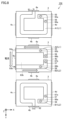
- FIG. 1 is a transparent perspective view of a coil component according to Embodiment 1.
- FIG. 1 is a transparent plan view of a coil component according to Embodiment 1.
- FIG. 3 is a plan view for explaining a wiring pattern of the coil component according to the first embodiment.
- 1 is a circuit diagram of a filter circuit including a coil component according to Embodiment 1.
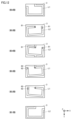
- FIG. 3 is a transparent side view showing a part of a coil component according to a second embodiment.
- FIG. 7 is a transparent side view showing a part of a coil component according to Embodiment 3;
- FIG. 7 is a transparent side view showing a part of a coil component according to a fourth embodiment.
- 7 is a plan view for explaining a wiring pattern of a coil component according to Modification 1.
- FIG. 1 is a transparent perspective view of a coil component according to Embodiment 1.
- FIG. 1 is a transparent plan view of a coil component according to Embodiment 1.
- FIG. 3 is
- FIG. 7 is a plan view for explaining a wiring pattern of a coil component according to a second modification. 7 is a transparent perspective view of a coil component according to modification example 3.
- FIG. FIG. 7 is a plan view of a coil component according to modification example 4.
- FIG. 7 is a plan view for explaining a wiring pattern of a coil component related to modification 5;
- FIG. 7 is a diagram showing an outline of a configuration when coil components related to modification 5 are stacked on top of each other.
- FIG. 7 is a diagram for explaining the principle of modification 5.
- FIG. FIG. 7 is a diagram for explaining the principle of modification 5.
- FIG. FIG. 7 is a diagram for explaining a comparative example regarding modification example 5.
- FIG. 7 is a diagram showing stress distribution in a cross section of a coil related to Modification Example 5.
- FIG. 1 is a transparent perspective view of a coil component 100 according to the first embodiment.
- FIG. 2 is a transparent plan view of the coil component 100 according to the first embodiment.
- FIG. 3 is a plan view for explaining the wiring pattern of the coil component 100 according to the first embodiment.
- the long side direction of the coil component 100 is the X direction
- the short side direction is the Y direction
- the height direction is the Z direction.
- the coil component 100 includes a coil L1 and a coil L2.
- the coil component 100 is composed of a ceramic layer laminate (insulator) 3 on which a substrate (ceramic green sheet) on which wiring patterns of a coil L1 (first coil) and a coil L2 (second coil) are formed is laminated. There is.
- the stacking direction of the ceramic layers is the Z direction, and the direction of the arrow indicates the upper layer direction.
- the laminate 3 has a pair of main surfaces facing each other and a plurality of side surfaces connecting the pair of main surfaces.
- first principal surface the top surface of the laminate 3
- second principal surface the bottom surface
- principal surface Sometimes referred to as the "principal surface.”
- a substrate on which the wiring pattern of the coil L1 is formed and a substrate on which the wiring pattern of the coil L2 is formed are stacked parallel to the main surface of the laminate 3 to form the coil L1 and the coil L2.
- FIGS. 1 to 3 illustrations of the respective substrates of the coil L1 and the coil L2 are omitted, and only the coil L1 and the coil L2 are shown.
- an electrode 4a (first electrode) is provided on one side (first side) of the two long sides of the laminate 3, and an electrode 4a (first electrode) is provided on the other side (second side). ) is provided with an electrode 4b (second electrode).
- an electrode 4c (third electrode) is provided on one side (third side)
- an electrode 4d (fourth electrode) is provided on the other side (fourth side). It is being As shown in FIGS. 1 and 2, the electrodes 4a to 4d are provided so as to extend from the side surface of the stacked body 3 to the first main surface and the second main surface.
- the coils L1 and L2 are arranged so that their winding axes are oriented in the normal direction to the main surface of the laminate 3, and have a rectangular shape.
- the coil L1 and the coil L2 are single-layer patterns, they are not closed patterns, but the shape of the opening is inferred from the pattern that produces the coil characteristics, other than the pattern for connecting to each electrode. is a rectangle.
- the openings of each of the coils L1 and L2 overlap each other and are magnetically coupled.
- FIG. 2 when the laminate 3 is viewed from the normal direction to the main surface, the opening pattern of the coil L1 and the opening pattern of the coil L2 overlap. Examples of rectangular openings include those with rounded coil wiring patterns and those with rounded corners.
- a coil L1 and a coil L2 having a wiring pattern as shown in FIG. 3 are arranged in an overlapping manner in the Z-axis direction. Thereby, the coil L1 and the coil L2 are arranged so that the openings thereof face in the normal direction to the main surface of the laminate 3.
- the wiring patterns of the coils L1 and L2 are formed, for example, by printing conductive paste (Ni paste) on a ceramic green sheet, which is a substrate, by a screen printing method.
- the laminate 3 is thus formed by laminating multiple layers of ceramic green sheets, which are substrates. Each layer constituting the laminate 3 is made of the same material. In this way, each layer of the laminate 3 is made of the same material, so after the lamination process of the laminate 3 is completed, during the batch firing process, the laminate 3 may peel or crack due to the difference in thermal expansion coefficient. This can prevent the possibility of this occurring.
- the coils L1 and L2 are each formed of one electrode layer (conductor). However, each of the coils L1 and L2 may be formed of a plurality of electrode layers (conductors). An example in which the coils L1 and L2 are formed of multiple electrode layers (conductors) will be described as a second embodiment.
- An end 91 (first end) of the coil L1 is connected to the electrode 4a.
- An end 93a (second end) of the coil L1 is connected to the electrode 4c.
- An end 92 (first end) of the coil L2 is connected to the electrode 4b.
- An end 93b (second end) of the coil L2 is connected to the electrode 4c. Therefore, the end 93a of the coil L1 and the end 93b of the coil L2 are connected by the electrode 4c.
- connection point between the coil L1 and the coil L2 exists at the electrode 4c.
- the distance from the connection point between coil L1 and coil L2 to electrode 4c is zero.
- the connection point between the coil L1 and the coil L2 will also be referred to as an "intermediate connection point.”
- the electrode 4c includes an intermediate connection point between the coil L1 and the coil L2.
- a current flowing from the electrode 4a (In) flows from the end 91 of the coil L1 to the end 93a, reaches the electrode 4c, and passes through the electrode 4c to the end 93b of the coil L2. flows into.
- the current flowing into the end 93b of the coil L2 flows into the end 92 of the coil L2 and reaches the electrode 4b (Out).
- the electrode 4a functions as an In terminal
- the electrode 4b functions as an Out terminal
- the electrode 4c functions as an intermediate connection terminal.
- the direction in which a magnetic field is generated when a current flows from the electrode 4a to the electrode 4c is the same as the direction in which a magnetic field is generated in the coil L2 when a current flows from the electrode 4c to the electrode 4b.
- FIG. 4 is a circuit diagram of filter circuit 1 including coil component 100 according to the first embodiment.
- the filter circuit 1 is, for example, an EMI removal filter, and is a third-order T-type LC filter circuit.
- a coil component 100 is used in this filter circuit 1.
- a third-order T-type LC filter circuit is used as the configuration of the filter circuit 1, but a fifth-order T-type LC filter circuit or a higher-order T-type LC filter circuit may be used.
- the coil component 100 having a similar configuration can also be applied to the above.
- the filter circuit 1 to which the coil component 100 is applied includes a capacitor C1 in addition to the coil component.
- the capacitor C1 is connected to the coil component 100.
- the capacitor C1 has one end connected to an electrode 4c that constitutes an intermediate connection point between the coil L1 and the coil L2, and the other end connected to the GND wiring.
- the capacitor C1 is constituted by, for example, a multilayer ceramic capacitor mainly composed of BaTiO3 (barium titanate).
- a multilayer ceramic capacitor mainly composed of other materials may be used.
- other types of capacitors such as an aluminum electrolytic capacitor may be used as the capacitor C1.
- the capacitor C1 has an inductor L3 as a parasitic inductance (equivalent series inductance (ESL)). As shown in FIG. 4, capacitor C1 is represented by a circuit configuration in which inductor L3 is connected in series with capacitor C1a. Note that the capacitor C1 may be configured so that the parasitic resistance (equivalent series resistance (ESR)) is equivalent to a circuit configuration in which the inductor L3 and the capacitor C1a are connected in series.
- ESR Equivalent series resistance
- the coil L1 and the coil L2 are magnetically coupled, producing a negative inductance component (-M) in series with the capacitor C1.
- This negative inductance component is shown as an inductor of -M in FIG.
- This negative inductance component can cancel the parasitic inductance (inductor L3) of the capacitor C1.
- the parasitic inductance component of the capacitor C1 can be made smaller in appearance.
- a filter circuit 1 composed of a capacitor C1, a coil L1, and a coil L2 cancels out the parasitic inductance of the capacitor C1 with a negative inductance component due to the mutual inductance between the coil L1 and the coil L2, thereby reducing the noise damping effect in the high frequency band. can be improved.
- the intermediate connection point between the coil L1 and the coil L2 exists at the electrode 4c.
- neither the coil L1 nor the coil L2 is provided with a wiring pattern extending from the intermediate connection point between the coil L1 and the coil L2 to the electrode 4c. Therefore, compared to the conventional configuration in which a wiring pattern is provided from the intermediate connection point between the coil L1 and the coil L2 to the electrode 4c, the distance of the wiring pattern does not change due to manufacturing variations, so the parasitic inductance It is possible to prevent variations in the size of the components. Since the coil component 100 according to the first embodiment is not provided with an extra wiring pattern that causes variations in the magnitude of the parasitic inductance component, there is no parasitic inductance component that depends on the wiring pattern.
- the coil component 100 it is possible to reduce the effort and cost required to maximize accuracy in order to suppress such variations. Therefore, according to the first embodiment, it is possible to provide a coil component that can prevent variations in the size of parasitic inductor components and a filter circuit including the coil component.
- the coil component 100 when used as a component for removing noise from a power line and current is caused to flow from the electrode 4a to the electrode 4b, the current flowing inside the laminate 3 passes through the electrode 4c outside the laminate 3. At this time, compared to the conventional pattern in which the current continues to flow inside the laminate 3, the electrode 4c exhibits a heat dissipation function, and the heat generated by the current is dissipated in the electrode 4c. Therefore, the heat dissipation effect of the coil component 100 can be improved.
- the coil component 100 according to the first embodiment has the effect that the procedure for testing continuity of the electrodes 4a to 4c and the coils L1 and L2 can be simplified.
- a conventional coil component in which a wiring pattern is provided from the intermediate connection point between coil L1 and coil L2 to electrode 4c, it is not possible to test the continuity between coil L1 and coil L2 by simply testing the continuity between electrode 4a and electrode 4b. It is not possible to confirm that there is no problem in conduction between the intermediate connection point and the electrode 4c. Since another wire is inserted between the intermediate connection point between the coil L1 and the coil L2 and the electrode 4c, it is necessary to inspect the disconnection state of this other wire and the connection state between this other wire and the electrode 4c. .
- the electrode 4c corresponding to the intermediate connection terminal functions as a conduction line that connects the coil L1 and the coil L2. Therefore, in the coil component 100, by testing the continuity between the electrodes 4a and 4b, it is possible to complete the continuity test of the electrodes 4a to 4c and the coils L1 and L2.
- the electrodes 4a and 4b function as mounting terminals connected in series to the power line. That is, the electrode 4a and the electrode 4b are constituted by mounting terminals.
- the size of the mounting terminals can be made larger compared to the case where the electrodes 4a and 4b are provided on the short sides of the laminate 3. can do.
- the heat generated in the mounting portion can be sufficiently dissipated by the width of the electrode.
- the end portion 91 of the coil L1 is disposed on the wide electrode 4a on the long side of the laminate 3, and the end 91 of the coil L1 is arranged on the wide electrode 4a on the long side of the laminate 3.
- the end portion 92 of the coil L2 is arranged at 4b, it is also possible to form a coil with a large opening by taking advantage of the distance from one end of the long side to the other end.
- Embodiment 1 discloses "a coil component in which the insulating layer constituting the first coil and the insulating layer constituting the second coil are composed of insulators made of the same material.”
- Embodiment 2 Next, a second embodiment will be described with reference to FIG.
- the coils L1 and L2 are formed of multiple electrode layers (conductors).
- the second embodiment has the same configuration as the first embodiment except that the coils L1 and L2 are formed of multiple electrode layers (conductors). Therefore, as in the first embodiment, the aperture pattern of the coil L1 and the aperture pattern of the coil L2 overlap when viewed from the normal direction of the aperture patterns.
- FIG. 5 is a transparent side view showing a part of the coil component 101 according to the second embodiment.
- FIG. 5(A) shows the vicinity of the electrode 4a of the coil component 101
- FIG. 5(B) shows the vicinity of the electrode 4b of the coil component 101
- FIG. 5(C) shows the vicinity of the electrode 4c of the coil component 101. It is.
- each of the coils L1 and L2 is formed of three electrode layers (conductors).
- FIG. 5 shows conductors 10a to 10c (first conductors) included in the ceramic green sheets in each layer of coil L1 and conductors 20a to 20c (second conductors) included in the ceramic green sheets in each layer of coil L2. has been done.
- the coil L1 is configured to include a plurality of conductors 10a to 10c laminated in the normal direction to the main surface of the laminate 3, and the coil L2 is configured to include It is configured to include a plurality of conductors 20a to 20c laminated in the normal direction to the main surface of the body 3.
- the materials of the ceramic green sheets of each layer are all the same. That is, in the second embodiment, like the first embodiment, each layer of the laminate 3 is made of the same material.
- each of the plurality of conductors 10a to 10c constituting the coil L1 has the same line shape (wiring pattern), and the plurality of conductors 20a constituting the coil L2 have the same line shape (wiring pattern).
- the line shape (wiring pattern) of each of the lines 20c to 20c is common.
- one end of the conductors 10a to 10c forming the coil L1 is connected to the electrode 4a. Therefore, the end 91 of the coil L1 is constituted by one end of the conductors 10a to 10c.
- one end of the conductors 20a to 20c forming the coil L2 is connected to the electrode 4b. Therefore, the end 92 of the coil L2 is constituted by one end of the conductors 20a-20c.
- end 93a of coil L1 is constituted by the other ends of conductors 10a-10c
- end 93b of coil L2 is constituted by the other ends of conductors 20a-20c.
- the conductors 10a to 10c are connected in parallel with the electrode 4a and the electrode 4c.
- Conductors 20a to 20c are connected in parallel with electrode 4b and electrode 4c.
- a parallel circuit made up of the conductors 10a to 10c and a parallel circuit made up of the conductors 20a to 20c are constructed.
- the ends 911-913 of the conductors 10a-10c are connected in parallel to the electrode 4a, and the ends 931a-933a of the conductors 10a-10c are connected in parallel to the electrode 4c.
- the ends 911 to 913 constitute the end 91 of the coil L1, and the ends 931a to 933a constitute the end 93a of the coil L1.
- Ends 921-923 of the conductors 20a-20c are connected in parallel to the electrode 4b, and ends 931b-933b of the conductors 20a-20c are connected in parallel to the electrode 4c.
- the ends 921 to 923 constitute the end 92 of the coil L2, and the ends 931b to 933b constitute the end 93b of the coil L2.
- the via conductors that connect the conductors 10a to 10c in parallel and the via conductors that connect the conductors 20a to 20c in parallel are not provided. That is, a via conductor connecting each of the conductors 10a to 10c is not provided between the end 91 of the coil L1 and the end 93a of the coil L1, and the end 92 of the coil L2 and the end 93a of the coil L2 are not provided. 93b, no via conductor is provided to connect each of the conductors 20a to 20c.
- the coil component 101 In the coil component 101 according to the second embodiment, current flows in parallel circuits in the conductors 10a to 10c and the conductors 20a to 20c laminated in multiple layers. Therefore, the coil component 101 can handle a large current.
- the electrodes 4a and 4c are used as wiring members for configuring the parallel circuit of the conductors 10a to 10c without using via conductors.
- the electrodes 4b and 4c are used as wiring members for configuring the parallel circuit of the conductors 20a to 20c without using via conductors. Therefore, according to the second embodiment, the cost for providing via conductors can be reduced. Furthermore, according to the second embodiment, it is possible to prevent peeling, cracking, etc. from occurring in the laminate 3 starting from the via conductor.
- the insulating layer when the conductors 10a to 10c are laminated and the insulating layer when the conductors 20a to 20c are laminated are made of an insulator made of the same material. . Therefore, in the second embodiment, "an insulating layer when a plurality of first conductors constituting a first coil are laminated and an insulating layer when a plurality of second conductors constituting a second coil are laminated are as follows. A coil component composed of an insulator made of the same material is disclosed.
- a three-layer conductor is used as an example in which the coils L1 and L2 are formed by conductors laminated in multiple layers.
- the number of conductor layers is not limited to three layers, and may be two layers or four or more layers.
- the conductors 10a to 10c stacked in multiple layers are connected at the electrodes 4a and 4c.
- it may be configured such that only some of the conductors 10a to 10c are connected to one of the electrodes 4a and 4c.
- any part of the conductors 10a to 10c may be connected using a via conductor.
- the conductors 20a to 20c may be configured such that only some of the conductors 20a to 20c are connected to one of the electrodes 4b and 4c.
- Embodiment 3 Next, a third embodiment will be described with reference to FIG.
- the third embodiment can be understood as a modification of the second embodiment.
- an example has been described in which via conductors are not used to configure parallel circuits of conductors 10a to 10c and conductors 20a to 20c.
- Embodiment 3 an example of configuring these parallel circuits using via conductors will be described.
- FIG. 6 is a transparent side view showing a part of the coil component 102 according to the third embodiment.
- FIG. 6(A) shows the vicinity of the electrode 4a of the coil component 102
- FIG. 6(B) shows the vicinity of the electrode 4b of the coil component 102
- FIG. 6(C) shows the vicinity of the electrode 4c of the coil component 102. It is.
- a pair of via conductors are connected near both ends of conductors 10a to 10c 51, and a pair of via conductors 52 connect the vicinity of both ends of the conductors 20a to 20c.
- a parallel circuit of the conductors 10a to 10c is formed in front of the electrodes 4a and 4c. Only one of the conductors 10a to 10c, for example, the conductor 10b, is connected to the electrode 4a and the electrode 4c.
- the via conductor 51 it is preferable to provide the via conductor 51 as close as possible to one end 91 and the other end 93a of the coil L1. Further, with such a configuration, it is possible to reduce locations where current density is high in each layer of the coil L1.
- a parallel circuit of the conductors 20a to 20c is formed in front of the electrodes 4a and 4c. Only one of the conductors 20a to 20c, for example, the conductor 20b, is connected to the electrode 4a and the electrode 4c.
- the via conductor 52 it is preferable to provide the via conductor 52 as close as possible to one end 92 and the other end 93b of the coil L2. Furthermore, with such a configuration, it is possible to reduce the number of locations where the current density is high in each layer of the coil L2.
- a parallel circuit is configured by the pair of via conductors 51 that connect the conductors 10a to 10c near both ends of the conductors 10a to 10c, and the conductors 10a to 10c.
- a parallel circuit is configured by a pair of via conductors 52 that connect the conductors 20a to 20c near both ends of the conductors 20a to 20c, and the conductors 20a to 20c.
- each of the conductors 10a to 10c is connected by a via conductor 51 near the end 93a of the coil L1, and each of the conductors 20a to 20c is connected to the via conductor 51 near the end 93b of the coil L2. 52.
- the vicinity of the end 93a of the coil L1 refers to a position as close as possible to the end 93a of the coil L1 without causing any problem in providing the via holes of the via conductor 52 in the conductors 20a to 20c.
- the conductors 10a to 10c there is a via conductor 52 in a portion that connects a wiring pattern that functions as a coil (a wiring pattern that forms an opening) and an electrode 4c.
- the side of the end 93b of the coil L2 includes the vicinity of the end 93b of the coil L2, and refers to a position closer to the end 93b than the midpoint between the ends 93b and 92 of the conductors 20a to 20c.
- the coil component 102 in the coil component 102 according to the third embodiment, among the conductors 10a to 10c composed of three layers, only the middle layer conductor 10b is connected to the electrode 4a. Other conductors 10a and 10c are connected to electrode 4a via conductor 10b and via conductor 51. If all of the conductors 10a to 10c are connected to the electrode 4a as in the second embodiment described above, there is no need to provide the via conductor 51.
- the conductor 10b is connected to the electrode 4a among the conductors 10a to 10c composed of three layers. Furthermore, for the same reason, the electrode 4b and the electrode 4c also have a similar configuration. Therefore, according to the coil component 102 according to the third embodiment, it is possible to prevent cracks from occurring in the laminate 3 during the manufacturing process of the laminate 3. Of course, if cracks are unlikely to occur during manufacturing, all of the conductors 10a to 10c are connected to the electrodes 4a and 4c, and similarly, all of the conductors 20a to 20c are connected to the electrodes 4b and 4c, and the vias are connected. A configuration in which the conductors 51 and 52 are not provided may also be adopted.
- the conductors connected to any of the electrodes 4a to 4c are the middle layer conductors 10b and 20b.
- the middle layer conductors 10b, 20b instead of the middle layer conductors 10b, 20b, the upper layer conductors 10a, 20a or the lower layer conductors 10c, 20c may be selected as the conductor to be connected to any of the electrodes 4a to 4c.
- two of the conductors 10a to 10c may be selected as the target, and similarly, two of the conductors 20a to 20c may be selected as the target.
- Embodiment 3 an example has been described in which a parallel circuit is configured by the conductors 10a to 10c and a pair of via conductors 51 that connect the conductors 10a to 10c near both ends of the conductors 10a to 10c. Similarly, an example has been described in which a parallel circuit is configured by a pair of via conductors 52 connecting the conductors 20a to 20c near both ends of the conductors 20a to 20c, and the conductors 20a to 20c.
- the configuration near the electrode 4a the configuration shown in FIG. 5(A) described as the second embodiment may be adopted.
- a parallel circuit is formed by the conductors 10a to 10c between the electrode 4a and the via conductor 51 near the end 93a of the conductors 10a to 10c.
- the structure near the electrode 4b may adopt the structure shown in FIG. 5(B) described as the second embodiment.
- a parallel circuit is formed by the conductors 20a to 20c between the electrode 4b and the via conductor 52 near the end 93b of the conductors 20a to 20c.
- Embodiment 4 Next, a fourth embodiment will be described with reference to FIG.
- the fourth embodiment can be understood as a modification of the third embodiment.
- the third embodiment an example has been described in which via conductors 51 and 52 are used to configure parallel circuits of conductors 10a to 10c and conductors 20a to 20c, respectively.
- a via conductor is further provided in each of the parallel circuits of the conductors 10a to 10c and the conductors 20a to 20c configured according to the third embodiment.
- FIG. 7 is a transparent side view showing a part of the coil component 103 according to the fourth embodiment.
- FIG. 7(A) shows the vicinity of the electrode 4a of the coil component 103
- FIG. 7(B) shows the vicinity of the electrode 4b of the coil component 103
- FIG. 7(C) shows the vicinity of the electrode 4c of the coil component 103. It is.
- the conductors 10a to 10c are A pair of via conductors 53 connecting the conductors 20a to 20c and a pair of via conductors 54 connecting the conductors 20a to 20c near both ends of the conductors 20a to 20c are further added.
- the fourth embodiment even if a connection failure occurs in one of the via conductors 51 and 53 provided near both ends of the conductors 10a to 10c, conduction can be maintained by the other. Similar effects can be achieved with the conductors 20a to 20c.
- additional via conductors are provided near both ends of the conductors 10a to 10c and the conductors 20a to 20c.
- additional via conductors may be provided only near one end of conductors 10a-10c and near one end of conductors 20a-20c.
- a via conductor 53 may be provided near the center of the conductors 10a to 10c, and a via conductor 54 may be similarly provided near the center of the conductors 20a to 20c.
- the positions where the via conductors 53 and 54 are provided are not limited to the vicinity of both ends of the conductors 10a to 10c and the conductors 20a to 20c.
- FIG. 8 is a plan view for explaining the wiring pattern of the coil component 104 according to the first modification.
- the coil L1 is constituted by first coil parts A1 and A2
- the coil L2 is constituted by second coil parts B1 and B2.
- the first coil part A1 is composed of a substrate (ceramic green sheet) on which the wiring pattern of the first coil part A1 is formed.
- the second coil portion B1 is constituted by a substrate on which the wiring pattern of the second coil portion B1 is formed.
- the first coil part A2 and the second coil part B2 are formed of a substrate on which the wiring pattern of the first coil part A2 and the wiring pattern of the second coil part B2 are formed.
- Coil L1 and coil L2 according to Modification Example 1 are composed of these three substrates (ceramic green sheets), in the Z-axis direction, from below, a substrate on which the wiring pattern of second coil part B1 is formed, and first coil part A2.
- a substrate having a wiring pattern formed thereon and a wiring pattern of the second coil part B2, and a substrate having a wiring pattern of the first coil part A1 formed thereon are laminated in this order.
- the coil L1 according to Modification 1 is composed of first coil parts A1 and A2.
- Coil L2 according to Modification 1 is comprised of second coil parts B1 and B2. Therefore, in Modification 1, the first coil part A2 that constitutes a part of the coil L1 and the second coil part B2 that constitutes a part of the coil L2 are arranged in the same layer.
- the first coil portion A1 and the first coil portion A2 are connected by via conductors 55 and 56.
- the via conductor 55 connects the connecting portion 65a of the first coil portion A1 and the connecting portion 65b of the first coil portion A2.
- the via conductor 56 connects the connecting portion 66a of the first coil portion A1 and the connecting portion 66b of the first coil portion A2.
- the second coil part B1 and the second coil part B2 are connected by via conductors 57 and 58.
- the via conductor 57 connects the connecting portion 67a of the second coil portion B1 and the connecting portion 67b of the second coil portion B2.
- the via conductor 58 connects the connecting portion 68a of the second coil portion B1 and the connecting portion 68b of the second coil portion B2.
- the end 91 of the coil L1 is connected to the electrode 4a.
- An end 93a of the coil L1 is connected to the electrode 4c.
- An end 92 of the coil L2 is connected to the electrode 4b.
- An end 93b of the coil L2 is connected to the electrode 4c.
- the electrode 4c includes an intermediate connection point between the coil L1 and the coil L2.
- the current flowing from the electrode 4a flows through the first coil portion A1 that constitutes the first layer of the coil L1, passes through the via conductors 55 and 56, and flows through the second layer of the coil L1. This leads to the first coil portion A2 that constitutes the.
- the current flowing into the first coil portion A2 flows leftward in the drawing and reaches the end portion 93a.
- the current that has reached the end portion 93a flows into the second coil portion B2, which constitutes the first layer of the coil L2, via the electrode 4c.
- the current flowing into the second coil portion B2 flows rightward in the drawing. Thereafter, the current passes through the via conductors 57 and 58 and reaches the second coil portion B1 that constitutes the second layer of the coil L2.
- the current flowing into the second coil portion B1 flows to the end portion 92 and reaches the electrode 4b.
- the end 93a of the coil L1 and the end 93b of the coil L2 are arranged at positions that do not overlap with each other.
- the electrode 4c including the intermediate connection point between the coil L1 and the coil L2 the end 93a of the coil L1 and the end 93b of the coil L2 are located apart in the y-axis direction.
- the end 93a of the coil L1 and the end 93a of the coil L2 are 93b are arranged in the electrode 4c so that the green sheets overlap each other with a small thickness between the laminated layers.
- the end 93a of the coil L1 and the end 93b of the coil L2 are arranged to overlap at the electrode 4c, the end 93a of the coil L1 and the end 93b of the coil L2 are Since the magnetic fields cancel each other out between them, the mutual inductance between the coil L1 and the coil L2 decreases.
- the end 93a of the coil L1 and the end 93b of the coil L2 are located at separate positions in the y-axis direction, and the end 93a of the coil L1 includes the end 93a of the coil L1.
- the first coil portion A2 and the second coil portion B2 including the end portion 93b of the coil L2 are located at separate positions on the same layer.
- the mutual inductance value can be adjusted to the required value.
- This method of preventing the wiring pattern of the coil L1 and the wiring pattern of the coil L2 in the region connected to the electrode 4c from overlapping when viewed from the stacking direction can also be applied to the first embodiment. For example, by expanding the electrode 4c in the Y-axis direction in FIG. 3, shifting the position of the end 93a in the +Y-axis direction, and shifting the position of the end 93b in the -Y-axis direction, a positional relationship that does not overlap when viewed from the stacking direction can be achieved. can do.
- the directions in which the ends 93a and 93b are shifted may be reversed.
- the coil L1 is composed of a plurality of first coil parts A1 and A2, and the coil L2 is composed of a plurality of second coil parts B1 and B2. Therefore, the degree of freedom in designing the coils can be increased compared to the case where the coils L1 and L2 are constructed from a single component.
- the performance of a coil is determined by the aperture, number of turns, etc.
- the degree of freedom of opening is limited, so it is necessary to adjust the performance of the coil by changing the number of turns.
- the number of turns of the coil can be finely adjusted in units of, for example, 0.5 rotations. It is also possible to form the coils L1 and L2 in separate layers for each 0.5 rotation, but by forming them in the same layer, the number of steps can be reduced and costs can be reduced.
- FIG. 9 is a plan view for explaining the wiring pattern of the coil component 105 according to the second modification.
- Modification 2 an example will be described in which the opening of the coil is expanded using the electrode 4d that is not used in each embodiment.
- the coil L1 is composed of first coil parts A11 and A12
- the coil L2 is composed of second coil parts B11 and B12.
- the first coil part A11 is composed of a substrate (ceramic green sheet) on which the wiring pattern of the first coil part A11 is formed.
- the second coil portion B11 is configured by a substrate on which a wiring pattern of the second coil portion B11 is formed.
- the first coil portion A12 and the second coil portion B12 are configured by a substrate on which a wiring pattern of the first coil portion A12 and a wiring pattern of the second coil portion B12 are formed.
- the coil L1 and the coil L2 according to Modification Example 2 are composed of these three substrates (ceramic green sheets), which in the Z-axis direction are, from below, a substrate on which the wiring pattern of the second coil part B11 is formed, and a first coil part A12. It is constructed by laminating in this order a substrate on which the wiring pattern of and the wiring pattern of the second coil portion B12 are formed, and a substrate on which the wiring pattern of the first coil portion A11 is formed.
- the coil L1 according to Modification 2 is composed of first coil parts A11 and A12.
- Coil L2 according to modification 2 is configured by second coil parts B11 and B12.
- the first coil portion A11 and the first coil portion A12 are connected by an electrode 4d that was not used in each embodiment.
- the second coil portion B11 and the second coil portion B12 are connected by via conductors 59 and 60.
- the via conductor 59 connects the connecting portion 69a of the second coil portion B11 and the connecting portion 69b of the second coil portion B12.
- the via conductor 60 connects the connecting portion 70a of the second coil portion B11 and the connecting portion 70b of the second coil portion B12.
- the end 91 of the coil L1 is connected to the electrode 4a.
- An end 93a of the coil L1 is connected to the electrode 4c.
- An end 92 of the coil L2 is connected to the electrode 4b.
- An end 93b of the coil L2 is connected to the electrode 4c.
- the electrode 4c includes an intermediate connection point between the coil L1 and the coil L2.
- the current flowing from the electrode 4a flows through the first coil portion A11 constituting the first layer of the coil L1, passes through the outer electrode 4d of the laminate 3, and flows into the coil L1.
- the current flowing into the first coil portion A12 flows into the second coil portion B12, which constitutes the first layer of the coil L2, via the electrode 4c.
- the current flowing into the second coil portion B12 passes through the via conductors 59 and 60 and reaches the second coil portion B11 that constitutes the second layer of the coil L2.
- the current flowing into the second coil portion B11 flows to the end portion 92 and reaches the electrode 4b.
- the opening is expanded by utilizing the electrode 4d (Non connect terminal) that does not contribute to either the current In terminal or Out terminal or the intermediate connection terminal of L1 and L2.
- the electrode 4d can be utilized as one of the means for adjusting the inductance component.
- FIG. 10 is a transparent perspective view for explaining the wiring pattern of the coil component 106 according to the third modification.
- Modification 3 is a straight line that passes through the center of the opening in the Z-axis direction through the coils L1 and L2 shown in FIG. It corresponds to the image rotated 90 degrees around .
- the end 91 of the coil L1 is connected to the electrode 4a installed on the short side.
- An end 93a of the coil L1 is connected to an electrode 4c installed on the long side.
- the end 92 of the coil L2 is connected to the electrode 4b installed on the short side.
- An end 93b of the coil L2 is connected to the electrode 4c. Therefore, in the third modification, the intermediate connection point between the coil L1 and the coil L2 is located at the electrode 4c on the side surface including the long side of the laminate 3.
- the electrode 4c is provided on the side surface on the long side of the laminate 3, by taking advantage of the length of the long side, the electrode 4c can be made smaller in size than the electrode 4b provided on the side surface on the short side of the laminate 3. It can be made larger.
- the electrode located at the intermediate connection point between the coil L1 and the coil L2 functions to radiate heat generated by the current.
- this function is performed by the electrode 4c on the shorter side of the laminate 3.
- this function is performed by the electrodes 4a on the long sides of the laminate 3. Since the size of the electrode 4a can be made larger than the electrode 4c, according to the third modification, the heat dissipation effect at the intermediate connection point between the coil L1 and the coil L2 can be further enhanced.
- the distance between the end 93a of the coil L1 and the end 93 of the coil L2 can be sufficiently increased by taking advantage of the length of the electrode 4a in the long side direction. Thereby, it is possible to prevent the inductances of the coils L1 and L2 from canceling each other out at the intermediate connection point. In particular, when Modification 3 is applied to Modifications 1 and 2, the effect is maximized.
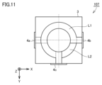
- FIG. 11 is a plan view for explaining the wiring pattern of the coil component 107 according to the fourth modification.
- the lengths of the sides on which the electrodes 4a, 4b, and 4c exist are equal, and the shape is square when viewed from the stacking direction.
- the coils L1 and L2 are configured in a circular shape. By making the coil circular, there are no places where the current density is locally high, so even when a large current is passed, local heat generation and associated failures are less likely to occur. Similar effects can be expected by forming a circular or oval shape on a rectangular chip as in the examples up to Modification Example 3.
- FIG. 12 is a plan view for explaining the wiring pattern of the coil component 108 according to the fifth modification.
- FIG. 13 is a diagram schematically showing a configuration when coil components 108 according to modification 5 are stacked on top of each other.
- the coil component 108 according to Modification 5 is configured by stacking six substrates on which the wiring pattern of the coil L1 or the coil L2 is formed.
- FIG. 12 shows wiring patterns formed on each of the first to sixth layer substrates. The first layer substrate is located at the bottom layer, and the sixth layer substrate is located at the top layer. In FIGS. 12 and 13, illustration of the electrodes 4a and 4c is omitted.
- the coils L1 and L2 shown in FIG. 12 have a rectangular shape like the coils L1 and L2 shown in FIG. 3.
- Coils L1 and L2 related to modification 5 are examples of a first conductor, a second conductor, and a third conductor that are laminated in the normal direction to the main surface. Each of the first conductor, second conductor, and third conductor has a rectangular shape.
- the coil L2 provided on the first layer substrate and the coil 1 provided on the sixth layer substrate are larger than the coils L1 and L2 provided on each of the second to fifth layers.
- the coils L1 and L2 provided in each of the second to fifth layers rotate about the center of the opening of the coil L2 provided in the first layer substrate, with reference to the coil L2 provided in the first layer substrate.
- the fourth layer coil L2 and the fifth layer coil L2 are connected by via conductors 81, 81.
- the second layer coil L1 and the third layer coil L1 are connected by via conductors 88 and 82.
- the coils L1 and L2 of each layer are stacked in the main surface direction (Z-axis direction).
- the coils L1 and L2 of the second to fifth layers are arranged inside the outer peripheral edge of the coil L1 of the first layer and the coil L2 of the second layer.
- each side of the coils L1 and L2 in each layer constitutes an outer peripheral edge and an inner peripheral edge of the wiring pattern of the coils L1 and L2 in each layer.
- each side of the coils L1 and L2 in each layer may be referred to as an edge.
- FIG. 13 shows L1 and L2 superimposed in the main surface direction (Z-axis direction) together with a schematic diagram.
- the coil component 108 when the laminate 3 is viewed from the normal direction to the pair of principal surfaces, the corresponding sides of each of the first conductor, second conductor, and third conductor constituting L1 and L2 are intersect. Further, the size of the first conductor (L2 of the first layer, L1 of the sixth layer) is larger than the size of the second conductor and the third conductor (L1, L2 of the second to fifth layers). Further, the second conductor and the third conductor (L1, L2 of the second to fifth layers) are arranged inside the outer edge of the first conductor (L2 of the first layer, L1 of the sixth layer). .
- each of the coil parts A21 to A23 shows a simplified wiring pattern of either L1 or L2 of the coil component 108.
- the sides (edges) of each of the coil portions A21 to A23 intersect.
- the coil portions A22 and A23 are included within the range of the outer peripheral edge of the coil portion A21.
- the symbol IP indicates the intersection of any two sides of the coil portions A21 to A23.
- the fifth modification there is a location where the sides of two of the coil parts A21 to A23 intersect.
- the sides of the coil portions A21 to A23 do not intersect at one location.
- the six layers do not intersect at one location, and the overlap of edges is limited to a maximum of four layers.
- stress concentration points can be distributed to various locations without concentrating stress on one side of the coil portion. As a result, it is possible to prevent cracks and the like from occurring in the coil component 108.
- FIGS. 14 and 15 are diagrams for explaining the principle of the fifth modification.
- FIG. 14(A) shows an example in which the coil parts A21 and A22 are stacked so that the wiring patterns of the coil parts A21 and A22 completely overlap.
- FIG. 14(B) shows an example in which the coil parts A21 and A22 are stacked such that the side of the coil part A21 and the side of the coil part A22 intersect at an appropriate angle.
- FIG. 14(C) shows an example in which the angle at which the side of the coil portion A21 and the side of the coil portion A22 intersect is larger than the configuration shown in FIG. 14(B).
- the sides of the coil part A21 and the sides of the coil part A22 are connected to each other to the extent that a plurality of gaps G1 appear between the sides of the coil part A21 and the sides of the coil part A22.
- the amount of deviation between In other words, in the configuration shown in FIG. 14C, the amount of deviation between the side of the coil portion A21 and the side of the coil portion A22 is large to the extent that it exceeds the coil width W1.
- the number of intersection points IP of each side of the coil portions A21 and A22 is greater than in the configuration shown in FIG. 14(B). Therefore, it is desirable that the amount of angular deviation between the side of the coil portion A21 and the side of the coil portion A22 does not exceed the coil width W1. Note that the preferable amount of angle deviation between the side of the coil portion A21 and the side of the coil portion A22 differs depending on the coil width and coil length.
- FIG. 15 shows an example in which three coil portions A21 to A23 are overlapped. If the principle explained using FIG. 14 is directly applied to the three coil portions A21 to A23, the configuration shown in FIG. 15(A) will be obtained.
- the outer diameter of the coil portion A21 is made larger than the outer diameter of the coil portions A22 and A23. That is, in order to reduce the overlap of the edges of the wiring patterns of the coil portion, "a wiring pattern having a size different from the wiring pattern shown in FIG. 15(A)" is adopted. More specifically, the size and position of the coil portions are adjusted so that the coil portions A22 and A23 are included within the outer circumferential edge of the coil portion A21. As a result, there is no intersection IP where the edges of all layers overlap as shown in FIG. 15(A).
- the coil component 108 related to Modification 5 was devised based on the principle explained above.
- the coil part A22 constituting the coil component 108 has a configuration in which it is rotated by a predetermined angle about the center of the opening of the coil part A22 in the XY plane as a rotation axis.
- the coil portion A23 constituting the coil component 108 has a configuration in which the center of the opening of the coil portion A23 in the XY plane is rotated by a predetermined angle in a direction opposite to the rotation direction of the coil portion A22. Another method for preventing large stress from collecting in one place is to shift the rotational axis of the coil portion A22 and the rotational axis of the coil portion A23.
- FIG. 16 is a diagram for explaining a comparative example regarding Modification 5.
- the comparative example shown in FIG. 16 is more likely to have problems during manufacturing than the fifth modification.
- the coil portion A22 is slightly smaller than the coil portion A21, and the coil portions are stacked with their opening axes aligned. With this configuration, stress can be prevented from being concentrated on the entire edge of each side of the coil portions A21 and A22, compared to the configuration shown in FIG. 14(A).
- the sides of the coil part A21 and the sides of the coil part A22 may overlap.
- FIG. 16(B) shows an example where misalignment occurs in the Y-axis direction in the process of stacking each layer of the coil portion. Considering such a phenomenon that occurs during the manufacturing process, the configuration as in the comparative example is not preferable.
- the mainstream process for manufacturing coil components is to manufacture an aggregate of several hundred or more pieces at once, and then cut out a plurality of desired coil components from the product. Therefore, the stacking misalignment affects all the coil parts cut out from the assembly. Therefore, in consideration of such a construction method, it can be said that the configuration of the comparative example is less preferable.
- Modification Example 5 does not have the same problem as the Comparative Example. This is because even if stacking misalignment occurs when manufacturing Modified Example 5, the intersection point IP will only shift from its original position in the X-axis direction or Y-axis direction, and the intersection point IP itself will not cease to exist. be. Therefore, the modification 5 is more resistant to misalignment that may occur during manufacturing than the comparative example shown in FIG. 16.
- FIG. 17 is a diagram showing the stress distribution in the cross section of coils L1 and L2 according to modification 5.
- FIG. 17 shows the relationship between the distance from the center of the long side of the coils L1 and L2 and the angle between the overlapping coils.
- the angle at which the edges of the coils L1 and L2 intersect is set to an appropriate angle (for example, 2 degrees)
- the overlapping edge portions will be dispersed, and stress concentration will be alleviated.
- Such a configuration corresponds to, for example, the configuration shown in FIG. 14(B). Note that the greater the distance from the center of the long sides of the coils L1 and L2, the greater the amount of edge deviation.
- Such a configuration corresponds to, for example, the configuration shown in FIG. 14(C). Therefore, when the edges of coil L1 and L2 intersect, make sure that the outer edge of one coil does not get too close to the inner edge of the other coil (so that the edge does not shift close to the coil width W1). It is necessary to set the intersection angle between the edge of coil L1 and the edge of coil L2.
- the side of the coil part A21 and the side of A22 intersect, the side of the coil part A22 and the side of A23 intersect, and the side of the coil part A23 intersects.
- the coil portions A21 to A23 are stacked so that the sides of A21 and A21 intersect with each other. Furthermore, in the fifth modification, the size and position of the coil portions are adjusted so that the coil portions A22 and A23 fit within the edge range of the outer periphery of the coil portion A21.
- the size of coil part A21 is larger than that of coil parts A22 and A23, but from the viewpoint of alleviating stress concentration, the size of coil part A21 should be larger than that of coil parts A22 and A3. You can also make it smaller. That is, when the laminate 3 is viewed from the normal direction to the main surface, the coil portion 21 is arranged in a range surrounded by the outer circumferential edge of the coil portion A22 and the outer circumferential edge of the coil portion A23. It's okay.
- modification 5 has been explained using three coil parts A21 to A23.
- the principle related to modification 5 may be applied to a coil component configured by stacking four or more coil parts.
- the shape of the coil portion may be basically a rectangular shape as shown in FIG. 12, or may be a rectangular shape with locally deformed portions.
- the shape may be such that a part of the rectangle has a concave portion or a convex portion.
- the configuration may be such that the corners of the rectangle are rounded.
- a part of the plurality of coil parts may include a circular or elliptical coil part.
- the first coil L1 and the second coil L2 were stacked with a part of the order changed, but if the shapes of the coil parts are the same, three layers of the first coil L1 are stacked adjacently. However, three layers of the second coils L2 may be stacked adjacently.
- the coil component described in Paragraph 1 is a coil component including a first coil and a second coil, an insulator on which the first coil and the second coil are arranged, and an insulator on which the first coil and the second coil are arranged.
- the insulator has a pair of main surfaces facing each other and a plurality of side surfaces connecting the pair of main surfaces, and the plurality of side surfaces include a first side surface, a second side surface, and a plurality of side surfaces.
- the plurality of electrodes include a first electrode provided on the first side surface, a second electrode provided on the second side surface, and a third electrode provided on the third side surface, the first coil and The second coil is arranged such that its winding axis is oriented in the normal direction to the pair of principal surfaces, and at least a portion of the openings of each of the first coil and the second coil overlap each other and are magnetically coupled, and the first coil
- the first end of the second coil is connected to the first electrode
- the first end of the second coil is connected to the second electrode
- the second end of the first coil and the second end of the second coil are connected to the first electrode. Connected by 3 electrodes.
- the first coil is configured to include a plurality of first conductors laminated in the normal direction to the pair of main surfaces.
- the second coil is configured to include a plurality of second conductors laminated in the normal direction to the pair of main surfaces.
- the plurality of first conductors are connected in parallel to the first electrode, and are connected in parallel to the third electrode, and the plurality of first conductors are connected in parallel to the third electrode.
- the two conductors are connected in parallel to the second electrode and in parallel to the third electrode.
- At least one of the plurality of first conductors and the plurality of second conductors is not provided with a via conductor that connects each conductor.
- At least one of the plurality of first conductors at least one of the first end and the second end of the first coil has a plurality of first conductors. It is not connected to the electrode of the first conductor, but is connected to the first conductor other than one first conductor by a via conductor.
- the first coil and the second coil are each formed of three layers of conductor, and at least one of the ends of the first coil and the second coil At each end, only the central conductor is connected to an electrode, and the conductors above and below the central conductor are connected to the central conductor via via conductors.
- each of the plurality of first conductors is connected by a first via conductor near the second end of the first coil, and each of the plurality of second conductors is , are connected by a second via conductor on the second end side of the second coil.
- the insulator is rectangular when viewed from the normal direction to the pair of main surfaces, and the first coil And the second coil is approximately rectangular.
- the insulator is square when viewed from the normal direction to the pair of main surfaces, and the first coil and the second coil is approximately circular.
- the first electrode and the second electrode are formed of mounting terminals.
- the first electrode and the second electrode are formed on opposing sides of the insulator.
- the first coil and the second coil include a first conductor, a second conductor, and a third conductor laminated in the normal direction to the pair of main surfaces.
- Each of the first conductor, second conductor, and third conductor has a rectangular shape, and when the insulator is viewed from the normal direction to the pair of main surfaces, the first conductor, the second conductor, and the third conductor have a rectangular shape.
- the filter circuit described in Item 19 includes the coil component described in any one of Items 1 to 18, and a capacitor connected to the third electrode of the coil component.
- 1 filter circuit 3 laminate, 4a, 4b, 4c, 4d electrode, 10a to 10c, 20a to 20c conductor, 51 to 60, 81, 82 via conductor, 65a, 65b, 66a, 66b, 67a, 67b, 68a, 68b, 69a, 69b, 70a, 70b, 81a, 82a Connection part, 91, 92, 93a, 93b, 921-923, 931a-933a, 931b-933b End part, 100-106 Coil parts, A1, A2, A1, A12, A21 to A23 Coil part, 1st coil part, B1, B2, B11, B12 2nd coil part, C1 capacitor, G1 gap, IP intersection, L1, L2 coil, W1 coil width.
Landscapes
- Engineering & Computer Science (AREA)
- Power Engineering (AREA)
- Microelectronics & Electronic Packaging (AREA)
- Coils Or Transformers For Communication (AREA)
Priority Applications (3)
| Application Number | Priority Date | Filing Date | Title |
|---|---|---|---|
| JP2024524248A JPWO2023233883A1 (https=) | 2022-06-01 | 2023-04-26 | |
| CN202390000344.5U CN223427310U (zh) | 2022-06-01 | 2023-04-26 | 线圈部件和包含该线圈部件的滤波电路 |
| TW112118489A TWI891007B (zh) | 2022-06-01 | 2023-05-18 | 線圈零件、及具備其之濾波器電路 |
Applications Claiming Priority (2)
| Application Number | Priority Date | Filing Date | Title |
|---|---|---|---|
| JP2022089815 | 2022-06-01 | ||
| JP2022-089815 | 2022-06-01 |
Publications (1)
| Publication Number | Publication Date |
|---|---|
| WO2023233883A1 true WO2023233883A1 (ja) | 2023-12-07 |
Family
ID=89026308
Family Applications (1)
| Application Number | Title | Priority Date | Filing Date |
|---|---|---|---|
| PCT/JP2023/016515 Ceased WO2023233883A1 (ja) | 2022-06-01 | 2023-04-26 | コイル部品、およびこれを含むフィルタ回路 |
Country Status (4)
| Country | Link |
|---|---|
| JP (1) | JPWO2023233883A1 (https=) |
| CN (1) | CN223427310U (https=) |
| TW (1) | TWI891007B (https=) |
| WO (1) | WO2023233883A1 (https=) |
Citations (4)
| Publication number | Priority date | Publication date | Assignee | Title |
|---|---|---|---|---|
| JPH08250309A (ja) * | 1995-10-26 | 1996-09-27 | Murata Mfg Co Ltd | 複合積層電子部品 |
| JP2012164828A (ja) * | 2011-02-07 | 2012-08-30 | Tdk Corp | チップ電子部品、チップ電子部品の実装構造、及びスイッチング電源回路 |
| WO2019187251A1 (ja) * | 2018-03-27 | 2019-10-03 | 株式会社村田製作所 | コイル部品および、これを含むフィルタ回路 |
| WO2021085002A1 (ja) * | 2019-10-30 | 2021-05-06 | 株式会社村田製作所 | コイル部品および、これを含むフィルタ回路 |
Family Cites Families (5)
| Publication number | Priority date | Publication date | Assignee | Title |
|---|---|---|---|---|
| JPH08139547A (ja) * | 1994-11-10 | 1996-05-31 | Taiyo Yuden Co Ltd | 積層emiフィルタ |
| JP4830674B2 (ja) * | 2005-07-04 | 2011-12-07 | Tdk株式会社 | サージ吸収素子 |
| TW200917563A (en) * | 2007-09-27 | 2009-04-16 | Murata Manufacturing Co | Laminated bandpass filter |
| CN113114150B (zh) * | 2015-12-24 | 2024-01-16 | 株式会社村田制作所 | 滤波器电路以及电容元件 |
| CN217588590U (zh) * | 2018-12-10 | 2022-10-14 | 株式会社村田制作所 | 线圈部件以及包含该线圈部件的滤波器电路 |
-
2023
- 2023-04-26 CN CN202390000344.5U patent/CN223427310U/zh active Active
- 2023-04-26 JP JP2024524248A patent/JPWO2023233883A1/ja active Pending
- 2023-04-26 WO PCT/JP2023/016515 patent/WO2023233883A1/ja not_active Ceased
- 2023-05-18 TW TW112118489A patent/TWI891007B/zh active
Patent Citations (4)
| Publication number | Priority date | Publication date | Assignee | Title |
|---|---|---|---|---|
| JPH08250309A (ja) * | 1995-10-26 | 1996-09-27 | Murata Mfg Co Ltd | 複合積層電子部品 |
| JP2012164828A (ja) * | 2011-02-07 | 2012-08-30 | Tdk Corp | チップ電子部品、チップ電子部品の実装構造、及びスイッチング電源回路 |
| WO2019187251A1 (ja) * | 2018-03-27 | 2019-10-03 | 株式会社村田製作所 | コイル部品および、これを含むフィルタ回路 |
| WO2021085002A1 (ja) * | 2019-10-30 | 2021-05-06 | 株式会社村田製作所 | コイル部品および、これを含むフィルタ回路 |
Also Published As
| Publication number | Publication date |
|---|---|
| TWI891007B (zh) | 2025-07-21 |
| JPWO2023233883A1 (https=) | 2023-12-07 |
| TW202403798A (zh) | 2024-01-16 |
| CN223427310U (zh) | 2025-10-10 |
Similar Documents
| Publication | Publication Date | Title |
|---|---|---|
| JP7238937B2 (ja) | コイル部品および、これを含むフィルタ回路 | |
| CN103219129B (zh) | 电子部件 | |
| CN101868838B (zh) | 层叠陶瓷电子元件 | |
| CN100458989C (zh) | 多端多层的陶瓷电子器件 | |
| JP4983874B2 (ja) | 積層コンデンサアレイの実装構造 | |
| JP6520801B2 (ja) | 電子部品 | |
| JP7318815B2 (ja) | フィルタ回路および、これを含む電源装置 | |
| CN100547706C (zh) | 三端电容器的安装结构 | |
| KR101408505B1 (ko) | 커먼 모드 필터 및 그 제조방법 | |
| CN107408931B (zh) | 电路基板、使用其的滤波器电路以及电容器元件 | |
| WO2021117392A1 (ja) | 多層基板、回路装置、およびフィルタ回路基板 | |
| WO2023233883A1 (ja) | コイル部品、およびこれを含むフィルタ回路 | |
| JP7553470B2 (ja) | 回路装置、およびフィルタ回路 | |
| CN220067840U (zh) | 多层构造体 | |
| CN222980246U (zh) | 线圈部件和包含该线圈部件的滤波电路 | |
| JP2012129773A (ja) | 電子部品の実装構造 | |
| US12537131B2 (en) | Electronic component | |
| JPH11340087A (ja) | 積層セラミックコンデンサ | |
| TWI848548B (zh) | 電子零件 | |
| JP2705412B2 (ja) | Lcフィルター | |
| TWI858536B (zh) | 電子零件 | |
| JP7760310B2 (ja) | 積層コイル部品 | |
| JP3252906B2 (ja) | 受動複合部品 | |
| WO2023181806A1 (ja) | 電子部品 | |
| JP2000349410A (ja) | 積層電子部品とその実装構造と製造方法 |
Legal Events
| Date | Code | Title | Description |
|---|---|---|---|
| 121 | Ep: the epo has been informed by wipo that ep was designated in this application |
Ref document number: 23815644 Country of ref document: EP Kind code of ref document: A1 |
|
| ENP | Entry into the national phase |
Ref document number: 2024524248 Country of ref document: JP Kind code of ref document: A |
|
| WWE | Wipo information: entry into national phase |
Ref document number: 202390000344.5 Country of ref document: CN |
|
| NENP | Non-entry into the national phase |
Ref country code: DE |
|
| 122 | Ep: pct application non-entry in european phase |
Ref document number: 23815644 Country of ref document: EP Kind code of ref document: A1 |
|
| WWP | Wipo information: published in national office |
Ref document number: 202390000344.5 Country of ref document: CN |