WO2023233459A1 - 接続構造 - Google Patents
接続構造 Download PDFInfo
- Publication number
- WO2023233459A1 WO2023233459A1 PCT/JP2022/021909 JP2022021909W WO2023233459A1 WO 2023233459 A1 WO2023233459 A1 WO 2023233459A1 JP 2022021909 W JP2022021909 W JP 2022021909W WO 2023233459 A1 WO2023233459 A1 WO 2023233459A1
- Authority
- WO
- WIPO (PCT)
- Prior art keywords
- tip
- insulated wires
- adhesive
- connection structure
- center conductor
- Prior art date
- Legal status (The legal status is an assumption and is not a legal conclusion. Google has not performed a legal analysis and makes no representation as to the accuracy of the status listed.)
- Ceased
Links
Images






Classifications
-
- H—ELECTRICITY
- H01—ELECTRIC ELEMENTS
- H01B—CABLES; CONDUCTORS; INSULATORS; SELECTION OF MATERIALS FOR THEIR CONDUCTIVE, INSULATING OR DIELECTRIC PROPERTIES
- H01B7/00—Insulated conductors or cables characterised by their form
- H01B7/17—Protection against damage caused by external factors, e.g. sheaths or armouring
- H01B7/28—Protection against damage caused by moisture, corrosion, chemical attack or weather
- H01B7/282—Preventing penetration of fluid, e.g. water or humidity, into conductor or cable
-
- H—ELECTRICITY
- H01—ELECTRIC ELEMENTS
- H01B—CABLES; CONDUCTORS; INSULATORS; SELECTION OF MATERIALS FOR THEIR CONDUCTIVE, INSULATING OR DIELECTRIC PROPERTIES
- H01B7/00—Insulated conductors or cables characterised by their form
- H01B7/02—Disposition of insulation
-
- H—ELECTRICITY
- H01—ELECTRIC ELEMENTS
- H01R—ELECTRICALLY-CONDUCTIVE CONNECTIONS; STRUCTURAL ASSOCIATIONS OF A PLURALITY OF MUTUALLY-INSULATED ELECTRICAL CONNECTING ELEMENTS; COUPLING DEVICES; CURRENT COLLECTORS
- H01R12/00—Structural associations of a plurality of mutually-insulated electrical connecting elements, specially adapted for printed circuits, e.g. printed circuit boards [PCB], flat or ribbon cables, or like generally planar structures, e.g. terminal strips, terminal blocks; Coupling devices specially adapted for printed circuits, flat or ribbon cables, or like generally planar structures; Terminals specially adapted for contact with, or insertion into, printed circuits, flat or ribbon cables, or like generally planar structures
- H01R12/50—Fixed connections
- H01R12/51—Fixed connections for rigid printed circuits or like structures
- H01R12/53—Fixed connections for rigid printed circuits or like structures connecting to cables except for flat or ribbon cables
-
- H—ELECTRICITY
- H01—ELECTRIC ELEMENTS
- H01R—ELECTRICALLY-CONDUCTIVE CONNECTIONS; STRUCTURAL ASSOCIATIONS OF A PLURALITY OF MUTUALLY-INSULATED ELECTRICAL CONNECTING ELEMENTS; COUPLING DEVICES; CURRENT COLLECTORS
- H01R4/00—Electrically-conductive connections between two or more conductive members in direct contact, i.e. touching one another; Means for effecting or maintaining such contact; Electrically-conductive connections having two or more spaced connecting locations for conductors and using contact members penetrating insulation
- H01R4/02—Soldered or welded connections
-
- H—ELECTRICITY
- H01—ELECTRIC ELEMENTS
- H01R—ELECTRICALLY-CONDUCTIVE CONNECTIONS; STRUCTURAL ASSOCIATIONS OF A PLURALITY OF MUTUALLY-INSULATED ELECTRICAL CONNECTING ELEMENTS; COUPLING DEVICES; CURRENT COLLECTORS
- H01R9/00—Structural associations of a plurality of mutually-insulated electrical connecting elements, e.g. terminal strips or terminal blocks; Terminals or binding posts mounted upon a base or in a case; Bases therefor
- H01R9/03—Connectors arranged to contact a plurality of the conductors of a multiconductor cable, e.g. tapping connections
- H01R9/05—Connectors arranged to contact a plurality of the conductors of a multiconductor cable, e.g. tapping connections for coaxial cables
-
- H—ELECTRICITY
- H05—ELECTRIC TECHNIQUES NOT OTHERWISE PROVIDED FOR
- H05K—PRINTED CIRCUITS; CASINGS OR CONSTRUCTIONAL DETAILS OF ELECTRIC APPARATUS; MANUFACTURE OF ASSEMBLAGES OF ELECTRICAL COMPONENTS
- H05K1/00—Printed circuits
- H05K1/18—Printed circuits structurally associated with non-printed electric components
-
- H—ELECTRICITY
- H05—ELECTRIC TECHNIQUES NOT OTHERWISE PROVIDED FOR
- H05K—PRINTED CIRCUITS; CASINGS OR CONSTRUCTIONAL DETAILS OF ELECTRIC APPARATUS; MANUFACTURE OF ASSEMBLAGES OF ELECTRICAL COMPONENTS
- H05K3/00—Apparatus or processes for manufacturing printed circuits
- H05K3/30—Assembling printed circuits with electric components, e.g. with resistors
- H05K3/32—Assembling printed circuits with electric components, e.g. with resistors electrically connecting electric components or wires to printed circuits
- H05K3/34—Assembling printed circuits with electric components, e.g. with resistors electrically connecting electric components or wires to printed circuits by soldering
Definitions
- the present disclosure relates to a connection structure.
- connection structure is described in Japanese Unexamined Patent Publication No. 2015-201280 (Patent Document 1).
- the connection structure described in Patent Document 1 includes a plurality of insulated wires, a printed wiring board, and a positioning sheet.
- each of the plurality of insulated wires the conductor is exposed from the insulating layer at the tip in the axial direction.
- the printed wiring board has a plurality of connected parts arranged in a row. The tip end of each of the plurality of insulated wires is soldered to each of the plurality of connected parts.
- the positioning sheet has an adhesive layer and a base film. The adhesive layer is bonded to the tips of the plurality of insulated wires. The base film is placed on the adhesive layer. The longitudinal direction of the positioning sheet is along the direction in which the plurality of connected parts are lined up (the direction in which the conductors of the plurality of insulated wires are lined up).
- connection structure described in Patent Document 1 is manufactured by the following method. First, a positioning step is performed. A jig is used in the positioning process. A plurality of positioning grooves are formed on the surface of the jig. The pitch between two adjacent ones of the plurality of positioning grooves is equal to the pitch between two adjacent ones of the plurality of connected parts. The tip end portion of each of the plurality of insulated wires is arranged in each of the plurality of positioning grooves.
- a positioning sheet is attached to the conductor.
- the adhesive layer is bonded to the tips of the plurality of insulated wires.
- the tips of each of the plurality of insulated wires are placed on each of the plurality of connected parts, and the adhesive layers at both longitudinal ends of the positioning sheet are bonded to the printed wiring board. .
- the tips of each of the plurality of insulated wires are soldered to each of the plurality of connected parts.
- the connection structure of the present disclosure includes a plurality of insulated wires, a base material, a plurality of connected parts arranged on the base material, and a sealing member.
- Each of the plurality of insulated wires has a center conductor and an insulating layer covering the circumferential surface of the center conductor. A central conductor is exposed from the insulating layer at the axial end of each of the plurality of insulated wires.
- the plurality of connected parts are arranged in a row.
- the tip end of each of the plurality of insulated wires is soldered to each of the plurality of connected parts.
- the sealing member is arranged on the base material so as to cover the tips of the plurality of insulated wires and the plurality of connected parts.
- FIG. 1 is a plan view of the connection structure 100.
- FIG. 2 is a sectional view taken along line II-II in FIG.
- FIG. 3 is a sectional view taken along line III-III in FIG.
- FIG. 4 is a sectional view taken along IV-IV in FIG.
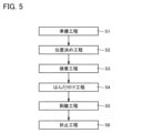
- FIG. 5 is a manufacturing process diagram of the connection structure 100.
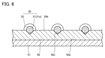
- FIG. 6 is a cross-sectional view illustrating the positioning step S2.
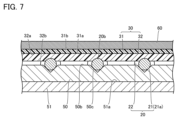
- FIG. 7 is a cross-sectional view illustrating the bonding step S3.
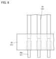
- FIG. 8 is a plan view illustrating the bonding step S3.
- FIG. 9A is a first cross-sectional view illustrating the soldering process S4.
- FIG. 9B is a second sectional view illustrating the soldering step S4.
- FIG. 9A is a first cross-sectional view illustrating the soldering process S4.
- FIG. 9B is a second sectional view illustrating the soldering step S4.
- FIG. 9A is a first cross-
- FIG. 9C is a plan view illustrating the soldering process S4.
- FIG. 10 is a cross-sectional view illustrating the peeling step S5.
- FIG. 11 is a side view of the insulated wire 20 used in the connection structure 100 according to the first modification.
- FIG. 12 is a cross-sectional view taken along line XII-XII in FIG.
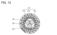
- FIG. 13 is a sectional view taken along line XIII-XIII in FIG. 11.
- FIG. 14 is a cross-sectional view of an insulated wire 20 used in a connection structure 100 according to a second modification.
- FIG. 15 is a cross-sectional view of a connection structure 100 according to a second modification.
- FIG. 16 is a plan view illustrating the soldering step S4 in the method for manufacturing the connection structure 100 according to the third modification.
- connection structure described in Patent Document 1 there is a space between two adjacent tips of the plurality of insulated wires. Therefore, in the connection structure described in Patent Document 1, there is room for improvement in the reliability of the connection portion between the tip end portion of each of the plurality of insulated wires and each of the plurality of connected portions.
- the present disclosure has been made in view of the problems of the prior art as described above. More specifically, the present disclosure provides a connection structure that can improve the reliability of the connection between the tip of each of a plurality of insulated wires and each of a plurality of connected parts.
- connection structure of the present disclosure it is possible to improve the reliability of the connection between the tip end of each of the plurality of insulated wires and each of the plurality of connected parts.
- a device includes a plurality of insulated wires according to an embodiment, a base material, a plurality of connected parts disposed on the base material, and a sealing member.
- Each of the plurality of insulated wires has a center conductor and an insulating layer covering the circumferential surface of the center conductor.
- a central conductor is exposed from the insulating layer at the axial end of each of the plurality of insulated wires.
- the plurality of connected parts are arranged in a row.
- the tip end of each of the plurality of insulated wires is soldered to each of the plurality of connected parts.
- the sealing member is arranged on the base material so as to cover the tips of the plurality of insulated wires and the plurality of connected parts.
- connection structure (1) it is possible to improve the reliability of the connection between the tip of each of the plurality of insulated wires and each of the plurality of connected parts.
- connection structure of (1) above may further include an adhesive.
- the adhesive may be bonded to the side surface of the tip of at least one of the plurality of insulated wires.
- connection structure (2) it is possible to prevent the positions of the tips of each of the plurality of insulated wires and the positions of each of the plurality of connected parts from becoming inconsistent with each other during soldering.
- the distance from the top of the tip to the tip of at least one of the plurality of insulated wires is less than 1/10 of the average diameter of the tip or 3 ⁇ m, whichever is smaller.
- the adhesive may also be applied to the circumferential surface of the larger tip.
- the distance from the top of the tip of at least one of the plurality of insulated wires to the tip is less than 1/3 of the average diameter of the tip or 10 ⁇ m, whichever is smaller.
- the adhesive may also be applied to the circumferential surface of the larger tip.
- the pitch between two adjacent parts of the plurality of connected parts may be 200 ⁇ m or less.
- the thickness of the sealing member on the tip portion may be 100 ⁇ m or less.
- connection structure (6) it is possible to reduce the height of the connecting portion between the tip end portion of each of the plurality of insulated wires and each of the plurality of connected portions.
- connection structure 100 The connection structure according to the embodiment is referred to as a connection structure 100.
- connection structure 100 (Configuration of connection structure 100) The configuration of the connection structure 100 will be explained below.
- FIG. 1 is a plan view of the connection structure 100.
- the connection structure 100 includes a printed wiring board 10, a plurality of insulated wires 20, and a sealing member 70. Although not shown, the plurality of insulated wires 20 are obtained by dividing one wire assembly.
- FIG. 2 is a sectional view taken along II-II in FIG. 1.
- the printed wiring board 10 includes a base material 11 and a plurality of wirings 12.
- the base material 11 has a first main surface 11a and a second main surface 11b.
- the first main surface 11a and the second main surface 11b are end faces of the base material 11 in the thickness direction.
- the base material 11 has a plate shape or a film shape, and is made of an electrically insulating material.
- the base material 11 is made of, for example, a resin material.
- the base material 11 is formed of, for example, glass epoxy.
- the base material 11 is formed of, for example, polyimide, polyethylene terephthalate, or the like.
- the constituent material of the base material 11 may contain fillers, additives, and the like.
- the wiring 12 is arranged on the first main surface 11a.
- the wiring 12 extends along the first direction DR1 in a plan view.
- Plane view refers to a view from a direction perpendicular to the first principal surface 11a.
- the plurality of wirings 12 are lined up at intervals in the second direction DR2. It is preferable that the plurality of wirings 12 are arranged at equal intervals in the second direction DR2.
- the second direction DR2 is a direction orthogonal to the first direction DR1.
- connection pad 12a The end of the wiring 12 in the first direction DR1 is a connection pad 12a.
- the connection pad 12a becomes a connected portion to which the tip portion 20a is connected.
- the connection pads 12a of the plurality of wirings 12 are arranged at intervals in the second direction DR2. It is preferable that the connection pads 12a of the plurality of wirings 12 are arranged at equal intervals.
- the pitch between two adjacent connection pads 12a of the plurality of wirings 12 is defined as a pitch P.
- the pitch P is the distance between the center of one connection pad 12a in the second direction DR2 and the center of another connection pad 12a adjacent to the one connection pad 12a in the second direction DR2. It is preferable that the pitch P is 200 ⁇ m or less.
- the surface of the connection pad 12a may be subjected to a plating process such as tin (Sn) plating process or gold (Au) plating process.
- the wiring 12 is made of a conductive material.
- the wiring 12 is made of copper (Cu) or a copper alloy, for example.
- the wiring 12 is formed, for example, by etching a conductive material placed on the base material 11 using a resist pattern as a mask.
- the method of forming the wiring 12 is not limited to this.
- the lower limit of the average thickness of the wiring 12 is preferably 3 ⁇ m, more preferably 5 ⁇ m, from the viewpoint of reducing the resistance of the wiring 12.
- the upper limit of the average thickness of the wiring 12 is preferably 100 ⁇ m, and more preferably 50 ⁇ m.
- the lower limit of the average width of the connection pads 12a is preferably 0.8 times the average diameter of the center conductor 21 from the viewpoint of ensuring connectivity with the center conductor 21, and is 1.0 times the average diameter of the center conductor 21. More preferably, it is twice as large.
- the upper limit of the average width of the connection pads 12a is preferably 5.0 times the average diameter of the center conductor 21, and 3.0 times the average diameter of the center conductor 21. It is more preferable that the diameter be 2.0 times the average diameter of the center conductor 21.
- FIG. 3 is a cross-sectional view taken along III-III in FIG. 1.
- the insulated wire 20 has a center conductor 21 and an insulating layer 22.
- the center conductor 21 is made of a conductive material.
- the center conductor 21 is a metal wire made of, for example, copper, copper alloy, aluminum (Al), aluminum alloy, or the like.
- the center conductor 21 is, for example, circular in cross-sectional view perpendicular to the axial direction.
- the “axial direction” is the direction in which the insulated wire 20 extends.
- the cross-sectional shape of the center conductor 21 is not limited to this.
- the center conductor 21 may be square or rectangular, for example.
- the lower limit of the average diameter of the center conductor 21 is preferably 10 ⁇ m, and more preferably 15 ⁇ m.
- the upper limit of the average diameter of the center conductor 21 is preferably 500 ⁇ m, more preferably 200 ⁇ m.
- the insulating layer 22 covers the peripheral surface of the center conductor 21.
- the insulating layer 22 is made of a flexible electrically insulating material.
- the insulating layer 22 is made of, for example, ethylene resin, a resin obtained by mixing ethylene resin with polyolefin, polyimide, polyamideimide, polyurethane, a silane crosslinked resin composition, a fluororesin, or the like.
- ethylene resin include polyethylene, ethylene vinyl acetate copolymer, ethylene ethyl acrylate copolymer, and the like.
- polyolefins include polypropylene, ethylene propylene rubber, styrene elastomer, and the like.
- Specific examples of the fluororesin include PTFE (polytetrafluoroethylene), PFA (perfluoroalkoxyalkane), FEP (perfluoroethylene propene copolymer), and the like.
- the insulating layer 22 can be formed, for example, by extruding the constituent material of the insulating layer 22 in a molten state onto the circumferential surface of the central conductor 21 and curing it, or by applying a paint in which the constituent material of the insulating layer 22 is dissolved in an organic solvent to the central conductor 21. It is arranged on the circumferential surface of the center conductor 21 by applying it onto the circumferential surface and then baking it.
- the average thickness of the insulating layer 22 is, for example, 3 ⁇ m or more and 1 mm or less.
- the insulated wire 20 has a tip 20a in the axial direction.
- the insulating layer 22 is removed from the circumferential surface of the center conductor 21. That is, the tip portion 20a is composed of the center conductor 21.
- the average length of the tip portion 20a in the axial direction is, for example, 0.2 mm or more and 3.0 mm or less.
- a primer layer may be interposed between the circumferential surface of the center conductor 21 and the insulating layer 22 in order to improve the adhesion between the circumferential surface of the center conductor 21 and the insulating layer 22. good.
- the primer layer is formed of, for example, a cured crosslinkable resin such as ethylene that does not contain metal hydroxide.
- FIG. 4 is a cross-sectional view taken along IV-IV in FIG. 1.
- the tip portion 20a of each of the plurality of insulated wires 20 is connected to each of the plurality of connection pads 12a by a connection portion 40.
- the connecting portion 40 is formed of a solder alloy such as a tin-silver-copper alloy, a tin-zinc (Zn)-bismuth (Bi) alloy, a tin-copper alloy, a tin-silver-indium (In)-bismuth alloy, etc.
- a solder alloy such as a tin-silver-copper alloy, a tin-zinc (Zn)-bismuth (Bi) alloy, a tin-copper alloy, a tin-silver-indium (In)-bismuth alloy, etc.
- the tip portion 20a has an upper end 20b.
- the distance between the tip portion 20a and the first main surface 11a in the third direction DR3 is greatest at the upper end 20b.
- the third direction DR3 is a direction orthogonal to the first direction DR1 and the second direction DR2.
- the third direction DR3 corresponds to the normal direction of the first main surface 11a.
- An adhesive 32 may be bonded to the side surface of at least one tip 20a of the plurality of insulated wires 20.
- the adhesive 32 may be bonded to the side surface of at least one tip 20a of the plurality of insulated wires 20 other than both ends in the second direction DR2.
- the sealing member 70 is arranged on the first main surface 11a so as to cover the tip portions 20a of the plurality of insulated wires 20 and the plurality of connection pads 12a.
- the sealing member 70 is made of, for example, an ultraviolet curable resin material. Let the thickness of the sealing member 70 on the tip portion 20a be the thickness T.
- the thickness T is preferably 100 ⁇ m or less.
- FIG. 5 is a manufacturing process diagram of the connection structure 100.
- the method for manufacturing the connection structure 100 includes a preparation step S1, a positioning step S2, an adhesion step S3, a soldering step S4, a peeling step S5, and a sealing step S6. have.
- the positioning step S2 is performed after the preparation step S1.
- the bonding step S3 is performed after the positioning step S2.
- the soldering process S4 is performed after the bonding process S3.
- the peeling process S5 is performed after the soldering process S4.
- the sealing step S6 is performed after the peeling step S5.
- a plurality of insulated wires 20 are prepared.
- a plurality of insulated wires 20 are divided from the assembled wire.
- the insulating layer 22 is removed at the tip 20a. Removal of the insulating layer 22 is performed by cutting the insulating layer 22 by irradiating a laser and peeling off the cut insulating layer 22.
- FIG. 6 is a cross-sectional view illustrating the positioning step S2. As shown in FIG. 6, the positioning step S2 is performed using a jig 50.
- the jig 50 is placed on a pedestal 51.
- the jig 50 has a first surface 50a and a second surface 50b.
- the first surface 50a is a surface facing the pedestal 51 side.
- the second surface 50b is the opposite surface to the first surface 50a.
- a plurality of positioning grooves 50c are formed on the second surface 50b.
- the positioning groove 50c extends linearly.
- the positioning groove 50c has a V-shape, for example, in a cross-sectional view orthogonal to the extending direction of the positioning groove 50c.
- the positioning groove 50c may be U-shaped in a cross-sectional view orthogonal to the extending direction of the positioning groove 50c.
- the plurality of positioning grooves 50c are arranged at intervals in a direction perpendicular to the direction in which the positioning grooves 50c extend.
- the pitch between two adjacent positioning grooves 50c is set to match the pitch P.
- the tips 20a of each of the plurality of insulated wires 20 are arranged in each of the plurality of positioning grooves 50c. Thereby, the pitch between two adjacent tips 20a of the plurality of insulated wires 20 is adjusted to match the pitch P.
- FIG. 7 is a cross-sectional view illustrating the bonding step S3. As shown in FIG. 7, in the bonding step S3, the pitch fixing film 30 is bonded to the tip portions 20a of the plurality of insulated wires 20 using the adhesive 32.
- the pitch fixing film 30 has a base material 31 and an adhesive 32.
- the base material 31 is, for example, a film-like member.
- the base material 31 has a first main surface 31a and a second main surface 31b.
- the first main surface 31a and the second main surface 31b are end faces of the base material 31 in the thickness direction.
- the first main surface 31a faces the base material 11 (printed wiring board 10) side.
- the lower limit of the average thickness of the base material 31 is preferably 5 ⁇ m, and more preferably 10 ⁇ m.
- the upper limit of the average thickness of the base material 31 is preferably 100 ⁇ m, and more preferably 50 ⁇ m.
- the base material 31 is made of, for example, super engineering plastic.
- super engineering plastics include polyimide, polyamideimide, polyetherimide, polyetheretherketone, polyphenylene sulfide, polyarylate, liquid crystal polymer, polysulfone, polyethersulfone, and fluororesins other than polytetrafluoroethylene. Can be mentioned.
- the adhesive 32 is arranged in a layered manner on the first main surface 31a.
- the adhesive 32 has a first surface 32a and a second surface 32b.
- the first surface 32a is a surface in contact with the base material 31 (first main surface 31a).
- the second surface 32b is the opposite surface to the first surface 32a.
- the average thickness of the adhesive 32 is smaller than the average thickness of the base material 31, for example. From the viewpoint of ensuring the strength of the adhesive 32, the lower limit of the average thickness of the adhesive 32 is preferably 5 ⁇ m, and more preferably 10 ⁇ m. From the viewpoint of reducing the height of the connection structure 100, the average thickness of the adhesive 32 is preferably 100 ⁇ m, and more preferably 50 ⁇ m.
- the adhesive 32 is, for example, a thermosetting adhesive whose main component is a thermosetting resin.
- the thermosetting resin is, for example, an epoxy resin containing a curing agent.
- epoxy resins include bisphenol A type epoxy resin, bisphenol F type epoxy resin, bisphenol S type epoxy resin, bisphenol AD type epoxy resin, copolymerization type epoxy resin of bisphenol A type and bisphenol F type, and naphthalene type epoxy resin. Examples include epoxy resin, novolac type epoxy resin, biphenyl type epoxy resin, dicyclopentadiene type epoxy resin, and the like.
- the adhesive 32 may contain at least one of these epoxy resins.
- the epoxy resin used for the adhesive 32 is preferably a combination of an epoxy resin with a molecular weight of 15,000 or more and an epoxy resin with a molecular weight of 2,000 or less.
- the molecular weight of the epoxy resin is the molecular weight in terms of polystyrene determined from gel permeation chromatography (GPC) developed with tetrahydrofuran (THF).
- a latent curing agent is a curing agent that has excellent storage stability at low temperatures and hardly causes a curing reaction at room temperature, but quickly performs a curing reaction when exposed to heat, light, or the like.
- Specific examples of latent curing agents include imidazole type, hydrazide type, boron trifluoride-amine complex, amine imide, polyamine type, tertiary amine, amine type such as alkyl urea type, dicyandiamide type, acid anhydride type, and Examples include phenolic compounds and modified products thereof.
- a curing agent for the epoxy resin one type or a mixture of two or more of these can be used.
- the curing agent contained in the epoxy resin is preferably an imidazole-based latent curing agent from the viewpoint of storage stability and rapid curing at low temperatures.
- imidazole-based latent curing agents include adducts of imidazole compounds with epoxy resins.
- Specific examples of imidazole compounds include imidazole, 2-methylimidazole, 2-ethylimidazole, 2-propylimidazole, 2-dodecylimidazole, 2-phenylimidazole, 2-phenyl-4-methylimidazole, 4-methylimidazole, etc. Can be mentioned.
- the imidazole-based latent curing agent is preferably microencapsulated from the viewpoint of long-term storage stability and fast curing.
- Microcapsules are made of polymer materials, metal materials, and inorganic materials.
- polymeric materials include polymeric materials containing polyurethane, polyester, etc. as a main component.
- metal material include nickel, copper, and the like.
- inorganic materials include calcium silicate and the like.
- the adhesive 32 may be a thermoplastic adhesive whose main component is a thermoplastic resin.
- thermoplastic resins include polyvinyl acetal such as polyvinyl butyral, phenoxy resin, acrylic resin, methacrylic resin, polyamide, polyacetal, polyphenylene sulfide, polyimide, polytetrafluoroethylene, polyether ether ketone, polyether sulfone, urethane, Examples include polyester, polyethylene, polypropylene, polystyrene, and the like.
- the thermoplastic resin is preferably phenoxy resin, polyamide, polyimide, or the like.
- the base material 31 and adhesive 32 have transparency. Thereby, the tip portion 20a can be visually recognized through the base material 31 and the adhesive 32, so that the manufacturability of the connection structure 100 is improved.
- the adhesive 32 is bonded to the side surface of the tip 20a. That is, the adhesive 32 is bonded to the portion of the circumferential surface of the tip 20a whose distance from the upper end 20b is greater than either 1/10 of the average diameter of the tip 20a (center conductor 21) or 3 ⁇ m, whichever is smaller. There is. To put this from another perspective, the distance between the upper end 20b and the second surface 32b is greater than either 1/10 of the average diameter of the tip portion 20a (center conductor 21) or 3 ⁇ m, whichever is smaller. ing.
- the lower limit of the thickness of the adhesive 32 between the upper end 20b and the base material 31 is preferably 1/10 of the average diameter of the center conductor 21. Preferably, it is more preferably 1/5 of the average diameter of the center conductor 21. From the viewpoint of the thickness of the adhesive 32 between the upper end 20b and the base material 31 and the reduction in the height of the connection structure 100, it is preferably 2/3 of the average diameter of the center conductor 21; More preferably, it is 1/2 of the diameter.
- the upper end 20b may be in contact with the base material 31. That is, the lower limit of the thickness of the adhesive 32 between the upper end 20b and the base material 31 may be 0.
- the adhesive strength between the tip 20a and the adhesive 32 is preferably lower than the bonding strength between the tip 20a and the connection pad 12a.
- FIG. 8 is a plan view illustrating the bonding step S3. As shown in FIG. 8, the tip portion 20a protrudes from the pitch fixing film 30 in plan view.
- the lower limit of the length of the tip portion 20a protruding from the pitch fixing film 30 is preferably 10 ⁇ m, more preferably 20 ⁇ m.
- the upper limit of the length of the tip portion 20a protruding from the pitch fixing film 30 is preferably 200 ⁇ m, more preferably 150 ⁇ m.
- the insulating layer 22 adjacent to the tip portion 20a overlaps the pitch fixing film 30 in plan view. That is, the insulating layer 22 adjacent to the tip portion 20a is bonded with the adhesive 32. Thereby, the boundary between the insulating layer 22 adjacent to the tip 20a and the tip 20a is protected by the adhesive 32.
- the lower limit of the width of the overlap between the insulating layer 22 and the pitch fixing film 30 adjacent to the tip portion 20a is preferably 10 ⁇ m, and preferably 20 ⁇ m.
- the upper limit of the width of the overlap between the insulating layer 22 and the pitch fixing film 30 adjacent to the tip portion 20a is preferably 500 ⁇ m, and preferably 300 ⁇ m.
- the pitch fixing film 30 is placed on the tip portions 20a of the plurality of insulated wires 20. At this time, the tips 20a of the plurality of insulated wires 20 are in contact with the adhesive 32. At this stage, the adhesive 32 has not been cured.
- the heating body 60 is brought into contact with the first principal surface 31a, and the heating body 60 presses the pitch fixing film 30 toward the tips 20a of the plurality of insulated wires 20.
- the side surfaces of the tip portions 20a of the plurality of insulated wires 20 are adhered to the adhesive 32, and the tip portions 20a of the plurality of insulated wires 20 are fixed to each other.
- the adhesive 32 is a thermosetting adhesive
- the adhesive 32 is turned into a B stage by heating with the heating element 60. After the bonding step S3 is performed, the jig 50 is removed.
- the pitch between two adjacent ones of the plurality of insulated wires 20 does not change even after the jig 50 is removed. It's tough.
- FIG. 9A is a first cross-sectional view illustrating the soldering step S4.
- FIG. 9B is a second sectional view illustrating the soldering step S4.
- a connection portion 40 is formed, and the tip end portion 20a of each of the plurality of insulated wires 20 is soldered to each of the plurality of connection pads 12a.
- the tip portions 20a of each of the plurality of insulated wires 20 are placed on each of the plurality of connection pads 12a with the plate-shaped solder 41 interposed therebetween.
- the heating temperature in the bonding step S3 may be a temperature at which the viscosity of the adhesive 32 is reduced so that a portion of the tip portion 20a is buried in the adhesive 32.
- the heating temperature in the bonding step S3 is, for example, 170°C or more and 350°C or less, and preferably 200°C or more and 320°C or less.
- the pressure applied in the bonding step S3 may be such that a portion of the tip portion 20a is buried in the softened adhesive 32.
- the pressure applied in the bonding step S3 is, for example, 0.1 MPa or more and 15 MPa or less, and preferably 0.5 MPa or more and 10 MPa or less.
- the tip 20a will be too buried in the adhesive 32 (that is, the tip 20a will be covered with the adhesive 32), and the tip will be damaged. It becomes impossible to connect the portion 20a and the connection pad 12a.
- the heating temperature in the bonding step S3 and the pressure applied in the bonding step S3 are too small, the tip 20a will not be buried in the adhesive 32 (that is, the adhesive 32 will not adhere to the side surface of the tip 20a), The force for maintaining the pitch between the tips 20a of two adjacent insulated wires 20 becomes weaker.
- the heating body 61 is brought into contact with the first main surface 31a, and the heating body 61 presses the pitch fixing film 30 toward the tip portions 20a of the plurality of insulated wires 20.
- the plate-shaped solder 41 is melted, and the tips 20a of each of the plurality of insulated wires 20 are soldered to each of the plurality of connection pads 12a.
- bar-shaped solder may be used instead of the plate-shaped solder 41.
- flux may be supplied to at least one of the surface of the plate-shaped solder 41 (rod-shaped solder), the surface of the tip portion 20a, and the surface of the connection pad 12a. This flux is, for example, an organic acid-based or rosin-based flux.
- soldering may be performed by bringing the heating body 61 into contact with the second main surface 11b to melt the plate-shaped solder 41 (rod-shaped solder).
- FIG. 9C is a plan view illustrating the soldering step S4.
- the pitch fixing film 30 at least partially overlaps the plurality of connection pads 12a in plan view.
- Both ends of the pitch fixing film 30 in the second direction DR2 are located at positions that protrude further outward than the outermost connection pad 12a in the second direction DR2.
- the lower limit of the amount of protrusion of both ends of the pitch fixing film 30 in the second direction DR2 is preferably twice the average diameter of the center conductor 21, and preferably 2.5 times the average diameter of the center conductor 21. More preferred.
- the upper limit of the amount of protrusion of both ends of the pitch fixing film 30 in the second direction DR2 is preferably 100 times the average diameter of the center conductor 21, and more preferably 50 times the average diameter of the center conductor 21. .
- both ends of the pitch fixing film 30 in the second direction DR2 may be bonded to the first main surface 11a, or may not be bonded to the first main surface 11a. Good too.
- FIG. 10 is a cross-sectional view illustrating the peeling step S5.
- the pitch fixing film 30 is peeled off from the tip portions 20a of the plurality of insulated wires 20 together with the adhesive 32.
- the adhesive 32 may not be completely peeled off. It may remain.
- the sealing member 70 covers the tip portions 20a of the plurality of insulated wires 20 and the plurality of connection pads 12a.
- the sealing member 70 is supplied onto the first main surface 11a so as to cover the tip portions 20a of the plurality of insulated wires 20 and the plurality of connection pads 12a.
- the sealing member 70 is uncured.
- the uncured sealing member 70 is irradiated with ultraviolet rays. As a result, the sealing member 70 is cured, and the tip portions 20a of the plurality of insulated wires 20 and the plurality of connection pads 12a are sealed with the sealing member 70.
- the connection structure 100 having the structure shown in FIGS. 1 to 4 is formed.
- connection structure 100 The effects of the connection structure 100 will be explained below.
- the sealing member 70 is disposed on the first main surface 11a so as to cover the tip portions 20a of the plurality of insulated wires 20 and the plurality of connection pads 12a, some of the plurality of insulated wires 20 A sealing member 70 is also filled between two adjacent tips 20a. Therefore, according to the connection structure 100, the reliability of the connection between the tip portion 20a and the connection pad 12a can be improved.
- connection structure 100 the adhesive 32 is bonded to the side surfaces of the tip portions 20a of the plurality of insulated wires 20 in the bonding step S3. Therefore, in the connection structure 100, the positions of the tips 20a of each of the plurality of insulated wires 20 are more firmly fixed with the adhesive 32. As a result, according to the connection structure 100, when soldering is performed, the position of the tip end 20a of each of the plurality of insulated wires 20 is difficult to shift from the position of each of the plurality of connection pads 12a, resulting in defective soldering. It is possible to prevent this from happening.
- the pitch fixing film 30 is peeled off from the tip portions 20a of the plurality of insulated wires 20.
- the soldering step S4 it is no longer necessary to fix the tips 20a of the plurality of insulated wires 20 to each other using the adhesive 32. Therefore, in the connection structure 100, since the pitch fixing film 30 is peeled off after the completion of the soldering process S4, each of the plurality of insulated wires 20 is connected when soldering is performed even without the pitch fixing film 30. The position of the tip end 20a is prevented from shifting from the position of each of the plurality of connection pads 12a.
- connection structure described in Patent Document 1 the adhesive layer at both ends of the positioning sheet in the longitudinal direction is attached to the printed wiring board for more reliable connection between the tip of the insulated wire and the connected part. It is glued. Therefore, in the connection structure described in Patent Document 1, it is not assumed that the positioning sheet is peeled off from the tip of the insulated wire.
- connection structure 100 since the pitch fixing film 30 is peeled off, it is possible to reduce the height by not having the pitch fixing film 30. Note that since the connection structure 100 includes the sealing member 70, the height of the portion where the tip portion 20a and the connection pad 12a are connected becomes large; however, if the thickness T is 100 ⁇ m or less, the height is low. Dorsal transformation is not inhibited.
- FIG. 11 is a side view of the insulated wire 20 used in the connection structure 100 according to the first modification.
- FIG. 12 is a cross-sectional view taken along line XII-XII in FIG.
- the center conductor 21 may be a twisted wire made by twisting a plurality of wires 21a.
- the average diameter of the tip portion 20a is determined based on a virtual circumscribed circle (indicated by a dotted line in FIG. 12) that circumscribes the plurality of wires 21a, and also determined based on the circumscribed circle. Based on the average diameter of the tip 20a, it is determined whether the adhesive 32 is adhered to the side surface of the tip 20a.
- the number of strands 21a constituting the center conductor 21 is not particularly limited, but is, for example, 2 or more and 20 or less.
- FIG. 13 is a cross-sectional view taken along line XIII-XIII in FIG. 11.
- the insulated wire 20 may further include a plurality of outer conductors 23 and a jacket 24. That is, the insulated wire 20 may be a coaxial wire.
- the outer conductor 23 is, for example, a metal wire made of copper or a copper alloy.
- the outer conductor 23 may be formed by performing silver plating, tin plating, etc. on the surface of this metal wire.
- the outer conductor 23 extends along the axial direction on the circumferential surface of the insulating layer 22.
- the outer conductor 23 may be spirally wound.
- the plurality of external conductors 23 cover the insulating layer 22 by being lined up along the circumferential surface of the insulating layer 22 .
- the cross-sectional shape of the external conductor 23 is, for example, circular, square, or rectangular.
- the lower limit of the average diameter of the outer conductor 23 is preferably 10 ⁇ m, more preferably 15 ⁇ m, from the viewpoint of suppressing breakage of the outer conductor 23.
- the upper limit of the average diameter of the outer conductor 23 is preferably 500 ⁇ m, more preferably 200 ⁇ m, from the viewpoint of preventing the outer diameter of the insulated wire 20 from becoming excessively large.
- the outer sheath 24 covers the plurality of external conductors 23.
- the outer cover 24 is made of a flexible electrically insulating material.
- the outer cover 24 is made of, for example, polyester resin such as polyethylene terephthalate.
- the outer cover 24 may be formed of the same material as the insulating layer 22.
- the insulated wire 20 has an adjacent portion 20c adjacent to the tip portion 20a in the axial direction. At the tip portion 20a, the center conductor 21 is exposed by removing the insulating layer 22, the plurality of outer conductors 23, and the outer sheath 24. In the adjacent portion 20c, the plurality of external conductors 23 are exposed by removing the outer cover 24. Note that the plurality of external conductors 23 are also removed from the tip end 20a side of the adjacent portion 20c.
- the plurality of external conductors 23 exposed in the adjacent portion 20c are electrically connected, for example, to a ground wire (not shown) arranged on the first main surface 11a by soldering or the like, and set to a ground potential. This functions as a shield to suppress electrical interference from other circuits.
- the average length of the adjacent portions 20c in the axial direction is, for example, 0.1 mm or more and 5 mm or less.
- the insulating layer 22 at the tip 20a is removed, the insulating layer 22 at the tip 20a and the adjacent portion 20c is removed.
- the outer sheath 24 as well as the plurality of outer conductors 23 at the tip 20a are removed.
- FIG. 14 is a cross-sectional view of an insulated wire 20 used in a connection structure 100 according to a second modification.
- the tip portion 20a may include a center conductor 21 and a solder layer 42 covering the center conductor 21.
- the average diameter of the solder layer 42 and the upper end of the solder layer 42 become the average diameter and the upper end 20b of the tip 20a, respectively, and it is determined based on these whether the adhesive 32 is bonded to the side surface of the tip 20a.
- the solder layer 42 is formed by supplying a molten solder alloy onto the circumferential surface of the center conductor 21 at the tip portion 20a after the insulating layer 22 is removed in the preparatory step S1.
- FIG. 15 is a cross-sectional view of a connection structure 100 according to Modification 2.
- FIG. 15 shows a cross section of the connection structure 100 according to Modification 2 at a position corresponding to FIG. 4 .
- the surface of the connection pad 12a may be covered with a solder layer 43.
- the solder layer 43 is formed, for example, by plating the surface of the connection pad 12a.
- the solder layer 42 and the solder layer 43 are bonded to each other to form the connection portion 40 by heating in the soldering step S4. Note that when the tip portion 20a has the solder layer 42 and the surface of the connection pad 12a is covered with the solder layer 43, the plate-shaped solder 41 (rod-shaped solder) is not used in the soldering process S4. , the flux is supplied to at least one of the surfaces of the solder layer 42 and the solder layer 43.
- FIG. 16 is a plan view illustrating the soldering step S4 in the method for manufacturing the connection structure 100 according to the third modification. As shown in FIG. 16, the pitch fixing film 30 does not need to overlap the plurality of connection pads 12a in plan view.
- the adhesive 32 does not need to be placed on the base material 31 in advance. That is, in the bonding step S3, the base material 31 may be bonded onto the adhesive 32 after the adhesive 32 is bonded to the tip portions 20a of the plurality of insulated wires 20.
Landscapes
- Engineering & Computer Science (AREA)
- Microelectronics & Electronic Packaging (AREA)
- Manufacturing & Machinery (AREA)
- Connections Effected By Soldering, Adhesion, Or Permanent Deformation (AREA)
Priority Applications (3)
| Application Number | Priority Date | Filing Date | Title |
|---|---|---|---|
| US18/868,699 US20250350046A1 (en) | 2022-05-30 | 2022-05-30 | Connection structure |
| JP2024524523A JPWO2023233459A1 (https=) | 2022-05-30 | 2022-05-30 | |
| PCT/JP2022/021909 WO2023233459A1 (ja) | 2022-05-30 | 2022-05-30 | 接続構造 |
Applications Claiming Priority (1)
| Application Number | Priority Date | Filing Date | Title |
|---|---|---|---|
| PCT/JP2022/021909 WO2023233459A1 (ja) | 2022-05-30 | 2022-05-30 | 接続構造 |
Publications (1)
| Publication Number | Publication Date |
|---|---|
| WO2023233459A1 true WO2023233459A1 (ja) | 2023-12-07 |
Family
ID=89025937
Family Applications (1)
| Application Number | Title | Priority Date | Filing Date |
|---|---|---|---|
| PCT/JP2022/021909 Ceased WO2023233459A1 (ja) | 2022-05-30 | 2022-05-30 | 接続構造 |
Country Status (3)
| Country | Link |
|---|---|
| US (1) | US20250350046A1 (https=) |
| JP (1) | JPWO2023233459A1 (https=) |
| WO (1) | WO2023233459A1 (https=) |
Citations (5)
| Publication number | Priority date | Publication date | Assignee | Title |
|---|---|---|---|---|
| JP2006164580A (ja) * | 2004-12-03 | 2006-06-22 | Hirose Electric Co Ltd | ケーブル付き電気コネクタ |
| JP2011171309A (ja) * | 2011-04-15 | 2011-09-01 | Sumitomo Electric Ind Ltd | 同軸ケーブルの接続構造およびその製造方法 |
| JP2012014934A (ja) * | 2010-06-30 | 2012-01-19 | Sumitomo Electric Ind Ltd | 同軸線ハーネス、そのモジュール、その電子機器およびその製造方法 |
| JP2014164842A (ja) * | 2013-02-22 | 2014-09-08 | Sumitomo Electric Ind Ltd | ケーブルハーネスおよびその加工方法 |
| JP2016092040A (ja) * | 2014-10-29 | 2016-05-23 | タツタ電線株式会社 | プリント基板、プリント基板の製造方法及び導電性部材の接合方法 |
-
2022
- 2022-05-30 JP JP2024524523A patent/JPWO2023233459A1/ja active Pending
- 2022-05-30 WO PCT/JP2022/021909 patent/WO2023233459A1/ja not_active Ceased
- 2022-05-30 US US18/868,699 patent/US20250350046A1/en active Pending
Patent Citations (5)
| Publication number | Priority date | Publication date | Assignee | Title |
|---|---|---|---|---|
| JP2006164580A (ja) * | 2004-12-03 | 2006-06-22 | Hirose Electric Co Ltd | ケーブル付き電気コネクタ |
| JP2012014934A (ja) * | 2010-06-30 | 2012-01-19 | Sumitomo Electric Ind Ltd | 同軸線ハーネス、そのモジュール、その電子機器およびその製造方法 |
| JP2011171309A (ja) * | 2011-04-15 | 2011-09-01 | Sumitomo Electric Ind Ltd | 同軸ケーブルの接続構造およびその製造方法 |
| JP2014164842A (ja) * | 2013-02-22 | 2014-09-08 | Sumitomo Electric Ind Ltd | ケーブルハーネスおよびその加工方法 |
| JP2016092040A (ja) * | 2014-10-29 | 2016-05-23 | タツタ電線株式会社 | プリント基板、プリント基板の製造方法及び導電性部材の接合方法 |
Also Published As
| Publication number | Publication date |
|---|---|
| JPWO2023233459A1 (https=) | 2023-12-07 |
| US20250350046A1 (en) | 2025-11-13 |
Similar Documents
| Publication | Publication Date | Title |
|---|---|---|
| US5804882A (en) | Semiconductor device having a semiconductor chip electrically connected to a wiring substrate | |
| US6034331A (en) | Connection sheet and electrode connection structure for electrically interconnecting electrodes facing each other, and method using the connection sheet | |
| TWI387412B (zh) | Electrical device, connection method and subsequent film | |
| US20110139500A1 (en) | Electrical connecting method and electrically connected connection structure | |
| KR100367955B1 (ko) | 솔더볼과 기판 사이의 결합이 강화된 반도체 장치 | |
| US20030201118A1 (en) | Production method of anisotropic conductive film and anisotropic conductive film produced by this method | |
| WO2023233459A1 (ja) | 接続構造 | |
| WO2023233458A1 (ja) | 接続構造及び接続構造の製造方法 | |
| JP7509013B2 (ja) | 電気的接続構造、並びに絶縁電線及びプリント配線板の接続体 | |
| JP2015201280A (ja) | 電気的接続方法、電気的接続構造、並びに絶縁電線及びプリント配線板の接続体 | |
| JP2002290028A (ja) | プリント配線基板の接続方法及び接続構造 | |
| KR100961589B1 (ko) | 접착재 릴 및 이를 이용한 회로 접속체의 제조 방법 | |
| JP7740060B2 (ja) | 接続体 | |
| JP7735719B2 (ja) | 電気的接続構造、並びに絶縁電線及びプリント配線板の接続体 | |
| KR101074161B1 (ko) | 절연 와이어 어셈블리 | |
| JP2008303067A (ja) | 接着材リール及びこれを用いた回路接続体の製造方法 | |
| JPS60140896A (ja) | 配線基板 | |
| KR19990029275A (ko) | 평면 디스플레이 장치 | |
| KR980013552A (ko) | 서로 마주보는 전극들을 상호접속하기 위한 접속시트 및 이 접속시트를 사용하는 전극 접속구조 및 접속방법 | |
| US5431863A (en) | Method of mounting semiconductor device | |
| JP4893175B2 (ja) | 回路板 | |
| JP2016184479A (ja) | ワイヤハーネス接続用フレキシブルフラットケーブル、ワイヤハーネス及びワイヤハーネス接続用フレキシブルフラットケーブルの製造方法 | |
| JP2006339163A (ja) | 電極の接続方法 | |
| JP2022544451A (ja) | 異方性導電接着フィルムの製造方法 | |
| JP4794397B2 (ja) | 配線基板の接続構造 |
Legal Events
| Date | Code | Title | Description |
|---|---|---|---|
| 121 | Ep: the epo has been informed by wipo that ep was designated in this application |
Ref document number: 22944749 Country of ref document: EP Kind code of ref document: A1 |
|
| WWE | Wipo information: entry into national phase |
Ref document number: 2024524523 Country of ref document: JP |
|
| WWE | Wipo information: entry into national phase |
Ref document number: 18868699 Country of ref document: US |
|
| NENP | Non-entry into the national phase |
Ref country code: DE |
|
| 122 | Ep: pct application non-entry in european phase |
Ref document number: 22944749 Country of ref document: EP Kind code of ref document: A1 |
|
| WWP | Wipo information: published in national office |
Ref document number: 18868699 Country of ref document: US |