WO2023223127A1 - 半導体装置、記憶装置及び電子機器 - Google Patents
半導体装置、記憶装置及び電子機器 Download PDFInfo
- Publication number
- WO2023223127A1 WO2023223127A1 PCT/IB2023/054529 IB2023054529W WO2023223127A1 WO 2023223127 A1 WO2023223127 A1 WO 2023223127A1 IB 2023054529 W IB2023054529 W IB 2023054529W WO 2023223127 A1 WO2023223127 A1 WO 2023223127A1
- Authority
- WO
- WIPO (PCT)
- Prior art keywords
- conductor
- insulator
- layer
- oxide semiconductor
- oxide
- Prior art date
- Legal status (The legal status is an assumption and is not a legal conclusion. Google has not performed a legal analysis and makes no representation as to the accuracy of the status listed.)
- Ceased
Links
Images

































Classifications
-
- H—ELECTRICITY
- H10—SEMICONDUCTOR DEVICES; ELECTRIC SOLID-STATE DEVICES NOT OTHERWISE PROVIDED FOR
- H10D—INORGANIC ELECTRIC SEMICONDUCTOR DEVICES
- H10D30/00—Field-effect transistors [FET]
- H10D30/60—Insulated-gate field-effect transistors [IGFET]
- H10D30/67—Thin-film transistors [TFT]
-
- H—ELECTRICITY
- H10—SEMICONDUCTOR DEVICES; ELECTRIC SOLID-STATE DEVICES NOT OTHERWISE PROVIDED FOR
- H10B—ELECTRONIC MEMORY DEVICES
- H10B12/00—Dynamic random access memory [DRAM] devices
- H10B12/50—Peripheral circuit region structures
-
- G—PHYSICS
- G11—INFORMATION STORAGE
- G11C—STATIC STORES
- G11C11/00—Digital stores characterised by the use of particular electric or magnetic storage elements; Storage elements therefor
- G11C11/21—Digital stores characterised by the use of particular electric or magnetic storage elements; Storage elements therefor using electric elements
- G11C11/34—Digital stores characterised by the use of particular electric or magnetic storage elements; Storage elements therefor using electric elements using semiconductor devices
- G11C11/40—Digital stores characterised by the use of particular electric or magnetic storage elements; Storage elements therefor using electric elements using semiconductor devices using transistors
- G11C11/401—Digital stores characterised by the use of particular electric or magnetic storage elements; Storage elements therefor using electric elements using semiconductor devices using transistors forming cells needing refreshing or charge regeneration, i.e. dynamic cells
- G11C11/403—Digital stores characterised by the use of particular electric or magnetic storage elements; Storage elements therefor using electric elements using semiconductor devices using transistors forming cells needing refreshing or charge regeneration, i.e. dynamic cells with charge regeneration common to a multiplicity of memory cells, i.e. external refresh
- G11C11/405—Digital stores characterised by the use of particular electric or magnetic storage elements; Storage elements therefor using electric elements using semiconductor devices using transistors forming cells needing refreshing or charge regeneration, i.e. dynamic cells with charge regeneration common to a multiplicity of memory cells, i.e. external refresh with three charge-transfer gates, e.g. MOS transistors, per cell
-
- G—PHYSICS
- G11—INFORMATION STORAGE
- G11C—STATIC STORES
- G11C5/00—Details of stores covered by group G11C11/00
- G11C5/06—Arrangements for interconnecting storage elements electrically, e.g. by wiring
- G11C5/063—Voltage and signal distribution in integrated semi-conductor memory access lines, e.g. word-line, bit-line, cross-over resistance, propagation delay
-
- H—ELECTRICITY
- H10—SEMICONDUCTOR DEVICES; ELECTRIC SOLID-STATE DEVICES NOT OTHERWISE PROVIDED FOR
- H10B—ELECTRONIC MEMORY DEVICES
- H10B12/00—Dynamic random access memory [DRAM] devices
-
- H—ELECTRICITY
- H10—SEMICONDUCTOR DEVICES; ELECTRIC SOLID-STATE DEVICES NOT OTHERWISE PROVIDED FOR
- H10B—ELECTRONIC MEMORY DEVICES
- H10B41/00—Electrically erasable-and-programmable ROM [EEPROM] devices comprising floating gates
- H10B41/70—Electrically erasable-and-programmable ROM [EEPROM] devices comprising floating gates the floating gate being an electrode shared by two or more components
-
- H—ELECTRICITY
- H10—SEMICONDUCTOR DEVICES; ELECTRIC SOLID-STATE DEVICES NOT OTHERWISE PROVIDED FOR
- H10B—ELECTRONIC MEMORY DEVICES
- H10B43/00—EEPROM devices comprising charge-trapping gate insulators
- H10B43/20—EEPROM devices comprising charge-trapping gate insulators characterised by three-dimensional [3D] arrangements, e.g. with cells on different height levels
- H10B43/23—EEPROM devices comprising charge-trapping gate insulators characterised by three-dimensional [3D] arrangements, e.g. with cells on different height levels with source and drain on different levels, e.g. with sloping channels
- H10B43/27—EEPROM devices comprising charge-trapping gate insulators characterised by three-dimensional [3D] arrangements, e.g. with cells on different height levels with source and drain on different levels, e.g. with sloping channels the channels comprising vertical portions, e.g. U-shaped channels
-
- H—ELECTRICITY
- H10—SEMICONDUCTOR DEVICES; ELECTRIC SOLID-STATE DEVICES NOT OTHERWISE PROVIDED FOR
- H10B—ELECTRONIC MEMORY DEVICES
- H10B99/00—Subject matter not provided for in other groups of this subclass
-
- H—ELECTRICITY
- H10—SEMICONDUCTOR DEVICES; ELECTRIC SOLID-STATE DEVICES NOT OTHERWISE PROVIDED FOR
- H10D—INORGANIC ELECTRIC SEMICONDUCTOR DEVICES
- H10D30/00—Field-effect transistors [FET]
- H10D30/60—Insulated-gate field-effect transistors [IGFET]
- H10D30/67—Thin-film transistors [TFT]
- H10D30/6729—Thin-film transistors [TFT] characterised by the electrodes
- H10D30/673—Thin-film transistors [TFT] characterised by the electrodes characterised by the shapes, relative sizes or dispositions of the gate electrodes
- H10D30/6733—Multi-gate TFTs
- H10D30/6734—Multi-gate TFTs having gate electrodes arranged on both top and bottom sides of the channel, e.g. dual-gate TFTs
-
- H—ELECTRICITY
- H10—SEMICONDUCTOR DEVICES; ELECTRIC SOLID-STATE DEVICES NOT OTHERWISE PROVIDED FOR
- H10D—INORGANIC ELECTRIC SEMICONDUCTOR DEVICES
- H10D30/00—Field-effect transistors [FET]
- H10D30/60—Insulated-gate field-effect transistors [IGFET]
- H10D30/67—Thin-film transistors [TFT]
- H10D30/674—Thin-film transistors [TFT] characterised by the active materials
- H10D30/6755—Oxide semiconductors, e.g. zinc oxide, copper aluminium oxide or cadmium stannate
-
- H—ELECTRICITY
- H10—SEMICONDUCTOR DEVICES; ELECTRIC SOLID-STATE DEVICES NOT OTHERWISE PROVIDED FOR
- H10D—INORGANIC ELECTRIC SEMICONDUCTOR DEVICES
- H10D84/00—Integrated devices formed in or on semiconductor substrates that comprise only semiconducting layers, e.g. on Si wafers or on GaAs-on-Si wafers
-
- H—ELECTRICITY
- H10—SEMICONDUCTOR DEVICES; ELECTRIC SOLID-STATE DEVICES NOT OTHERWISE PROVIDED FOR
- H10D—INORGANIC ELECTRIC SEMICONDUCTOR DEVICES
- H10D84/00—Integrated devices formed in or on semiconductor substrates that comprise only semiconducting layers, e.g. on Si wafers or on GaAs-on-Si wafers
- H10D84/01—Manufacture or treatment
- H10D84/0123—Integrating together multiple components covered by H10D12/00 or H10D30/00, e.g. integrating multiple IGBTs
- H10D84/0126—Integrating together multiple components covered by H10D12/00 or H10D30/00, e.g. integrating multiple IGBTs the components including insulated gates, e.g. IGFETs
-
- H—ELECTRICITY
- H10—SEMICONDUCTOR DEVICES; ELECTRIC SOLID-STATE DEVICES NOT OTHERWISE PROVIDED FOR
- H10D—INORGANIC ELECTRIC SEMICONDUCTOR DEVICES
- H10D84/00—Integrated devices formed in or on semiconductor substrates that comprise only semiconducting layers, e.g. on Si wafers or on GaAs-on-Si wafers
- H10D84/01—Manufacture or treatment
- H10D84/02—Manufacture or treatment characterised by using material-based technologies
- H10D84/03—Manufacture or treatment characterised by using material-based technologies using Group IV technology, e.g. silicon technology or silicon-carbide [SiC] technology
- H10D84/038—Manufacture or treatment characterised by using material-based technologies using Group IV technology, e.g. silicon technology or silicon-carbide [SiC] technology using silicon technology, e.g. SiGe
-
- H—ELECTRICITY
- H10—SEMICONDUCTOR DEVICES; ELECTRIC SOLID-STATE DEVICES NOT OTHERWISE PROVIDED FOR
- H10B—ELECTRONIC MEMORY DEVICES
- H10B12/00—Dynamic random access memory [DRAM] devices
- H10B12/01—Manufacture or treatment
- H10B12/09—Manufacture or treatment with simultaneous manufacture of the peripheral circuit region and memory cells
Definitions
- the second conductor is located on the top surface and side surfaces of the first oxide semiconductor, and in a region that does not overlap with the first oxide semiconductor.
- the third conductor is located on the top surface of the first oxide semiconductor.
- the fourth insulator is located between the second conductor and the third conductor in cross-sectional view and on the upper surface of the first oxide semiconductor, and the fourth conductor is located on the upper surface of the fourth insulator.
- the fifth conductor is located on the top surface of the first oxide semiconductor, and the fifth insulator is located between the third conductor and the fifth conductor in a cross-sectional view and on the top surface of the first oxide semiconductor.
- the sixth conductor is located on the upper surface of the fifth insulator.
- one embodiment of the present invention includes a first layer, a second layer, a first insulator, a second insulator, and a first conductor, and has a different configuration from the above (7). , a semiconductor device.
- each of the first layer and the second layer includes a first oxide semiconductor, a second conductor, a third conductor, a fourth conductor, a fifth conductor, and a sixth conductor.
- a seventh conductor, an eighth conductor, a ninth conductor, a tenth conductor, a fourth insulator, a fifth insulator, a sixth insulator, and a seventh insulator. have Also, the first layer is located on the first insulator, the second insulator is located on the first layer, and the second layer is located on the second insulator.
- the second conductor is located on the upper surface and side surfaces of the first oxide semiconductor, and in a region that does not overlap with the first oxide semiconductor, and is located on the top surface of the first oxide semiconductor.
- the fourth insulator is located between the second conductor and the third conductor in cross-sectional view and on the upper surface of the first oxide semiconductor, and the fourth conductor is located on the upper surface of the fourth insulator.
- the fifth conductor is located on the top surface of the first oxide semiconductor, and the fifth insulator is located between the third conductor and the fifth conductor in a cross-sectional view and on the top surface of the first oxide semiconductor.
- the sixth conductor is located on the upper surface of the fifth insulator.
- the second insulator has an opening, and the first conductor is located in the opening. Further, the first conductor is located on the upper surface of the sixth conductor in the first layer, and a portion of the seventh conductor in the second layer is located on the upper surface of the first conductor.
- the seventh conductor is located on the upper surface and the side surface of the first oxide semiconductor, and in a region that does not overlap with the first oxide semiconductor, and the sixth insulator is located on the top surface and the side surface of the first oxide semiconductor, and the sixth insulator is located between the fifth conductor and the seventh conductor in a cross-sectional view. and on the upper surface of the first oxide semiconductor, and the eighth conductor is located on the upper surface of the sixth insulator.
- the seventh insulator is located on the upper surface of the seventh conductor in a region that does not overlap with the first oxide semiconductor, the ninth conductor is located on the upper surface of the seventh insulator, and the tenth conductor is It is located on the upper surface of the fifth conductor.
- the first oxide semiconductor may include one or more of indium, zinc, and element M.
- element M is gallium, aluminum, silicon, boron, yttrium, tin, copper, vanadium, beryllium, titanium, iron, nickel, germanium, zirconium, molybdenum, lanthanum, cerium, neodymium, hafnium, tantalum, tungsten, cobalt, One or more selected from magnesium and antimony.
- one aspect of the present invention is an electronic device including the storage device of (12) above and a casing.
- the effects of one embodiment of the present invention are not limited to the above effects.
- the above effects do not preclude the existence of other effects.
- other effects are those not mentioned in this item, which will be described below.
- Those skilled in the art can derive effects not mentioned in this item from the descriptions, drawings, etc., and can extract them as appropriate from these descriptions.
- one embodiment of the present invention has at least one of the above effects and other effects. Therefore, one embodiment of the present invention may not have the above effects in some cases.
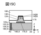
- FIG. 15B to 15D are schematic cross-sectional views showing an example of a method for manufacturing a semiconductor device.
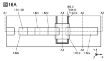
- FIG. 16A is a schematic plan view showing an example of a method for manufacturing a semiconductor device
- FIGS. 16B to 16D are schematic cross-sectional views showing an example of a method for manufacturing a semiconductor device.
- FIG. 17A is a schematic plan view showing an example of a method for manufacturing a semiconductor device
- FIGS. 17B to 17D are schematic cross-sectional views showing an example of a method for manufacturing a semiconductor device.
- FIG. 18A is a schematic plan view showing an example of a method for manufacturing a semiconductor device
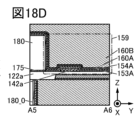
- FIGS. 18B to 18D are schematic cross-sectional views showing an example of a method for manufacturing a semiconductor device.
- FIG. 18A is a schematic plan view showing an example of a method for manufacturing a semiconductor device
- FIGS. 18B to 18D are schematic cross-sectional views showing an example of a method for manufacturing a semiconductor device.
- FIGS. 30A and 30B are schematic cross-sectional views showing an example of a method for manufacturing a semiconductor device.
- FIG. 31 is a schematic cross-sectional view showing an example of a method for manufacturing a semiconductor device.
- FIG. 32A is a perspective view illustrating a configuration example of a storage device
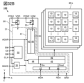
- FIG. 32B is a block diagram illustrating a configuration example of a semiconductor device.
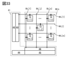
- FIG. 33 is a block diagram illustrating a configuration example of a storage device.
- FIG. 34 is a schematic cross-sectional diagram illustrating a configuration example of a storage device.
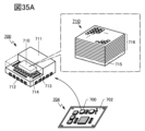
- 35A and 35B are diagrams showing an example of an electronic component.
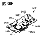
- 36A and 36B are diagrams showing an example of an electronic device, and FIGS.
- An example of a case where X and Y are electrically connected is an element that enables electrical connection between X and Y (for example, a switch, a transistor, a capacitive element, an inductor, a resistive element, a diode, a display device, light emitting device, and load) can be connected between X and Y.
- the switch has a function of controlling on/off. In other words, the switch is in a conductive state (on state) or non-conductive state (off state), and has a function of controlling whether or not current flows.
- both the element and the power line are placed between X and Y.
- VDD high power potential
- VSS low power potential
- GND ground potential
- X and Y are electrically connected.
- a transistor if the drain and source of the transistor are interposed between X and Y, it is defined that X and Y are electrically connected.
- a capacitive element when a capacitive element is placed between X and Y, it may or may not be specified that X and Y are electrically connected.
- a capacitive element in the configuration of a digital circuit or logic circuit, if a capacitive element is placed between X and Y, it may not be specified that X and Y are electrically connected.
- a capacitive element is disposed between X and Y, it may be specified that X and Y are electrically connected.
- X, Y, the source (sometimes translated as one of the first terminal or the second terminal) and the drain (sometimes translated as the other of the first terminal or the second terminal) of the transistor They are electrically connected to each other in the following order: X, the source of the transistor, the drain of the transistor, and Y. or "The source of the transistor is electrically connected to X, the drain of the transistor is electrically connected to Y, and X, the source of the transistor, the drain of the transistor, and Y are electrically connected in this order.” It can be expressed as "there is”.
- a “resistance element” can be, for example, a circuit element having a resistance value higher than 0 ⁇ or a wiring having a resistance value higher than 0 ⁇ . Therefore, in this specification and the like, a “resistance element” includes a wiring having a resistance value, a transistor in which a current flows between a source and a drain, a diode, or a coil. Therefore, the term “resistance element” may be translated into the terms “resistance", “load”, or "region having a resistance value”.
- the resistance value may be, for example, preferably 1 m ⁇ or more and 10 ⁇ or less, more preferably 5 m ⁇ or more and 5 ⁇ or less, and still more preferably 10 m ⁇ or more and 1 ⁇ or less. Further, for example, the resistance may be greater than or equal to 1 ⁇ and less than or equal to 1 ⁇ 10 9 ⁇ .
- a “capacitive element” refers to, for example, a circuit element having a capacitance value higher than 0F, a wiring region having a capacitance value higher than 0F, a parasitic capacitance, or It can be the gate capacitance of a transistor.
- the term “pair of conductors” in “capacitance” can be translated into “pair of electrodes,” “pair of conductive regions,” “pair of regions,” or “pair of terminals.” Further, the terms “one of a pair of terminals” and “the other of a pair of terminals” may be referred to as a first terminal and a second terminal, respectively.
- the value of the capacitance can be, for example, 0.05 fF or more and 10 pF or less. Further, for example, it may be set to 1 pF or more and 10 ⁇ F or less.
- a multi-gate structure transistor having two or more gate electrodes can be used as an example of a transistor.
- a multi-gate structure channel formation regions are connected in series, resulting in a structure in which a plurality of transistors are connected in series. Therefore, the multi-gate structure can reduce off-state current and improve the breakdown voltage (improve reliability) of the transistor.
- the multi-gate structure when operating in the saturation region, even if the voltage between the drain and source changes, the current between the drain and source does not change much, and the slope is flat. characteristics can be obtained. By utilizing voltage/current characteristics with a flat slope, it is possible to realize an ideal current source circuit or an active load with a very high resistance value. As a result, a differential circuit or a current mirror circuit with good characteristics can be realized.
- a node can be translated as a terminal, wiring, electrode, conductive layer, conductor, or impurity region depending on the circuit configuration and device structure. Furthermore, terminals, wiring, etc. can be referred to as nodes.
- Voltage refers to a potential difference from a reference potential.
- the reference potential is a ground potential (earth potential)
- “voltage” can be translated into “potential.” Note that the ground potential does not necessarily mean 0V.
- potential is relative, and as the reference potential changes, the potential applied to wiring, the potential applied to circuits, etc., the potential output from circuits, etc. also change.
- current refers to the phenomenon of charge movement (electrical conduction), and for example, the statement that "electrical conduction of a positively charged body is occurring” is replaced by “in the opposite direction, electrical conduction of a negatively charged body is occurring.” In other words, “electrical conduction is occurring.” Therefore, in this specification and the like, “current” refers to a charge movement phenomenon (electrical conduction) accompanying the movement of carriers, unless otherwise specified. Examples of carriers here include electrons, holes, anions, cations, and complex ions, and carriers differ depending on the system in which current flows (eg, semiconductor, metal, electrolyte, and in vacuum). Furthermore, the "direction of current” in wiring, etc.
- the terms “above” and “below” do not limit the positional relationship of the components to be directly above or below, and in direct contact with each other.
- electrode B does not need to be formed directly on insulating layer A, and there is no need to form another structure between insulating layer A and electrode B. Do not exclude things that contain elements.
- electrode B does not need to be formed on insulating layer A in direct contact with insulating layer A and electrode B. Do not exclude items that include other components between them.
- electrode B below the insulating layer A it is not necessary that the electrode B is formed under the insulating layer A in direct contact with the insulating layer A and the electrode B. Do not exclude items that include other components between them.
- words such as “row” and “column” may be used to describe components arranged in a matrix and their positional relationships. Further, the positional relationship between the components changes as appropriate depending on the direction in which each component is depicted. Therefore, the terms are not limited to those explained in the specification, etc., and can be appropriately rephrased depending on the situation. For example, the expression “row direction” may be translated into “column direction” by rotating the orientation of the drawing by 90 degrees.
- the words “film” and “layer” can be interchanged depending on the situation.
- the term “conductive layer” may be changed to the term “conductive film.”
- the term “insulating film” may be changed to the term “insulating layer.”
- the words “film” and “layer” may be omitted and replaced with other terms.
- the term “conductive layer” or “conductive film” may be changed to the term “conductor.”
- the term “insulating layer” or “insulating film” may be changed to the term "insulator.”
- the terms “electrode,” “wiring,” and “terminal” do not functionally limit these components.
- an “electrode” may be used as part of a “wiring” and vice versa.
- the terms “electrode” or “wiring” include cases where a plurality of “electrodes” or “wirings” are formed integrally.
- a “terminal” may be used as part of a “wiring” or “electrode,” and vice versa.
- the term “terminal” also includes cases in which one or more selected from “electrode,” “wiring,” and “terminal” are integrally formed.
- an “electrode” can be a part of a “wiring” or a “terminal,” and, for example, a “terminal” can be a part of a “wiring” or a “electrode.”
- the term “electrode,” “wiring,” or “terminal” may be replaced with the term “region” depending on the case.
- terms such as “wiring,” “signal line,” and “power line” can be interchanged depending on the case or the situation.
- the term “signal line” or “power line” may be changed to the term “wiring” in some cases.
- the term “power line” may be changed to the term "signal line”.
- the term “signal line” may be changed to the term "power line”.
- the term “potential” applied to the wiring may be changed to the term “signal”.
- the term “signal” may be changed to the term “potential”.
- timing charts may be used to explain the operating method of a semiconductor device.
- the timing charts used in this specification etc. show ideal operation examples, and the periods, magnitudes of signals (for example, potentials or currents), and timings described in the timing charts are is not limited unless otherwise specified.
- the timing charts described in this specification etc. may change the magnitude and timing of signals (e.g., potential or current) input to each wiring (including nodes) in the timing chart depending on the situation. It can be carried out. For example, even if two periods are written at equal intervals in the timing chart, the lengths of the two periods may be different from each other. Also, for example, even if one period is long and the other short, the lengths of both periods may be equal, or one period may be short. In some cases, the other period may be made longer.
- metal oxide refers to a metal oxide in a broad sense.
- Metal oxides are classified into oxide insulators, oxide conductors (including transparent oxide conductors), oxide semiconductors (also referred to as oxide semiconductors or simply OS), and the like.
- oxide semiconductors also referred to as oxide semiconductors or simply OS
- the metal oxide when a metal oxide is included in a channel formation region of a transistor, the metal oxide is sometimes referred to as an oxide semiconductor.
- a metal oxide can constitute a channel forming region of a transistor having at least one of an amplification effect, a rectification effect, and a switching effect, the metal oxide is called a metal oxide semiconductor. can do.
- OS transistor it can be referred to as a transistor including a metal oxide or an oxide semiconductor.
- metal oxides containing nitrogen may also be collectively referred to as metal oxides.
- a metal oxide containing nitrogen may be referred to as a metal oxynitride.
- semiconductor impurities refer to, for example, substances other than the main components that constitute the semiconductor layer.
- an element having a concentration of less than 0.1 atomic % is an impurity.
- impurities that change the characteristics of the semiconductor include, for example, group 1 elements, group 2 elements, group 13 elements, group 14 elements, and group 15 elements.
- transition metals other than the main components in particular, for example, hydrogen (also present in water), lithium, sodium, silicon, boron, phosphorus, carbon, and nitrogen.
- impurities that change the characteristics of the semiconductor include, for example, Group 1 elements, Group 2 elements, Group 13 elements, and Group 15 elements (however, oxygen and hydrogen are not included). There is).
- a switch refers to a switch that is in a conductive state (on state) or a non-conductive state (off state) and has the function of controlling whether or not current flows.
- a switch refers to a device that has the function of selecting and switching a path through which current flows. Therefore, a switch may have two, three or more terminals through which current flows, in addition to the control terminal.
- an electrical switch, a mechanical switch, etc. can be used. In other words, the switch is not limited to a specific type as long as it can control the current.
- electrical switches include transistors (e.g., bipolar transistors, MOS transistors, etc.), diodes (e.g., PN diodes, PIN diodes, Schottky diodes, MIM (Metal Insulator Metal) diodes, and MIS (Metal Insulator Semiconductor)). diode , and diode-connected transistors), or logic circuits that combine these.
- the "conducting state" of the transistor means, for example, a state in which the source and drain electrodes of the transistor can be considered to be electrically short-circuited, or a state in which there is no current between the source and drain electrodes. A state in which the flow of water is possible.
- non-conducting state of a transistor refers to a state in which the source electrode and drain electrode of the transistor can be considered to be electrically disconnected. Note that when the transistor is operated as a simple switch, the polarity (conductivity type) of the transistor is not particularly limited.
- parallel refers to a state in which two straight lines are arranged at an angle of -10° or more and 10° or less. Therefore, the case where the angle is greater than or equal to -5° and less than or equal to 5° is also included.
- substantially parallel or “substantially parallel” refers to a state in which two straight lines are arranged at an angle of -30° or more and 30° or less.
- perpendicular refers to a state in which two straight lines are arranged at an angle of 80° or more and 100° or less. Therefore, the case where the angle is 85° or more and 95° or less is also included.
- substantially perpendicular or “approximately perpendicular” refers to a state in which two straight lines are arranged at an angle of 60° or more and 120° or less.
- each embodiment can be appropriately combined with the structure shown in other embodiments to form one embodiment of the present invention. Further, when a plurality of configuration examples are shown in one embodiment, it is possible to combine the configuration examples with each other as appropriate.
- content (or even part of the content) described in one embodiment may be different from other content (or even part of the content) described in that embodiment and one or more other implementations. It is possible to apply, combine, or replace at least one content with the content described in the form (or even a part of the content).
- the code when the same code is used for multiple elements, especially when it is necessary to distinguish between them, the code includes an identifying symbol such as "_1", “[n]”, “[m,n]”, etc. In some cases, the symbol may be added to the description. In addition, in the drawings, etc., when a code for identification such as “_1”, “[n]”, “[m,n]”, etc. is added to the code, when there is no need to distinguish it in this specification etc. In some cases, no identification code is written.
- FIG. 1 is a circuit diagram illustrating a configuration example of a semiconductor device DEV that is one embodiment of the present invention.
- the semiconductor device DEV includes, for example, a memory layer ALYa and a memory layer ALYb. Note that in FIG. 1, the storage layer ALYb is located above the storage layer ALYa.
- Each of the storage layer ALYa and the storage layer ALYb has a plurality of memory cells.
- a plurality of memory cells are arranged in an array.
- FIG. 1 it is assumed that memory cells MCa are arranged in a matrix of m rows and n columns (m is an integer greater than or equal to 1, and n is an integer greater than or equal to 1) in the memory layer ALYa. .
- memory cells MCb are arranged in a matrix of m rows and n columns (m is an integer greater than or equal to 1, and n is an integer greater than or equal to 1) in the memory layer ALYb. shall be taken as a thing.
- a memory cell located in the first row and first column of the matrix of the storage layer ALYa is referred to as a memory cell MCa[1,1], and for example, The memory cell located in the mth row and nth column of the matrix of the storage layer ALYb is written as a memory cell MCb[m,n].
- memory cells located in the i-th row and j-th column of the matrix of the storage layer ALYa i is an integer from 1 to m, and j is an integer from 1 to n-1) MCa[i,j] and a memory cell MCa[i,j+1] located in the i-th row and j+1-th column are illustrated.
- memory cell MCb[i,j] located in the i-th row and j-th column of the matrix of the storage layer ALYb, and memory cell MCb[i, j+1] located in the i-th row and j+1st column, is illustrated.
- memory cell MCa and memory cell MCb have similar circuit configurations. Therefore, in this specification and the drawings, when describing matters common to each of memory cell MCa and memory cell MCb, each of memory cell MCa and memory cell MCb will be described as memory cell MC.
- the number of rows and the number of columns of the matrix of the storage layer ALYa and the number of rows and the number of columns of the matrix of the storage layer ALYb may be the same or different from each other.
- the memory cell MC shown in FIG. 1 is an example of a memory cell called a gain cell, and includes a transistor M1, a transistor M2, a transistor M3, and a capacitive element C1.
- the configuration of the memory cell MC using OS transistors for each of the transistors M1 to M3 is sometimes referred to as NOSRAM (registered trademark) (Nonvolatile Oxide Semiconductor Random Access Memory).
- examples of metal oxides included in the channel formation region of the OS transistor include indium oxide, gallium oxide, and zinc oxide.
- the metal oxide has one or more selected from indium, element M, and zinc.
- element M is gallium, aluminum, silicon, boron, yttrium, tin, copper, vanadium, beryllium, titanium, iron, nickel, germanium, zirconium, molybdenum, lanthanum, cerium, neodymium, hafnium, tantalum, tungsten, cobalt, One or more selected from magnesium and antimony.
- the element M is preferably one or more selected from aluminum, gallium, yttrium, and tin.
- an oxide containing indium (In), gallium (Ga), and zinc (Zn) also referred to as IGZO
- an oxide also referred to as IAGZO
- IAGZO oxide containing indium (In), aluminum (Al), gallium (Ga), and zinc (Zn).
- IAGZO oxide containing indium (In), aluminum (Al), gallium (Ga), and zinc (Zn).
- transistors other than OS transistors may be applied to the transistors M1 to M3.
- transistors having silicon in their channel formation regions (hereinafter referred to as Si transistors) can be used as the transistors M1 to M3.
- silicon for example, single crystal silicon, amorphous silicon (sometimes referred to as hydrogenated amorphous silicon), microcrystalline silicon, or polycrystalline silicon (including low-temperature polycrystalline silicon) can be used.
- the transistors M1 to M3 include, for example, a transistor whose channel formation region contains germanium, zinc selenide, cadmium sulfide, gallium arsenide, indium phosphide, gallium nitride, Alternatively, a transistor in which a channel formation region includes a compound semiconductor such as silicon germanium, a transistor in which a carbon nanotube is included in a channel formation region, or a transistor in which an organic semiconductor is included in a channel formation region can be used.
- transistors M1 to M3 shown in FIG. 1 are n-channel transistors, they may be p-channel transistors depending on the situation or case. Further, when an n-channel transistor is replaced with a p-channel transistor, it is necessary to appropriately change the potential input to the memory cell MC so that the memory cell MC operates normally. Note that this applies not only to FIG. 1 but also to transistors described in other parts of the specification and transistors illustrated in other drawings. Furthermore, in this embodiment, the configuration of the memory cell MC will be described with transistors M1 to M3 as n-channel transistors.
- the transistors M1 to M3 operate in a saturation region when each of them is in an on state.
- the voltage between the gate and source of any one of transistors M1 to M3 is constant, the current flowing between the source and drain of any one of the transistors is such that the current flowing between the source and drain of any one of the transistors operates in the linear region. It will be bigger than when you do it. In this way, by increasing the amount of current, the signal transmission speed increases, and as a result, the operating speed of the circuit can be increased.
- transistors M1 to M3 Note that the above description of the transistors is applicable not only to the transistors M1 to M3, but also to transistors described in other parts of the specification and transistors described in the drawings.
- the first terminal of transistor M1 is electrically connected to the gate of transistor M2 and the first terminal of capacitive element C1. It is connected. Further, the first terminal of the transistor M2 is electrically connected to the first terminal of the transistor M3.
- the second terminal of the transistor M1 is electrically connected to the wiring WRBLa[j]
- the second terminal of the transistor M2 is electrically connected to the wiring SLa[j].
- the second terminal of the transistor M3 is electrically connected to the wiring WRBLa[j+1].
- the gate of the transistor M1 is electrically connected to the wiring WWLa[i]
- the second terminal of the capacitive element C1 is electrically connected to the wiring CLa[i]
- the gate of the transistor M3 is electrically connected to the wiring WWLa[i]. i].
- the second terminal of the transistor M1 is electrically connected to the wiring WRBLa[j+1], and the second terminal of the transistor M2 is electrically connected to the wiring SLa[j+1].
- the second terminal of the transistor M3 is electrically connected to the wiring WRBLa[j+2].
- the gate of the transistor M1 is electrically connected to the wiring WWLa[i]
- the second terminal of the capacitive element C1 is electrically connected to the wiring CLa[i]
- the gate of the transistor M3 is electrically connected to the wiring WWLa[i]. i].
- the back gate of the transistor M1 is electrically connected to, for example, a wiring extending below the storage layer ALYa. may be connected (not shown).
- the wiring WWLa[i] functions as a write word line for the memory cell MCa[i,j] and the memory cell MCa[i,j+1] included in the storage layer ALYa, for example.
- the wiring WWLa[i] functions as a wiring that transmits a selection signal (which may be a current, a variable potential, or a pulse voltage) for selecting the memory cell MCa to be written.
- a selection signal which may be a current, a variable potential, or a pulse voltage
- the wiring WWLa[i] may function as a wiring that applies a fixed potential depending on the situation.
- the wiring RWLa[i] functions as a read word line for the memory cell MCa[i,j] and the memory cell MCa[i,j+1] included in the storage layer ALYa, for example.
- the wiring RWLa[i] functions as a wiring that transmits a selection signal (which may be a current, a variable potential, or a pulse voltage) for selecting the memory cell MCa to be read.
- a selection signal which may be a current, a variable potential, or a pulse voltage
- the wiring RWLa[i] may function as a wiring that applies a fixed potential depending on the situation.
- the wiring WRBLa[j] functions as a write bit line for the memory cell MCa[i,j] included in the storage layer ALYa, for example.
- the wiring WRBLa[j] functions as a wiring that transmits write data to the selected memory cell MCa[i,j].
- the wiring WRBLa[j+1] functions as a write bit line for the memory cell MCa[i,j+1] included in the storage layer ALYa.
- the wiring WRBLa[j+1] functions as a wiring that transmits write data to the selected memory cell MCa[i, j+1].
- the wiring WRBLa[j+1] also functions as a read bit line for the memory cell MCa[i,j] included in the storage layer ALYa, for example.
- the wiring WRBLa[j+1] functions as a wiring that transmits read data from the selected memory cell MCa[i,j].
- the wiring WRBLa[j+2] functions as a write bit line for the memory cell MCa[i,j+1] included in the storage layer ALYa.
- the wiring WRBLa[j+2] functions as a wiring that transmits read data from the selected memory cell MCa[i, j+1].
- the wiring WRBLa[j] is, for example, a memory cell MCa[i, j-1] (not shown in FIG. 1) included in the storage layer ALYa. functions as a read bit line for Further, the wiring WRBLa[j+1] is, for example, a memory cell MCa[i, j+2] (not shown in FIG. 1) included in the storage layer ALYa. functions as a write bit line for
- the wiring WRBLa functions as a write bit line for one of the adjacent memory cells via the wiring WRBLa, and functions as a read bit line for the other adjacent memory cell via the wiring WRBLa.
- the wiring WRBLa[j] to the wiring WRBLa[j+2] may function as a wiring that provides a fixed potential depending on the situation.
- the wiring SLa[j] functions as a wiring that applies a fixed potential to the memory cell MCa[i,j] included in the storage layer ALYa, for example. Further, the wiring SLa[j+1] functions as a wiring that applies a fixed potential to the memory cell MCa[i,j+1] included in the storage layer ALYa, for example. Note that each of the wiring SLa[j] and the wiring SLa[j+1] may function as a wiring that provides a variable potential depending on the situation.
- the wiring CLa[i] functions as a wiring that applies a fixed potential to, for example, the memory cell MCa[i,j] and the memory cell MCa[i,j+1] included in the storage layer ALYa. Note that the wiring CLa[i] may function as a wiring that provides a variable potential depending on the situation.
- the configuration of the storage layer ALYb can be the same as that of the storage layer ALYa. Therefore, in the above description of the configuration of memory cell MCa, the configuration of memory cell MCb is such that wiring WWLa[i] is replaced with wiring WWLb[i], wiring RWLa[i] is replaced with wiring RWLb[i], and wiring WRBLa[i] is replaced with wiring WWLb[i].
- the back gate of the transistor M1 included in each of the memory cell MCb[i,j] and the memory cell MCb[i,j+1] arranged in the storage layer ALYb is, for example, extended to the storage layer ALYa. It is electrically connected to the wiring CLa.
- the second terminal of the capacitive element C1 included in each of the memory cell MCb[i,j] and the memory cell MCb[i,j+1] arranged in the storage layer ALYb is, for example, located above the storage layer ALYb. (not shown) may be electrically connected to wiring extending in the storage layer of the memory layer.
- writing data to the memory cell MC and reading data from the memory cell MC in the semiconductor device DEV shown in FIG. 1 will be described.
- writing of data to the memory cell MCa[i,j] of the storage layer ALYa of the semiconductor device DEV and reading of data from the memory cell MCa[i,j] will be described.
- a first potential (eg, ground potential) is applied to the wiring CLa[i].
- a high level potential is applied to the wiring WWLa[i] to turn on the transistor M1 included in the memory cell MCa[i,j], and the wiring WWLa[1] to the wiring other than the wiring WWLa[i] is
- a low level potential is applied to WWLa[m] to turn off the transistors M1 included in memory cells MCa from the first row to the m-th row other than the i-th row.
- a low level potential is applied to the wirings RWLa[1] to RWLa[m] to turn off the transistor M3 included in the memory cell MCa[i,j].
- writing data to or reading data from other memory cells MCa can be performed in the same manner as described above.
- circuit configuration of the semiconductor device of one embodiment of the present invention is not limited to the configuration in FIG. 1.
- the circuit configuration of the semiconductor device may be changed depending on the situation.
- the wiring SLa[j] and the wiring SLa[j+1] extend in the column direction of the matrix of the storage layer ALYa, but the wiring SLa[j] and the wiring SLa[j+1] may extend in the row direction of the matrix of the storage layer ALYa.
- a wiring extending in one of the row direction or column direction may be changed to extend in the other row direction or column direction.
- FIG. 2 is a schematic cross-sectional view showing a configuration example of a semiconductor device DEV that is one embodiment of the present invention.
- the semiconductor device DEV has a configuration in which not only a storage layer ALYa and a storage layer ALYb but also a storage layer ALYc above the storage layer ALYb is provided.
- the storage layer ALYc includes a memory cell MCc having the same configuration as the memory cell MCa and the memory cell MCb.
- the semiconductor device DEV has a configuration in which storage layers are also provided below the storage layer ALYa and above the storage layer ALYc.
- FIG. 3 is a schematic cross-sectional view focusing on the memory layer ALYa and the memory layer ALYb in the configuration example of the DEV of the semiconductor device in FIG. and symbols indicating constituent elements of the storage layer ALYb.
- FIG. 3 shows a configuration example in which the memory layer ALYa is provided on the insulator 122a, the insulator 122b is provided on the memory layer ALYa, and the memory layer ALYb is provided on the insulator 122b. Note that details of the insulator 122a and the insulator 122b will be described later.
- the X direction shown in FIGS. 2 to 22D is parallel to the channel length direction of each of the transistors M1, M2, and M3, the Y direction is perpendicular to the X direction, and the Z direction is parallel to the X direction and the Y direction. perpendicular to the direction. Further, the X direction, Y direction, and Z direction shown in FIGS. 2 to 22D are right-handed.
- FIG. 4 is a schematic perspective view showing a partial configuration example of the storage layer ALYa of the semiconductor device DEV of FIG. 3.
- the insulator 122b, the insulator 180, the insulator 180_0, and the insulator 175 are not illustrated in order to make the structure of the storage layer ALYa easier to see. Note that details of the insulator 122b, the insulator 180, the insulator 180_0, and the insulator 175 will be described later.
- the memory cell MCa includes the transistor M1, the transistor M2, the transistor M3, and the capacitive element C1.
- each of the transistors M1 to M3 is an OS transistor, as an example. That is, each of the semiconductor layers of the transistors M1 to M3 contains a metal oxide.
- each of the transistors M1 to M3 includes an insulator 124 and an oxide 130.
- the transistor M1 includes a conductor 142a, a conductor 142d, a conductor 160_2, a conductor 170_0, a conductor 160_0, an insulator 153_2, and an insulator 154_2.
- the transistor M2 includes a conductor 142b, a conductor 142c, a conductor 160_3, an insulator 153_3, and an insulator 154_3.
- the transistor M3 includes a conductor 142c, a conductor 142d, a conductor 160_4, an insulator 153_4, and an insulator 154_4.
- the capacitive element C1 includes a conductor 142a, a conductor 160_1, an insulator 153_1, and an insulator 154_1.
- each of the conductors 160_2 to 160_4 is provided to overlap with the oxide 130.
- the conductors 160_2 to 160_4 are arranged in order in the X direction so as not to overlap each other.
- the conductor 160_2 functions as the gate of the transistor M1, the conductor 160_3 functions as the gate of the transistor M2, and the conductor 160_4 functions as the gate of the transistor M3.
- each gate may be referred to as a first gate.
- each of the conductors 160_2 to 160_4 may be referred to as a gate electrode or a first gate electrode.
- the conductor 160_2 functions as the wiring WWLa[i] in FIG. 1, for example.
- the conductor 160_4 functions as the wiring RWLa[i] in FIG. 1, for example.
- the insulator 153_2 and the insulator 154_2 function as a first gate insulating film in the transistor M1. Further, the insulator 153_3 and the insulator 154_3 function as a first gate insulating film in the transistor M2. Further, the insulator 153_4 and the insulator 154_4 function as a first gate insulating film in the transistor M3.
- the insulator 124 is provided on the insulator 122a. Further, the insulator 122a and the insulator 124 function as a second gate insulating film in the transistor M1.
- the oxide 130 is provided on the insulator 124. Further, the oxide 130 functions as a semiconductor included in the channel formation regions of the transistors M1 to M3.
- each of the conductor 160_0 and the conductor 170_0 function as a back gate (sometimes referred to as a second gate) in the transistor M1. Therefore, in this specification and the like, each of the conductor 160_0 and the conductor 170_0 may be referred to as a back gate electrode or a second gate electrode. Further, the conductor 160_0 and the conductor 170_0 also function as one of a pair of electrodes of a capacitive element included in a memory cell in a storage layer located below the storage layer ALYa.
- FIG. (sometimes referred to as a layered film or an interlayer film).
- the conductor 142a is provided, for example, on the top surface and side surfaces of the oxide 130, and in a region that does not overlap with the oxide 130. Specifically, it is provided on a part of the oxide 130 and a part of the insulator 122a. Furthermore, the conductor 142d is provided on a portion of the oxide 130, for example. In particular, the conductor 142a and the conductor 142d are physically separated from each other by the insulator 153_2 and the insulator 154_2. The conductor 142a functions as one of the source or drain of the transistor M1, and the conductor 142d functions as the other of the source or drain of the transistor M1.
- the conductor 142c is provided on a portion of the oxide 130, for example.
- the conductor 142d is provided on a portion of the oxide 130, for example.
- the conductor 142c and the conductor 142d are physically separated from each other by the insulator 153_4 and the insulator 154_4.
- the conductor 142c functions as one of the source or drain of the transistor M3, and the conductor 142d functions as the other of the source or drain of the transistor M3.
- a conductor 170_0 is provided below the memory layer ALYa. Further, the oxide 130 is provided on the region including the conductor 170_0. Further, a conductor 142a and a conductor 142d are provided so as to partially cover the oxide 130. Further, a conductor 160_2 is provided above a region between the conductor 142a and the conductor 142d, including the area where the conductor 170_0 and the oxide 130 overlap. This forms transistor M1. Furthermore, a conductor 170_2 is provided on the conductor 160_2.
- an opening PLa provided in an interlayer film (not shown) is located on the conductor 142a. Further, an opening PLd provided in the interlayer film is located on the conductor 142d.
- a conductor 170_3 is embedded in the opening PLa, and a conductor 170_5 is embedded in the opening PLd.
- the conductor 170_3 embedded in the opening PLa and the conductor 170_5 embedded in the opening PLd function as wiring or a plug.
- the conductor 170_5 extends along the Y direction.
- a conductor 142b and a conductor 142c are provided so as to cover a part of the oxide 130.
- a conductor 160_3 is provided in a region between the conductor 142b and the conductor 142c, which overlaps with the oxide 130. This forms transistor M2.
- a conductor 170_3 is provided on the conductor 160_3.
- an insulator (not shown) is provided on a part of the conductor 142a, and a conductor 160_1 is provided on the insulator.
- a capacitive element C1 is formed in which a portion of the conductor 142a and the conductor 160_1 each serve as a pair of electrodes.
- a conductor 170_1 is provided on the conductor 160_1.
- the conductor 170_1 included in the memory layer ALYa also functions as a back gate electrode of the transistor M1 in the memory layer ALYb.
- the memory layer ALYa includes a conductor 142e, a conductor 142f, and a conductor 142g extending in the row direction. Further, the conductor 142a of the transistor M1 also has a region extending in the row direction. Note that the conductor 142e, the conductor 142f, and the conductor 142g can be formed at the same time as the conductor 142a, the conductor 142b, the conductor 142c, and the conductor 142d.
- an opening PLc provided in an interlayer film (not shown) is located above the conductor 142e. Furthermore, a conductor 170_4 is embedded in the opening PLc. Thereby, the conductor 170_4 embedded in the opening PLc functions as a wiring or a plug. Therefore, the conductor 142e and the conductor 160_4 of the transistor M3 are electrically connected to each other.
- an opening PLe provided in an interlayer film is located on the conductor 142g. Furthermore, a conductor 170_1 is embedded in the opening PLe. Thereby, the conductor 170_1 embedded in the opening functions as a wiring or a plug. Therefore, the conductor 142g and the conductor 160_1 of the capacitive element C1 are electrically connected to each other.
- the conductor 142e functions as a wiring RWLa[i] or a wiring RWLa[i+1] extending in the row direction.
- the conductor 142f functions as the wiring WWLa[i] or the wiring WWLa[i+1] extending in the row direction.
- an insulator is provided between the oxide 130 and the conductor 160_2, between the oxide 130 and the conductor 160_3, and between the oxide 130 and the conductor 160_4.
- the insulator may function as a first gate insulating film (sometimes referred to as a gate insulating film or a front gate insulating film).
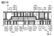
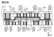
- the memory layer ALYa includes an insulator 124 located on the insulator 122a in a region that overlaps with the conductor 160_0, and an oxide 130 (oxide 130a and oxide 130b) located on the upper surface of the insulator 124.
- Conductors 142a (conductors 142a1 and 142a2) located on the top and side surfaces of the oxide 130; conductors 142b (conductors 142b1 and 142b2) located on the top and side surfaces of the oxide 130;
- the conductor 142c (conductor 142c1 and conductor 142c2) is located on the top surface of oxide 130, and the conductor 142d (conductor 142d1 and conductor 142d2) is located on the top surface of oxide 130.
- the memory layer ALYa includes an insulator 153_2 located on the upper surface and side surfaces of the oxide 130, an insulator 154_2 located on the upper surface of the insulator 153_2, and a conductor 160_2 (conductor 160a_2 located on the upper surface of the insulator 154_2). and a conductor 160b_2). Furthermore, the memory layer ALYa includes a conductor 170_2 (a conductor 170a_2 and a conductor 170b_2) located on the upper surface of the insulator 153_2, the upper surface of the insulator 154_2, the upper surface of the conductor 160_2, and the upper surface of the insulator 180.
- the storage layer ALYa also includes an insulator 153_3 located on the top surface and side surfaces of the oxide 130, an insulator 154_3 located on the top surface of the insulator 153_3, and a conductor 160_3 (conductor 160a_3 located on the top surface of the insulator 154_3). and a conductor 160b_3). Furthermore, the memory layer ALYa includes a conductor 170_3 (a conductor 170a_3 and a conductor 170b_3) located on the upper surface of the insulator 153_3, the upper surface of the insulator 154_3, the upper surface of the conductor 160_3, and the upper surface of the insulator 180.
- the insulator 180 has an opening in a region that overlaps with the conductor 142a and does not overlap with the oxide 130. Further, a conductor 170_3 (conductor 170a_3 and conductor 170b_3) is located inside the opening and on the upper surface of the insulator 180. In the memory layer ALYa, the insulator 180 also has an opening in a region overlapping the conductor 142d. Further, a conductor 170_5 (conductor 170a_5 and conductor 170b_5) is located inside the opening and on the upper surface of the insulator 180.
- the insulator 180 and the insulator 175 are provided with an opening 158_2 that reaches the oxide 130b.
- the opening 158_2 has a region that overlaps with the oxide 130b.
- the insulator 175 has an opening that overlaps the opening that the insulator 180 has. That is, the opening 158_2 includes an opening that the insulator 180 has and an opening that the insulator 175 has.
- an insulator 153_2, an insulator 154_2, and a conductor 160_2 are arranged within the opening 158_2.
- the conductor 160_2 has a region that overlaps with the oxide 130b via the insulator 153 and the insulator 154.
- a conductor 160_2, an insulator 153_2, and an insulator 154_2 are provided between the conductor 142a and the conductor 142d.
- the insulator 154_2 has a region in contact with the side surface of the conductor 160_2 and a region in contact with the bottom surface of the conductor 160_2. Note that, as shown in FIG. 8C, in the region of the opening 158_2 that does not overlap with the oxide 130, the insulator 122a and the insulator 153_2 are in contact with each other.
- the insulator 180 and the insulator 175 are provided with an opening 158_3 that reaches the oxide 130b, and the transistor M3 is It is assumed that in the formed region, the insulator 180 and the insulator 175 are provided with an opening 158_4 that reaches the oxide 130b. It can be said that the opening 158_3 and the opening 158_4 include an opening that the insulator 180 has and an opening that the insulator 175 has, similar to the opening 158_2.
- an insulator 153_3, an insulator 154_3, and a conductor 160_3 are arranged in the opening 158_3, and an insulator 153_4, an insulator 154_4, and a conductor 160_4 are arranged in the opening 158_4.
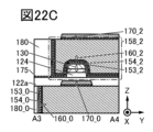
- the cross-sectional view of the channel width of the transistor M1 shown in FIG. 8C can be referred to.
- the oxide 130 preferably includes an oxide 130a disposed on the insulator 124 and an oxide 130b disposed on the oxide 130a.
- the oxide 130a By having the oxide 130a below the oxide 130b, diffusion of impurities from a structure formed below the oxide 130a to the oxide 130b can be suppressed.
- the oxide 130 has a structure in which two layers, the oxide 130a and the oxide 130b, are laminated, but the present invention is not limited to this.
- a single layer of the oxide 130b or a stacked structure of three or more layers may be used, or each of the oxide 130a and the oxide 130b may have a stacked structure.
- the transistor M1 includes an oxide 130 that functions as a semiconductor layer, a conductor 160_2 that functions as a first gate (also referred to as a gate, top gate, or front gate) electrode, and a second gate (back gate).
- a conductor 170_0 that functions as an electrode
- a conductor 142a that functions as either a source electrode or a drain electrode
- a conductor 142d that functions as the other source electrode or drain electrode.
- It also includes an insulator 153_2 and an insulator 154_2 that function as a first gate insulator.
- It also includes an insulator 122a and an insulator 124 that function as a second gate insulator.
- the gate insulator is sometimes called a gate insulating layer or a gate insulating film.
- at least a portion of the region of the oxide 130 that overlaps with the conductor 160_2 functions as a channel formation region.
- the first gate electrode and the first gate insulating film are arranged in the opening 158_2 formed in the insulator 180 and the insulator 175. That is, the conductor 160_2, the insulator 154_2, and the insulator 153_2 are arranged within the opening 158_2.
- the transistor M2 includes an oxide 130 that functions as a semiconductor layer, a conductor 160_3 that functions as a gate (also referred to as a top gate or front gate) electrode, and a conductor 142b that functions as either a source electrode or a drain electrode.
- a conductor 142c functioning as the other of a source electrode and a drain electrode. It also includes an insulator 153_3 and an insulator 154_3 that function as gate insulators. It also includes an insulator 122a and an insulator 124. Furthermore, at least a portion of the region of the oxide 130 that overlaps with the conductor 160_3 functions as a channel formation region.
- the transistor M3 includes an oxide 130 that functions as a semiconductor layer, a conductor 160_4 that functions as a gate (also referred to as a top gate or front gate) electrode, and a conductor 142c that functions as either a source electrode or a drain electrode.
- a conductor 142d functioning as the other of a source electrode and a drain electrode. It also includes an insulator 153_4 and an insulator 154_4 that function as gate insulators. It also includes an insulator 122a and an insulator 124. Furthermore, at least a portion of the region of the oxide 130 that overlaps with the conductor 160_4 functions as a channel formation region.
- the capacitive element C1 includes a conductor 142a that functions as a lower electrode, an insulator 153_1 and an insulator 154_1 that function as a dielectric, and a conductor 160_1 that functions as an upper electrode. That is, the capacitive element C1 constitutes an MIM (Metal-Insulator-Metal) capacitor.
- MIM Metal-Insulator-Metal
- the upper electrode and dielectric of the capacitive element C1 are arranged within the opening 159 formed in the insulator 180 and the insulator 175. That is, the conductor 160_1, the insulator 153_1, and the insulator 154_1 are arranged within the opening 159.
- the conductor 170_3 is also located on the insulator 180, on the insulator 153_3, on the insulator 154_3, and on the conductor 160_3. Therefore, the conductor 170_3 and the conductor 160_3 are electrically connected to each other.
- the conductor 170_2 is located on the insulator 180, on the insulator 153_2, on the insulator 154_2, and on the conductor 160_2. Therefore, the conductor 170_2 and the conductor 160_2 are electrically connected to each other. Further, the conductor 170_2 functions as a wiring or a plug.
- the conductor 170_4 is located on the insulator 180, on the insulator 153_4, on the insulator 154_4, and on the conductor 160_4. Therefore, the conductor 170_4 and the conductor 160_4 are electrically connected to each other. Further, the conductor 170_4 functions as a wiring or a plug.
- the storage layer ALYa shown in this embodiment and including the transistor M1, the transistor M2, the transistor M3, and the capacitor C1 can be used for a storage device.
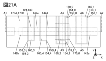
- each A indicates a schematic plan view.
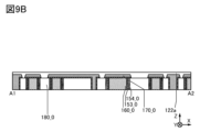
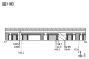
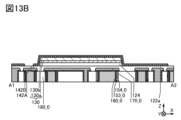
- B in each figure is a schematic cross-sectional view corresponding to a portion taken along a dashed-dotted line A1-A2 shown in each A, and is also a schematic cross-sectional view in the channel length direction of the transistors M1 to M3.
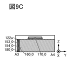
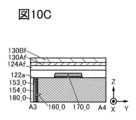
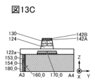
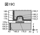
- C in each figure is a schematic cross-sectional view corresponding to a portion taken along a dashed-dotted line A3-A4 shown in each A, and is also a schematic cross-sectional view in the channel width direction of the transistor M1.
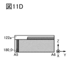
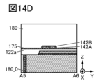
- D in each figure is a schematic cross-sectional view of a portion taken along a dashed-dotted line A5-A6 shown in each A. Note that in the schematic plan view A of each figure, some elements are omitted for clarity.
- an insulating material for forming an insulator, a conductive material for forming a conductor, or a semiconductor material for forming a semiconductor includes a sputtering method, a CVD method, an MBE (Molecular Beam Epitaxy) method,
- the film can be formed using a film forming method such as a PLD method or an ALD method as appropriate.
- a substrate (not shown) is prepared, and a memory layer below the memory layer ALYa is formed on the substrate.
- a memory layer below the memory layer ALYa is formed on the substrate.
- an insulator 180_0, an insulator 153_0, an insulator 154_0, a conductor 160_0, a conductor 170_0, and an insulator 122a are formed on the substrate (see FIGS. 9A to 9D). Note that in FIGS.
- transistors included in the memory layer below the memory layer ALYa include transistors included in the memory layer below the memory layer ALYa.
- the first gate electrode and first gate insulating film of each of transistors M1 to M3 are also illustrated.
- the methods for forming the insulator 180_0, the insulator 153_0, the insulator 154_0, and the conductor 160_0 will be described later.
- the method for forming the conductors 160_4 will be considered (see FIGS. 14A to 19D).
- first gate electrode and first gate insulating film of each of the transistors M1 to M3 included in the storage layer below the storage layer ALYa can also be formed in the same manner as described above. Further, the first gate insulating films of each of the transistors M1 to M3 can be formed simultaneously with the insulator 153_0 and the insulator 154_0. Furthermore, the first gate electrodes of each of the transistors M1 to M3 can be formed at the same time as the conductor 160_0.
- a second conductive film to become the conductor 170_0 is formed on the upper surface of each of the insulator 180_0, the insulator 153_0, the insulator 154_0, and the conductor 160_0, and the second conductive film is processed using a lithography method. By doing so, the conductor 170_0 can be formed. Note that regarding the formation of the conductor 170_0, a method for forming conductors 170_1 to 170_5, which will be described later, will be referred to (see FIGS. 20A to 22D).
- An insulator containing oxides of one or both of aluminum and hafnium has barrier properties against oxygen, hydrogen, and water. Since the insulator 122a has barrier properties against hydrogen and water, hydrogen and water contained in the structures provided around the transistors M1 to M3 diffuse into the inside of the transistors M1 to M3 through the insulator 122a. Therefore, the generation of oxygen vacancies in the oxide 130 can be suppressed.
- the insulator 122a can be formed using a film forming method such as a sputtering method, a CVD method, an MBE method, a PLD method, or an ALD method.
- hafnium oxide is formed as the insulator 122a by using an ALD method.
- a high-k material with a high dielectric constant may be used as the insulating material used for the insulator 122a.
- high-k materials with a high dielectric constant include, in addition to the above-mentioned hafnium oxide, one or two selected from aluminum, gallium, yttrium, zirconium, tungsten, titanium, tantalum, nickel, germanium, and magnesium. Examples include metal oxides containing the above.
- the insulator 122a may be an insulator containing an oxide of one or both of aluminum and hafnium, such as aluminum oxide, hafnium oxide, or an oxide containing aluminum and hafnium (hafnium aluminate). .
- the heat treatment may be performed at a temperature of 250°C or higher and 650°C or lower, preferably 300°C or higher and 500°C or lower, and more preferably 320°C or higher and 450°C or lower.
- the heat treatment is performed in an atmosphere of nitrogen gas or inert gas, or an atmosphere containing 10 ppm or more, 1% or more, or 10% or more of oxidizing gas.
- the oxygen gas content may be about 20%.
- the heat treatment may be performed under reduced pressure.
- heat treatment is performed in an atmosphere of nitrogen gas or inert gas, and then heat treatment is performed in an atmosphere containing 10 ppm or more, 1% or more, or 10% or more of oxidizing gas to compensate for the desorbed oxygen. Good too.
- the gas used in the heat treatment is preferably highly purified.
- the amount of water contained in the gas used in the heat treatment may be 1 ppb or less, preferably 0.1 ppb or less, and more preferably 0.05 ppb or less.
- the heat treatment is performed at a temperature of 400° C. for 1 hour at a flow rate ratio of nitrogen gas and oxygen gas of 4:1 after the insulator 122a is formed.
- impurities such as water or hydrogen contained in the insulator 122a can be removed.
- a part of the insulator 122a may be crystallized by the heat treatment.
- the heat treatment can also be performed at a timing such as after the insulator 124 is formed.
- the oxide film 130Bf when forming the oxide film 130Bf by sputtering, if the proportion of oxygen contained in the sputtering gas is more than 30% and less than 100%, preferably more than 70% and less than 100%, oxygen-excess oxidation occurs. A physical semiconductor is formed. A transistor using an oxygen-rich oxide semiconductor in a channel formation region has relatively high reliability. However, one embodiment of the present invention is not limited thereto.
- an oxygen-deficient oxide semiconductor is formed when the proportion of oxygen contained in the sputtering gas is set to 1% or more and 30% or less, preferably 5% or more and 20% or less. Ru.
- a transistor using an oxygen-deficient oxide semiconductor in a channel formation region can achieve relatively high field-effect mobility. Furthermore, by performing film formation while heating the substrate, the crystallinity of the oxide film can be improved.
- the insulating film 124Af, the oxide film 130Af, and the oxide film 130Bf by a sputtering method without exposing them to the atmosphere.
- a multi-chamber type film forming apparatus may be used. Thereby, it is possible to reduce the incorporation of hydrogen into the insulating film 124Af, the oxide film 130Af, and the oxide film 130Bf between the film formation steps.
- the heat treatment may be performed within a temperature range at which the oxide film 130Af and the oxide film 130Bf do not become polycrystalline, and may be performed at a temperature of 250° C. or higher and 650° C. or lower, preferably 400° C. or higher and 600° C. or lower.
- the heat treatment is performed in an atmosphere of nitrogen gas or inert gas, or an atmosphere containing 10 ppm or more, 1% or more, or 10% or more of oxidizing gas.
- the oxygen gas content may be about 20%.
- the heat treatment may be performed under reduced pressure.
- heat treatment is performed in an atmosphere of nitrogen gas or inert gas, and then heat treatment is performed in an atmosphere containing 10 ppm or more, 1% or more, or 10% or more of oxidizing gas to compensate for the desorbed oxygen. Good too.
- hydrogen in the insulating film 124Af, oxide film 130Af, and oxide film 130Bf moves to the insulator 122a and is absorbed into the insulator 122a.
- hydrogen in the insulating film 124Af, the oxide film 130Af, and the oxide film 130Bf diffuses into the insulator 122a. Therefore, although the hydrogen concentration in the insulator 122a increases, the hydrogen concentrations in each of the insulating film 124Af, the oxide film 130Af, and the oxide film 130Bf decrease.
- the insulating film 124Af, oxide film 130Af, and oxide film 130Bf are processed into band shapes to form an insulating layer 124A, an oxide layer 130A, and an oxide layer 130B (see FIGS. 11A to 11D).
- the insulating layer 124A, the oxide layer 130A, and the oxide layer 130B are formed to extend in a direction parallel to the dashed-dotted line A3-A4 (the channel width direction of the transistor M1 or the Y direction shown in FIG. 11A). do.
- the insulating layer 124A, the oxide layer 130A, and the oxide layer 130B are formed so that at least a portion thereof overlaps with the conductor 160_0.
- a dry etching method or a wet etching method can be used. Processing by dry etching is suitable for microfabrication. Furthermore, the processing of the insulating film 124Af, the oxide film 130Af, and the oxide film 130Bf may be performed under different conditions. Further, the insulating film 124Af, the oxide film 130Af, and the oxide film 130Bf may be processed into a different shape instead of a band shape.
- the resist mask can be removed by performing dry etching treatment such as ashing, wet etching treatment, wet etching treatment after dry etching treatment, or dry etching treatment after wet etching treatment.
- the heat treatment may be performed under reduced pressure to continuously form the conductive film 142Af without exposure to the atmosphere. By performing such treatment, it is possible to remove moisture and hydrogen adsorbed on the surface of the oxide layer 130B, and further reduce the moisture concentration and hydrogen concentration in the oxide layer 130A and the oxide layer 130B. .
- the temperature of the heat treatment is preferably 100°C or more and 400°C or less. In this embodiment, the temperature of the heat treatment is 200°C.
- the conductive film 142Bf includes, for example, aluminum, chromium, copper, silver, gold, platinum, tantalum, nickel, titanium, molybdenum, hafnium, vanadium, niobium, manganese, magnesium, zirconium, beryllium, indium,
- a conductive material such as a metal element selected from ruthenium, iridium, strontium, and lanthanum, an alloy containing the above-mentioned metal elements, or a combination of the above-mentioned metal elements may be used.
- the insulator 124, the oxide 130a, the oxide 130b, the conductive layer 142A, and the conductive layer 142B are formed so that at least a portion thereof overlaps with the conductor 160_0. Further, the openings provided in the conductive layer 142A and the conductive layer 142B are formed at positions that do not overlap with the oxide 130b.
- a dry etching method or a wet etching method can be used. Processing by dry etching is suitable for microfabrication.
- the insulating layer 124A, the oxide layer 130A, the oxide layer 130B, the conductive film 142Af, and the conductive film 142Bf may be processed under different conditions.
- the side surfaces of the insulator 124, the oxide 130a, the oxide 130b, the conductive layer 142A, and the conductive layer 142B may have a tapered shape.
- the insulator 124, the oxide 130a, the oxide 130b, the conductive layer 142A, and the conductive layer 142B may have a taper angle of, for example, 60° or more and less than 90°.
- a tapered shape refers to a shape in which at least a part of the side surface of the structure is inclined with respect to the substrate surface. Further, the angle formed between the inclined side surface and the substrate surface is called a taper angle.
- a tapered shape having a taper angle of more than 0° and less than 90° is referred to as a forward taper shape
- a tapered shape having a taper angle of more than 90° and less than 180° is referred to as a reverse tapered shape. It is called.
- byproducts generated in the etching process may be formed in a layered manner on the side surfaces of the insulator 124, oxide 130a, oxide 130b, conductive layer 142A, and conductive layer 142B.
- the layered byproduct is formed between the insulator 124, the oxide 130a, the oxide 130b, the conductive layers 142A and 142B, and the insulator 175. Therefore, it is preferable to remove the layered byproduct formed in contact with the upper surface of the insulator 122a.
- the insulator 124, oxide 130a, oxide 130b, conductive layer 142A, and conductive layer 142B are not limited to the shapes shown in FIGS. 13A to 13D, and may be processed into other shapes.
- an insulator 175 is formed to cover the insulator 124, oxide 130a, oxide 130b, conductive layer 142A, and conductive layer 142B (see FIGS. 14A to 14D).
- the insulator 175 be in contact with the upper surface of the insulator 122a and the side surface of the insulator 124.
- the insulator 175 can be formed using a film forming method such as a sputtering method, a CVD method, an MBE method, a PLD method, or an ALD method.
- silicon nitride may be formed as the insulator 175 using an ALD method.
- a film of aluminum oxide may be formed using a sputtering method, and a film of silicon nitride may be formed thereon using a PEALD method.
- the insulator 175 has such a layered structure, the function of suppressing the diffusion of impurities such as water or hydrogen and oxygen may be improved.
- the oxide 130a, the oxide 130b, the conductive layer 142A, and the conductive layer 142B can be covered with the insulator 175, which has the function of suppressing oxygen diffusion. This can reduce direct diffusion of oxygen from the insulator 180 and the like that will be formed later into the insulator 124, the oxide 130a, the oxide 130b, the conductive layer 142A, and the conductive layer 142B in a later process.
- the hydrogen concentration in the insulator 180 can be reduced.
- heat treatment may be performed before forming the insulating film.
- the heat treatment may be performed under reduced pressure to continuously form the insulating film without exposing it to the atmosphere. By performing such treatment, it is possible to remove moisture and hydrogen adsorbed on the surface of the insulator 175, and further reduce the moisture concentration and hydrogen concentration in the oxide 130a, the oxide 130b, and the insulator 124.
- the heat treatment conditions described above can be used for the heat treatment.
- examples of materials with a low dielectric constant include silicon oxynitride, silicon nitride oxide, and silicon nitride.
- examples of materials with a low dielectric constant include fluorine-doped silicon oxide, carbon-doped silicon oxide, carbon and nitrogen-doped silicon oxide, and silicon oxide with holes.
- the insulating film that will become the insulator 180 is subjected to a planarization process such as CMP to form the insulator 180 with a flat upper surface (see FIGS. 14A to 14D).
- a planarization process such as CMP to form the insulator 180 with a flat upper surface (see FIGS. 14A to 14D).
- silicon nitride may be formed on the insulator 180 by, for example, a sputtering method, and the silicon nitride may be subjected to CMP treatment until it reaches the insulator 180.
- a portion of the insulator 180 and a portion of the insulator 175 are processed in a region that does not overlap the insulator 124 and the oxide 130 but overlaps a portion of the conductive layer 142A and a portion of the conductive layer 142B. Then, an opening 159 reaching the conductive layer 142B is formed (see FIGS. 15A to 15D).
- a dry etching method or a wet etching method can be used to process a portion of the insulator 180 and a portion of the insulator 175. Further, the processing may be performed under different conditions. For example, a portion of the insulator 180 may be processed using a dry etching method, and a portion of the insulator 175 may be processed using a wet etching method.
- the opening 159 is preferably formed to extend in a direction parallel to the dashed-dotted line A5-A6 shown in FIG. 15A (the channel width direction of the transistor or the Y direction shown in FIG. 15D).
- the conductor 160_1 which will be formed later, can be provided extending in the above direction, and the conductor 160_1 can function as a wiring.
- a part of the insulator 180, a part of the insulator 175, a part of the conductive layer 142A, and a part of the conductive layer 142B are processed.
- an opening 158_2 reaching the oxide 130b is formed.
- a part of the insulator 180, a part of the insulator 175, a part of the conductive layer 142A, and a part of the conductive layer 142B are processed to form an opening 158_2.
- a different opening 158_3 and an opening 158_4 reaching the oxide 130b are formed.
- the conditions for forming the opening 159 and the conditions for forming the openings 158_2 to 158_4 are preferably different from each other.
- an etching method having a high selectivity with respect to the conductor 142 (the conductor 142A and the conductor 142B are collectively referred to as the conductor 142) (the conductor 142 is stopped) is used.
- an etching method with a high selectivity to the oxide 130b an etching method using the oxide 130b as a stop film.
- processing by dry etching is suitable for microfabrication. Further, the processing may be performed under different conditions. For example, a portion of the insulator 180 may be processed using a dry etching method, a portion of the insulator 175 may be processed using a wet etching method, and a portion of the conductor 142 may be processed using a dry etching method.
- the openings 158_2 to 158_4 may be configured to extend in a direction parallel to the dashed-dotted line A3-A4 shown in FIG. 16A (the channel width direction of the transistor or the Y direction shown in FIG. 16A). preferable.
- the conductors 160_2 to 160_4 which will be formed later, can be provided extending in the above direction, and the conductors 160_2 to 160_4 can be used as wiring. It can be made to work.
- the opening 158_2 is preferably formed to overlap the conductor 160_0.
- each of the openings 158_2 to 158_4 is reflected in the channel length of each of the transistors M1 to M3, and is therefore preferably fine.
- the width of each of the openings 158_2 to 158_4 is preferably 60 nm or less, 50 nm or less, 40 nm or less, 30 nm or less, 20 nm or less, or 10 nm or less, and preferably 1 nm or more or 5 nm or more.
- each of the openings 158_2 to 158_4 may be 1 ⁇ m or less, 0.6 ⁇ m or less, 0.5 ⁇ m or less, 0.4 ⁇ m or less, 0.3 ⁇ m or less, 0.2 ⁇ m or less, or 0.1 ⁇ m or less.
- the thickness may be 10 nm or more or 50 nm or more. In this way, in order to finely process each of the openings 158_2 to 158_4, it is preferable to use a lithography method using short wavelength light such as EUV light or an electron beam.
- a portion of the insulator 180, a portion of the insulator 175, a portion of the conductive layer 142B, and a portion of the conductive layer 142A are processed in an anisotropic manner. It is preferable to carry out this process using chemical etching. In particular, processing by dry etching is preferred because it is suitable for fine processing. Further, the processing may be performed under different conditions.
- the side surfaces of the conductor 142a and the conductor 142d facing each other are It can be formed to be approximately perpendicular to the upper surface of the oxide 130b.
- a so-called Loff region can be formed in a region of the oxide 130 near the end of the conductor 142a and a region of the oxide 130 near the end of the conductor 142d. Therefore, the frequency characteristics of the transistor M1 can be improved, and the operating speed of the semiconductor device according to one embodiment of the present invention can be improved. Note that although the above description relates to the transistor M1, the same description is given to the transistor M2 and the transistor M3 as well.
- impurities such as aluminum and silicon may reduce the crystallinity of the oxide 130b. Therefore, it is preferable that impurities such as aluminum and silicon be removed from the surface of the oxide 130b and its vicinity. Moreover, it is preferable that the concentration of the impurity is reduced.
- the concentration of aluminum atoms on the surface of the oxide 130b and in its vicinity may be 5.0 atom % or less, preferably 2.0 atom % or less, more preferably 1.5 atom % or less, and 1.0 atom % or less. It is more preferably less than atomic %, and even more preferably less than 0.3 atomic %.
- V O H V O is an oxygen vacancy
- V O H V O (referring to defects in which hydrogen is present in the gate electrode)
- the transistor tends to exhibit normally-on characteristics (a characteristic in which a channel exists and current flows through the transistor even when no voltage is applied to the gate electrode). Therefore, it is preferable that V OH be reduced or removed in the region where the oxide 130b has low crystallinity .
- the oxide 130b has a layered CAAC structure.
- the conductor 142a or the conductor 142d and the vicinity thereof function as a drain. That is, it is preferable that the oxide 130b near the lower end of the conductor 142a (conductor 142d) has a CAAC structure. In this way, the region with low crystallinity of the oxide 130b is removed even at the drain end, which significantly affects the drain breakdown voltage, and by having the CAAC structure, fluctuations in the electrical characteristics of the transistor M1 can be further suppressed. can. Furthermore, the reliability of the transistor M1 can be improved.
- an aqueous solution prepared by diluting one or more selected from ammonia water, oxalic acid, phosphoric acid, and hydrofluoric acid with carbonated water or pure water can be used.
- wet cleaning may be performed using pure water or carbonated water.
- ultrasonic cleaning may be performed using an aqueous solution of these, pure water, or carbonated water.
- these cleanings may be performed in combination as appropriate.
- an aqueous solution of hydrofluoric acid diluted with pure water may be referred to as diluted hydrofluoric acid
- an aqueous solution of ammonia water diluted with pure water may be referred to as diluted ammonia water.
- concentration, temperature, etc. of the aqueous solution may be adjusted as appropriate depending on the impurities to be removed, the configuration of the semiconductor device to be cleaned, etc.
- the ammonia concentration of the diluted ammonia water may be 0.01% or more and 5% or less, preferably 0.1% or more and 0.5% or less.
- the concentration of hydrogen fluoride in the diluted hydrofluoric acid may be 0.01 ppm or more and 100 ppm or less, preferably 0.1 ppm or more and 10 ppm or less.
- a frequency of 200 kHz or more and more preferably a frequency of 900 kHz or more for ultrasonic cleaning. By using this frequency, damage to the oxide 130b and the like can be reduced.
- the above-mentioned cleaning process may be performed multiple times, and the cleaning liquid may be changed for each cleaning process.
- the first cleaning process may be performed using diluted hydrofluoric acid or diluted aqueous ammonia
- the second cleaning process may be performed using pure water or carbonated water.
- wet cleaning is performed using diluted ammonia water.
- impurities attached to the surfaces of the oxide 130a, the oxide 130b, or the like or diffused inside can be removed. Furthermore, the crystallinity of the oxide 130b can be improved.
- the openings 158_2 to 158_4 and the opening 159 may be formed in the order in which the openings 158_2 to 158_4 are formed first, and then the opening 159 is formed. Alternatively, one or more selected from the openings 158_2 to 158_4 and the opening 159 may be formed first, and the rest may be formed later.
- the openings 158_2 to 158_4 are preferably formed so that the oxide 130b is exposed at the bottom of each, and the opening 159 is preferably formed so that the conductor 142a is exposed at the bottom of the opening 159. Therefore, it is preferable to use processing methods with different conditions for forming each of the openings 158_2 to 158_4 and the opening 159.
- the insulating film 153A is an insulating film that becomes insulators 153_1 to 153_4 in a later step.
- the insulating film 153A can be formed using a film forming method such as a sputtering method, a CVD method, an MBE method, a PLD method, or an ALD method.
- the insulating film 153A is preferably formed using an ALD method. In particular, it is preferable that the insulating film 153A be formed to have a small thickness, and it is necessary to reduce variations in the film thickness.
- the ALD method is a film forming method in which a precursor and a reactant (for example, an oxidizing agent) are introduced alternately, and the film thickness can be adjusted by the number of times this cycle is repeated. Film thickness can be adjusted.
- the insulating film 153A needs to be formed on the bottom and side surfaces of the openings 158_2 to 158_4 and the opening 159 with good coverage. In the openings 158_2 to 158_4, it is preferable that a film be formed on the top and side surfaces of the oxide 130 with good coverage.
- a film be formed with good coating properties on the top and side surfaces of the conductor 142a and the top surface of the insulator 122a.
- a layer of atoms can be deposited one layer at a time on the bottom and side surfaces of each of the openings 158_2 to 158_4, so the insulating film 153A can be deposited with good coverage over each opening. can.
- hafnium oxide is formed as the insulating film 153A by thermal ALD.
- a high-k material with a high dielectric constant may be used as the insulating material used for the insulating film 153A.
- high-k materials with a high dielectric constant include one or more selected from aluminum, gallium, yttrium, zirconium, tungsten, titanium, tantalum, nickel, germanium, and magnesium, in addition to the above-mentioned hafnium oxide. Examples include metal oxides containing.
- the insulating film 153A may be made of aluminum oxide, hafnium oxide, or an oxide containing aluminum and hafnium (hafnium aluminate), which is an insulator containing an oxide of one or both of aluminum and hafnium.
- microwave treatment may be performed before forming the insulating film 153A without performing the microwave treatment after forming the insulating film 153A.
- an insulating material that can be used for the insulating film 153A may be used for the insulating film 154A.
- a conductive material such as tantalum, tantalum nitride, titanium, ruthenium, or ruthenium oxide may be used for the conductive film 160A.
- the conductive film 160A may have a stacked structure including two or more materials selected from the above-mentioned materials.
- the conductive film 160B may be made of a conductive material other than tungsten, such as copper or aluminum. Further, the conductive film 160B may have a stacked structure including two or more materials selected from the above-mentioned materials.
- the insulating film 153A, the insulating film 154A, the conductive film 160A, and the conductive film 160B are polished by planarization treatment such as CMP until the insulator 180 is exposed. That is, the portions of the insulating film 153A, the insulating film 154A, the conductive film 160A, and the conductive film 160B exposed from the openings 158_2 to 158_4 and the opening 159 are removed. As a result, insulator 153_2, insulator 154_2, and conductor 160_2 (conductor 160a_2 and conductor 160b_2) are formed in opening 158_2, and insulator 153_3, insulator 154_3, and conductor 160_3 are formed in opening 158_3.
- conductor 160a_3 and conductor 160b_3 are formed, and insulator 153_4, insulator 154_4, and conductor 160_4 (conductor 160a_4 and conductor 160b_4) are formed in opening 158_4. Furthermore, an insulator 153_1, an insulator 154_1, and a conductor 160_1 (conductor 160a_1 and conductor 160b_1) are formed in the opening 159 (see FIGS. 19A to 19D).
- the insulator 153_2 is provided in contact with the inner wall and side surface of the opening 158_2 that overlaps the oxide 130b, and the conductor 160_2 fills the opening 158_2 via the insulator 153_2 and the insulator 154_2. will be placed in In this way, transistor M1 is formed.
- the insulator 153_3 is provided in contact with the inner wall and side surface of the opening 158_3 overlapping the oxide 130b, and the conductor 160_3 is provided to fill the opening 158_3 via the insulator 153_3 and the insulator 154_3. will be placed in In this way, transistor M2 is formed.
- the insulator 153_4 is provided in contact with the inner wall and side surface of the opening 158_4 that overlaps the oxide 130b, and the conductor 160_4 connects the opening 158_4 via the insulator 153_4 and the insulator 154_4. arranged to fill. In this way, transistor M3 is formed.
- the insulator 153_1 is provided in contact with the inner wall and side surface of the opening 159 that overlaps the conductor 142a, and the conductor 160_1 is provided so as to fill the opening 159 via the insulator 153_1 and the insulator 154_1. Placed. In this way, capacitive element C1 is formed.
- heat treatment may be performed under the same conditions as the above heat treatment.
- the treatment is performed at a temperature of 400° C. for 1 hour in a nitrogen atmosphere.
- the heat treatment can reduce the moisture concentration and hydrogen concentration in the insulator 180.
- conductors 170_1 to 170_5, which will be described later, may be formed continuously without exposure to the atmosphere.
- a dry etching method or a wet etching method can be used to process a portion of the insulator 180 and a portion of the insulator 175. Processing by dry etching is suitable for microfabrication. Further, the processing may be performed under different conditions. For example, a portion of the insulator 180 may be processed using a dry etching method, and a portion of the insulator 175 may be processed using a wet etching method.
- a processing method that can form the openings 158_2 to 158_4 or the opening 159 may be used.
- a conductive film 170A which will become conductors 170a_1 to 170a_5, is placed over the insulators 153_1 to 153_4, over the insulators 154_1 to 154_4, and over the conductors 160_1 to 160_4.
- Conductive films 170B which will become conductors 170b_1 to 170b_5, are sequentially formed (see FIGS. 21A to 21D).
- the conductive film 170A and the conductive film 170B can be formed using a sputtering method, a CVD method, an MBE method, a PLD method, or an ALD method.
- the conductive film 170A is preferably formed on the bottom and side surfaces of the opening 157_3 and the opening 157_5 with good coating properties. For this reason, it is preferable that the conductive film 170A be formed using, for example, a CVD method or an ALD method. Further, the conductive film 170B is preferably formed using, for example, a CVD method.
- a material applicable to the conductive film 160A can be used for the conductive film 170A.
- a material that can be used for the conductive film 160B can be used.
- the material used for the conductive film 170A and the conductive film 170B is preferably different from that of the conductive film 160A and the conductive film 160B.
- the material used for the conductive film 170A and the conductive film 170B is a material whose etching processing speed is faster than that of the conductor 160_2.
- an insulator 122b is formed (see FIGS. 8A to 8D).
- the insulator 122b can be formed using a film forming method such as a sputtering method, a CVD method, an MBE method, a PLD method, or an ALD method.
- the insulator 122b is preferably formed using, for example, a hafnium oxide film with a reduced hydrogen concentration using the ALD method, similarly to the insulator 122a.
- the method for manufacturing a semiconductor device according to one embodiment of the present invention is not limited to the methods shown in FIGS. 8A to 22D. In the method for manufacturing a semiconductor device, materials and steps may be changed depending on the situation.
- the semiconductor device DEVA has multiple memory cells.
- the storage layer ALYa and the storage layer ALYb share a plurality of memory cells MCA
- the storage layer ALYb and the storage layer ALYc share a plurality of memory cells MCB.
- the storage layer ALYa and the storage layer located below the storage layer ALYa share a plurality of memory cells MCZ
- the storage layer ALYc and the storage layer located above the storage layer ALYc share a plurality of memory cells MCZ.
- the two memory cells MCC are shared. Note that in FIG.
- memory cell MCA[i,j] and memory cell MCA[i,j+2] are illustrated as memory cell MCA
- memory cell MCB[i,j+1] is illustrated as memory cell MCB
- the memory cell MCZ[i,j+1] is illustrated as the memory cell MCZ
- the memory cell MCC[i,j] and the memory cell MCC[i,j+2] are illustrated as the memory cell MCC. Note that i and j will be described later.
- the memory cell MCA is a memory cell arranged in the i-th row and the 2k-1-th column (k is an integer from 1 to N) in the storage layer ALYa and the storage layer ALYb.
- the memory cell MCB is a memory cell arranged in the i-th row and the 2k-th column in the storage layer ALYb and the storage layer ALYc.
- the memory cell MCC is a memory cell arranged in the i-th row and the 2k-1th column in the storage layer ALYc and the storage layer above the storage layer ALYc.
- the memory cell MCZ is a memory cell arranged in the i-th row and the 2k-th column in the storage layer ALYa and the storage layer below the storage layer ALYa.
- i is an integer of 1 or more and M or less.
- j shown in FIG. 23 is an odd number from 1 to 2N-3.
- the memory cell MCA[i,j] includes the transistor M2 and the transistor M3 in the i-th row and j-th column of the storage layer ALYa, and the transistor M3 in the i-th row and j of the storage layer ALYb. It has a column transistor M1 and a capacitive element C1. Furthermore, the memory cell MCA[i, j+2] includes a transistor M2 and a transistor M3 in the i-th row and j+2 column of the storage layer ALYa, and a transistor M1 and a capacitive element C1 in the i-th row and j+2 column of the storage layer ALYb. have
- the memory cell MCB[i, j+1] includes the transistor M2 and the transistor M3 in the i-th row and j+1-th column of the storage layer ALYb, and the transistor M3 in the i-th row and j+1 of the storage layer ALYc. It has a column transistor M1 and a capacitive element C1.
- a wiring WRBLc[j+1] is extended to the j+1st column. Note that in FIG. 23, for convenience, a wiring WRBLa[j+3] is extended to the storage layer ALYa, and a wiring WRBLc[j+3] is extended to the storage layer ALYc.
- a wiring WWLa[i], a wiring RWLa[i], and a wiring CLa[i] are extended in the i-th row of the storage layer ALYa. Further, in the i-th row of the storage layer ALYb, a wiring WWLb[i], a wiring RWLb[i], and a wiring CLb[i] are extended. Further, in the i-th row of the storage layer ALYc, a wiring WWLc[i], a wiring RWLc[i], and a wiring CLc[i] are extended.
- the description of the signals (for example, potentials or currents) transmitted to each of the wirings WWLa to WWLc, the wirings RWLa to RWLc, and the wirings WRBLa to WRBLc is based on the wiring WWLa and the wirings described in Embodiment 1. You can refer to the description of the signals transmitted to each of WWLb, the wiring RWLa and the wiring RWLb, and the wiring WRBLa and the wiring WRBLb.
- the second terminal of transistor M1 is electrically connected to wiring WRBLc[j+1], and the gate of transistor M1 is electrically connected to wiring WWLc[i].
- the back gate of transistor M1 is electrically connected to wiring CLb[i].
- the second terminal of the capacitive element C1 is electrically connected to the wiring CLc[i].
- the second terminal of the transistor M2 is electrically connected to the wiring SLb[j+1].
- the second terminal of the transistor M3 is electrically connected to the wiring WRBLb[j+2], and the gate of the transistor M3 is electrically connected to the wiring RWLb[i].
- a first potential (eg, ground potential) is applied to the wiring CLb[i].
- a high level potential is applied to the wiring WWLb[i] to turn on the transistor M1 included in the memory cell MCA[i,j], and the wiring WWLb[1] to the wiring other than the wiring WWLb[i] is
- a low level potential is applied to WWLb[m] to turn off the transistors M1 included in the memory cells MCA from the first row to the m-th row other than the i-th row.
- a low level potential is applied to the wirings RWLa[1] to RWLa[m] to turn off the transistors M3 included in all memory cells MCA.
- write data is transmitted to the wiring WRBLb[j], and a potential corresponding to the data is written into the first terminal of the capacitive element C1 of the memory cell MCA[i,j].
- a low level potential is applied to the wiring WWLb[i]
- the data included in the memory cell MCA[i,j] is Transistor M1 is turned off. This completes writing data to memory cell MCA[i,j].
- the data written in the memory cell MCA[i,j] can be read. Note that here, the data written to the memory cell MCA[i,j] is read based on the amount of current, but the data written to the memory cell MCA[i,j] is read from the voltage change of the wiring WRBLa[j+1]. The data may also be read out.
- circuit configuration of the semiconductor device of one embodiment of the present invention is not limited to the configuration in FIG. 23.
- the circuit configuration of the semiconductor device may be changed depending on the situation.
- the numbers of memory cells MCA, memory cells MCB, memory cells MCC, and memory cells MCZ are each M ⁇ N, but the numbers of memory cells MCA and memory cells MCC are each M ⁇ N.
- the number of memory cells MCB and memory cells MCC may be M ⁇ N ⁇ 1.
- the number of columns of memory cells MCA is N
- the number of columns of memory cells MCC is N.
- the number of columns of memory cells MCB is N-1
- the number of columns of memory cells MCZ is N-1. Good too.
- the X direction shown in FIGS. 24 to 31 is parallel to the channel length direction of each of the transistors M1, M2, and M3, the Y direction is perpendicular to the X direction, and the Z direction is parallel to the X direction and the Y direction. perpendicular to the direction. Further, the X direction, Y direction, and Z direction shown in FIGS. 24 to 31 are right-handed.
- the memory cell MCA is provided above the insulator 122a.
- the insulator 153 and the insulator 154_2 function as a first gate insulating film in the transistor M1. Further, the insulator 153_3 and the insulator 154_3 function as a first gate insulating film in the transistor M2. Further, the insulator 153_4 and the insulator 154_4 function as a first gate insulating film in the transistor M3.
- the insulator 124 is provided on the insulator 122a. Further, the insulator 122a and the insulator 124 function as a second gate insulating film in the transistor M1.
- a conductor 170_5 is provided on the conductor 142d.
- the conductor 170_5 functions as the wiring WRBLa[j+1] or the wiring WRBLa[j+3] in FIG. 23, for example.
- a conductor 171_3 embedded in the insulator 122a is located below a region that overlaps with the conductor 142a but does not overlap with the oxide 130.
- the conductor 171_3 embedded in the insulator 122a is a combination of the insulator 122a included in the memory layer ALYa and the conductor 160_3 included in the memory layer located below the memory layer ALYa. It functions as wiring for electrically connecting between the two.
- a conductor 171_1 is located above the conductor 160_1.
- the conductor 171_1 is embedded in the insulator 122b.
- the conductor 171_1 embedded in the insulator 122b also functions as a back gate electrode of the transistor M1 included in the storage layer ALYb.
- the same conductive material can be used for the conductor 171_1 and the conductor 171_3. Note that specific conductive materials that can be applied to the conductor 171_1 and the conductor 171_3 will be described later.
- conductor 171_1 and the conductor 171_3 may be formed in separate steps, or may be formed all at once in the same step.
- the configuration of the semiconductor device DEVA in FIG. 24 may be changed depending on the situation.
- the semiconductor device DEVA in FIG. 24 may be changed to the configuration of the semiconductor device DEVA shown in FIG. 27.
- the semiconductor device DEVA of FIG. 27 for example, the conductor 160_3 included in the memory layer ALYb and the conductor 171_3 embedded in the insulator 122c do not overlap with the conductor 160_1 of the memory layer ALYc. This is different from the semiconductor device DEVA in FIG. 24 (FIG. 25).
- the semiconductor device DEVA in FIG. 27 has a structure in which the transistor M2 in the lower storage layer and the capacitive element C1 in the upper storage layer do not overlap with each other.
- memory cell MCA memory cell MCB, memory cell MCC, and memory cell MCZ
- the semiconductor device can be miniaturized or highly integrated, and as a result, the storage density can be increased.
- the area occupied by the transistors can be reduced.
- the semiconductor device can be miniaturized or highly integrated, and as a result, the storage density can be increased.
- an insulating film that will become the insulator 122a is formed so as to cover each of the insulator and the conductor. Thereafter, in the insulating film, an opening reaching the gate electrode of the transistor M2 is provided in a region overlapping with the gate electrode, and an opening reaching the upper electrode is provided in a region overlapping with the upper electrode of the pair of electrodes of the capacitive element C1. As a result, an insulator 122a is formed (see FIG. 29A). Note that for the insulator 122a, the description of the insulator 122a in Embodiment 1 can be referred to.
- a conductor 170_5 is formed in the opening described above (see FIG. 29B). Note that, as shown in FIG. 29B, the conductor 170_5 may also be formed on a portion of the insulator 180.
- a conductive film 171A and a conductive film 171B are sequentially formed on the insulator 122b and inside the opening of the insulator 122b (see FIG. 30B).
- the conductive film 171A and the conductive film 171B are preferably formed continuously without being exposed to the atmospheric environment. By forming the film without exposing it to the atmospheric environment, it is possible to prevent impurities or moisture from the atmospheric environment from adhering to the conductive film 171A and the conductive film 171B, and the vicinity of the interface between the conductive film 171A and the conductive film 171B can be prevented from adhering to the conductive film 171A and the conductive film 171B. can be kept clean.
- the conductive film 171A and the conductive film 171B may be used for the conductive film 171A and the conductive film 171B. Further, the conductive film 171A and the conductive film 171B may be made of the same material. In other words, the conductive film 171A and the conductive film 171B may be one conductor.
- the heat treatment described in Embodiment 1 may be performed.
- the memory layer ALYa of the semiconductor device DEVA can be formed. Further, when forming the memory layer ALYb over the insulator 122b, the transistors M1 to M3 and the capacitor C1 may be formed with reference to the manufacturing methods shown in FIGS. 29A to 31.
- FIG. 32A shows a schematic perspective view showing a configuration example of the storage device 100.
- FIG. 32B shows a block diagram showing a configuration example of the storage device 100.
- the storage device 100 includes a drive circuit layer 50 and N storage layers 60 (N is an integer of 1 or more). Furthermore, one storage layer 60 has a plurality of memory cells 10 arranged in a matrix of m rows and n columns. Note that in FIG. 32B, the memory layer 60_k includes memory cell 10[1,1], memory cell 10[m,1] (here, m is an integer of 1 or more), and memory cell 10[1,n].
- n is an integer of 1 or more
- memory cell 10 [m, n] memory cell 10 [i, j] (here, i is an integer of 1 or more and m or less, and j is (an integer between 1 and n) are arranged.
- the storage layer 60 corresponds to the storage layer ALYa, the storage layer ALYb, or the storage layer ALYc described in the first embodiment.
- memory cell 10 corresponds to memory cell MCa or memory cell MCb described in the first embodiment.
- the plurality of storage layers 60 may include the storage layers ALYa to ALYc described in the second embodiment.
- the N-layer memory layer 60 is provided on the drive circuit layer 50.
- the area occupied by the memory device 100 can be reduced. Furthermore, the storage capacity per unit area can be increased.
- the first storage layer 60 is referred to as a storage layer 60_1, the second storage layer 60 is referred to as a storage layer 60_2, and the third storage layer 60 is referred to as a storage layer 60_3.
- the k-th storage layer 60 (k is an integer greater than or equal to 1 and less than or equal to N) is referred to as a storage layer 60_k
- the N-th storage layer 60 is referred to as a storage layer 60_N.
- each circuit, each signal, and each voltage can be removed or discarded as necessary. Alternatively, other circuits or other signals may be added.
- Signal BW, signal CE, signal GW, signal CLK, signal WAKE, signal ADDR, signal WDA, signal PON1, and signal PON2 are input signals from the outside, and signal RDA is an output signal to the outside.
- Signal CLK is a clock signal.
- the signal BW, the signal CE, and the signal GW are control signals.
- Signal CE is a chip enable signal
- signal GW is a global write enable signal
- signal BW is a byte write enable signal.
- Signal ADDR is an address signal.
- Signal WDA is write data
- signal RDA is read data.
- Signal PON1 and signal PON2 are power gating control signals. Note that the signal PON1 and the signal PON2 may be generated by the control circuit 32.
- the control circuit 32 is a logic circuit that has a function of controlling the overall operation of the storage device 100. For example, the control circuit performs a logical operation on the signal CE, the signal GW, and the signal BW to determine the operation mode (eg, write operation and read operation) of the storage device 100. Alternatively, the control circuit 32 generates a control signal for the peripheral circuit 41 so that this operation mode is executed.
- the control circuit performs a logical operation on the signal CE, the signal GW, and the signal BW to determine the operation mode (eg, write operation and read operation) of the storage device 100.
- the control circuit 32 generates a control signal for the peripheral circuit 41 so that this operation mode is executed.
- the voltage generation circuit 33 has a function of generating a negative voltage.
- the signal WAKE has a function of controlling input of the signal CLK to the voltage generation circuit 33. For example, when an H level signal is applied to the signal WAKE, the signal CLK is input to the voltage generation circuit 33, and the voltage generation circuit 33 generates a negative voltage.
- the peripheral circuit 41 is a circuit for writing and reading data to and from the memory cell 10.
- the peripheral circuit 41 includes a row decoder 42, a column decoder 44, a row driver 43, a column driver 45, an input circuit 47, an output circuit 48, and a sense amplifier 46.
- the row decoder 42 and column decoder 44 have a function of decoding the signal ADDR.
- the row decoder 42 is a circuit for specifying a row to be accessed
- the column decoder 44 is a circuit for specifying a column to be accessed.
- the row driver 43 has a function of selecting the write and read word lines specified by the row decoder 42 (for example, any one of the wirings WL[1] to WL[m] shown in FIG. 33, which will be described later).
- the column driver 45 has a function of writing data into the memory cell 10, a function of reading data from the memory cell 10, and a function of holding the read data.
- the column driver 45 has a function of selecting write and read bit lines designated by the column decoder 44 (for example, wiring BL[1] to wiring BL[n] shown in FIG. 33, which will be described later).
- the PSW 22 has a function of controlling the supply of VDD to the peripheral circuit 31.
- the PSW 23 has a function of controlling the supply of VHM to the row driver 43.
- the high power supply voltage of the storage device 100 is VDD
- the low power supply voltage is GND (ground potential).
- VHM is a high power supply voltage used to bring the word line to a high level, and is higher than VDD.
- the signal PON1 switches the PSW 22 between the on state and the off state
- the signal PON2 switches the PSW 23 between the on state and the off state.
- the number of power domains to which VDD is supplied is one, but it may be multiple. In this case, a power switch may be provided for each power domain.
- the wiring WL[1] to the wiring WL[m] are wirings corresponding to the wiring WWLa[i], the wiring RWLa[i], the wiring WWLb[i], and the wiring RWLb[i] described in Embodiment 1. be.
- the wiring WL[1] to the wiring WL[m] function as word lines.
- an insulator 320, an insulator 301, an insulator 324, and an insulator 326 are sequentially stacked as interlayer films. Further, a conductor 328 and the like are embedded in the insulator 320 and the insulator 301. Furthermore, a conductor 330 and the like are embedded in the insulator 324 and the insulator 326. Note that the conductor 328 and the conductor 330 function as a contact plug or a wiring.
- the insulator that functions as an interlayer film may function as a flattening film that covers the uneven shape underneath.
- the upper surface of the insulator 301 may be planarized by a planarization process using chemical mechanical polishing (CMP) or the like in order to improve flatness.
- CMP chemical mechanical polishing
- a wiring layer may be provided on the insulator 326 and the conductor 330.
- an insulator 350, an insulator 357, and an insulator 352 are sequentially stacked on an insulator 326 and a conductor 330.
- a conductor 356 is formed on the insulator 350, the insulator 357, and the insulator 352.
- the conductor 356 functions as a contact plug or wiring.
- the transistor 400 is electrically connected to the wiring WL or the wiring BL via the conductor 356, the conductor 330, or the like.
- the high frequency characteristics of the transistor can be improved.
- the cutoff frequency of the transistor can be improved.
- the cutoff frequency of the transistor can be set to 50 GHz or more, preferably 100 GHz or more, more preferably 150 GHz or more, for example in a room temperature environment.
- FIG. 35A A perspective view of the board (mounted board 704) on which the electronic component 700 is mounted is shown in FIG. 35A.
- An electronic component 700 shown in FIG. 35A includes a semiconductor device 710 within a mold 711. In FIG. 35A, some descriptions are omitted to show the inside of the electronic component 700.
- the electronic component 700 has a land 712 on the outside of the mold 711. Land 712 is electrically connected to electrode pad 713, and electrode pad 713 is electrically connected to semiconductor device 710 via wire 714.
- the electronic component 700 is mounted on a printed circuit board 702, for example.
- a mounting board 704 is completed by combining a plurality of such electronic components and electrically connecting them on the printed circuit board 702.
- the host 7001 corresponds to a computer that accesses data stored in the storage 7003.
- the hosts 7001 may be connected to each other via a network.
- an OS transistor as a transistor for storing data in the cache memory described above and maintaining a potential according to the data, the frequency of refreshing can be reduced and power consumption can be reduced. Further, size reduction is possible by using a structure in which memory cell arrays are stacked.
- power consumption can be reduced by applying the semiconductor device of one embodiment of the present invention to one or more selected from electronic components, electronic devices, large computers, space equipment, and data centers. Be expected. Therefore, while energy demand is expected to increase due to higher performance or higher integration of semiconductor devices, by using the semiconductor device of one embodiment of the present invention, greenhouse gases such as carbon dioxide (CO 2 ) can be reduced. It is also possible to reduce the amount of emissions. Further, since the semiconductor device of one embodiment of the present invention has low power consumption, it is effective as a countermeasure against global warming.
- CO 2 carbon dioxide
- an OS transistor can be formed using one or both of chemical vapor deposition and physical vapor deposition, for example, an OS transistor can be formed on a CMOS circuit formed on a semiconductor substrate made of silicon. Can be stacked. In other words, a monolithic stacked semiconductor device in which an OS transistor is formed on a CMOS circuit can be manufactured.
- transistor M11 corresponds to transistor M1 of memory cell MCa (memory cell MCb) in FIG. 1
- transistor M12 corresponds to transistor M2 of memory cell MCa (memory cell MCb) in FIG.
- the capacitive element C11 corresponds to the capacitive element C1 of the memory cell MCa (memory cell MCb) in FIG.
- the second terminal of the transistor M11 is electrically connected to the wiring WBL
- the second terminal of the transistor M13 is electrically connected to the wiring WBL.
- the transistor M11 may have a back gate, similar to the transistor M1 of the memory cell MCa (memory cell MCb) in FIG.
- the wiring WWL functions as a write word line
- the wiring RWL functions as a read word line
- the wiring WBL functions as a write bit line
- the wiring RBL functions as a read bit line.
- the wiring WBL also functions as a wiring that applies a predetermined potential during reading.
- the wiring CL functions as a wiring for applying a predetermined potential to the second terminal of the capacitive element C11, similarly to the description of the memory cell MCa (memory cell MCb) in FIG. Note that it is preferable to apply a low-level potential (sometimes referred to as a reference potential) to the wiring CL when writing and reading data.
- the memory device of this embodiment has a structure in which the above-described transistors are formed on a single-crystal silicon semiconductor substrate, and transistors M11 to M13 and a capacitive element C11 are formed above the transistors with an insulating film or the like interposed therebetween. .
- FIG. 41 shows the configuration of a memory cell array MA to which memory cells MC are applied and its peripheral circuits.
- the memory cell array MA has memory cells MC arranged in a matrix. In addition, in FIG. 41, they are arranged at addresses of m row, n column, m row, n+1 column, m+1 row, n column, and m+1 row, n+1 column (here, m and n are each an integer of 1 or more).
- a memory cell MC is illustrated. Also, the code of the memory cell arranged at the address of m row and n column is written as MC[m,n], and similarly, the address of m row and n+1 column, m+1 row and n column, and m+1 row and n+1 column is written as MC[m,n].
- one or more memory cells included in the memory cell array MA may be collectively referred to as a memory cell MC, with the address notation omitted.
- the wiring RBL[n] and the wiring RBL[n+1] are wirings that are electrically connected to the memory cells MC located in the n-th row and the n+1-th row, respectively, and have the function of the wiring RBL in FIG. 40.
- addresses may be omitted from description for one or more wirings included in the memory cell array MA.
- wiring WBL[n] and wiring WBL[n+1] may be collectively written as wiring WBL
- wiring WWL[m] and wiring WWL[m+1] may be collectively written as wiring WWL. be.
- FIG. 41 shows a circuit CD, a circuit RD, a circuit RS, and a read circuit ROC.
- the circuit CD includes a column decoder and a column driver, and is electrically connected to the wiring WBL and the wiring RBL.
- the circuit CD has the function of receiving 4-bit write data from the outside as a signal IN[3:0], and selecting the wiring WBL of the column including the memory cell MC into which data is written and writing according to the data. It has a function of applying a voltage, and a function of selecting a wiring WBL in a column including a memory cell MC from which data is to be read and applying a predetermined potential.
- the circuit RS is electrically connected to the wiring RBL and the wiring SRL.
- the circuit RS has a function of selecting the wiring RBL of a column including the memory cell MC from which data is to be read, and electrically connecting it to the wiring SRL.
- the readout circuit ROC includes transistors M21 to M23 and an operational amplifier OP.
- the wiring VSS is a wiring that provides a low-level potential
- the wiring Vb1 is a wiring that provides a voltage higher than the threshold voltage of the transistor M21.
- the first terminal of the transistor M22 is electrically connected to the first terminal of the transistor M23 and the non-inverting input terminal of the operational amplifier OP, and the second terminal of the transistor M22 is electrically connected to the wiring VDD.
- the gate of M22 is electrically connected to the wiring Vb2.
- a second terminal of the transistor M23 is electrically connected to the wiring VSS.
- the transistor M22 and the transistor M23 constitute a source follower circuit SF2 through the above connection. Therefore, substantially the same potential as the potential input to the gate of the transistor M23 is input to the non-inverting input terminal of the operational amplifier OP.
- the inverting input terminal of the operational amplifier OP is electrically connected to the output terminal of the operational amplifier OP.
- the operational amplifier OP has a voltage follower connection configuration.
- FIG. 43 is an image taken of the top surface of the memory die.
- CMOS in the Technology Size section of the table below indicates the transistor M12, transistor M13, and transistors M21 to M23, and OSFET indicates the transistor M11.
- the Density item indicates that the memory cell array MA has circuits arranged in a matrix of 2 rows and 8 columns, and one circuit includes 8 memory cells that can be accessed in parallel at once. It shows that there is.
- FIG. 44A shows the relationship between the 16-level write voltage (DAC input 4 bit digital data [HEX]) and the read voltage (Mean Read Voltage) average ⁇ 3 ⁇ (Mean read data ⁇ 3 ⁇ [V]). Te There is. Note that in FIG. 44A, 16 levels of write voltages are written as 0, 1, 2, 3, 4, 5, 6, 7, 8, 9, A, B, C, D, E, and F. . As shown in FIG. 44A, good linearity was confirmed between the write voltage and the read voltage. Further, among the adjacent write voltages, the write voltage "E” and the write voltage "F” have the narrowest voltage distribution within the range of "average value of read voltages ⁇ 3 ⁇ ". Note that the voltage between the distributions at this time was 0.291V.
- FIG. 45A shows a schematic diagram of the threshold voltage distribution at write voltage “E” and write voltage “F”.
- the voltage between the respective distributions of write voltage “E” and write voltage “F” is 0.291V, and the voltage from -3 ⁇ to 3 ⁇ at write voltage "F” where 3 ⁇ is the maximum. Since the range is 0.202V, the threshold voltage distributions at each of the write voltage "E” and the write voltage “F” are as shown in FIG. 45A. Therefore, a new level of write voltage can be provided between the write voltage "E” and the write voltage "F", as shown in the schematic diagram of the threshold voltage distribution shown in FIG. 45B. Note that in FIG. 45B, the new level of the write voltage is “F 32 ” and is indicated by a broken line. Further, in FIG. 45B, the voltage range of the write voltage “F 32 ” from ⁇ 3 ⁇ to 3 ⁇ is set to 0.202V.
- the data retention characteristics of the fabricated storage device were measured. Specifically, the 16 levels of write voltage used in the above measurements were written into the memory cells MC included in the memory cell array MA of the storage device, and the time fluctuations of each read voltage at room temperature were measured (Fig. 46A ).
- the graph shown in FIG. 46A shows the amount of variation in the read voltage (Read Voltage) with respect to the retention time (Retension Time), and from this graph, it can be seen that the 16 levels of voltage written in the memory cell MC do not fluctuate for about 3 hours. It can be seen that it continues to be held without any problems.
- the graph in FIG. 46B shows the amount of variation in the read voltage after 3 hours with respect to the write voltage (DAC input 4 bit digital data [HEX]) to the memory cell MC. From the graph in Figure 46B, the amount of variation in read voltage (Voltage variation after 3 hrs [V]) ranges from 0V to -0.05V, indicating that data is accurately retained even after 3 hours. can be confirmed. Further, the amount of variation at this time was the largest at 0.038V at the write voltage "F".
- the voltage range from -3 ⁇ to 3 ⁇ is lower than the voltage between the distributions in the range of "average value of read voltages for adjacent write voltages ⁇ 3 ⁇ ", so the memory cell
- the number of write voltage levels that can be held in the MC can be made larger than 16 levels.
- memory cell MC has 32 levels (that is, 5 It is estimated that it is possible to hold an analog potential (corresponding to bit digital data) for 3 hours.
- FIG. 47A a schematic diagram of the threshold voltage distribution at write voltage “E” and write voltage “F” is shown in FIG. 47A.
- the voltage range from -3 ⁇ to 3 ⁇ in the write voltage “F” after fluctuation is 0.240V
- the distribution between the “average value of read voltages for adjacent write voltages ⁇ 3 ⁇ ” Since the voltage is 0.291-0.038 0.251V
- the threshold voltage distributions at each of the write voltage "E” and the write voltage "F” are as shown in FIG. 47A. Note that in FIG. 47A, the voltage distribution after fluctuation is shown by a dashed-dotted line.
- FIG. 47B is a schematic diagram of a threshold voltage distribution in which a new level of write voltage “F 32 " is provided between write voltage "E” and write voltage "F” in FIG. 47A. Note that in FIG. 45B, the write voltage “F 32 ” before the change is shown by a broken line, and the write voltage “F 32 ” after the change is shown by a dashed line. Further, in FIG. 47B, the voltage range of the write voltage “F 32 ” from ⁇ 3 ⁇ to 3 ⁇ is set to 0.240V.
Landscapes
- Engineering & Computer Science (AREA)
- Microelectronics & Electronic Packaging (AREA)
- Computer Hardware Design (AREA)
- Thin Film Transistor (AREA)
- Semiconductor Memories (AREA)
Priority Applications (4)
| Application Number | Priority Date | Filing Date | Title |
|---|---|---|---|
| CN202380039950.2A CN120359818A (zh) | 2022-05-16 | 2023-05-02 | 半导体装置、存储装置以及电子设备 |
| JP2024521383A JPWO2023223127A1 (https=) | 2022-05-16 | 2023-05-02 | |
| US18/863,022 US20250287648A1 (en) | 2022-05-16 | 2023-05-02 | Semiconductor device, memory device, and electronic device |
| KR1020247039986A KR20250011126A (ko) | 2022-05-16 | 2023-05-02 | 반도체 장치, 기억 장치, 및 전자 기기 |
Applications Claiming Priority (6)
| Application Number | Priority Date | Filing Date | Title |
|---|---|---|---|
| JP2022080414 | 2022-05-16 | ||
| JP2022-080414 | 2022-05-16 | ||
| JP2022-104506 | 2022-06-29 | ||
| JP2022104506 | 2022-06-29 | ||
| JP2022152927 | 2022-09-26 | ||
| JP2022-152927 | 2022-09-26 |
Publications (1)
| Publication Number | Publication Date |
|---|---|
| WO2023223127A1 true WO2023223127A1 (ja) | 2023-11-23 |
Family
ID=88834858
Family Applications (1)
| Application Number | Title | Priority Date | Filing Date |
|---|---|---|---|
| PCT/IB2023/054529 Ceased WO2023223127A1 (ja) | 2022-05-16 | 2023-05-02 | 半導体装置、記憶装置及び電子機器 |
Country Status (5)
| Country | Link |
|---|---|
| US (1) | US20250287648A1 (https=) |
| JP (1) | JPWO2023223127A1 (https=) |
| KR (1) | KR20250011126A (https=) |
| CN (1) | CN120359818A (https=) |
| WO (1) | WO2023223127A1 (https=) |
Citations (6)
| Publication number | Priority date | Publication date | Assignee | Title |
|---|---|---|---|---|
| JP2015084418A (ja) * | 2013-09-23 | 2015-04-30 | 株式会社半導体エネルギー研究所 | 半導体装置 |
| JP2015181159A (ja) * | 2014-03-07 | 2015-10-15 | 株式会社半導体エネルギー研究所 | 半導体装置 |
| JP2015213164A (ja) * | 2014-04-18 | 2015-11-26 | 株式会社半導体エネルギー研究所 | 半導体装置及び電子機器 |
| JP2020123612A (ja) * | 2019-01-29 | 2020-08-13 | 株式会社半導体エネルギー研究所 | 半導体装置の製造方法、半導体装置の製造装置 |
| WO2020234689A1 (ja) * | 2019-05-23 | 2020-11-26 | 株式会社半導体エネルギー研究所 | 半導体装置 |
| WO2021033075A1 (ja) * | 2019-08-22 | 2021-02-25 | 株式会社半導体エネルギー研究所 | メモリセルおよび記憶装置 |
Family Cites Families (3)
| Publication number | Priority date | Publication date | Assignee | Title |
|---|---|---|---|---|
| KR101698193B1 (ko) | 2009-09-15 | 2017-01-19 | 삼성전자주식회사 | 3차원 반도체 메모리 장치 및 그 제조 방법 |
| US9177872B2 (en) | 2011-09-16 | 2015-11-03 | Micron Technology, Inc. | Memory cells, semiconductor devices, systems including such cells, and methods of fabrication |
| US9634097B2 (en) | 2014-11-25 | 2017-04-25 | Sandisk Technologies Llc | 3D NAND with oxide semiconductor channel |
-
2023
- 2023-05-02 JP JP2024521383A patent/JPWO2023223127A1/ja active Pending
- 2023-05-02 KR KR1020247039986A patent/KR20250011126A/ko active Pending
- 2023-05-02 WO PCT/IB2023/054529 patent/WO2023223127A1/ja not_active Ceased
- 2023-05-02 CN CN202380039950.2A patent/CN120359818A/zh active Pending
- 2023-05-02 US US18/863,022 patent/US20250287648A1/en active Pending
Patent Citations (6)
| Publication number | Priority date | Publication date | Assignee | Title |
|---|---|---|---|---|
| JP2015084418A (ja) * | 2013-09-23 | 2015-04-30 | 株式会社半導体エネルギー研究所 | 半導体装置 |
| JP2015181159A (ja) * | 2014-03-07 | 2015-10-15 | 株式会社半導体エネルギー研究所 | 半導体装置 |
| JP2015213164A (ja) * | 2014-04-18 | 2015-11-26 | 株式会社半導体エネルギー研究所 | 半導体装置及び電子機器 |
| JP2020123612A (ja) * | 2019-01-29 | 2020-08-13 | 株式会社半導体エネルギー研究所 | 半導体装置の製造方法、半導体装置の製造装置 |
| WO2020234689A1 (ja) * | 2019-05-23 | 2020-11-26 | 株式会社半導体エネルギー研究所 | 半導体装置 |
| WO2021033075A1 (ja) * | 2019-08-22 | 2021-02-25 | 株式会社半導体エネルギー研究所 | メモリセルおよび記憶装置 |
Also Published As
| Publication number | Publication date |
|---|---|
| US20250287648A1 (en) | 2025-09-11 |
| JPWO2023223127A1 (https=) | 2023-11-23 |
| CN120359818A (zh) | 2025-07-22 |
| KR20250011126A (ko) | 2025-01-21 |
Similar Documents
| Publication | Publication Date | Title |
|---|---|---|
| KR20240052666A (ko) | 반도체 장치 | |
| US20240268096A1 (en) | Memory device and electronic device | |
| JP2024000519A (ja) | 半導体装置の作製方法 | |
| WO2023237961A1 (ja) | 半導体装置、記憶装置、及び半導体装置の作製方法 | |
| WO2023223127A1 (ja) | 半導体装置、記憶装置及び電子機器 | |
| JP2024065044A (ja) | 半導体装置の動作方法 | |
| US20250232167A1 (en) | Semiconductor device and electronic device | |
| WO2023209486A1 (ja) | 半導体装置、及び記憶装置 | |
| WO2025153927A1 (ja) | 記憶回路、記憶装置及び電子機器 | |
| WO2024180444A1 (ja) | 半導体装置及び電子機器 | |
| WO2024047486A1 (ja) | 記憶装置 | |
| WO2024028681A1 (ja) | 半導体装置、及び記憶装置 | |
| WO2024069339A1 (ja) | 記憶装置 | |
| WO2025046435A1 (ja) | 半導体装置 | |
| TW202533701A (zh) | 半導體裝置 | |
| TW202424973A (zh) | 半導體裝置及半導體裝置的驅動方法 | |
| TW202539410A (zh) | 半導體裝置 | |
| WO2025153928A1 (ja) | 半導体装置 | |
| WO2023209484A1 (ja) | 半導体装置 | |
| WO2025202852A1 (ja) | 記憶素子、記憶装置及び電子機器 | |
| WO2024194748A1 (ja) | 半導体装置、記憶装置、電子機器、及び処理装置 | |
| WO2025163450A1 (ja) | 半導体装置 | |
| WO2025062252A1 (ja) | 半導体装置 | |
| WO2023187544A1 (ja) | 半導体装置、記憶装置、及び電子機器 | |
| WO2024089570A1 (ja) | 半導体装置 |
Legal Events
| Date | Code | Title | Description |
|---|---|---|---|
| 121 | Ep: the epo has been informed by wipo that ep was designated in this application |
Ref document number: 23807120 Country of ref document: EP Kind code of ref document: A1 |
|
| WWE | Wipo information: entry into national phase |
Ref document number: 2024521383 Country of ref document: JP |
|
| WWE | Wipo information: entry into national phase |
Ref document number: 202380039950.2 Country of ref document: CN |
|
| ENP | Entry into the national phase |
Ref document number: 20247039986 Country of ref document: KR Kind code of ref document: A |
|
| WWE | Wipo information: entry into national phase |
Ref document number: 1020247039986 Country of ref document: KR |
|
| NENP | Non-entry into the national phase |
Ref country code: DE |
|
| 122 | Ep: pct application non-entry in european phase |
Ref document number: 23807120 Country of ref document: EP Kind code of ref document: A1 |
|
| WWP | Wipo information: published in national office |
Ref document number: 202380039950.2 Country of ref document: CN |
|
| WWP | Wipo information: published in national office |
Ref document number: 18863022 Country of ref document: US |