WO2023219046A1 - 窒化物半導体装置 - Google Patents
窒化物半導体装置 Download PDFInfo
- Publication number
- WO2023219046A1 WO2023219046A1 PCT/JP2023/017197 JP2023017197W WO2023219046A1 WO 2023219046 A1 WO2023219046 A1 WO 2023219046A1 JP 2023017197 W JP2023017197 W JP 2023017197W WO 2023219046 A1 WO2023219046 A1 WO 2023219046A1
- Authority
- WO
- WIPO (PCT)
- Prior art keywords
- layer
- nitride semiconductor
- dummy
- gate
- semiconductor device
- Prior art date
- Legal status (The legal status is an assumption and is not a legal conclusion. Google has not performed a legal analysis and makes no representation as to the accuracy of the status listed.)
- Ceased
Links
Images








Classifications
-
- H—ELECTRICITY
- H10—SEMICONDUCTOR DEVICES; ELECTRIC SOLID-STATE DEVICES NOT OTHERWISE PROVIDED FOR
- H10D—INORGANIC ELECTRIC SEMICONDUCTOR DEVICES
- H10D30/00—Field-effect transistors [FET]
- H10D30/01—Manufacture or treatment
- H10D30/051—Manufacture or treatment of FETs having PN junction gates
-
- H—ELECTRICITY
- H10—SEMICONDUCTOR DEVICES; ELECTRIC SOLID-STATE DEVICES NOT OTHERWISE PROVIDED FOR
- H10D—INORGANIC ELECTRIC SEMICONDUCTOR DEVICES
- H10D30/00—Field-effect transistors [FET]
- H10D30/01—Manufacture or treatment
- H10D30/061—Manufacture or treatment of FETs having Schottky gates
-
- H—ELECTRICITY
- H10—SEMICONDUCTOR DEVICES; ELECTRIC SOLID-STATE DEVICES NOT OTHERWISE PROVIDED FOR
- H10D—INORGANIC ELECTRIC SEMICONDUCTOR DEVICES
- H10D30/00—Field-effect transistors [FET]
- H10D30/40—FETs having zero-dimensional [0D], one-dimensional [1D] or two-dimensional [2D] charge carrier gas channels
- H10D30/47—FETs having zero-dimensional [0D], one-dimensional [1D] or two-dimensional [2D] charge carrier gas channels having two-dimensional [2D] charge carrier gas channels, e.g. nanoribbon FETs or high electron mobility transistors [HEMT]
-
- H—ELECTRICITY
- H10—SEMICONDUCTOR DEVICES; ELECTRIC SOLID-STATE DEVICES NOT OTHERWISE PROVIDED FOR
- H10D—INORGANIC ELECTRIC SEMICONDUCTOR DEVICES
- H10D30/00—Field-effect transistors [FET]
- H10D30/80—FETs having rectifying junction gate electrodes
- H10D30/83—FETs having PN junction gate electrodes
-
- H—ELECTRICITY
- H10—SEMICONDUCTOR DEVICES; ELECTRIC SOLID-STATE DEVICES NOT OTHERWISE PROVIDED FOR
- H10D—INORGANIC ELECTRIC SEMICONDUCTOR DEVICES
- H10D30/00—Field-effect transistors [FET]
- H10D30/80—FETs having rectifying junction gate electrodes
- H10D30/87—FETs having Schottky gate electrodes, e.g. metal-semiconductor FETs [MESFET]
-
- H—ELECTRICITY
- H10—SEMICONDUCTOR DEVICES; ELECTRIC SOLID-STATE DEVICES NOT OTHERWISE PROVIDED FOR
- H10D—INORGANIC ELECTRIC SEMICONDUCTOR DEVICES
- H10D62/00—Semiconductor bodies, or regions thereof, of devices having potential barriers
- H10D62/80—Semiconductor bodies, or regions thereof, of devices having potential barriers characterised by the materials
- H10D62/83—Semiconductor bodies, or regions thereof, of devices having potential barriers characterised by the materials being Group IV materials, e.g. B-doped Si or undoped Ge
-
- H—ELECTRICITY
- H10—SEMICONDUCTOR DEVICES; ELECTRIC SOLID-STATE DEVICES NOT OTHERWISE PROVIDED FOR
- H10D—INORGANIC ELECTRIC SEMICONDUCTOR DEVICES
- H10D64/00—Electrodes of devices having potential barriers
- H10D64/01—Manufacture or treatment
- H10D64/011—Manufacture or treatment of electrodes ohmically coupled to a semiconductor
-
- H—ELECTRICITY
- H10—SEMICONDUCTOR DEVICES; ELECTRIC SOLID-STATE DEVICES NOT OTHERWISE PROVIDED FOR
- H10D—INORGANIC ELECTRIC SEMICONDUCTOR DEVICES
- H10D64/00—Electrodes of devices having potential barriers
- H10D64/20—Electrodes characterised by their shapes, relative sizes or dispositions
-
- H—ELECTRICITY
- H10—SEMICONDUCTOR DEVICES; ELECTRIC SOLID-STATE DEVICES NOT OTHERWISE PROVIDED FOR
- H10D—INORGANIC ELECTRIC SEMICONDUCTOR DEVICES
- H10D64/00—Electrodes of devices having potential barriers
- H10D64/20—Electrodes characterised by their shapes, relative sizes or dispositions
- H10D64/23—Electrodes carrying the current to be rectified, amplified, oscillated or switched, e.g. sources, drains, anodes or cathodes
Definitions
- the present disclosure relates to a nitride semiconductor device.
- HEMTs high electron mobility transistors
- nitride semiconductors nitride semiconductors
- a normally-off operation is required from the viewpoint of fail-safety, in which the current path (channel) between the source and drain is cut off at zero bias.
- a second nitride semiconductor layer (electron supply layer) having a different band gap (Al composition) is formed on the first nitride semiconductor layer (electron transit layer).
- a heterojunction is formed.
- a two-dimensional electron gas is formed in the first nitride semiconductor layer near the interface between the first nitride semiconductor layer and the second nitride semiconductor layer.
- the energy levels of the first nitride semiconductor layer and the second nitride semiconductor layer are raised by ionized acceptors contained in a gallium nitride (GaN) layer doped with acceptor-type impurities.
- GaN gallium nitride
- the energy level of the conduction band at the heterojunction interface becomes higher than the Fermi level.
- the channel caused by the two-dimensional electron gas is blocked directly under the gate electrode, thereby realizing a normally-off type HEMT.
- the shape of the GaN layer doped with acceptor-type impurities greatly affects the operating characteristics of the HEMT (for example, on-resistance, gate threshold voltage, maximum rating of gate-source voltage, etc.). Therefore, if the shape of the p-type GaN layer is non-uniform within the chip, gate reliability may decrease.
- a nitride semiconductor device includes a nitride semiconductor layer and a gate layer formed on the nitride semiconductor layer, which extends in a first direction in a plan view and is orthogonal to the first direction.
- a gate layer including a plurality of main gate portions arranged in a second direction; a gate electrode formed on the gate layer; a passivation layer covering the gate layer, the gate electrode, the first dummy part, and the second dummy part, the passivation layer having a plurality of source openings and a plurality of drain openings; a source electrode in contact with the nitride semiconductor layer through the plurality of source openings, and a drain electrode in contact with the nitride semiconductor layer through the plurality of drain openings.
- the gate layer, the first dummy part, and the second dummy part are made of a nitride semiconductor containing acceptor type impurities.
- the gate layer, the plurality of source openings, and the plurality of drain openings are arranged between the first dummy part and the second dummy part, which are spaced apart in the second direction in plan view.
- the uniformity of the shape of the main gate portion can be improved.
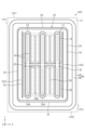
- FIG. 1 is a schematic plan view of an exemplary nitride semiconductor device according to one embodiment.
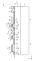
- FIG. 2 is a schematic cross-sectional view of the nitride semiconductor device taken along line F2-F2 in FIG.
- FIG. 3 is a schematic cross-sectional view showing an exemplary manufacturing process of an active region nitride semiconductor device.
- FIG. 4 is a schematic cross-sectional view showing a manufacturing process subsequent to the process shown in FIG. 3.
- FIG. 5 is a schematic cross-sectional view showing a manufacturing process following the process shown in FIG. 4.
- FIG. 6 is a schematic cross-sectional view showing a manufacturing process subsequent to the process shown in FIG.
- FIG. 7 is a schematic cross-sectional view showing a manufacturing process following the process shown in FIG. 6.
- FIG. 8 is a schematic cross-sectional view showing a manufacturing process subsequent to the process shown in FIG. 7.
- FIG. 9 is a schematic cross-sectional view showing a manufacturing process following the process shown in FIG. 8.
- FIG. 10 is a schematic cross-sectional view showing a manufacturing process subsequent to the process shown in FIG.
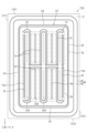
- FIG. 11 is a schematic plan view of an exemplary nitride semiconductor device according to the first modification.
- FIG. 12 is a schematic plan view of an exemplary nitride semiconductor device according to a second modification example.
- FIG. 13 is a schematic plan view of an exemplary nitride semiconductor device according to a third modification.
- FIG. 14 is a schematic cross-sectional view of the nitride semiconductor device taken along line F14-F14 in FIG. 13.
- FIG. 15 is a schematic plan view of an exemplary nitride semiconductor device according to a fourth modification.
- FIG. 16 is a schematic plan view of an exemplary nitride semiconductor device according to a fifth modification.
- FIG. 17 is a schematic cross-sectional view of the nitride semiconductor device taken along line F17-F17 in FIG. 16.
- FIG. 18 is a schematic plan view of an exemplary nitride semiconductor device according to a sixth modification.
- FIG. 19 is a schematic plan view of an exemplary nitride semiconductor device according to a seventh modification.
- FIG. 20 is a schematic cross-sectional view of an exemplary nitride semiconductor device according to an eighth modification.
- FIG. 21 is a schematic cross-sectional view of an exemplary nitride semiconductor device according to a ninth modification.
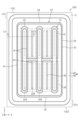
- FIG. 1 is a schematic plan view of an exemplary nitride semiconductor device 10 according to one embodiment.
- Nitride semiconductor device 10 includes a nitride semiconductor layer 12, a gate layer 14 formed on nitride semiconductor layer 12, and a gate electrode 16 formed on gate layer 14.
- the Z-axis direction of the mutually perpendicular XYZ axes shown in FIG. 1 is a direction perpendicular to the surface of the nitride semiconductor layer 12 on which a device is formed.
- the term "planar view” used in this specification refers to viewing the nitride semiconductor device 10 from above along the Z-axis direction, unless explicitly stated otherwise.
- the upper surface of the nitride semiconductor layer 12 can include two sides 12X1 and 12X2 extending along the X-axis direction and two sides 12Y1 and 12Y2 extending along the Y-axis direction.
- the area defined by the four sides 12X1, 12X2, 12Y1, and 12Y2 of the nitride semiconductor layer 12 may correspond to one chip (die). Further details of the nitride semiconductor layer 12 will be described later with reference to FIG.
- the gate layer 14 is made of a nitride semiconductor containing acceptor type impurities.
- the gate layer 14 may be a gallium nitride layer (p-type GaN layer) doped with acceptor type impurities.
- the acceptor type impurity can include at least one of zinc (Zn), magnesium (Mg), and carbon (C).
- the maximum concentration of acceptor type impurities in the gate layer 14 may be, for example, 7 ⁇ 10 18 cm ⁇ 3 or more and 1 ⁇ 10 20 cm ⁇ 3 or less.
- the gate layer 14 includes a plurality of main gate portions 18 that extend in the Y-axis direction (first direction) and are arranged in the X-axis direction (second direction) in plan view. Note that in this specification, the Y-axis direction is also referred to as a first direction, and the X-axis direction is also referred to as a second direction. In the example of FIG. 1, the gate layer 14 includes four main gate parts 18. The number of main gate sections 18 can be arbitrarily determined depending on the desired layout of the nitride semiconductor device 10 or the area (chip area) of the nitride semiconductor layer 12.
- the gate layer 14 may further include a plurality of gate connection parts 20 that interconnect the plurality of main gate parts 18.
- three gate connecting parts 20 connect two main gate parts 18.
- the number of gate connecting portions 20 can be arbitrarily determined depending on the desired layout of nitride semiconductor device 10 or the area (chip area) of nitride semiconductor layer 12.
- the gate connecting part 20 can be configured to connect two main gate parts 18 spaced apart in the X-axis direction.
- the gate electrode 16 may be composed of one or more metal layers.
- gate electrode 16 may be comprised of a titanium nitride (TiN) layer.
- the gate electrode 16 may include a first metal layer made of Ti and a second metal layer made of TiN provided on the first metal layer.
- the gate electrode 16 can form a Schottky junction with the gate layer 14.
- the gate electrode 16 may be formed in a region smaller than the gate layer 14 in plan view.
- the nitride semiconductor device 10 may further include a dummy pattern 22 formed on the nitride semiconductor layer 12.
- the dummy pattern 22 is formed in a closed ring shape so as to surround the gate layer 14 in plan view.
- the dummy pattern 22 may extend generally along the four sides 12X1, 12X2, 12Y1, and 12Y2 of the nitride semiconductor layer 12 in plan view.
- the dummy pattern 22 is formed on the nitride semiconductor layer 12 and includes a first dummy part 24 and a second dummy part 26 that extend in the Y-axis direction in plan view.
- the first dummy section 24 and the second dummy section 26 are made of a nitride semiconductor containing acceptor type impurities.
- the dummy pattern 22 may further include a third dummy part 28 and a fourth dummy part 30 that are formed on the nitride semiconductor layer 12 and extend in the X-axis direction in plan view.
- the third dummy section 28 and the fourth dummy section 30 are made of a nitride semiconductor containing acceptor type impurities.
- the first dummy part 24, the second dummy part 26, the third dummy part 28, and the fourth dummy part 30 constitute at least a part of the ring-shaped dummy pattern 22 in plan view. There is.
- the nitride semiconductor device 10 may further include a dummy electrode 32 formed on the dummy pattern 22.
- the dummy electrode 32 may be made of the same metal layer as the gate electrode 16.
- the dummy electrode 32 may be formed in an area smaller than the dummy pattern 22 in plan view.
- the dummy electrode 32 may be electrically floating.
- the nitride semiconductor device 10 further includes a passivation layer 34 (see FIG. 2) having a plurality of source openings 34A and a plurality of drain openings 34B.
- the passivation layer 34 is shown to be transparent so that the layers below the passivation layer 34 are visible, but the plurality of source openings 34A and the plurality of drain openings 34B are depicted in dashed lines.
- the passivation layer 34 covers the gate layer 14, the gate electrode 16, the dummy pattern 22 (the first dummy part 24, the second dummy part 26, the third dummy part 28, and the fourth dummy part 30), and the dummy electrode 32. good.
- source openings 34A and four drain openings 34B are formed in the passivation layer 34.
- Two source openings 34A spaced apart from each other are lined up in the Y-axis direction.
- two drain openings 34B spaced apart from each other are lined up in a line in the Y-axis direction.
- Source openings 34A and drain openings 34B are arranged alternately in the X-axis direction.
- the number of source openings 34A and the number of drain openings 34B can be arbitrarily determined depending on the desired layout of nitride semiconductor device 10 or the area (chip area) of nitride semiconductor layer 12.
- the number of source openings 34A and drain openings 34B can be determined depending on, for example, the number of main gate sections 18.
- Each main gate section 18 is arranged between one of the plurality of source openings 34A and one of the plurality of drain openings 34B.
- Each gate connection part 20 is spaced apart from at least one of the plurality of drain openings 34B in the Y-axis direction. Some of the plurality of gate coupling parts 20 are arranged between two drain openings 34B aligned in a row in the Y-axis direction.
- the gate layer 14, the plurality of source openings 34A, and the plurality of drain openings 34B are arranged between the first dummy part 24 and the second dummy part 26, which are separated in the X-axis direction in plan view.
- the gate layer 14, the plurality of source openings 34A, and the plurality of drain openings 34B are arranged between the third dummy part 28 and the fourth dummy part 30, which are separated in the Y-axis direction in plan view. .
- the nitride semiconductor device 10 includes a source electrode 36 in contact with the nitride semiconductor layer 12 through a plurality of source openings 34A, and a drain electrode 38 in contact with the nitride semiconductor layer 12 through a plurality of drain openings 34B. further including.
- the source electrode 36 is drawn with a chain double-dashed line, but is shown to be transparent so that the layer below the source electrode 36 can be seen.
- the source electrode 36 and the drain electrode 38 can be constituted by one or more metal layers (eg, a combination of a Ti layer, a TiN layer, an Al layer, an AlSiCu layer, an AlCu layer, etc.).
- the source electrode 36 and the drain electrode 38 are arranged between the first dummy part 24 and the second dummy part 26, which are separated in the X-axis direction in plan view. Similarly, the source electrode 36 and the drain electrode 38 are arranged between the third dummy part 28 and the fourth dummy part 30, which are separated in the Y-axis direction in plan view.
- Source electrode 36 can be arranged to partially cover gate layer 14 and gate electrode 16. Details of the source electrode 36 will be described later with reference to FIG. 2.
- Drain electrode 38 can be arranged to cover drain opening 34B. The drain electrode 38 is arranged so as not to overlap the gate layer 14 and the gate electrode 16 in plan view.
- the nitride semiconductor device 10 may further include a guard ring 40 formed on the nitride semiconductor layer.
- the guard ring 40 is formed to surround the dummy pattern 22 in plan view.
- Guard ring 40 may include a guard ring layer 42 formed on nitride semiconductor layer 12 and a guard ring electrode 44 formed on guard ring layer 42.
- the guard ring layer 42 may be made of a nitride semiconductor containing acceptor type impurities.
- the guard ring electrode 44 may be made of the same metal layer as the source electrode 36 and the drain electrode 38. Guard ring electrode 44 may be electrically connected to source electrode 36 .
- FIG. 2 is a schematic cross-sectional view of the nitride semiconductor device 10 taken along line F2-F2 in FIG.
- Nitride semiconductor device 10 may include a semiconductor substrate 50, a buffer layer 52 formed on semiconductor substrate 50, and the above-described nitride semiconductor layer 12.
- the nitride semiconductor layer 12 may include an electron transit layer 54 formed on the buffer layer 52 and an electron supply layer 56 formed on the electron transit layer 54.
- Semiconductor substrate 50 may be formed of silicon (Si), silicon carbide (SiC), GaN, sapphire, or other substrate material.
- semiconductor substrate 50 may be a Si substrate.
- the thickness of the semiconductor substrate 50 can be, for example, 200 ⁇ m or more and 1500 ⁇ m or less.
- the buffer layer 52 can be located between the semiconductor substrate 50 and the electron transit layer 54.
- buffer layer 52 can be comprised of any material that can facilitate epitaxial growth of electron transport layer 54.
- Buffer layer 52 may include one or more nitride semiconductor layers.
- buffer layer 52 can include at least one of an aluminum nitride (AlN) layer, an aluminum gallium nitride (AlGaN) layer, and a graded AlGaN layer with a different aluminum (Al) composition.
- the buffer layer 52 may be formed by a single AlN layer, a single AlGaN layer, a layer having an AlGaN/GaN superlattice structure, a layer having an AlN/AlGaN superlattice structure, or a layer having an AlN/GaN superlattice structure. may be configured.
- the buffer layer 52 may include a first buffer layer that is an AlN layer formed on the semiconductor substrate 50 and a second buffer layer that is an AlGaN layer formed on the AlN layer.
- the first buffer layer may be, for example, an AlN layer with a thickness of 200 nm
- the second buffer layer may be formed by laminating multiple graded AlGaN layers, for example, with a thickness of 300 nm. You can leave it there.
- impurities may be introduced into a part of the buffer layer 52 to make the buffer layer 52 semi-insulating.
- the impurity is, for example, carbon (C) or iron (Fe), and the concentration of the impurity can be, for example, 4 ⁇ 10 16 cm ⁇ 3 or more.
- the electron transit layer 54 is made of a nitride semiconductor.
- the electron transit layer 54 may be, for example, a GaN layer.
- the thickness of the electron transit layer 54 can be, for example, 0.5 ⁇ m or more and 2 ⁇ m or less.
- impurities may be introduced into a part of the electron transit layer 54 to make the region other than the surface layer of the electron transit layer 54 semi-insulating.
- the impurity may be, for example, C.
- the impurity concentration in the electron transit layer 54 can be, for example, 4 ⁇ 10 16 cm ⁇ 3 or more.
- the electron transit layer 54 can include a plurality of GaN layers having different impurity concentrations, for example, a C-doped GaN layer and a non-doped GaN layer.
- the C-doped GaN layer may be formed on the buffer layer 52.
- the C-doped GaN layer can have a thickness of 0.3 ⁇ m or more and 2 ⁇ m or less.
- the C concentration in the C-doped GaN layer can be set to 5 ⁇ 10 17 cm ⁇ 3 or more and 9 ⁇ 10 19 cm ⁇ 3 or less.
- the non-doped GaN layer is formed on the C-doped GaN layer and can have a thickness of 0.05 ⁇ m or more and 0.4 ⁇ m or less.
- the non-doped GaN layer is in contact with the electron supply layer 56.
- electron transit layer 54 may include a 0.4 ⁇ m thick C-doped GaN layer and a 0.4 ⁇ m thick undoped GaN layer.
- the C concentration in the C-doped GaN layer may be about 2 ⁇ 10 19 cm ⁇ 3 .
- the electron supply layer 56 is made of a nitride semiconductor having a larger band gap than the electron transit layer 54.
- the electron supply layer 56 may be, for example, an AlGaN layer.
- the electron supply layer 56 is composed of Al x Ga 1-x N, where x satisfies 0.1 ⁇ x ⁇ 0.4, more preferably 0.1 ⁇ x ⁇ 0.3.
- the electron supply layer 56 may have a thickness of 5 nm or more and 20 nm or less. In one example, electron supply layer 56 may have a thickness of 8 nm or more.
- the electron transport layer 54 and the electron supply layer 56 are made of nitride semiconductors having different lattice constants. Therefore, the nitride semiconductor (eg, GaN) forming the electron transit layer 54 and the nitride semiconductor (eg, AlGaN) forming the electron supply layer 56 form a lattice mismatched heterojunction. Due to the spontaneous polarization of the electron transit layer 54 and the electron supply layer 56 and the piezo polarization caused by crystal strain near the heterojunction interface, the energy level of the conduction band of the electron transit layer 54 near the heterojunction interface is lower than the Fermi level. It gets lower.
- the nitride semiconductor eg, GaN
- the nitride semiconductor eg, AlGaN
- two-dimensional electron gas (2DEG) spreads within the electron transit layer 54 at a position close to the heterojunction interface between the electron transit layer 54 and the electron supply layer 56 (for example, within a range of several nm from the interface). There is. Note that by increasing at least one of the Al composition and the thickness of the electron supply layer 56, the sheet carrier density of 2DEG generated in the electron transit layer 54 can be increased.
- gate layer 14 is formed on electron supply layer 56.
- the gate layer 14 may be a GaN layer having a smaller bandgap than the electron supply layer 56, which is, for example, an AlGaN layer.
- FIG. 2 a cross section of the main gate portion 18 of the gate layer 14 is shown.
- the main gate section 18 is located between the source opening 34A and the drain opening 34B. More specifically, the main gate portion 18 may be located between the source opening 34A and the drain opening 34B, and closer to the source opening 34A than the drain opening 34B.
- the source electrode 36 is in contact with the electron supply layer 56 via the source opening 34A.
- the drain electrode 38 is in contact with the electron supply layer 56 via the drain opening 34B.
- the main gate portion 18 includes a bottom surface 18A in contact with the nitride semiconductor layer 12 (electron supply layer 56) and an upper surface 18B on which the gate electrode 16 is formed.
- the main gate portion 18 includes a gate ridge portion 58 including the upper surface 18B, and a source side extension portion 60 and a drain side extension portion 62 having a thickness smaller than that of the gate ridge portion 58. It's okay to be there.
- the source side extension part 60 and the drain side extension part 62 extend outward from the gate ridge part 58 in plan view.
- the gate ridge portion 58 is depicted as the main gate portion 18, and the source side extension portion 60 and the drain side extension portion 62 are omitted.
- the source side extension portion 60 extends from the gate ridge portion 58 toward the source opening 34A in plan view. Note that the source opening 34A referred to here refers to the one closest to the gate ridge portion 58 among the plurality of source openings 34A. The source side extension portion 60 does not reach the source opening 34A. The source side extension portion 60 is separated from the source electrode 36 by the passivation layer 34 .
- the drain side extension portion 62 extends from the gate ridge portion 58 toward the drain opening 34B in plan view. Note that the drain opening 34B referred to here refers to the one closest to the gate ridge portion 58 among the plurality of drain openings 34B. The drain side extension portion 62 does not reach the drain opening 34B. The drain side extension portion 62 is separated from the drain electrode 38 by the passivation layer 34 .
- the gate ridge portion 58 is located between the source side extending portion 60 and the drain side extending portion 62, and is formed integrally with the source side extending portion 60 and the drain side extending portion 62. Due to the existence of the source-side extension portion 60 and the drain-side extension portion 62, the bottom surface 18A of the main gate portion 18 has a larger area than the top surface 18B. In the example shown in FIG. 2, the drain side extension part 62 extends longer toward the outside of the gate ridge part 58 in plan view than the source side extension part 60. That is, the drain side extension part 62 has a larger dimension in the X-axis direction than the source side extension part 60.
- the source side extension part 60 and the drain side extension part 62 may have the same dimensions in the X-axis direction.
- the source side extension portion 60 may have a dimension of, for example, 0.2 ⁇ m or more and 0.3 ⁇ m or less in the X-axis direction.
- the drain side extension portion 62 may have a dimension of, for example, 0.2 ⁇ m or more and 0.6 ⁇ m or less in the X-axis direction.
- the gate ridge portion 58 corresponds to a relatively thick portion of the main gate portion 18.
- the gate ridge portion 58 may have a thickness of, for example, 80 nm or more and 150 nm or less.
- the thickness of the main gate portion 18, particularly the gate ridge portion 58, can be determined by considering parameters including the gate threshold voltage.
- the main gate portion 18 (gate ridge portion 58) may have a thickness greater than 110 nm.
- Each of the source side extension part 60 and the drain side extension part 62 has a thickness smaller than the thickness of the gate ridge part 58.
- each of the source-side extension portion 60 and the drain-side extension portion 62 may have a thickness that is less than or equal to half the thickness of the gate ridge portion 58.
- Each of the source-side extension portion 60 and the drain-side extension portion 62 may include a flat portion having a substantially constant thickness. As shown in FIG. 2, each of the source side extension part 60 and the drain side extension part 62 may further include an inclined part having a thickness that gradually decreases as the distance from the gate ridge part 58 increases. The sloped portion is formed between the gate ridge portion 58 and the flat portion. In one example, the flat portions of the source-side extension portion 60 and the drain-side extension portion 62 may have a thickness of 5 nm or more and 25 nm or less. Note that in this specification, "substantially constant thickness” refers to a thickness within a range of manufacturing variations (for example, 20%).
- the gate electrode 16 is formed on the gate layer 14. As shown in FIG. 2, the gate electrode 16 is formed on the gate ridge portion 58 including the upper surface 18B of the main gate portion 18. As shown in FIG.
- the thickness of the gate electrode 16 may be, for example, 50 nm or more and 200 nm or less.
- the source electrode 36 may include a source contact plug portion 36A filled in the source opening 34A and a source field plate portion 36B covering the passivation layer 34.
- the source field plate section 36B may be continuous with the source contact plug section 36A. In this case, the source field plate section 36B is formed integrally with the source contact plug section 36A.
- the source field plate portion 36B includes an end portion 36C located between the drain opening 34B and the main gate portion 18 in plan view. The source field plate portion 36B extends along the surface of the passivation layer 34 from the source contact plug portion 36A to the end portion 36C toward the drain electrode 38, but is spaced apart from the drain electrode 38.
- Source field plate portion 36B extends along the non-flat surface of passivation layer 34, and therefore has a similarly non-flat surface.
- the source field plate portion 36B plays a role of alleviating electric field concentration near the end of the gate electrode 16 when a drain voltage is applied to the drain electrode 38 in a zero bias state where no gate voltage is applied to the gate electrode 16. is fulfilled.
- At least a portion of the source electrode 36 is filled in the source opening 34A, so it can make ohmic contact with the 2DEG directly below the electron supply layer 56 via the source opening 34A.
- the drain electrode 38 is filled in the drain opening 34B, it can make ohmic contact with the 2DEG directly below the electron supply layer 56 via the drain opening 34B.
- the nitride semiconductor device 10 may include an active region 64 that contributes to transistor operation and an inactive region 66 that does not contribute to transistor operation.
- an active region 64 that contributes to transistor operation
- an inactive region 66 that does not contribute to transistor operation.
- a region extending in the X-axis direction from the source opening 34A (source contact plug portion 36A) to the drain opening 34B (drain electrode 38) generally corresponds to the active region 64.
- the main gate section 18 is made of a nitride semiconductor (for example, p-type GaN) containing acceptor type impurities, the active region 64 including the main gate section 18 is capable of normally-off operation. It can function as a HEMT.
- the nitride semiconductor device 10 includes a plurality of source openings 34A and a plurality of drain openings 34B arranged alternately in the X-axis direction, and each main gate section 18 has a plurality of is disposed between one of the source openings 34A and one of the plurality of drain openings 34B. Therefore, the active areas 64 shown in FIG. 2 may be repeated with every other active area being reversed in the X-axis direction. In the case of the example in FIG. 1, a region extending in the X-axis direction from the source opening 34A closest to the first dummy section 24 to the source opening 34A closest to the second dummy section 26 may correspond to the active region 64. Further, the active region 64 may extend in the same range as the source opening 34A or the drain opening 34B in the Y-axis direction.
- a first dummy portion 24, which is a part of the dummy pattern 22, and a guard ring 40 are formed on the electron supply layer 56.
- the first dummy portion 24 is located between the guard ring 40 and the source opening 34A in the X-axis direction.
- the second dummy portion 26 can have the same cross-sectional structure as the first dummy portion 24 shown in FIG. 2. It should be noted that the description regarding the first dummy section 24 is equally applicable to the second dummy section 26.
- the first dummy portion 24 is made of a nitride semiconductor containing acceptor type impurities.
- the first dummy portion 24 includes a bottom surface 24A in contact with the nitride semiconductor layer 12 (electron supply layer 56), and an upper surface 24B on the opposite side of the bottom surface 24A.
- the first dummy portion 24 includes a dummy ridge portion 68 including the upper surface 24B, and an outer extending portion 70 and an inner extending portion 72 having a thickness smaller than that of the dummy ridge portion 68. It's okay to stay. Note that in the plan view shown in FIG.
- a dummy ridge portion 68 is depicted as the first dummy portion 24, and the outer extending portion 70 and the inner extending portion 72 are omitted.
- the dummy electrode 32 is formed on the upper surface 24B of the first dummy part 24.
- the first dummy part 24 and the dummy electrode 32 formed on the first dummy part 24 are covered with a passivation layer 34.
- the outer extending portion 70 extends from the dummy ridge portion 68 toward the guard ring 40 in plan view.
- the dummy pattern 22 since the dummy pattern 22 is formed in a ring shape in a plan view, the dummy pattern 22 separates the inner region surrounded by the dummy pattern 22 from the outer region of the dummy pattern 22. There is.
- the outer extending portion 70 exists in a region outside the dummy pattern 22 . In the example of FIG. 2, the outer extension 70 does not reach the guard ring 40. Outer extension 70 is spaced from guard ring 40 by passivation layer 34 .
- the inner extending portion 72 extends from the dummy ridge portion 68 toward the gate layer 14 (main gate portion 18) in plan view.
- the inner extending portion 72 exists in an inner region surrounded by the dummy pattern 22 .
- the inner extension portion 72 does not reach the source opening 34A.
- Inner extension 72 is spaced from source electrode 36 by passivation layer 34 .
- the dummy ridge portion 68 of the first dummy portion 24 is located between the outer extending portion 70 and the inner extending portion 72, and is formed integrally with the outer extending portion 70 and the inner extending portion 72. Due to the presence of the outer extending portion 70 and the inner extending portion 72, the bottom surface 24A of the first dummy portion 24 has a larger area than the top surface 24B. As shown in FIG. 2, the outer extending portion 70 and the inner extending portion 72 may have the same dimensions in the X-axis direction. The outer extending portion 70 and the inner extending portion 72 may have a dimension of, for example, 0.2 ⁇ m or more and 0.3 ⁇ m or less in the X-axis direction.
- the dummy ridge portion 68 corresponds to a relatively thick portion of the first dummy portion 24.
- the dummy ridge portion 68 may have a thickness of 80 nm or more and 150 nm or less.
- Each of the outer extension portion 70 and the inner extension portion 72 has a thickness smaller than the thickness of the dummy ridge portion 68. In one example, each of the outer extension portion 70 and the inner extension portion 72 may have a thickness that is less than or equal to half the thickness of the dummy ridge portion 68.
- Each of the outer extension portion 70 and the inner extension portion 72 may include a flat portion having a substantially constant thickness.
- Each of the outer extension portion 70 and the inner extension portion 72 may further include an inclined portion having a thickness that gradually decreases as the distance from the dummy ridge portion 68 increases, as shown in FIG. 2 .
- the sloped portion is formed between the dummy ridge portion 68 and the flat portion.
- the flat portions of the outer extending portion 70 and the inner extending portion 72 may have a thickness of 5 nm or more and 25 nm or less.
- the first dummy portion 24 is formed by the same manufacturing process as the main gate portion 18 (described later with reference to FIGS. 3 to 10). Therefore, the first dummy part 24 can have a thickness comparable to that of the main gate part 18 within the range of manufacturing variations.
- the dimension (design dimension) of the dummy ridge portion 68 in the X-axis direction may be the same as the dimension (design dimension) of the gate ridge portion 58 in the X-axis direction.
- the dimensions in the X-axis direction (design dimensions) of the outer extension part 70 and the inner extension part 72 of the first dummy part 24 are the dimensions (design dimensions) in the X-axis direction of the source side extension part 60 and the drain side extension part 62, respectively.
- the dimensions in the X-axis direction of the outer extending portion 70 and the inner extending portion 72 of the first dummy portion 24 may be the same.
- the dimensions of the outer extending portion 70 and the inner extending portion 72 in the X-axis direction may be, for example, the same as the dimension of the drain-side extending portion 62 in the X-axis direction.
- the source opening 34A located between the gate layer 14 and the first dummy part 24 may be arranged at an equal distance from both the gate layer 14 (main gate part 18) and the first dummy part 24 in plan view.
- the guard ring layer 42 is made of a nitride semiconductor containing acceptor type impurities.
- Guard ring layer 42 includes a bottom surface 42A in contact with nitride semiconductor layer 12 (electron supply layer 56), and an upper surface 24B on which guard ring electrode 44 is formed.
- the guard ring layer 42 includes a guard ring ridge portion 74 including the upper surface 42B, and an outer extending portion 76 and an inner extending portion 78 having a thickness smaller than the guard ring ridge portion 74. It's okay to be there. Note that in the plan view shown in FIG.
- a guard ring ridge portion 74 is depicted as the guard ring layer 42, and the outer extending portion 76 and the inner extending portion 78 are omitted.
- the guard ring electrode 44 is formed on the upper surface 42B of the guard ring layer 42.
- the guard ring layer 42 and the guard ring electrode 44 formed on the guard ring layer 42 are covered with a passivation layer 34.
- the outer extending portion 76 extends from the guard ring ridge portion 74 toward the outer side of the guard ring 40 in plan view. As shown in FIG. 1, the guard ring 40 is formed into a ring shape in plan view, so the guard ring 40 has an inner region surrounded by the guard ring 40 and an outer region of the guard ring 40. Separated. The outer extension 76 is present in the outer region of the guard ring 40 .
- the inner extending portion 78 extends from the guard ring ridge portion 74 toward the inner side of the guard ring 40 in plan view.
- the inner extending portion 78 exists in an inner region surrounded by the guard ring 40 . In the example of FIG. 2, the inner extending portion 78 does not reach the first dummy portion 24.
- the inner extension portion 78 is separated from the first dummy portion 24 by the passivation layer 34 .
- the guard ring ridge portion 74 of the guard ring layer 42 is located between the outer extending portion 76 and the inner extending portion 78, and is formed integrally with the outer extending portion 76 and the inner extending portion 78. Due to the presence of the outer extension portion 76 and the inner extension portion 78, the bottom surface 42A of the guard ring layer 42 has a larger area than the top surface 42B. As shown in FIG. 2, the outer extending portion 76 and the inner extending portion 78 may have the same length in the X-axis direction. The outer extending portion 76 and the inner extending portion 78 may have a length of, for example, 0.2 ⁇ m or more and 0.3 ⁇ m or less in the X-axis direction.
- the guard ring ridge portion 74 corresponds to a relatively thick portion of the guard ring layer 42, and can have a thickness of 80 nm or more and 150 nm or less.
- Each of the outer extension 76 and the inner extension 78 has a thickness that is less than the thickness of the guard ring ridge 74.
- each of the outer extensions 76 and the inner extensions 78 may have a thickness that is less than or equal to half the thickness of the guard ring ridge 74.
- Each of the outer extension portion 76 and the inner extension portion 78 may include a flat portion having a substantially constant thickness.
- Each of the outer extension portion 76 and the inner extension portion 78 may further include a sloped portion having a thickness that gradually decreases as the distance from the guard ring ridge portion 74 increases, as shown in FIG. 2 .
- the sloped portion is formed between the guard ring ridge portion 74 and the flat portion.
- the flat portions of the outer extending portion 76 and the inner extending portion 78 may have a thickness of 5 nm or more and 25 nm or less.
- the guard ring layer 42 is formed by the same manufacturing process as the main gate portion 18 (described later with reference to FIGS. 3 to 10). Therefore, the guard ring layer 42 may have a thickness comparable to that of the main gate portion 18 within the range of manufacturing variations.
- the width of the guard ring ridge portion 74 (the dimension in the X-axis direction in FIG. 2) is larger than the dimension of any of the source opening 34A, the drain opening 34B, and the gate ridge portion 58 in the X-axis direction.
- the dimensions in the X-axis direction of the outer extending portion 76 and the inner extending portion 78 of the guard ring layer 42 may be the same or different.
- the first dummy portion 24 and guard ring layer 42 described above do not directly contribute to the transistor operation of the nitride semiconductor device 10.
- a region where the dummy pattern 22 including the first dummy portion 24 and the guard ring 40 including the guard ring layer 42 are formed is included in the inactive region 66 .
- FIGS. 3 to 10 are schematic cross-sectional views showing exemplary manufacturing steps of the nitride semiconductor device 10. Note that, in order to facilitate understanding, in FIGS. 3 to 10, the same reference numerals may be given to the same components as those in FIG. 2.
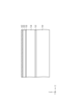
- the method for manufacturing the nitride semiconductor device 10 includes forming a buffer layer 52, an electron transit layer 54, an electron supply layer 56, a gallium nitride (GaN) layer 80, on a semiconductor substrate 50, which is a Si substrate, for example. This includes sequentially forming a metal layer 82.
- the buffer layer 52, the electron transit layer 54, the electron supply layer 56, and the GaN layer 80 can be epitaxially grown using a metal organic chemical vapor deposition (MOCVD) method.
- MOCVD metal organic chemical vapor deposition
- the metal layer 82 can be formed using a sputtering method.
- the buffer layer 52 may be a multilayer buffer layer.
- the multilayer buffer layer may include an AlN layer (first buffer layer) formed on the semiconductor substrate 50 and a graded AlGaN layer (second buffer layer) formed on the AlN layer.
- the graded AlGaN layer can be formed, for example, by stacking three AlGaN layers with Al compositions of 75%, 50%, and 25% in order from the side closest to the AlN layer.
- the electron transit layer 54 formed on the buffer layer 52 may be a GaN layer.
- the electron supply layer 56 formed on the electron transit layer 54 may be an AlGaN layer. Therefore, the electron supply layer 56 is made of a nitride semiconductor having a larger band gap than the electron transit layer 54.
- the GaN layer 80 formed on the electron supply layer 56 may contain magnesium as an acceptor type impurity.
- the GaN layer 80 containing acceptor type impurities can be formed.
- the amount of magnesium doped into the GaN layer 80 can be adjusted by, for example, controlling the flow rate of a doping gas (for example, biscyclopentadienylmagnesium (Cp 2 Mg)) introduced into the growth chamber, the growth temperature, etc. can do.
- a doping gas for example, biscyclopentadienylmagnesium (Cp 2 Mg)
- the GaN layer 80 may contain magnesium as an impurity at a concentration of 1 ⁇ 10 18 cm ⁇ 3 or more and less than 1 ⁇ 10 20 cm ⁇ 3 .
- the metal layer 82 can be formed on the GaN layer 80 by, for example, sputtering.
- the metal layer 82 may be a TiN layer, in one example.
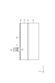
- FIG. 4 is a schematic cross-sectional view showing a manufacturing process subsequent to the process shown in FIG. 3.
- the method for manufacturing nitride semiconductor device 10 further includes selectively removing metal layer 82 by lithography and etching to form gate electrode 16.
- a mask 84 is formed on the portion of the metal layer 82 that is to be used as the gate electrode 16.
- the mask 84 can be formed, for example, by exposing a photoresist provided on the metal layer 82.
- mask 84 may be a hard mask.
- the metal layer 82 in the area not covered by the mask 84 is removed.
- the metal layer 82 in the area covered by the mask 84 remains, and the gate electrode 16 can be formed.
- Mask 84 is removed after etching.
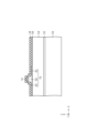
- FIG. 5 is a schematic cross-sectional view showing a manufacturing process following the process shown in FIG. 4.
- the method for manufacturing nitride semiconductor device 10 further includes selectively removing GaN layer 80 by lithography and etching to form gate ridge portion 58.
- a mask 86 is formed that covers the top and side surfaces of the gate electrode 16, and the GaN layer 80 is patterned using the mask 86.
- the GaN layer 80 located under the mask 86 remains after etching, and the gate ridge portion 58 of the main gate portion 18 shown in FIG. 2 is formed.
- the thickness of GaN layer 80 not covered by mask 86 is reduced by etching.
- the GaN layer 80 has a thickness that gradually decreases as the distance from the gate ridge part 58 increases in a region adjacent to the gate ridge part 58, but in a region beyond a predetermined distance from the gate ridge part 58, the thickness of the GaN layer 80 gradually decreases as the distance from the gate ridge part 58 increases. It may be etched to have a constant thickness.
- the etching process shown in FIG. 5 may include multiple etching steps to obtain the desired shape, as described above, or may be selected such that the etching rate is slower in the vicinity of the structures covered by mask 86.
- the etching step may include a single etching step depending on the conditions.
- the mask 86 may be a resist mask or a hard mask.
- the mask 86 may be a hard mask formed of a SiN film that can be formed conformally. Mask 86 is removed after etching.
- FIG. 6 is a schematic cross-sectional view showing a manufacturing process following the process shown in FIG. 5.
- the method for manufacturing the nitride semiconductor device 10 includes selectively removing the GaN layer 80 by lithography and etching to form a source side extension part 60 and a drain side extension part 62. Including further.
- a mask 88 is formed that covers the gate electrode 16, the gate ridge portion 58, and the portions of the GaN layer 80 corresponding to the source side extension portion 60 and the drain side extension portion 62, and then the mask 88 is used to The GaN layer 80 is then patterned.
- the main gate section 18 including the gate ridge section 58, the source side extension section 60, and the drain side extension section 62 is formed on the electron supply layer 56.
- Mask 88 is removed after etching.
- FIG. 7 is a schematic cross-sectional view showing a manufacturing process following the process shown in FIG. 6.
- the method for manufacturing nitride semiconductor device 10 further includes forming a passivation layer 34 to cover the entire exposed surfaces of electron supply layer 56, main gate section 18, and gate electrode 16.
- the passivation layer 34 may be a SiN layer formed by a low-pressure chemical vapor deposition (LPCVD) method.
- FIG. 8 is a schematic cross-sectional view showing a manufacturing process following the process shown in FIG. 7.
- the method for manufacturing nitride semiconductor device 10 further includes selectively removing passivation layer 34 by lithography and etching to form source opening 34A and drain opening 34B.
- a mask 90 is formed that covers the passivation layer 34 except for regions where the source opening 34A and the drain opening 34B are to be formed, and then the passivation layer 34 is patterned using the mask 90.
- a source opening 34A and a drain opening 34B that expose the electron supply layer 56 are formed.
- the source opening 34A and the drain opening 34B are formed such that the main gate portion 18 is located between the source opening 34A and the drain opening 34B.
- the main gate portion 18 may be located closer to the source opening 34A than the drain opening 34B.
- Mask 90 is removed after etching.
- FIG. 9 is a schematic cross-sectional view showing a manufacturing process following the process shown in FIG. 8.
- the method for manufacturing nitride semiconductor device 10 further includes forming a metal layer 92 covering passivation layer 34.
- the metal layer 92 is formed to fill the source opening 34A and the drain opening 34B and to be in contact with the electron supply layer 56 via the source opening 34A and the drain opening 34B.
- metal layer 92 may include at least one of a Ti layer, a TiN layer, an Al layer, an AlSiCu layer, and an AlCu layer.
- FIG. 10 is a schematic cross-sectional view showing a manufacturing process following the process shown in FIG. 9.
- the method for manufacturing nitride semiconductor device 10 further includes selectively removing metal layer 92 by lithography and etching to form source electrode 36 and drain electrode 38.
- a mask 94 is formed on the portions of the metal layer 92 that will become the source electrode 36 and the drain electrode 38, and then the metal layer 92 is patterned using the mask 94.
- a source electrode 36 and a drain electrode 38 are formed.
- the drain electrode 38 covers an area relatively close to the drain opening 34B, but the source electrode 36 spreads so as to cover not only the source opening 34A but also the main gate portion 18.
- An end portion 36C of the source electrode 36 (source field plate portion 36B) is located between the drain opening 34B and the main gate portion 18 in plan view.
- the dummy pattern 22 (first dummy part 24, second dummy part 26, third dummy part 28, fourth dummy part 30) and guard ring layer 42 shown in FIGS. They can be formed simultaneously by a process similar to the above process.
- the mask 86 formed on the portion of the GaN layer 80 that will become the gate ridge portion 58 is also simultaneously formed on the portion of the GaN layer 80 that will become the dummy ridge portion 68 and the guard ring ridge portion 74. It is formed. Therefore, the gate ridge portion 58, the dummy ridge portion 68, and the guard ring ridge portion 74 can be formed simultaneously by etching the GaN layer 80 using the mask 86.
- the shape of the main gate portion 18 has a large influence on the operating characteristics of the nitride semiconductor device 10 (for example, on-resistance, gate threshold voltage, maximum rating of gate-source voltage, etc.). Therefore, if the shape of the main gate portion 18 is non-uniform within the chip, gate reliability may decrease.
- the main gate portion 18 includes the source side extension portion 60 and the drain side extension portion 62
- the gate electrode 16 and The electric field strength applied to the Schottky diode formed between the main gate portion 18 and the main gate portion 18 can be reduced. Therefore, the source side extension part 60 and the drain side extension part 62 suppress the generation of gate leakage current, thereby making it possible to improve the gate breakdown voltage.
- the source side extension part 60 and the drain side extension part 62 are too thin, there is a possibility that the effect of improving the gate breakdown voltage by the source side extension part 60 and the drain side extension part 62 will be reduced. Therefore, it is important to obtain the source-side extension 60 and drain-side extension 62 with uniform shapes throughout the chip.
- the shape of the main gate portion 18 may become non-uniform. This is because some of the plurality of main gate sections 18 in the active region 64 are arranged relatively close to the inactive region 66.
- the pattern density includes a region including the main gate section 18 located at the end in the X-axis direction and a region including the main gate section 18 located at the center. It differs depending on the area. For example, in the example shown in FIG.
- the width of the guard ring ridge section 74 (in FIG. Since the dimension (in the axial direction) is larger than the dimension in the X-axis direction of the gate ridge portion 58, the pattern density is limited to the area including the main gate portion 18 located at the end in the X-axis direction and the main gate located in the center. The area including the portion 18 is different.
- the gate layer 14 including the plurality of main gate parts 18, the plurality of source openings 34A, and the plurality of drain openings 34B are spaced apart in the X-axis direction in a plan view. It is arranged between the first dummy part 24 and the second dummy part 26. Therefore, it is possible to reduce the difference in pattern density between the region including the main gate section 18 located at the end in the X-axis direction and the region including the main gate section 18 located at the center in the X-axis direction. .
- the influence of a process (for example, etching) that depends on the pattern density can be reduced, and the uniformity of the shapes of the plurality of main gate parts 18 can be improved.
- the gate reliability of the nitride semiconductor device 10 can be improved.
- the nitride semiconductor device 10 of this embodiment has the following advantages.
- (1) The gate layer 14 including the plurality of main gate parts 18, the plurality of source openings 34A, and the plurality of drain openings 34B are arranged in a first dummy part 24 and a second dummy part 26 separated in the X-axis direction in plan view. is located between. Therefore, it is possible to reduce the difference in pattern density between the region including the main gate section 18 located at the end in the X-axis direction and the region including the main gate section 18 located at the center in the X-axis direction. . As a result, the uniformity of the shapes of the plurality of main gate sections 18 can be improved.
- the nitride semiconductor device 10 further includes a guard ring 40 formed on the nitride semiconductor layer 12 so as to surround the first dummy part 24 and the second dummy part 26 in a plan view, and the guard ring 40 includes: A guard ring electrode 44 electrically connected to the source electrode 36 may be included. Thereby, the breakdown voltage of the nitride semiconductor device 10 can be improved.
- the nitride semiconductor device 10 may further include a third dummy portion 28 and a fourth dummy portion 30 that are formed on the nitride semiconductor layer 12 and extend in the X-axis direction in plan view.
- the third dummy section 28 and the fourth dummy section 30 are made of a nitride semiconductor containing acceptor type impurities.
- the gate layer 14, the plurality of source openings 34A, and the plurality of drain openings 34B are arranged between the third dummy part 28 and the fourth dummy part 30, which are separated in the Y-axis direction in plan view. As a result, the difference in pattern density between the ends and the center of the gate layer 14 in the Y-axis direction can be reduced.
- One of the plurality of source openings 34A may be arranged at an equal distance from both the gate layer 14 and the first dummy part 24 in plan view. Thereby, the uniformity of pattern density can be improved.
- Each of the plurality of main gate parts 18 has a gate ridge part 58 including the upper surface 18B, and extends from the gate ridge part 58 toward the source opening 34A in plan view, and has a thickness smaller than that of the gate ridge part 58. and a drain side extending portion 62 that extends from the gate ridge portion 58 toward the drain opening 34B in plan view and has a thickness smaller than that of the gate ridge portion 58. Since the main gate portion 18 includes the source side extension portion 60 and the drain side extension portion 62, local concentration of electric field within the main gate portion 18 can be suppressed. As a result, generation of gate leakage current is suppressed, so gate breakdown voltage can be improved.
- the guard ring layer 42 has a guard ring ridge portion 74 including the upper surface 42B, extends from the guard ring ridge portion 74 toward the outside of the guard ring 40 in plan view, and has a thickness smaller than the guard ring ridge portion 74. and an inner extending portion 78 that extends from the guard ring ridge portion 74 toward the inside of the guard ring 40 in plan view and has a thickness smaller than the guard ring ridge portion 74. It's okay to stay. Thereby, the reliability of the guard ring 40 can be improved.
- Each of the first dummy part 24 and the second dummy part 26 extends from the dummy ridge part 68 toward the guard ring 40 in plan view, and has a thickness smaller than that of the dummy ridge part 68. and an inner extending portion 72 that extends from the dummy ridge portion 68 toward the gate layer 14 (main gate portion 18) in plan view and has a thickness smaller than that of the dummy ridge portion 68. It may be included.
- the main gate portion 18 is arranged closer to the source opening 34A than the drain opening 34B. Thereby, the distance between the gate electrode 16 and the drain electrode 38 can be made relatively large, so that dielectric breakdown between the gate and the drain, which tends to be applied with a relatively large voltage, can be suppressed.
- FIG. 11 is a schematic plan view of an exemplary nitride semiconductor device 100 according to the first modification.
- the same components as those of the nitride semiconductor device 10 shown in FIG. 1 are given the same reference numerals. Further, detailed description of the same components as those of the nitride semiconductor device 10 will be omitted.
- the nitride semiconductor device 100 is different from the nitride semiconductor device 10 in that the dummy pattern 22 does not include the third dummy part 28 and the fourth dummy part 30 shown in FIG.
- the dummy pattern 22 is formed between the side 12X1 of the nitride semiconductor layer 12 and the gate layer 14 and between the side 12X2 and the gate layer 14 in a plan view. do not have. Therefore, in nitride semiconductor device 100, the chip area can be reduced compared to nitride semiconductor device 10.
- nitride semiconductor device 100 has advantages similar to advantages (1), (2), and (4) to (8) described above for nitride semiconductor device 10.
- FIG. 12 is a schematic plan view of an exemplary nitride semiconductor device 200 according to a second modification.
- the same components as those of the nitride semiconductor device 10 shown in FIG. 1 are given the same reference numerals. Further, detailed description of the same components as those of the nitride semiconductor device 10 will be omitted.
- the nitride semiconductor device 200 is different from the nitride semiconductor device 10 in that the dummy pattern 22 is not formed in a closed ring shape in plan view. As shown in FIG. 12, the first dummy part 24, the second dummy part 26, the third dummy part 28, and the fourth dummy part 30 may be spaced apart from each other. Nitride semiconductor device 200 has advantages similar to advantages (1) to (8) described above for nitride semiconductor device 10.
- FIG. 13 is a schematic plan view of an exemplary nitride semiconductor device 300 according to a third modification.
- the same components as those of the nitride semiconductor device 10 shown in FIG. 1 are given the same reference numerals. Further, detailed description of the same components as those of the nitride semiconductor device 10 will be omitted.
- the nitride semiconductor device 300 is different from the nitride semiconductor device 10 in that it further includes one or more fifth dummy parts 302 and one or more sixth dummy parts 304.
- One or more fifth dummy parts 302 and one or more sixth dummy parts 304 are formed on the nitride semiconductor layer 12 and extend in the Y-axis direction in plan view.
- One or more fifth dummy parts 302 can be arranged between the first dummy part 24 and the gate layer 14 in plan view.
- one or more sixth dummy parts 304 can be arranged between the second dummy part 26 and the gate layer 14 in plan view. In the example shown in FIG.
- nitride semiconductor device 300 includes one fifth dummy section 302 and one sixth dummy section 304.
- the nitride semiconductor device 300 may include a plurality of fifth dummy parts 302 and a plurality of sixth dummy parts 304.
- the plurality of fifth dummy parts 302 may be spaced apart from each other in the X-axis direction.
- the plurality of sixth dummy parts 304 may be spaced apart from each other in the X-axis direction.
- the one or more fifth dummy parts 302 and the one or more sixth dummy parts 304 are made of a nitride semiconductor containing acceptor type impurities.
- the dummy electrode 32 may also be formed on one or more fifth dummy parts 302 and one or more sixth dummy parts 304.
- FIG. 14 is a schematic cross-sectional view of the nitride semiconductor device 300 taken along line F14-F14 in FIG. 13.
- a fifth dummy portion 302 is formed on the electron supply layer 56.
- the fifth dummy section 302 is located between the first dummy section 24 and the source opening 34A.
- the sixth dummy portion 304 can have the same cross-sectional structure as the fifth dummy portion 302 shown in FIG. 14. It should be noted that the description regarding the fifth dummy section 302 is equally applicable to the sixth dummy section 304.
- the fifth dummy portion 302 is made of a nitride semiconductor containing acceptor type impurities.
- the fifth dummy portion 302 includes a bottom surface 302A in contact with the nitride semiconductor layer 12 (electron supply layer 56), and a top surface 302B on the opposite side of the bottom surface 302A.
- the fifth dummy portion 302 includes a dummy ridge portion 306 including an upper surface 302B, and an outer extending portion 308 and an inner extending portion 310 having a thickness smaller than that of the dummy ridge portion 306. It's okay to stay. Note that in the plan view shown in FIG.
- a dummy ridge portion 306 is depicted as the fifth dummy portion 302, and the outer extending portion 308 and the inner extending portion 310 are omitted.
- the dummy electrode 32 is formed on the upper surface 302B of the fifth dummy part 302.
- the fifth dummy part 302 and the dummy electrode 32 formed on the fifth dummy part 302 are covered with a passivation layer 34.
- the outer extending portion 308 of the fifth dummy portion 302 extends from the dummy ridge portion 306 toward the first dummy portion 24 in plan view.
- the outer extending portion 308 of the fifth dummy portion 302 may be connected to the inner extending portion 72 of the first dummy portion 24 .
- the outer extension 308 of the fifth dummy portion 302 may be separated from the inner extension 72 of the first dummy portion 24 by the passivation layer 34 .
- the inner extending portion 310 of the fifth dummy portion 302 extends from the dummy ridge portion 306 toward the gate layer 14 (main gate portion 18) in plan view.
- the inner extension 310 does not reach the source opening 34A.
- Inner extension 310 is separated from source electrode 36 by passivation layer 34 .
- the dummy ridge portion 306 of the fifth dummy portion 302 is located between the outer extending portion 308 and the inner extending portion 310 and is formed integrally with the outer extending portion 308 and the inner extending portion 310.
- the dummy ridge portion 306 corresponds to a relatively thick portion of the fifth dummy portion 302.
- the dummy ridge portion 306 may have a thickness of 80 nm or more and 150 nm or less.
- Each of the outer extension portion 308 and the inner extension portion 310 has a thickness that is less than the thickness of the dummy ridge portion 306. In one example, each of the outer extensions 308 and the inner extensions 310 may have a thickness that is less than or equal to half the thickness of the dummy ridge 306.
- Each of the outer extensions 308 and the inner extensions 310 may include a flat portion having a substantially constant thickness.
- Each of the outer extension portion 308 and the inner extension portion 310 may further include an inclined portion having a thickness that gradually decreases as the distance from the dummy ridge portion 306 increases, as shown in FIG. 14 .
- the sloped portion is formed between the dummy ridge portion 306 and the flat portion.
- the flat portions of the outer extension portion 308 and the inner extension portion 310 may have a thickness of 5 nm or more and 25 nm or less, in one example.
- the fifth dummy portion 302 is formed by the same manufacturing process as the main gate portion 18 (see FIGS. 3 to 10). Therefore, the fifth dummy section 302 can have a thickness comparable to that of the main gate section 18 within the range of manufacturing variations.
- the dimension (design dimension) of the dummy ridge portion 306 in the X-axis direction may be the same as the dimension (design dimension) of the gate ridge portion 58 in the X-axis direction.
- the source opening 34A located between the gate layer 14 and the fifth dummy part 302 may be arranged at an equal distance from both the gate layer 14 (main gate part 18) and the fifth dummy part 302 in plan view.
- the one or more fifth dummy parts 302 are arranged between the first dummy part 24 and the gate layer 14 in plan view, so the guard ring 40 The distance between the gate layer 14 (main gate section 18) and the gate layer 14 can be further increased.
- one or more sixth dummy parts 304 are arranged between the second dummy part 26 and the gate layer 14 in plan view, the guard ring 40 and the gate layer 14 (main gate part 18) The distance between the two can be further increased. Therefore, in the nitride semiconductor device 300, the influence of the guard ring 40 can be further reduced, and the uniformity of the shapes of the plurality of main gate parts 18 can be improved.
- nitride semiconductor device 300 has advantages similar to advantages (1) to (8) described above for nitride semiconductor device 10.
- FIG. 15 is a schematic plan view of an exemplary nitride semiconductor device 400 according to a fourth modification.
- the same components as those of the nitride semiconductor device 10 shown in FIG. 1 are given the same reference numerals. Further, detailed description of the same components as those of the nitride semiconductor device 10 will be omitted.
- the nitride semiconductor device 400 is different from the nitride semiconductor device 10 in that it further includes a dummy pattern 402 formed on the nitride semiconductor layer 12 and having a ring shape in plan view.
- the dummy pattern 402 is surrounded by the guard ring 40 and also surrounds the dummy pattern 22. Therefore, the dummy pattern 402 passes between the first dummy part 24 and the guard ring 40 and between the second dummy part 26 and the guard ring 40 in plan view.
- the dummy pattern 402 is made of a nitride semiconductor containing acceptor type impurities.
- the dummy electrode 32 may also be formed on the dummy pattern 402.
- the dummy pattern 402 may have the same cross-sectional shape as the dummy pattern 22.
- the dummy pattern 402 passes between the first dummy part 24 and the guard ring 40 and between the second dummy part 26 and the guard ring 40 in plan view. Therefore, the distance between the guard ring 40 and the gate layer 14 (main gate section 18) can be further increased. Therefore, in the nitride semiconductor device 400, the influence of the guard ring 40 can be further reduced, and the uniformity of the shapes of the plurality of main gate sections 18 can be improved.
- nitride semiconductor device 400 has advantages similar to advantages (1) to (8) described above for nitride semiconductor device 10.
- FIG. 16 is a schematic plan view of an exemplary nitride semiconductor device 500 according to a fifth modification.
- the same components as those of nitride semiconductor device 10 shown in FIG. 1 are given the same reference numerals. Further, detailed description of the same components as those of the nitride semiconductor device 10 will be omitted.
- both of the plurality of source openings 34A and the plurality of drain openings 34B are located between the gate layer 14 and the first dummy section 24 or between the gate layer 14 and the second dummy section 26 in plan view. It is different from the nitride semiconductor device 10 in that it is not arranged in the nitride semiconductor device 10.
- Each of the plurality of source openings 34A and the plurality of drain openings 34B is arranged between two of the plurality of main gate sections 18 in plan view.
- FIG. 17 is a schematic cross-sectional view of the nitride semiconductor device 500 taken along line F17-F17 in FIG. 16.
- FIG. 17 shows two main gate sections 18 arranged near the first dummy section 24.
- the source opening 34A is arranged between the two main gate sections 18, and between the first dummy section 24 and the main gate section 18 closest to the first dummy section 24.
- Neither the source opening 34A nor the drain opening 34B is arranged in the.
- nitride semiconductor device 500 has advantages similar to advantages (1) to (8) described above for nitride semiconductor device 10.
- FIG. 18 is a schematic plan view of an exemplary nitride semiconductor device 600 according to the sixth modification.
- the same components as those of nitride semiconductor device 500 shown in FIG. 16 are given the same reference numerals. Further, detailed description of the same components as those of nitride semiconductor device 500 will be omitted.
- the nitride semiconductor device 600 is different from the nitride semiconductor device 500 in that it further includes one or more fifth dummy parts 602 and one or more sixth dummy parts 604.
- One or more fifth dummy parts 602 and one or more sixth dummy parts 604 are formed on the nitride semiconductor layer 12 and extend in the Y-axis direction in plan view.
- One or more fifth dummy parts 602 are arranged between the first dummy part 24 and the gate layer 14 in plan view.
- one or more sixth dummy parts 604 are arranged between the second dummy part 26 and the gate layer 14 in plan view.
- the one or more fifth dummy parts 602 and the one or more sixth dummy parts 604 are the same as the one or more fifth dummy parts 302 and the one or more sixth dummy parts described with reference to FIG. They may each be the same components as the section 304.
- the one or more fifth dummy parts 602 are arranged between the first dummy part 24 and the gate layer 14 in a plan view, so that the guard ring 40 The distance between the main gate section 18 and the main gate section 18 can be further increased.
- one or more sixth dummy parts 604 are arranged between the second dummy part 26 and the gate layer 14 in plan view, the distance between the guard ring 40 and the main gate part 18 can be further separated. Therefore, in the nitride semiconductor device 600, the influence of the guard ring 40 can be further reduced, and the uniformity of the shapes of the plurality of main gate parts 18 can be improved.
- nitride semiconductor device 600 has advantages similar to advantages (1) to (8) described above for nitride semiconductor device 10.
- FIG. 19 is a schematic plan view of an exemplary nitride semiconductor device 700 according to a seventh modification.
- the same components as those of nitride semiconductor device 500 shown in FIG. 16 are given the same reference numerals. Further, detailed description of the same components as those of nitride semiconductor device 500 will be omitted.
- the nitride semiconductor device 700 has a layout obtained by separating the two main gate portions 18 at both ends from the gate layer 14 in the layout of the nitride semiconductor device 500 shown in FIG. Two parts separated from the gate layer 14 can function as a first dummy part 702 and a second dummy part 704. By providing the first dummy portion 702 and the second dummy portion 704 in this manner, it is possible to suppress an increase in chip area.
- Nitride semiconductor device 700 has advantages similar to advantages (1) to (8) described above for nitride semiconductor device 10.
- FIG. 20 is a schematic cross-sectional view of an exemplary nitride semiconductor device 800 according to the eighth modification.
- the same components as those of the nitride semiconductor device 10 shown in FIG. 2 are given the same reference numerals. Further, detailed description of the same components as those of the nitride semiconductor device 10 will be omitted.
- the nitride semiconductor device 800 is different from the nitride semiconductor device 10 in that the inner extending portion 78 of the guard ring layer 42 is connected to the outer extending portion 70 of the first dummy portion 24 . Although not shown, the inner extending portion 78 of the guard ring layer 42 is also connected to the outer extending portion 70 of the second dummy portion 26. Therefore, in the example of FIG. 20, the guard ring layer 42, the first dummy part 24, and the second dummy part 26 are integrally formed.
- Nitride semiconductor device 800 has advantages similar to advantages (1) to (8) described above for nitride semiconductor device 10.
- FIG. 21 is a schematic cross-sectional view of an exemplary nitride semiconductor device 900 according to the ninth modification.
- the same components as those of the nitride semiconductor device 10 shown in FIG. 2 are given the same reference numerals. Further, detailed description of the same components as those of the nitride semiconductor device 10 will be omitted.
- the nitride semiconductor device 900 is different from the nitride semiconductor device 10 in that the guard ring 40 includes a guard ring electrode 44 but does not include a guard ring layer 42.
- the passivation layer 34 has a guard ring opening 34C.
- Guard ring electrode 44 is in contact with nitride semiconductor layer 12 (electron supply layer 56) via guard ring opening 34C.
- the guard ring electrode 44 may be made of the same metal layer as the source electrode 36 and the drain electrode 38.
- Nitride semiconductor device 900 has advantages similar to advantages (1) to (5) and (7) to (8) described above for nitride semiconductor device 10. (Other change examples) -
- the main gate section 18 includes the gate ridge section 58, but does not need to include the source side extension section 60 and the drain side extension section 62.
- the first dummy portion 24 also includes the dummy ridge portion 68, but may not include the outer extending portion 70 and the inner extending portion 72.
- the guard ring layer 42 includes the guard ring ridge portion 74, but does not need to include the outer extending portion 76 and the inner extending portion 78.
- the guard ring layer 42 similarly does not include the outer extension portion 76 and the inner extension portion 78. Good too.
- the dummy electrode 32 may be electrically connected to the source electrode 36.
- the dummy electrode 32 may be made of a metal layer different from that of the gate electrode 16.
- the dummy electrode 32 may be made of the same metal layer as the source electrode 36 and the drain electrode 38.
- the dummy electrode 32 does not need to be formed on the dummy pattern 22.
- the dummy pattern 22 may be directly covered by the passivation layer 34.
- One or more of the various examples described herein can be combined to the extent not technically inconsistent.
- the term “on” includes the meanings of “on” and “over” unless the context clearly indicates otherwise.
- the phrase “the first layer is formed on the second layer” refers to the fact that in some embodiments the first layer may be directly disposed on the second layer in contact with the second layer, but in other embodiments. It is contemplated that the first layer may be placed above the second layer without contacting the second layer. That is, the term “on” does not exclude structures in which other layers are formed between the first layer and the second layer.
- a structure in which the electron supply layer 56 is formed on the electron transit layer 54 is a structure in which an intermediate layer is located between the electron supply layer 56 and the electron transit layer 54 in order to stably form 2DEG. May contain.
- the Z-axis direction used in this specification does not necessarily need to be a vertical direction, nor does it need to completely coincide with the vertical direction. Accordingly, in various structures according to the present disclosure (e.g., the structure shown in FIG. 1), “upper” and “lower” in the Z-axis direction described herein are “upper” and “lower” in the vertical direction. Not limited to one thing.
- the X-axis direction may be a vertical direction, or the Y-axis direction may be a vertical direction.
- nitride semiconductor layer (12) (Additional note 1) a nitride semiconductor layer (12); A gate layer (14) formed on the nitride semiconductor layer (12), including a plurality of main gate portions extending in a first direction in plan view and arranged in a second direction orthogonal to the first direction.
- a gate layer (14) comprising: a gate electrode (16) formed on the gate layer (14); first and second dummy parts (24, 26) formed on the nitride semiconductor layer (12) and extending in the first direction in plan view; A passivation layer (34) covering the gate layer (14), the gate electrode (16), the first dummy part (24), and the second dummy part (26), the passivation layer (34) having a plurality of source openings (34A) and a passivation layer (34) having a plurality of drain openings (34B); a source electrode (36) in contact with the nitride semiconductor layer (12) through the plurality of source openings (34A); a drain electrode (38) in contact with the nitride semiconductor layer (12) through the plurality of drain openings (34B);
- the gate layer (14), the first dummy part (24), and the second dummy part (26) are made of a nitride semiconductor containing acceptor type impurities, The gate layer (14), the pluralit
- guard ring (40) formed in a ring shape on the nitride semiconductor layer (12) so as to surround the first and second dummy parts (24, 26) in a plan view
- the nitride semiconductor device according to appendix 1 wherein the guard ring (40) includes a guard ring electrode (44) electrically connected to the source electrode (36).
- the guard ring (40) further includes a guard ring layer (42) formed on the nitride semiconductor layer (12), and the guard ring layer (42) is made of a nitride semiconductor containing acceptor type impurities.
- the passivation layer (34) has a guard ring opening (34C), The nitride semiconductor device according to appendix 2, wherein the guard ring electrode (44) is in contact with the nitride semiconductor layer (12) via the guard ring opening (34C).
- the width of the guard ring (40) is larger than the dimensions of any of the source opening (34A), the drain opening (34B), and the main gate portion (18) in the second direction, as set forth in notes 2 to 4.
- a nitride semiconductor device according to any one of the above.
- the third and fourth dummy portions (28, 30) are formed on the nitride semiconductor layer (12) and extend in the second direction in plan view. , 30) are made of a nitride semiconductor containing acceptor-type impurities, and the gate layer (14), the plurality of source openings (34A), and the plurality of drain openings (34B) are arranged in the first The nitride semiconductor device according to any one of appendices 1 to 5, wherein the nitride semiconductor device is disposed between the third dummy part (28) and the fourth dummy part (30) that are spaced apart in the direction.
- the first, second, third, and fourth dummy parts (24, 26, 28, 30) constitute at least a part of a ring-shaped dummy pattern (22) in plan view.
- One or more fifth dummy parts (302) and one or more sixth dummy parts (304) are formed on the nitride semiconductor layer (12) and extend in the first direction in plan view. More prepared, The one or more fifth dummy parts (302) are arranged between the first dummy part (24) and the gate layer (14) in plan view, and the one or more sixth dummy parts (304) is the nitride semiconductor device according to any one of Supplementary Notes 1 to 7, which is disposed between the second dummy part (26) and the gate layer (14) in a plan view. .
- One of the plurality of source openings (34A) is located between the gate layer (14) and the first dummy part (24) in a plan view, and is any one of Supplementary notes 1 to 8.
- One of the plurality of source openings (34A) is arranged at an equal distance from both the gate layer (14) and the first dummy part (24) in plan view.
- the nitride semiconductor device according to any one of the above.
- One of the plurality of source openings (34A) is located between the gate layer (14) and the second dummy part (26) in a plan view, The nitride semiconductor device according to item 1.
- One of the plurality of source openings (34A) is arranged at an equal distance from both the gate layer (14) and the second dummy part (26) in plan view.
- the nitride semiconductor device according to any one of the above.
- Each of the plurality of source openings (34A) and the plurality of drain openings (34B) is arranged between two of the plurality of main gate parts (18) in a plan view, and each of the plurality of source openings (34B) (34A) and the plurality of drain openings (34B) are both located between the gate layer (14) and the first dummy section (24) or between the gate layer (14) and the second dummy section in plan view.
- the nitride semiconductor device according to any one of Supplementary notes 1 to 8, which is not disposed between the nitride semiconductor device and the nitride semiconductor device.
- Each of the plurality of main gate parts (18) includes a bottom surface (18A) in contact with the nitride semiconductor layer (12) and an upper surface (18B) on which the gate electrode (16) is formed,
- Each of the plurality of main gate sections (18) includes: a gate ridge portion (58) including the upper surface (18B); a source side extension part (60) that extends from the gate ridge part (58) toward the source opening (34A) in plan view and has a thickness smaller than that of the gate ridge part (58); a drain side extension part (62) extending from the gate ridge part (58) toward the drain opening (34B) in plan view and having a thickness smaller than that of the gate ridge part (58); 14.
- the nitride semiconductor device according to any one of 1 to 13.
- the guard ring layer (42) includes a bottom surface (42A) in contact with the nitride semiconductor layer (12) and an upper surface (42B) on which the guard ring electrode (44) is formed,
- the guard ring layer (42) is a guard ring ridge portion (74) including the upper surface (42B); an outer extending portion (76) extending from the guard ring ridge portion (74) toward the outside of the guard ring (40) in plan view and having a thickness smaller than the guard ring ridge portion (74); an inner extending portion (78) extending from the guard ring ridge portion (74) toward the inner side of the guard ring (40) in plan view and having a thickness smaller than the guard ring ridge portion (74);
- the nitride semiconductor device according to Supplementary Note 3.
- Each of the first dummy part (24) and the second dummy part (26) has a bottom surface (24A) in contact with the nitride semiconductor layer (12), and a top surface (24B) opposite to the bottom surface (24A).
- Each of the first dummy part (24) and the second dummy part (26) a dummy ridge portion (68) including the upper surface (24B); an outer extending portion (70) extending from the dummy ridge portion (68) toward the guard ring (40) in plan view and having a thickness smaller than that of the dummy ridge portion (68); an inner extending portion (72) extending from the dummy ridge portion (68) toward the gate layer (14) in plan view and having a thickness smaller than that of the dummy ridge portion (68);
- the nitride semiconductor device according to appendix 15, comprising:
- the inner extending portion (78) of the guard ring layer (42) is the outer extending portion (70) of the first dummy portion (24) and the outer extending portion of the second dummy portion (26).
- Each of the plurality of main gate portions (18) is arranged between one of the plurality of source openings (34A) and one of the plurality of drain openings (34B), 12.
- the nitride semiconductor device according to any one of 12.
- the nitride semiconductor layer (12) is an electron transit layer (54) made of a nitride semiconductor; an electron supply layer (56) formed on the electron transit layer (54) and made of a nitride semiconductor having a larger band gap than the electron transit layer (54); A nitride semiconductor device according to any one of the above.
- the nitride semiconductor device further includes a dummy pattern (402) formed on the nitride semiconductor layer (12) and having a ring shape in plan view, and the dummy pattern (402) is similar to the first dummy pattern in plan view.
- the nitride semiconductor device according to appendix 2 which passes between the portion (24) and the guard ring (40) and between the second dummy portion (26) and the guard ring (40).
- Each of the plurality of main gate parts (18) includes a bottom surface (18A) in contact with the nitride semiconductor layer (12) and an upper surface (18B) on which the gate electrode (16) is formed,
- Each of the plurality of main gate sections (18) includes: a gate ridge portion (58) including the upper surface (18B); a source side extension part (60) that extends from the gate ridge part (58) toward the source opening (34A) in plan view and has a thickness smaller than that of the gate ridge part (58); a drain side extension part (62) extending from the gate ridge part (58) toward the drain opening (34B) in plan view and having a thickness smaller than that of the gate ridge part (58); 16.
- the nitride semiconductor device according to 16.
- the nitride semiconductor device according to any one of appendices 1 to 28, further comprising a plurality of gate connecting portions (20) that interconnect the plurality of main gate portions (18).
- Guard ring opening 36...Source electrode 36A...Source contact plug part 36B...Source field plate part 36C...End part 38...Drain electrode 40...Guard ring 42...Guard ring layer 42A...Bottom surface 42B...Top surface 44...Guard ring electrode 50...Semiconductor Substrate 52...Buffer layer 54...Electron transit layer 56...Electron supply layer 58...Gate ridge part 60...Source side extension part 62...Drain side extension part 64...Active region 66...Inactive region 68, 306...Dummy ridge part 70, 308...Outer extension part 72, 310...Inner extension part 74...Guard ring ridge part 76...Outer extension part 78...Inner extension part 80...Gallium nitride (GaN) layer 82, 92...Metal layer 84, 86, 88, 90, 94... Mask 302, 602... Fifth dummy part 304, 604... Sixth dummy part
Landscapes
- Junction Field-Effect Transistors (AREA)
Priority Applications (1)
| Application Number | Priority Date | Filing Date | Title |
|---|---|---|---|
| JP2024520434A JPWO2023219046A1 (https=) | 2022-05-12 | 2023-05-02 |
Applications Claiming Priority (2)
| Application Number | Priority Date | Filing Date | Title |
|---|---|---|---|
| JP2022-078855 | 2022-05-12 | ||
| JP2022078855 | 2022-05-12 |
Publications (1)
| Publication Number | Publication Date |
|---|---|
| WO2023219046A1 true WO2023219046A1 (ja) | 2023-11-16 |
Family
ID=88730454
Family Applications (1)
| Application Number | Title | Priority Date | Filing Date |
|---|---|---|---|
| PCT/JP2023/017197 Ceased WO2023219046A1 (ja) | 2022-05-12 | 2023-05-02 | 窒化物半導体装置 |
Country Status (2)
| Country | Link |
|---|---|
| JP (1) | JPWO2023219046A1 (https=) |
| WO (1) | WO2023219046A1 (https=) |
Citations (6)
| Publication number | Priority date | Publication date | Assignee | Title |
|---|---|---|---|---|
| JP2011124385A (ja) * | 2009-12-10 | 2011-06-23 | Sanken Electric Co Ltd | 化合物半導体装置及びその製造方法 |
| WO2016042861A1 (ja) * | 2014-09-17 | 2016-03-24 | シャープ株式会社 | 化合物半導体電界効果トランジスタ |
| JP2016131207A (ja) * | 2015-01-14 | 2016-07-21 | 株式会社豊田中央研究所 | 集積した半導体装置 |
| JP2020080362A (ja) * | 2018-11-12 | 2020-05-28 | ローム株式会社 | 窒化物半導体装置 |
| WO2021153266A1 (ja) * | 2020-01-28 | 2021-08-05 | ローム株式会社 | 窒化物半導体装置 |
| JP2021190501A (ja) * | 2020-05-27 | 2021-12-13 | ローム株式会社 | 窒化物半導体装置 |
-
2023
- 2023-05-02 JP JP2024520434A patent/JPWO2023219046A1/ja active Pending
- 2023-05-02 WO PCT/JP2023/017197 patent/WO2023219046A1/ja not_active Ceased
Patent Citations (6)
| Publication number | Priority date | Publication date | Assignee | Title |
|---|---|---|---|---|
| JP2011124385A (ja) * | 2009-12-10 | 2011-06-23 | Sanken Electric Co Ltd | 化合物半導体装置及びその製造方法 |
| WO2016042861A1 (ja) * | 2014-09-17 | 2016-03-24 | シャープ株式会社 | 化合物半導体電界効果トランジスタ |
| JP2016131207A (ja) * | 2015-01-14 | 2016-07-21 | 株式会社豊田中央研究所 | 集積した半導体装置 |
| JP2020080362A (ja) * | 2018-11-12 | 2020-05-28 | ローム株式会社 | 窒化物半導体装置 |
| WO2021153266A1 (ja) * | 2020-01-28 | 2021-08-05 | ローム株式会社 | 窒化物半導体装置 |
| JP2021190501A (ja) * | 2020-05-27 | 2021-12-13 | ローム株式会社 | 窒化物半導体装置 |
Also Published As
| Publication number | Publication date |
|---|---|
| JPWO2023219046A1 (https=) | 2023-11-16 |
Similar Documents
| Publication | Publication Date | Title |
|---|---|---|
| US9837519B2 (en) | Semiconductor device | |
| CN110233103B (zh) | 具有深载流子气接触结构的高电子迁移率晶体管 | |
| US9837518B2 (en) | Semiconductor device | |
| US8963207B2 (en) | Semiconductor device | |
| US8164117B2 (en) | Nitride semiconductor device | |
| JP5383652B2 (ja) | 電界効果トランジスタ及びその製造方法 | |
| CN114080691B (zh) | 氮化物基半导体装置及其制造方法 | |
| JP7157138B2 (ja) | 窒化物半導体装置 | |
| US20250142863A1 (en) | Method for manufacturing nitride semiconductor device and nitride semiconductor device | |
| CN114270532B (zh) | 半导体装置及其制造方法 | |
| CN114207840B (zh) | 氮化物基半导体装置及其制造方法 | |
| WO2010016213A1 (ja) | 電界効果トランジスタ | |
| EP3405979B1 (en) | Semiconductor device, electronic part, electronic apparatus, and method for fabricating semiconductor device | |
| KR101200274B1 (ko) | 인헨스먼트 노멀리 오프 버티컬 질화물 반도체 소자 및 그 제조방법 | |
| US11600721B2 (en) | Nitride semiconductor apparatus and manufacturing method thereof | |
| CN114402442A (zh) | 氮化物基半导体装置及其制造方法 | |
| US20230387285A1 (en) | Nitride semiconductor device and method for manufacturing nitride semiconductor device | |
| WO2023219046A1 (ja) | 窒化物半導体装置 | |
| US20240204092A1 (en) | Semiconductor device and method of manufacturing the same | |
| JP2024013203A (ja) | 窒化物半導体装置 | |
| US20260020277A1 (en) | Nitride semiconductor device | |
| JP2023179139A (ja) | 窒化物半導体装置および半導体パッケージ | |
| JP2024059289A (ja) | 窒化物半導体装置 | |
| WO2025041393A1 (ja) | 半導体デバイス | |
| JP2025112886A (ja) | 窒化物半導体装置 |
Legal Events
| Date | Code | Title | Description |
|---|---|---|---|
| 121 | Ep: the epo has been informed by wipo that ep was designated in this application |
Ref document number: 23803523 Country of ref document: EP Kind code of ref document: A1 |
|
| ENP | Entry into the national phase |
Ref document number: 2024520434 Country of ref document: JP Kind code of ref document: A |
|
| NENP | Non-entry into the national phase |
Ref country code: DE |
|
| 122 | Ep: pct application non-entry in european phase |
Ref document number: 23803523 Country of ref document: EP Kind code of ref document: A1 |