WO2023218681A1 - 電力変換装置 - Google Patents
電力変換装置 Download PDFInfo
- Publication number
- WO2023218681A1 WO2023218681A1 PCT/JP2022/040687 JP2022040687W WO2023218681A1 WO 2023218681 A1 WO2023218681 A1 WO 2023218681A1 JP 2022040687 W JP2022040687 W JP 2022040687W WO 2023218681 A1 WO2023218681 A1 WO 2023218681A1
- Authority
- WO
- WIPO (PCT)
- Prior art keywords
- power conversion
- bus bar
- conversion module
- shield plate
- busbar
- Prior art date
- Legal status (The legal status is an assumption and is not a legal conclusion. Google has not performed a legal analysis and makes no representation as to the accuracy of the status listed.)
- Ceased
Links
Images





Classifications
-
- H—ELECTRICITY
- H02—GENERATION; CONVERSION OR DISTRIBUTION OF ELECTRIC POWER
- H02M—APPARATUS FOR CONVERSION BETWEEN AC AND AC, BETWEEN AC AND DC, OR BETWEEN DC AND DC, AND FOR USE WITH MAINS OR SIMILAR POWER SUPPLY SYSTEMS; CONVERSION OF DC OR AC INPUT POWER INTO SURGE OUTPUT POWER; CONTROL OR REGULATION THEREOF
- H02M7/00—Conversion of AC power input into DC power output; Conversion of DC power input into AC power output
- H02M7/42—Conversion of DC power input into AC power output without possibility of reversal
- H02M7/44—Conversion of DC power input into AC power output without possibility of reversal by static converters
- H02M7/48—Conversion of DC power input into AC power output without possibility of reversal by static converters using discharge tubes with control electrode or semiconductor devices with control electrode
Definitions
- This application relates to a power conversion device.
- Vehicles such as electric cars and hybrid cars are equipped with power conversion devices that convert power between DC power and AC power.
- the power conversion device is equipped with a power conversion module such as an IGBT (Insulated Gate Bipolar Transistor), and performs a converter operation that converts DC power into three-phase AC power and regenerates energy.
- a power conversion module such as an IGBT (Insulated Gate Bipolar Transistor)
- IGBT Insulated Gate Bipolar Transistor
- the shield plate, bus bar, and resin member are each mounted as separate members, and there were issues with increasing the number of parts, reducing assembly man-hours, and downsizing.
- the present application has been made in view of the above-mentioned problems, and provides a power conversion device that is easy to assemble and can be downsized by reducing the number of parts.
- the power conversion device disclosed in this application includes: A power conversion module that has a switching element and performs power conversion between DC and AC by turning on and off the switching element, and has a positive electrode and a negative electrode that are connected to the DC terminal of the power conversion module and input and output DC current.
- a control board equipped with an electronic circuit, the DC bus bar is composed of a flat DC bus bar positive electrode and a flat DC bus bar negative electrode, and the DC bus bar positive electrode, the DC bus bar negative electrode, and the shield plate are made of non-conductive members.
- a bus bar assembly is formed by stacking the AC bus bar and the sensor core together with resin, and the bus bar assembly is disposed between the power conversion module and the control board.
- a busbar assembly is formed in which the shield plate is integrally molded with the DC bus bar, AC bus bar, and sensor core, so screw fastening of the shield plate can be eliminated and the number of parts can be reduced. becomes.
- the height can be reduced, and miniaturization is also possible.
- FIG. 1 is a perspective view of a power conversion device according to Embodiment 1.
- FIG. 1 is an exploded perspective view of a power conversion device according to Embodiment 1.
- FIG. 2 is a perspective view of the bus bar assembly according to the first embodiment.
- FIG. 3 is a top view of the bus bar assembly according to the first embodiment.
- FIG. 2 is an exploded perspective view of the bus bar assembly according to the first embodiment.
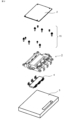
- 1 is a top view of the power conversion module according to Embodiment 1.
- FIG. 1 is a top view of the power conversion module according to Embodiment 1.
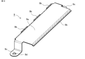
- FIG. 1 is a perspective view of a shield plate according to Embodiment 1.
- FIG. 1 is a perspective view of a DC bus bar positive electrode according to Embodiment 1.
- FIG. 1 is a perspective view of the power converter 1 according to the first embodiment
- FIG. 2 is an exploded perspective view of the power converter 1 of FIG.
- a power conversion device 1 controls on/off of a power conversion module 4 that constitutes a power conversion section housed in a housing 5, and switching elements such as IGBTs included in the power conversion module 4.
- the control board 2 includes an electronic circuit such as an IC (not shown in the figure) for the control board 2, and a bus bar assembly 3 electrically connected to the power conversion module 4.
- the power conversion module 4 is arranged in the case 5
- the busbar assembly 3 is arranged on the power conversion module 4 so as to cover the power conversion module 4, and the busbar assembly 3 is installed in the case 5. It is fastened with screws 15.
- a control board 2 is attached to the top of the bus bar assembly 3.
- the busbar assembly 3 includes a DC busbar positive electrode 6 and a DC busbar negative electrode 7 that input and output DC current, and an AC busbar 8 that is connected to a motor (not shown) and inputs and outputs the AC current converted by the power conversion module 4. It includes a shield plate 9 that shields noise generated from the power conversion module 4 due to switching of IGBTs and the like during power conversion, and a sensor core 10 that detects alternating current. For example, a capacitor (not shown) is connected to both ends of the DC bus bar positive electrode 6 and the DC bus bar negative electrode 7.
- FIG. 5 is an exploded perspective view of the bus bar assembly 3
- FIGS. 6 and 7 are top views of the power conversion module 4
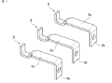
- FIGS. 8 to 11 are perspective views of the parts that make up the bus bar assembly.
- the DC busbar positive electrode 6, the DC busbar negative electrode 7, and the AC busbar 8 are arranged in the metal casing 5, if they come into direct contact with each other, they become electrical connection points and breakage occurs. Therefore, by integrally molding the DC busbar positive electrode 6, DC busbar negative electrode 7, and AC busbar 8 using a non-conductive resin 13 (hereinafter referred to as resin 13) that can provide an appropriate dielectric strength, Insulation between the DC bus bar positive electrode 6, the DC bus bar negative electrode 7, and the AC bus bar 8 and the housing 5 is maintained.
- resin 13 non-conductive resin 13
- the shield plate 9 is arranged between the DC bus bar positive electrode 6, the DC bus bar negative electrode 7, and the control board 2 (see FIGS. 5 and 2). Further, it is arranged on an extension of the flat part of the power conversion module 4 facing the switching element 16 . That is, as shown in FIG. 6, a plane part that covers at least a range 17 onto which the switching element 16 of the power conversion module 4 is projected (a plane part that covers a predetermined range on the power conversion module 4 where the switching element 16 is present) part) 9a, and is arranged on an extension of the range 17 of the power conversion module 4. As shown in FIG. 7, there are cases where a part of the shield plate is cut out and does not cover all of the individual switching elements 16, but the area is sufficient to reduce the noise of the power conversion module 4. There is no problem as long as it is covered.
- the shield plate 9 is made of aluminum material, and as shown in FIG. Suppress the deviation from 13. Holes 9d through which the screws 15 pass are formed in some of the bent portions 9c. The metal collars 11 overlap corresponding to the through holes 9d, and are connected to the housing 5 with screws 15, so that the noise generated from the power conversion module 4 is connected to the vehicle body via the shield plate 9. casing 5 to reduce noise.
- a DC busbar positive electrode 6, a DC busbar negative electrode 7 thereon, and a shield plate 9 thereon are stacked (parallel flat plates) in this order. Therefore, heat from the power conversion module 4, the DC bus bar positive electrode 6, and the DC bus bar negative electrode 7 can be efficiently radiated to the housing 5.
- the surface of the shield plate 9 may be plated for corrosion resistance. When using a pre-plated material, it is best to select a plating that can withstand the molding temperature. Further, holes may be provided in the flat portion 9a of the shield plate 9 to improve formability within a range that does not affect noise.
- the bus bar assembly 3 by integrally molding the resin 13 will be described in detail.
- the four sides of almost the entire extended portions 6a and 7a are covered with resin 13, except for the extended portions 6a and 7a.
- the four side surfaces of the extended portions 6a and 7a refer to the two faces (flat parts of the extended portions 6a and 7a) that face each other in the thickness direction of the extended portions 6a and 7a, and those two sides. These are the two surfaces (side surfaces of the extensions 6a and 7a) that connect the two surfaces in the thickness direction. Therefore, the extending portion 6a and the extending portion 7a penetrate the resin 13 in the longitudinal direction, and the resin 13 surrounds the four sides of the extending portion 6a and the extending portion 7a.
- the two DC bus bar positive electrodes 6 and the DC bus bar negative electrodes 7 are kept parallel to each other and separated from each other, and the resin 13 is interposed between them.
- the shield plate 9 also maintains a parallel and separated state, with a resin 13 interposed therebetween.
- a non-conductive molded member 14a and a non-conductive molded member 14b may be interposed.
- the DC bus bar positive electrode 6 and the DC bus bar negative electrode 7 are arranged on the lower side where the shield plate 9 is arranged, and the AC bus bar 8 and the sensor core are connected to each other except for the flat part 9a of the shield plate 9 facing the control board 2. Together with 10, it is integrally molded with non-conductive resin 13.
- the AC bus bar 8 has an AC connecting portion 8b at one end. Note that in this embodiment, there are three AC bus bars 8, but the number is not particularly limited.
- the DC busbar positive electrode 6, the DC busbar negative electrode 7, and the AC busbar 8 are preferably made of copper from the viewpoint of power efficiency.
- the linear expansion coefficient of the resin 13 close to the thermal expansion coefficient of the DC busbar positive electrode 6, the DC busbar negative electrode 7, and the AC busbar 8
- at least one of the DC busbar positive electrode 6, the DC busbar negative electrode 7, and the AC busbar 8 It is possible to eliminate resin peeling or cracking due to temperature rise.
- the bus bar assembly 3 is formed in which the shield plate 9 is integrally molded with the DC bus bar positive electrode 6, the DC bus bar negative electrode 7, the AC bus bar 8, and the sensor core 10. Therefore, screw fastening of the shield plate 9 can be eliminated. This makes it possible to reduce the number of parts. This simplifies the assembly process, improving work efficiency and yield. In addition, by being integrally molded with the bus bar, the height can be reduced, and miniaturization is also possible. Note that the shield plate 9 may be covered with the resin 13 as long as the components mounted on the control board 2 are not affected.
- the nut 12 may be integrally molded with the resin 13 and used as a terminal block. Further, the metal collar 11 may be integrally molded with the DC bus bar positive electrode 6, the DC bus bar negative electrode 7, the AC bus bar 8, the shield plate 9, and the sensor core 10. The resin 13 is tightened and fixed to the casing by screws 15 while facing or in contact with the casing 5. Such a structure makes it possible to withstand on-vehicle vibrations.
Landscapes
- Engineering & Computer Science (AREA)
- Power Engineering (AREA)
- Inverter Devices (AREA)
Abstract
Description
スイッチング素子を有し、スイッチング素子のオン、オフにより直流と交流との電力変換を行う電力変換モジュールと、電力変換モジュールの直流端子と接続され、直流電流を入出力するための正極、負極を有する直流バスバと、電力変換モジュールの交流端子と接続され、交流電流を入出力するための交流バスバと、交流電流を検出するセンサコアと、シールドプレートと、電力変換モジュールのオン、オフを制御するための電子回路を備えた制御基板と、を備え、直流バスバは、平板状の直流バスバ正極と平板状の直流バスバ負極とからなり、直流バスバ正極、直流バスバ負極、シールドプレートは非導電性の部材を介して積層され、交流バスバおよびセンサコアと共に樹脂により一体化されたバスバアセンブリが構成され、バスバアセンブリが電力変換モジュールと制御基板との間に配設されていることを特徴とする。
図1は、実施の形態1の電力変換装置1の斜視図、図2は、図1の電力変換装置1の分解斜視図である。図1、図2において、電力変換装置1は、筐体5に収容される電力変換部を構成する電力変換モジュール4と、電力変換モジュール4が有するIGBTなどのスイッチング素子のオン、オフを制御するためのICなどの電子回路(図中、省略)を備えた制御基板2と、電力変換モジュール4と電気的に接続されるバスバアセンブリ3とを備える。
従って、例示されていない無数の変形例が、本願に開示される技術の範囲内において想定する場合が含まれるものとする。
Claims (5)
- スイッチング素子を有し、前記スイッチング素子のオン、オフにより直流と交流との電力変換を行う電力変換モジュールと、前記電力変換モジュールの直流端子と接続され、直流電流を入出力するための正極、負極を有する直流バスバと、前記電力変換モジュールの交流端子と接続され、交流電流を入出力するための交流バスバと、前記交流電流を検出するセンサコアと、シールドプレートと、前記電力変換モジュールのオン、オフを制御するための電子回路を備えた制御基板と、を備え、前記直流バスバは、平板状の直流バスバ正極と平板状の直流バスバ負極とからなり、前記直流バスバ正極、前記直流バスバ負極、前記シールドプレートは非導電性の部材を介して積層され、前記交流バスバおよび前記センサコアと共に非導電性の樹脂により一体化されたバスバアセンブリが構成され、前記バスバアセンブリは前記電力変換モジュールと前記制御基板との間に配設されていることを特徴とする電力変換装置。
- 前記シールドプレートは、前記電力変換モジュールで発生するノイズを筐体に流すために、前記スイッチング素子が存在する前記電力変換モジュール上のあらかじめ定められた範囲を覆う平面部を有することを特徴とする請求項1に記載の電力変換装置。
- 前記シールドプレートは、端部に折り曲げ部を有し、前記折り曲げ部は前記非導電性の樹脂に覆われ、前記制御基板との対向面は、前記非導電性の樹脂から露出していることを特徴とする請求項2に記載の電力変換装置。
- 前記シールドプレートは、金属カラーを介して筐体と接続されていることを特徴とする請求項1から3のいずれか1項に記載の電力変換装置。
- 前記金属カラーは、前記バスバアセンブリに前記非導電性の樹脂により一体化されていることを特徴とする請求項4に記載の電力変換装置。
Priority Applications (1)
| Application Number | Priority Date | Filing Date | Title |
|---|---|---|---|
| CN202280095515.7A CN119137848A (zh) | 2022-05-10 | 2022-10-31 | 电力转换装置 |
Applications Claiming Priority (2)
| Application Number | Priority Date | Filing Date | Title |
|---|---|---|---|
| JP2022-077393 | 2022-05-10 | ||
| JP2022077393A JP7224513B1 (ja) | 2022-05-10 | 2022-05-10 | 電力変換装置 |
Publications (1)
| Publication Number | Publication Date |
|---|---|
| WO2023218681A1 true WO2023218681A1 (ja) | 2023-11-16 |
Family
ID=85226240
Family Applications (1)
| Application Number | Title | Priority Date | Filing Date |
|---|---|---|---|
| PCT/JP2022/040687 Ceased WO2023218681A1 (ja) | 2022-05-10 | 2022-10-31 | 電力変換装置 |
Country Status (3)
| Country | Link |
|---|---|
| JP (1) | JP7224513B1 (ja) |
| CN (1) | CN119137848A (ja) |
| WO (1) | WO2023218681A1 (ja) |
Citations (4)
| Publication number | Priority date | Publication date | Assignee | Title |
|---|---|---|---|---|
| JP2006031959A (ja) * | 2004-07-12 | 2006-02-02 | Nissan Motor Co Ltd | バスバー |
| JP2014168360A (ja) * | 2013-02-28 | 2014-09-11 | Mitsubishi Heavy Ind Ltd | 電力変換モジュール結線用のバスバーアッセンブリ |
| WO2016125638A1 (ja) * | 2015-02-06 | 2016-08-11 | 日立オートモティブシステムズ株式会社 | 電流センサ |
| JP2017156319A (ja) * | 2016-03-04 | 2017-09-07 | トヨタ自動車株式会社 | 電流センサユニット |
-
2022
- 2022-05-10 JP JP2022077393A patent/JP7224513B1/ja active Active
- 2022-10-31 CN CN202280095515.7A patent/CN119137848A/zh active Pending
- 2022-10-31 WO PCT/JP2022/040687 patent/WO2023218681A1/ja not_active Ceased
Patent Citations (4)
| Publication number | Priority date | Publication date | Assignee | Title |
|---|---|---|---|---|
| JP2006031959A (ja) * | 2004-07-12 | 2006-02-02 | Nissan Motor Co Ltd | バスバー |
| JP2014168360A (ja) * | 2013-02-28 | 2014-09-11 | Mitsubishi Heavy Ind Ltd | 電力変換モジュール結線用のバスバーアッセンブリ |
| WO2016125638A1 (ja) * | 2015-02-06 | 2016-08-11 | 日立オートモティブシステムズ株式会社 | 電流センサ |
| JP2017156319A (ja) * | 2016-03-04 | 2017-09-07 | トヨタ自動車株式会社 | 電流センサユニット |
Also Published As
| Publication number | Publication date |
|---|---|
| CN119137848A (zh) | 2024-12-13 |
| JP2023166700A (ja) | 2023-11-22 |
| JP7224513B1 (ja) | 2023-02-17 |
Similar Documents
| Publication | Publication Date | Title |
|---|---|---|
| US10362703B2 (en) | Electric motor inverter | |
| JP3793407B2 (ja) | 電力変換装置 | |
| US20110221268A1 (en) | Power Converter and In-Car Electrical System | |
| JP2018207718A (ja) | 電力変換装置 | |
| JP4538474B2 (ja) | インバータ装置 | |
| US10163761B2 (en) | Power semiconductor arrangement | |
| JP6326038B2 (ja) | 電気回路装置 | |
| CN109412431B (zh) | 叠层铜排及三相大功率逆变器 | |
| JP7627852B1 (ja) | 電気接続箱 | |
| JP2000092847A (ja) | コンデンサ付き半導体モジュール装置 | |
| JP4055643B2 (ja) | インバータ装置 | |
| JP3651444B2 (ja) | 電力変換装置 | |
| CN113826315A (zh) | 电力转换装置 | |
| JP6647350B2 (ja) | 電力変換装置 | |
| JP7224513B1 (ja) | 電力変換装置 | |
| WO2022264864A1 (ja) | バスバー放熱構造及びインバータ装置 | |
| JP2002291261A (ja) | 電力変換装置 | |
| CN113574787B (zh) | 功率转换装置和功率转换装置的制造方法 | |
| JP7191157B1 (ja) | スイッチング装置 | |
| WO2020152898A1 (ja) | パワー半導体装置 | |
| JPH1014254A (ja) | 電気車用制御装置 | |
| JP2009525015A (ja) | 特にモータ及び/又は発電機で運転可能な電気機械を制御するための電気的な装置 | |
| JP2007037211A (ja) | 配電部品および電気装置 | |
| JP7119430B2 (ja) | 電力変換装置 | |
| EP4498592B1 (en) | Power module and power conversion device |
Legal Events
| Date | Code | Title | Description |
|---|---|---|---|
| 121 | Ep: the epo has been informed by wipo that ep was designated in this application |
Ref document number: 22941757 Country of ref document: EP Kind code of ref document: A1 |
|
| WWE | Wipo information: entry into national phase |
Ref document number: 18855108 Country of ref document: US |
|
| WWE | Wipo information: entry into national phase |
Ref document number: 202280095515.7 Country of ref document: CN |
|
| NENP | Non-entry into the national phase |
Ref country code: DE |
|
| 122 | Ep: pct application non-entry in european phase |
Ref document number: 22941757 Country of ref document: EP Kind code of ref document: A1 |