WO2023218623A1 - 光受信器、親局装置および光通信システム - Google Patents
光受信器、親局装置および光通信システム Download PDFInfo
- Publication number
- WO2023218623A1 WO2023218623A1 PCT/JP2022/020159 JP2022020159W WO2023218623A1 WO 2023218623 A1 WO2023218623 A1 WO 2023218623A1 JP 2022020159 W JP2022020159 W JP 2022020159W WO 2023218623 A1 WO2023218623 A1 WO 2023218623A1
- Authority
- WO
- WIPO (PCT)
- Prior art keywords
- signal
- adjustment value
- circuit
- optical
- adjustment
- Prior art date
- Legal status (The legal status is an assumption and is not a legal conclusion. Google has not performed a legal analysis and makes no representation as to the accuracy of the status listed.)
- Ceased
Links
Images



Classifications
-
- H—ELECTRICITY
- H04—ELECTRIC COMMUNICATION TECHNIQUE
- H04B—TRANSMISSION
- H04B10/00—Transmission systems employing electromagnetic waves other than radio-waves, e.g. infrared, visible or ultraviolet light, or employing corpuscular radiation, e.g. quantum communication
- H04B10/60—Receivers
- H04B10/66—Non-coherent receivers, e.g. using direct detection
- H04B10/69—Electrical arrangements in the receiver
- H04B10/693—Arrangements for optimizing the preamplifier in the receiver
- H04B10/6933—Offset control of the differential preamplifier
-
- H—ELECTRICITY
- H04—ELECTRIC COMMUNICATION TECHNIQUE
- H04B—TRANSMISSION
- H04B10/00—Transmission systems employing electromagnetic waves other than radio-waves, e.g. infrared, visible or ultraviolet light, or employing corpuscular radiation, e.g. quantum communication
- H04B10/27—Arrangements for networking
-
- H—ELECTRICITY
- H04—ELECTRIC COMMUNICATION TECHNIQUE
- H04B—TRANSMISSION
- H04B10/00—Transmission systems employing electromagnetic waves other than radio-waves, e.g. infrared, visible or ultraviolet light, or employing corpuscular radiation, e.g. quantum communication
- H04B10/60—Receivers
- H04B10/66—Non-coherent receivers, e.g. using direct detection
- H04B10/69—Electrical arrangements in the receiver
-
- H—ELECTRICITY
- H04—ELECTRIC COMMUNICATION TECHNIQUE
- H04B—TRANSMISSION
- H04B10/00—Transmission systems employing electromagnetic waves other than radio-waves, e.g. infrared, visible or ultraviolet light, or employing corpuscular radiation, e.g. quantum communication
- H04B10/60—Receivers
- H04B10/66—Non-coherent receivers, e.g. using direct detection
- H04B10/69—Electrical arrangements in the receiver
- H04B10/693—Arrangements for optimizing the preamplifier in the receiver
- H04B10/6931—Automatic gain control of the preamplifier
-
- H—ELECTRICITY
- H04—ELECTRIC COMMUNICATION TECHNIQUE
- H04B—TRANSMISSION
- H04B10/00—Transmission systems employing electromagnetic waves other than radio-waves, e.g. infrared, visible or ultraviolet light, or employing corpuscular radiation, e.g. quantum communication
- H04B10/60—Receivers
- H04B10/66—Non-coherent receivers, e.g. using direct detection
- H04B10/69—Electrical arrangements in the receiver
- H04B10/695—Arrangements for optimizing the decision element in the receiver, e.g. by using automatic threshold control
Definitions
- the present disclosure relates to an optical receiver, a master station device, and an optical communication system used in an optical communication system.
- a PON system is composed of one OLT (Optical Line Terminal), which is a master station device, and ONU (Optical Network Unit), which is a plurality of subscriber side terminal devices and is also called a slave station device.
- OLT Optical Line Terminal
- ONU Optical Network Unit
- the OLT and ONU are connected via an optical star coupler, which is a passive element that does not require a power source and is an optical branching device that branches optical signals.
- a time division multiplexing method is used in upstream communication from the ONU to the OLT, in which the OLT gives permission to the ONU regarding the transmission timing and amount of data to be transmitted.
- the ONU performs uplink communication using the permitted amount of data to be transmitted at the timing permitted by the OLT.
- the strength of the upstream optical signal received by the OLT is not constant. For this reason, upstream signals of various strengths arrive at the OLT intermittently from a plurality of ONUs.
- the range of the intensity of the optical signal received by the OLT is limited to some extent because it is determined by standards, but it ranges from a weak signal of about -30 dBm to a strong signal of about -10 dBm, for example.
- the OLT must receive optical signals with intensities that differ by a factor of 100 or more.
- the OLT must amplify the signal with a high conversion gain for processing such as clock data recovery. For this reason, preamplifiers that have a high conversion gain and can convert a current signal from a light receiving element into a voltage signal are widely used.
- preamplifiers that have a high conversion gain and can convert a current signal from a light receiving element into a voltage signal are widely used.
- waveform distortion occurs in the amplifier. For this reason, a method of adjusting the conversion gain of an amplifier after receiving an optical signal is widely used.
- the preamplifier is equipped with a single-phase differential conversion circuit in order to convert the input to the subsequent amplifier into a differential signal, so if the conversion gain is adjusted, the threshold of the single-phase differential conversion circuit must also be adjusted. There is. In the method of adjusting the conversion gain and threshold after receiving an optical signal, the preamplifier cannot output a normal waveform during the convergence time from when receiving the optical signal starts until the adjustment is completed. Can not. Therefore, the shorter the convergence time, the better.
- Patent Document 1 discloses a method of switching the time constants of an automatic gain adjustment circuit for adjusting the conversion gain and an automatic threshold control circuit for adjusting the threshold according to the signal detection result. Proposed.
- the automatic gain adjustment circuit will be referred to as AGC (Automatic Gain Control)
- the automatic threshold control circuit will be referred to as ATC (Automatic Threshold Control).
- the time constants of AGC and ATC are made small during the adjustment period, and the time constants of AGC and ATC are made large after the adjustment is completed. This makes it possible to shorten the convergence time.
- the present disclosure has been made in view of the above, and it is an object of the present disclosure to obtain an optical receiver that can further shorten the convergence time, which is the time taken from the start of reception of an optical signal to the completion of adjustment of conversion gain and threshold value. With the goal.
- an optical receiver provides a master station that receives optical signals in a time division multiplexing manner from a plurality of slave station devices connected via an optical transmission line.
- An optical receiver mounted on the device which includes a photoelectric conversion element that converts an optical signal into a current signal, a preamplifier that amplifies the current signal from the photoelectric conversion element and converts it into a voltage signal, and a preamplifier that converts an optical signal into a current signal.
- the preamplifier includes a core amplifier circuit that amplifies the current signal, an automatic gain control circuit that changes the conversion gain of the core amplifier circuit by adjusting the first adjustment value, and a single amplifier that the core amplifier circuit outputs.
- the core amplifier circuit includes a single-phase differential conversion circuit that converts a phase signal into a differential signal, an automatic threshold control circuit that changes the threshold of the single-phase differential conversion circuit by adjusting a second adjustment value, and an automatic gain control circuit.
- the first adjustment value adjusted based on the output of the core amplifier circuit and the second adjustment value adjusted by the automatic threshold value control circuit based on the output of the core amplifier circuit are associated with identification information of the slave station device received from the host system. and a processing device for storing the information in the storage unit.
- the optical receiver according to the present disclosure has the effect that it is possible to further shorten the convergence time, which is the time it takes from the start of receiving an optical signal to the completion of adjustment of the conversion gain and threshold value.
- FIG. 1 A diagram showing the configuration of an optical communication system according to Embodiment 1 Diagram showing the configuration of the optical receiver shown in FIG. 1 Diagram showing observation points in the preamplifier shown in Figure 2 Diagram showing a simplified example of the time waveform at the observation point shown in Figure 3
- An explanatory diagram of the registration process of the first adjustment value and the second adjustment value by the optical receiver shown in FIG. 2 A diagram showing the configuration of an optical receiver according to Embodiment 2
- FIG. 3 A diagram showing the configuration of an optical receiver according to Embodiment 3
- FIG. 1 is a diagram showing the configuration of an optical communication system 5 according to the first embodiment.
- the optical communication system 5 is a PON system including an OLT 1 and a plurality of ONUs 2-1 to 2-3.
- the OLT 1 is also called a master station device, and is connected to a plurality of ONUs 2-1 to 2-3 using an optical splitter 3 that branches an optical transmission path and an optical fiber 4. Note that if there is no need to distinguish each of the plurality of ONUs 2-1 to 2-3, they are simply referred to as ONU 2.
- the ONU 2 is also called a slave station device.
- one OLT 1 is connected to three ONUs 2 here, the number of ONUs 2 connected to one OLT 1 is not limited to three. The number of ONUs 2 connected to one OLT 1 may be two or four or more.
- a time division multiplexing method is used in upstream communication from the ONU 2 to the OLT 1, in which the OLT 1 gives permission to each of the plurality of ONUs 2 regarding the transmission timing and amount of data to be transmitted. Therefore, the OLT 1 knows in advance which ONU 2 among the ONUs 2-1 to 2-3 is the transmission source of the received optical signal.
- the OLT 1 has an optical receiver 10 that receives optical signals.
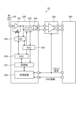
- FIG. 2 is a diagram showing the configuration of the optical receiver 10 shown in FIG. 1.
- the optical receiver 10 includes an APD (Avalanche Photo Diode) 100 that is a photoelectric conversion element that converts an optical signal into a current signal, a preamplifier 200 that amplifies the current signal from the APD 100, and converts it into a voltage signal.
- a limiting amplifier 300 that further amplifies the voltage signal from the amplifier 200 and limits the amplitude of the voltage signal to a predetermined range, and a clock data recovery that extracts and reproduces a clock and data from the signal from the limiting amplifier 300.
- a host system 400 having functions.
- the host system 400 further supplies a reset signal to each of the preamplifier 200 and the limiting amplifier 300, supplies ONU information to the preamplifier 200, and determines the signal arrival time from each of the plurality of ONUs 2 and the ONU 2. manage identification information.
- the ONU information includes, for example, identification information of the ONU 2 that is the transmission source of the optical signal to be received next.
- the APD 100 converts the received optical signal into a current signal and outputs it to the preamplifier 200.
- the preamplifier 200 amplifies the current signal output by the APD 100, converts it into a voltage signal, and outputs the voltage signal to the limiting amplifier 300.
- the limiting amplifier 300 further amplifies the voltage signal output by the preamplifier 200, limits the amplitude of the voltage signal to a predetermined range, and outputs the voltage signal to the host system 400.
- the host system 400 extracts and reproduces the clock and data from the signal output by the limiting amplifier 300.
- the preamplifier 200 controls the operation of the preamplifier 200 based on a reset signal output by the host system 400 and ONU information including identification information of the ONU 2.
- the preamplifier 200 includes a core amplifier circuit 201, an automatic gain control circuit AGC 202, an automatic threshold control circuit ATC 203, a single-phase differential conversion circuit 204, an ADC (Analog Digital Converter) 205, and a DAC (Digital Converter) 205. Converter) 206, a storage unit 207, and a processing device 208.
- the core amplification circuit 201 amplifies the current signal from the APD 100.
- the conversion gain of the core amplifier circuit 201 is adjusted by the AGC 202.
- the output of the core amplifier circuit 201 is connected to each of the AGC 202, ATC 203, and single-phase differential conversion circuit 204.
- the AGC 202 has a function of adjusting the conversion gain of the core amplifier circuit 201.
- the AGC 202 can change the conversion gain of the core amplifier circuit 201 by adjusting the value of the first adjustment value output to the core amplifier circuit 201.
- the AGC 202 has a function of adjusting the first adjustment value and adjusting the conversion gain based on the output of the core amplification circuit 201 so that the output of the core amplification circuit 201 becomes a predetermined level.
- the AGC 202 also has a function of changing the conversion gain by outputting the first adjustment value received from the DAC 206 to the core amplifier circuit 201 when the AGC 202 receives the first adjustment value from the DAC 206 .
- the first adjustment value is a voltage value, and is supplied to a feedback resistance section (not shown) of the core amplifier circuit 201.
- the feedback resistor section is generally a parallel circuit of a resistor and a MOSFET (Metal-Oxide-Semiconductor Field-Effect Transistor).
- the first adjustment value acts as a gate voltage of the MOSFET that constitutes the feedback resistance section of the core amplifier circuit 201.
- the gate voltage of the MOSFET changes, and the resistance value of the feedback resistance section changes, resulting in a change in the signal amplification gain of the core amplifier circuit 201.
- the higher the resistance value of the feedback resistor section the higher the gain, and the lower the resistance value, the lower the gain.
- the ATC 203 has a function of adjusting the threshold of the single-phase differential conversion circuit 204.
- the ATC 203 can change the threshold value input to the single-phase differential conversion circuit 204 by adjusting the second adjustment value output to the single-phase differential conversion circuit 204.
- the ATC 203 has a function of adjusting the second adjustment value based on the output of the core amplifier circuit 201 and adjusting the threshold value of the single-phase differential conversion circuit 204.
- the ATC 203 also has a function of adjusting the threshold value by outputting the second adjustment value received from the DAC 206 to the single-phase differential conversion circuit 204 when the ATC 203 receives the second adjustment value from the DAC 206 .
- the second adjustment value is a voltage value, and is the input voltage of one of the two inputs of the differential amplifier circuit that constitutes the single-phase differential conversion circuit 204.
- the single-phase differential conversion circuit 204 receives the output of the core amplifier circuit 201 and the threshold value that is the output of the ATC 203 as input, and converts the single-phase signal into a differential signal.
- the positive phase input of the single-phase differential conversion circuit 204 can be used as the output of the core amplifier circuit 201
- the negative phase input of the single-phase differential conversion circuit 204 can be used as the threshold value that is the output of the ATC 203.
- the differential amplifier circuit that constitutes the single-phase differential conversion circuit 204 is a general MOSFET-based CML (Current Model Logic) circuit, a bipolar transistor-based ECL (Emitter Coupled Logic), or the like.
- the second adjustment value acts as a gate voltage of the MOSFET that configures the CML circuit.
- the second adjustment value acts as a base voltage of the bipolar transistor that constitutes the ECL.
- the center of the positive phase input signal of the single-phase differential conversion circuit 204 is set to DC1
- the center of the negative phase input signal is set to DC2.
- the value of the DC offset "DC1-DC2" is ideally 0 mV in order to obtain a high amplification factor and an output differential signal without distortion. Examples of undistorted signals include a sine wave with a duty ratio of 50%.
- the amplification factor of the single-phase differential conversion circuit 204 decreases, causing distortion in the signal waveform of the output differential signal.
- the amplitude of the output voltage of the core amplifier circuit 201 is constant, the more the value of "DC1-DC2” deviates from 0 mV, the more the output voltage amplitude of the single-phase differential conversion circuit 204 decreases, and the duty ratio also decreases from 50%. It shifts. Therefore, in the optical receiver 10, in order to bring the value of "DC1-DC2" closer to 0 mV, the value of DC2 is controlled to be closer to DC1.
- the value of DC2 is the output of the ATC 203, that is, the second adjustment value, and becomes the threshold of the single-phase differential conversion circuit 204. Therefore, the receiver 10 controls the second adjustment value so that it approaches the value of DC1, that is, the center of the output signal of the core amplification circuit 201.
- the differential signal output from the single-phase differential conversion circuit 204 is input to the limiting amplifier 300.
- ADC 205 converts analog values into digital values.
- the ADC 205 can convert the first adjustment value and the second adjustment value, which are analog values output by the AGC 202 and ATC 203, into digital values, and can output the converted digital values to the storage unit 207.
- the DAC 206 converts digital values into analog values.
- the DAC 206 can convert the first adjustment value stored in the storage unit 207 from a digital value to an analog value, and output the first adjustment value, which is the converted analog value, to the AGC 202 . Further, the DAC 206 can convert the second adjustment value stored in the storage unit 207 from a digital value to an analog value, and output the second adjustment value, which is the converted analog value, to the ATC 203.
- the storage unit 207 has a function of holding the first adjustment value and the second adjustment value, which are digital values output by the ADC 205.
- the storage unit 207 can output the held first adjustment value and second adjustment value to the DAC 206 in response to an instruction from the processing device 208.
- the processing device 208 is a simple circuit that controls the operation of the preamplifier 200.
- the processing device 208 can receive a reset signal and ONU information from the host system 400 and control the operation of the preamplifier 200 based on the information received from the host system 400. Details of the control performed by the processing device 208 will be described later.
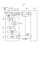
- FIG. 3 is a diagram showing observation points in the preamplifier 200 shown in FIG. 2.
- FIG. 4 is a diagram schematically showing an example of a time waveform at the observation point shown in FIG. 3.
- Observation point A is an input point to APD 100, and an optical signal input to APD 100 is observed.
- Observation point B is the output point of the core amplification circuit 201, and the signal after being amplified by the core amplification circuit 201 is observed.
- Observation point C is the output point from AGC 202 to core amplification circuit 201, and the first adjustment value is observed.
- Observation point D is the output point of ATC 203, and the second adjustment value is observed.
- Observation point E is an input point from host system 400 to processing device 208, and a reset signal is observed.
- the optical signal from ONU 2 is received at time T.
- the reset signal is supplied so that it can be observed at the observation point E in accordance with the arrival of the optical signal at time T.
- the core amplifier circuit 201 After receiving the optical signal, the core amplifier circuit 201 performs inversion amplification, so as observed at observation point B, the output of the core amplifier circuit 201 significantly lowers the DC (Direct Current) level.
- the broken line in the graph at observation point B represents the output level of the core amplifier circuit 201 when an appropriate conversion gain is achieved.
- observation point C when the AGC 202 and ATC 203 each adjust the conversion gain and threshold by adjusting the first adjustment value and the second adjustment value based on the output of the core amplification circuit 201 as before.
- the time waveform at observation point D is indicated by a dashed line.
- the AGC 202 determines whether the output of the core amplification circuit 201 is higher or lower than the appropriate level, and as shown in FIG. If it is determined that the output of the circuit 201 is lower than the appropriate level, the first adjustment value is adjusted to lower the conversion gain. Note that here it is assumed that the larger the value of the first adjustment value observed at observation point C, the lower the conversion gain, but conversely, the smaller the value of the first adjustment value is, the lower the conversion gain is. good. Here, the time required for adjusting the AGC 202 is assumed to be t1. t1 is about several tens of ns in the case of a high-speed one.
- observation point D exhibits behavior similar to observation point B. However, this may not apply depending on the circuit design.
- the second adjustment value observed at observation point D is preferably a value that matches the DC level of the output of the core amplification circuit 201 observed at observation point B, so it can be observed using a low-pass filter or the like.
- the second adjustment value may be generated by dropping high frequency components from the waveform at point B. In this case, the waveform at observation point D fluctuates gradually over time.
- the optical receiver 10 holds a first adjustment value and a second adjustment value registered in advance for each ONU 2 in the storage unit 207 .
- the timing at which the optical signal arrives from each ONU 2 is known. Therefore, the optical receiver 10 changes the conversion gain and threshold using the first adjustment value and the second adjustment value registered in advance in accordance with the arrival of the optical signal, thereby reducing the time required for adjustment. It is possible to shorten.
- the time waveforms at observation point C and observation point D in FIG. 4 are represented by broken lines. The times t1 and t2 required for adjustment can theoretically be set to zero.
- the host system 400 of the optical receiver 10 outputs a reset signal to the preamplifier 200 in accordance with the known signal reception timing, and the processing device 208 of the preamplifier 200 outputs the reset signal to the storage unit 207 in accordance with the reset signal.
- the first adjustment value and the second adjustment value stored in are supplied to each of AGC 202 and ATC 203.
- AGC 202 uses the supplied first adjustment value to change the conversion gain, and
- ATC 203 uses the supplied second adjustment value to change the threshold value.
- the first adjustment value and the second adjustment value to be used must be adjusted in advance. You need to register. Registration of the first adjustment value and the second adjustment value will be described below.
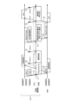
- FIG. 5 is an explanatory diagram of the registration process of the first adjustment value and the second adjustment value by the optical receiver 10 shown in FIG. 2.
- FIG. 5 shows the received signal of OLT1, the transmitted signal of OLT1, the internal signal of OLT1, the output of AGC 202 in preamplifier 200 of OLT1, the state of preamplifier 200, the received signal of ONU2, and the transmitted signal of ONU2. has been done.
- the internal signal of the OLT 1 refers to a signal exchanged between the host system 400 and the preamplifier 200 within the OLT 1, for example.
- the ONU 2 is one of the ONUs 2-1 to 2-3 shown in FIG.
- FIG. 5 starts from the time when the ONU 2 is first connected to the network.
- the OLT 1 transmits a Gate signal to check whether the newly connected ONU 2 exists in the network (step S1).
- the Gate signal is supplied to the preamplifier 200 as an internal signal (step S2).
- the electrical path for supplying the Gate signal to the preamplifier 200 may be a signal line for supplying the reset signal shown in FIG. 2, or a signal line for supplying the ONU information shown in FIG. Alternatively, a new signal line different from these signal lines may be provided.
- the preamplifier 200 When the preamplifier 200 receives the Gate signal, it shifts to a "Reg.stand-by" state in which it performs registration processing of the first adjustment value and the second adjustment value. Note that in the following description, the first adjustment value and the second adjustment value may be simply referred to as adjustment values.
- the ONU 2 Upon receiving the Gate signal, the ONU 2 transmits a registration request including information necessary for registering itself to the network to the OLT 1 (step S3).
- the OLT 1 When the OLT 1 receives the registration request from the ONU 2, since the adjustment value suitable for this ONU 2 is unknown at this stage, the adjustment process of the adjustment value based on the output of the core amplifier circuit 201 is performed as before. .
- the OLT 1 supplies a reset signal indicating that the signal from the ONU 2 has been received to the preamplifier 200 as an internal signal (step S4).
- Preamplifier 200 converts the adjustment value at the stage of receiving this reset signal into a digital signal and registers it in storage section 207 . At this stage, the registered adjustment value is not associated with the identification information of the ONU 2. Further, when a reset signal is supplied as an internal signal (step S5), the preamplifier 200 releases the adjustment value registration state.
- the OLT 1 After receiving the registration request, the OLT 1 determines the transmission timing and amount of data to be transmitted by the ONU 2, and transmits a "Register+gate" signal that includes the allocation information and is a registration confirmation signal to the ONU 2 (step S6). At this time, the OLT 1 supplies a data string including the identification information of the ONU 2 as an internal signal to the preamplifier 200 (step S7). When the preamplifier 200 receives this identification information, it registers the adjustment value already stored in the storage unit 207 in association with the received identification information. For example, the preamplifier 200 can associate the adjustment value with the identification information by associating the identification information of the ONU 2 with the register address.
- the ONU 2 Upon receiving the "Register+gate" signal, the ONU 2 transmits an Ack signal to confirm that it has been received (step S8). At this stage, since the arrival timing of the signal from the ONU 2 is known, the OLT 1 transmits the reset signal and the identification information that identifies the ONU 2 that is the source of the received signal to the internal signal in accordance with the reception timing of the Ack signal. (Step S9).
- the preamplifier 200 retrieves the adjustment values stored in the storage unit 207 in association with the supplied identification information in accordance with the reset signal, and supplies them to each of the AGC 202 and ATC 203. By doing this, you can instantly complete the adjustment of the adjustment value. By adjusting the adjustment value, the conversion gain and the threshold value are adjusted.
- the OLT 1 supplies the reset signal as an internal signal to the preamplifier 200 (step S10).
- the preamplifier 200 releases the adjustment value calling state at a timing matching this reset signal.
- the optical receiver 10 is connected to a plurality of ONUs 2, which are slave station devices, via an optical transmission path, and receives optical signals from the plurality of ONUs 2 in a time division multiplexing manner.
- An optical receiver 10 mounted on the OLT 1, which is a master station device, includes an APD 100, which is a photoelectric conversion element that converts an optical signal into a current signal, and a front end that amplifies the current signal from the APD 100 and converts it into a voltage signal.
- An amplifier 200 a limiting amplifier 300 that further amplifies the voltage signal from the preamplifier 200 and limits the amplitude of the voltage signal to a predetermined range, and a reset signal that is synchronized with the timing of receiving the optical signal.
- a host system 400 that outputs to the preamplifier 200, the preamplifier 200 includes a core amplifier circuit 201, and an automatic gain control circuit that changes the conversion gain of the core amplifier circuit by adjusting the first adjustment value.
- AGC 202 which is , a single-phase differential conversion circuit 204 that converts the single-phase signal outputted by the core amplifier circuit 201 into a differential signal, and a threshold value of the single-phase differential conversion circuit 204 is changed by adjusting the second adjustment value.
- ATC 203 which is an automatic threshold control circuit, adjusts a first adjustment value adjusted by AGC 202 based on the output of core amplifier circuit 201, and a second adjustment value adjusted by ATC 203 based on the output of core amplifier circuit 201.
- a processing device 208 that causes the storage unit 207 to store the information in association with the identification information of the ONU 2 received from the host system 400.
- the processing in which the processing device 208 associates and stores the identification information, the first adjustment value, and the second adjustment value is performed as part of the initial registration processing, for example, when the ONU 2 is connected to the network for the first time. .
- the AGC 202 changes the conversion gain of the core amplifier circuit 201 using the first adjustment value stored in the storage unit 207 at a timing that matches the reset signal, and the ATC 203 changes the conversion gain of the core amplifier circuit 201 at a timing that matches the reset signal.
- the second adjustment value stored in 207 is used to change the threshold value. In this way, adjustment of the conversion gain and threshold value can be completed at a timing that matches the reset signal supplied in accordance with the known reception timing, so that the preamplifier 200 can output a normal waveform from the beginning. It becomes possible.
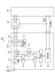
- FIG. 6 is a diagram showing the configuration of an optical receiver 10A according to the second embodiment.
- the optical receiver 10A is provided in the OLT1.
- the optical receiver 10A includes an APD 100, a preamplifier 200A, a limiting amplifier 300, and a host system 400, and includes the preamplifier 200A instead of the preamplifier 200 of the optical receiver 10.
- APD 100 an APD 100
- preamplifier 200A a preamplifier 200A
- a limiting amplifier 300 a limiting amplifier 300
- a host system 400 includes the preamplifier 200A instead of the preamplifier 200 of the optical receiver 10.
- parts that are different from the optical receiver 10 according to Embodiment 1 will be mainly described, and detailed descriptions of common parts will be omitted.
- the preamplifier 200A includes an adjustment core amplifier circuit 209 that amplifies the current signal from the APD 100, and adjusts a third adjustment value based on the output of the adjustment core amplifier circuit 209.
- AGC 210 which is an automatic gain control circuit for adjustment that changes the conversion gain of the core amplifier circuit 209 for adjustment by changing the conversion gain of the core amplifier circuit 209 for adjustment; and automatic threshold value control for adjustment that adjusts the fourth adjustment value based on the output of the core amplifier circuit 209 for adjustment.
- the processing device 208 converts the third adjustment value after the adjustment by the AGC 210 and the fourth adjustment value after the adjustment by the ATC 211 into digital values using the ADC 205, and stores the third adjustment value after the conversion using the third adjustment value.
- the first adjustment value stored in the storage unit 207 can be updated, and the second adjustment value stored in the storage unit 207 can be updated using the fourth adjustment value after adjustment by the ATC 211.
- the processing device 208 updates the first adjustment value and the second adjustment value that were used when adjusting the third adjustment value and the fourth adjustment value.
- the optical receiver 10A can update the first adjustment value and the second adjustment value once registered in the storage unit 207. Therefore, even if the appropriate adjustment value changes due to environmental changes, deterioration over time, etc., it is possible to follow such changes.
- FIG. 7 is a diagram showing the configuration of an optical receiver 10B according to the third embodiment.
- the optical receiver 10B is included in the OLT1.
- the optical receiver 10B includes an APD 100, a preamplifier 200B, a limiting amplifier 300, and a host system 400, and includes a preamplifier 200B instead of the preamplifier 200 of the optical receiver 10.
- APD 100 an APD 100
- preamplifier 200B a preamplifier 200B
- a limiting amplifier 300 a limiting amplifier 300
- a host system 400 includes a preamplifier 200B instead of the preamplifier 200 of the optical receiver 10.
- parts that are different from the optical receiver 10 according to Embodiment 1 will be mainly described, and detailed descriptions of common parts will be omitted.
- the preamplifier 200B includes a signal detection circuit 212 that detects a signal included in the output of the core amplifier circuit 201, and a single-phase differential differential amplifier based on the signal detection result of the signal detection circuit 212. It has a selector 213 that switches the connection to the input terminal of the conversion circuit 204. The selector 213 can switch between a first state in which the output of the ATC 203 is connected to the differential input of the single-phase differential conversion circuit 204 and a second state in which the output of the ATC 203 is connected to the single-phase input of the single-phase differential conversion circuit 204. be.
- the output of the ATC 203 is connected to one input of the single-phase input of the single-phase differential conversion circuit 204, and the output of the core amplifier circuit 201 is connected to the other input.
- the selector 213 is in the first state after the adjustment of the conversion gain of the core amplifier circuit 201 and the threshold of the single-phase differential conversion circuit 204 is completed until the signal detection circuit 212 detects a signal. After 212 detects a signal, it enters the second state. Thereby, it is possible to suppress the occurrence of a DC offset between the differential outputs of the preamplifier 200B in a no-signal period after the reset signal is input.
- an avalanche photodiode is used as an example of a photoelectric conversion element, but the photoelectric conversion element may be a photoelectric conversion element other than an avalanche photodiode.
- the photoelectric conversion element may be a PIN junction type photodiode.
- the positive phase input of the single-phase differential conversion circuit 204 is used as the output of the core amplifier circuit 201, and the negative phase input of the single-phase differential conversion circuit 204 is used as the threshold value, which is the output of the ATC 203.
- the positive phase input of the phase-to-differential conversion circuit 204 may be used as the threshold value, which is the output of the ATC 203, and the negative phase input of the single-phase differential conversion circuit 204 may be used as the output of the core amplifier circuit 201.
Landscapes
- Engineering & Computer Science (AREA)
- Physics & Mathematics (AREA)
- Electromagnetism (AREA)
- Computer Networks & Wireless Communication (AREA)
- Signal Processing (AREA)
- Computing Systems (AREA)
- Optical Communication System (AREA)
Abstract
Description
図1は、実施の形態1にかかる光通信システム5の構成を示す図である。光通信システム5は、OLT1と、複数のONU2-1~2-3とを有するPONシステムである。OLT1は、親局装置とも呼ばれ、光伝送路を分岐させる光分岐器3と、光ファイバ4とを用いて、複数のONU2-1~2-3に接続されている。なお、複数のONU2-1~2-3のそれぞれを区別する必要がない場合、単にONU2と称する。ONU2は、子局装置とも呼ばれる。ここでは1台のOLT1が3台のONU2に接続されているが、1台のOLT1に接続されるONU2の台数は3台に限らない。1台のOLT1に接続されるONU2の台数は、2台であってもよいし、4台以上であってもよい。
図6は、実施の形態2にかかる光受信器10Aの構成を示す図である。光受信器10Aは、OLT1に備わる。光受信器10Aは、APD100と、前置増幅器200Aと、リミッティングアンプ300と、上位システム400とを有し、光受信器10の前置増幅器200の代わりに、前置増幅器200Aを有する。以下、実施の形態1にかかる光受信器10と異なる部分について主に説明し、共通する部分については詳細な説明を省略する。
図7は、実施の形態3にかかる光受信器10Bの構成を示す図である。光受信器10Bは、OLT1に備わる。光受信器10Bは、APD100と、前置増幅器200Bと、リミッティングアンプ300と、上位システム400とを有し、光受信器10の前置増幅器200の代わりに、前置増幅器200Bを有する。以下、実施の形態1にかかる光受信器10と異なる部分について主に説明し、共通する部分については詳細な説明を省略する。
Claims (8)
- 光伝送路を介して接続される複数の子局装置から時分割多重方式で光信号を受信する親局装置に実装される光受信器であって、
前記光信号を電流信号に変換する光電変換素子と、
前記光電変換素子からの電流信号を増幅すると共に電圧信号に変換する前置増幅器と、
前記前置増幅器からの前記電圧信号をさらに増幅するとともに、前記電圧信号の振幅を予め定められた範囲に制限するリミッティングアンプと、
前記光信号を受信するタイミングに合わせて、リセット信号を前記前置増幅器に出力する上位システムと、
を備え、
前記前置増幅器は、
前記電流信号を増幅するコア増幅回路と、
第1の調整値を調整することによって前記コア増幅回路の変換利得を変化させる自動利得制御回路と、
前記コア増幅回路が出力する単相信号を差動信号に変換する単相差動変換回路と、
第2の調整値を調整することによって前記単相差動変換回路の閾値を変化させる自動閾値制御回路と、
前記自動利得制御回路が前記コア増幅回路の出力に基づいて調整した前記第1の調整値と、前記自動閾値制御回路が前記コア増幅回路の出力に基づいて調整した前記第2の調整値とを、前記上位システムから受け取る前記子局装置の識別情報と対応づけて記憶部に記憶させる処理装置と、
を有することを特徴とする光受信器。 - 前記自動利得制御回路は、前記リセット信号に合わせたタイミングで、前記記憶部に記憶された前記第1の調整値を用いて前記変換利得を変化させ、
前記自動閾値制御回路は、前記リセット信号に合わせたタイミングで、前記記憶部に記憶された前記第2の調整値を用いて前記閾値を変化させることを特徴とする請求項1に記載の光受信器。 - 前記処理装置は、前記リセット信号に合わせたタイミングで、受信する光信号の送信元である前記子局装置に対応付けて前記記憶部に記憶された前記第1の調整値および前記第2の調整値を前記自動利得制御回路および前記自動閾値制御回路のそれぞれに供給することを特徴とする請求項2に記載の光受信器。
- 前記前置増幅器は、
前記光電変換素子からの前記電流信号を増幅する調整用コア増幅回路と、
前記調整用コア増幅回路の出力に基づいて第3の調整値を調整することによって前記調整用コア増幅回路の変換利得を変化させる調整用自動利得制御回路と、
前記調整用コア増幅回路の出力に基づいて第4の調整値を調整する調整用自動閾値制御回路と、
をさらに有し、
前記第3の調整値を用いて前記記憶部に記憶された前記第1の調整値を更新し、
前記第4の調整値を用いて前記記憶部に記憶された前記第2の調整値を更新することを特徴とする請求項1から3のいずれか1項に記載の光受信器。 - 前記前置増幅器は、
前記コア増幅回路の出力に含まれる信号を検出する信号検出回路と、
前記信号検出回路の信号検出結果に基づいて、前記自動閾値制御回路の出力を、前記単相差動変換回路の差動入力に接続する第1の状態と、前記単相差動変換回路の単相入力に接続する第2の状態とを切り替え可能なセレクタと、
を有し、
前記セレクタは、前記リセット信号に応じて前記自動閾値制御回路が前記第2の調整値を用いて閾値を変化させてから前記信号検出回路が信号を検出するまでの間は前記第1の状態とし、前記信号検出回路が信号を検出した後は前記第2の状態とすることを特徴とする請求項1に記載の光受信器。 - 前記光電変換素子は、アバランシェフォトダイオードであることを特徴とする請求項1に記載の光受信器。
- 請求項1から6のいずれか1項に記載の光受信器を備えることを特徴とする親局装置。
- 請求項1から6のいずれか1項に記載の光受信器を有する親局装置と、
前記親局装置と光伝送路を介して接続される複数の子局装置と、
を備えることを特徴とする光通信システム。
Priority Applications (4)
| Application Number | Priority Date | Filing Date | Title |
|---|---|---|---|
| PCT/JP2022/020159 WO2023218623A1 (ja) | 2022-05-13 | 2022-05-13 | 光受信器、親局装置および光通信システム |
| CN202280095729.4A CN119137884A (zh) | 2022-05-13 | 2022-05-13 | 光接收器、主站装置以及光通信系统 |
| JP2024506553A JP7573783B2 (ja) | 2022-05-13 | 2022-05-13 | 光受信器、親局装置および光通信システム |
| US18/894,096 US20250015898A1 (en) | 2022-05-13 | 2024-09-24 | Optical receiver, master station device, optical communication system |
Applications Claiming Priority (1)
| Application Number | Priority Date | Filing Date | Title |
|---|---|---|---|
| PCT/JP2022/020159 WO2023218623A1 (ja) | 2022-05-13 | 2022-05-13 | 光受信器、親局装置および光通信システム |
Related Child Applications (1)
| Application Number | Title | Priority Date | Filing Date |
|---|---|---|---|
| US18/894,096 Continuation US20250015898A1 (en) | 2022-05-13 | 2024-09-24 | Optical receiver, master station device, optical communication system |
Publications (1)
| Publication Number | Publication Date |
|---|---|
| WO2023218623A1 true WO2023218623A1 (ja) | 2023-11-16 |
Family
ID=88730163
Family Applications (1)
| Application Number | Title | Priority Date | Filing Date |
|---|---|---|---|
| PCT/JP2022/020159 Ceased WO2023218623A1 (ja) | 2022-05-13 | 2022-05-13 | 光受信器、親局装置および光通信システム |
Country Status (4)
| Country | Link |
|---|---|
| US (1) | US20250015898A1 (ja) |
| JP (1) | JP7573783B2 (ja) |
| CN (1) | CN119137884A (ja) |
| WO (1) | WO2023218623A1 (ja) |
Citations (6)
| Publication number | Priority date | Publication date | Assignee | Title |
|---|---|---|---|---|
| JPH11122188A (ja) * | 1997-10-20 | 1999-04-30 | Fujitsu Ltd | 光信号受信装置および方法 |
| JP2001024598A (ja) * | 1999-07-09 | 2001-01-26 | Nec Corp | 光受信回路 |
| JP2003318680A (ja) * | 2002-04-15 | 2003-11-07 | Samsung Electronics Co Ltd | 差動出力型バーストモード光受信機 |
| JP2008193271A (ja) * | 2007-02-02 | 2008-08-21 | Hitachi Communication Technologies Ltd | 受動光網システムおよびその運用方法 |
| JP5811955B2 (ja) * | 2012-06-05 | 2015-11-11 | 住友電気工業株式会社 | バースト信号の受信装置及び方法、ponの局側装置、ponシステム |
| WO2016035374A1 (ja) * | 2014-09-03 | 2016-03-10 | 三菱電機株式会社 | 光受信器、光終端装置および光通信システム |
-
2022
- 2022-05-13 WO PCT/JP2022/020159 patent/WO2023218623A1/ja not_active Ceased
- 2022-05-13 CN CN202280095729.4A patent/CN119137884A/zh active Pending
- 2022-05-13 JP JP2024506553A patent/JP7573783B2/ja active Active
-
2024
- 2024-09-24 US US18/894,096 patent/US20250015898A1/en active Pending
Patent Citations (6)
| Publication number | Priority date | Publication date | Assignee | Title |
|---|---|---|---|---|
| JPH11122188A (ja) * | 1997-10-20 | 1999-04-30 | Fujitsu Ltd | 光信号受信装置および方法 |
| JP2001024598A (ja) * | 1999-07-09 | 2001-01-26 | Nec Corp | 光受信回路 |
| JP2003318680A (ja) * | 2002-04-15 | 2003-11-07 | Samsung Electronics Co Ltd | 差動出力型バーストモード光受信機 |
| JP2008193271A (ja) * | 2007-02-02 | 2008-08-21 | Hitachi Communication Technologies Ltd | 受動光網システムおよびその運用方法 |
| JP5811955B2 (ja) * | 2012-06-05 | 2015-11-11 | 住友電気工業株式会社 | バースト信号の受信装置及び方法、ponの局側装置、ponシステム |
| WO2016035374A1 (ja) * | 2014-09-03 | 2016-03-10 | 三菱電機株式会社 | 光受信器、光終端装置および光通信システム |
Non-Patent Citations (1)
| Title |
|---|
| TAKANORI KAWANAKA; SATOSHI YOSHIMA; MASAKI NODA: "A dual‐rate burst‐mode receiver with rapid response and high CID tolerance for XGS PON", ELECTRONICS LETTERS, THE INSTITUTION OF ENGINEERING AND TECHNOLOGY, GB, vol. 57, no. 19, 2 June 2021 (2021-06-02), GB , pages 738 - 740, XP006113134, ISSN: 0013-5194, DOI: 10.1049/ell2.12237 * |
Also Published As
| Publication number | Publication date |
|---|---|
| JPWO2023218623A1 (ja) | 2023-11-16 |
| CN119137884A (zh) | 2024-12-13 |
| US20250015898A1 (en) | 2025-01-09 |
| JP7573783B2 (ja) | 2024-10-25 |
Similar Documents
| Publication | Publication Date | Title |
|---|---|---|
| US10003410B2 (en) | Optical receiver, optical termination device, and optical communication system | |
| EP2538583B1 (en) | Optical signal turn-off detection circuit and optical receiver | |
| US9496826B2 (en) | Transimpedance amplifier | |
| US20100272448A1 (en) | Optical burst signal receiving device | |
| US20110129235A1 (en) | Burst-mode optical signal receiver | |
| US8165478B2 (en) | Optical receiver | |
| KR101544077B1 (ko) | 친국측 장치 | |
| US7266312B2 (en) | Burst mode optical receiver | |
| JP2010166216A (ja) | 前置増幅器 | |
| US8433206B2 (en) | Burst-mode optical receiver and timing control method | |
| US8390383B2 (en) | Amplifier for receiving intermittent optical signal | |
| US9094134B2 (en) | Optical receiver | |
| JP6661057B1 (ja) | リミッティング増幅回路 | |
| KR100703428B1 (ko) | 버스트모드 광 수신기 및 그의 신호 크기 검출 장치 | |
| JP3606143B2 (ja) | オフセット制御回路及びそれを用いた光受信器並びに光通信システム | |
| WO2023218623A1 (ja) | 光受信器、親局装置および光通信システム | |
| US20210099235A1 (en) | Optical receiver, optical terminal, and optical communication system | |
| JP6027513B2 (ja) | 通信システム、中継装置、通信方法及び中継方法 | |
| JP2001211040A (ja) | デジタル信号増幅回路及び光受信回路 | |
| JP4691128B2 (ja) | 増幅回路 | |
| JP4590708B2 (ja) | 光受信回路 | |
| JP2009246535A (ja) | 増幅回路 | |
| US7710196B2 (en) | AC differential connection assembly between a trans-impedance amplifier and a post amplifier for burst mode receiving | |
| JP2009033627A (ja) | 光バースト信号受信装置及び光バースト信号受信装置の信号処理方法 | |
| KR20080053170A (ko) | 온칩 리셋 신호를 생성하는 버스트 모드 수신기 및 버스트모드 수신 방법 |
Legal Events
| Date | Code | Title | Description |
|---|---|---|---|
| 121 | Ep: the epo has been informed by wipo that ep was designated in this application |
Ref document number: 22941702 Country of ref document: EP Kind code of ref document: A1 |
|
| ENP | Entry into the national phase |
Ref document number: 2024506553 Country of ref document: JP Kind code of ref document: A |
|
| WWE | Wipo information: entry into national phase |
Ref document number: 202280095729.4 Country of ref document: CN |
|
| NENP | Non-entry into the national phase |
Ref country code: DE |
|
| 122 | Ep: pct application non-entry in european phase |
Ref document number: 22941702 Country of ref document: EP Kind code of ref document: A1 |